SERVICE MANUAL FACSIMILE MODEL FO-4500
SERVICE MANUAL FACSIMILE MODEL FO-4500
SERVICE MANUAL FACSIMILE MODEL FO-4500

Create successful ePaper yourself
Turn your PDF publications into a flip-book with our unique Google optimized e-Paper software.
CAUTION<br />
<strong>SERVICE</strong> <strong>MANUAL</strong><br />
SHARP CORPORATION<br />
No. 00Z<strong>FO</strong><strong>4500</strong>HSME<br />
<strong>FACSIMILE</strong><br />
<strong>MODEL</strong> <strong>FO</strong>-<strong>4500</strong><br />
This laser printer is a class 1 laser product that complies with 21CFR 1040.10 and 1040.11 of the CDRH standard. This means<br />
that this machine does not produce a hazardous laser radiation. The use of controls, adjustments or performance of procedures<br />
other than those specified herein may result in hazardous radiation exposure.<br />
This laser radiation is not a danger to the skin, but when an exact focusing of the laser beam is achieved on the eyes retina, there is<br />
danger of spot damage to the retina.<br />
The following cautions must be observed to avoid exposure of the laser beam to your eyes at the time of servicing.<br />
1) When a problem in the laser optical unit has occurred, the whole optical unit must be exchanged as a unit, not an individual part.<br />
2) Do not look into the machine with the main switch turned on after removing the toner/developer unit and drum cartridge.<br />
3) Do not look into the laser beam exposure slit of the laser optical unit with the connector connected when removing and installing<br />
the optical system.<br />
4) The cover of Laser Printer Unit contains the safety interlock switch.<br />
Do not defeat the safety interlock by inserting wedges or other items into the switch slot.<br />
CLASS 1<br />
LASER PRODUCT<br />
LASER KLASSE 1<br />
Laser Wave Length : 770-810 mm<br />
Laser Pulse Times : 49.2 μs<br />
Laser Output Power : 0.37 mW ±10%<br />
Parts marked with " " is important for maintaining the safety of the set. Be sure to replace these parts with specified<br />
ones for maintaining the safety and performance of the set.<br />
<strong>FO</strong>-<strong>4500</strong>H<br />
This document has been published to be used<br />
for after sales service only.<br />
The contents are subject to change without notice.
<strong>FO</strong>-<strong>4500</strong>H<br />
CONTENTS<br />
CHAPTER 1. GENERAL DESCRIPTION<br />
[1] Specifications . . . . . . . . . . . . . . . . . . . . . . . . . . . . . . . . . . . . . . . . . . . . . . . . . . . . . . . . . . 1-1<br />
[2] Operation panel . . . . . . . . . . . . . . . . . . . . . . . . . . . . . . . . . . . . . . . . . . . . . . . . . . . . . . . . . 1-2<br />
[3] Transmittable documents . . . . . . . . . . . . . . . . . . . . . . . . . . . . . . . . . . . . . . . . . . . . . . . . . 1-4<br />
[4] Installation . . . . . . . . . . . . . . . . . . . . . . . . . . . . . . . . . . . . . . . . . . . . . . . . . . . . . . . . . . . . . 1-5<br />
[5] Quick reference guide . . . . . . . . . . . . . . . . . . . . . . . . . . . . . . . . . . . . . . . . . . . . . . . . . . . 1-13<br />
CHAPTER 2. ADJUSTMENTS<br />
[1] Adjustments . . . . . . . . . . . . . . . . . . . . . . . . . . . . . . . . . . . . . . . . . . . . . . . . . . . . . . . . . . . . 2-1<br />
[2] Diagnostics and service soft switches . . . . . . . . . . . . . . . . . . . . . . . . . . . . . . . . . . . . . . . . 2-2<br />
[3] Troubleshooting . . . . . . . . . . . . . . . . . . . . . . . . . . . . . . . . . . . . . . . . . . . . . . . . . . . . . . . . 2-36<br />
[4] Error code table . . . . . . . . . . . . . . . . . . . . . . . . . . . . . . . . . . . . . . . . . . . . . . . . . . . . . . . . 2-41<br />
CHAPTER 3. MECHANICAL DESCRIPTION<br />
[1] Mechanical description . . . . . . . . . . . . . . . . . . . . . . . . . . . . . . . . . . . . . . . . . . . . . . . . . . . 3-1<br />
[2] Printer description . . . . . . . . . . . . . . . . . . . . . . . . . . . . . . . . . . . . . . . . . . . . . . . . . . . . . . . 3-3<br />
[3] Disassembly/assembly procedures . . . . . . . . . . . . . . . . . . . . . . . . . . . . . . . . . . . . . . . . . 3-10<br />
CHAPTER 4. DIAGRAMS<br />
[1] Block diagram . . . . . . . . . . . . . . . . . . . . . . . . . . . . . . . . . . . . . . . . . . . . . . . . . . . . . . . . . . 4-1<br />
[2] Wiring diagram . . . . . . . . . . . . . . . . . . . . . . . . . . . . . . . . . . . . . . . . . . . . . . . . . . . . . . . . . 4-2<br />
[3] Point to point diagram and connector signal name . . . . . . . . . . . . . . . . . . . . . . . . . . . . . . 4-3<br />
CHAPTER 5. CIRCUIT DESCRIPTION<br />
[1] Circuit description . . . . . . . . . . . . . . . . . . . . . . . . . . . . . . . . . . . . . . . . . . . . . . . . . . . . . . . 5-1<br />
[2] Circuit description of control PWB . . . . . . . . . . . . . . . . . . . . . . . . . . . . . . . . . . . . . . . . . . . 5-1<br />
[3] Circuit description of TEL/LIU PWB . . . . . . . . . . . . . . . . . . . . . . . . . . . . . . . . . . . . . . . . . 5-19<br />
[4] Circuit description of CCD PWB . . . . . . . . . . . . . . . . . . . . . . . . . . . . . . . . . . . . . . . . . . . 5-22<br />
[5] Circuit description of operation PWB . . . . . . . . . . . . . . . . . . . . . . . . . . . . . . . . . . . . . . . . 5-22<br />
[6] Circuit description of power supply PWB . . . . . . . . . . . . . . . . . . . . . . . . . . . . . . . . . . . . . 5-23<br />
CHAPTER 6. CIRCUIT SCHEMATICS AND PARTS LAYOUT<br />
[1] Control PWB circuit . . . . . . . . . . . . . . . . . . . . . . . . . . . . . . . . . . . . . . . . . . . . . . . . . . . . . . 6-1<br />
[2] TEL/LIU PWB circuit . . . . . . . . . . . . . . . . . . . . . . . . . . . . . . . . . . . . . . . . . . . . . . . . . . . . 6-13<br />
[3] Power supply PWB circuit . . . . . . . . . . . . . . . . . . . . . . . . . . . . . . . . . . . . . . . . . . . . . . . . 6-17<br />
[4] Operation panel PWB circuit . . . . . . . . . . . . . . . . . . . . . . . . . . . . . . . . . . . . . . . . . . . . . . 6-19<br />
[5] CCD PWB circuit . . . . . . . . . . . . . . . . . . . . . . . . . . . . . . . . . . . . . . . . . . . . . . . . . . . . . . . 6-21<br />
[6] Printer control PWB circuit . . . . . . . . . . . . . . . . . . . . . . . . . . . . . . . . . . . . . . . . . . . . . . . . 6-22<br />
CHAPTER 7. OPERATION FLOWCHART<br />
[1] Protocol . . . . . . . . . . . . . . . . . . . . . . . . . . . . . . . . . . . . . . . . . . . . . . . . . . . . . . . . . . . . . . . 7-1<br />
[2] Power on sequence . . . . . . . . . . . . . . . . . . . . . . . . . . . . . . . . . . . . . . . . . . . . . . . . . . . . . . 7-2<br />
CHAPTER 8. OTHERS<br />
[1] Service Tools . . . . . . . . . . . . . . . . . . . . . . . . . . . . . . . . . . . . . . . . . . . . . . . . . . . . . . . . . . . 8-1<br />
[2] IC signal name . . . . . . . . . . . . . . . . . . . . . . . . . . . . . . . . . . . . . . . . . . . . . . . . . . . . . . . . . . 8-7<br />
PARTS GUIDE
CHAPTER 1. GENERAL DESCRIPTION<br />
[1] Specifications<br />
• GENERAL<br />
Applicable telephone Public switched telephone network/PBX<br />
line:<br />
Compatibility: ITU-T (CCITT) G3 mode<br />
Configuration: Half-duplex, desktop transceiver<br />
Compression scheme: MH, MR, MMR and Sharp special mode<br />
Memory size*: 1 MB (approx. 50 average pages)<br />
Memory option: 1 MB/2 MB Flash Memory<br />
Scanning method: Flat-bed, solid-state CCD<br />
Resolution: Horizontal:<br />
8 dots/mm<br />
Vertical:<br />
Standard – 3.85 lines/mm<br />
Fine/Halftone – 7.7 lines/mm<br />
Super fine – 15.4 lines/mm<br />
Printing density: Horizontal:<br />
16 lines/mm<br />
Vertical:<br />
15.4 lines/mm<br />
Reception modes: Auto/Manual switching<br />
Modem speed: 14400 bps with automatic fallback to<br />
12000, 9600, 7200, 4800, or 2400 bps<br />
Transmission time*: Approx. 6 seconds (Sharp specil mode)<br />
Input document size: Automatic feeding:<br />
Width – 148 to 280 mm<br />
Length – 128 to 364 mm<br />
Manual feeding:<br />
Width – 148 to 280 mm<br />
Length – 128 to 432 mm<br />
Paper capacity: 650 sheets<br />
Automatic document 50 documents max.<br />
feeder:<br />
<br />
Effective scanning width: 256 mm<br />
Effective recording width: 203 mm<br />
Copy function: Single/Multi-copy/Sort-copy<br />
(99 copies/page)<br />
Halftone (gray scale): 64 levels<br />
Noise emission: Less than 70 dBA (Measured according<br />
to DIN 45635.)<br />
Power requirements: 230 V AC, 50 Hz<br />
Operating environment: 10-30°C, 20 to 85% RH<br />
Power consumption: Stand-by: 11 W<br />
Maximum: 550 W<br />
Dimensions: Width: 351 mm<br />
Depth: 582 mm<br />
Height: 349 mm<br />
Weight: Approx. 18.5 kg<br />
• PRINTER SECTION<br />
Type: Desktop, Laser Beam Printer<br />
Print system: Electrostatic Dry Powdered Imaging<br />
System<br />
Exposure system: Laser Diode + Polygon Mirror<br />
Scanning<br />
Resolution: Horizontal: 406 (dot/inch)<br />
Vertical: 391 (dot/inch)<br />
Print speed: 6 pages per minute<br />
(Letter size paper)<br />
First print time: Within 19 seconds (face down)<br />
Warming-up time: Within 35 sec.<br />
Operating environment: Temperature: 10-30˚C<br />
Humidity: 20-80%RH<br />
Toner cartridge life: 3,700 prints or more (when black-towhite<br />
ratio on print is 4% or less)<br />
Photo conductor cartridge life: 20,000 prints or more (when blackto-white<br />
ratio on print is 4% or less)<br />
* Based on ITU-T (CCITT) Test Chart #1 at standard resolution in<br />
Sharp special mode, excluding time for protocol signals (i.e., ITU-<br />
T phase C time only).<br />
To avoid problems with supplies, please don’t use supplies from other units. Please use new supplies, when supply changes are required.<br />
1 – 1<br />
<strong>FO</strong>-<strong>4500</strong>H
<strong>FO</strong>-<strong>4500</strong>H<br />
[2] Operation panel (1)<br />
LINE STATUS light<br />
This lights when the<br />
fax machine or other<br />
device sharing the<br />
same line is using<br />
the telephone line.<br />
Display<br />
This displays various<br />
messages during<br />
operation and<br />
programming.<br />
Service indicator<br />
This lights when a<br />
problem occurs which<br />
must be fixed by a<br />
service engineer.<br />
Drum cartridge indicator<br />
This blinks when the drum<br />
cartridge nears the end of<br />
its life, and lights steadily<br />
when the drum cartridge<br />
needs replacement.<br />
SPEED DIAL key<br />
Press this key to dial<br />
a Speed Dial number.<br />
Dial keypad (numeric keys)<br />
Use these keys to dial<br />
and program numbers.<br />
REDIAL key<br />
Press this key to automatically<br />
redial the last number dialed.<br />
CHANGEOVER key<br />
Two types of information appear in the display: prompts related to<br />
operations you are performing, and information about how the fax<br />
is using the telephone line (transmitting, receiving, etc.). Press this<br />
key to switch between the two types of information.<br />
Toner cartridge indicator<br />
This blinks when toner nears<br />
empty, and lights steadily<br />
when the toner cartridge<br />
needs replacement.<br />
GHI<br />
SPEAKER key<br />
Press this key to hear<br />
the line and fax tones<br />
through the speaker<br />
when sending a<br />
document.<br />
FUNCTION key<br />
Press this key to select<br />
various special functions.<br />
ABC<br />
1 2 3<br />
4 5 6<br />
7 8 9<br />
0<br />
DEF<br />
JKL MNO<br />
PQRS TUV WXYZ<br />
BROADCAST key<br />
Press this key to send a<br />
document to a group of<br />
receiving fax machines.<br />
FUNCTION<br />
SPEED DIAL<br />
REDIAL<br />
SPEAKER<br />
STOP key<br />
Press this key to<br />
stop operations<br />
before they are<br />
completed.<br />
COVER SHEET key<br />
Press this key to include<br />
a cover sheet with a<br />
transmitted document.<br />
LINE-STATUS RESOLUTION<br />
IN USE STANDARD<br />
FINE<br />
SUPER FINE<br />
HALF TONE<br />
CHANGEOVER<br />
Paper out indicator<br />
This blinks when one of the<br />
paper sources (cassette or tray)<br />
is out of paper, and lights steadily<br />
when all sources are out of paper.<br />
COPY key<br />
Press this key to make<br />
a copy of a document.<br />
1 – 2<br />
COPY REPORT DOCUMENT<br />
BROADCAST COVER SHEET PRIORITY<br />
STOP START<br />
START key<br />
Press this key to<br />
send or receive<br />
a document.<br />
REPORT key<br />
Press this key to print out<br />
a report on the transaction<br />
just completed.<br />
RESOLUTION key<br />
Press this key to<br />
adjust the resolution<br />
before sending or<br />
copying a document.<br />
DOCUMENT key<br />
Press this key to transmit<br />
a document without<br />
reading it into memory.<br />
PRIORITY key<br />
Press this key when<br />
you want to transmit<br />
a document ahead of<br />
other documents<br />
waiting in memory<br />
for transmission.
Operation panel (2)<br />
Rapid Dial keys<br />
Press one of these keys to dial a fax<br />
or voice number automatically (these<br />
keys also serve as letter entry keys<br />
when storing a name).<br />
01<br />
A<br />
09<br />
I<br />
17<br />
Q<br />
25<br />
Y<br />
02<br />
B<br />
10<br />
J<br />
18<br />
R<br />
26<br />
Z<br />
03<br />
C<br />
11<br />
K<br />
19<br />
SPACE key<br />
Press this key to enter a<br />
space when storing a name.<br />
S<br />
04<br />
D<br />
12<br />
L<br />
20<br />
T<br />
05<br />
E<br />
13<br />
M<br />
21<br />
U<br />
27 28 29 30 31 32<br />
06<br />
F<br />
14<br />
N<br />
22<br />
V<br />
07<br />
G<br />
15<br />
O<br />
23<br />
W<br />
08<br />
H<br />
16<br />
P<br />
24<br />
X<br />
Y Z<br />
SPACE SHIFT SP CLEAR SPACE SHIFT SP CLEAR<br />
CLEAR key<br />
Press this key to clear<br />
mistakes when storing<br />
names and numbers.<br />
SP key<br />
Press this key to enter<br />
symbols when storing<br />
a name.<br />
SHIFT key<br />
Press this key to switch<br />
between upper and<br />
lower case when storing<br />
a name.<br />
PAGE COUNTER key<br />
Press this key to have a slash and<br />
the total number of pages added<br />
after each page number on the<br />
pages of a transmitted document.<br />
CONTRAST key<br />
Press this key to adjust the<br />
contrast before sending or<br />
copying a document.<br />
(Flip up the<br />
Rapid Key<br />
overlay)<br />
key, key<br />
Press these keys to move<br />
the cursor forward and<br />
backward when storing<br />
names and numbers.<br />
1 – 3<br />
33<br />
A<br />
41<br />
I<br />
Q<br />
B<br />
J<br />
CONTRAST PAGE COUNTER CONFIDENTIAL TIMER<br />
DUPLEX SCAN<br />
34<br />
42<br />
DUPLEX SCAN key<br />
Press this key to<br />
transmit or copy<br />
two-sided documents.<br />
TIMER key<br />
Press this key to set an<br />
operation to be performed<br />
automatically at a later time.<br />
CONFIDENTIAL key<br />
Press this key to send or<br />
print out a confidential<br />
document.<br />
R<br />
R<br />
35<br />
C<br />
43<br />
K<br />
S<br />
36<br />
D<br />
44<br />
L<br />
T<br />
37<br />
E<br />
45<br />
M<br />
RELAY<br />
U<br />
38<br />
F<br />
46<br />
R key<br />
If you are on a PBX<br />
extension, use this<br />
key to transfer or<br />
put the other party<br />
on hold.<br />
RELAY key<br />
Press this key to send a document<br />
to another fax machine and have<br />
that machine in turn send the<br />
document to a number of end<br />
receiving machines.<br />
N<br />
V<br />
LIFE key<br />
Press this key, followed<br />
by the "1" key, to check<br />
the total number of pages<br />
printed by the fax machine.<br />
LIFE<br />
MEM. STATUS key<br />
Press this key to<br />
check what documents<br />
that have been<br />
scanned into memory<br />
for transmission,<br />
reception or copying.<br />
39<br />
G<br />
47<br />
O<br />
W<br />
40<br />
H<br />
48<br />
P<br />
MEM.STATUS SEARCH DIAL<br />
X<br />
DOWN UP<br />
<strong>FO</strong>-<strong>4500</strong>H<br />
SEARCH DIAL key<br />
Press this key to<br />
search by name for<br />
a number stored<br />
for automatic<br />
dialing.<br />
UP and DOWN keys<br />
Press these keys to adjust<br />
the volume of the speaker<br />
when the SPEAKER key<br />
has been pressed, or the<br />
volume of the ringer at all<br />
other times.
<strong>FO</strong>-<strong>4500</strong>H<br />
[3] Transmittable documents<br />
1. Document Sizes<br />
Normal size<br />
(Min.)<br />
width 148 – 216 mm<br />
length 128 – 297 mm<br />
Use document carrier sheet for smaller documents.<br />
* With special sizes, only one sheet can be fed into the machine at<br />
a time. Insert next page into feeder as current page is being<br />
scanned.<br />
2. Paper Thickness & Weight<br />
Weight<br />
indication<br />
Thickness<br />
indication<br />
Document<br />
size<br />
Number of<br />
ADF sheets<br />
Paper<br />
quality<br />
128 mm<br />
Product specifications<br />
Indication Lower Limit Upper Limit<br />
Metric system<br />
indication<br />
52g/m 2<br />
80g/m 2<br />
Metric system<br />
indication<br />
Document size<br />
Range<br />
Document size<br />
Weight<br />
(Max.)<br />
A4 size<br />
148 mm 216 mm<br />
[Normal size]<br />
297 mm<br />
(Max.)<br />
216 mm<br />
[Special size]<br />
0.06mm 0.1mm<br />
(148mm × 128mm) ~<br />
W letter (279.4mm × 432mm)<br />
A4 (210mm × 297mm)<br />
Letter (216mm × 279mm)<br />
432 mm<br />
B6 ~ Letter/A4 size 50 sheets<br />
B4 size/Legal 20 sheets<br />
W letter size 1 sheet<br />
90 kg or more<br />
135 kg or less 1 sheet<br />
Kind Paper of fine quality/bond paper/Kent<br />
paper<br />
3. Document Types<br />
• Normal paper<br />
Documents handwritten in pencil (No. 2 lead or softer), fountain<br />
pen, ball point pen, or felt-tipped pen can be transmitted.<br />
Documents of normal contrast duplicated by a copying machine<br />
can also be transmitted.<br />
• Diazo copy (blueprint)<br />
Diazo copy documents of a normal contrast may be transmitted.<br />
• Carbon copy<br />
A carbon copy may be transmitted if its contrast is normal.<br />
1 – 4<br />
4. Cautions on Transmitting Documents<br />
• Documents written in yellow, greenish yellow, or light blue ink<br />
cannot be transmitted.<br />
• Ink, glue, and correcting fluid on documents must be dry before the<br />
documents can be transmitted.<br />
• All clips, staples and pins must be removed from documents before<br />
transmission.<br />
• Patched (taped) documents should be copied first on a copier and<br />
then the copies used for transmission.<br />
• All documents should be fanned before insertion into the feeder to<br />
prevent possible double feeds.<br />
5. Automatic Document Feeder Capacity<br />
Number of pages that can be placed into the feeder at anytime is as<br />
follows:<br />
Normal size: max. 50 sheets (14 lbs – 20 lbs)<br />
Special size: single sheet only (manual feed)<br />
NOTES: • When you need to send or copy more pages than the<br />
feeder limit, place additional pages in feeder when last<br />
page in feeder is being scanned.<br />
• Place additional pages carefully and gently in feeder.<br />
If force is used, double-feeding or a document jam may<br />
result.<br />
6. Readable Width & Length<br />
The readable width and length of a document are slightly smaller than<br />
the actual document size.<br />
Note that characters or graphics outside the effective document scanning<br />
range will not be read.<br />
• Readable width<br />
208 mm max.<br />
Readable width<br />
• Readable length<br />
This is the length of the document sent minus 4 mm from the top and<br />
bottom edges.<br />
4mm<br />
Readable length<br />
4mm
7. Use of Document Carrier Sheet<br />
A document carrier sheet must be used for the following documents.<br />
• Those with tears.<br />
• Those smaller than size 148 mm (W) × 128 mm (L).<br />
• Carbon-backed documents<br />
Direction of insertion<br />
NOTE: To transmit a carbon-backed document, insert a white<br />
sheet of paper between the carbon back of the document<br />
and the document carrier.<br />
• Those containing an easily separable writing substance (e.g., tracing<br />
paper written on with a soft, heavy lead pencil).<br />
NOTES: • When using the document carrier, carefully read the instructions<br />
written on the back.<br />
• If the document carrier is dirty, clean it with a soft, moist<br />
cloth, and then dry it before using for transmission.<br />
• Do not place more than one document in the carrier at a<br />
time.<br />
• The thickness of document which can be held with the carrier<br />
sheet is up to 20 lb.<br />
[4] Installation<br />
Make print straight<br />
across paper<br />
E.G.<br />
Place the document<br />
carrier in the document<br />
feeder with the clear film<br />
side down<br />
1. Site selection<br />
Take the following points into consideration when selecting a site for<br />
this model.<br />
ENVIRONMENT<br />
• The machine must be installed on a level surface.<br />
• Keep the machine away from air conditioners, heaters, direct sunlight,<br />
and dust.<br />
• Provide easy access to the front, back, and sides of the machine.<br />
In particular, keep the area in front of the machine clear, or the<br />
original document may jam as it comes out after scanning.<br />
• The temperature should be between 41° and 95°F (10° and 35°C).<br />
• The humidity should be between 30% and 85% (without condensation).<br />
ELECTRICITY<br />
AC 230 V, 50 Hz, grounded (3-prong) AC outlet is required.<br />
Caution!<br />
• Connection to a power source other than that specified will cause<br />
damage to the equipment and is not covered under the warranty.<br />
• If your area experiences a high incidence of lightning or power<br />
surges, we recommend that you install a surge protector for the<br />
power and telephone lines. Surge protectors can be purchased at<br />
most telephone specialty stores.<br />
1 – 5<br />
TELEPHONE JACK<br />
A standard single-line telephone jack must be located near the machine.<br />
This is the telephone jack commonly used in most homes and<br />
offices.<br />
• Plugging the fax machine into a jack which is not an single-line<br />
jack may result in damage to the machine or your telephone system.<br />
If you do not know what kind of jack you have, or need to<br />
have one installed, contact the telephone company.<br />
If the machine is moved from a cold to a warm place...<br />
If the machine is moved from a cold to a warm place, it is possible<br />
that the reading glass may fog up, preventing proper scanning of<br />
documents for transmission. To remove the fog, turn on the power<br />
and wait approximately 2 hours before using the machine.<br />
2. Installing the printer cartridges (Toner<br />
cartridge: <strong>FO</strong>-45DC/Drum cartridge: <strong>FO</strong>-45DR)<br />
1 Press the button on the side of the printer compartment, and open<br />
the printer cover.<br />
• Caution! The ribs on the bottom of the inside of the printer<br />
cover become very hot during printing. Be careful not to touch<br />
them.<br />
• If you are installing the cartridges for the first time, go to Step 4.<br />
2 If you are replacing the cartridges, grasp the handle on the toner<br />
cartridge, and pull the toner cartridge out of the compartment.<br />
• If you are only replacing the drum cartridge, place the toner<br />
cartridge on a piece of paper on a horizontal surface.<br />
• If you are only replacing the toner cartridge, go to Step 6.<br />
3 Pull the old drum cartridge out of the compartment.<br />
<strong>FO</strong>-<strong>4500</strong>H
<strong>FO</strong>-<strong>4500</strong>H<br />
4 Remove the new drum cartridge from its packaging.<br />
5 Align the arrowhead on the right side of the drum cartridge (the<br />
right side is marked "R") with the arrowhead pointing down on the<br />
right side of the compartment, and insert the cartridge into the<br />
compartment so that the ends of the cartridge move along the<br />
guides on the sides of the compartment. Make sure the cartridge<br />
is set firmly in place.<br />
• Place the old drum cartridge (if you removed one) in the empty<br />
drum cartridge bag, seal the bag, and dispose of it in a way that<br />
conforms to any local regulations that may exist in your area.<br />
• If you are not replacing the toner cartridge, go to Step 7.<br />
6 Remove the new toner cartridge from its packaging, and shake it<br />
several times as shown.<br />
• This ensures that the toner is well distributed inside the cartridge.<br />
7 Hold the handle of the toner cartridge so that the "2" marked on<br />
the cartridge is to the right, and insert the cartridge into the compartment<br />
so that the two knobs on each side of the cartridge move<br />
along the two guides on each side of the compartment.<br />
Press the handle down so that the cartridge sets into place.<br />
• Place the old toner cartridge (if you removed one) in the empty<br />
toner cartridge bag, seal the bag, and dispose of it in a way that<br />
conforms to any local regulations that may exist in your area.<br />
L<br />
Left<br />
Left<br />
Right<br />
Right<br />
2<br />
R1<br />
1 – 6<br />
8 Close the printer cover.<br />
9 If you replace the toner cartridge, reset the toner counter by<br />
pressing the LIFE key (flip up the Rapid Key overlay if necessary),<br />
the "2" key, and the START key.<br />
LIFE<br />
V 2<br />
START<br />
F If you replace the drum cartridge, reset the drum counter by<br />
pressing the LIFE key (flip up the Rapid Key overlay if necessary),<br />
the "3" key, and the START key.<br />
LIFE<br />
V 3<br />
START<br />
3. Assembly and connections<br />
1 Insert one end of the telephone line into the socket on the fax<br />
marked "TEL. LINE". Plug the other end into a new plan telephone<br />
wall socket.<br />
• If you do not have a new plan telephone socket, contact your<br />
local telephone supplier. Connection to the telephone network<br />
must not be hard wired.<br />
• Eire: Only the supplied cord should be used. If a longer cord is<br />
required, please consult your supplier or servicing agent.<br />
TEL.<br />
LINE
2 Plug the power lead into a 230V, 50Hz, earthed (3-prong) AC<br />
outlet.<br />
Press the power switch to turn on the power.<br />
• Caution: The mains outlet (socket-outlet) shall be installed<br />
near the equipment and shall be easily accessible.<br />
• Important: Whenever you unplug the power lead, disconnect<br />
the fax machine from the telephone network first.<br />
3 If desired, you can connect a telephone to the fax machine. Insert<br />
the end of the line for the telephone into the provided adaptor, and<br />
then insert the adapter plug into the "TEL. SET" socket on the fax<br />
machine.<br />
• The safety status of this socket is TNV, and is provided for the<br />
connection of approved telephone equipment only. To ensure<br />
continued safety compliance, do not connect any other equipment<br />
to this socket.<br />
TEL.<br />
SET<br />
ON |<br />
OFF 0<br />
4 Attach the original document OUT tray by inserting the tabs into<br />
the holes in the fax as shown.<br />
5 Attach the received document tray by inserting the tabs into the<br />
holes in the fax as shown.<br />
1 – 7<br />
<strong>FO</strong>-<strong>4500</strong>H<br />
6 Insert the male end of the PC interface cable into the port on the<br />
right side of fax as shown. Tighten the attached screws with a<br />
screwdriver.<br />
7 Insert the female end of the PC interface cable into the serial<br />
(RS232C) port on your computer.<br />
Tighten the attached screws with a screwdriver.<br />
4. Loading printing paper<br />
The paper cassettes and the paper tray hold the paper on which<br />
received documents are printed. If needed, a second cassette (<strong>FO</strong>-<br />
45A4) is available as an option from your dealer.<br />
The paper cassette can hold 500 sheets of A4-size paper. The paper<br />
tray can hold 150 sheets of A4-size paper.<br />
1 Grasp the hand hold on the cassette as shown, lift the cassette<br />
slightly, and then pull it out until it stops. Press down on the levers<br />
on each side of the cassette to release it, and then pull it completely<br />
out of the fax using both hands.
<strong>FO</strong>-<strong>4500</strong>H<br />
2 Push the pressure plate down until it locks into position.<br />
3 Place a stack of paper in the cassette, print side up. Make sure<br />
the two far corners of the paper go under the paper holders as<br />
shown.<br />
• Make sure the stack of paper is not higher than the tabs at the<br />
top of the paper guide. If it is, remove some of the paper.<br />
4 Put the cassette back in the fax.<br />
5 If desired, attach an A4 label to the cassette.<br />
1 – 8<br />
6 Rotate the received document tray back. Grasp the hand hold on<br />
the original document IN tray as shown, and open it.<br />
7 Place the paper in the tray.<br />
8 Close the original document IN tray.<br />
9 If desired, attach an A4 label to the fax as shown.
5. Clearing paper jams<br />
If a document doesn’t feed through the scanner properly during transmission<br />
or copying, or DOCUMENT JAM appears in the display, first<br />
try pressing the START key. If the document doesn’t come out of the<br />
feeder, open the operation panel by squeezing the operation panel<br />
release on the right side of the operation panel (marked "PULL<br />
OPEN"), and gently pull out document.<br />
1<br />
2 If the leading edge of the document is protruding from the printer<br />
compartment outlet, try pulling it out.<br />
• If you are unable to clear the paper jam in this way, continue<br />
with the following steps.<br />
3 Open the printer cover and remove the toner cartridge and drum<br />
cartridge.<br />
• Caution! The ribs on the bottom of the inside of the printer<br />
cover become very hot during printing. Be careful not to touch<br />
them.<br />
4 Gently pull the paper out of the compartment.<br />
• If the leading edge of the paper has entered the fusing unit, first<br />
pull the leading edge out of the fusing unit, then pull the paper<br />
out of the compartment.<br />
• Be sure to remove any torn pieced of paper.<br />
1 – 9<br />
5 Replace the drum cartridge, and then the toner cartridge.<br />
6 Close the printer cover.<br />
L<br />
Left<br />
Right<br />
7 If you didn’t find any paper in the printer compartment, or if<br />
PAPER JAM still appears in the display after you close the printer<br />
cover, check each paper cassette and the paper tray.<br />
• To check the paper tray, grasp the hand hold on the original<br />
document IN tray and rotate the tray up.<br />
8 Gently pull out any jammed paper you find, and then replace the<br />
cassette or close the original document IN tray.<br />
R1<br />
Left<br />
<strong>FO</strong>-<strong>4500</strong>H<br />
Right<br />
2
<strong>FO</strong>-<strong>4500</strong>H<br />
6. Installing an option cassette (<strong>FO</strong>-45A4)<br />
1 Remove the two screws on the rear side of the optional cassette,<br />
and then remove the rear plate of the optional cassette.<br />
2 Place the fax machine on top of the optional cassette. Connect<br />
the connector on the optional cassette to the wire connector on<br />
the bottom of the fax.<br />
3 Replace the rear plate on the optional cassette, and secure it with<br />
the two screws.<br />
4 Secure the optional cassette to the fax machine with two screws<br />
on the front and one screw on each side.<br />
1 – 10<br />
7. Installation of the RS232C I/F PWB unit (<strong>FO</strong>-45RS)<br />
1 Open the printer compartment cover, and remove the two screws<br />
shown. Remove the three screws shown on the side of the machine.<br />
2 Open the original document tray, and remove the three screws<br />
shown.<br />
3 Remove the paper tray by pulling the front cover out slightly and<br />
then pulling the tray out and up as indicated by the arrows.<br />
4 Remove the side cover by pulling it down slightly so that the tabs<br />
on the bottom edge of the cover come out of the holes in the<br />
metal frame. Pull the side cover slightly to the left as well so that<br />
the tab on the left side of the side cover comes out of the hole in<br />
the frame.
5 Insert the protruding connector on the PC interface board into the<br />
hole in the metal flange on the frame as shown, and secure it with<br />
two hex bolts.<br />
Remove the connector cover. Secure the interface board to the<br />
frame with the screw as shown. Connect the cable to the interface<br />
board and the main board. Insert the cable into the plastic band<br />
directly above the interface board.<br />
6 Remove the seal covering the hole in the side cover.<br />
7 Replace the side cover. Make sure that the tabs on the bottom<br />
edge insert upward into the holes in the frame, and make sure<br />
that the tab on the side of the cover inserts into its hole.<br />
8 Replace the paper tray, making sure that the top edge of the side<br />
panel fits upward into the groove on the front, bottom edge of the<br />
tray.<br />
1 – 11<br />
9 Replace the three screws in the paper tray as shown, and then<br />
close the paper tray.<br />
F Replace the five screws as shown.<br />
G Insert the male end of the PC interface cable into the port on the<br />
right side of fax as shown. Tighten the attached screws with a<br />
screwdriver.<br />
H Insert the female end of the PC interface cable into the serial<br />
(RS-232C) port on your computer.<br />
Tighten the attached screws with a screwdriver.<br />
I Set Option Setting 32 to YES to enable the PC connection. Set<br />
Option Setting 33 to select whether incoming documents will be<br />
received in the computer or printed out by the fax.<br />
FUNCTION<br />
4<br />
3 2<br />
4<br />
START<br />
<strong>FO</strong>-<strong>4500</strong>H
<strong>FO</strong>-<strong>4500</strong>H<br />
7. Installing a option verification stamp (<strong>FO</strong>-45VS)<br />
1 Remove the original document OUT tray.<br />
2 Remove the old ink cartridge from the machine by pressing down<br />
and out on the protruding green tab with the tip of a ballpoint pen.<br />
3 Insert the new cartridge into the machine so that the tab on the<br />
side is facing out.<br />
4 Replace the original document OUT tray.<br />
1 – 12
[5] Quick reference guide<br />
FUNCTION key menu<br />
The following chart shows the layout of the functions and settings accessed by pressing the FUNCTION key. First press the FUNCTION key, the<br />
appropriate numeric key as shown, and then "#" or " " until the desired item appears.<br />
Instructions for making each setting appear in the display. Refer to the detailed instructions on the page shown below the setting.<br />
1 2 3 4 7 8 9<br />
Reception<br />
Mode<br />
Transmitting documents<br />
Using extension<br />
telephone<br />
Using SPEAKER<br />
key<br />
Direct Keypad<br />
Dialing<br />
Rapid Key Dialing<br />
Speed Dialing<br />
Redialing<br />
Listing Mode Entry Mode<br />
Activity Report Fax/Tel<br />
Numbers for<br />
Timer List Auto Dialing<br />
Telephone<br />
Number List<br />
Passcode Number<br />
Own Number and<br />
Relay Group List Name Set<br />
Passcode List<br />
Date and Time<br />
Option Setting<br />
Set<br />
List<br />
ID Number<br />
Program/Group<br />
List<br />
System Number<br />
Batch<br />
Transmission List<br />
Store Junk Fax<br />
Number<br />
Department Department<br />
Usage List<br />
Confidential<br />
Reception List<br />
Anti Junk Fax<br />
Number List<br />
Code Mode<br />
Note: Steps which are optional are enclosed in a dotted frame:<br />
Load<br />
document<br />
Load<br />
document<br />
Load<br />
document<br />
Load<br />
document<br />
Load<br />
document<br />
Load<br />
document<br />
Optional Settings<br />
Fine Resolution<br />
Priority<br />
Number of Rings<br />
Auto Reception<br />
Number of Rings<br />
Manual Reception<br />
Auto Listing<br />
Transaction Report<br />
Print Select<br />
Recall Times<br />
Recall Interval<br />
Security Selection<br />
ECM<br />
Auto Cover Sheet<br />
Memory Scanning<br />
Copy Scanning<br />
Copy Cut-off<br />
Receive Reduce<br />
Image Memory<br />
Print<br />
Cassette Selection<br />
Cassette<br />
Changeover<br />
RESOLUTION<br />
Wait for<br />
reception tone<br />
Wait for<br />
reception tone<br />
RESOLUTION<br />
RESOLUTION<br />
RESOLUTION<br />
RESOLUTION<br />
RESOLUTION<br />
1 – 13<br />
FUNCTION<br />
Lift telephone<br />
handset<br />
START<br />
START<br />
Dial (press<br />
numeric keys)<br />
Press Rapid<br />
key<br />
SPEED DIAL<br />
REDIAL<br />
Retransmission<br />
Times<br />
Retransmission<br />
Interval<br />
Heater Mode<br />
Junk Fax Check<br />
Alarm Volume<br />
Dial Mode<br />
Quick on Line<br />
Multi TTI<br />
Beep Length<br />
Department Code<br />
Digits<br />
PBX Recall<br />
Mercury Function<br />
Verification Stamp<br />
PC-Interface Mode<br />
Receive Unit<br />
(Note: The last three<br />
settings are only<br />
available if activated<br />
by your dealer.)<br />
Press<br />
SPEAKER<br />
Dial using<br />
telephone<br />
Hang up<br />
START<br />
Enter Speed Dial number<br />
(press numeric keys, - if less<br />
than 3 digits, press START<br />
to complete entry)<br />
Wait for<br />
reception tone<br />
Program/Group<br />
Mode<br />
Program Entry<br />
Mode<br />
Group Entry<br />
Mode<br />
Dial (press<br />
numeric keys)<br />
START<br />
Serial Polling<br />
Mode<br />
START<br />
Memory Polling<br />
Mode<br />
Memory Polling Set<br />
Memory Polling<br />
Clear<br />
<strong>FO</strong>-<strong>4500</strong>H
<strong>FO</strong>-<strong>4500</strong>H<br />
M E M O<br />
1 – 14
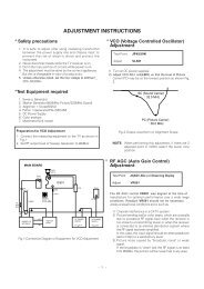
CHAPTER 2. ADJUSTMENTS<br />
[1] Adjustments<br />
General<br />
Since the following adjustments and settings are provided for this<br />
model, make adjustments and/or setup as necessary.<br />
1. Adjustments<br />
Adjustments of output voltage (FACTORY ONLY)<br />
1. Install the power supply unit in the machine.<br />
2. Set the recording paper and document.<br />
3. When the document is loaded, power is supplied to the output<br />
lines. Confirm that outputs are within the limits below.<br />
Output voltage settings<br />
CONTROL<br />
PWB<br />
CNPW<br />
Output Voltage limits<br />
+5V 4.75V~5.25V<br />
+12V 11.5V~12.5V<br />
VM (+24V) 23.04V~24.96V<br />
Fig. 1<br />
2. IC protectors replacement<br />
ICPs (IC Protectors) are installed to protect the TX motor drive circuit<br />
and verification stamp drive circuit. ICPs protect various ICs and electronic<br />
circuits from an overcurrent condition.<br />
The location of ICPs are shown below:<br />
CONTROL<br />
PWB<br />
(TOP SIDE)<br />
IC17<br />
F1<br />
IC13 F2 F3<br />
Fig. 2<br />
CNPW<br />
POWER SUPPLY<br />
PWB<br />
Connector<br />
No. CNPW<br />
Pin No.<br />
1 VM<br />
2 VM<br />
3 VM<br />
4 MG<br />
5 MG<br />
6 MG<br />
7 +5V<br />
8 +5V<br />
9 DG<br />
10 DG<br />
11 +12V<br />
12 AG<br />
CNPW CNPRT<br />
CNRS<br />
CNPN<br />
2 – 1<br />
(1) F3 (CCP2E20) is installed in order to protect IC’s from and<br />
overcurrent generated in the verification stamp drive circuit. If F3<br />
is open, replace it with a new one.<br />
(2) F1, F2 (CCP2E30) is installed in order to protect IC’s from an<br />
overcurrent generated in the TX motor drive circuit. If F1, F2 is<br />
open, replace it with a new one.<br />
In addition to the replacement of F1, F2 and F3, the factor<br />
causing F1, F2 and F3 to open must also be repaired. If not, F1,<br />
F2 and F3 will open again.<br />
Replacement parts<br />
CCP2E20 (Sharp code: VHVCCP2E20/-1)<br />
CCP2E30 (Sharp code: VHVCCP2E30/-1)<br />
3. Settings<br />
(1) Dial mode selector<br />
OPTION SETTING: DIAL MODE (Soft Switch No. SW2 DATA No. 1)<br />
Use this to set the fax machine to the type of telephone line you are<br />
on.<br />
• The factory setting is "TONE".<br />
(step 1) Select "OPTION SETTING".<br />
KEY:<br />
DISPLAY: TONE SELECTED<br />
KEY:<br />
FUNCTION 4<br />
DISPLAY: OPTION SETTING ENTER #01 33, ,#<br />
Cursor<br />
(step 2) Select "DIAL MODE".<br />
When initially registering,<br />
the mode shows 1=TONE.<br />
When registering again, the<br />
KEY: 2 3<br />
mode which was registered<br />
formerly is shown.<br />
DISPLAY: DIAL MODE 1=TONE, 2=PULSE<br />
(step 3) Select, using "1" or "2".<br />
KEY:<br />
KEY:<br />
DISPLAY:<br />
1<br />
2<br />
PULSE SELECTED<br />
(step 4) End, using the "STOP" key.<br />
STOP<br />
<strong>FO</strong>-<strong>4500</strong>H
<strong>FO</strong>-<strong>4500</strong>H<br />
[2] Diagnostics and service soft switch<br />
1. Operating procedure<br />
Two kinds of diagnoses are supported.<br />
1-1. Fax diagnosis<br />
This diagnosis is concerned with the main body of fax which is<br />
used for production and service support.<br />
Entering the diagnostic mode<br />
Press FUNC 9 8 7 , and the following<br />
display will appear.<br />
ROM: XXXXX XXXXX<br />
FBG0<br />
FBG1<br />
Then press the START key. Select the desired item with the key<br />
and the key or select with the rapid key.<br />
Enter the mode with the<br />
(Diag • specifications)<br />
START key.<br />
FUNC 9 8 7<br />
START<br />
01 START SOFT SWITCH MODE<br />
02 START PRINT AREA<br />
03 START ROM & RAM CHECK<br />
04 START AUTO FEEDER MODE<br />
05 START AGING MODE<br />
06 START PANEL CHECK MODE<br />
07 START OPTICAL ADJUST MODE<br />
08 START PRODUCT CHECK<br />
09 START SIGNAL SEND MODE<br />
10 START COMM. CHECK MODE<br />
11 START MEMORY CLEAR<br />
12 START FLASH MEMORY<br />
13 START ALL FAX/TEL ENTRY MODE<br />
14 START RS232C CHECK MODE<br />
15<br />
Identical<br />
START<br />
ROM: FBG0 FBG1<br />
DEPT. PASSCODE<br />
16 START CONF. PASSCODE<br />
17 START PRINT HOLD CODE<br />
18 START MEMORY SET MODE<br />
19 START MOTOR AGING<br />
20 START STAMP AGING<br />
21 START SCANNER SET MODE<br />
22 START DIAL TEST MODE<br />
23 START COPY DIAG MODE<br />
2 – 2<br />
1-2. Print diagnosis<br />
This diagnosis is concerned with the print which is used for production<br />
and service support.<br />
Entering the diagnostic mode<br />
Press FUNC 9 8 6 , and the following<br />
display will appear.<br />
PCU ROM Ver.:<br />
Then press the START key. Select the desired item with the<br />
key and the key or select with the rapid key.<br />
Enter the mode with the<br />
(Diag •specifications)<br />
START key.<br />
FUNC 9 8 6<br />
01 START AREA PRINT MODE<br />
02 START CHECK PATTERN 1<br />
03<br />
START<br />
CHECK PATTERN 2<br />
04 START CHECK PATTERN 3<br />
05<br />
06<br />
07<br />
08<br />
START<br />
START<br />
START<br />
START<br />
START<br />
PAPER FEED AGING<br />
BIAS ADJUST MODE<br />
LIFE SET MODE<br />
LIFE ALL CLEAR<br />
09 START LIFE ENTRY MODE<br />
10<br />
START<br />
PCU ROM Ver.:<br />
TOP ADJUST MODE<br />
11 START LIFE CLEAR MODE<br />
3) Memory clear when power is turned on<br />
Pressing the START and STOP keys, turn on the main power, and<br />
the following message will be displayed.<br />
MEMORY CLEAR<br />
EXECUTE ? 1 = YES 2 = NO<br />
Here, when 1: YES is selected, the memory will be cleared to be<br />
ready for operation.<br />
If 2: NO is selected, it will continue ready for operation as it is.
2. Diagnostic items description<br />
2-1. Fax diagnosis<br />
1) Soft switch mode<br />
In this mode, the soft switch are set and the soft switch list is printed.<br />
Soft switch mode screen<br />
1 Switch number selection<br />
• Press START key for setting of the next soft switch. If the soft switch<br />
number is the final, pressing START key will exit the soft switch<br />
mode.<br />
• Enter two digits of a soft switch number to set the switch number. If<br />
a switch number of unexisting soft switch is entered, key error<br />
buzzer sounds to reject the input.<br />
S O F T S W I T C H M O D E<br />
S W 0 1 = 0 0 0 0 0 0 0 0<br />
Soft switch mode screen<br />
S O F T S W I T C H M O D E<br />
S W 0 1 = 0 0 0 0 0 0 0 0<br />
Switch<br />
No.<br />
1 8<br />
Data<br />
S O F T S W I T C H M O D E<br />
S W 1<br />
1 6<br />
S O F T S W I T C H M O D E<br />
S W 1 6 = 0 0 0 1 0 1 1 0<br />
2 Data number selection<br />
The cursor position shows the data to be set.<br />
Pressing # key moves the cursor to the right. If, however, the cursor is<br />
on data number 8, pressing # key shifts the cursor to data number 1 of<br />
the next switch number. If the switch number is the final, pressing # key<br />
will exit the soft switch mode.<br />
Pressing key moves the cursor to the left. If, however, the cursor is<br />
on data number 1, pressing key shifts the cursor to data number 1<br />
of the former switch number. If the switch number is 1, pressing key<br />
will not move the cursor.<br />
3 Data setting method<br />
Press the FUNCTION key, and the data at the position of the cursor<br />
will be reversed to 0 when it is 1, or to 1 when it is 0. (If the soft switch<br />
can be changed at the bit (Refer to 6.), the error buzzer will sound<br />
with the process not received.)<br />
4 Outputting method of soft switch list<br />
In the soft switch mode, press the REPORT key, and the soft switch list<br />
will be output.<br />
If the recording paper runs out or is clogged, the key error buzzer will<br />
sound with the process not received.<br />
5 Storage of data<br />
In the following case, the data of the soft switches set will be stored.<br />
• It is shifted to set the next soft switch by pressing the START switch.<br />
• It is shifted to set the next soft switch with the [#] key.<br />
• It is shifted to set the last soft switch with the [ ] key.<br />
• It is shifted to set another soft switch by inputting two digits as the<br />
switch number. (When 2 digits are completely input.)<br />
• Output of the soft switch list is started.<br />
6 Inhibition of data change<br />
(This is also applicable for the optional setting.)<br />
In the following case, it is inhibited to change the data with the key<br />
error buzzer.<br />
• OFF to ON of telephone billing function which is using the image<br />
memory is used (Note: In the existing set, the telephone billing code<br />
function is specified from OFF to ON when the timer system communication<br />
(including the batch communication) is set.)<br />
Here, the memory is usable when the telephone billing code function<br />
is on. It can be set from ON to OFF while the memory is used.<br />
However, if setting is practically changed even once, it can not be<br />
returned from OFF to ON.<br />
• When the PC interface board is not mounted, [Switch of OFF → ON<br />
of the item of "PC interface function" and of FAX → PC of the item<br />
of "automatic receiving in the PC interface mode]<br />
(Note: This supports not only the operation protect of the optional<br />
setting and soft switch mode but also an example of the<br />
automatic compensation of soft switch to OFF/FAX when the<br />
power is turned on even if the PC PWB is removed when the<br />
optional setting and soft switch mode are set at ON/PC.)<br />
2 – 3<br />
(Though they are not provided, the existing model can operate<br />
without setting of the soft switch when it is not installed.)<br />
• OFF to ON of multi TTI function and telephone billing code function<br />
when the department control function is OFF.<br />
• OFF to ON of department control function during use of image<br />
memory.<br />
(Note: In the existing set, the department control function is set from<br />
OFF to ON when the timer communication (including the batch<br />
sending) or the memory hold is set.)<br />
• ON to OFF of continuous serial polling function when the continuous<br />
serial polling is started.<br />
(Note: In the existing set, "ON to OFF of the continuous serial<br />
polling function when the continuous serial polling is registered" has<br />
been applied, but the conditions are now moderated. However, registration<br />
is impossible to the program of the new continuous serial<br />
polling when the continuous serial polling function is OFF.)<br />
• In addition, change of all soft switches during communication<br />
7 Linked change of data (This is the same even in the optional setting.)<br />
• When the department control function is off, the multi TTI function<br />
and telephone billing code function are turned off.<br />
2) Print area<br />
According to the size of the specified sheet, the effective printing area is<br />
printed.<br />
3) ROM & RAM check<br />
The sum value of ROM, the work and the back-up RAM are checked.<br />
The RS232C interface is also checked. If any error occurs, the buzzer will<br />
inform it. (Refer to the following table). Finally, the result will be printed.<br />
This diagnosis does not check the flash memory. The flash memory is<br />
checked with the flash memory test.<br />
Number of buzzer sounds Device checked Remarks<br />
1 time ROM1 Main<br />
2 times ROM2 Main<br />
3 times Integrated ROM/RAM Main<br />
4 times D-RAM Main<br />
5 times S-RAM Main<br />
*6 times S-RAM (on the optional memory) Main<br />
* As practical, it is judged that the optional memory is not installed if any<br />
error occurs. Therefore, it does sometimes not sound.<br />
For the short and long sounds, one pattern is as follows.<br />
Main system: 0.25 seconds ON/0.25 seconds OFF<br />
Sub system: 1.00 second ON/0.25 seconds OFF<br />
The execution state of checking is as follows. Moreover, the list of the<br />
check result is output after checking is ended.<br />
Display during check Display after check<br />
ROM CPU SRAM DRM DPR ROM CPU SRAM DRM DPR<br />
• • • • • • • • • PP PP E PP P<br />
P=PASS E=ERROR<br />
<br />
ROM CPU SRAM DRM DPR<br />
• • • • • •<br />
DRAM (4Mbit)<br />
SRAM (256Kbit x 2)<br />
ROM (4Mbit x 2)<br />
• When the option is installed,<br />
two SRAMs are added every<br />
option.<br />
<strong>FO</strong>-<strong>4500</strong>H<br />
ROM/RAM<br />
check list<br />
output<br />
The check result of RS232C interface board is listed and printed together<br />
with the check result of ROM&RAM.
<strong>FO</strong>-<strong>4500</strong>H<br />
4) Auto feeder mode<br />
The auto feed function can be checked by inserting and discharging<br />
the document. (The distance between pages can be displayed during<br />
operation of the scanner.)<br />
1 Check of auto feed function<br />
After this mode is activated, set up the document, and press the<br />
START key, and it will be automatically fed. (Before the START<br />
key is pressed, the document sensor alone is activated.)<br />
Moreover, the document size (A4/B4) and sensor information<br />
(A4/B4/ORG) are displayed when the document sensor is turned.<br />
04 : AUTO FEEDER MODE<br />
( )<br />
After setup of the document<br />
04 : AUTO FEEDER MODE<br />
B4 (A4 B4 ORG)<br />
2 Display of distance between pages during operation of the scanner<br />
• Soon after this mode is c\activated, press the FUNCTION key<br />
for 5 seconds or more, and the display mode of the distance<br />
between pages will be activated. Then, set up the sending<br />
paper and select the image quality, and then press the START<br />
key, and operation will be started.<br />
Be sure to press the FUNCTION key prior to the START key. If<br />
the FUNCTION key is not pressed but the START key is<br />
pressed, it will operate in the same manner as in the existing<br />
auto feeder mode.<br />
If the START key is pressed, the FUNCTION key will be invalid<br />
hereafter. Therefore, the display mode of the distance between<br />
pages and the existing mode can not be changed.<br />
• While the sending paper is read, the image quality key can be<br />
input. STD/FINE/S-FINE modes are usable. However, the<br />
same operation of FINE will be selected if the intermediate tone<br />
is set.<br />
• The image quality, the length of the sending page read, the<br />
page distance to the next sending paper and the total of the<br />
sending papers read are shown on the display.<br />
• When the stop key is pressed or 100 sending papers are read,<br />
the content shown on the display will be totally output as the list<br />
after the remaining sending papers are discharged.<br />
5) Aging mode<br />
If any document is set up in the first state (when started), copying will<br />
be executed. If it is not set up, "check pattern 1" of the print diagnosis<br />
is output at the intervals of 1 time/60 minutes. (A total of 10 sheets<br />
are output.)<br />
6) Panel check mode<br />
Only the sensor which is<br />
activated (fallen down) is displayed.)<br />
The paper sheet size (A4/B4) is<br />
displayed.<br />
This is used to check whether each key is normally operated or not.<br />
According to the key input, LCD is displayed. Moreover, during execution,<br />
the document reading lamp is turned on.<br />
1 When [PANEL CHECK MODE] is displayed, press the [START]<br />
key.<br />
The test will be started. When the test is started, LED’s will sequentially<br />
come on. It is used to check all LED’s.<br />
2 Press any other key except [STOP] key.<br />
At this time, the name of each key will be displayed every push of<br />
the key.<br />
2 – 4<br />
3 However, if any key is pressed with the page plate opened, it will<br />
be equal to a press of key 32 with the page plate opened.<br />
4 Finally press the [STOP] key.<br />
If all keys can be input, the key input "ALL KEY OK!!" will be<br />
displayed when the STOP key is ended.<br />
The screen will be all displayed in black, and the test result will be<br />
printed.<br />
In this test, it is okayed if all the other keys except [STOP] key have<br />
been pressed from start of the test to its end (the [STOP] key is<br />
pressed). If any key is skipped, it will be regarded as "KEY ERROR!!",<br />
and the name of the key not pressed will be printed on the list as the<br />
result. This will complete printing.<br />
7) Optical adjust mode<br />
The document reading LED is turned on.<br />
8) Product check<br />
The diagnosis is used in the production process.<br />
After shift to the mode, the following operations are sequentially executed.<br />
At this time, the sensor of read-error can be checked by feeding<br />
the B3 document. Set up one short document of B4 size.<br />
1 Memory clear (Same as Diagnosis 11)<br />
2 Panel test (Same as Diagnosis 06)<br />
3 Dial test (Same as Diagnosis 22)<br />
4 Document feed<br />
5 Stamp press<br />
6 ROM & RAM test, RS232C interface board check (Same as the<br />
Diagnosis 03)<br />
7 Flash memory test mode (Same as Diagnosis 12)<br />
8 Registration of fixed data<br />
Registration of rapid key No. and other data necessary for production.<br />
The registered data are shown in the following table. The chain<br />
dial is not set for any destination.<br />
Rapid<br />
No.<br />
FAX<br />
No.<br />
Rapid<br />
No.<br />
FAX<br />
No.<br />
Rapid<br />
No.<br />
FAX<br />
No.<br />
Rapid<br />
No.<br />
FAX<br />
No.<br />
01 20 06 25 11 1 21 01<br />
02 21 07 26 12 2 22 02<br />
03 22 08 27 13 3 23 03<br />
04 23 09 28 14 4 24 04<br />
05 24 10 29 15 5 25 05<br />
9 Transmission check (Same as Diagnosis 10)<br />
The soft switches necessary for production are set.<br />
F Test result print (two sheets)<br />
• AUTO FEEDER CHECK LIST<br />
• FLASH MEMORY CHECK LIST<br />
Memory clear printing<br />
Panel test result printing<br />
ROM&RAM test result printing<br />
Check result printing of RS232C interface board<br />
G Print area printing (one sheet)
9) Signal send mode<br />
After shift to the mode, press the START key, and the signals will be<br />
transmitted in the following sequence.<br />
It can be used to check the modem and so on.<br />
[ 1] No signals<br />
[ 2] 4800BPS (V27ter)<br />
[ 3] 14400BPS (V. 33)<br />
[ 4] 12000BPS (V. 33)<br />
[ 5] 14400BPS (V. 17)<br />
[ 6] 12000BPS (V. 17)<br />
[ 7] 9600BPS (V. 17)<br />
[ 8] 7200BPS (V. 17)<br />
[ 9] 9600BPS (V. 29)<br />
[10] 7200BPS (V. 29)<br />
[11] 4800BPS (V27ter)<br />
[12] 2400BPS (V27ter)<br />
[13] 300BPS (FLAG)<br />
[14] 2100Hz (CED)<br />
[15] 1100Hz (CNG)<br />
10) Comm. check mode<br />
1 Turn on the line monitor.<br />
2 Bring the copy mode into the continuity mode.<br />
3 It is set to shift into the diagnosis mode when the SPEED key<br />
alone is pressed.<br />
After the check, it is necessary to be sure to return the aforementioned<br />
soft switches into the initial state.<br />
(Clear the memory with the diagnosis.)<br />
11) Memory clear<br />
Clear the back-up memory to initialize the soft switches.<br />
The flash memory will be initialized. Then, the initialized list be output.<br />
12) Flash memory<br />
The flash memory is checked.<br />
The ordinary memories (ROM, SRAM, DRAM) are checked in the<br />
ROM&RAM check process. The write/read test is taken every block to<br />
print the result.<br />
When an error occurs, the following error buzzer will sound.<br />
Number of buzzer sounds Check device<br />
7 times Page memory<br />
8 times Flash memory<br />
9 times Flash memory (optional)<br />
During operation of this diagnosis, dual operation is not possible at<br />
all.<br />
If this is excessively repeated, it will shorten the life of the flash<br />
memory.<br />
13) All FAX/TEL. entry mode<br />
Before entry into the diagnosis, the reference destination number is<br />
first written into the Rapid key number 01 in the FAX number registration<br />
mode.<br />
1 The diagnosis mode is activated. If any number is not registered in<br />
the Rapid key number 01 or any program or group is registered,<br />
the diagnosis will be passed without any execution.<br />
2 The FAX/TEL No. (including the substitutive one) of the Rapid key<br />
number 01 is copied into the Rapid key numbers 02 thru 48.<br />
2 – 5<br />
3 The FAX number of the Rapid key number 01 is copied into the<br />
speed key numbers 001 thru 100.<br />
4 If any chain dial is not set in the Rapid key number 01, the Rapid<br />
key number 02 thru 48 and speed key numbers 001 thru 100 are<br />
registered in the group number.<br />
If any chain dial is set, any group will not be produced but the<br />
chain dial setting alone of the Rapid dial will be canceled.<br />
(In all others Rapid key numbers except 01, the chain dial is kept<br />
as it is set.)<br />
(16th and subsequential letters of the destination name registered in<br />
the Rapid No. 01 will be discarded.)<br />
14) RS232C check mode<br />
RS232C interface board is checked.<br />
When the interface board is installed, the result will be printed after<br />
the check.<br />
It is not installed, the following will be displayed.<br />
14: RS232C CHECK MODE<br />
I/F PWB NOT CONNECT<br />
The process will be ended after sounding of the error end buzzer.<br />
15) Dept. passcode<br />
The department passcode list is printed.<br />
16) Conf. passcode<br />
The confidential passcode list is printed.<br />
Differing from printing of one box alone soon after registration, the<br />
confidential passcodes of all boxes are printed.<br />
17) Print hold code<br />
The print lockout passcode No. is printed.<br />
<strong>FO</strong>-<strong>4500</strong>H<br />
18) Memory set mode<br />
The set and dump list of the memory content is output.<br />
• The address (8 digits (P) generally including the bank information<br />
is input, and the data of 2 digits is continuously input.<br />
Inputting is done in the hexadecimal mode. The ten-key is used for<br />
0 thru 9, and the alphabetic keys A (RAPID01 thru 06) are used for<br />
A thru F.<br />
• During data inputting, the address can be moved forward and<br />
backward one byte by one byte with " " and "#". (The address<br />
prior to the address 0 is looped as the maximum address.)<br />
• The Validity of the address is not checked. Accordingly, writing/reading<br />
operations are possible in the address of the memory<br />
not assigned, the address of ROM and so on.<br />
(However, as practical, writing is not done, and the data content<br />
runs short each reading.)<br />
Though writing is possible in the flash memory, a little time is<br />
required.<br />
It is also necessary to take care that the life of the flash memory is<br />
excessively shortened if much data is written in the flash memory.<br />
Since it may run away depending the written content, take minute<br />
care for the writing address.<br />
• When the REPORT key is input, the memory dump list is produced<br />
from the displayed address (here, it is limited at the 16-byte boundary<br />
address (address with end 0) which does not exceed the specified<br />
address and is just in front.). The dump list is output to a<br />
maximum of 99 pages. If any data of one page can be repeatedly<br />
developed and printed, the list is sufficient. But it is not desired that<br />
the content of plural pages are developed in the memory once and<br />
are then printed. If the STOP key is pressed, it will pass to the<br />
diagnosis after the page which is now being printed is completed<br />
printed.<br />
If the address exceeds the maximum address, it will return to the<br />
address 0 and printing will be continued.
<strong>FO</strong>-<strong>4500</strong>H<br />
19) Motor aging<br />
• Whether a document is present or not, the motor in the sending<br />
system is kept in rotation until the STOP key is pressed.<br />
• The image quality selection key can be input during stop alone to<br />
set the rotation speed for the image quality.<br />
(Here, the speed for FINE is selected when the intermediate tone<br />
is specified.)<br />
• The image quality for default at the start of execution is STD<br />
regardless of the image quality selection priority of the main body.<br />
• For rotation, the key "1" selects the 1-2 phase excitation, "2"<br />
selects the 2-phase excitation and "3" selects the micro step. It can<br />
not be changed during rotation. The 1-2 phase excitation is set as<br />
default.<br />
20) Stamp aging<br />
• It is impossible if any document is not set up.<br />
• The document is fed at the 10 mm intervals, and is continuously<br />
stamped.<br />
• The total number of stamps from entry of the mode is displayed on<br />
the screen.<br />
• The ordinary operation aging which stamps a finish every document<br />
is executed in the ordinary copying mode.<br />
21) Scanner set mode<br />
• The reading width and motor drive conditions are set.<br />
<br />
1. Top margin<br />
2. Bottom margin<br />
3. Left adjustment (The left position alone is specified.)<br />
Specify the above values.<br />
• Select the above items 1, 2 and 3 with the [ ] and [#] keys, and<br />
set the values with the [←] and [→] keys. The values can be set in<br />
the range of +3.0 mm to -3.0 mm at the 0.1 mm intervals. While<br />
the [←] and [→] key is continuously pressed one second or more,<br />
the setting value is automatically increased/decreased (in the<br />
range between the upper and lower limits).<br />
• Input the quality selection key, and the value will be respectively<br />
set corresponding to the selected image quality. Here, the intermediate<br />
tone is the same as for the setting value of FINE.<br />
• ±0.0 mm is default for all.<br />
<br />
4. Motor<br />
5. Phase<br />
6. Slow-up<br />
7. Slow-down<br />
Specify the above values.<br />
• Select the above items 4 thru 7 with the [ ] and [#] keys, and<br />
select the setting value with the ten-key.<br />
Setting values<br />
4. 6 steps<br />
5. Selection of one mode from 1-2 phase, 2-phase and micro step<br />
6. 3 steps<br />
7. 3 steps<br />
• Input the quality selection key, and the value will be respectively<br />
set corresponding to the selected image quality. Here, the intermediate<br />
tone is the same as for the setting value of FINE.<br />
1. TOP<br />
2. BOTTOM<br />
3. LEFT<br />
4. MOTOR<br />
5. PHASE<br />
6. SLOW UP<br />
7. SLOW DOWN<br />
2 – 6<br />
22) Dial test mode<br />
The mode is used to inspect whether dialing is accurate in two kinds<br />
of dial modes . All data which can be dialed in this mode are<br />
automatically called up in both PB mode and DP mode.<br />
When this mode is activated, the following operations will be automatically<br />
executed . Whether the dialed content is right or not is judged<br />
with the external instrument which is connected to the line cable.<br />
1 After shift to the FAX diagnosis mode, press RAPID 24.<br />
(Also switch the display with the [ ] and [#] keys.)<br />
2 Press the START key.<br />
3 Turn on CML, and dial the following in the PB mode.<br />
1, 2, 3, 4, 5, 6, 7, 8, 9, , 0, #<br />
4 Turn off CML 500 mS alone.<br />
5 Dial the following in the DP mode.<br />
1, 5, 9, 0<br />
6 After dialing, turn off CML.<br />
This mode uses the ordinary auto dial. (Accordingly, the signal sending<br />
time and minimum pause are all the same as ordinary.<br />
The measurement result in this mode is completely all the same as in<br />
the ordinary dial mode.<br />
Moreover, the same process as above is also done in the dial test<br />
mode which is executed in the product check mode.<br />
23) Copy diag mode<br />
In order to shorten the process time during production, this mode is<br />
used to automatically switch the copy mode. Three menus are provided.<br />
1. 1 Set up two documents. (In case of two documents or more,<br />
there is no problem.<br />
2 Press the START key.<br />
3 Copy 1st document in the fine mode/density AUTO. (One<br />
sheet is printed in the ordinary copy mode.)<br />
4 Copy 2nd (subsequential) document in the intermediate<br />
tone mode/density DARK. (In the ordinary copying mode,<br />
one sheet is printed when the RESOLUTION key is pressed<br />
three times.)<br />
When copy test is tried during production or is checked in two modes<br />
(fine and intermediate tones), this mode is provided to reduce the<br />
troublesome work which makes the operator stand aside to change<br />
the mode. Accordingly, the fine and intermediate tones are merely<br />
switched, and the mode is not switched to another mode. (Input of the<br />
image quality/density key is invalid.)<br />
2. Try the copy in the mode fixed at COPY REDUCE 95% and<br />
fine mode/density AUTO. At this time, don’t change the soft<br />
key of COPY REDUCE. (Input of the image quality/density key<br />
is invalid.<br />
3. Continuously try the above items 1 and 2.
2-2. Print diagnosis<br />
Rapid key 01: Area print mode<br />
The effective printing area frame is printed in the specified sheet size.<br />
1. [Full black pattern]<br />
2. [Intermediate tone 2 pattern]<br />
3. [Intermediate tone 1 pattern]<br />
4. [Mesh point pattern]<br />
1. Full Black pattern<br />
2. Intermediate tone 2 pattern<br />
3. Intermediate tone 1 pattern<br />
4. Mesh point pattern<br />
5. Longitudinal strip 2 pattern<br />
6. Lateral strip 2 pattern<br />
7. Longitudinal strip 1 pattern<br />
8. Lateral strip 1 pattern<br />
9. Full white pattern<br />
4mm ± 2<br />
208mm<br />
4mm<br />
4mm ± 2.5<br />
pattern is repeated.<br />
5mm<br />
The left pattern is repeated.<br />
5. [Longitudinal strip 2 pattern]<br />
Black 2 dot and white 2 dot are repeated in line.<br />
6. [Lateral strip 2 pattern]<br />
Black 2 line and white 2 line are repeated.<br />
7. [Longitudinal strip 1 pattern]<br />
Black 1 dot and white 1 dot are repeated in line.<br />
8. [Lateral strip 1 pattern]<br />
Black 1 line and white 1 line are repeated.<br />
9. [Full White pattern]<br />
Rapid key 02: Check pattern 1<br />
The lateral stripe 2 pattern is printed on one sheet.<br />
(Black 2 line and white 2 line are repeated.)<br />
Rapid key 03: Check pattern 2<br />
The lateral stripe 2 pattern is printed on multiple pages.<br />
Press the STOP key to end the printing.<br />
Rapid key 04: Check pattern 3<br />
The intermediate tone 1 is printed on one sheet.<br />
The left pattern is repeated.<br />
The left pattern is repeated.<br />
2 – 7<br />
Rapid key 05: Paper feed aging<br />
The mode is used for aging related to the printing. In this mode, the<br />
following modes are provided.<br />
1 Blank paper aging mode (ALL WHITE AGING)<br />
2 Whole black print aging mode (ALL BLACK AGING)<br />
3 5% printing aging mode (5% AGING)<br />
4 4% printing aging mode (4% AGING)<br />
After selecting the paper-pass aging mode in the print diagnosis mode,<br />
input the number of each mode above with the ten-key, and the mode will<br />
be executed. The detailed specifications of each mode are described as<br />
follows. Here, the operation in each mode is stopped only when the STOP<br />
key is pressed by the operator or a printing-impossible error occurs.<br />
• Blank paper aging mode<br />
In the mode, printing is continued in the whole white (white paper) printing<br />
pattern until the STOP key is pressed by the operator. (In the printing area)<br />
• Whole black printing aging mode<br />
In the mode, printing is continued in the whole black (whole black) printing<br />
pattern until the STOP key is pressed by the operator. (In the printing area)<br />
Rapid key 6: Bias adjust mode<br />
The mode is used to adjust the printing density of the printed image. The<br />
image printing density is adjustable in six steps of 1 to 6.<br />
For details, refer to the following table. (For selection, use the keys 1 thru<br />
6.)<br />
Image printing density Thin ← → Thick<br />
1 2 3 4 5 6<br />
Default value O<br />
Rapid key 7: Life set mode<br />
The mode is used to set the life counter of the printer and the counter of<br />
the auto feeder at desired values. For setting, proceed with the following<br />
procedure.<br />
1 When the life counter setting mode is selected, the following will be is<br />
displayed.<br />
# key<br />
M A C H I N E<br />
D R U M<br />
L I F E = 0 0 0 1 2 3<br />
L I F E = 0 0 0 1 2 3<br />
L I F E 1 = 0 0 0 1 2 3<br />
L I F E 2 = 0 0 0 1 2 3<br />
L I F E 3 = 0 0 0 1 2 3<br />
F E E D E R L I F E = 0 0 0 1 2 3<br />
T O N E R L I F E = 0 0 0 1 2 3<br />
<strong>FO</strong>-<strong>4500</strong>H<br />
The cursor blinks at the top data.<br />
Seven counters can be selected with the "#" and " " keys.<br />
2 In the state 1, input a desired setting number of 6 digits with the<br />
ten-key.<br />
3 After input of 6 digits, shift to another counter with the "#" and " "<br />
keys as necessary. When all necessary counters are completely<br />
input, press the START key.<br />
4 "STORED" will be displayed with the set values stored into the<br />
memory. For checking, retry this mode.<br />
Note:<br />
The counter shows the operational state of the printer (how many<br />
sheets have been printed since start of use? and others). The ordinary<br />
memory does not reset the counter. For clearing, set 0 in this<br />
mode or use the life counter clear mode in Item 3-9. (Accordingly, it is<br />
necessary to reset the counter or do the clear process in addition to<br />
the ordinary memory clear if the content in the memory on the control<br />
PWB is broken because of PWB repair, etc. (In the production stage,<br />
it is necessary to execute this in the last process.)<br />
key
<strong>FO</strong>-<strong>4500</strong>H<br />
Rapid key 08: Life all clear<br />
The mode is used to clear the life counter of the printer of the counter<br />
of the auto feeder.<br />
Note: The counter shows the operational state of the printer (e.g.<br />
how many sheets have been printed since start of use?). The<br />
ordinary memory does not reset the counter. For clearing, set<br />
0 in the mode 8 or execute this mode. (Accordingly, it is necessary<br />
to reset this counter in addition to the ordinary memory<br />
clear if the content in the memory on the control PWB is<br />
broken because of PWB repair, etc. (In the production stage, it<br />
is necessary to execute this in the last process.)<br />
Rapid key 09: Life entry mode<br />
(For Serviceman temporary counter)<br />
The mode is used to set a desired value for the judgment value<br />
(alarm judgment counter value) of the general purpose life counters 1<br />
thru 3 of the printer. If the life of a consumable part (developer,<br />
imprinter, etc) is set, the model which has the error display and RMS<br />
function will inform RMS when the counter reaches the set value.<br />
For setting, proceed with the following procedure.<br />
1 When the life counter setting mode is selected, the following will<br />
be displayed.<br />
L I F E 1 = 0 0 0 0 0 0<br />
# key L I F E 2 = 0 0 0 0 0 0<br />
key<br />
L I F E 3 = 0 0 0 0 0 0<br />
The cursor blinks at the top data.<br />
Three counters can be selected with the "#" and " " keys.<br />
2 In the state 1, input a desired setting number of 6 digits with the<br />
ten-key.<br />
3 After input of 6 digits, shift to another counter with the "#" and " "<br />
keys as necessary. When all necessary counters are completely<br />
input, press the START key.<br />
4 "STORED" will be displayed with the set values stored into the<br />
memory. For checking, retry this mode.<br />
Note: The counter shows the operational state of the printer (how<br />
many sheets have been printed since start of use? and others).<br />
The ordinary memory does not reset the counter. For<br />
clearing, set 0 in this mode or use the life counter clear mode<br />
in Item 3-9. (Accordingly, it is necessary to reset the counter or<br />
do the clear process in addition to the ordinary memory clear if<br />
the content in the memory on the control PWB is broken because<br />
of PWB repair, etc. (In the production stage, it is necessary<br />
to execute this in the last process.)<br />
Rapid key 10: Top adjust mode<br />
As the method to adjust the top margin for printing, adjust top-margin<br />
adjusting VR on the PWB. If this mode is used at this time, adjustment<br />
is possible without the printing test every time when VR is<br />
turned.<br />
For the practical use, determine the adjusting value on the basis of<br />
the old data, and adjust to the determined value in this mode. Then,<br />
check it with the printing test.<br />
2 – 8<br />
Rapid key 11: Life clear mode<br />
The mode is used to respectively clear the life counter of the printer<br />
and the counter of the auto feeder. For setting, proceed with the<br />
following procedure.<br />
1 When the life counter clearing mode is selected, the following will<br />
be is displayed.<br />
Seven counters can be selected with the "#" and " " keys.<br />
# key<br />
M A C H I N E<br />
D R U M<br />
L<br />
L I F E<br />
L I F E<br />
I F E 1<br />
C L E A R<br />
C L E A R<br />
C L E A R<br />
L I F E 2 C L E A R<br />
L I F E 3 C L E A R<br />
F E E D E R L I F E C L E A R<br />
T O N E R L I F E C L E A R<br />
2 In the state 1, input the CLEAR key, and the counter will be<br />
respectively cleared.<br />
3 After one clear, move the cursor to another counter with the "#"<br />
and " " keys as necessary, and then press the CLEAR key.<br />
When the necessary counters are completely cleared, press the<br />
STOP key.<br />
key
3. How to make soft switch setting<br />
To enter the softswitch mode, make the following key entries in sequence.<br />
Press FUNCTION 9 8 7 START 0 1 START<br />
S F T S W 1 = 0 0 0 0 0 0 0 0<br />
S F T S W 1 = 1 0 0 0 0 0 0 0<br />
S F T S W 1 = 1 0 0 0 0 0 0 0<br />
S F T S W 1 = 1 0 0 0 0 0 0 0<br />
S F T S W 1 = 1 0 0 0 0 0 0 0<br />
S F T S W 2 = 0 0 0 0 0 0 0 0<br />
S F T S W 99 = 0 0 0 0 0 0 0 0<br />
The soft switch mode is terminated.<br />
2 – 9<br />
Press FUNCTION key.<br />
Press key.<br />
Press key.<br />
Bit1 - 8 are set.<br />
Press START key during setting.<br />
Soft SW2 - 99 are set.<br />
To finish the settings halfway between<br />
SW 1 and SW99, press the STOP key.<br />
In this case, the setting being done to<br />
the SW No. on display will be nullified<br />
while settings done to the preceding<br />
SW Nos. remain in effect.<br />
<strong>FO</strong>-<strong>4500</strong>H
<strong>FO</strong>-<strong>4500</strong>H<br />
4. Soft switch description<br />
• Soft switch<br />
SW<br />
NO.<br />
DATA<br />
NO.<br />
ITEM<br />
Switch setting and function<br />
1 0<br />
Initial<br />
setting<br />
Remarks<br />
1 Recall interval Binary input 8 4 2 1 0 OPTION<br />
2 No. = 1 2 3 4 (Data No.) 1 Set to 1 ~ 15<br />
3 EX 0 1 0 1 0<br />
SW1 4 eg. Recall interval is set to 5 min. 1<br />
5 Recall attempts Binary input 8 4 2 1 0 OPTION<br />
6 No. = 5 6 7 8 (Data No.) 0<br />
7 EX 0 0 1 0 1 Set to 1 ~ 15<br />
8 eg. Recall attempt times is set to 2 times. 0<br />
1 Dialing mode PULSE TONE 0<br />
2 Receive mode AUTO <strong>MANUAL</strong> 1<br />
3 ECM mode Off On 0 OPTION<br />
SW2 4 Reserved 0<br />
5 Polling security On Off 1 OPTION<br />
6 Auto cover sheet No Yes 1 OPTION<br />
7 JUNK-FAX function in manual reception Yes No 0<br />
8 JUNK-FAX function Yes No 0 OPTION<br />
1 Number of rings for auto-receive<br />
Binary input 8 4 2 1 0 OPTION<br />
2 (0: No ring receive)<br />
No. = 1 2 3 4 (Data No.) 0 Set to 0~15<br />
3 EX 0 0 0 1 0<br />
SW3 4 eg. Number of rings for auto receive is set to 1. 1<br />
5 Switch to auto-receive from manual receive Binary input 8 4 2 1 0 OPTION<br />
6 (0: No switch)<br />
No. = 5 6 7 8 (Data No.) 0 Set to 0~15<br />
7 EX 0 0 0 0 0<br />
8 eg. Switch to auto receive is set to disable. 0<br />
Communication results printout Printed at Printed at Printed at Not printed Printed<br />
OPTION<br />
error only error/timer/ transmis-<br />
every time<br />
memory sion mode<br />
only only<br />
1 No. 1 0 0 0 1 1 0<br />
2 No. 2 0 0 1 0 1 1<br />
SW4<br />
3 No. 3 1 0 0 0 0 0<br />
4 Image addition function to the communication<br />
result table (for memory transmission only)<br />
On Off 1 OPTION<br />
5 Reserved 0<br />
6 Reserved 0<br />
7 Reserved 1<br />
8 Multi-TTI feature On Off 0 OPTION<br />
1 Time display format 24 hours 12 hours-AM/PM 1<br />
2 Date display format Month-Day-Year Day-Month-Year 0<br />
3 Header print Off On 0<br />
SW5<br />
4<br />
5<br />
Footer print<br />
Relay data output<br />
On<br />
No<br />
Off<br />
Yes<br />
1<br />
0<br />
6 Substitute reception Off On 0<br />
7 Substitute reception conditions Reception disable without Reception enable without 0<br />
TSI<br />
TSI<br />
8 CSI transmission Off On 0<br />
2 – 10
SW<br />
NO.<br />
SW6<br />
SW7<br />
SW8<br />
DATA<br />
NO.<br />
ITEM<br />
Switch setting and function Initial<br />
1 0<br />
setting<br />
Remarks<br />
1 MH fixed Yes No (depend on remote machine) 0<br />
2 H2 mode No Yes 0<br />
3 Reserved 0<br />
Modem speed<br />
V. 17 V. 29 V. 27ter Except left<br />
4<br />
(DCS data reception speed)<br />
No. 4<br />
14400 12000 9600 7200<br />
0 0 0 0<br />
9600<br />
0<br />
7200<br />
0<br />
4800<br />
0<br />
2400<br />
0 0<br />
table, work to<br />
default.<br />
5 No. 5 1 1 1 1 0 0 0 0 1<br />
6 No. 6 0 0 0 0 0 0 0 0 0<br />
7 No. 7 0 1 0 1 0 1 1 0 0<br />
8 No. 8 0 0 1 1 1 1 0 0 0<br />
Reception speed fixed NO V. 17-<br />
14400BPS<br />
V. 29-<br />
9600BPS<br />
V. 27ter-<br />
4800BPS<br />
<strong>FO</strong>-<strong>4500</strong>H<br />
When 14400BPS<br />
MODEM used,<br />
setting to<br />
14400BPS is<br />
ignore.<br />
1 No. 1 0 1 0 1 0<br />
2<br />
No. 2 0 1 1 0<br />
0<br />
3 DIS receive acknowledge in G3 Twice Once in NSF reception, twice in 0 Effective to<br />
transmission<br />
DIS reception<br />
international<br />
comm.<br />
4 Non-modulated carrier in V.29<br />
transmission mode<br />
On Off 1<br />
5 EOL detection timer 25sec 5sec 0<br />
6 Protocol monitor On Off 0<br />
7 Line monitor On Off 0<br />
8 Max. length for TX/RX/Copy TX: 432mm, RX: unlimited TX/Copy: 432mm, RX: 1.5m 0<br />
Compromise Equalizer 0Km 1.8Km 3.6Km 7.2Km Valid when<br />
1 No. 1 0 0 1 1 0 transmitting<br />
2 No. 2 0 1 0 1 1<br />
3 Reserved 0<br />
4 Pause time 2sec (1sec from the second pause) 4sec (2sec from the second pause) 0<br />
5 Signal transmission level Binary input 8 4 2 1 1<br />
6 No. = 5 6 7 8 (Data No.) 0<br />
7 EX 1 0 1 1 1<br />
8 Set to -(n+3)dBm<br />
eg. Signal transmission level is set to -11dBm<br />
1<br />
2 – 11
<strong>FO</strong>-<strong>4500</strong>H<br />
SW<br />
NO.<br />
SW9<br />
SW10<br />
SW11<br />
SW12<br />
SW13<br />
SW14<br />
DATA<br />
NO.<br />
ITEM<br />
Switch setting and function Initial<br />
1 0<br />
setting<br />
1 CED tone signal interval 500ms 75ms 1<br />
2 CI signal OFF detect enable time 350ms or more 700ms or more 0<br />
3 Equalizer freeze On Off 0<br />
4 Equalizer freeze conditions All 7200bps 0<br />
5 Reserved 0<br />
6 CED detection time 1000ms 2000ms 0<br />
7 Reserved 0<br />
8 Reserved 0<br />
1 Reserved 0<br />
2 Reserved 0<br />
3 Reserved 0<br />
4 Reserved 0<br />
5 Reserved 0<br />
6 Reserved 0<br />
7 Reserved 0<br />
8 Reserved 0<br />
Remarks<br />
1 Memory retransmission times Binary input 8 4 2 1 0 OPTION<br />
2 No. = 1 2 3 4 (Data No.) 0<br />
3 EX 0 0 1 0 1<br />
4 eg. Retransmission time set to 10 times. 0<br />
5 Memory retransmission interval Binary input 8 4 2 1 0 OPTION<br />
6 No. = 5 6 7 8 (Data No.) 1<br />
7 EX 0 1 0 1 0<br />
8 eg. Retransmission interval set to 5 min. 1<br />
1 Reserved 0<br />
2 Reserved 0<br />
Alarm buzzer 3sec 1sec No BEEP No BEEP<br />
3 No. 3 0 0 1 1 0<br />
4 No. 4 0 1 0 1 0<br />
5 Action when RTN received Handle to no error Handle to error 1<br />
6 Reserved 0<br />
7 Reserved 0<br />
8 Reserved 0<br />
1 Reserved 0<br />
2 Reserved 0<br />
3 Reserved 0<br />
4 Reserved 0<br />
5 Reserved 0<br />
6 Reserved 0<br />
7 Reserved 0<br />
8 Reserved 0<br />
1 Reserved 0<br />
2 Reserved 1<br />
3 Reserved 0<br />
4 Reserved 1<br />
5 Reserved 0<br />
6 Reserved 0<br />
7 Reserved 1<br />
8 Reserved 0<br />
2 – 12
SW<br />
NO.<br />
SW15<br />
SW16<br />
SW17<br />
SW18<br />
SW19<br />
SW20<br />
DATA<br />
NO.<br />
ITEM<br />
Switch setting and function Initial<br />
1 0<br />
setting<br />
1 Reserved 0<br />
2 Reserved 1<br />
3 Reserved 0<br />
4 Reserved 0<br />
5 Reserved 1<br />
6 Reserved 1<br />
7 Reserved 0<br />
8 Reserved 0<br />
1 Reserved 0<br />
2 Reserved 0<br />
3 Reserved 0<br />
4 Reserved 1<br />
5 Reserved 0<br />
6 Reserved 0<br />
7 Reserved 0<br />
8 Reserved 0<br />
1 Reserved 0<br />
2 Reserved 1<br />
3 Reserved 0<br />
4 Reserved 1<br />
5 Reserved 0<br />
6 Reserved 0<br />
7 Reserved 1<br />
8 Reserved 0<br />
1 Reserved 1<br />
2 Reserved 0<br />
3 Reserved 0<br />
4 Reserved 1<br />
5 Reserved 0<br />
6 Reserved 0<br />
7 Reserved 0<br />
8 Reserved 0<br />
1 Reserved 0<br />
2 Reserved 0<br />
3 Reserved 0<br />
4 Reserved 0<br />
5 Reserved 1<br />
6 Reserved 0<br />
7 Reserved 0<br />
8 Reserved 0<br />
1 Reserved 0<br />
2 Reserved 0<br />
3 Reserved 0<br />
4 Reserved 1<br />
5 Reserved 0<br />
6 Reserved 0<br />
7 Reserved 0<br />
8 Reserved 0<br />
2 – 13<br />
<strong>FO</strong>-<strong>4500</strong>H<br />
Remarks
<strong>FO</strong>-<strong>4500</strong>H<br />
SW<br />
NO.<br />
SW21<br />
SW22<br />
SW23<br />
SW24<br />
SW25<br />
SW26<br />
DATA<br />
NO.<br />
ITEM<br />
Switch setting and function Initial<br />
1 0<br />
setting<br />
1 Reserved 0<br />
2 Reserved 1<br />
3 Reserved 0<br />
4 Reserved 0<br />
5 Reserved 1<br />
6 Reserved 0<br />
7 Reserved 1<br />
8 Reserved 1<br />
1 Reserved 1<br />
2 Reserved 0<br />
3 Reserved 0<br />
4 Reserved 0<br />
5 Reserved 0<br />
6 Reserved 0<br />
7 Reserved 0<br />
8 Reserved 0<br />
1 Reserved 0<br />
2 Reserved 0<br />
3 Reserved 0<br />
4 Reserved 0<br />
5 Reserved 0<br />
6 Reserved 0<br />
7 Reserved 0<br />
8 Reserved 0<br />
1 Reserved 0<br />
2 Reserved 0<br />
3 Reserved 1<br />
4 Reserved 0<br />
5 Reserved 0<br />
6 Reserved 1<br />
7 Reserved 0<br />
8 Reserved 1<br />
1 Reserved 0<br />
2 Reserved 0<br />
3 Reserved 0<br />
4 Reserved 0<br />
5 Reserved 1<br />
6 Reserved 0<br />
7 Reserved 0<br />
8 Reserved 0<br />
1 Reserved 0<br />
2 Reserved 0<br />
3 Reserved 0<br />
4 Reserved 0<br />
5 Reserved 0<br />
6 Reserved 0<br />
7 Reserved 0<br />
8 Reserved 0<br />
2 – 14<br />
Remarks
SW<br />
NO.<br />
SW27<br />
SW28<br />
SW29<br />
SW30<br />
SW31<br />
DATA<br />
NO.<br />
ITEM<br />
Switch setting and function Initial<br />
1 0<br />
setting<br />
Remarks<br />
1 Reserved 0<br />
2 Reserved 0<br />
3 Verification STAMP Yes No 0 Invalid if not<br />
mounted.<br />
4 Reserved 0<br />
Key buzzer volume Off HIGH MIDDLE LOW<br />
5 No. 5 0 0 1 1 1<br />
6 No. 6 0 1 0 1 1<br />
7 Reserved 0<br />
8 Reserved 0<br />
Speaker volume HIGH HIGH MIDDLE LOW<br />
1 No. 1 0 0 1 1 1<br />
2 No. 2 0 1 0 1 1<br />
3 Reserved 1<br />
4 Reserved 0<br />
Ringer volume Off HIGH MIDDLE LOW<br />
5 No. 5 0 0 1 1 1<br />
6 No. 6 0 1 0 1 1<br />
7 Reserved 0<br />
8 Reserved 0<br />
1 Reserved 0<br />
2 PC I/F mode On Off 0 OPTION<br />
3 Auto receive with PC I/F PC FAX 0 OPTION<br />
4 Reserved 0<br />
5 Reserved 0<br />
6 Reserved 0<br />
7 Reserved 0<br />
8 Reserved 0<br />
1 Resistration of header Disabled Enabled 0<br />
2 Reserved 0<br />
3 Reserved 0<br />
4 Reserved 0<br />
5 Reserved 0<br />
6 Reserved 0<br />
7 Reserved 0<br />
8 Quick on-line Yes No 1<br />
1 Reserved 0<br />
2 Reserved 0<br />
3 Reserved 0<br />
4 Reserved 0<br />
5 Reserved 1<br />
6 Reserved 0<br />
7 Reserved 1<br />
8 Reserved 0<br />
2 – 15<br />
<strong>FO</strong>-<strong>4500</strong>H
<strong>FO</strong>-<strong>4500</strong>H<br />
SW<br />
NO.<br />
SW32<br />
SW33<br />
SW34<br />
SW35<br />
SW36<br />
DATA<br />
NO.<br />
ITEM<br />
Switch setting and function<br />
1 0<br />
Initial<br />
setting<br />
Remarks<br />
1 Print hold On Off 0 OPTION<br />
2 Reserved 0<br />
3 Reserved 0<br />
4 Changeover of print cassette On Off 1 OPTION<br />
Selection of print cassette<br />
Single Auto. T→C C→T<br />
Indicate of<br />
(when single cassette)<br />
cassette<br />
Work in auto mode<br />
priority<br />
5 No. 5 0 1 0 except in this table. 0 T...TRAY<br />
6 No. 6 0 0 1 0 C...CASSETTE<br />
7 No. 7 0 0 0 0<br />
8 No. 8 0 1 1 0<br />
Heater mode Always on Always off Off timer OPTION<br />
1 No. 1 0 0 1 0<br />
2 No. 2 0 1 0 1<br />
Density adjustment of print bias Binary input 4 2 1 set to 1~6.<br />
3<br />
4<br />
5<br />
No. = 3 4 5 (Data No.)<br />
EX 1 0 0<br />
eg. Bias is set to level 4.<br />
1: faint 6: deep 0<br />
1<br />
1<br />
set to 0,7 is<br />
equal to 4<br />
(100).<br />
6 Limit value of drum life 0 near = 19,000 pcs. 0 near = 15,000 pcs.<br />
1 near = 15,000 pcs. 1 near = 16,000 pcs.<br />
0<br />
7 0 limit = 20,000 pcs. 1 limit = 16,000 pcs.<br />
0 limit = 20,000 pcs. 1 limit = 20,000 pcs.<br />
0<br />
8 Reserved 0<br />
1 Start time of heater OFF timer<br />
Binary input 8 4 2 1 0 OPTION<br />
2 (Upper digit of hour)<br />
No. = 1 2 3 4 (Data No.) 0<br />
3 EX 0 0 0 0 0<br />
4 0<br />
5 Start time of heater OFF timer<br />
Binary input 8 4 2 1 0 OPTION<br />
6 (Lower digit of hour)<br />
No. = 5 6 7 8 (Data No.) 0<br />
7 EX 0 0 0 0 0<br />
8 eg. Start time is set to 15: XX 0<br />
1 Start time of heater OFF timer<br />
Binary input 8 4 2 1 0 OPTION<br />
2 (Upper digit of minute)<br />
No. = 1 2 3 4 (Data No.) 0<br />
3 EX 0 0 0 0 0<br />
4 0<br />
5 Start time of heater OFF timer<br />
Binary input 8 4 2 1 0 OPTION<br />
6 (Lower digit of minute)<br />
No. = 5 6 7 8 (Data No.) 0<br />
7 EX 0 0 0 0 0<br />
8 eg. Start time is set to XX: 40 0<br />
1 End time of heater OFF timer<br />
Binary input 8 4 2 1 0 OPTION<br />
2 (Upper digit of hour)<br />
No. = 1 2 3 4 (Data No.) 0<br />
3 EX 0 0 0 0 0<br />
4 0<br />
5 End time of heater OFF timer<br />
Binary input 8 4 2 1 0 OPTION<br />
6 (Lower digit of hour)<br />
No. = 5 6 7 8 (Data No.) 0<br />
7 EX 0 0 0 0 0<br />
8 eg. End time is set to 21: XX 0<br />
2 – 16
SW<br />
NO.<br />
SW37<br />
SW38<br />
SW39<br />
SW40<br />
SW41<br />
DATA<br />
NO.<br />
ITEM<br />
Switch setting and function Initial<br />
1 0<br />
setting<br />
Remarks<br />
1 End time of heater OFF timer<br />
Binary input 8 4 2 1 0 OPTION<br />
2 (Upper digit of minute)<br />
No. = 1 2 3 4 (Data No.) 0<br />
3 EX 0 0 0 0 0<br />
4 0<br />
5 End time of heater OFF timer<br />
Binary input 8 4 2 1 0 OPTION<br />
6 (Lower digit of minute)<br />
No. = 5 6 7 8 (Data No.) 0<br />
7 EX 0 0 0 0 0<br />
8 eg. End time is set to XX: 35 0<br />
1 Reserved 0<br />
2 Reserved 1<br />
3 Reserved 0<br />
4 Reserved 0<br />
5 Reserved 0<br />
6 Reserved 0<br />
7 Reserved 0<br />
8 Reserved 0<br />
1 Reserved 1<br />
2 Reserved 0<br />
3 Reserved 0<br />
4 Reserved 0<br />
5 Reserved 0<br />
6 Reserved 0<br />
7 Reserved 0<br />
8 Reserved 0<br />
1 Reserved 1<br />
2 Reserved 0<br />
3 Reserved 0<br />
4 Reserved 0<br />
5 Reserved 0<br />
6 Reserved 0<br />
7 Reserved 0<br />
8 Reserved 0<br />
1 Reserved 0<br />
2 Reserved 0<br />
3 Reserved 1<br />
4 Reserved 0<br />
5 Reserved 0<br />
6 Reserved 1<br />
7 Reserved 0<br />
8 Reserved 1<br />
2 – 17<br />
<strong>FO</strong>-<strong>4500</strong>H
<strong>FO</strong>-<strong>4500</strong>H<br />
SW<br />
NO.<br />
SW42<br />
SW43<br />
SW44<br />
SW45<br />
DATA<br />
NO.<br />
ITEM<br />
Switch setting and function Initial<br />
1 0<br />
setting<br />
1 Reserved 1<br />
2 Reserved 0<br />
3 Reserved 0<br />
4 Reserved 0<br />
5 Reserved 0<br />
6 Reserved 1<br />
7 Reserved 0<br />
8 Reserved 1<br />
1 Reserved 1<br />
2 Reserved 0<br />
3 Reserved 0<br />
4 Reserved 0<br />
5 Reserved 0<br />
6 Reserved 1<br />
7 Reserved 0<br />
8 Reserved 1<br />
Remarks<br />
1 Automatic printing of activity report Yes (When memory full) No (First data is cleared<br />
when memory full)<br />
0 OPTION<br />
2 Printout of total time and total number of<br />
pages on activity report<br />
Off On 0<br />
3 Reserved 0<br />
4 Department function On Off 0<br />
5 Department ID digit Binary input 8 4 2 1 0 OPTION<br />
6 No. = 5 6 7 8 (Data No.) 1 Set is 3~9.<br />
7 EX 0 1 0 0 0<br />
8 eg. Department ID is set to 4 digits. 0<br />
1 Picture quality priority mode Fine Standard 0 OPTION<br />
2 Cut-off mode (when copy mode) Continue Cut-off 0 OPTION<br />
3 Scanning ratio in memory input 1 : 1 Reduce 0 Memory<br />
scanning<br />
4 Reserved 0<br />
5 Reserved 0<br />
Reduce ratio (when copy mode) AUTO 100% 95% 89% 74%<br />
6 No. 6 0 1 0 0 1 1<br />
7 No. 7 0 0 1 0 1 0<br />
8 No. 8 0 0 0 1 0 0<br />
2 – 18
SW<br />
NO.<br />
DATA<br />
NO.<br />
ITEM<br />
Switch setting and function<br />
1 0<br />
Initial<br />
setting<br />
1 Reserved 0<br />
2 Reserved 0<br />
Density adjustment<br />
Normal Faint Deep Deep<br />
(when Fine/STD mode)<br />
(when Dark<br />
mode)<br />
3 No. 3 0 0 1 1 0<br />
SW46 4 No. 4 0 1 0 1 0<br />
Density adjustment<br />
Normal Faint Deep Deep<br />
(when Half-tone mode)<br />
(when Dark<br />
mode)<br />
5 No. 5 0 0 1 1 0<br />
6 No. 6 0 1 0 1 0<br />
7 HTF correction in Half-tone mode On Off 1<br />
8 MTF correction in Half-tone mode Strong Weak 0<br />
SW47<br />
SW48<br />
SW49<br />
SW50<br />
SW51<br />
1 Reserved 0<br />
2 Reserved 0<br />
3 Reserved 0<br />
4 Reserved 0<br />
5 Reserved 0<br />
6 Reserved 0<br />
7 Reserved 0<br />
8 Reserved 0<br />
1 Reserved 0<br />
2 Reserved 0<br />
3 Reserved 0<br />
4 Reserved 0<br />
5 Reserved 0<br />
6 Reserved 0<br />
7 Reserved 0<br />
8 Reserved 0<br />
1 Reserved 0<br />
2 Reserved 0<br />
3 Reserved 0<br />
4 Reserved 0<br />
5 Reserved 0<br />
6 Reserved 0<br />
7 Reserved 0<br />
8 Reserved 0<br />
1 Reserved 0<br />
2 Reserved 0<br />
3 Reserved 0<br />
4 Reserved 0<br />
5 Reserved 0<br />
6 Reserved 0<br />
7 Reserved 0<br />
8 Reserved 0<br />
1 Reserved 0<br />
2 Reserved 0<br />
3 Reserved 0<br />
4 Reserved 0<br />
5 Reserved 0<br />
6 Reserved 0<br />
7 Reserved 0<br />
8 Reserved 0<br />
2 – 19<br />
<strong>FO</strong>-<strong>4500</strong>H<br />
Remarks
<strong>FO</strong>-<strong>4500</strong>H<br />
SW<br />
NO.<br />
SW52<br />
SW53<br />
SW54<br />
SW55<br />
SW56<br />
SW57<br />
DATA<br />
NO.<br />
ITEM<br />
Switch setting and function Initial<br />
1 0<br />
setting<br />
1 Reserved 0<br />
2 Reserved 0<br />
3 Reserved 0<br />
4 Reserved 0<br />
5 Reserved 0<br />
6 Reserved 0<br />
7 Reserved 0<br />
8 Reserved 0<br />
1 Reserved 0<br />
2 Reserved 0<br />
3 Reserved 0<br />
4 Reserved 0<br />
5 Reserved 0<br />
6 Reserved 0<br />
7 Reserved 0<br />
8 Reserved 0<br />
1 Reserved 0<br />
2 Reserved 0<br />
3 Reserved 0<br />
4 Reserved 0<br />
5 Reserved 0<br />
6 Reserved 0<br />
7 Reserved 0<br />
8 Reserved 0<br />
1 Reserved 0<br />
2 Reserved 0<br />
3 Reserved 0<br />
4 Reserved 0<br />
5 Reserved 0<br />
6 Reserved 0<br />
7 Reserved 0<br />
8 Reserved 0<br />
Remarks<br />
1 Reserved 1<br />
2 Reserved 1<br />
3 Reserved 1<br />
4 Reserved 1<br />
5 Printing when toner empty Printing Stop 0<br />
6<br />
7<br />
8<br />
Reduction of print data<br />
No. 6<br />
No. 7<br />
No. 8<br />
AUTO<br />
0<br />
0<br />
0<br />
100%<br />
1<br />
0<br />
0<br />
94%(92%) 88%(86%) 73%(72%)<br />
0 0 1<br />
1 0 1<br />
0 1 0<br />
0<br />
0<br />
0<br />
The number in<br />
() is applicable<br />
for the footer<br />
print on. AUTO<br />
is equivalent to<br />
100 %.<br />
1 Reserved 0<br />
2 Reserved 0<br />
3 Reserved 0<br />
4 Reserved 0<br />
5 Reserved 0<br />
6 Reserved 0<br />
7 Reserved 0<br />
8 Reserved 0<br />
2 – 20
SW<br />
NO.<br />
SW58<br />
SW59<br />
SW60<br />
SW61<br />
SW62<br />
SW63<br />
DATA<br />
NO.<br />
ITEM<br />
Switch setting and function Initial<br />
1 0<br />
setting<br />
1 Reserved 0<br />
2 Reserved 0<br />
3 Reserved 0<br />
4 Reserved 0<br />
5 Reserved 0<br />
6 Reserved 0<br />
7 Reserved 0<br />
8 Reserved 0<br />
1 Reserved 0<br />
2 Reserved 0<br />
3 Reserved 0<br />
4 Reserved 0<br />
5 Reserved 0<br />
6 Reserved 0<br />
7 Reserved 0<br />
8 Reserved 0<br />
1 Reserved 0<br />
2 Reserved 0<br />
3 Reserved 0<br />
4 Reserved 0<br />
5 Reserved 0<br />
6 Reserved 0<br />
7 Reserved 0<br />
8 Reserved 0<br />
1 Reserved 0<br />
2 Reserved 0<br />
3 Reserved 0<br />
4 Reserved 0<br />
5 Reserved 0<br />
6 Reserved 0<br />
7 Reserved 0<br />
8 Reserved 0<br />
1 Reserved 0<br />
2 Reserved 0<br />
3 Reserved 0<br />
4 Reserved 0<br />
5 Reserved 0<br />
6 Reserved 0<br />
7 Reserved 0<br />
8 Reserved 0<br />
1 Reserved 0<br />
2 Reserved 0<br />
3 Reserved 0<br />
4 Reserved 0<br />
5 Reserved 0<br />
6 Reserved 0<br />
7 Reserved 0<br />
8 Reserved 0<br />
2 – 21<br />
<strong>FO</strong>-<strong>4500</strong>H<br />
Remarks
<strong>FO</strong>-<strong>4500</strong>H<br />
SW<br />
NO.<br />
SW64<br />
SW65<br />
SW66<br />
SW67<br />
SW68<br />
SW69<br />
DATA<br />
NO.<br />
ITEM<br />
Switch setting and function Initial<br />
1 0<br />
setting<br />
1 Reserved 0<br />
2 Reserved 0<br />
3 Reserved 0<br />
4 Reserved 0<br />
5 Reserved 0<br />
6 Reserved 0<br />
7 Reserved 0<br />
8 Reserved 0<br />
1 Reserved 0<br />
2 Reserved 0<br />
3 Reserved 0<br />
4 Reserved 0<br />
5 Reserved 0<br />
6 Reserved 0<br />
7 Reserved 0<br />
8 Reserved 0<br />
1 Reserved 0<br />
2 Reserved 0<br />
3 Reserved 0<br />
4 Reserved 0<br />
5 Reserved 0<br />
6 Reserved 0<br />
7 Reserved 0<br />
8 Reserved 0<br />
1 Reserved 0<br />
2 Reserved 0<br />
3 Reserved 0<br />
4 Reserved 0<br />
5 Reserved 0<br />
6 Reserved 0<br />
7 Reserved 0<br />
8 Reserved 0<br />
1 Reserved 0<br />
2 Reserved 0<br />
3 Reserved 0<br />
4 Reserved 0<br />
5 Reserved 0<br />
6 Reserved 0<br />
7 Reserved 0<br />
8 Reserved 0<br />
Remarks<br />
1 Cassette define (LTR/A4): Tray A4 LTR 1<br />
2 Cassette define (LTR/A4): Upper A4 LTR 1 When W<br />
cassette<br />
3 Cassette define (LTR/A4): Lower A4 LTR 1 Ignore when W<br />
cassette.<br />
4 Separation of image area in the half-tone On Off 1<br />
5 Removal of notch in the binary mode On Off 1<br />
6 Reserved 1<br />
7 Reserved 0<br />
8 Reserved 0<br />
2 – 22
SW<br />
NO.<br />
DATA<br />
NO.<br />
ITEM<br />
Switch setting and function<br />
1 0<br />
Initial<br />
setting<br />
1 Reserved 1<br />
2 Reserved 1<br />
3 Reserved 1<br />
SW70 4 Reserved 1<br />
5 Reserved 0<br />
6 Reserved 0<br />
7 Reserved 0<br />
8 Reserved 0<br />
Black line detection<br />
Continued black line count when detected<br />
(When transmission scanning)<br />
1 2 3 4 5 6 7 Unused<br />
1 No. 1 0 0 0 0 0 0 0 0 0<br />
2 No. 2 0 0 0 0 1 1 1 1 0<br />
3 No. 3 0 0 1 1 0 0 1 1 1<br />
4 No. 4 0 1 0 1 0 1 0 1 1<br />
All white page detection<br />
All white line count ratio against total count of page to<br />
(When transmission scanning)<br />
judge the white page<br />
SW71<br />
5 No. 5<br />
Unused 1.0% 1.5% 2.0% 2.5% 3.0% 3.5% 4.0%<br />
0 0 0 0 0 0 0 0 0<br />
6 No. 6 0 0 0 0 1 1 1 1 0<br />
7 No. 7 0 0 1 1 0 0 1 1 0<br />
8 No. 8 0 1 0 1 0 1 0 1 0<br />
All white line count ratio against total count of page to<br />
judge the white page<br />
4.5% 5.0% 5.5% 6.0% 7.0% 8.0% 9.0% 10.0%<br />
5 No. 5 1 1 1 1 1 1 1 1<br />
6 No. 6 0 0 0 0 1 1 1 1<br />
7 No. 7 0 0 1 1 0 0 1 1<br />
8 No. 8 0 1 0 1 0 1 0 1<br />
Black line detection<br />
Continued black line count when detected<br />
(When copy scanning)<br />
1 2 3 4 5 6 7 Unused<br />
1 No. 1 0 0 0 0 0 0 0 0 0<br />
2 No. 2 0 0 0 0 1 1 1 1 0<br />
3 No. 3 0 0 1 1 0 0 1 1 1<br />
4 No. 4 0 1 0 1 0 1 0 1 1<br />
White page detect<br />
All white line count ratio against total count of page to<br />
(When copy scanning)<br />
judge the white page<br />
SW72<br />
5 No. 5<br />
Unused 1.0% 1.5% 2.0% 2.5% 3.0% 3.5% 4.0%<br />
0 0 0 0 0 0 0 0 0<br />
6 No. 6 0 0 0 0 1 1 1 1 0<br />
7 No. 7 0 0 1 1 0 0 1 1 0<br />
8 No. 8 0 1 0 1 0 1 0 1 0<br />
All white line count ratio against total count of page to<br />
judge the white page<br />
4.5% 5.0% 5.5% 6.0% 7.0% 8.0% 9.0% 10.0%<br />
5 No. 5 1 1 1 1 1 1 1 1<br />
6 No. 6 0 0 0 0 1 1 1 1<br />
7 No. 7 0 0 1 1 0 0 1 1<br />
8 No. 8 0 1 0 1 0 1 0 1<br />
SW73<br />
1 Drum life control No Yes 1<br />
2 Reserved 0<br />
3 Reserved 0<br />
4 Reserved 0<br />
5 Reserved 0<br />
6 Reserved 0<br />
7 Reserved 0<br />
8 Reserved 1<br />
2 – 23<br />
<strong>FO</strong>-<strong>4500</strong>H<br />
Remarks
<strong>FO</strong>-<strong>4500</strong>H<br />
SW<br />
NO.<br />
SW74<br />
SW75<br />
SW76<br />
SW77<br />
SW78<br />
SW79<br />
DATA<br />
NO.<br />
ITEM<br />
Switch setting and function Initial<br />
1 0<br />
setting<br />
1 Reserved 0<br />
2 Reserved 0<br />
3 Reserved 0<br />
4 Reserved 0<br />
5 Reserved 0<br />
6 Reserved 0<br />
7 Reserved 0<br />
8 Reserved 0<br />
1 Reserved 0<br />
2 Reserved 0<br />
3 Reserved 0<br />
4 Reserved 0<br />
5 Reserved 0<br />
6 Reserved 0<br />
7 Reserved 0<br />
8 Reserved 0<br />
1 Reserved 0<br />
2 Reserved 0<br />
3 Reserved 0<br />
4 Reserved 0<br />
5 Reserved 0<br />
6 Reserved 0<br />
7 Reserved 0<br />
8 Reserved 0<br />
1 Reserved 0<br />
2 Reserved 0<br />
3 Reserved 0<br />
4 Reserved 0<br />
5 Reserved 0<br />
6 Reserved 0<br />
7 Reserved 0<br />
8 Reserved 0<br />
1 Reserved 0<br />
2 Reserved 0<br />
3 Reserved 0<br />
4 Reserved 0<br />
5 Reserved 0<br />
6 Reserved 0<br />
7 Reserved 0<br />
8 Reserved 0<br />
1 Reserved 0<br />
2 Reserved 0<br />
3 Reserved 0<br />
4 Reserved 0<br />
5 Reserved 0<br />
6 Reserved 0<br />
7 Reserved 0<br />
8 Reserved 0<br />
2 – 24<br />
Remarks
SW<br />
NO.<br />
SW80<br />
SW81<br />
SW82<br />
SW83<br />
SW84<br />
SW85<br />
DATA<br />
NO.<br />
ITEM<br />
Switch setting and function Initial<br />
1 0<br />
setting<br />
1 Reserved 0<br />
2 Reserved 0<br />
3 Reserved 0<br />
4 Reserved 0<br />
5 Reserved 0<br />
6 Reserved 0<br />
7 Reserved 0<br />
8 Reserved 0<br />
1 Reserved 0<br />
2 Reserved 0<br />
3 Reserved 0<br />
4 Reserved 0<br />
5 Reserved 0<br />
6 Reserved 0<br />
7 Reserved 0<br />
8 Reserved 0<br />
1 Reserved 0<br />
2 Reserved 0<br />
3 Reserved 0<br />
4 Reserved 0<br />
5 Reserved 0<br />
6 Reserved 0<br />
7 Reserved 0<br />
8 Reserved 0<br />
1 Reserved 0<br />
2 Reserved 0<br />
3 Reserved 0<br />
4 Reserved 0<br />
5 Reserved 0<br />
6 Reserved 0<br />
7 Reserved 0<br />
8 Reserved 0<br />
1 Reserved 0<br />
2 Reserved 0<br />
3 Reserved 0<br />
4 Reserved 0<br />
5 Reserved 0<br />
6 Reserved 0<br />
7 Reserved 0<br />
8 Reserved 0<br />
1 Reserved 0<br />
2 Reserved 0<br />
3 Reserved 0<br />
4 Reserved 0<br />
5 Reserved 0<br />
6 Reserved 0<br />
7 Reserved 0<br />
8 Reserved 0<br />
2 – 25<br />
<strong>FO</strong>-<strong>4500</strong>H<br />
Remarks
<strong>FO</strong>-<strong>4500</strong>H<br />
SW<br />
NO.<br />
SW86<br />
SW87<br />
SW88<br />
SW89<br />
SW90<br />
SW91<br />
DATA<br />
NO.<br />
ITEM<br />
Switch setting and function Initial<br />
1 0<br />
setting<br />
1 Reserved 0<br />
2 Reserved 0<br />
3 Reserved 0<br />
4 Reserved 0<br />
5 Reserved 0<br />
6 Reserved 0<br />
7 Reserved 0<br />
8 Reserved 0<br />
1 Reserved 0<br />
2 Reserved 0<br />
3 Reserved 0<br />
4 Reserved 0<br />
5 Reserved 0<br />
6 Reserved 0<br />
7 Reserved 0<br />
8 Reserved 0<br />
1 Reserved 0<br />
2 Reserved 0<br />
3 Reserved 0<br />
4 Reserved 0<br />
5 Reserved 0<br />
6 Reserved 0<br />
7 Reserved 0<br />
8 Reserved 0<br />
1 Reserved 0<br />
2 Reserved 0<br />
3 Reserved 0<br />
4 Reserved 0<br />
5 Reserved 0<br />
6 Reserved 0<br />
7 Reserved 0<br />
8 Reserved 0<br />
1 Reserved 0<br />
2 Reserved 0<br />
3 Reserved 0<br />
4 Reserved 0<br />
5 Reserved 0<br />
6 Reserved 0<br />
7 Reserved 0<br />
8 Reserved 0<br />
1 Reserved 0<br />
2 Reserved 0<br />
3 Reserved 0<br />
4 Reserved 0<br />
5 Reserved 0<br />
6 Reserved 0<br />
7 Reserved 0<br />
8 Reserved 0<br />
2 – 26<br />
Remarks
SW<br />
NO.<br />
SW92<br />
SW93<br />
SW94<br />
SW95<br />
SW96<br />
SW97<br />
DATA<br />
NO.<br />
ITEM<br />
Switch setting and function Initial<br />
1 0<br />
setting<br />
1 Reserved 0<br />
2 Reserved 0<br />
3 Reserved 0<br />
4 Reserved 0<br />
5 Reserved 0<br />
6 Reserved 0<br />
7 Reserved 0<br />
8 Reserved 0<br />
1 Reserved 0<br />
2 Reserved 0<br />
3 Reserved 0<br />
4 Reserved 0<br />
5 Reserved 0<br />
6 Reserved 0<br />
7 Reserved 0<br />
8 Reserved 0<br />
1 Reserved 0<br />
2 Reserved 0<br />
3 Reserved 0<br />
4 Reserved 0<br />
5 Reserved 0<br />
6 Reserved 0<br />
7 Reserved 0<br />
8 Reserved 0<br />
DTMF detection time 50ms 80ms 100ms 120ms<br />
1 No. 1 0 0 1 1 0<br />
2 No. 2 0 1 0 1 0<br />
3 Protection of remote reception (5 ) detect Yes No 0<br />
4 Reserved 0<br />
5 Remote operation code figures by external Binary input 8 4 2 1 0<br />
6 tel (0 ~ 9)<br />
No. = 5 6 7 8 (Data No.) 1<br />
7 EX 0 1 0 1 0<br />
8 eq. 5 1<br />
Remarks<br />
1 Reserved 0<br />
2 Recall controle of same dial No Yes 0<br />
3 Summer time No Yes 1<br />
4 U.K./Ireland mode Ireland U.K. 0<br />
5 Mercury function Yes No 1 OPTION<br />
PBX recall selection No operation No operation Earth Time break<br />
6 No. 6 0 0 1 1 1 OPTION<br />
7 No. 7 0 1 0 1 1<br />
8 Lower frequency for CI detection 20Hz U.K. Ireland 0<br />
14.5Hz 15.5Hz<br />
1 Reserved 0<br />
2 Reserved 0<br />
3 Reserved 0<br />
4 Reserved 1<br />
5 Reserved 1<br />
6 Reserved 0<br />
7 Reserved 1<br />
8 Reserved 0<br />
2 – 27<br />
<strong>FO</strong>-<strong>4500</strong>H
<strong>FO</strong>-<strong>4500</strong>H<br />
SW<br />
NO.<br />
SW98<br />
SW99<br />
DATA<br />
NO.<br />
ITEM<br />
Switch setting and function Initial<br />
1 0<br />
setting<br />
1 Waiting time after dialing 90sec 45sec 0<br />
2 Reserved 0<br />
3 Reserved 0<br />
4 Reserved 0<br />
5 Reserved 0<br />
6 Reserved 0<br />
7 Reserved 0<br />
8 Reserved 0<br />
1 Reserved 0<br />
2 Reserved 0<br />
3 Reserved 0<br />
4 Reserved 0<br />
5 Reserved 0<br />
6 Reserved 0<br />
7 Reserved 0<br />
8 Reserved 0<br />
2 – 28<br />
Remarks
• Soft switch function description<br />
SW1 No. 1 ~ No. 4 Recall interval<br />
Choice is made for a recall interval for speed and rapid dial-numbers.<br />
Use a binary number to program this. If set to 0 accidentally, 1 will be<br />
assumed.<br />
SW1 No. 5 ~ No. 8 Recall attempts<br />
Choice is made as to how many recall attempts should be made. Use<br />
a binary number to program this.<br />
SW2 No. 1 Dialing mode<br />
Switch the type according to the telephone circuit connected to the<br />
facsimile.<br />
0: PULSE DIAL<br />
1: TONE DIAL<br />
SW2 No. 2 Receive mode<br />
Auto/manual receiving mode is set.<br />
SW2 No. 3 ECM mode<br />
Used to determine ECM mode function. Refer to the following table.<br />
SW2-No.3 ECM MODE 0 0 0 0 0 0 0 0 1 1 1 1 1 1 1 1<br />
SW6-No.1 MH FIXED 0 1 0 1 0 1 0 1 0 1 0 1 0 1 0 1<br />
ECM MMR mode Yes No Yes No No No No No No No No No No No No No<br />
Compression<br />
ECM MR mode<br />
ECM MMH mode<br />
Yes<br />
Yes<br />
No<br />
Yes<br />
Yes<br />
No<br />
No<br />
No<br />
Yes<br />
Yes<br />
No<br />
Yes<br />
Yes<br />
No<br />
No<br />
No<br />
No<br />
No<br />
No<br />
No<br />
No<br />
No<br />
No<br />
No<br />
No<br />
No<br />
No<br />
No<br />
No<br />
No<br />
No<br />
No<br />
method ECM MH mode Yes Yes Yes Yes Yes Yes Yes Yes No No No No No No No No<br />
MR mode Yes No Yes No Yes No Yes No Yes No Yes No Yes No Yes No<br />
MH mode Yes Yes Yes Yes Yes Yes Yes Yes Yes Yes Yes Yes Yes Yes Yes Yes<br />
(Depending on remote machine)<br />
SW2 No. 4 Reserved<br />
Set to "0".<br />
SW2 No. 5 Polling security<br />
This switch is employed to enable or disable the polling operation<br />
using the ID code verification function, in order to prevent unauthorized<br />
polling operation.<br />
SW2 No. 6 Auto cover sheet<br />
When "1" (=YES) is selected, the cover sheet is automatically sent<br />
after transmission of the original to notify the receiver of the number<br />
of original sheets transmitted.<br />
SW2 No. 7 JNNK-FAX function in manual reception<br />
It is set whether JUNK-FAX is functioned in the manual receiving<br />
mode or not.<br />
SW2 No. 8 JUNK-FAX function<br />
This function is used to receive data from a specific remote machine<br />
(station registered in entry mode). It is the function that refused a<br />
reception in the case that TSI of remote machine matched with fax<br />
number of the station registered.<br />
0: No<br />
1: Yes<br />
2 – 29<br />
<strong>FO</strong>-<strong>4500</strong>H<br />
SW3 No. 1 ~ No. 4 Number of rings for auto-receive<br />
(0: No ring receive)<br />
When the machine is set in the auto receive mode, the number of<br />
rings before answering can be selected. It may be set from one to<br />
nine rings using a binary number. If the soft switch was set to 1, a<br />
direct connection is made to the facsimile. If a facsimile. If it was set<br />
to 0 accidentally, receive ring is set to 1. If it was above 9, receive<br />
rings are set to 9. So, this has to be corrected.<br />
SW3 No. 5 ~ No. 8 Switch to auto-receive from manual receive<br />
(0: No switch)<br />
Choice is made after how many rings in the manual receive mode it<br />
should be automatically change to auto answer mode or remain in the<br />
manual receive mode. Entering the binary number 0 forces the machine<br />
to remain in the manual answer mode. If a number between 1<br />
and 9 is entered, the machine will go into the answer mode after the<br />
given number of rings. However, it can be used as an ordinary telephone<br />
if the handset is taken off the hook before this programmed<br />
number is finished. If entry of a number above 9 by accident, it will be<br />
set to 9. In this case, it must be corrected to the proper number.
<strong>FO</strong>-<strong>4500</strong>H<br />
SW4 No. 1 ~ No. 3 Communication results printout<br />
It is possible to obtain communication results after each transaction.<br />
Normally, the switch is set (No. 1: 0, No. 2: 0, No. 3: 1) so that the<br />
communication result is produced only a communication error is encountered.<br />
If No. 1 was set to 1, No. 2 was set to 1 and No. 3 was set<br />
to 0, the communication result will be produced every time a communication<br />
is done, even if the communication was successful.<br />
If No. 1 was set to 0, No. 2 to 1 and No. 3 to 0, the communication<br />
result will be produced every transmission.<br />
Setting No. 1 to 1 No. 2 to 0 and No. 3 to 0 will disable this function.<br />
No transaction report will be printed.<br />
If No. 1 was set to 0, No. 2 to 0 and No. 3 to 0, the communication<br />
result is produced only after a timer and memory transmission or<br />
when a communication error is encountered.<br />
SW4 No. 4 Image addition function to the communication result<br />
table (for memory transmission only)<br />
Used to set addition of sending image to the communication result<br />
table.<br />
SW4 No. 5, No. 6 Reserved<br />
Set to "0".<br />
SW4 No. 7 Reserved<br />
Set to "1".<br />
SW4 No. 8 Multi-TTI feature<br />
When this switch is set to "1", Multi TTI function is enabled.<br />
SW5 No. 1 Time display format<br />
When this switch is set to "0", time is displayed in 12-hour system.<br />
When set to "1", 24-hour system.<br />
SW5 No. 2 Date display format<br />
Used to select date display/print formats.<br />
SW5 No. 3 Header print<br />
When it is set at 0, sender’s name, sending page number and so on<br />
are automatically printed in the recording paper on the receiving side<br />
during transmission. Thus, the sender can be known on the receiving<br />
side.<br />
0: Applied.<br />
1: Not applied.<br />
SW5 No. 4 Footer print<br />
When set to "1", the date of reception, the sender machine No., and<br />
the page No. are automatically recorded at the end of reception.<br />
SW5 No. 5 Relay data output<br />
0: Output ON<br />
1: Output OFF<br />
SW5 No. 6 Substitute reception<br />
Selection of substitute reception in the case of recording paper exhausted<br />
or paper jam. If set to "NO", auto receive is disabled even<br />
when the receive memory is ready to receive.<br />
Substitute reception is not performed even during receive operation.<br />
SW5 No. 7 Substitute reception condition<br />
Selection of substitute reception according to existence of TEL number<br />
from transmitting side. Initial setting allows substitute reception<br />
without CSI. If set to "no", the receiver cannot receive any documents.<br />
2 – 30<br />
SW5 No. 8 CSI transmission<br />
CSI signal contains the sender’s phone number registered in the machine.<br />
If this switch is set to "1", no sender’s name will be printed at<br />
the receiving side.<br />
SW6 No. 1 MH fixed<br />
Normally set to allow automatic selection of MH and MR mode according<br />
to the remote side.<br />
If set to 1, the mode is fixed to MH and is useful if the remote side is a<br />
MH only unit; or a lot of image distortion is met due to a bad line.<br />
SW6 No. 2 H2 mode<br />
Used to determine H2 mode (15 sec transmission mode). When set to<br />
OFF, H2 mode is inhibited even though the transmitting machine has<br />
H2 mode.<br />
SW6 No. 3 Reserved<br />
Set to "0".<br />
SW6 No. 4 ~ No. 8 Modem speed (DCS date reception speed)<br />
Used to determine the initial modem speed. The default is 14400BPS<br />
(V17). It may be necessary to program it to a slower speed when<br />
frequent line fallback is encountered, in order to save the time required<br />
for the fallback procedure.<br />
SW7 No. 1, No. 2 Reception speed fixed<br />
The transferable speed of modem in the receiving mode is set.<br />
SW7 No. 3 DIS receive acknowledge during G3 transmission<br />
Used to make a choice of whether reception of NSF (DIS) is acknowledged<br />
after receiving two NSFs (DISs) or receiving one NSF (two<br />
DISs).<br />
It may be useful for overseas communication to avoid an echo suppression<br />
problem, if set to 1.<br />
SW7 No. 4 Non-modulated carrier in V29 transmission mode<br />
Though transmission of a non-modulated carrier is not required for<br />
transmission by the V29 modem according to the CCITT Recommendation,<br />
it may be permitted to send a non-modulated carrier before the<br />
image signal to avoid an echo suppression problem.<br />
It may be useful for overseas communication to avoid an echo suppression<br />
problem, if set to 1.<br />
SW7 No. 5 EOL detection timer<br />
Used to make a choice of whether to use the 25-second or 5-second<br />
timer for detection of End of line.<br />
This is effective to override communication failures with some facsimile<br />
models that have longer End of line detection.<br />
SW7 No. 6 Protocol monitor<br />
Normally set to "0". If set to "1", communication can be checked, in<br />
case of troubles, without using a G3 tester or other tools.<br />
When communication FSK data transmission or reception is made,<br />
the data is taken into the buffer. When communication is finished, the<br />
data analyzed and printed out. When data is received with the line<br />
monitor (SW4-No. 8) set to "1" the reception level is also printed out.<br />
SW7 No. 7 Line monitor<br />
Normally set to "0". If set to "1", the transmission speed and the<br />
reception level are displayed on the LCD. Used for line tests.<br />
SW7 No. 8 Max. length for TX/RX/Copy<br />
Used to set the maximum page length.<br />
To avoid possible paper jam, the page length is normally limited to<br />
432 mm for copy or transmit, and 1.5 meters for receive.<br />
It is possible to set it to "No limit" to transmit/receive a long document,<br />
such as a computer print form, etc. (In this case, the receiver/transmitter<br />
must also be set to no limit.)
SW8 No. 1, No. 2 Compromised Equalizer<br />
The following 4 settings can be made by combining the No. 1 and No.<br />
2 settings.<br />
No. 1 No. 2<br />
0 0 The line equalizer built in the modem is turned off.<br />
0 1 The line equalizer built in the modem is turned on. At<br />
this time, the equalizer characteristic corresponds to 4<br />
links of NTT line (Japan).<br />
1 0 These 2 settings are for extension, and they are not<br />
0 1 used at present. (If settings are made, the operation<br />
can be not guaranteed.)<br />
SW8 No. 3 Reserved<br />
Set to "0".<br />
SW8 No. 4 Pause time<br />
This relates to the pause code of dial signal. When this switch is set to<br />
"1", the 1st pause is 2 seconds, and the 2nd and subsequent pauses<br />
are 1 second. In case of "0", the 1st pause is 4 seconds, and the 2nd<br />
and subsequent pauses are 2 seconds.<br />
SW8 No. 5 ~ No. 8 Signal transmission level<br />
Used to control the signal transmission level in the range of –0dB to<br />
–15dB.<br />
SW9 No. 1 CED tone signal interval<br />
For international communication, the 2100Hz CED tone may act as<br />
an echo suppresser switch, causing a communication problem.<br />
Though this soft switch is normally set to "0", it should be set to "1" so<br />
as to change the time between CED tone and DIS signal from 75ms<br />
to 500ms to eliminate the communication problem caused by echo.<br />
SW9 No. 2 CI signal OFF detect enable time<br />
Used to set the continuous detection time during OFF period of CI<br />
signal. Normally set to 700ms, where the short ring (500ms: OFF<br />
period) cannot be detected. Therefore, selection of 350ms is allowed.<br />
SW9 No. 3 Equalization freeze<br />
This switch is used to perform reception operation by fixing the equalizer<br />
control of modem for the line which is always in unfavorable state<br />
and picture cannot be received. Usually, the control is executed according<br />
to the state of line where the equalizer setting is changed<br />
always.<br />
SW9 No. 4 Equalization freeze conditions<br />
Setting which specifies SW9 No.3 control only in condition of 7200bps<br />
modem speed.<br />
SW9 No. 5 Reserved<br />
Set to "0".<br />
SW9 No. 6 CED detection time.<br />
The detection time of the CED signal from the called side in the auto<br />
calling mode is set.<br />
SW9 No. 7, No. 8 Reserved<br />
Set to "0".<br />
SW10 No. 1 ~ No. 8 Reserved<br />
Set to "0".<br />
2 – 31<br />
<strong>FO</strong>-<strong>4500</strong>H<br />
SW11 No. 1 ~ No. 4 Memory retransmission times<br />
The number of memory retransmissions is set.<br />
SW11 No. 5 ~ No. 8 Memory retransmission interval<br />
The interval between memory retransmissions is set.<br />
SW12 No. 1, No. 2 Reserved<br />
Set to "0".<br />
SW12 No. 3, No. 4 Alarm buzzer<br />
The sounding length of the buzzer for normal end of operation is set.<br />
SW12 No. 5 Action when RTN received<br />
The operation is set when the RTN signal is received in the G3<br />
transmission mode.<br />
SW12 No. 6 ~ No. 8 Reserved<br />
Set to "0".<br />
SW13 No. 1 ~ No. 8 Reserved<br />
Set to "0".<br />
SW14 No. 1 Reserved<br />
Set to "0".<br />
SW14 No. 2 Reserved<br />
Set to "1".<br />
SW14 No. 3 Reserved<br />
Set to "0".<br />
SW14 No. 4 Reserved<br />
Set to "1".<br />
SW14 No. 5, No. 6 Reserved<br />
Set to "0".<br />
SW14 No. 7 Reserved<br />
Set to "1".<br />
SW14 No. 8 Reserved<br />
Set to "0".<br />
SW15 No. 1 Reserved<br />
Set to "0".<br />
SW15 No. 2 Reserved<br />
Set to "1".<br />
SW15 No. 3, No. 4 Reserved<br />
Set to "0".<br />
SW15 No. 5, No. 6 Reserved<br />
Set to "1".<br />
SW15 No. 7, No. 8 Reserved<br />
Set to "0".<br />
SW16 No. 1 ~ No. 3 Reserved<br />
Set to "0".<br />
SW16 No. 4 Reserved<br />
Set to "1".<br />
SW16 No. 5 ~ No. 8 Reserved<br />
Set to "0".<br />
SW17 No. 1 Reserved<br />
Set to "0".<br />
SW17 No. 2 Reserved<br />
Set to "1".<br />
SW17 No. 3 Reserved<br />
Set to "0".
<strong>FO</strong>-<strong>4500</strong>H<br />
SW17 No. 4 Reserved<br />
Set to "1".<br />
SW17 No. 5, No. 6 Reserved<br />
Set to "0".<br />
SW17 No. 7 Reserved<br />
Set to "1".<br />
SW17 No. 8 Reserved<br />
Set to "0".<br />
SW18 No. 1 Reserved<br />
Set to "1".<br />
SW18 No. 2, No. 3 Reserved<br />
Set to "0".<br />
SW18 No. 4 Reserved<br />
Set to "1".<br />
SW18 No. 5 ~ No. 8 Reserved<br />
Set to "0".<br />
SW19 No. 1 ~ No. 4 Reserved<br />
Set to "0".<br />
SW19 No. 5 Reserved<br />
Set to "1".<br />
SW19 No. 6 ~ No. 8 Reserved<br />
Set to "0".<br />
SW20 No. 1 ~ No. 3 Reserved<br />
Set to "0".<br />
SW20 No. 4 Reserved<br />
Set to "1".<br />
SW20 No. 5 ~ No. 8 Reserved<br />
Set to "0".<br />
SW21 No. 1 Reserved<br />
Set to "0".<br />
SW21 No. 2 Reserved<br />
Set to "1".<br />
SW21 No. 3, No. 4 Reserved<br />
Set to "0".<br />
SW21 No. 5 Reserved<br />
Set to "1".<br />
SW21 No. 6 Reserved<br />
Set to "0".<br />
SW21 No. 7, No. 8 Reserved<br />
Set to "1".<br />
SW22 No. 1 Reserved<br />
Set to "1".<br />
SW22 No. 2 ~ No. 8 Reserved<br />
Set to "0".<br />
SW23 No. 1 ~ No. 8 Reserved<br />
Set to "0".<br />
SW24 No. 1, No. 2 Reserved<br />
Set to "0".<br />
SW24 No. 3 Reserved<br />
Set to "1".<br />
SW24 No. 4, No. 5 Reserved<br />
Set to "0".<br />
SW24 No. 6 Reserved<br />
Set to "1".<br />
2 – 32<br />
SW24 No. 7 Reserved<br />
Set to "0".<br />
SW24 No. 8 Reserved<br />
Set to "1".<br />
SW25 No. 1 ~ No. 4 Reserved<br />
Set to "0".<br />
SW25 No. 5 Reserved<br />
Set to "1".<br />
SW25 No. 6 ~ No. 8 Reserved<br />
Set to "0".<br />
SW26 No. 1 ~ No. 8 Reserved<br />
Set to "0".<br />
SW27 No. 1, No. 2 Reserved<br />
Set to "0".<br />
SW27 No. 3 Verification STAMP<br />
End stamp:<br />
It is set whether the red round mark is stamped at the bottom margin<br />
of the document every page in the memory input mode and document<br />
sending mode or not.<br />
SW27 No. 4 Reserved<br />
Set to "0".<br />
SW27 No. 5, No. 6 Key buzzer volume<br />
Key buzzer volume:<br />
The sound volume of key inputting buzzer and other buzzers is set.<br />
SW27 No. 7, No. 8 Reserved<br />
Set to "0".<br />
SW28 No. 1, No. 2 Speaker volume<br />
Speaker volume:<br />
The sound volume of the speaker in the on-hook mode is set.<br />
SW28 No. 3 Reserved<br />
Set to "1".<br />
SW28 No. 4 Reserved<br />
Set to "0".<br />
SW28 No. 5, No. 6 Ringer volume<br />
Ringer volume:<br />
The calling sound volume of CI signal receiving is set.<br />
SW28 No. 7, No. 8 Reserved<br />
Set to "0".<br />
SW29 No. 1 Reserved<br />
Set to "0".<br />
SW29 No. 2 PC I/F mode<br />
PC I/F mode:<br />
The interface with the personal computer is selected.<br />
SW29 No. 3 Auto receive with PC I/F<br />
Automatic receiving of I/F mode:<br />
Which receives the call is determined.<br />
SW29 No. 4 ~ No. 8 Reserved<br />
Set to "0".<br />
SW30 No. 1 Resistration of header<br />
Used make a choice of whether the registered senders phone number<br />
can be changed or not. If the switch is set to "1", new registration of<br />
the senders phone number is disabled to prevent accidental incorrect<br />
input.<br />
SW30 No. 2 ~ No. 7 Reserved<br />
Set to "0".
SW30 No. 8 Quick on-line<br />
It is selected whether auto dial call is activated in the memory input<br />
mode when one document is completely read or when all pages are<br />
completely read.<br />
SW31 No. 1 ~ No. 4 Reserved<br />
Set to "0".<br />
SW31 No. 5 Reserved<br />
Set to "1".<br />
SW31 No. 6 Reserved<br />
Set to "0".<br />
SW31 No. 7 Reserved<br />
Set to "1".<br />
SW31 No. 8 Reserved<br />
Set to "0".<br />
SW32 No. 1 Print hold<br />
When set to "1", the print hold function is enabled.<br />
SW32 No. 2, No. 3 Reserved<br />
Set to "0".<br />
SW32 No. 4 Changeover of Print cassette<br />
When the cassette selection priority is set to the upper priority or the<br />
lower priority and paper in the cassette is exhausted, this function is<br />
used to set changeover of the cassette of not.<br />
SW32 No. 5 ~ No. 8 Selection of print cassette<br />
Used to set the priority of selection of the recording paper cassettes.<br />
(Auto selection/Upper priority/Lower priority)<br />
SW33 No.1 No. 2 Heater mode<br />
Used to set ON/OFF of the heater. Three settings are available: always<br />
ON, always OFF, and OFF timer. (Only when Off timer is selected,<br />
SW34-SW37 settings are valid.)<br />
SW33 No. 3 ~ No. 5 Density adjustment of print bias<br />
The density of printing is set.<br />
It can be also set in the print diagnosis mode.<br />
SW33 No. 6, No. 7 Limit value of drum life<br />
Used to set ON/OFF of the limit value of drum life.<br />
SW33 No. 8 Reserved<br />
Set to "0".<br />
SW34 No. 1 ~ No. 4 Start time of heater OFF time (Upper digit of<br />
hour)<br />
Used to set the start time of the heater OFF timer. (Enter in 24-hour<br />
system.)<br />
SW34 No. 5 ~ No. 8 Start time of heater OFF time (Lower digit of<br />
hour)<br />
Used to set the start time of the heater OFF timer. (Enter in 24-hour<br />
system.)<br />
SW35 No. 1 ~ NO. 4 Start time of heater OFF time (Upper digit of<br />
minute)<br />
Used to set the start time of the heater OFF timer. (Enter in 24-hour<br />
system.)<br />
SW35 No. 5 ~ No. 8 Start time of heater OFF time (Lower digit of<br />
hour)<br />
Used to set the start time of the heater OFF timer. (Enter in 24-hour<br />
system.)<br />
SW36 No. 1 ~ No. 4 End time of heater OFF time (Upper digit of<br />
hour)<br />
Used to set the end time of the heater OFF timer. (Enter in 24-hour<br />
system.)<br />
SW36 No. 5 ~ No. 8 End time of heater OFF time (Lower digit of<br />
hour)<br />
Used to set the end time of the heater OFF timer. (Enter in 24-hour<br />
system.)<br />
2 – 33<br />
<strong>FO</strong>-<strong>4500</strong>H<br />
SW37 No. 1 ~ No. 4 End time of heater OFF time (Upper digit of<br />
minute)<br />
Used to set the end time of the heater OFF timer. (Enter in 24-hour<br />
system.)<br />
SW37 No. 5 ~ No. 8 End time of heater OFF time (Lower digit of<br />
minute)<br />
Used to set the end time of the heater OFF timer. (Enter in 24-hour<br />
system.)<br />
SW38 No. 1 Reserved<br />
Set to "0".<br />
SW38 No. 2 Reserved<br />
Set to "1".<br />
SW38 No. 3 ~ No. 8 Reserved<br />
Set to "0".<br />
SW39 No. 1 Reserved<br />
Set to "1".<br />
SW39 No. 2 ~ No. 8 Reserved<br />
Set to "0".<br />
SW40 No. 1 Reserved<br />
Set to "1".<br />
SW40 No. 2 ~ No. 8 Reserved<br />
Set to "0".<br />
SW41 No. 1, No. 2 Reserved<br />
Set to "0".<br />
SW41 No. 3 Reserved<br />
Set to "1".<br />
SW41 No. 4, No. 5 Reserved<br />
Set to "0".<br />
SW41 No. 6 Reserved<br />
Set to "1".<br />
SW41 No. 7 Reserved<br />
Set to "0".<br />
SW41 No. 8 Reserved<br />
Set to "1".<br />
SW42 No. 1 Reserved<br />
Set to "1".<br />
SW42 No. 2 ~ No. 5 Reserved<br />
Set to "0".<br />
SW42 No. 6 Reserved<br />
Set to "1".<br />
SW42 No. 7 Reserved<br />
Set to "0".<br />
SW42 No. 8 Reserved<br />
Set to "1".<br />
SW43 No. 1 Reserved<br />
Set to "1".<br />
SW43 No. 2 ~ No. 5 Reserved<br />
Set to "0".<br />
SW43 No. 6 Reserved<br />
Set to "1".<br />
SW43 No. 7 Reserved<br />
Set to "0".<br />
SW43 No. 8 Reserved<br />
Set to "1".
<strong>FO</strong>-<strong>4500</strong>H<br />
SW44 No. 1 Automatic printing of activity report<br />
This soft switch is used to select; whether or not to produce the<br />
activity report when the memory is full (about 50 items). An activity<br />
report can be produced when the following key entry command is<br />
made.<br />
"FUNC", "2", "#", "START"<br />
After producing the activity report, all the data in the memory will be<br />
cleared.<br />
When the switch function is set to "0" (NO), the data in memory will be<br />
deleted from the oldest as it reaches the maximum memory capacity<br />
(approx. 50 items).<br />
SW44 No. 2 Printout of total time and total number of pages on<br />
activity report<br />
Used to make a choice of whether the total communication time and<br />
pages are recorded in the activity report.<br />
SW44 No. 3 Reserved<br />
Set to "0".<br />
SW44 No. 4 Department function<br />
This model has the department audit feature, it has to be set to 1 to<br />
utilize this feature.<br />
SW44 No. 5 ~ No. 8 Department ID digit<br />
Used to set the department ID digit number. When set to "D", the<br />
number is "4".<br />
SW45 No. 1 Picture qualitypriority mode<br />
Used to set to the transmission mode which is automatically selected<br />
when the MODE key is not pressed. In the copy mode, however, the<br />
fine mode is automatically selected unless the MODE key is manually<br />
set to another mode.<br />
SW45 No. 2 Cut-off mode (when copy mode)<br />
When in copy, if the scanned data is out of the range of recrding, the<br />
operator has one of the choices below using the switch.<br />
0: Continue: Data is printed onto the next page with the last<br />
20mm also printed at the beginning of the next page.<br />
1: Cut off: Data scanned out of the limit is cut off (a page is<br />
printed.)<br />
SW45 No. 3 Scanning ratio in memory input<br />
In the case of memory transmission, etc., only letter size (A4) documents<br />
can be stored in the memory. To input B4 documents into the<br />
memory, therefore, the B4 documents must be reduced to letter size<br />
(A4) or the both ends of the B4 documents will be cut off to input the<br />
center letter-size (A4) portion. This switch provides the selection.<br />
0: Reduced to A4 size and inputted.<br />
1: The both ends are cut off and the center portion (A4 size) is<br />
inputted.<br />
SW45 No. 4, No. 5 Reserved<br />
Set to "0".<br />
SW45 No. 6~No. 8 Reduce ratio (when copy mode)<br />
Contraction ratio of copying is set.<br />
It can be changed even in the optional mode.<br />
SW46 No. 1, No. 2 Reserved<br />
Set to "0".<br />
SW46 No. 3, No. 4 Density adjustment (when Fine/STD mode)<br />
This is used for density adjustment in fine/standard mode. Adjust the<br />
density according to that of frequently used original.<br />
Set to "Dark" for darker reading (either in the auto or the dark mode)<br />
of light original. Set to "Light" for lighter reading (either in the auto or<br />
the dark mode) of dark original.<br />
Set to "Dark only in dark mode" for darker reading only in the dark<br />
mode.<br />
2 – 34<br />
SW46 No. 5, No. 6 Density adjustment (when Half-tone mode)<br />
This is used for density adjustment in the half tone. Setting procedures<br />
are the same as SW46 No. 3, No. 4.<br />
SW46 No. 7 HTF correction in Half-tone mode<br />
In the half tone mode, image area is separated from character area<br />
and processed separately to eliminate unclear character transmission.<br />
This switch is used to change the criteria of judgement of separation.<br />
When "Strong" (= 1) is selected, more area is judge d as character<br />
area, providing clearer characters.<br />
On the contrary, however, edges of image area may be emphasized.<br />
It is advisable to restrict the use of this function only when clear<br />
characters must be transmitted, and to use the function of "Weak" (=<br />
0) for general cases.<br />
SW46 No.8 MTF correction in Half-tone mode<br />
This allows selection of MTF correction (dimness correction) in the<br />
half tone mode. When "NO" (= 1) is selected, the whole image becomes<br />
soft and mild, On the contrary, however, cleamess of characters<br />
will be reduced. Normally set to "NO" (= 1).<br />
SW47 ~ SW55 No. 1 ~ No. 8 Reserved<br />
Set to "0".<br />
SW56 No. 1 ~ No. 4 Reserved<br />
Set to "1".<br />
SW56 No. 5 Printing when toner empty<br />
It is set whether printing is stopped for empty toner or not.<br />
SW56 No. 6 ~ No. 8 Reduction of print data<br />
Contraction ratio of receiving is set.<br />
It can be changed even in the optional mode.<br />
SW57 ~ SW68 No. 1 ~ No. 8 Reserved<br />
Set to "0".<br />
SW69 No. 1 (Cassette define (LTR/A4): Tray<br />
A4 cassette can be used.<br />
Set 0 or 1 for all of three bits.<br />
Moreover, do not change the setting during printing.<br />
SW69 No. 2 Cassette define (LTR/A4): Upper<br />
A4 cassette can be used.<br />
Set 0 or 1 for all of three bits.<br />
Moreover, do not change the setting during printing.<br />
SW69 No. 3 Cassette define (LTR/A4): Lower<br />
A4 cassette can be used.<br />
Set 0 or 1 for all of three bits.<br />
Moreover, do not change the setting during printing.<br />
SW69 No. 4 Separation of image area in the half-tone<br />
This allows selection of MTF correction (dimness correction) in the<br />
half tone mode. When "NO" (= 1) is selected, the whole image becomes<br />
soft and mild, On the contrary, however, cleamess of characters<br />
will be reduced. Normally set to "NO" (= 1).<br />
SW69 No. 5 Removal of notch in the binary mode<br />
The notch signal is removed in the binary mode.<br />
SW69 No. 6 Reserved<br />
Set to "1".<br />
SW69 No. 7, No. 8 Reserved<br />
Set to "0".<br />
SW70 No. 1 ~ No. 4 Reserved<br />
Set to "1".<br />
SW70 No. 5 ~ No. 8 Reserved<br />
Set to "0".<br />
SW71 No. 1 ~ No. 4 Black line detection<br />
(When transmission scanning).<br />
Number of continuous judgements of black lines during duplex scan.
SW71 No. 5 ~ No. 8 All white page detection<br />
(When transmission scanning)<br />
Ratio of black and white during duplex scan.<br />
SW72 No. 1 ~ No. 4 Black line detection (When copy scanning)<br />
Number of continuous judgements of black lines during duplex scan.<br />
SW72 No. 5 ~ No. 8 White page detect (When copy scanning)<br />
Ratio of black and white during duplex scan.<br />
SW73 No. 1 Drum life control<br />
Used to set ON/OFF of the "DRUM LIFE OVER" indicator.<br />
SW73 No. 2 ~ No. 7 Reserved<br />
Set to "0".<br />
SW73 No. 8 Reserved<br />
Set to "1".<br />
SW74 No. 1 ~ No. 8 Reserved<br />
Set to "0".<br />
SW75 No. 1 ~ No. 8 Reserved<br />
Set to "0".<br />
SW76 No. 1 ~ No. 8 Reserved<br />
Set to "0".<br />
SW77 No. 1 ~ No. 8 Reserved<br />
Set to "0".<br />
SW78 No. 1 ~ No. 8 Reserved<br />
Set to "0".<br />
SW79 No. 1 ~ No. 8 Reserved<br />
Set to "0".<br />
SW80 No. 1 ~ No. 8 Reserved<br />
Set to "0".<br />
SW81 No. 1 ~ No. 8 Reserved<br />
Set to "0".<br />
SW82 No. 1 ~ No. 8 Reserved<br />
Set to "0".<br />
SW83 No. 1 ~ No. 8 Reserved<br />
Set to "0".<br />
SW84 No. 1 ~ No. 8 Reserved<br />
Set to "0".<br />
SW85 No. 1 ~ No. 8 Reserved<br />
Set to "0".<br />
SW86 ~ SW94 No. 1 ~ No. 8 Reserved<br />
Set to "0".<br />
SW95 No. 1, No. 2 DTMF detection time<br />
Used to set detect time of DTMF (Dual Tone Multi Frequency) used in<br />
remote reception (5 ).<br />
The longer the detect time is, the less the error detection is caused by<br />
noises.<br />
SW95 No. 3 Protection of remote reception (5 ) detect<br />
Used to set the function of remote reception (5 ). When set to "1",<br />
the remote reception function is disabled.<br />
SW95 No. 4 Reserved<br />
Set to "0".<br />
SW95 No. 5 ~ No. 8 Remote operation code figures by external<br />
TEL (0 ~ 9)<br />
Remote operation codes can be changes from 0 through 9. If set to<br />
greater than 9, it defaults to 9. The "5 " is not changed.<br />
Ex-7 (Default: 5 )<br />
2 – 35<br />
<strong>FO</strong>-<strong>4500</strong>H<br />
SW96 No. 1 Reserved<br />
Set to "0".<br />
SW96 No. 2 Recall control of same dial<br />
If a call to the same person is continuously made, the recall operation<br />
of second call is limited.<br />
SW96 No. 3 Summer time<br />
0: Summer time function enabled<br />
1: Summer time function disabled<br />
SW96 No. 4 U.K./Ireland mode<br />
UK/IR selection<br />
Default: 0<br />
SW96 No. 5 Mercury function<br />
0: No<br />
1: Yes<br />
Default: 0<br />
SW96 No. 6, No. 7 PBX Recall selection<br />
PBX function<br />
RECALL selection machine<br />
Default: 10 (Earth)<br />
SW96 No. 8 Lower frequency for CI detection<br />
Ring signal for auto reception is set.<br />
When this switch is set to "1", PTT standards are set.<br />
SW97 No. 1 ~ No. 3 Reserved<br />
Set to "0".<br />
SW97 No. 4, No. 5 Reserved<br />
Set to "1".<br />
SW97 No. 6 Reserved<br />
Set to "0".<br />
SW97 No. 7 Reserved<br />
Set to "1".<br />
SW97 No. 8 Reserved<br />
Set to "0".<br />
SW98 No. 1 Waiting time after dialing<br />
This is the time waiting for the opponent’s signals after dialing.<br />
For the Switzerland version, the time is fixed to 90 sec regardless of<br />
this switch setting.<br />
SW98 No. 2 ~ No. 8 Reserved<br />
Set to "0".<br />
SW99 No. 1 ~ No. 8 Reserved<br />
Set to "0".
<strong>FO</strong>-<strong>4500</strong>H<br />
[3] Troubleshooting<br />
1. Fax troubleshooting<br />
Refer to the following actions to troubleshoot any of problems mentioned<br />
in 1-4.<br />
[1] A communication error evoked.<br />
[2] Image distortion produced.<br />
[3] Unable to do overseas communication.<br />
[4] Communication speed slow liable to failback.<br />
• Increase the transmission level SOFT SWITCH 8-5, 6, 7, 8<br />
Can be used in case [1] [2] [3]<br />
• Decrease the transmission level SOFT SWITCH 8-5, 6, 7, 8<br />
Can be used in case [3]<br />
TO: ATT: Ref.No. :<br />
CC: ATT: Date :<br />
FM: Dept :<br />
Sign :<br />
***** Facsimile communication problem ***** Ref.No.:<br />
From: Mr. Fax Tel No.: Date:<br />
Our customer Name Tel No.<br />
Address Fax No.<br />
Contact person Model name<br />
Other party Name Tel No.<br />
Address Fax No.<br />
Contact person Model name<br />
Problem mode Line: Domestic/international Mode: G3 Phase: A. B. C. D.<br />
Reception/Transmission Automatic reception / Manual reception<br />
Automatic dialing / Manual dialing / Others<br />
Frequency: % ROM version:<br />
Confirmation<br />
item<br />
Comment<br />
Counter-measure<br />
Our customer<br />
A1 A2<br />
Our service<br />
B1<br />
B2<br />
C1 D2<br />
C2<br />
E1<br />
E2<br />
D1<br />
Other party's service<br />
**** Please attach the G3 data and activity report on problem. ****<br />
2 – 36<br />
• Apply line equalization SOFT SWITCH 8-1, 2<br />
Can be used in all cases.<br />
• Slow down the transmission speed SOFT SWITCH 6-4, 5, 6, 7, 8<br />
Can be used in case [2] [3]<br />
• Replace the TEL/LIU PWB.<br />
Can be used in all cases.<br />
• Replace the control PWB.<br />
Can be used in all cases.<br />
* If transmission problems still exist on the machine, use the following<br />
format and check the related matters.<br />
Other party<br />
Please mark problem with an X<br />
No problem is: 0<br />
A1 A2 B1 B2 C1 C2 D1 D2 E1 E2<br />
Transmission level setting is (<br />
customer<br />
) dB at our<br />
Transmission level ( ) dBm<br />
Reception level ( ) dBm<br />
By level meter at B1 and B2
2. Printer trouble detection<br />
(1) Paper jam<br />
The printer recognizes if paper remains inside the printer by detecting<br />
the status of the Paper Take-Up Sensor (PC1) and the Paper Exit<br />
Sensor (PC3). A paper jam is detected by the timing that PC1 and<br />
PC3 become activated or deactivated.<br />
When a paper jam is detected, the drive for all elements is stopped<br />
except for the Fan Motor (M3) , excluding the two following cases.<br />
• During multi printing<br />
When condition 1 listed below is detected and paper remains in the<br />
printer, all elements except the Fan Motor (M3) will be stopped<br />
after the paper is fed out of the printer.<br />
• During single printing<br />
When condition 1 listed below is detected and paper does not<br />
remains in the printer, elements except the Heater Lamp (H1) and<br />
Fan Moter (M3) will ve stopped.<br />
1. The Paper Take-Up Sensor (PC1) does not activate within 2<br />
sec, after the Paper Take-Up Roller in the printer starts rotating,<br />
or within 4 sec. after the Paper Take-Up Roller in the optional<br />
250 Sheet Second Tray starts rotating.<br />
2. The Paper Take-Up Sensor (PC1) activates when the Power<br />
ON/OFF Switch (S1) is turmed ON, or when the Upper Unit is<br />
closed.<br />
3. The Paper Exit Senspr (PC3) activates when the Power<br />
ON/OFF Switch(S1) is turned ON, of when the Upper Unit is<br />
closed.<br />
4. The Paper Take-Up Sensor (PC1) does not deactivate within 11<br />
sec. after the paper leading edge reaches the Paper Take-Up<br />
Sensor (PC1).<br />
5. The Paper Exit Sensor (PC3) does not activate within 3.5 to 4.5<br />
sec. after the paper leading edge reaches the Paper Take-Up<br />
Sensor (PC1).<br />
6. The Paper Exit Sensor (PC3) does not deactivate within 3.4 to<br />
4.7 sec. afer the paper trailing edge passes the paperTake-Up<br />
Sensor (PC1).<br />
(2) Laser malfuction<br />
All elements except the Exit Fan Motor (M3) are deactivated when the<br />
malfunctions described below are detected.<br />
The LDVR1 signal or LDVT2 signal deviates from the specified value<br />
while the laser power is adjusted.<br />
LDVR1/LDVR2 : These signals are to adjust the laser drive current.<br />
(3) Polygon motor malfunction<br />
1. The SSCAN signal has not been entered once within 1 sec. after<br />
the Polygon Motor is energized.<br />
2. The number of Polygon Motor rotations has not stabilized within ±<br />
by 4.2 sec. after the Motor is energized.<br />
3. The number of Polygon Motor rotations has exceeded ±3% for<br />
more than 0.5 sec. after the Motor is energized and the rotation<br />
number stabilizes within ±0.5%.<br />
(4) Fusing malfunction<br />
1. The temperature detected by the Thermistor has not risen 20˚C for<br />
50 mmsec. within 12 to 30 sec. after the warming up. (This detection<br />
applies only when the Thermistor detecting temperature is<br />
90˚C or less.)<br />
2. The Thermistor detecting temperature has not reached to 172˚C<br />
within 60 sec. after warming up.<br />
3. Except in the Pause Mode*, the Thermistor detecting temperature<br />
during the idle state has fallen to 80˚C or lower for 50 msec., or<br />
the temperature during printing has fallen to 133˚C or lower.<br />
4. The Thermistor detecting temperature has exceeded 193˚C for 50<br />
msec. during temperature control.<br />
*Pause Mode : During this mode, the control temperature is decreased<br />
to save power during the idle state, the<br />
Heater Lamp being turned OFF.<br />
2 – 37<br />
<strong>FO</strong>-<strong>4500</strong>H<br />
(5) Exit fan malfunction<br />
The voltage equivalent to the current* 1 of the Exit Fan Motor remains<br />
160 mV or lower for 2 sec.<br />
*1: detected by converting the Motor current into voltage.<br />
How to Reset these malfunctions<br />
Turn OFF The Power ON/OFF Switch (S1).
<strong>FO</strong>-<strong>4500</strong>H<br />
3. Printer troubleshooting<br />
1. PAPER JAM<br />
(1) Paper jam occurred when the Power ON/OFF Switch (S1) is turned ON, or when the Upper Unit is closed.<br />
Is there paper still inside the<br />
machine?<br />
YES<br />
Remove the paper.<br />
(2) Paper jam occurred at the paper take-up section<br />
Was the pa- YES<br />
per taken up?<br />
NO<br />
Does the Paper<br />
Take-Up<br />
roller rotate?<br />
NO<br />
YES<br />
NO<br />
Has the paper leading<br />
edge already reached<br />
the Paper Take-UP<br />
Sensor (PC1) ?<br />
Do the Paper Take-Up<br />
Sensor (PC1) lever and the<br />
Paper Exit Sensor (PC3)<br />
lever move correctly?<br />
NO<br />
Correct the Sensor lever<br />
movement.<br />
Does the Main Motor<br />
(M1) operate?<br />
YES<br />
Do the Paper Take-Up<br />
Solenids (SL1)<br />
function.<br />
YES<br />
NO NO<br />
Replace M1,the Power<br />
Unit (PWB-E) or<br />
PWB-A.<br />
Clean the Paper Take-<br />
Up Roller and the<br />
Transport Roller.<br />
YES<br />
Replace PC1 or PC3<br />
Replace PWB-A.<br />
YES Does the Sensor lever<br />
move correctly.<br />
YES<br />
NO NO<br />
Replace SL1 or<br />
PWB-A.<br />
2 – 38<br />
Correct the Sensor lever<br />
movement.<br />
Replace PC1 or<br />
PWB-A.<br />
1. Check if the paper currently used<br />
satisfies the specification for paper<br />
type.<br />
2. Check if the paper is curled,<br />
waved,of damp.
(3) Paper jam occurred at the paper transport section<br />
Has the paper leading<br />
edge alredy reached<br />
the Fusing Roller?<br />
NO<br />
Clean the Pre-Image<br />
Transfer Roller.<br />
2. UNIT ERROR<br />
(1) Laser malfunction<br />
(2) Polygon motor malfunction<br />
YES<br />
Has the paper<br />
been separated<br />
YES<br />
Does the Paper Exit<br />
Sensor (PC3) lever<br />
YES<br />
from the Fusing<br />
Roller?<br />
move correctly?<br />
Check the Fusing<br />
Roller and the Paper<br />
Separator.<br />
Replace PWB-A.<br />
Replace PWB-A.<br />
NO NO<br />
NG<br />
NG<br />
Correct the Sensor lever.<br />
Replace the Print Head Unit.<br />
Replace the Print Head Unit.<br />
2 – 39<br />
Replace PC3 or<br />
PWB-A.<br />
<strong>FO</strong>-<strong>4500</strong>H
<strong>FO</strong>-<strong>4500</strong>H<br />
(3) Fusing malfunction<br />
(4) Exit fan malfunction<br />
Does the Heater Lamp<br />
turn ON when the<br />
power is ON?<br />
H1 check<br />
Is H1 conductive?<br />
S3 check<br />
3. OTHER TROUBLE SHOOTING<br />
(1) No Power<br />
YES<br />
Is there electrical conductin<br />
between<br />
CN2-1 and CN2-3?<br />
YES<br />
Replace the Power<br />
Unit (PWB-E) or<br />
PWB-A.<br />
Does the Exit Fan Motor<br />
(M3) rotate when the<br />
power is ON?<br />
YES Is the Thermistor (TH1)<br />
surface dirty?<br />
YES<br />
NO<br />
NO<br />
Replace<br />
H1.<br />
Replace the<br />
Thermistat (S3)<br />
or the Fusing Unit.<br />
TH1 check<br />
NO NO<br />
NO<br />
Replace M3.<br />
NO<br />
YES<br />
Has the Power ON/OFF<br />
Swicth been turned ON?<br />
YES<br />
Has the Power Cord been securely<br />
connected to the printer?<br />
YES<br />
Has the Power Cord been securely<br />
connected to the outlet?<br />
YES<br />
Has the fuse in the Power Unit<br />
(PWB-E) blown?<br />
YES<br />
Replace the fuse.<br />
NO<br />
2 – 40<br />
Is there electrical conductin<br />
between<br />
CN2 of TH1?<br />
NO<br />
Replace TH1.<br />
Replace PWB-A.<br />
YES<br />
Replace PWB-E or PWB-A.<br />
Clean TH1<br />
Replace PWB-E<br />
or PWB-A.
[4] ERROR CODE TABLE<br />
1. Communication error code table<br />
G3 Transmission<br />
Code Final received signal Error Condition (Receiver side)<br />
0 Incomplete signal frame Cannot recognize bit stream after flag<br />
G3 Reception<br />
1 NSF, DIS Cannot recognize DCS signal by echo etc.<br />
Cannot recognize NSS signal (FIF code etc)<br />
2 CFR Disconnects line during reception (carrier missing etc)<br />
3 FTT Disconnects line by fall back<br />
4 MCF Disconnects line during reception of multi page<br />
Cannot recognize NSS, DCS signal in the case of mode change<br />
5 PIP or PIN The line is hung up without replying to telephone request from the receiving party.<br />
6 RTN or RTP Cannot recognize NSS, DCS signal after transmit RTN or RTP signal.<br />
7 No signal or DCN No response in receiver side or DCN signal received* (transmitter side)<br />
8 − Owing to error in some page the error could not be corrected although the specified number of<br />
error retransmission was at tempted.<br />
11 − Error occurred after or while reception by the remote (receiving) machine was revealed to be<br />
impossible.<br />
12 − Error occurred just after fallback.<br />
13 − Error occurred after a response to retransmission end command was received.<br />
Code Final received signal Error Condition (Receiver side)<br />
0 Incomplete signal frame Cannot recognize bit stream after flag<br />
1 NSS, DCS Cannot recognize CFR or FTT signal<br />
Disconnects line during transmission (line error)<br />
2 NSC, DTC Cannot recognize NSS signal (FIF code etc)<br />
3 EOP Cannot recognize MCF, PIP, PIN, RTN, RTP signal<br />
4 EOM Cannot recognize MCF, PIP, PIN, RTN, RTP signal in the case of mode change<br />
5 MPS The line is hung up without replying to communication request.<br />
6 PR1-Q Cannot recognize PIP, PIN signal in the case of TALK request<br />
7 No signal or DCN No response in transmitter (cannot recognize DIS signal) or DCN signal received* (receiver side)<br />
8 − Error occurred upon completion of reception of all pages.<br />
9 − Error occurred when mode was changed or Transmission/Reception switching was performed.<br />
10 − Error occurred during partial page or physical page reception.<br />
11 − Error occurred after or during inquiry from the remote (transmitting) machine as to whether<br />
reception is possible or not.<br />
12 − Error occurred during or just after fallback.<br />
13 − Error occurred after the retransmission end command was received.<br />
2. Service call error massage<br />
1. HEATER ERROR<br />
2. LASER ERROR<br />
3. POLYGON ERROR<br />
4. FAN ERROR<br />
5. PCU COMM, ERROR<br />
2 – 41<br />
<strong>FO</strong>-<strong>4500</strong>H
<strong>FO</strong>-<strong>4500</strong>H<br />
CHAPTER 3. MECHANICAL DESCRIPTION<br />
[1] Mechanical description<br />
1. Facsimile block<br />
1-1. Document feed block and diagram<br />
Transfer roller (2)<br />
Document<br />
LED<br />
Fig. 1<br />
2. Document feed operation<br />
1) As shown in Fig.1, the document set in the hopper (the front<br />
sensor is on) is fed with the pay-out roller and paper feed roller<br />
which rotate together with the pulse motor.<br />
2) When a specified number of pulses are received from the document<br />
sensor after the document lead edge is sensed, scanning<br />
will be started.<br />
3) When a specified number of pulses are received from the document<br />
sensor after the document rear edge is sensed, scanning<br />
will be ended to discharge the document to the tray.<br />
4) If the front sensor is on (the document is set up in the hopper), the<br />
next document is supplied and fed nearly when the last document<br />
is completely read and discharged. If the front sensor is off (no<br />
document is set up in the hopper), the drive will be stopped when<br />
the document is discharged to the tray.<br />
3. Hopper mechanism<br />
3-1. General view<br />
Original sensor<br />
Hopper guide<br />
Fig. 2<br />
Separation rubber plate<br />
Transfer roller (1)<br />
Front sensor<br />
Paper feed roller<br />
Transfer plate<br />
Document<br />
Transfer roller<br />
3 – 1<br />
The hopper is used to align documents with the document guides<br />
adjusted to the paper width.<br />
NOTE: Adjust the document guides before and after inserting the<br />
document.<br />
3-2. Automatic document feed<br />
1) The structure with secure paper feed of the transfer roller and<br />
secure separation of the separation rubber plate system is employed.<br />
The transfer roller is so semicircular as to be rotated only<br />
when the paper feed roller is driven with the 2-step paper feed<br />
clutch mechanism.<br />
Moreover, the separation securely done by running the paper feed<br />
and transfer rollers more slowly than the feed rollor.<br />
2) Document separation system:<br />
Friction + speed reduction rario + roller backlash separation system<br />
Fig. 3<br />
3-3. Documents applicable for automatic feed<br />
Product specifications<br />
Indication Lower Limit Upper Limit<br />
Weight Metric system 52g/m<br />
indication indication<br />
2<br />
80g/m 2<br />
Thickness<br />
indication<br />
Document<br />
size<br />
Number of<br />
ADF sheets<br />
Paper<br />
quality<br />
Metric system<br />
indication<br />
Document size<br />
Range<br />
Document size<br />
Weight<br />
Separation rubber plate<br />
Paper feed roller<br />
Transfer plate<br />
Transfer roller<br />
Last page of document<br />
Document<br />
First page of document<br />
0.06mm 0.1mm<br />
(148mm × 128mm) ~<br />
W letter (279.4mm × 432mm)<br />
A4 (210mm × 297mm)<br />
Letter (216mm × 279mm)<br />
B6 ~ Letter/A4 size 50 sheets<br />
B4 size/Legal 20 sheets<br />
W letter size 1 sheet<br />
90 kg or more<br />
135 kg or less 1 sheet<br />
Kind Paper of fine quality/bond paper/Kent<br />
paper<br />
NOTE: Double-side coated documents and documents on facsimile<br />
recording paper should be inserted manually.<br />
Documents corresponding to a paper weight heavier than 90kg and<br />
lighter than 135kg are acceptable for manual feed.<br />
Documents heavier than 135kg in terms of the paper weight must be<br />
duplicated on a copier to make it operative in the facsimile.
3-4. Loading the documents<br />
1) Make sure that the documents are of suitable size and thickness,<br />
and free from creases, folds, curls, wet glue, Wet ink, clips, staples<br />
and pins.<br />
2) Place documents face down in the hopper.<br />
i) Adjust the document guides to the document width.<br />
ii) Align the top edge of documents and gently place them into<br />
the hopper. The first page under the stack will be taken up by<br />
the feed roller to get ready for transmission.<br />
NOTES: 1) Curled edge of documents, if any, must be straighten<br />
out.<br />
2) Do not load the documents of different sizes and/or<br />
thicknesses together.<br />
3-5. Documents requiring use of document carrier<br />
1) Documents smaller than B6 (128mm x 182mm).<br />
2) Documents thinner than the thickness of 0.06mm.<br />
3) Documents containing creases, folds, or curls, especially those<br />
whose surface is curled (maximum allowable curl is 5mm).<br />
4) Documents containing tears.<br />
5) Carbon-backed documents. (Insert a white sheet of paper between<br />
the carbon back and the document carrier to avoid transfer<br />
of carbon to the carrier.)<br />
6) Documents containing an easily separable writing material (e.g.,<br />
those written with a lead pencil).<br />
7) Transparent documents.<br />
8) Folded or glued documents.<br />
Document in document carrier should be inserted manually into<br />
the feeder.<br />
4. Optical system<br />
(1) General view<br />
Reading line<br />
Transfer roller (2)<br />
Document<br />
LED<br />
Mirror1<br />
Fig. 4<br />
Mirror 2<br />
(2) Composition<br />
The optical system is composed of the document feed mechanism,<br />
the lamp, the reflecting mirrors, the focusing lens, the CCD sensor,<br />
and the read process circuit.<br />
4-1. LED Lamp<br />
The LED lamp is used to expose the document.<br />
Lens<br />
CCD<br />
Transfer roller (1)<br />
3 – 2<br />
4-2. Lens<br />
The lens is used to focus the light reflected from the document on the<br />
CCD elements.<br />
4-3. CCD<br />
Mark<br />
Fig. 5<br />
The CCD (charge coupled device) image sensor consists of a photodiode<br />
array which converts the intensity of light reflected from the<br />
document surface into series of analog voltages which are then<br />
stored in an analog shift register. The series of analog voltages are<br />
then converted into a digital equivalent by a black/white binary logic<br />
circuit.<br />
(Example) Scan signal output waveform<br />
100%<br />
40%<br />
minimum<br />
Peak<br />
Maximum document width, 256mm<br />
<strong>FO</strong>-<strong>4500</strong>H<br />
Scan line<br />
length<br />
Fig. 6<br />
1) The minimum output from the CCD at the maximum scan width of<br />
document (256mm) must be more than 40% of the peak value.<br />
2) The peak output must be about 200mV under room temperature<br />
to avoid CCD saturation.
<strong>FO</strong>-<strong>4500</strong>H<br />
[2] Printer description<br />
1. COMPONENTS LAYOUT<br />
14<br />
1<br />
13<br />
2. DRIVE SECTION<br />
2<br />
3<br />
4 5 6<br />
12<br />
11<br />
Upper Fusing<br />
Roller<br />
Lower Fusing<br />
Roller<br />
PC Drum<br />
10<br />
lmage Transfer<br />
Roller<br />
Paper Take-Up Roller<br />
Paper Transport Roller<br />
Fig. 1<br />
2nd Transport unit<br />
Paper Take-Up Roller<br />
Paper Transport Roller<br />
Fig. 2<br />
3 – 3<br />
9<br />
7<br />
8<br />
Toner Cartridge<br />
Sleeve Roller<br />
A<br />
Peper Exit Roller<br />
1. Exit Fan Motor (M3)<br />
2. Lower Fusing Roller<br />
3. Paper Exit Sensor (PC3)<br />
4. Upper Fusing Roller<br />
5. Heater Lamp (H1)<br />
6. Paper Exit Roller<br />
7. Print Head Unit<br />
8. Toner Cartridge<br />
9. Paper Lift-Up Plate<br />
10. Paper Take-Up Roller<br />
11. Paper Transport Roller<br />
12. Paper Take-Up Sensor<br />
(PC1)<br />
13. Image Transfer Roller<br />
14. Dram Cartridge<br />
A<br />
Main Motor<br />
(M1)
3. PRINTER ENGINE ELECTRICAL COMPONENTS LAYOUT<br />
PWB-E<br />
S1<br />
PC3<br />
TH1<br />
PC1<br />
SL1<br />
4. ELECTRICAL PARTS IDENTIFICATION<br />
S3<br />
M1<br />
H1<br />
M3<br />
PWB-R<br />
S2<br />
PWB-D<br />
Fig. 3<br />
M2<br />
PWB-A<br />
PWB-F<br />
PWB-B<br />
Symbol Name Function<br />
PWB-A Printer Control PWB Communicates with the controller and controls all printer operation.<br />
PWB-D Laser Diode Drive Detects the start position of the image by the Laser Diode and the SOS Sensor.<br />
PWB-E Power Supply PWB Converts the power voltage from AC voltage into DC voltage and supplies that to H1.<br />
PWB-F High Voltage PWB Unit Applies each voltage respectively to the Rotating Charge Brush, the Sleeve Roller, the Toner<br />
Regulation Plate, the Toner Collecting Plate and the Electrode Plate.<br />
PWB-R Resistor PWB Prevents the image transfer current from flowing to paper by the resistor.<br />
M1 Main Motor Is the drive source of the printer.<br />
M2 Polygon Motor Rotates at high speed and makes the laser scan in scanning direction.<br />
M3 Fan Motor Exhausts the heated air out of the printer.<br />
SL1 Paper Take-Up Solenoid Transmits the drive of the Main Motor to the Paper Take-Up Roller.<br />
H1 Heater Lamp A halogen lamp that supplies heat to the Upper and Lower Fusing Rollers.<br />
TH1 Thermistor Detects the temperature of the Upper Fusing Roller.<br />
S1 Power ON/OFF Switch Turns ON or OFF the printer.<br />
S2 Interlock Switch Detects the opening or closing of the Upper Unit.<br />
S3 Thermostat Cuts off the current to H1 when blown.<br />
PC1 Paper Take-Up Sensor Detects when paper is picked up and the paper size. The signal is L when the paper is detected.<br />
PC3 Paper Exit Sensor Detects when the paper is fed out. The signal is L when the paper is detected.<br />
PWB-B 2nd Transport PWB Connects the printer and the Second Tray.<br />
3 – 4<br />
<strong>FO</strong>-<strong>4500</strong>H
<strong>FO</strong>-<strong>4500</strong>H<br />
5. ELECTRICAL <strong>SERVICE</strong> PARTS ON P.W.BOARDS<br />
P.W.Board Symbol Function<br />
PWB-F VR1, 2 Factory settings<br />
PWB-E F701 Power Unit protection fuse<br />
230V AC250V 3.15A<br />
PWB-A VR1 Positioning adjustment of the start of image<br />
(Refer to Adjustment section.)<br />
PWB-F<br />
1<br />
CN1<br />
Fig. 4<br />
CN5<br />
VR2<br />
VR1<br />
PWB-A<br />
CN15<br />
CN4<br />
CN13<br />
CN10<br />
CN1<br />
CN12 CN6<br />
IC1<br />
Fig. 6<br />
VR1<br />
3 – 5<br />
CN9<br />
PWB-E<br />
S2<br />
F701<br />
CN2<br />
CN2<br />
CN11<br />
CN3 CN8<br />
Fig. 5<br />
CN7<br />
CNPW<br />
CN1<br />
CN4
6. PRINT PROCESSING<br />
Fusing<br />
Image<br />
Transfer<br />
2nd Transport<br />
Unit<br />
CASSETTE 1<br />
Print Exit<br />
Drum Cartridge<br />
Drum<br />
Charging<br />
Toner<br />
Hopper<br />
Development<br />
Toner Cartridge<br />
Fig. 7<br />
7. PAPER TAKE-UP SECTION<br />
Exposure<br />
Print Head Unit<br />
Paper can be fed into the printer from the Multi Purpose Tray or from<br />
the Manual Feed Port (1 sheet).<br />
Installing the Second Tray adds another feeding method.<br />
The paper fed by the Paper Take-Up Roller is transported to the<br />
Transport Roller, Fusing Roller and then Paper Exit Roller. After this,<br />
the paper is fed out onto the Print Tray.<br />
The starting position of an image is decided by the Paper Take-Up<br />
Sensor (PC1).<br />
7-1. Multi-Purpose Tray<br />
When the Paper Take-Up Solenoid is energized, the drive of the Main<br />
Motor (M1) is transmitted to the Paper Take-Up Roller via the Paper<br />
Take-Up Clutch (one-way clutch) to rotate the Paper Take-Up Roller<br />
one revolution. At the same time, the Depressing Cam rotates and<br />
releases the Paper Lift-Up Plate to feed the top (first) sheet of paper.<br />
The Fixed Separating Pad is used for the paper separation system. It<br />
prevents the second or later sheets of paper from being fed together<br />
with the top paper.<br />
A Paper Empty Sensor in the Multipurpose Tray senses when the<br />
paper tray is empty. Additionally, a sensor informs the Printer Control<br />
PWB if the paper guide is adjusted to Legal and that legal sized paper<br />
is installed.<br />
Upper Fusing Roller<br />
Lower<br />
Fusing<br />
Roller<br />
PC Drum<br />
Image<br />
Transfer Roller<br />
Paper Lift-Up Plate<br />
Fixed Separating Pad<br />
Transport Roller<br />
Paper Take-Up<br />
Sensor (PC1)<br />
Paper Take-Up<br />
Clutch<br />
Paper Exit Roller<br />
Paper Exit Sensor<br />
(PC3)<br />
Paper Take-Up<br />
Roller<br />
Depressing<br />
Cam<br />
Paper Take-Up<br />
Solenoid (SL1)<br />
Paper Lift-Up Plate<br />
Fig. 8<br />
When SL1 is de-energized<br />
Paper<br />
When SL1 is energized<br />
3 – 6<br />
8. DRUM CHARGE<br />
The PC Drum is charged with static electricity before laser exposure.<br />
The Rotating Charge Brush and the Precharge-film are used for the<br />
charging method.<br />
The rotating brush charging and the Precharge-film charging generate<br />
little ozone in the printer. Because the charge is directly given to the<br />
PC Drum, the PC Drum can be charged by low voltage. At the same<br />
time, PC Drum can be charged stably and evenly.<br />
The Precharge-film charging supplies the charge to the Rotating<br />
Charge Brush to improve the charging efficiency.<br />
The Rotating Charge Brush is turned by the drive of the Main Motor<br />
(M1) via a gear.<br />
Drum Cartridge<br />
Rotating Charge<br />
Brush<br />
A: Drum<br />
Charging<br />
Bias<br />
B: Drum<br />
Ground<br />
A<br />
B<br />
Drum Charging &<br />
Precharge-film Bias<br />
PC Drum<br />
Protecting Shutter<br />
Charged Surface:<br />
approx. -800V<br />
PC Drum<br />
Fig. 9<br />
PWB-F<br />
Prechargefilm<br />
Prechargefilm<br />
8<br />
1<br />
CN1<br />
Cleaner<br />
CN4<br />
1<br />
8<br />
PWB-A<br />
Rotating Charge<br />
Brush<br />
9. LASER EXPOSURE<br />
An invisible static image is made by the laser beam emitted from the<br />
Print Head Unit.<br />
In the sub-scanning direction (vertical direction)<br />
When the printer receives the PRINT signal, the Polygon Motor and<br />
the Main Motor rotate and the paper is fed into the printer.<br />
The printing in the sub-scanning direction is started when the PWB-P<br />
sends the VIDEO signal to the Print Head a certain time after the<br />
leading edge of the paper activates the Paper Sensor (TOD signal).<br />
The print starting position of the 2nd line is decided by delaying the<br />
VIDEO signal sending timing.<br />
In the scanning direction (horizontal direction)<br />
The SOS Sensor is installed on the Laser Diode Control Board (PWB-<br />
D) to unify the laser emission timing for each scan line.<br />
Charged Surface<br />
Laser exposed surface:<br />
approx. -50V<br />
PWB-D<br />
SOS Sensor<br />
Laser Diode<br />
Reflector Mirror<br />
M2<br />
Fig. 10<br />
CN10<br />
1<br />
4<br />
CN5 1<br />
7<br />
<strong>FO</strong>-<strong>4500</strong>H<br />
PWB-A
<strong>FO</strong>-<strong>4500</strong>H<br />
10. DEVELOPMENT<br />
Toner is applied to the invisible static image on the PC Drum and a<br />
toner image is created on the surface.<br />
The development is the process of creating a toner image on the PC<br />
Drum by applying toner onto the invisible static electricity image.<br />
8<br />
6<br />
5<br />
7<br />
4<br />
V B (Developing Bias)<br />
3<br />
4<br />
7<br />
V (Toner Blade Bias)<br />
BL<br />
1<br />
2<br />
V (Lower Seal Bias)<br />
S<br />
Fig. 11<br />
V BL terminal<br />
(DC-550V)<br />
PWB-F<br />
V B terminal<br />
(DC-330V)<br />
8<br />
1<br />
CN1<br />
CN4<br />
1<br />
8<br />
V S terminal<br />
(DC-287V)<br />
PWB-A<br />
Part Name Function<br />
1. Toner Hopper Contains toner.<br />
2. Toner Agitating Screw Agitates the toner in the Toner Hopper and sends the toner to the Toner Transport Roller.<br />
3. Toner Transport Roller Transports the toner to the Sleeve Roller.<br />
4. Doctor Blade Spreads a thin, even coat of toner over the Resin Sleeve. The toner is negatively charged when passing<br />
between this Blade and the Resin Sleeve.<br />
5. Sleeve Roller Rotates the Resin Sleeve.<br />
6. Resin Sleeve Carries the toner to the PC Drum surface for development.<br />
7. Bias Seal Carries the toner remaining on the Resin Sleeve and neutralizes charge.<br />
8. PC Drum Exposed to laser to create an invisible image and rotates to carry the developed image to the paper surface.<br />
3 – 7
11. IMAGE TRANSFER<br />
Image transfer is the process of transferring the toner image created<br />
on the PC Drum in the developing process to paper. We use the<br />
Roller Image Transfer instead of the Corona Image Transfer, as the<br />
image transfer method. In the Roller Image Transfer, there is little<br />
generation of ozone due to corona discharge. Also, there is no blur of<br />
toner because the paper is always pressed by the PC Drum and the<br />
Image Transfer Roller.<br />
When cleaning the Image Transfer Roller and before printing, reverse<br />
bias is applied.<br />
12. FUSING<br />
Image<br />
Transfer<br />
Roller<br />
Paper<br />
PC Drum<br />
Sequential Bias<br />
approx. 6 - 16 µA<br />
Reverse Bias<br />
approx. -900V<br />
12-1. An Overview<br />
The toner image transferred onto the paper is securely fixed.<br />
A heat roller system is used as the fusing system. The toner image is<br />
fused by the Upper Fusing Rokkellheated by the Heater Lamp, and<br />
securely fixed by the pressure between the Upper and Lower Fusing<br />
Rollers.<br />
A Thermistor (TH1) detects and conttrols the Upper Fusing Roller<br />
temperature.<br />
The Thermostat (S3) blows when the temperature becomes approx.<br />
133˚C and shuts down the power to the Heater Lamp.<br />
Fig. 12<br />
PWB-F<br />
8<br />
1<br />
CN1<br />
CN4<br />
1<br />
8<br />
PWB-A<br />
PWB-A Analog voltage detected by the<br />
Thermistor (TH1)<br />
IC1<br />
77<br />
Lower Fusing Roller<br />
DC5V<br />
IC2<br />
54<br />
L<br />
2<br />
H<br />
IC3<br />
1 4 3<br />
3<br />
H L<br />
IC2 H<br />
5<br />
75<br />
6<br />
H<br />
L<br />
Fig. 13<br />
3 – 8<br />
12-2. Fusing Temperature Control Circnit<br />
The Thermistor (TH1) detects the surface temperature of the Upper<br />
Fusing Roller and inputs that analog voltage into IC1A-77. Corresponding<br />
to this data, the Heater Lamp ON/OFF signal is output from<br />
IC1A-54, causing the Heater Lamp (H1) to turn ON or OFF to control<br />
the fusing temperature.<br />
When the Heater Lamp is not turned OFF even if the Thermistor<br />
detects a high temperature malfunction (if the surface temperature of<br />
the Upper Fusing Roller exceeds 200˚C), the signal from IC1A-75<br />
changes from H to L to turn OFF the Heater Lamp forcibly.<br />
CN2<br />
1<br />
2<br />
CN7<br />
1<br />
5<br />
Heater Lamp ON/<br />
OFF Signal<br />
L H1 : ON<br />
H H1 : OFF<br />
paper<br />
CN2<br />
1<br />
5<br />
CN1<br />
Power<br />
PWB<br />
1<br />
2<br />
3<br />
Thermostat<br />
Thermistor<br />
Upper Fusing Roller<br />
Heater Lamp<br />
TH1<br />
Thermistor<br />
Heater Lamp<br />
H1<br />
S3<br />
Thermostat<br />
<strong>FO</strong>-<strong>4500</strong>H
<strong>FO</strong>-<strong>4500</strong>H<br />
1) Warming Up After the initialization of the printer, warming up<br />
of the printer starts and the Heater Lamp turns<br />
ON until the temperature of the Upper Fusing<br />
Roller reaches approx. 172˚C.<br />
2) Standby In this standby mode, the temperature of the<br />
Upper Fusing Roller is maintained at 156˚C.<br />
When this condition continues for 3minutes, the<br />
printer turns to Standby mode at low temperature.<br />
3) Print Cycle When the printer obtains the printing command<br />
from its controller, the Upper Fusing Roller is<br />
maintained at 172˚C.<br />
4) Standby at low<br />
temperatuie<br />
13. PRINT SEQUENCE<br />
The Upper Fusing Roller is maintained at<br />
112˚C.<br />
Temperature<br />
Power ON<br />
13-1. Print Starting 13-2. Print Ending<br />
Printing command<br />
Polygon Motor<br />
(M2)<br />
Paper Take-Up<br />
Sensor (PC1)<br />
Paper Take-Up Solenoid<br />
(SL1/SL2)<br />
Main Motor (M1)<br />
Drum charge<br />
Laser exposure<br />
Development<br />
Image transfer<br />
20<br />
200<br />
2310<br />
4000<br />
500<br />
150<br />
500<br />
740<br />
300<br />
Unit: msec<br />
M3 normal rotation<br />
1st: 790~1300<br />
2ad: 2670~3080<br />
1st: 1510<br />
2ad: 1680<br />
Fig. 15<br />
3 – 9<br />
( C)<br />
172<br />
156<br />
112<br />
Polygon Motor (M2)<br />
Paper Exit Sensor<br />
(PC3)<br />
Main Motor (M1)<br />
Drum charge<br />
Laser exposure<br />
Development<br />
Image transfer<br />
Warming up Standby<br />
When a print is made soon after warming up<br />
Fig. 14<br />
5160<br />
Standby at low<br />
temperature<br />
Time<br />
Unit:msec<br />
480
[3] Disassembly and assembly procedures<br />
• This chapter mainly describes the disassembly procedures. For the assembly procedures, reverse the disassembly procedures.<br />
• Easy and simple disassembly/assembly procedures of some parts and units are omitted. For disassembly and assembly of such parts and units,<br />
refer to the Parts List.<br />
• The numbers in the illustration, the parts list and the flowchart in a same section are common to each other.<br />
• To assure reliability of the product, the disassembly and the assembly procedures should be performed carefully and deliberately.<br />
• The part where the mounting screws are painted in red. (See page 3-31.)<br />
1 Left side panel and speaker<br />
2<br />
3<br />
1<br />
2<br />
3<br />
4<br />
5<br />
6<br />
7<br />
Hook<br />
a<br />
2<br />
2<br />
Hook<br />
Hook<br />
5<br />
5<br />
4 4<br />
Hook<br />
4<br />
5<br />
6<br />
1<br />
7<br />
a'<br />
Fig. 1<br />
3 – 10<br />
Parts list (Fig. 1)<br />
No. Part name Q’ty No. Part name Q’ty<br />
1 Mechanism unit 1 5 Washer (φ3) 3<br />
2 Screw (3×10) 3 6 Speaker 1<br />
3 Left side panel unit 1 7 Left side panel 1<br />
4 Screw (3×10) 3<br />
TEL/LIU PWB<br />
<strong>FO</strong>-<strong>4500</strong>H
<strong>FO</strong>-<strong>4500</strong>H<br />
2 Right side panel<br />
1 1<br />
2<br />
3<br />
4<br />
Fig. 2<br />
3 – 11<br />
a'<br />
Hook<br />
PRINTER<br />
CONTROL<br />
PWB<br />
Parts list (Fig. 2)<br />
No. Part name Q’ty<br />
1 Mechanism unit 1<br />
2 Screw (3×10) 1<br />
3 Screw (3×10) 2<br />
4 Right side panel 1<br />
Hook<br />
4<br />
3<br />
2<br />
Hook<br />
a<br />
3<br />
Hook
3<br />
Hopper, scanner cover, inner tray and<br />
printer front cover<br />
11<br />
12<br />
13<br />
14<br />
15<br />
16<br />
4<br />
1<br />
2<br />
9<br />
10<br />
6<br />
3<br />
4<br />
5<br />
6<br />
7<br />
8<br />
5<br />
Hook<br />
17<br />
18<br />
19<br />
20<br />
21<br />
20<br />
3<br />
a<br />
19<br />
5<br />
5<br />
3<br />
17<br />
21<br />
18<br />
Fig. 3<br />
2<br />
3 – 12<br />
Parts list (Fig. 3)<br />
No. Part name Q’ty No. Part name Q’ty<br />
1 Mechanism unit 1 12 Pinion gear 1<br />
2 Hopper unit 1 13 Hopper spring 1<br />
3 Screw (3×10) 2 14 Hopper guide, left 1<br />
4 Scanner cover 1 15 Hopper guide, right 1<br />
5 Screw (3×10) 3 16 Hopper 1<br />
6 Inner tray unit 1 17 Screw (3×8) 1<br />
7 Screw (3×10) 2 18 Paper setting plate 1<br />
8 Printer front cover 1 19 Screw (3×8) 1<br />
9 Screw (3×8) 2 20 ROM cover 1<br />
10 Hopper window 1 21 Inner tray 1<br />
11 Screw (3×6) 1<br />
15<br />
a'<br />
16<br />
11<br />
12<br />
13<br />
7<br />
8<br />
CONTROL<br />
PWB<br />
9<br />
10<br />
14<br />
7<br />
1<br />
PRINTER<br />
CONTROL<br />
PWB<br />
<strong>FO</strong>-<strong>4500</strong>H
<strong>FO</strong>-<strong>4500</strong>H<br />
4 Scanner unit<br />
1<br />
2<br />
3<br />
4<br />
5<br />
1<br />
2<br />
5<br />
TEL/LIU<br />
PWB<br />
2<br />
Fig. 4<br />
3 – 13<br />
Parts list (Fig. 4)<br />
4 4 4 4<br />
2<br />
No. Part name Q’ty<br />
1 Mechanism unit 1<br />
2 Screw (3×6) 4<br />
3 Earth cable 1<br />
4 Connector 7<br />
5 Scanner unit 1<br />
3<br />
2<br />
4<br />
4<br />
4<br />
CONTROL PWB
5<br />
5<br />
1<br />
2<br />
3<br />
4<br />
5<br />
6<br />
7<br />
Document guide lower, operation panel<br />
unit and optical unit.<br />
6<br />
1<br />
7<br />
Fig. 5<br />
3 – 14<br />
2<br />
Parts list (Fig. 5)<br />
No. Part name Q’ty<br />
1 Scanner unit 1<br />
2 Screw (3×10) 5<br />
3 Reader glass 1<br />
4 Document guide lower 1<br />
5 Screw (3×10) 1<br />
6 Operation panel unit 1<br />
7 Optical unit 1<br />
3<br />
2<br />
2<br />
2<br />
<strong>FO</strong>-<strong>4500</strong>H<br />
4
<strong>FO</strong>-<strong>4500</strong>H<br />
6 Operation panel and document guide upper<br />
Parts list (Fig. 6)<br />
No. Part name Q’ty No. Part name Q’ty No. Part name Q’ty<br />
1 Screw (3×10) 3 13 Separator plate 1 25 LCD 1<br />
2 Document guide upper unit 1 14 Separator rubber 1 26 Page plate 1<br />
3 Release lever 1 15 Separator sheet 1 27 Panel cable 1<br />
4 Release lever spring 1 16 Paper feed pressure spring 1 28 Screw (2×6) 9<br />
5 Screw (3×8) 3 17 Rear sheet 1 29 Operation panel PWB unit 1<br />
6 Electro-static discharger brush earth cable 1 18 Electro-static discharger brush 1 30 Change key 1<br />
7 Earth plate spring 4 1 19 Bearing 2 31 Stop key 1<br />
8 Reinforcement bracket 1 20 Transfer roller gear 1 32 Mode key 1<br />
9 Separator spring 1 21 Transfer roller 1 33 Start key 1<br />
10 Pinch roller spring 2 22 Document guide upper 1 34 Direct key 1<br />
11 Pinch roller 2 23 Operation panel unit 1 35 12 key 1<br />
12 Pinch roller shaft 1 24 Decoration panel 1 36 Operation panel 1<br />
5<br />
6<br />
7<br />
8<br />
9<br />
10<br />
11<br />
12<br />
1<br />
2<br />
3<br />
4<br />
13<br />
14<br />
15<br />
16<br />
17<br />
17<br />
18<br />
19<br />
20<br />
21<br />
22<br />
23<br />
24<br />
25<br />
26<br />
27<br />
28<br />
29<br />
30<br />
31<br />
32<br />
33<br />
34<br />
35<br />
36<br />
1<br />
1<br />
20<br />
23<br />
19<br />
2<br />
1<br />
21<br />
18<br />
19<br />
Fig. 6<br />
3 – 15<br />
17<br />
27<br />
28<br />
5<br />
10<br />
12<br />
5<br />
8<br />
4<br />
28<br />
35<br />
32<br />
28<br />
5<br />
26<br />
22<br />
6<br />
7<br />
11<br />
28<br />
28<br />
28<br />
16<br />
34<br />
33<br />
9<br />
31<br />
13<br />
24<br />
29<br />
28<br />
28<br />
17<br />
30<br />
25<br />
36<br />
14<br />
3<br />
15
7 Optical unit<br />
1<br />
2<br />
3<br />
4<br />
5<br />
6<br />
7<br />
8<br />
9<br />
10<br />
11<br />
12<br />
13<br />
14<br />
15<br />
16<br />
3<br />
5<br />
4<br />
16<br />
Fig. 7<br />
3 – 16<br />
Parts list (Fig. 7)<br />
No. Part name Q’ty No. Part name Q’ty<br />
1 Shading sheet 1 9 Connector 1<br />
2 Mirror 1 10 CCD PWB unit 1<br />
3 Screw (3×8) 1 11 Screw (3×8) 2<br />
4 Mirror hold plate, right 1 12 Screw (3×6) 1<br />
5 Mirror 1 13 Lens holding spring 1<br />
6 Screw (3×8) 1 14 Lens 1<br />
7 Mirror hold plate, left 1 15 Lens holder 1<br />
8 Screw (RED) 2 16 Lens holder plate 1<br />
15<br />
14<br />
1<br />
12<br />
13<br />
11<br />
10<br />
2<br />
11<br />
8<br />
7<br />
9<br />
<strong>FO</strong>-<strong>4500</strong>H<br />
8<br />
6
<strong>FO</strong>-<strong>4500</strong>H<br />
8 Scanner frame unit and drive unit<br />
Parts list (Fig. 8)<br />
No. Part name Q’ty No. Part name Q’ty No. Part name Q’ty<br />
1 LED 1 14 Paper feed roller shaft 2 1 27 Front sensor (Black) 1<br />
2 Screw (3×10) 2 15 E ring 1 28 Front sensor (Red) 1<br />
3 Pinch roller spring 2 1 16 ADF paper feed gear 1 29 Screw (3×10) 2<br />
4 Screw (3×10) 1 17 Washer 1 30 Drive unit 1<br />
5 Earth plate spring 2 1 18 Washer 1 31 Screw (3×6) 1<br />
6 Pinch roller 2 19 Paper feed roller 1 32 Earth plate spring 3 1<br />
7 Pinch roller shaft 1 20 Paper feed clutch unit 1 33 Screw (3×10) 2<br />
8 Screw (3×10) 1 21 Paper feed roller shaft 1 1 34 Scanner frame bracket, rear 1<br />
9 Stopper spring 1 22 Paper feed gear 1 35 Bushing 1<br />
10 Transfer idler gear 1 23 Transfer roller 1 1 36 Screw (3×10) 2<br />
11 Bearing 5 24 Transfer gear 1 1 37 Scanner frame bracket, front 1<br />
12 Transfer roller 1 25 Transfer sensor (Green) 1 38 Earth plate spring 1 1<br />
13 ADF transfer gear 1 26 Document sensor (White) 1 39 Dustproof sheet 2<br />
40 Scanner frame 1<br />
6<br />
7<br />
1<br />
2<br />
3<br />
4<br />
5<br />
8<br />
9<br />
10<br />
11<br />
12 13<br />
14 15 16 17 18<br />
21 22<br />
23 24<br />
29<br />
19 20<br />
38<br />
30<br />
29<br />
25<br />
26<br />
27<br />
28<br />
29<br />
30<br />
31<br />
32<br />
3<br />
7<br />
32<br />
33<br />
34<br />
35<br />
36<br />
37<br />
2<br />
36<br />
6<br />
31<br />
35<br />
38<br />
39<br />
40<br />
1<br />
2<br />
39<br />
36<br />
5<br />
Fig. 8<br />
3 – 17<br />
4<br />
Green<br />
40<br />
37<br />
24<br />
25<br />
11<br />
39<br />
23<br />
22<br />
33<br />
21<br />
11<br />
28<br />
33<br />
26<br />
11<br />
19<br />
Red<br />
34<br />
14<br />
20<br />
White<br />
18<br />
15<br />
17<br />
10<br />
27<br />
12<br />
12<br />
16<br />
8<br />
9<br />
Black<br />
13
9 Drive unit<br />
1<br />
2<br />
3<br />
4<br />
5<br />
6<br />
7<br />
4<br />
3<br />
5<br />
2<br />
Fig. 9<br />
3 – 18<br />
5<br />
7<br />
Parts list (Fig. 9)<br />
No. Part name Q’ty<br />
1 Reduction gear (14/50Z) 1<br />
2 Idler gear (45Z) 1<br />
3 Slow down gear (27/46Z) 1<br />
4 Idler gear (70Z) 1<br />
5 Screw (3×6) 2<br />
6 Transfer motor 1<br />
7 Motor plate 1<br />
1<br />
6<br />
<strong>FO</strong>-<strong>4500</strong>H
<strong>FO</strong>-<strong>4500</strong>H<br />
10 PWB section<br />
8<br />
9<br />
8<br />
10<br />
8<br />
1<br />
11<br />
7<br />
Fig. 10<br />
3 – 19<br />
Parts list (Fig. 10)<br />
No. Part name Q’ty No. Part name Q’ty<br />
1 Mechanism unit 1 7 Control PWB unit 1<br />
2 Connector 1 8 Screw (3×6) 3<br />
3 Screw (3×6) 1 9 TEL/LIU PWB bracket 1<br />
4 Screw (3×8) 1 10 TEL/LIU PWB sheet 1<br />
5 Clamp 1 11 TEL/LIU PWB unit 1<br />
6 Core 1<br />
2<br />
5<br />
4<br />
Panel cable<br />
6<br />
3<br />
1<br />
2<br />
3<br />
4<br />
5<br />
6<br />
7<br />
8<br />
9<br />
10<br />
11
11 Power supply PWB and printer unit<br />
13<br />
14<br />
6<br />
1<br />
2<br />
3<br />
4<br />
5<br />
6<br />
7<br />
8<br />
9<br />
10<br />
11<br />
12<br />
4<br />
3<br />
14<br />
8<br />
7<br />
5<br />
7<br />
9<br />
Fig. 11<br />
3 – 20<br />
Parts list (Fig. 11)<br />
No. Part name Q’ty No. Part name Q’ty<br />
1 Mechanism unit 1 8 Screw (4×8) 1<br />
2 Screw (3×6) 2 9 AC cord 1<br />
3 Screw (3×6) 1 10 Screw (3×8) 1<br />
4 Screw (3×8) 1 11 Power supply PWB cover 1<br />
5 Connector 4 12 Power supply PWB unit 1<br />
6 Power supply PWB ass’y 1 13 Screw (3×6) 4<br />
7 Screw (3×6) 5 14 Printer unit 1<br />
5<br />
7<br />
13<br />
5<br />
7<br />
7<br />
11<br />
12<br />
13<br />
1<br />
10<br />
1<br />
13<br />
2<br />
<strong>FO</strong>-<strong>4500</strong>H<br />
13<br />
2
<strong>FO</strong>-<strong>4500</strong>H<br />
12 2nd transport unit and chassis unit Parts list (Fig. 12)<br />
3<br />
2<br />
2<br />
2<br />
4<br />
2<br />
Chassis unit<br />
Fig. 12<br />
3 – 21<br />
1<br />
No. Part name Q’ty No. Part name Q’ty<br />
1 Mechanism unit 1 5 Screw (3×6) 2<br />
2 Screw (3×6) 4 6 Printer bracket 1<br />
3 Connector 1 7 Mini clamp 1<br />
4 2nd transport unit 1 8 Chassis unit 1<br />
8<br />
7<br />
1<br />
2<br />
3<br />
4<br />
5<br />
6<br />
7<br />
8<br />
5<br />
5<br />
6
13 Chassis unit and bottom plate Parts list (Fig. 13)<br />
14<br />
1<br />
2<br />
3<br />
4<br />
5<br />
6<br />
13<br />
16<br />
7<br />
8<br />
9<br />
10<br />
11<br />
12<br />
9<br />
6<br />
13<br />
14<br />
15<br />
16<br />
17<br />
18<br />
9<br />
15<br />
13<br />
9<br />
16<br />
4<br />
1<br />
10<br />
11<br />
4<br />
12<br />
Fig. 13<br />
3 – 22<br />
No. Part name Q’ty No. Part name Q’ty<br />
1<br />
2<br />
Chassis unit<br />
Edge holder<br />
1<br />
1<br />
12<br />
Bottom plate bracket,<br />
top<br />
1<br />
3 Wire holder 1 13 Screw (3×6) 2<br />
4<br />
5<br />
Screw (3×6)<br />
Top plate, top<br />
4<br />
1<br />
14<br />
Cassette lock plate,<br />
left<br />
1<br />
6<br />
7<br />
Edging<br />
Screw (3×6)<br />
1<br />
3<br />
15<br />
Cassette lock plate,<br />
right<br />
1<br />
8 Right side chassis 1 16 Foot 4<br />
9 Screw (3×6) 3 17 Connector cap 1<br />
10 Left side chassis 1 18 Bottom plate 1<br />
11 Screw (3×6) 2<br />
7<br />
16<br />
4<br />
5<br />
7<br />
17<br />
18<br />
4<br />
3<br />
7<br />
8<br />
2<br />
<strong>FO</strong>-<strong>4500</strong>H
<strong>FO</strong>-<strong>4500</strong>H<br />
14 Wire treatment Parts list (Fig. 14)<br />
7<br />
2<br />
CONTROL<br />
PWB<br />
Transmission<br />
motor cable<br />
7<br />
Document/Front<br />
sensor cable<br />
•CCD cable<br />
3 times<br />
Transfer sensor<br />
cable<br />
Transfer<br />
sensor cable<br />
•Document/<br />
Front sensor<br />
cable<br />
Rib<br />
•Transfer<br />
sensor cable<br />
•LED cable<br />
•Verification<br />
cable<br />
CCD<br />
cable<br />
Front<br />
sensor<br />
Document<br />
sensor<br />
6<br />
Rib<br />
Panel<br />
cable<br />
LED<br />
cable<br />
Rib<br />
Document/Front<br />
sensor cable<br />
Transfer<br />
sensor<br />
Rib Rib<br />
Panel<br />
cable<br />
1<br />
Scanner<br />
frame unit<br />
1<br />
Rib<br />
Power<br />
cable<br />
Printer<br />
cable<br />
Front<br />
sensor<br />
Rib<br />
1<br />
3<br />
4<br />
Scanner<br />
frame<br />
No. Part name Q’ty No. Part name Q’ty<br />
1 Band (80 mm) 6 5 Core (F7009) 1<br />
2 Core (F2094) 1 6 Core (F2063) 2<br />
3 Screw (3×8) 2 7 Band (100 mm) 4<br />
4 Clamp 1 8 Core (F2064) 1<br />
1<br />
3 times<br />
1<br />
Fig. 14<br />
3 – 23<br />
8<br />
3<br />
Panel cable<br />
PRINTER<br />
CONTROL PWB<br />
Printer<br />
cable<br />
1<br />
5<br />
7<br />
Printer<br />
cable<br />
Document<br />
guide upper<br />
Earth cable<br />
7<br />
Printer<br />
cable<br />
Power<br />
cable<br />
Power<br />
cable
15 Fusing unit<br />
1. Remove the Upper Unit.<br />
2. Remove the Image Transfer Unit.<br />
3. Remove the drive tension section of the Fusing Unit. (1 screw)<br />
4. Remove the transport gear.<br />
5. Release the hook of the spring and remove the drive gear section of<br />
the Fusing Unit.<br />
NOTE:<br />
• When rehooking the spring, be sure to hook it at the correct<br />
position.<br />
• After reinstalling the drive section of the Fusing Unit, be sure to<br />
check if the gear section moves forward and backward as in the<br />
directions shown below.<br />
Drive gear section of<br />
the Fusing Unit<br />
5<br />
6<br />
Drive transport<br />
gear<br />
5<br />
3<br />
Fig. 15<br />
2<br />
1<br />
4<br />
1<br />
Hook of the<br />
spring<br />
Drive tension section of<br />
the Fusing Unit<br />
6. Remove the fusing guide plate. (4 screws)<br />
3 – 24<br />
<strong>FO</strong>-<strong>4500</strong>H
<strong>FO</strong>-<strong>4500</strong>H<br />
16 Heater lamp<br />
Fig. 16<br />
1. Pull the Heater Lamp out of the lamp holder from the right side.<br />
NOTE:<br />
• When reinstalling the Lamp, position its voltage indication on the<br />
fusing drive gear side.<br />
• Be sure not to touch the lamp surface with bare hands.<br />
2. Remove the harness cover.<br />
3. Remove the fusing entrance guide.<br />
4. Remove the Fusing Unit. (4 screws)<br />
NOTE:<br />
3 – 25<br />
• After reinstalling the Fusing Unit, check the direction of the bushings<br />
on the Paper Exit Roller and the connection condition between<br />
the Roller and the ground plate.
17 Thermistor<br />
Fig. 17<br />
1. Remove the Thermistor (TH1). (1 screw)<br />
NOTE:<br />
• When reinstalling the Thermistor, wire the harness as shown<br />
below.<br />
2. Release the lock of the holder and remove the three paper separators.<br />
NOTE:<br />
3 – 26<br />
<strong>FO</strong>-<strong>4500</strong>H<br />
• When reinstalling the paper separators, be careful of these positions<br />
as the middle one differs from the others.
<strong>FO</strong>-<strong>4500</strong>H<br />
18 Paper exit sensor<br />
Fig. 18<br />
1. Remove the Paper Exit Sensor (PC3).<br />
2. Remove the two G-rings from the Fusing Unit.<br />
NOTE:<br />
3 – 27<br />
When reinstalling the G-rings:<br />
• Be careful of the direction.<br />
• Securely position them into the grooves of the Fusing Roller.
19 Fusing roller and Thermostat<br />
Fig. 19<br />
1. Remove the Upper Fusing Roller drive gear<br />
2. Remove the Upper Fusing Roller.<br />
NOTE:<br />
• When reinstalling the Roller, be careful not to damage the Roller<br />
surface by the unit frame.<br />
3. Take out the Lower Fusing Roller.<br />
4. Remove the Thermostat (S3). (2 screws)<br />
3 – 28<br />
<strong>FO</strong>-<strong>4500</strong>H
<strong>FO</strong>-<strong>4500</strong>H<br />
20 Print head unit<br />
Fig. 20<br />
A<br />
1. Open the Upper Unit.<br />
2. Remove the Left, Front and Right Covers.<br />
3. Unplug the connectors from PWB-A.<br />
4. Cut the Tie Band.<br />
5. Remove the screw of the cover mounting plate to ease the removal of<br />
screw A in the next step.<br />
6. Remove the Print Head Unit. (7 screws)<br />
NOTE:<br />
• Do not disassemble the print head unit.<br />
3 – 29
CHAPTER4. DIAGRAMS<br />
[1] Block diagram<br />
CONTROL PWB UNIT<br />
PERSONAL<br />
COMPUTER<br />
RS232C<br />
I/F PWB<br />
MAIN CPU<br />
SH7021<br />
(OPTION <strong>FO</strong>-45RS)<br />
SRAM<br />
64KB<br />
R. T. C.<br />
NJU6355E<br />
EPROM<br />
1MB<br />
OPTION<br />
MEMORY<br />
(<strong>FO</strong>-1MGG/<br />
2MGG)<br />
DRAM<br />
512KB<br />
FLASH<br />
MEMORY<br />
(1MB)<br />
MODEM<br />
33.6Kbps<br />
CLOCK I/F<br />
SCANNER UNIT<br />
PC I/F<br />
SENSOR<br />
COMPARATOR<br />
TEL/LIU<br />
PWB UNIT<br />
TELEPHONE<br />
LINE<br />
MECHANISM<br />
CONTROL/<br />
LIU PORT<br />
TX MOTOR<br />
DRIVER<br />
SPEAKER<br />
LED ARRAY<br />
DRIVER<br />
READING<br />
CONTROL<br />
4 – 1<br />
VERIFICATION<br />
STAMP<br />
(OPTION <strong>FO</strong>-45VS)<br />
DRIVER<br />
LZ9FJ37A<br />
RAM<br />
8KB x 2<br />
CCD PWB<br />
ANALOG<br />
CIRCUIT<br />
TLS1049<br />
CODEC<br />
HD813201F<br />
DRAM<br />
4 Mbit x 1<br />
POWER<br />
SUPPLY<br />
UNIT<br />
PICTURE<br />
DATA CONTROL<br />
OPERATION<br />
PANEL PWB<br />
UNIT<br />
RAM<br />
2KB<br />
RECORDING<br />
DATA CONTROL<br />
COG<br />
(LCD)<br />
I/O<br />
LED LATCH<br />
LASER<br />
UNIT<br />
OPERATION<br />
PANEL I/F<br />
DECODER<br />
OPERATION<br />
KEY<br />
LR38292<br />
PRINTER<br />
MECHANISM<br />
PCU<br />
<strong>FO</strong>-<strong>4500</strong>H<br />
PRINTER<br />
UNIT
<strong>FO</strong>-<strong>4500</strong>H<br />
[2] Wiring diagram<br />
MAIN UNIT<br />
PRINTER UNIT<br />
POLYGON<br />
MOTOR<br />
CN10<br />
4<br />
M2<br />
OPTION MEMORY<br />
(<strong>FO</strong>-1MGG/<br />
2MGG)<br />
TONER<br />
EMPTY<br />
SENSOR<br />
CN5<br />
7<br />
LASER DIODE<br />
DRIVE PWB<br />
SPEAKER<br />
2<br />
4<br />
CN13 TE1<br />
50<br />
PRINTER<br />
CONTROL<br />
PWB<br />
CN2<br />
2<br />
TH1<br />
THERMISTOR<br />
CNHB CNSP<br />
CNOP<br />
26<br />
CNPRT<br />
32<br />
CN1<br />
3<br />
PC1<br />
PAPER TAKE-UP<br />
SENSOR<br />
CN3<br />
2<br />
CNLIU<br />
CNLIU<br />
TEL/LIU PWB<br />
CONTROL PWB<br />
FAN MOTOR<br />
2<br />
CN11 M3<br />
SL1<br />
PAPER TAKE-UP<br />
SOLENOID<br />
CN8<br />
3<br />
PC3<br />
PAPER EXIT<br />
SENSOR<br />
MJ1<br />
PAPER<br />
EMPTY<br />
SENSOR<br />
CN12<br />
2<br />
PE1<br />
CNPW<br />
12P<br />
CN4<br />
8<br />
TELEPHONE LINE<br />
CNSEN<br />
CNPN CNROL CNSTP CNLED CNTXM CNCCD<br />
CNRS<br />
HIGH<br />
VOLTAGE<br />
PWB<br />
UNIT<br />
M1 4<br />
CN6<br />
4 – 2<br />
18<br />
CN7<br />
CN9<br />
2 DOCUMENT<br />
SENSOR<br />
2 FRONT<br />
SENSOR<br />
(OPTION<br />
<strong>FO</strong>-45RS)<br />
MAIN MOTOR<br />
5<br />
12<br />
24<br />
CNRS<br />
RS232C<br />
I/F PWB<br />
DOCUMENT<br />
SENSOR<br />
2<br />
CNPW<br />
CN1<br />
CN1<br />
CNDS<br />
CCD<br />
PWB<br />
8<br />
POWER<br />
SUPPLY<br />
PWB<br />
2ND<br />
TRANSPORT<br />
PWB<br />
10<br />
3RD<br />
TRANSPORT<br />
PWB<br />
5<br />
M4<br />
CNPN<br />
CN3<br />
CN1<br />
CN2<br />
OPERATION<br />
PANEL<br />
PWB<br />
3RD<br />
TRANSPORT<br />
MOTOR<br />
TX<br />
MOTOR<br />
4<br />
CN3 CN4 CN2<br />
CN2<br />
CNLCD<br />
9<br />
1<br />
2<br />
LED<br />
LAMP<br />
2<br />
PAPER<br />
TAKE-UP<br />
SOLENOIDE<br />
2<br />
14<br />
CNH1<br />
HEATER<br />
LAMP<br />
1<br />
2<br />
3<br />
SL2<br />
SL3<br />
PAPER<br />
TAKE-UP<br />
SOLENOIDE<br />
VERIFICATION<br />
STAMP<br />
2<br />
COG<br />
S3<br />
THERMOSTAT<br />
2ND TRANSPORT UNIT<br />
3RD TRANSPORT UNIT<br />
OPTION(<strong>FO</strong>-45A4)<br />
(OPTION<br />
<strong>FO</strong>-45VS)<br />
PERSONAL<br />
COMPUTER<br />
ROLLER<br />
SENSOR<br />
2<br />
S2<br />
INTERLOCK<br />
SWITCH<br />
AC CORD
[3] Point to point diagram and connector signal name (1)<br />
4 – 3<br />
A2<br />
A4<br />
A6<br />
A8<br />
A10<br />
A12<br />
A14<br />
A16<br />
B2<br />
B4<br />
B6<br />
B8<br />
B10<br />
B12<br />
B14<br />
B16<br />
A1<br />
A3<br />
A5<br />
A7<br />
A9<br />
A11<br />
A13<br />
A15<br />
B1<br />
B3<br />
B5<br />
B7<br />
B9<br />
B11<br />
B13<br />
B15<br />
TEL/LIU PWB<br />
PRINTER<br />
UNIT (1/2)<br />
CONTROL PWB<br />
(1/2)<br />
CNLIU<br />
DG<br />
DG<br />
+12V<br />
N.C<br />
MPX A<br />
N.C<br />
E-RLY<br />
DPMUTE<br />
SIGRX<br />
SDT<br />
CI<br />
HS1<br />
N.C<br />
RDG<br />
RDG<br />
TXDA<br />
RXDA<br />
RTSA<br />
CTSA<br />
DSRA<br />
DTRA<br />
RSCD<br />
RSOPT<br />
RSCI<br />
RDG<br />
+5VR<br />
RDG<br />
+5VR<br />
RDG<br />
RDG<br />
RDG<br />
1<br />
2<br />
3<br />
4<br />
5<br />
6<br />
7<br />
8<br />
9<br />
10<br />
11<br />
12<br />
13<br />
14<br />
15<br />
16<br />
17<br />
18<br />
1<br />
2<br />
3<br />
4<br />
5<br />
6<br />
7<br />
8<br />
9<br />
10<br />
11<br />
12<br />
13<br />
14<br />
15<br />
16<br />
17<br />
18<br />
RS232C<br />
I/F<br />
PWB<br />
SP+<br />
SP–<br />
1<br />
2<br />
SPEAKER<br />
SP+<br />
SP–<br />
1<br />
2<br />
CNSP<br />
TRANSFER<br />
SENSOR<br />
DOCUMENT/<br />
FRONT<br />
SENSOR<br />
CCD PWB<br />
CNROL<br />
ROLSNS<br />
DG<br />
ROLSNS<br />
DG<br />
1<br />
2<br />
1<br />
2<br />
LED<br />
CNLED<br />
LEDON<br />
VM<br />
LEDON<br />
VM<br />
1<br />
2<br />
1<br />
2<br />
VERIFICATION<br />
STAMP<br />
TX<br />
MOTOR<br />
CNSTP<br />
VSTP<br />
STPON<br />
VSTP<br />
STPON<br />
1<br />
2<br />
1<br />
2<br />
CNPW<br />
POWER SUPPLY<br />
PWB (1/2)<br />
OPERATION<br />
PANEL<br />
PWB<br />
1<br />
3<br />
5<br />
7<br />
9<br />
11<br />
13<br />
15<br />
17<br />
19<br />
21<br />
23<br />
25<br />
+5V<br />
AG<br />
AG<br />
N.C<br />
N.C<br />
SPMUTE<br />
SPOUT<br />
SIGTX<br />
RHS<br />
DP<br />
CML<br />
DT<br />
N.C<br />
2<br />
4<br />
6<br />
8<br />
10<br />
12<br />
14<br />
16<br />
18<br />
20<br />
22<br />
24<br />
26<br />
CNRS<br />
RDG<br />
RDG<br />
TXDA<br />
RXDA<br />
RTSA<br />
CTSA<br />
DSRA<br />
DTRA<br />
RSCD<br />
RSOPT<br />
RSCI<br />
RDG<br />
+5VR<br />
RDG<br />
+5VR<br />
RDG<br />
RDG<br />
RDG<br />
DG<br />
DG<br />
+12V<br />
N.C<br />
MPX A<br />
N.C<br />
E-RLY<br />
DPMUTE<br />
SIGRX<br />
SDT<br />
CI<br />
HS1<br />
N.C<br />
1<br />
3<br />
5<br />
7<br />
9<br />
11<br />
13<br />
15<br />
17<br />
19<br />
21<br />
23<br />
25<br />
+5V<br />
AG<br />
AG<br />
N.C<br />
N.C<br />
SPMUTE<br />
SPOUT<br />
SIGTX<br />
RHS<br />
DP<br />
CML<br />
DT<br />
N.C<br />
2<br />
4<br />
6<br />
8<br />
10<br />
12<br />
14<br />
16<br />
18<br />
20<br />
22<br />
24<br />
26<br />
CNPRT<br />
CN1<br />
PDG<br />
PDG<br />
PDG<br />
PRRDY<br />
CMD<br />
PDG<br />
PDG<br />
CPRDY<br />
PDG<br />
PDG<br />
PDG<br />
EPRDY<br />
STS<br />
SRCLK<br />
+5VP<br />
+5VP<br />
PDG<br />
PCURES<br />
HSYNC<br />
ETBSY<br />
PRINT<br />
VIDEO<br />
PDG<br />
N.C<br />
PDG<br />
PDG<br />
PDG<br />
TOD<br />
CTBSY<br />
PDG<br />
+5VP<br />
+5VP<br />
VBT<br />
TCS2<br />
MD15<br />
MD13<br />
MD11<br />
MD9<br />
MD7<br />
MD5<br />
MD3<br />
MD1<br />
MWRH<br />
MRD<br />
MA19<br />
MA17<br />
MA15<br />
MA13<br />
MA11<br />
MA9<br />
MA7<br />
MA5<br />
MA3<br />
MA1<br />
FLBK3<br />
FLBK1<br />
+5V<br />
1<br />
3<br />
5<br />
7<br />
9<br />
11<br />
13<br />
15<br />
17<br />
19<br />
21<br />
23<br />
25<br />
27<br />
29<br />
31<br />
33<br />
35<br />
37<br />
39<br />
41<br />
43<br />
45<br />
47<br />
49<br />
DG<br />
RAMCS<br />
MD14<br />
MD12<br />
MD10<br />
MD8<br />
MD6<br />
MD4<br />
MD2<br />
MD0<br />
MWRL<br />
MA20<br />
MA18<br />
MA16<br />
MA14<br />
MA12<br />
MA10<br />
MA8<br />
MA6<br />
MA4<br />
MA2<br />
FLBSY<br />
FLBK2<br />
FLOPT<br />
DG<br />
2<br />
4<br />
6<br />
8<br />
10<br />
12<br />
14<br />
16<br />
18<br />
20<br />
22<br />
24<br />
26<br />
28<br />
30<br />
32<br />
34<br />
36<br />
38<br />
40<br />
42<br />
44<br />
46<br />
48<br />
50<br />
PDG<br />
PDG<br />
PDG<br />
PRRDY<br />
CMD<br />
PDG<br />
PDG<br />
CPRDY<br />
PDG<br />
PDG<br />
PDG<br />
EPRDY<br />
STS<br />
SRCLK<br />
+5VP<br />
+5VP<br />
A1<br />
A3<br />
A5<br />
A7<br />
A9<br />
A11<br />
A13<br />
A15<br />
B1<br />
B3<br />
B5<br />
B7<br />
B9<br />
B11<br />
B13<br />
B15<br />
PDG<br />
PCURES<br />
HSYNC<br />
ETBSY<br />
PRINT<br />
VIDEO<br />
PDG<br />
N.C<br />
PDG<br />
PDG<br />
PDG<br />
TOD<br />
CTBSY<br />
PDG<br />
+5VP<br />
+5VP<br />
A2<br />
A4<br />
A6<br />
A8<br />
A10<br />
A12<br />
A14<br />
A16<br />
B2<br />
B4<br />
B6<br />
B8<br />
B10<br />
B12<br />
B14<br />
B16<br />
CNPW<br />
1<br />
2<br />
3<br />
4<br />
5<br />
6<br />
7<br />
8<br />
9<br />
10<br />
11<br />
12<br />
1<br />
2<br />
3<br />
4<br />
5<br />
6<br />
7<br />
8<br />
9<br />
10<br />
11<br />
12<br />
VM<br />
VM<br />
VM<br />
MG<br />
MG<br />
MG<br />
+5V<br />
+5VA<br />
DG<br />
DG<br />
+12V<br />
AG<br />
VM<br />
VM<br />
VM<br />
MG<br />
MG<br />
MG<br />
+5V<br />
+5VA<br />
DG<br />
DG<br />
+12V<br />
AG<br />
CNPN CNPN<br />
1<br />
2<br />
3<br />
4<br />
5<br />
6<br />
7<br />
8<br />
9<br />
10<br />
11<br />
12<br />
13<br />
14<br />
15<br />
16<br />
17<br />
18<br />
19<br />
20<br />
21<br />
22<br />
23<br />
24<br />
1<br />
2<br />
3<br />
4<br />
5<br />
6<br />
7<br />
8<br />
9<br />
10<br />
11<br />
12<br />
13<br />
14<br />
15<br />
16<br />
17<br />
18<br />
19<br />
20<br />
21<br />
22<br />
23<br />
24<br />
LD7<br />
E<br />
LD6<br />
R/W<br />
LEDEN2<br />
RS<br />
LEDEN1<br />
SEN6<br />
LD2<br />
SEN5<br />
LD3<br />
SEN4<br />
LD1<br />
SEN3<br />
LD4<br />
SEN2<br />
LD0<br />
SEN1<br />
LD5<br />
SEN0<br />
+5V<br />
DG<br />
+5V<br />
DG<br />
LD7<br />
E<br />
LD6<br />
R/W<br />
LEDEN2<br />
RS<br />
LEDEN1<br />
SEN6<br />
LD2<br />
SEN5<br />
LD3<br />
SEN4<br />
LD1<br />
SEN3<br />
LD4<br />
SEN2<br />
LD0<br />
SEN1<br />
LD5<br />
SEN0<br />
+5V<br />
DG<br />
+5V<br />
DG<br />
PERSONAL<br />
COMPUTER<br />
COG<br />
(LCD)<br />
CNSEN<br />
1<br />
2<br />
3<br />
4<br />
5<br />
6<br />
1<br />
2<br />
3<br />
4<br />
5<br />
6<br />
FRTS<br />
DG<br />
ORGS<br />
DG<br />
B4FRS<br />
DG<br />
FRTS<br />
DG<br />
ORGS<br />
DG<br />
B4FRS<br />
DG<br />
CNCCD<br />
1<br />
2<br />
3<br />
4<br />
5<br />
6<br />
7<br />
8<br />
1<br />
2<br />
3<br />
4<br />
5<br />
6<br />
7<br />
8<br />
PHIT<br />
VO<br />
+5VA<br />
AG<br />
AG<br />
PHIR<br />
PHI1<br />
PHI2<br />
PHIT<br />
VO<br />
+5VA<br />
AG<br />
AG<br />
PHIR<br />
PHI1<br />
PHI2<br />
CNTXM<br />
1<br />
2<br />
3<br />
4<br />
CNCCD2<br />
1<br />
2<br />
3<br />
4<br />
TMA<br />
TMA<br />
TMB<br />
TMB<br />
TMA<br />
TMA<br />
TMB<br />
TMB<br />
VBT<br />
TCS2<br />
MD15<br />
MD13<br />
MD11<br />
MD9<br />
MD7<br />
MD5<br />
MD3<br />
MD1<br />
MWRH<br />
MRD<br />
MA19<br />
MA17<br />
MA15<br />
MA13<br />
MA11<br />
MA9<br />
MA7<br />
MA5<br />
MA3<br />
MA1<br />
FLBK3<br />
FLBK1<br />
+5V<br />
1<br />
3<br />
5<br />
7<br />
9<br />
11<br />
13<br />
15<br />
17<br />
19<br />
21<br />
23<br />
25<br />
27<br />
29<br />
31<br />
33<br />
35<br />
37<br />
39<br />
41<br />
43<br />
45<br />
47<br />
49<br />
DG<br />
RAMCS<br />
MD14<br />
MD12<br />
MD10<br />
MD8<br />
MD6<br />
MD4<br />
MD2<br />
MD0<br />
MWRL<br />
MA20<br />
MA18<br />
MA16<br />
MA14<br />
MA12<br />
MA10<br />
MA8<br />
MA6<br />
MA4<br />
MA2<br />
FLBSY<br />
FLBK2<br />
FLOPT<br />
DG<br />
2<br />
4<br />
6<br />
8<br />
10<br />
12<br />
14<br />
16<br />
18<br />
20<br />
22<br />
24<br />
26<br />
28<br />
30<br />
32<br />
34<br />
36<br />
38<br />
40<br />
42<br />
44<br />
46<br />
48<br />
50<br />
CNDS<br />
1<br />
2<br />
3<br />
4<br />
5<br />
6<br />
7<br />
8<br />
9<br />
CD<br />
RXD<br />
TXD<br />
DTR<br />
GND<br />
DSR<br />
RTS<br />
CTS<br />
CI<br />
CNLIU<br />
CNOP<br />
OPTION<br />
MEMORY<br />
(<strong>FO</strong>-1MGG/<br />
2MGG)<br />
(OPTION<br />
<strong>FO</strong>-45VS)<br />
(OPTION<br />
<strong>FO</strong>-45RS)<br />
<strong>FO</strong>-<strong>4500</strong>H
<strong>FO</strong>-<strong>4500</strong>H<br />
Point to point diagram and connector signal name (2)<br />
CONTROL PWB (2/2)<br />
CN1<br />
PDG A1<br />
PDG A2<br />
PDG A3<br />
PCURES A4<br />
PDG A5<br />
HSYNC A6<br />
PRRDY A7<br />
ETBSY A8<br />
CMD A9<br />
PRINT A10<br />
PDG A11<br />
VIDEO A12<br />
PDG A13<br />
PDG A14<br />
CPRDY A15<br />
N.C A16<br />
PDG B1<br />
PDG B2<br />
PDG B3<br />
PDG B4<br />
PDG B5<br />
PDG B6<br />
EPRDY B7<br />
TOD B8<br />
STS B9<br />
CTBSY B10<br />
SRCLK B11<br />
PDG B12<br />
+5VP B13<br />
+5VP B14<br />
+5VP B15<br />
+5VP B16<br />
CN13<br />
+5V 1<br />
TONER LEVER 2<br />
TONER LED 3<br />
GND 4<br />
CN11<br />
FAN 1<br />
+24V 2<br />
N.C<br />
+24V<br />
GND<br />
+5V<br />
POLYGON CTL<br />
CN10<br />
1<br />
2<br />
3<br />
4<br />
5<br />
4<br />
3<br />
2<br />
1<br />
+24V<br />
GND<br />
+5V<br />
POLYGON CTL<br />
POLYGON<br />
MOTOR<br />
M2<br />
S SCAN<br />
CO<br />
LD APC2<br />
LD APC1<br />
GND<br />
L DATA<br />
+5V<br />
7<br />
6<br />
5<br />
4<br />
3<br />
2<br />
1<br />
S SCAN<br />
CO<br />
LD APC2<br />
LD APC1<br />
GND<br />
L DATA<br />
+5V<br />
LASER DIODE<br />
DRIVE PWB<br />
THERMISTER<br />
+5V<br />
CN5<br />
1<br />
2<br />
3<br />
4<br />
5<br />
6<br />
7<br />
CN2<br />
1<br />
2<br />
CN3<br />
1<br />
2<br />
THERMISTER<br />
+5V<br />
TH1<br />
THERMISTER<br />
ANODE (PS1)<br />
GND<br />
PS1<br />
N.C<br />
+24V<br />
FEED1<br />
1<br />
2<br />
3<br />
4<br />
5<br />
6<br />
3<br />
2<br />
1<br />
ANODE (PS1)<br />
GND<br />
PS1<br />
PC1<br />
PAPER TAKE-UP<br />
SENSOR<br />
2<br />
1<br />
+24V<br />
FEED1<br />
SL1<br />
PAPER TAKE-UP<br />
SOLENOID<br />
CN8<br />
ANODE (PS3)<br />
GND<br />
PS3<br />
1<br />
2<br />
3<br />
3<br />
2<br />
1<br />
ANODE (PS3)<br />
GND<br />
PS3<br />
PC3<br />
PAPER EXIT<br />
SENSOR<br />
CN12<br />
P EMP1<br />
GND<br />
1<br />
2<br />
1<br />
2<br />
P EMP1<br />
GND<br />
PE1<br />
PRINTER<br />
CONTROL<br />
PWB (2/2)<br />
TE1<br />
TONER<br />
EMPTY<br />
SENSOR<br />
HIGH<br />
VOLTAGE<br />
PWB<br />
UNIT<br />
4 – 4<br />
M3<br />
FAN MOTOR<br />
HV T ANA<br />
HV T<br />
HV SEL1<br />
HV SEL2<br />
HV B<br />
BIAS MON<br />
GND<br />
+24V<br />
CN4<br />
1<br />
2<br />
3<br />
4<br />
5<br />
6<br />
7<br />
8<br />
8<br />
7<br />
6<br />
5<br />
4<br />
3<br />
2<br />
1<br />
HV T ANA<br />
HV T<br />
HV SEL1<br />
HV SEL2<br />
HV B<br />
BIAS MON<br />
GND<br />
+24V<br />
PAPER<br />
SENSOR<br />
CN15<br />
1<br />
2<br />
M1<br />
MAIN MOTOR<br />
PS1ZEO<br />
+5V<br />
FA<br />
FA<br />
FB<br />
FB<br />
CN6<br />
1<br />
2<br />
3<br />
4<br />
1<br />
2<br />
3<br />
4<br />
FA<br />
FA<br />
FB<br />
FB<br />
CN9<br />
CN1B<br />
CN1C<br />
CNPW<br />
1<br />
2<br />
3<br />
4<br />
5<br />
6<br />
7<br />
8<br />
9<br />
10<br />
11<br />
12<br />
CN7 CN1<br />
VM<br />
VM<br />
VM<br />
MG<br />
MG<br />
MG<br />
+5V<br />
+5VA<br />
DG<br />
DG<br />
+12V<br />
AG<br />
VM<br />
MG<br />
DG<br />
+5V<br />
HEATER<br />
1<br />
2<br />
3<br />
4<br />
5<br />
1<br />
2<br />
3<br />
4<br />
5<br />
+24V<br />
GND<br />
GND<br />
+5V<br />
FUSER LAMP<br />
+24V<br />
FEED2<br />
PK UP3<br />
+5V<br />
GND<br />
P EMP2<br />
CASSETTE<br />
UNIT<br />
LTR/LGL<br />
3RD MOTOR<br />
M CLOCK<br />
BIN SEL<br />
1<br />
2<br />
3<br />
4<br />
5<br />
6<br />
7<br />
8<br />
9<br />
10<br />
11<br />
12<br />
12<br />
11<br />
10<br />
9<br />
8<br />
7<br />
6<br />
5<br />
4<br />
3<br />
2<br />
1<br />
+24V<br />
FEED2<br />
PK UP3<br />
+5V<br />
GND<br />
P EMP2<br />
CASSETTE<br />
UNIT<br />
LTR/LGL<br />
3RD MOTOR<br />
M CLOCK<br />
BIN SEL<br />
2ND<br />
TRANSPORT<br />
UNIT<br />
CN3B<br />
1 +24V<br />
2 PK UP3<br />
3 +5V<br />
4 GND<br />
5 P EMP3<br />
6 CASSETTE<br />
7 3RDBIN<br />
8 LTR/LGL<br />
9 3RD MOTOR<br />
10 M CLOCK<br />
10<br />
9<br />
8<br />
7<br />
6<br />
5<br />
4<br />
3<br />
2<br />
1<br />
+24V<br />
PK UP3<br />
+5V<br />
GND<br />
P EMP3<br />
CASSETTE<br />
3RDBIN<br />
LTR/LGL<br />
3RD MOTOR<br />
M CLOCK<br />
3RD<br />
TRANSPORT<br />
UNIT<br />
(OPTION <strong>FO</strong>-45A4)<br />
HEATER N<br />
HEATER L<br />
POWER<br />
SUPPLY<br />
PWB (2/2)<br />
CN2<br />
1<br />
2<br />
CN4<br />
1<br />
2<br />
CN3<br />
1<br />
2<br />
3<br />
1<br />
CNH1<br />
HEATER LAMP<br />
1<br />
S3<br />
THERMOSTAT<br />
VM<br />
+24V<br />
1<br />
2<br />
VM<br />
+24V<br />
S2 INTERLOCK<br />
SWITCH<br />
AC-L<br />
GND<br />
AC-N<br />
AC<br />
CORD
CHAPTER 5. CIRCUIT DESCRIPTION<br />
[1] Circuit description<br />
1. General description<br />
In this machine, the facsimile control block except the printer control<br />
is mainly composed of the units shown in Fig. 1.<br />
2. PWB configuration<br />
HOOK<br />
SWITCH<br />
PWB<br />
LINE<br />
TEL/LIU<br />
PWB<br />
CCD<br />
PWB<br />
CONTROL PWB<br />
OPERATION PANEL<br />
PWB<br />
Fig. 1<br />
POWER SUPPLAY PWB<br />
PRINTER<br />
UNIT<br />
RS232C<br />
I/F PWB<br />
AC CORD<br />
1) Control PWB<br />
The control PWB controls all the other operations except the printing<br />
operation of the printer.<br />
2) TEL/LIU PWB<br />
The TEL/LIU PWB controls the I/F telephone function of the circuit<br />
with the control signals from the control PWB.<br />
3) CCD PWB<br />
CCD PWB converts the image of the sending or copying draft into the<br />
photoelectric signals and transmits the signals to the control PWB.<br />
4) Operation panel PWB<br />
The operation panel PWB detects the key input, turns on and off LED<br />
and displays LCD according to the control signals from the control<br />
PWB.<br />
5) Power supply PWB<br />
DC voltages (+5V, +12V, +24V) are produced from AC230-240V, and<br />
are supplied to the printer unit and control PWB unit.<br />
[2] Circuit description of control PWB<br />
1. General description<br />
The control PWB is composed of the following blocks.<br />
1 Main control block<br />
2 Image memory block<br />
3 Modem block<br />
4 Reading process and mechanical control block<br />
5 Gate array (A) block<br />
6 Gate array (B) block<br />
7 CODEC block<br />
8 Page memory block<br />
9 Driver block<br />
5 – 1<br />
2. Description of each block<br />
(1) Main control block<br />
The main control block uses RISC microprocessor HD6477021X20 as<br />
CPU, being composed of ROM (1 MByte) and DRAM (512 KByte).<br />
1) HD6477021X20 (IC12): pin-100, QFP (main CPU)<br />
The device is a microprocessor which integrates the peripheral functions,<br />
using CPU of 32-bit RISC type as the core. In the instrument,<br />
the following peripheral functions are mainly used.<br />
1 ROM of 32 KByte and RAM of 1 KByte are integrated.<br />
A part of programs are stored in the integrated ROM.<br />
2 DMA controller (4 channels are provided, and 2 channels alone<br />
are used.)<br />
ch.0: Used to transmit image data between CODEC (HD813201F)<br />
and DRAM(IC14).<br />
ch.3: Used to transmit image data between CPU and<br />
DRAM(IC14).<br />
3 Clock-synchronous type serial communication interface Commands<br />
and statuses are communicated with PCU.<br />
4 Start-stop synchronous type serial communication interface Used<br />
for PC interface of RS232C system.<br />
5 Interruption<br />
IRQ2: Interruption request from gate array (A) (LZ9FJ37A)<br />
IRQ3: Interruption request from gate array (B) (LR38292)<br />
IRQ4: Interruption request from CODEC (HD813201F)<br />
IRQ6: Interruption request from modem (R144EFXL)<br />
IRQ0, IRQ1, IRQ5, IRQ7: Not used.<br />
NMI : Not used.<br />
<strong>FO</strong>-<strong>4500</strong>H<br />
6 DRAM controller<br />
Addressing to DRAM(IC14) of the system and control and refresh<br />
control of RAS and CAS signals are executed.<br />
7 Timer and watch dog timer<br />
8 General-purpose I/O port<br />
Control of TEL/Liu and control of analog process of read signals<br />
are executed.<br />
9 Clock oscillation<br />
Ceramic oscillator of 19.66 MHz is connected for operation of<br />
19.66 MHz.<br />
2) 27C040 (IC1,5): pin-32, DIP (ROM)<br />
Programs are stored in two 4 Mbit ROM.<br />
3) HM514260 (IC7): pin-40, SOJ (DRAM)<br />
Used as the system memory of main CPU and transmission buffer of<br />
communication.<br />
4) NJU6355E (IC106): pin-8, SOP (Real time clock IC)<br />
It is oscillated with the quartz oscillator of 32.768 kHz, and the clock<br />
and calendar functions are provided. Even if the power supply of the<br />
main body is turned off, it is backed up with lithium battery. This<br />
device executes the clock-synchronous type serial communication<br />
with the gate array (A), and CPU can know the time and date through<br />
the gate array (A).
<strong>FO</strong>-<strong>4500</strong>H<br />
HD6477021X20 (IC12) Terminal descriptions<br />
Classification Code<br />
Terminal No.<br />
(TFP-100B)<br />
Power Vcc 13, 38, 63,<br />
73, 80, 88<br />
Vss 4,15,24,32,<br />
41,50,59,70,<br />
81,82, 92<br />
I/O Name Function<br />
I Power Connect to the power supply.<br />
Connect Vcc terminals to the power units of all systems.<br />
If any open terminal is present, it will not operate<br />
I Ground Connect to the ground.<br />
Connect Vcc terminals to the power units of all systems.<br />
If any open terminal is present, it will not operate.<br />
Clock EXTAL 71 I External clock Connect to the quartz oscillator. Moreover, EXTAL terminal can<br />
input the external clock.<br />
Use the same frequency for the quartz oscillator, external clock<br />
and system clock.<br />
XTAL 72 I Crystal Connect the quartz oscillator. Connect the same frequency of the<br />
system clock (CK).<br />
To input external clock from EXTAL terminal, open EXTAL<br />
terminal.<br />
CK 69 O System clock Supply system clock to the peripheral device.<br />
System control RES 76 I Reset If this terminal is turned to the low level when NMI is at the high<br />
level, it will be brought into the power-on state. If this terminal is<br />
turned to the low level when NMI is at the low level, it will be<br />
brought into the manual.reset state.<br />
WDTOVF 75 O Watch dog timer<br />
overflow<br />
It is overflow output signal from WDT.<br />
Operation<br />
mode control<br />
BREQ 60 I Bus right request Select the low level to make the external device request the<br />
release of bus right.<br />
BACK 58 O Bus right request<br />
acknowledge<br />
MD2~<br />
MD0<br />
It indicates that the bus right is released to the external device.<br />
When receiving BACK signal, the device which outputs BREQ<br />
signal can know that bus right is obtained.<br />
79~77 I Mode setting The terminal determines the operation mode.<br />
During operation, don’t vary any input value. The relationship<br />
between MD2 thru MD0 and operation modes are shown in the<br />
following list.<br />
Interrupt NMI 74 I No-maskable interrupt This is the interrupt request terminal which can not be masked.<br />
Either leading edge or trailing edge is selected for receiving.<br />
IRQ0~<br />
IRQ7<br />
65,66,67,68,<br />
97,98,99,100<br />
I Interrupt request 0<br />
thru 7<br />
IRQOUT 61 O Interrupt request<br />
output in the slave<br />
mode<br />
Address A21~A0 45~42,40,39,<br />
37~33,31~25,<br />
23~20<br />
Data bus AD15~<br />
AD0<br />
19~16,14,<br />
12~5,3~1<br />
O Address Address is output.<br />
DPH 64 I/O High-order side data<br />
bus parity<br />
DPL 62 I/O Low-order side data<br />
bus parity<br />
This is the interrupt request terminal which can be masked.<br />
Either level input or edge input can be selected.<br />
It indicates that a factor of interrupt occurs.<br />
It indicates that interrupt occurs in the bus release mode.<br />
I/O Data bus Bidirectional data bus of 16 bits<br />
Multiplex is possible with the low-order 16 bits of the address.<br />
Parity data corresponds to D15 thru D8.<br />
Parity data corresponds to D7 thru D0.<br />
Relationship between MD2 thru MD0 and operation modes<br />
MD2 MD1 MD0 Operation mode IntegratedROM Bus width of area 0<br />
0<br />
0<br />
0<br />
0<br />
0<br />
1 MCU mode<br />
Invalid<br />
8-bit size<br />
16-bit size<br />
0 1 0 Valid —<br />
0 1 1 (Reserved) — —<br />
1 0 0 (Reserved) — —<br />
1 0 1 (Reserved) — —<br />
1 1 0 (Reserved) — —<br />
1 1 1 (Reserved) — —<br />
5 – 2<br />
(Continuing)
HD6477021X20 (IC12) Terminal descriptions<br />
Classification Code<br />
Terminal No.<br />
(TFP-100B)<br />
I/O Name Function<br />
Bus control WAIT 54 I Wait It is input to insert Tw into the bus cycle during access to the<br />
external space.<br />
RAS 52 O Low address strobe Timing signal of low address strobe of DRAM<br />
CASH 47 O High-order column<br />
address strobe<br />
CASL 49 O Low-order column<br />
address strobe<br />
Timing signal of column address strobe of DRAM<br />
It is output for access to high-order 8 bits of data.<br />
Timing signal of column address strobe of DRAM<br />
It is output for access to low-order 8 bits of data.<br />
RD 57 O Read It indicates that outside is read out.<br />
WRH 56 O High-order write It indicates writing at the external high-order 8 bits.<br />
WRL 55 O Low-order write It indicates writing at the external low-order 8 bits.<br />
CS0~CS7 46~49,<br />
51~54<br />
O Chip select 0 thru 7 Chip select signal for external memory or device<br />
AH 61 O Address hold Address hold timing signal for device which uses multiplex bus of<br />
address/data<br />
HBS,<br />
LBS<br />
DMAC DREQ0,<br />
DREQ1<br />
DACK0,<br />
DACK1<br />
16-bit<br />
integrated<br />
timer pulse unit<br />
(ITU)<br />
Timing pattern<br />
controller (TPC)<br />
Serial<br />
communication<br />
interface (SCI)<br />
20<br />
56<br />
O Low-/high-order byte<br />
strobe<br />
Strobe signal of high/low byte<br />
(Commonly used with AO, WRH.)<br />
WR 55 O Write Output during writing. (Commonly used with WRL.)<br />
TIOCA0,<br />
TIOCB0<br />
TIOCA1,<br />
TIOCB1<br />
TIOCA2,<br />
TIOCB2<br />
TIOCA3,<br />
TIOCB3<br />
TIOCA4,<br />
TIOCB4<br />
TOCXA4,<br />
TOCXB4<br />
TCLKA~<br />
TCLKD<br />
TP15~<br />
TP0<br />
TxD0,<br />
TxD1<br />
RxD0,<br />
RxD1<br />
SCK0,<br />
SCK1<br />
I/O port PA15~<br />
PA0<br />
PB15~<br />
PB0<br />
66,68 I DMA transfer request<br />
(Channels 0 and 1)<br />
65,67 O DMA transfer request<br />
receiving (Channels<br />
0 and 1)<br />
51,<br />
53<br />
62,<br />
64<br />
83,<br />
84<br />
85,<br />
86<br />
87,<br />
89<br />
90,<br />
91<br />
65,66,90,<br />
91<br />
100~93,<br />
91~89,<br />
87~83<br />
94,<br />
96<br />
93,<br />
95<br />
97,<br />
98<br />
68~64,<br />
62~60,<br />
58~51<br />
100~93,<br />
91~89,<br />
87~83<br />
I/O ITU input<br />
capture/output<br />
conveyor (Channel 0)<br />
I/O ITU input<br />
capture/output<br />
conveyor (Channel 1)<br />
I/O ITU input<br />
capture/output<br />
conveyor (Channel 2)<br />
I/O ITU input<br />
capture/output<br />
conveyor (Channel 3)<br />
I/O ITU input<br />
capture/output<br />
conveyor (Channel 4)<br />
O ITU output conveyor<br />
(Channel 4)<br />
Input terminal of DMA transfer request from external<br />
It indicates that DMA transfer request is received.<br />
Output terminal of input capture input/output conveyor<br />
Output terminal of input capture input/output conveyor<br />
Output terminal of input capture input/output conveyor<br />
Output terminal of input capture input/output conveyor<br />
Output terminal of input capture input/output conveyor<br />
Output terminal of output conveyor<br />
I ITU timer clock input External clock input terminal to counter of ITU<br />
O Timing pattern<br />
Output 15 thru 0<br />
O Sending data<br />
(Channels 0 and 1<br />
I Receiving data<br />
(Channels 0 and 1)<br />
I/O Serial clock<br />
(Channels 0 and 1)<br />
Output terminal of timing pattern<br />
Sending data output terminal of SCI0, 1<br />
Receiving data input terminal of SCI0, 1<br />
Clock input/output terminal of SCI0, 1<br />
I/O Port A Input/output terminal of 16 bits<br />
Input/output can be assigned for each bit.<br />
I/O Port B Input/output terminal of 16 bits<br />
Input/output can be assigned for each bit.<br />
5 – 3<br />
<strong>FO</strong>-<strong>4500</strong>H
<strong>FO</strong>-<strong>4500</strong>H<br />
(2) Image memory block<br />
This block is composed of 2 MByte flash memory and 128 KByte<br />
SRAM.<br />
1) LH28F800SUT (IC6) --- Pin-56, TSOP<br />
The memory is a non-volatile type whose content does not volatilize<br />
even if power is turned off, and stores the copied, sent and received<br />
image data. Moreover, the initially registered data, registered content<br />
of "RELAY" key and registered content of "CONF" key are stored.<br />
2) M5M5255CFP (IC3, 8) -- pin-32, SOP<br />
(256 Kbit SRAM)<br />
The setting of receiving mode, optional setting content, soft switch<br />
content and dairy data are stored. Even if the power supply of the<br />
main body is turned off, it is backed up with lithium.<br />
(3) Modem block<br />
The block is mainly composed of the modem R144EFXL (IC4), and is<br />
provided with the following modem function.<br />
No.<br />
Communication<br />
mode<br />
1 G3<br />
2 G3<br />
3 G3<br />
4 G3<br />
5 G3<br />
6 G3<br />
7 G3<br />
8 G2<br />
Baud rate<br />
Modulation<br />
system<br />
14400bps 128-value<br />
TCM<br />
12000 64-value<br />
TCM<br />
9600 16-value<br />
QAM<br />
7200 8-phase<br />
PSK<br />
4800 8-phase<br />
PSK<br />
2400 4-phase<br />
PSK<br />
Modulation<br />
rate<br />
Transmission<br />
frequency<br />
ITU-T<br />
recommendation<br />
2400baud 1800Hz V33, V17<br />
2400 1800 V33, V17<br />
2400 1700 V29, V17<br />
2400 1700 V29<br />
1600 1800 V27ter<br />
1200 1800 V27ter<br />
300 FSK 300 1650/<br />
1850<br />
AM•PM•<br />
VSB<br />
V21<br />
2100 T3<br />
In addition to the above functions, the following tone transfer/tone<br />
detection functions are also provided.<br />
No. Signal name Frequency No. Signal name Frequency<br />
1 CED 2100Hz 1 G1 1850Hz<br />
2 G1 1850 2 CFR,MCF 1650<br />
3 GC 2100 3 GC 2100<br />
4 CFR 1650<br />
5 MCF 1650<br />
6 LCS 1100<br />
7 EOM 1100<br />
8 PIS 462<br />
5 – 4<br />
The above functions are controlled by getting an access to the interface<br />
memory in the modem through the data bus from CPU (IC12) of<br />
the control PWB. The interface memory is composed of 32 8-bit registers,<br />
and is controlled with the bank switch. Accordingly, the register is<br />
selected by the register selection signals (RS4 to RS0) of 5 bits and<br />
chip selection signal (CS). The major content controlled by these registers<br />
is as follows.<br />
1) Configuration register<br />
Mode setting of V17, V29, V27, G2, FSK and tone transmission<br />
2) Option register<br />
Equalizing method of equalizer, carrier detection threshold, addition of<br />
echo suppressor protect tone, and setting of transmission/reception<br />
mode<br />
3) Others<br />
G2AGC control, tone frequency setting, and so on<br />
Moreover, data is read from these registers through the data bus to<br />
monitor the statuses of the modem such as tone detection, training<br />
pattern detection and so on.<br />
Next, transmission/reception operation is described.<br />
During sending, the sent data is given from the control block to the<br />
modem through the data bus. Then, it is modulated and sent to LIU<br />
PWB with SIGTX signal. During receiving, the received data is sent<br />
from LIU PWB to the modem with SIGRX signal and is demodulated.<br />
Then, it is sent to the control block with the data bus. The above<br />
operation is done with the modem LSI (IC).
(4) Reading process and mechanical control block<br />
1) Reading process block<br />
The reading block is composed of the following blocks.<br />
1 CCD drive block (IC15: LZ9FJ37A)<br />
2 Analog process block<br />
• Analog LSI(IC22: TLS1049)<br />
• Tr.C/R etc<br />
3 Binary coding block/read data control block (IC15: LZ9FJ37A)<br />
The details of each block are described as follows.<br />
a) CCD drive block<br />
The clock signal necessary for CCD drive is supplied from gate array<br />
(A) to CCD.<br />
Hereafter, the clocks are outlined.<br />
• φT -- Line synchronous signal<br />
• φ1/φ2 --- Transmission clock<br />
b) Analog process block<br />
The analog video signal supplied from CCD PWB is directly supplied<br />
to the analog LSI.<br />
On the other hand, as the reference level (reference voltage) of A/D<br />
conversion, the peak voltage of the video signal detected in the peak<br />
hold circuit is supplied to the A/D conversion block in the standard/fine/super<br />
fine mode and the fixed voltage is supplied to the<br />
block in the half tone mode. After the offset part is cut in the analog<br />
LSI, 7-bit digital video signal is supplied to the gate array by using the<br />
integrated 7-bit high speed A/D converter according to the A/D conversion<br />
clock output from the gate array.<br />
c) Binary coding block/read data control block<br />
It is composed of the processing circuit (IC15: LZ9FJ37A) which integrates<br />
various binary coding algorithms and the reading line memories<br />
(IC20, IC21: LH5268TH10) which record necessary data. The<br />
digital video signal input in 7 bits is judged as 2 values (black(1) and<br />
white (0), and the data is transmitted to the gate array (B) (IC16:<br />
LR38292) in the serial mode and is stored in the page memory.<br />
The contents binary-coded here are as follows.<br />
• Shading compensation<br />
• Half tone process (error diffusion process)<br />
• MTF compensation<br />
2) Mechanical control block<br />
The mechanical control block is mainly composed of the gate array<br />
(A) (IC15: LZ9FJ37A) to control the following.<br />
(a) Sending motor control<br />
The revolution speed and timing of the sending motor are controlled<br />
to output the control signals to the motor driver (IC13, IC17).<br />
(b) End stamp and LED lamp control<br />
On/off of the end stamp and LED lamp is controlled with the software.<br />
5 – 5<br />
<strong>FO</strong>-<strong>4500</strong>H<br />
(5) Gate array (A) block<br />
This block is mainly composed of the gate array (A) (IC15:<br />
LZ9FJ37A), and has the following functions.<br />
1 Mapper<br />
Mapping is executed in the memory area of the memories, gate<br />
array (B), modem and CODEC.<br />
2 Reading process<br />
Refer to 1) Reading process block of 2-4 Reading and mechanical<br />
control block.<br />
3 Mechanical control block<br />
Refer to 2) Mechanical control block of 2-5 Reading and mechanical<br />
control block.<br />
4 IC interface for clock<br />
Writing and reading to IC (IC106: NJU6355E) for clock is executed<br />
in the clock-synchronous type serial transfer mode.<br />
5 TEL/LIU control port<br />
6 PC interface<br />
• I/O port control (communication is done with main CPU.)<br />
• Detection of communication speed with AT command monitor<br />
6 Generation of alarm sound and ringer sound<br />
The keys on the operation panel are pressed to respectively generate<br />
the key input sound, alarm sound and ringer sound.<br />
7 Speaker sound control<br />
Output of the circuit monitor sound, key input sound, alarm sound<br />
and ringer sound is switched with the analog switch (IC110:<br />
BU4053), and the sound volume is controlled with the analog<br />
switch (IC105: NJU4051).
<strong>FO</strong>-<strong>4500</strong>H<br />
LZ9FJ37A (IC15) Terminal descriptions<br />
PIN I/O Name Function PIN I/O Name Function<br />
1 O DP Dial pulse control 52 I/O D14 System data input/output<br />
2 O DT4 Output port 53 I/O D13 System data input/output<br />
3 O DT3 Output port 54 I/O D12 System data input/output<br />
4 O DT2 Output port 55 I XCS6 Chip select 6 signal input<br />
5 O DT1 Output port 56 I XCS2 Chip select 2 signal input<br />
6 O BZ Buzzer output 57 I/O D11 System data input/output<br />
7 O BZSL Output port 58 I/O D10 System data input/output<br />
8 I SDT Input port 59 I/O D9 System data input/output<br />
9 I XRHS Input port 60 I/O D8 System data input/output<br />
10 I XCI Input port 61 — GND Ground<br />
11 I XHS1 Input port 62 — VDD Power supply<br />
12 I XHS2 Input port 63 I/O D7 System data input/output<br />
13 I XEXHS1 Input port 64 I/O D6 System data input/output<br />
14 I XEXHS2 Input port 65 I/O D5 System data input/output<br />
15 O CRNT Output port 66 I/O D4 System data input/output<br />
16 O TXB1 B-phase current control output 1 67 I A19 System address input/output<br />
17 O TXB0 B-phase current control output 0 68 I A20 System address input/output<br />
18 O TXA1 A-phase current control output 1 69 I A21 System address input/output<br />
19 O TXA0 A-phase current control output 0 70 I/O D3 System data input/output<br />
20 — VDD Power supply 71 I/O D2 System data input/output<br />
21 — GND Ground 72 I/O D1 System data input/output<br />
22 O TXPB B-phase current direction setting 73 I/O D0 System data input/output<br />
23 O TXPA A-current direction setting 74 I A6 System address input/output<br />
24 O LEDON LED light source control 75 I A5 System address input/output<br />
25 O PLG1ON Plunger 1 control 76 I A4 System address input/output<br />
26 O PLG0ON Plunger 0 control 77 I A3 System address input/output<br />
27 — GND Ground 78 I A2 System address input/output<br />
28 I CLKR Sending system control basic clock input 79 I A1 System address input/output<br />
29 I XFLBSY Flash memory busy signal input 80 — GND Ground<br />
30 O FLBK1 Bank control 1 81 I TEST Test terminal<br />
31 O FLBK2 Bank control 2 82 O XSCCLK Reading serial clock<br />
32 O FLBK3 Bank control 3 83 O XSRVID Reading serial data<br />
33 O XFLOPT Chip select (flash option) 84 O XSTVD Reading valid data output gate<br />
34 O XFLSTD Chip select (flash standard) 85 I TXIN Data receiving from SH1<br />
35 O XPGMSL Chip select (EPROM) 86 O RXOUT Data sending to SH1<br />
36 O XSRAM1 Chip select (SRAM option) 87 O TXOUT Data sending signal to PC<br />
37 O XSRAM0 Chip select (SRAM standard) 88 I RXIN Data receiving signal from PC<br />
38 O XINTRQ Interrupt request output 89 O XRTS Sending of send-ready signal to PC<br />
39 O XREVSL Chip select (spare) 90 O XDSR Sending of data terminal ready to PC<br />
40 I XRESET System reset 91 I XCTS Sending request from PC<br />
41 — GND Ground 92 I XDTR Data set ready sending to PC<br />
42 I CLKF System clock 93 O XRSCI Call-back to PC<br />
43 O XCDCSL Chip select 94 O XRSCD Carrier detection to PC<br />
44 O XGACSL1 Chip select (spare) 95 I XRSOPT PCI/F presence detection<br />
45 O XGACSL0 Chip select 96 O RTCIO RTC input/output control<br />
46 O XGABSL Chip select (gate array B) 97 O RTCCE RTC chip select<br />
47 O XWR System write output 98 O RTCCK RTC data transfer clock<br />
48 I XRD System read signal 99 I/O RTCDT RTC data input/output<br />
49 I XWRH System write (high-order byte) signal 100 — VDD Power supply<br />
50 I XWRL System write (low-order byte) signal 101 — GND Ground<br />
51 I/O D15 System data input/output 102 O PHIA CCD clock A<br />
5 – 6
LZ9FJ37A (IC15) Terminal descriptions<br />
<strong>FO</strong>-<strong>4500</strong>H<br />
PIN I/O Name Function PIN I/O Name Function<br />
103 O PHIB CCD clock B 154 O RA3 Reading memory address output<br />
104 O PHIR CCD reset signal 155 O RA4 Reading memory address output<br />
105 O XPHIT CCD #T output 156 O RA5 Reading memory address output<br />
106 I XA3FRS Input port 157 O RA6 Reading memory address output<br />
107 I XB4FRS Input port 158 O RA7 Reading memory address output<br />
108 I XFRSNS Input port 159 O XMDMRST Modem reset output<br />
109 I XORGSNS Input port 160 — GND Ground<br />
110 I XDRSNS Input port<br />
111 O XPHISH Video sample hold<br />
112 O XPHIBL Line clamp<br />
113 O HTEN Half tone select output<br />
114 O XGTW Peak hold gate<br />
115 O XPGST Peak hold circuit clear<br />
116 O ADCK ADC sampling clock output<br />
117 I B7 Video data input<br />
118 I B6 Video data input<br />
119 I B5 Video data input<br />
120 I B4 Video data input<br />
121 — GND Ground<br />
122 I B3 Video data input<br />
123 I B2 Video data input<br />
124 I B1 Video data input<br />
125 I B0 Video data input<br />
126 O RA12 Reading memory address output<br />
127 O RA11 Reading memory address output<br />
128 O RA10 Reading memory address output<br />
129 O RA9 Reading memory address output<br />
130 O RA8 Reading memory address output<br />
131 O XRWE Reading memory write output<br />
132 O XROE Reading memory read output<br />
133 I/O RAD15 Reading memory data input/output<br />
134 I/O RAD14 Reading memory data input/output<br />
135 I/O RAD13 Reading memory data input/output<br />
136 I/O RAD12 Reading memory data input/output<br />
137 I/O RAD11 Reading memory data input/output<br />
138 I/O RAD10 Reading memory data input/output<br />
139 I/O RAD9 Reading memory data input/output<br />
140 I/O RAD8 Reading memory data input/output<br />
141 — GND Ground<br />
142 — VDD Power supply<br />
143 I/O RAD7 Reading memory data input/output<br />
144 I/O RAD6 Reading memory data input/output<br />
145 I/O RAD5 Reading memory data input/output<br />
146 I/O RAD4 Reading memory data input/output<br />
147 I/O RAD3 Reading memory data input/output<br />
148 I/O RAD2 Reading memory data input/output<br />
149 I/O RAD1 Reading memory data input/output<br />
150 I/O RAD0 Reading memory data input/output<br />
151 O RA0 Reading memory address output<br />
152 O RA1 Reading memory address output<br />
153 O RA2 Reading memory address output<br />
5 – 7
<strong>FO</strong>-<strong>4500</strong>H<br />
(6) Gate array (B) block<br />
The block is composed of the gate array (B) and SRAM (2 KByte).<br />
1) LR38292(IC16) -- pin-160, QFP (gate array B)<br />
The device has the following functions.<br />
1 Printing data process<br />
The image data of the page memory for printing is converted into<br />
400 dpi, and the smoothing and contracting processes are applied.<br />
2 Printer (PCU) interface<br />
The control of resetting and so on to PCU and the image data<br />
processed in Item 1 above are synchronized with the signal<br />
(HSYNC) from PCU and are transmitted to PCU in the serial<br />
mode.<br />
3 DMA controller<br />
(a) The binary-coded data of the draft transmitted in the serial<br />
mode from the gate array (A) LZ9FJ37A(IC15) and read with<br />
the scanner are transmitted to the page memory.<br />
(b) The image data which will be printed are read from the page<br />
memory, and the process 1 is applied to transmit the data to<br />
PCU in the serial mode.<br />
4 CODEC (HD813201F) interface<br />
(a) The timing is controlled for CPU to get an access to CODEC.<br />
(b) The timing is controlled for CODEC to get an access to the<br />
page memory.<br />
5 DRAM controller<br />
Since DRAM is used for the page memory, and the address, RAS<br />
and CAS are controlled and refresh-controlled.<br />
6 Panel interface<br />
The key input detection on the operation panel, LED lighting control<br />
and LCD display control are executed.<br />
2) LH5116NA-10 (IC19) -- pin-24, SOP (16-bit SRAM)<br />
This SRAM is a line memory for the printing data process (resolution<br />
power conversion, smoothening and contracting to 404 dpi) of the<br />
gate array (B).<br />
5 – 8<br />
LR38292 (IC16) Terminal descriptions<br />
Pin Name I/O Function<br />
20 VCC Power supply<br />
62 VCC<br />
100 VCC<br />
142 VCC<br />
16 GND Ground<br />
21 GND<br />
35 GND<br />
48 GND<br />
61 GND<br />
78 GND<br />
87 GND<br />
101 GND<br />
125 GND<br />
134 GND<br />
143 GND<br />
65 MANRESB O Manual reset signal<br />
66 RESETB I Reset signal<br />
89 A5 I Address signal on the system side<br />
90 A4<br />
91 A3<br />
92 A2<br />
93 A1<br />
70 D15 I/O Data bus signal on the system side<br />
71 D14<br />
72 D13<br />
73 D12<br />
74 D11<br />
75 D10<br />
76 D9<br />
77 D8<br />
79 D7<br />
80 D6<br />
81 D5<br />
82 D4<br />
83 D3<br />
84 D2<br />
85 D1<br />
86 D0<br />
88 CSB I Chip select signal of gate array LR38292<br />
97 RDB I Read signal on the system bus side<br />
98 WRB I Write signal on the system bus side<br />
115 SHCK0B O Reversion output of clock (SHCK) from<br />
CPU<br />
116 SHCK I Clock (19.6 MHz) from CPU<br />
95 GAINTB O Interrupt request signal to CPU of gate<br />
array LR38292<br />
94 CDCINTB O Reversion output (to CPU) of interrupt<br />
request signal from HD813201F<br />
96 DREQ0B O Reversion output (to CPU) of DMA<br />
transfer request signal from HD813201F<br />
99 RSTCDCB O Reset signal to HD813201F (Default:<br />
Low)<br />
102 CDCINT I Interrupt request signal from HD813201F<br />
103 BRQT I Bus right request signal of image bus<br />
from HD813201F<br />
104 BACKB O Bus right permission signal of image bus<br />
to HD813201F<br />
105 DRQ0 I DMA transfer request signal from<br />
HD813201F<br />
106 DACK0B O Acknowledge signal of DMA transfer to<br />
HD813201F<br />
107 CSCDCB I Chip select signal to HD813201F<br />
108 MDENB I Data enable signal of image bus from<br />
HD813201F<br />
109 READY O Ready signal of image bus access to<br />
HD813201F<br />
110 MAS I Address strobe signal of image bus of<br />
HD813201F
LR38292 (IC16) Terminal descriptions<br />
Pin Name I/O Function<br />
111 MAENB I Address enable signal of image bus of<br />
HD813201F<br />
112 CK16M I 16 MHz clock input<br />
113 RDCDC O Register read signal (active H) of<br />
HD813201F of CPU<br />
114 RDCDCB O Register read signal (active L) of<br />
HD813201F of CPU<br />
139 MA20 I Address of image bus of HD813201F<br />
138 MA19<br />
137 MA18<br />
136 MA17<br />
135 MA16<br />
133 MAD15 I/O Address/data of image bus of<br />
132 MAD14<br />
HD813201F<br />
131<br />
130<br />
129<br />
MAD13<br />
MAD12<br />
MAD11<br />
Input mode is selected when<br />
HD813201F gets an access to image<br />
bus (MAENB=L).<br />
Data bus to memory (page memory) is<br />
128 MAD10<br />
selected when gate array LR38292 gets<br />
127 MAD9<br />
an access to the image bus.<br />
126 MAD8<br />
124 MAD7<br />
123 MAD6<br />
122 MAD5<br />
121 MAD4<br />
120 MAD3<br />
119 MAD2<br />
118 MAD1<br />
117 MAD0<br />
155 DA11 I/O Address bus to memory of image bus<br />
154 DA10<br />
(page memory)<br />
153<br />
152<br />
151<br />
DA9<br />
DA8<br />
DA7<br />
When HD813201F gets an access to the<br />
image bus, address of MA21 thru MA16,<br />
MAD15 thru MAD1 are converted to<br />
Row/Column address in the page<br />
150 DA6<br />
memory (DRAM) and output.<br />
149 DA5<br />
When gate array LR38292 gets an<br />
148<br />
147<br />
146<br />
DA4<br />
DA3<br />
DA2<br />
access to the image bus, Row/Column<br />
address is output to the page memory<br />
(DRAM).<br />
145 DA1<br />
144 DA0<br />
156 DWEB O Write signal to memory (page memory:<br />
DRAM) of image bus<br />
157 RAS1B O RAS1 signal to memory (page memory:<br />
DRAM) of image bus<br />
158 RAS0B O RAS0 signal to memory (page memory:<br />
DRAM) of image bus<br />
159 CASB O CAS signal to memory (page memory:<br />
DRAM) of image bus<br />
140 DRMSIZE I Setting of size of memory (page memory:<br />
DRAM) of image bus<br />
Low: 16 Mbits<br />
High: 12 Mbits<br />
141 DRMTYPE I Setting of type of memory (page<br />
memory: DRAM) of image bus<br />
Low: Address 8-bit type<br />
High: address 12-bit type<br />
(Valid only for DRMSIZE=L. Don’t care<br />
for DRMSIZE=H.)<br />
67 STVDB I Serial scanner data valid range signal<br />
68 SRVID I Serial scanner data<br />
69 SCCLK I Serial scanner data transfer clock<br />
51 PCURESB O Reset signal for printer unit<br />
52 HSYNC I Main scanning synchronous signal from<br />
printer unit<br />
53 EPRDYB I Communication ready signal from printer<br />
unit<br />
54 PRRDYB I Printing operation ready signal of printer<br />
unit<br />
55 TODB I Sub-scanning synchronous signal to<br />
printer unit<br />
5 – 9<br />
<strong>FO</strong>-<strong>4500</strong>H<br />
Pin Name I/O Function<br />
56 ETBSYB I Status sending signal of printer unit<br />
57 CTBSYB O Command sending signal to printer unit<br />
58 PRINTB O Printing start/continuation signal to printer<br />
unit<br />
59 PDATA O Printing image data to printer unit<br />
60 CPRDYB O Communication ready signal to printer<br />
unit<br />
63 XIN I Clock input (quartz oscillator connection)<br />
64 XOUT O Clock output (quartz oscillator connection)<br />
38 LMA10 O Address bus of line memory for<br />
37 LMA9<br />
smoothing/contracting<br />
36 LMA8<br />
34 LMA7<br />
33 LMA6<br />
32 LMA5<br />
31 LMA4<br />
30 LMA3<br />
29 LMA2<br />
28 LMA1<br />
27 LMA0<br />
40 LMD7 O Data bus of line memory for<br />
41 LMD6<br />
smoothing/contracting<br />
42 LMD5<br />
43 LMD4<br />
44 LMD3<br />
45 LMD2<br />
46 LMD1<br />
47 LMD0<br />
39 LMWEB<br />
26 LD15 I/O Control/data bus and LED on/off control<br />
25 LD14<br />
signal to key scan and LCD driver on the<br />
24 LD13<br />
operation panel<br />
23 LD12<br />
22 LD11<br />
19 LD10<br />
18 LD9<br />
17 LD8<br />
15 LD7<br />
14 LD6<br />
13 LD5<br />
12 LD4<br />
11 LD3<br />
10 LD2<br />
9 LD1<br />
8 LD0<br />
160 SEN7 I Key input detection signal of operation<br />
1 SEN6<br />
panel<br />
2 SEN5<br />
3 SEN4<br />
4 SEN3<br />
5 SEN2<br />
6 SEN1<br />
7 SEN0<br />
49 MEMTST I Terminal for device test of integrated<br />
memory<br />
Low is set except in the device test mode.<br />
50 TEST I Terminal for device test<br />
Low is set except in the device test mode.
<strong>FO</strong>-<strong>4500</strong>H<br />
(7) CODEC block<br />
This block is composed of CODEC, LS374 and LS244 in order to<br />
demodulate the contracted image data of the draft read with the scanner<br />
and the letter image transmitted in the DMA mode from the system<br />
memory.<br />
1) HD813201F (IC14) ... pin-80, 6FP (CODEC)<br />
It operates at 16 MHz corresponding to the ceramic oscillator (X4) of<br />
16 MHz.<br />
The image memory is commonly used as the page memory. The<br />
image data of the draft read with the scanner in the page memory is<br />
contracted by MMR, and is transferred to the system memory (DRAM:<br />
IC7) by the DMA transfer function of CPU. Moreover, the image data<br />
transferred in the DMA mode from the system memory are<br />
demodulated with MMR, and are developed into the page memory.<br />
A0 ~ A2<br />
D0 ~ D7<br />
DRQTO<br />
DACKIN<br />
CLKI<br />
CKTST0<br />
SYSTEM<br />
BUS<br />
INTERFACE<br />
PLL<br />
CIRCUIT<br />
E-FI<strong>FO</strong>Ach<br />
E-FI<strong>FO</strong>Bch<br />
D-FI<strong>FO</strong>Ach<br />
D-FI<strong>FO</strong>Bch<br />
DBR<br />
CODER & DECODER<br />
PROCESSING UNIT<br />
CODE<br />
TABLE<br />
ROM<br />
MICRO<br />
PROGRAM<br />
CONTROLLER<br />
2) SN74LS374 (IC107) ... pin-20, SOJ<br />
The data hold time during writing from main CPU to HD813201F is<br />
assured.<br />
3) SN74LS244 (IC104) ... pin-20, SOJ<br />
When the main CPU reads the inner register of HD813201F, it will<br />
read the data through this buffer.<br />
IMAGE DATA<br />
DEMODULATING<br />
CIRCUIT<br />
PIXEL VARIATION<br />
DETECTION<br />
CIRCUIT<br />
Fig. 2<br />
5 – 10<br />
IMAGE BUS<br />
INTERFACE<br />
IMAGE BUS<br />
CONTROLLER<br />
IMAGE<br />
BUS<br />
BUFFER<br />
CONTINUOUS<br />
EOL<br />
DETECTION<br />
CIRCUIT<br />
BRQT<br />
BACLN<br />
DRQTI<br />
DACKON<br />
MA16 ~ 21<br />
MA/MD0 ~ 15<br />
RTCL/RTCH
HD813201F (IC14) Terminal descriptions<br />
<strong>FO</strong>-<strong>4500</strong>H<br />
Code Terminal No. I/O Function<br />
68/80 56 I If this terminal is at "low" level, it indicates that MPU of system 88 is connected<br />
to IDP201. "High" level indicates that MPU of system 80 is connected.<br />
A0 57 I Addresses 0 thru 2 (address terminals). It is connected to the low-order 3 bits of<br />
A1<br />
A2<br />
54<br />
55<br />
the system address bus, and MPU is used to get an access to the internal<br />
register of IDP201.<br />
D0 64 I/O,<br />
Data 0 thru 7 (data terminals). They are connected to the system data bus for<br />
D1<br />
D2<br />
62<br />
65<br />
Three-state output bidirectional data transfer between MPU and IDP201. MPU can read and write<br />
the internal register of IDP201.<br />
D3 63<br />
D4 67<br />
D5 66<br />
D6 68<br />
D7 69<br />
CS 44 I Chip select (chip select terminal). When the terminal is at "low" level, it indicates<br />
that MPU gets an access to the internal register of IDP201.<br />
DS 45 I Data strobe (data strobe terminal). Connect φ2 clock pin of MPU of system 88 or<br />
RD pin of MPU of system 80.<br />
R/W 42 I Read/write (read/write terminal). Connect R/W pin of MPU of system 88 or WR<br />
pin of MPU of system 80.<br />
RESET 59 I Reset element. If the signal of "low" level is input to the terminal, IDP201 will be<br />
initialized.<br />
IRQT 58 O Interrupt request (interrupt request terminal). When the signal of "high" level is<br />
output, IDP201 requests the interrupt process for MPU.<br />
The factor of the interrupt is the end of the command process, the end of DMA<br />
transfer, occurrence of an error during demodulation or the receiving of RTC<br />
code.<br />
MPU reads IRR (interrupt request register) which is one of the internal registers<br />
of IDP201, and can know the factor of the interrupt. When MPU reads IRR,<br />
IRQT becomes "low" level.<br />
(For details of IRR, refer to "8.1.2 Interrupt request register".)<br />
DRQTO 47 O DMA Request Output (DMA request output terminal). In the following cases,<br />
DMA transfer can be requested for DMAC by turning DRQTO to "high".<br />
(1) During coding, a code of 1 byte or more is stored in E-FI<strong>FO</strong>.<br />
(2) During decoding, an empty area of 1 byte or more is present.<br />
(3) During data transfer between the system bus and image bus, DBR is read to<br />
read or write.<br />
DACKI 46 I DMA Acknowledge Input (DMA acknowledge input terminal)<br />
The response signal for DRQTO is input. If DACKI becomes "low" level during<br />
coding or decoding, the access is given to E-FI<strong>FO</strong> or D-FI<strong>FO</strong>. If DACKI becomes<br />
"low" level during data transfer between system bus and image bus, the access<br />
is given to DBR.<br />
Don’t make CS and DACKI "low" at the same time.<br />
BRQT 52 O Bus Request (Bus request terminal). IDP201 outputs the signal of "high" level<br />
from BRQT, and IDP201 requests the bus master for the device which can<br />
become another bus master on the image bus. If any other device which can<br />
become the bus master on the image bus, BRQT becomes the NC pin.<br />
BACK 48 I Bus Acknowledge (bus acknowledge terminal). The response signal for BRQT is<br />
input. If the signal of "low" level is input to BACK, it indicates that it is approved<br />
for IDP201 to become the bus master of the image bus. If any other bus master<br />
which can become the bus master is not present except IDP201, fix this terminal<br />
at "low".<br />
MAEN 76 O Memory Address Enable (Memory address enable terminal). IDP201 outputs the<br />
signal of "low" level from MAEN to declare that it becomes the bus master of the<br />
image bus. When MAEN is at "high", the three-state output which is connected<br />
to the image bus becomes all into the high impedance state.<br />
5 – 11
<strong>FO</strong>-<strong>4500</strong>H<br />
HD813201F (IC14) Terminal descriptions<br />
Code Terminal No. I/O Function<br />
MAS 74 O Memory Address Strobe (Memory address strobe terminal). When MAS<br />
becomes "high" level, it indicates that address is output to MA/MD0 thru<br />
MA/MD15 and MA16 thru MA21.<br />
UDS 27 Three-state output Upper Data Strobe (high-order data strobe terminal). When UDS becomes "low"<br />
level, it indicates that IDP201 uses the high-order byte of the image bus.<br />
LDS 23 Three-state output Upper Data Strobe (low-order data strobe terminal). When LDS becomes "low"<br />
level, it indicates that IDP201 uses the low-order byte of the image bus.<br />
MDEN 25 O Memory Data Bus Enable (Memory data bus enable terminal). When MDEN<br />
output terminal becomes "low" level, it indicates that valid data are present in<br />
MA/MD0 thru MA/MD15. This output terminal is used to control the output of the<br />
bidirectional bus buffer on MA/MD0 thru MA/MD15.<br />
MA/MD 0 79 I/O,<br />
Memory Address Data Bus 0 thru 15 (Memory address data bus). In this bus for<br />
MA/MD 1<br />
MA/MD 2<br />
77<br />
3<br />
Three-state output image bus operation, the address and data are multiplexed. MA/MD0 thru<br />
MA/MD15 are used as follows.<br />
MA/MD 3 78 (1) When MAEN is "low" and MAS is "high", it is used as the output address line.<br />
MA/MD 4<br />
MA/MD 5<br />
5<br />
2<br />
(2) When both MAEN and MDEN are "low" in the reading cycle, it is used as the<br />
input data line.<br />
(3) When both MAEN and MDEN are "low" in the writing cycle, it is used as the<br />
MA/MD 6 6<br />
input data line.<br />
MA/MD 7 4<br />
MA/MD 8 8<br />
MA/MD 9 7<br />
MA/MD10 12<br />
MA/MD11 9<br />
MA/MD12 14<br />
MA/MD13 13<br />
MA/MD14 15<br />
MA/MD15 16<br />
MA16 71 Three-state output Memory Address Bus 16 thru 21 (memory address bus). When MAEN is "low"<br />
MA17 11<br />
and MAS is "high", it is used as the output address line.<br />
MA18 30<br />
MA19 31<br />
MA20 50<br />
MA21 51<br />
MR 26 Three-state output Memory Read (Memory read terminal). When MR is turned to "low" level,<br />
IDP201 reads the data from the image memory.<br />
MW 28 Three-state output Memory Write (memory write terminal). When MW is turned to "low" level,<br />
IDP201 writes the data in the image memory.<br />
IOR 35 Three-state output I/O Read (I/O read terminal). When IOR is turned to "low" level, IDP201 reads<br />
the data from I/O device on the image bus. However, it is limited at DMA transfer<br />
during data transfer with the transfer command and the coding process.<br />
IOW 36 Three-state output I/O Write (I/O write terminal). When IOW is turned to "low" level, IDP201 writes<br />
the data in I/O device on the image bus. However, it is limited at DMA transfer<br />
during data transfer with the transfer command and the decoding process.<br />
DRQTI 39 I DMA Request Input (DMA request input terminal). When I/O device on the<br />
image bus requests DMA for IDP201, DRQTI becomes "high" level.<br />
DACKO 38 O DMA Acknowledge Output (DMA acknowledge output terminal). When this<br />
output terminal is turned to "low" level, IDP201 informs to the peripheral devices<br />
on the image bus that DMA operation is approved.<br />
DMA 32 O Direct Memory Access (Direct memory access terminal). When DMA output is<br />
turned to "low", it indicates that DMA transfer is executed.<br />
In the coding process, the data is transferred from the I/O device (scanner) to<br />
the image memory.<br />
In the decoding process, the data is transferred from the image memory to I/O<br />
device (printer).<br />
5 – 12
HD813201F (IC14) Terminal descriptions<br />
<strong>FO</strong>-<strong>4500</strong>H<br />
Code Terminal No. I/O Function<br />
DTC 37 O DMA Terminal Count (DMA terminal count terminal). When DTC output is turned<br />
to "high", it indicates that DMA transfer of the setting line part is ended.<br />
READY 73 I Image memory or I/O device read. When READY is turned to "high" during<br />
writing, it indicates that the image memory or I/O device is ready for<br />
transmitting/receiving the data.<br />
When READY is "high", IDP201 will wait until READY becomes "high".<br />
<br />
VDD 1 29 I Power voltage (+5V)<br />
VDD 2 49 I<br />
VDD 3 72 I<br />
VSS 1 10 I<br />
VSS 2 17 I Ground<br />
VSS 3 34 I<br />
VSS 4 53 I<br />
VSS 5 70 I<br />
VSS 6 75 I<br />
<br />
TEST 0 18 I Fix these terminals at "low".<br />
TEST 1 22 I<br />
TEST 2 24 I<br />
TEST 3 33 I<br />
TEST 4 43 I<br />
5 – 13
<strong>FO</strong>-<strong>4500</strong>H<br />
Code Terminal No. I/O Name and function<br />
CLKI 19 I Quartz oscillation input terminal and external clock input terminal<br />
CLKX 20 O Quartz oscillation output terminal<br />
CKTST1 1 I Low pass filter terminal of PLL circuit<br />
Connected to capacitor (1000pF) and resistor (10kΩ) through GND.<br />
CLKMOD 40 I Terminal to switch quartz oscillation connection or external clock input mode.<br />
"0": Quartz oscillation<br />
"1": External clock<br />
CKTST0 41 I Fix at "LOW" level.<br />
CLKO 21 O Clock output terminal. Rectangular wave which is synchronous with the internal<br />
clock of IDP201 is output.<br />
CKTST2 80 I Fix at "LOW" level.<br />
Code Terminal No. I/O Name and function<br />
RTCH 60 O Number of transfers of EOL detected by IDP201 during RTC receiving is<br />
RTCL 61 O<br />
reflected at the terminal.<br />
(8) Page memory block<br />
The page memory block is composed of one DRAM of 1M × 16 bits,<br />
being commonly used as the image memory. The memory is divided<br />
into the page memory for the scanner and the page memory for<br />
printing.<br />
The page memory for scanner is composed of the whole area of IC10<br />
and the partical area of IC9 and IC11. The image data of approx. one<br />
page (except in the super fine mode) of the draft read with the scanner<br />
can be stored.<br />
They are stored until they are contracted by CODEC.<br />
The page memory for printing is composed of the remaining areas of<br />
IC9 and IC10 and can store approx. one page of the image data<br />
decoded by CODEC. The data are stored until they are transferred to<br />
PCU with the gate array (B) and printed.<br />
5 – 14
(9) Driver block<br />
Sending motor driver (IC13, IC17: PBL3717/2) ---- 16-pin DIP<br />
This IC drives at the sending motor at the constant current with the<br />
bipolar, chopper system.<br />
PHASE<br />
LOGIC I1<br />
INPUT IO<br />
GND<br />
8<br />
7<br />
9<br />
VR 11<br />
4<br />
5<br />
12<br />
13<br />
VCC<br />
6<br />
• Operation description (Refer to the waveforms of the terminal voltage<br />
and current waveforms.<br />
1 The current M in the coiling of the motor is converted in the current-voltage<br />
mode with the resistors RS (R2, 3, 5 and 6) which are<br />
connected the terminal E (pin 16), is farther transmitted to the C<br />
terminal (pin 10) through the filter Cc (C15, 16) and Rc (R4, 7).<br />
(Vc)<br />
2 The reference voltage (VR’) and (Vc) voltage of each comparator<br />
are compared with the comparator which is selected with I0 (pin 9)<br />
and I1 (pin 7).<br />
3 If Vc ≥ VR’ is established here, the signal is output to the monostable<br />
to turn off the lower side of the bridge type output transistor<br />
only for the time (0.69CrRr) determined by CT (C30, 31) and RT<br />
(R10, 11) which are connected to the terminal T (pin 2) in order to<br />
shut down the coil current IM.<br />
4 At this time, the counter-electromotive force is generated by the<br />
winding inductance. However, the energy is reduced with discharge<br />
through VMM and the diode between MA and MB.<br />
5 When the time (0.69CrRr) determined with the monostable has<br />
passed, the transistor on the lower side is turned on again to flow<br />
the winding current IM. Being suppressed by the inductance of the<br />
motor, the current will increase and return to 1.<br />
–<br />
+<br />
–<br />
+<br />
–<br />
+<br />
&<br />
CURRENT SENSOR<br />
SCHMIT1<br />
TRIGGER<br />
& & &<br />
TIME<br />
DELAY<br />
MONOSTABLE<br />
IOR=0.69•PrCr<br />
10 2 16<br />
C<br />
T E<br />
Fig. 3<br />
5 – 15<br />
1<br />
1<br />
><br />
= 1<br />
VMM<br />
3 14<br />
VCX<br />
VE (Pin16)<br />
0V<br />
VCX<br />
VC (Pin10)<br />
0V<br />
VS<br />
VMA (Pin15)<br />
0V<br />
VS<br />
VMB (Pin1)<br />
VM - VMB - VMA<br />
0V<br />
IMP<br />
IMX<br />
IM (MOTOR CURRENT)<br />
0A<br />
1<br />
><br />
= 1<br />
OUTPUT STAGE<br />
T0<br />
V sat<br />
T ON<br />
Fig. 4<br />
V sat cond<br />
TD<br />
15 MA<br />
1<br />
VF<br />
MB<br />
T OFF<br />
(–0.69 RtCt)<br />
V sat rec<br />
<strong>FO</strong>-<strong>4500</strong>H<br />
t<br />
t<br />
t<br />
t<br />
t
<strong>FO</strong>-<strong>4500</strong>H<br />
LH28F800SUT (IC6) Terminal descriptions<br />
Symbol Type Name and function<br />
A0 I Byte select address: The device selects the low-order or high-order byte in the ×8 mode. Not<br />
used in the ×16 mode.<br />
(The A0 input circuit is not activated since Byte # is high.)<br />
A1 - A15 I Word select address: One word is selected in the 64 KByte block.<br />
These addresses are latched in the data writing operation.<br />
A16 - A20 I Block select address: 1/32 erasion block is selected. These addresses are latched when data<br />
writing, erasion or lock block is activated.<br />
DQ0 - DQ7 I/O Low-order byte data input/output: Data and command input in the command user interface<br />
writing cycle. When various data are read, the memory array, page buffer, identifier and status<br />
data are output. It is floated when the chip is not selected or output is disable.<br />
DQ8 - DQ15 I/O High-order byte data input/output: Same function as the low-order byte data input/output.<br />
Operable in the ×16 mode alone. It is floated in the ×8 mode.<br />
CE0#, CE1# I Chip enable: The control logic, input butter, decoder and sense amplifier are made to be active.<br />
The chip is active only when both CE0# and CE1# are at "low".<br />
RP# I Reset/power down: The device is brought into the deep power down state when RP# is turned to<br />
"Low". In order to recover it from the deep power down state, 400ns (ordinary lead time of +5ns<br />
for reading) is necessary. When RP# pin becomes "low", all chip operations are interrupted and<br />
reset.<br />
OE# I Output enable: Data is output from DQ pin by turning OE# to "Low". When OE# is turned to<br />
"High", DQ pin is floated.<br />
WE# I Write enable: The accesses to the command user interface, buffer, data cue register and<br />
address cue latch are controlled. When WE# is "Low", it becomes active to fetch the address and<br />
data at the leading edge.<br />
RY/BY# O Ready/busy: The status of the internal write state machine is output. "Low" indicates that the<br />
write state machine is in operation. RY/BY# pin is floated when the write state machine waits for<br />
instruction of next operation, erasion is interrupted or it is in the deep power down state.<br />
WP# I Write protect: Each block can be protected from writing/erasion by writing data into the no-volatile<br />
lock bit of the block. Writing/erasion becomes impossible for the block in which WP# is "low" and<br />
the block lock status bit (BSR.6) is protected. If WP# is "High", writing/erasion is possible<br />
regardless of the status of the lock bit. When RP# is "low" (in the deep power down state), WP#<br />
input circuit becomes disable.<br />
BYTE# I Byte enable: When BYTE# is turned to "Low", the device is brought into the ×8 mode. At this<br />
time, DQ8-DQ15 becomes floated. The address A0 selects the high-/low-order byte. When<br />
BYTE# is "High", the device is brought into the ×16 mode, and the A0 input circuit becomes<br />
disable.<br />
3/5# I 3.3V/5.0V: When 3/5# is "High", the internal circuit can be operated at 3.3V, and when 3/5# is<br />
"Low", the internal circuit can be operated at 5.0V.<br />
* Note: If 3/5# is turned to "High" when 5V is applied to Vcc, the device may be broken.<br />
Vpp Writing/erasion power: 5.0±0.5V is applied during writing/erasion.<br />
Vcc Device power: 5.0±0.5V or 3.3±0.3V<br />
GND Ground<br />
NC Not connected.<br />
3/5# 1<br />
CE1# 2<br />
NC 3<br />
A20 4<br />
A19 5<br />
A18 6<br />
A17 7<br />
A16 8<br />
Vcc 9<br />
A15 10<br />
A14 11<br />
A13 12<br />
A12 13<br />
CE0# 14<br />
Vpp 15<br />
RP# 16<br />
A11 17<br />
A10 18<br />
A9 19<br />
A8 20<br />
GND 21<br />
A7 22<br />
A6 23<br />
A5 24<br />
A4 25<br />
A3 26<br />
A2 27<br />
A1 28<br />
LH28F800SUT<br />
56-LEAD TSOP PINOUT<br />
14mm x 20mm<br />
TOP VIEW<br />
5 – 16<br />
56 WP#<br />
55 WE#<br />
54 OE#<br />
53 RY/BY#<br />
52 DQ15<br />
51 DQ7<br />
50 DQ14<br />
49 DQ6<br />
48 GND<br />
47 DQ13<br />
46 DQ5<br />
45 DQ12<br />
44 DQ4<br />
43 Vcc<br />
42 GND<br />
41 DQ11<br />
40 DQ3<br />
39 DQ10<br />
38 DQ2<br />
37 Vcc<br />
36 DQ9<br />
35 DQ1<br />
34 DQ8<br />
33 DQ0<br />
32 A0<br />
31 BYTE#<br />
30 NC<br />
29 NC
LH28F800SUT (IC6)<br />
A0 ~ 20<br />
INPUT<br />
BUFFER<br />
ADDRESS<br />
QUEUE<br />
LATCHE<br />
ADDRESS<br />
COUNTER<br />
Y-DECODER<br />
X-DECODER<br />
DQ8 ~ 15<br />
OUTPUT<br />
BUFFER<br />
OUTPUT MULTIPLEXER<br />
64-KBYTE<br />
BLOCK 0<br />
64-KBYTE<br />
BLOCK 1<br />
DQ0 ~ 7<br />
OUTPUT<br />
BUFFER<br />
ID<br />
REGISTER<br />
CSR<br />
ESRs<br />
DATA<br />
COMPARATER<br />
Y GATING/SENSING<br />
Fig. 5<br />
5 – 17<br />
INPUT<br />
BUFFER<br />
DATA<br />
QUEUE<br />
REGISTER<br />
64-KBYTE<br />
BLOCK 30<br />
64-KBYTE<br />
BLOCK 31<br />
PAGE<br />
BUFFERS<br />
INPUT<br />
BUFFER<br />
CUI<br />
WSM<br />
I/O<br />
LOGIC<br />
PROGRAM/<br />
ERASE<br />
VOLTAGE<br />
SWITCH<br />
<strong>FO</strong>-<strong>4500</strong>H<br />
3/5#<br />
BYTE#<br />
CE1#<br />
OE#<br />
WE#<br />
WP#<br />
RP#<br />
CE0#<br />
RY/BY#<br />
VPP<br />
3/5#<br />
VCC<br />
GND
<strong>FO</strong>-<strong>4500</strong>H<br />
514260-70J (IC7, 10)<br />
I/O4<br />
I/O5<br />
I/O6<br />
I/O7<br />
WE<br />
RAS<br />
I/O4<br />
BUFFER<br />
I/O5<br />
BUFFER<br />
I/O6<br />
BUFFER<br />
I/O7<br />
BUFFER<br />
256K MEMORY ARRAY MAT<br />
VCC 1<br />
I/O0 2<br />
I/O1 3<br />
I/O2 4<br />
I/O3 5<br />
VCC 6<br />
I/O4 7<br />
I/O5 8<br />
I/O6 9<br />
I/O7 10<br />
N.C. 11<br />
N.C. 12<br />
WE 13<br />
RAS 14<br />
N.C. 15<br />
SOJ<br />
42 VSS<br />
41 I/O15<br />
40 I/O14<br />
39 I/O13<br />
38 I/O12<br />
37 VSS<br />
36 I/O11<br />
35 I/O10<br />
34 I/O9<br />
33 I/O8<br />
32 N.C.<br />
31 LCAS<br />
30 UCAS<br />
29 OE<br />
28 A9<br />
N.C. 16 27 A8<br />
A0 17<br />
26 A7<br />
A1 18<br />
25 A6<br />
A2 19<br />
24 A5<br />
A3 20<br />
23 A4<br />
VCC 21<br />
I/O3 I/O2<br />
I/O3<br />
BUFFER<br />
I/O2<br />
BUFFER<br />
ADDRESS<br />
(Top view)<br />
22 VSS<br />
A0, A1, A2, A3<br />
SELECTOR<br />
SELECTOR<br />
ROW<br />
DETECTOR<br />
ROW ROW<br />
DETECTOR DETECTOR<br />
ROW<br />
DETECTOR<br />
256K MEMORY ARRAY MAT<br />
I/O BUS & COLUMN DECODER<br />
I/O BUS & COLUMN DECODER<br />
256K MEMORY ARRAY MAT<br />
ROW<br />
DETECTOR<br />
ROW ROW<br />
DETECTOR DETECTOR<br />
ROW<br />
DETECTOR<br />
SELECTOR<br />
SELECTOR<br />
256K MEMORY ARRAY MAT<br />
256K MEMORY ARRAY MAT<br />
256K MEMORY ARRAY MAT<br />
I/O BUS & COLUMN DECODER<br />
I/O1<br />
I/O1<br />
BUFFER<br />
I/O BUS & COLUMN DECODER<br />
256K MEMORY ARRAY MAT<br />
I/O0<br />
I/O0<br />
BUFFER<br />
256K MEMORY ARRAY MAT<br />
Pin name<br />
A0 to A9<br />
A0 to A9<br />
I/O0 to I/O15<br />
RAS<br />
UCAS, LCAS<br />
WE<br />
OE<br />
Vcc<br />
Vss<br />
N.C<br />
PERIPHERAL CIRCUIT<br />
Fig. 6<br />
PERIPHERAL CIRCUIT<br />
PERIPHERAL CIRCUIT<br />
256K MEMORY ARRAY MAT<br />
ADDRESS A4, A5<br />
Function<br />
Address input<br />
Refresh address input<br />
Data-in/Data-out<br />
Row address strobe<br />
Column address strobe<br />
Read/Write enable<br />
Output enable<br />
Power supply<br />
Ground<br />
No connection<br />
A6, A7, A8<br />
SELECTOR<br />
SELECTOR<br />
ROW<br />
DETECTOR<br />
ROW ROW<br />
DETECTOR DETECTOR<br />
ROW<br />
DETECTOR<br />
256K MEMORY ARRAY MAT<br />
I/O BUS & COLUMN DECODER<br />
I/O BUS & COLUMN DECODER<br />
256K MEMORY ARRAY MAT<br />
ROW<br />
DETECTOR<br />
ROW ROW<br />
DETECTOR DETECTOR<br />
ROW<br />
DETECTOR<br />
SELECTOR<br />
SELECTOR<br />
Fig. 7<br />
5 – 18<br />
I/O15<br />
I/O15<br />
BUFFER<br />
I/O14<br />
I/O14<br />
BUFFER<br />
256K MEMORY ARRAY MAT<br />
256K MEMORY ARRAY MAT<br />
256K MEMORY ARRAY MAT<br />
I/O BUS & COLUMN DECODER<br />
I/O13<br />
I/O13<br />
BUFFER<br />
I/O BUS & COLUMN DECODER<br />
256K MEMORY ARRAY MAT<br />
I/O12<br />
BUFFER<br />
256K MEMORY ARRAY MAT<br />
I/O12<br />
I/O11<br />
BUFFER<br />
I/O10<br />
BUFFER<br />
I/O9<br />
BUFFER<br />
I/O8<br />
BUFFER<br />
I/O11<br />
I/O10<br />
I/O9<br />
I/O8<br />
LCAS<br />
UCAS<br />
OE
[3] Circuit Description of TEL/LIU PWB<br />
(1) TEL/LIU block operational description<br />
1) Block diagram<br />
E<br />
T1<br />
L1<br />
L2<br />
S<br />
T2<br />
T1<br />
T2<br />
SPEAKER<br />
CURRENT<br />
SENSOR<br />
DUMMY<br />
L&C<br />
2) Circuit description<br />
L<br />
H<br />
H<br />
L<br />
H<br />
L<br />
SHUNT<br />
CIRCUIT<br />
TAX<br />
PULSE<br />
FILTER<br />
CI DETECTOR<br />
The TEL/LIU PWB is composed of the following 12 blocks.<br />
1. Surge protection circuit<br />
2. Noise filter<br />
3. On-hook status detection circuit<br />
4. Dial pulse generation circuit<br />
5. CML relay<br />
6. Matching transformer<br />
7. Hybrid circuit<br />
8. Speaker amplifier<br />
9. Adjustment of voice volume<br />
10. Signal selection<br />
11. Cl detection circuit<br />
12. Power supply and bias circuit<br />
H<br />
L<br />
~<br />
~<br />
–<br />
+<br />
H<br />
L<br />
SPARK<br />
QUENCH<br />
ACTIVE<br />
CHOKE<br />
H<br />
L<br />
Fig. 8<br />
5 – 19<br />
TEL/LIU PWB<br />
H<br />
L<br />
H<br />
L<br />
HS<br />
CML<br />
E-RLY<br />
DP<br />
MPX A<br />
N.C.<br />
N.C.<br />
N.C.<br />
SIGTX<br />
SIGRX<br />
N.C.<br />
N.C.<br />
N.C.<br />
DPMUTE<br />
CI<br />
SPOUT<br />
SPMUTE<br />
DG<br />
DG<br />
+5V<br />
+12V<br />
AG<br />
AG<br />
CNLIU-18<br />
CNLIU-22<br />
CNLIU-13<br />
CNLIU-20<br />
CNLIU-9<br />
CNLIU-7<br />
CNLIU-8<br />
CNLIU-10<br />
CNLIU-16<br />
CNLIU-17<br />
CNLIU-19<br />
CNLIU-23<br />
CNLIU-24<br />
CNLIU-15<br />
CNLIU-21<br />
CNLIU-14<br />
SPOUT<br />
CNLIU-12<br />
CNLIU-1<br />
CNLIU-3<br />
CNLIU-2<br />
CNLIU-5<br />
CNLIU-4<br />
CNLIU-6<br />
CONTROL PWB<br />
X0<br />
X1<br />
X2<br />
DG<br />
+5V<br />
+12V<br />
AG<br />
H<br />
L<br />
CML<br />
TELMUTE<br />
VOLCNT<br />
MPX A<br />
MPX B<br />
VRSEL1<br />
VRSEL2<br />
SPMUTE<br />
<strong>FO</strong>-<strong>4500</strong>H<br />
TXOUT<br />
RXIN<br />
RHS<br />
DP<br />
SDT<br />
HS1<br />
DT<br />
DT3<br />
CI<br />
VOLA<br />
VOLB<br />
BZOUT<br />
CPU<br />
MODEM<br />
GATE<br />
ARRYA<br />
3) Block description<br />
1. Surg Protection circuit<br />
This circuit protects the circuit from the surge voltage occurring on<br />
the telephone line.<br />
• The AR1 protects the circuit from the 390V or higher line surge<br />
voltages.<br />
• The VA1 and VA2 protect the circuit from the 470V or higher<br />
vertical surge voltages.<br />
• The ZD4 and ZD5 control the voltages generated on the secondary<br />
side of matching transformer to 2V.<br />
• The VA3 protect the circuit from 100V or higher line surge<br />
voltages.<br />
2. Noise filter<br />
The noise filter comprises the RF choke coil, L1, L2, L3 and<br />
capacitor C16.<br />
• The L1, L2, L3 and C16 prevent unnecessary radio noises from<br />
being transmitted from the telephone line.<br />
• The C16 prevent radio pickup from the telephone line.
<strong>FO</strong>-<strong>4500</strong>H<br />
3. Hook status detection circuit<br />
The hook status detection circuit detects the Status of hook switch<br />
(RHS) of Built-in telephone.<br />
• The status of on-hook switch (RHS) is determined from the<br />
logical level of RHS signal.<br />
RHS LOW: OFF HOOK<br />
RHS HIGH: ON HOOK<br />
4. Dial pulse generation circuit<br />
The pulse dial generation circuit comprises the photo-coupler<br />
PC2, polarity guard REC1, and transistor Q1, Q2.<br />
The dial pulse turns on CML, controls the base current of transistor<br />
Q2 by supplying the DP signal to the photo-coupler PC2, and<br />
generates the DP signal by making the TEL circuit make and<br />
break.<br />
5. CML relay<br />
The CML relay switches over connection to the matching transformer<br />
T1 while the FAX or built-in telephone is being used.<br />
6. Matching transformer<br />
The matching transformer performs electrical insulation from the<br />
telephone line and impedance matching for transmitting the<br />
TEL/FAX signal.<br />
7. Hybrid circuit<br />
The hybrid circuit performs 2-wire-to-4-wire conversion using the<br />
IC105 and IC104 of operational amplifier, transmits the voice<br />
transmission signal to the line, and feeds back the voice signal to<br />
the voice reception circuit as the side tone. Also, this circuit is<br />
operated with the analog switch IC104 as a half-duplex circuit<br />
while the FAX is being used, and as a full-duplex circuit while the<br />
telephone is being used.<br />
The C11, C115, C120, C116 and C112 suppress the radio pickup<br />
from the handset.<br />
8. Speaker amplifier<br />
The speaker amplifier monitors the line under the on-hook mode,<br />
outputs the buzzer sound generated from the gate array (IC11:<br />
control PWB), ringer sound, DTMF generated from the modem<br />
(IC1: control PWB), and line sound.<br />
9. Adjustment of voice volume<br />
The voice volume can be adjusted by using the panel bottons "→"<br />
and "←".<br />
• The reception level can be adjusted by pressing the →/← button<br />
when the handset is located in the off-hook state.<br />
10.Signal selection<br />
The following signals are used to control the transmission line of<br />
TEL/FAX signal. For details, refer to the signal selector matrix<br />
table. (See page 5-23)<br />
• TEL MUTE: Controls the mute of handset voice transmission<br />
signal.<br />
• RCV MUTE: Controls the mute of handset voice reception signal.<br />
• SP MUTE: Controls the mute of speaker amplifier.<br />
• MPX B: Switches over the gain of reception amplifier.<br />
H: Amplifier gain decreased<br />
L: Amplifier gain increased<br />
• MPX A: Mutes the transmission drive amplifier.<br />
H: Selected when the telephone is being used or<br />
when the FAX signal is being transmitted<br />
L: Selected when the FAX signal is being received<br />
5 – 20<br />
11.Cl detection circuit<br />
The CI detection circuit detects the CI signals of 15.3 Hz to 68 Hz.<br />
A CI signal, which is provided to the photo-coupler PC1 through<br />
the C15 (0.82 μF), R1 (22 K), R2 (13K) and ZD3 when the ring<br />
signal is inputted from the telephone line, is filtered by the R137<br />
and C9 and then transmitted to the control PWB through the Q110<br />
(DTC114).<br />
12. Power supply and bias circuits<br />
The voltages of +12V and +5V are supplied from the control PWB<br />
unit. The IC104 of operational amplifier generates 6V bias voltage<br />
and supplies it to the IC104, 106, 105.
(Example: Fax signal send)<br />
E<br />
T1<br />
L1<br />
L2<br />
S<br />
T2<br />
T1<br />
T2<br />
SPEAKER<br />
CURRENT<br />
SENSOR<br />
DUMMY<br />
L&C<br />
L<br />
H<br />
H<br />
L<br />
H<br />
L<br />
H<br />
L<br />
SHUNT<br />
CIRCUIT<br />
TAX<br />
PULSE<br />
FILTER<br />
CI DETECTOR<br />
~<br />
~<br />
–<br />
+<br />
H<br />
L<br />
SPARK<br />
QUENCH<br />
ACTIVE<br />
CHOKE<br />
H<br />
L<br />
Fig. 9<br />
TEL/LIU PWB<br />
H<br />
L<br />
H<br />
L<br />
HS<br />
CML<br />
E-RLY<br />
DP<br />
MPX A<br />
N.C.<br />
N.C.<br />
N.C.<br />
SIGTX<br />
SIGRX<br />
N.C.<br />
N.C.<br />
N.C.<br />
DPMUTE<br />
CI<br />
SPOUT<br />
SPMUTE<br />
DG<br />
DG<br />
+5V<br />
+12V<br />
AG<br />
AG<br />
CNLIU-18<br />
CNLIU-22<br />
CNLIU-13<br />
CNLIU-20<br />
CNLIU-9<br />
CNLIU-7<br />
CNLIU-8<br />
CNLIU-10<br />
CNLIU-16<br />
CNLIU-17<br />
CNLIU-19<br />
CNLIU-23<br />
CNLIU-24<br />
CNLIU-15<br />
CNLIU-21<br />
CNLIU-14<br />
SPOUT<br />
CNLIU-12<br />
CNLIU-1<br />
CNLIU-3<br />
CNLIU-2<br />
CNLIU-5<br />
CNLIU-4<br />
CNLIU-6<br />
CONTROL PWB<br />
X0<br />
X1<br />
X2<br />
DG<br />
+5V<br />
+12V<br />
AG<br />
H<br />
L<br />
CML<br />
TELMUTE<br />
VOLCNT<br />
MPX A<br />
MPX B<br />
VRSEL1<br />
VRSEL2<br />
SPMUTE<br />
TXOUT<br />
RXIN<br />
CPU<br />
MODEM<br />
RHS<br />
DP<br />
SDT<br />
HS1<br />
DT<br />
DT3 GATE<br />
ARRYA<br />
CI<br />
VOLA<br />
VOLB<br />
BZOUT<br />
Matrix table of control signals<br />
CML MPXA MPXB MIC MUTE RCV MUTE SP MUTE<br />
H: ON H: TX LINE H: Low gain H: ON H: ON H: ON<br />
L: OFF L: OFF L: High gain L: OFF L: OFF L: OFF<br />
Stand-by L L L H H H<br />
FAX signal sending H H H H H H<br />
FAX signal receiving H L H H H H<br />
Before and after dialing H H H L L H<br />
Off-hook dial DP dialing L L H H L H<br />
DTMF dialing H H H H L H<br />
Before and after dialing H L H L H L<br />
On-hook dial DP dialing L L L H H L<br />
DTMF dialing H H H H H L<br />
Before and after dialing H L H H H H<br />
Auto dial<br />
300bps check H L H H H H<br />
DP dialing L L H H H H<br />
DTMF dialing H H H H H H<br />
Ringer ringing L L L H H L<br />
Stand by/buzzer L L L H H L<br />
Key buzzer OFF HOOK H H H L L L<br />
ON HOOK H H H H H L<br />
Holding<br />
ON HOOK H H H H H L<br />
OFF HOOK H H H H H H<br />
Sound volume control signal of hand-set receiver<br />
VRSEL1/VRSEL2/VRSEL3 Matrix<br />
Sound volume High Middle Low DTMF sending<br />
VRSEL 1 L H H H<br />
VRSEL 2 H L H H<br />
VRSEL 3 H H L H<br />
5 – 21<br />
<strong>FO</strong>-<strong>4500</strong>H
<strong>FO</strong>-<strong>4500</strong>H<br />
[4] Circuit description of CCD PWB<br />
The CCD board picks up optical information from the document, converts<br />
it into an electrical (analog) signal and transfers it to the control<br />
board.<br />
1. Block diagram<br />
Φ T<br />
Φ 1<br />
Φ 2<br />
+5V<br />
AG<br />
VO<br />
2. Description of blocks<br />
Fig.10<br />
CCD<br />
µPD3753CY<br />
1) CCD<br />
The μPD3753CY is a highly sensitive charged coupled image sensor<br />
that consists of 2088 picture elements.<br />
Receiving there drive signals (φT, φ2, φ1) from the control board.<br />
2) Waveforms<br />
1. φ1, φ2 ...signals within the control board.<br />
Φ 1<br />
Φ2<br />
Fig. 11<br />
5 – 22<br />
[5] Circuit description of operation PWB<br />
1. Block diagram<br />
PANEL PWB<br />
SEN1<br />
SEN2<br />
SEN3<br />
SEN4<br />
SEN5<br />
SEN6<br />
LD0 ~ LD7<br />
LCD DRIVER<br />
LCD<br />
COG (LMG2022-TPR)<br />
LS145<br />
2. Operational description<br />
Fig. 12<br />
+5V<br />
ULN2003<br />
HC174<br />
1) Panel PWB<br />
The panel PWB includes the ten key scan circuit and the LED lighting<br />
circuit.The LS145 is controlled through LD0~LD3 (4 bits) and ten key<br />
detection is performed. The HC174 is controlled through LD0~LD5 (6<br />
bits) to provide LED lighting information.<br />
2) COG (LMG2022-TPR)<br />
The COG uses the one-chip LCD driver IC to display 20 digits x 2<br />
lines. The LCD display density is controlled with an extemal resistor.
[6] Circuit description of power supply PWB<br />
DC power circuit<br />
The DC power circuit directly rectifies AC power, changes the voltage<br />
through switching with the DC/DC converters, and rectifies and<br />
smoothens the current again in order to produce the DC voltage. See<br />
Fig. 13.<br />
1. Block diagram<br />
AC IN<br />
2. Noise filter circuit<br />
NOISE<br />
FILTER<br />
CIRCUIT<br />
SURGE CURRENT<br />
PREVENTING CIRCUIT/<br />
RECTIFYING AND<br />
SMOOTHENING CIRCUIT<br />
OVERCURRENT<br />
PROTECTION<br />
CIRCUIT<br />
HEATER<br />
CIRCUIT<br />
HEATER OUT<br />
The filter circuit is composed of L and C in order to reduce the<br />
common noise and normal mode noise which flows into and out of the<br />
AC line.<br />
The common mode noise is called the noise which generates in cach<br />
line against GND, and C703, C704, C722, C723 and C725 flows the<br />
noise component to GND.<br />
Moreover, the normal mode noise is called the noise which is superimposed<br />
on the AC line or output line and is attenuated with C701,<br />
L701, C702, and L702. See Fig. 14.<br />
C701<br />
L701<br />
C703<br />
C704<br />
C702<br />
C725<br />
Fig. 14<br />
L702<br />
D701<br />
INVERTOR CIRCUIT<br />
(FLY-BACK<br />
CONVERTER SYSTEM)<br />
C722<br />
C723<br />
CONTROL<br />
CIRCUIT<br />
Fig. 13<br />
5 – 23<br />
T701<br />
PC701<br />
PC702<br />
RECTIFYING/<br />
SMOOTHING<br />
CIRCUIT<br />
CONSTANT<br />
VOLTAGE<br />
DETECTION<br />
CIRCUIT<br />
3-TERMINAL<br />
REGULATOR<br />
CHOPPER<br />
CIRCUIT<br />
+24V<br />
+12V<br />
+5V<br />
HEATER<br />
ON/OFF<br />
3. Surge current preventing and<br />
rectifying/smoothening circuit<br />
As shown in Fig. 15, AC is rectified and smoothcned with D701 and<br />
C705 which include four diodes.<br />
To prevent surge current, it is mode to be effective using the power<br />
thermistor TH701.<br />
Fig. 15<br />
D701<br />
TH701<br />
<strong>FO</strong>-<strong>4500</strong>H<br />
C705
<strong>FO</strong>-<strong>4500</strong>H<br />
4. Inverter and control circuit<br />
(fly-back converter system)<br />
This circuit is called the fly-back converter which is the one-chip type<br />
separately excited DC-DC converter as shown in Fig. 16. In the circuit,<br />
IC starts oscillating to make Q701 conductive if the start voltage<br />
of IC is first applied to IC701 through R726, R704 and R705.<br />
As the result, the voltage is applied to the primary winding of the<br />
converter transformer (T701), and the voltage is also generated in the<br />
winding which drives IC701. Thus IC701 is put into operation. Then,<br />
IC701 alternately turns on and off Q701 at the frequency (approx. 80<br />
kHz) which is determined by C709 and R714.<br />
When it is on, any current does not flow in the secondary winding of<br />
T701 since the voltage of the secondary winding is applied in the<br />
direction opposite to the diode D707.<br />
When it is off, the direction in which the current flows to the primary<br />
winding becomes the pole direction of the secondary winding, and<br />
D707 becomes conductive to transmit energy to the secondary side.<br />
See Fig. 16.<br />
C705<br />
R710<br />
R706<br />
R707<br />
R714<br />
C709<br />
IC701<br />
1<br />
R726<br />
R704<br />
R705<br />
5<br />
6<br />
7<br />
8<br />
4<br />
3<br />
2<br />
Q701<br />
T701<br />
PC701<br />
Fig. 16<br />
D707<br />
PC701<br />
IC702<br />
R721<br />
R722<br />
5 – 24<br />
The control circuit is a circuit which the negative feed-back is given<br />
from the secondary side as shown in Fig. 16.<br />
The photocoupler (PC701) is used for insulation between the primary<br />
and secondary sides in order to feed back the control signal to the<br />
primary side.<br />
When the output voltage rises due to the energy transmission from<br />
T701, the voltage detected by R721 and R722 are compared with the<br />
reference voltage of IC702. As it is higher than the reference voltage,<br />
the current of IC702 (that is, the current of the photo diode of PC701)<br />
is increased to be transmitted to the primary side in order to reduce<br />
the potential of the feed-back terminal (2 pin) of IC701. Thus, Q701 is<br />
controlled. Accordingly, the varying rate of the output voltage on the<br />
primary side is passed through IC702 and PC701 in order to control<br />
IC701 and Q701. Thus, the output voltage is stabilized.<br />
Q701<br />
VDS<br />
Q701 VGS<br />
Q701 ID<br />
D720 IO<br />
T701<br />
VOLTAGE OF<br />
SECONDARY<br />
WINDING<br />
TON<br />
TOFF<br />
Fig. 17<br />
t<br />
0<br />
0<br />
0<br />
0<br />
0
IC701<br />
FB<br />
2<br />
4kΩ<br />
BIAS<br />
2.8V<br />
OFF<br />
+<br />
–<br />
–0.17V<br />
+<br />
–<br />
+<br />
–<br />
DMAX<br />
+<br />
–<br />
–<br />
–<br />
–<br />
+<br />
CS CT RT<br />
8 7 1<br />
VCC<br />
6<br />
3 4<br />
IS<br />
3.6V<br />
5. Overcurrent preventive circuit (primary side)<br />
0.56V<br />
The current detection resistors (R706 and R707) are connected to the<br />
inverter circuit on the primary side. If any overcurrent occurs on the<br />
primary side, the current of the inverter Q701 on the primary side is<br />
increased. The current is detected by R706 and R707, is passed<br />
through R710 and is input to the overcurrent restrictive terminal (3<br />
pin) of IC701 to turn off Q701 in order to shut down the whole output.<br />
As the method to recover the power supply again, the power input is<br />
turned off again to sufficiently discharge the voltage of C705, and the<br />
power input is turned on (when 9V or less stands at the power terminal<br />
6 pin of IC701).<br />
A time of approx. 1 minute is necessary to discharge electricity from<br />
C705. See Fig. 16.<br />
7V<br />
Fig. 18<br />
5 – 25<br />
OSC<br />
R<br />
S<br />
REF<br />
Q<br />
10µL<br />
UVLO<br />
GND<br />
5<br />
<strong>FO</strong>-<strong>4500</strong>H<br />
OUT
<strong>FO</strong>-<strong>4500</strong>H<br />
6. Rectifying/smoothening circuit (VM (+24V))<br />
The high-frequency pulse produced in the inverter circuit is dropped<br />
by the converter transformer T701, is rectified by the high-frequency<br />
diode D707 and is moreover smoothened by C715 and R716.<br />
B<br />
D707<br />
A<br />
C<br />
Fig. 19<br />
Fig. 20<br />
C715 C716<br />
VOLTAGE<br />
A – B<br />
WAVE<strong>FO</strong>RE<br />
0<br />
24V<br />
0<br />
VOLTAGE<br />
A – C<br />
WAVE<strong>FO</strong>RE<br />
5 – 26<br />
7. 3-terminal regulator circuit (+12V system)<br />
It is also called the dropper system. VM system (+24V) is dropped to<br />
+12V with IC704 for stabilization. Moreover, the overcurrent protective<br />
circuit is a IC integrated type with the characteristic of "#" letter.<br />
VM<br />
(+24V)<br />
MG<br />
IC704<br />
Fig. 21<br />
8. Chopper circuit (+5V system)<br />
+12V<br />
The output voltage detected by R723 and R724 is input into the air<br />
amplifier by IC703, and is passed through the PWM comparator for<br />
PWA control of the output transistor in order to stabilize the output<br />
voltage. The oscillating frequency is set at approx. 100 kHz with the<br />
integrated oscillator. Moreover, the overcurrent-protective circuit is an<br />
IC integrated type to drop the output for the overcurrent.<br />
VM<br />
(+24V)<br />
MG<br />
IC703<br />
A B<br />
ISW<br />
D709<br />
R723<br />
R724<br />
Fig. 22<br />
+5V<br />
DG<br />
0V<br />
• IC703<br />
A → C<br />
WAVE<strong>FO</strong>RE<br />
• IC703<br />
ISW WAVE<br />
<strong>FO</strong>RE<br />
0V<br />
OFF ON<br />
AG
IC703<br />
9. Heater circuit<br />
VIN<br />
1<br />
OVERCURRENT<br />
DETECTION<br />
CIRCUIT<br />
OVERHEAT<br />
PROTECTIVE<br />
CIRCUIT<br />
CONSTANT<br />
VOLTAGE<br />
CIRCUIT<br />
F/F<br />
O<br />
S<br />
2<br />
COM<br />
Though heater output is powered from AC line, the circuit is configured<br />
to allow one side of AC to be turned on and off by TR701.<br />
When heater ON/OFF terminal is turned to LOW, the current will flow<br />
to the photo diode of PC702 to trigger the photo triac on the primary<br />
side and also turn on TR701.<br />
This will activate the heater output. On the contrary, when the heater<br />
ON/OFF terminal is turned to HIGH, any current will not<br />
flow to the photo diode of PC702 to turn off TR701.<br />
This will deactivate the heater output.<br />
If TR701 is broken in the short mode, any current will not flow to the<br />
photo diode side of PC703 to turn off the photo transistor on the<br />
secondary side, and Q703 will not be turned off.<br />
Q703 is connected to the gate cathode of SR701, and SR701 is<br />
usually turned off. However, when Q703 is turned off and the heater<br />
ON/OFF control terminal is further turned to HIGH, SR701 will be<br />
brought into the conductive state to cutoff the power supply to the<br />
heater circuit on the primary side.<br />
AC-L<br />
AC-N<br />
S701<br />
F701<br />
F706<br />
R716<br />
C713<br />
HEATER L<br />
RL701<br />
PC702<br />
TR701<br />
R717<br />
C712<br />
HEATER N<br />
R728<br />
R729<br />
PC703<br />
R<br />
Fig. 23<br />
VM<br />
(+24V)<br />
Fig. 24<br />
5 – 27<br />
+<br />
–<br />
SR701<br />
PWM COMP.<br />
OSC-<br />
ILLATOR<br />
D711<br />
R725<br />
C729<br />
ERROR AMP.<br />
VREF<br />
R730<br />
R731<br />
R732<br />
+<br />
–<br />
3<br />
4<br />
C728<br />
VOUT<br />
OADJ<br />
R733<br />
Q703<br />
PC702<br />
PC703<br />
HEATER<br />
ON/OFF<br />
<strong>FO</strong>-<strong>4500</strong>H
<strong>FO</strong>-<strong>4500</strong>H<br />
CH1gnd<br />
C705<br />
560/200<br />
TH701<br />
CH1gnd<br />
V : 100V/div H : 5µsec/div<br />
R710<br />
82<br />
D702<br />
ERA1501<br />
R704<br />
39K<br />
R706<br />
0.47 (1W)<br />
R707<br />
0.47 (1W)<br />
R709<br />
27K<br />
R713<br />
10K<br />
D704<br />
RD20ES<br />
IC701<br />
FA5315P<br />
R711<br />
56<br />
R714<br />
15K<br />
R726<br />
39K<br />
C708<br />
0.047<br />
V : 100V/div H : 5µsec/div<br />
1<br />
C709<br />
220P<br />
C710<br />
0.0047<br />
R705<br />
68K<br />
R703<br />
22<br />
F702<br />
127°C<br />
Q701<br />
2SK1984<br />
R702<br />
10K<br />
5<br />
6<br />
7<br />
8<br />
4<br />
3<br />
2<br />
C707<br />
47/35<br />
R708<br />
39 (1W)<br />
L704<br />
D703<br />
ERA9102<br />
CH1gnd<br />
C706<br />
220P<br />
C726<br />
220P<br />
R708<br />
47 (3W)<br />
T701<br />
L706<br />
CH1gnd<br />
C714<br />
1000P<br />
D707<br />
YG901C2<br />
C715<br />
680/35<br />
C716<br />
680/35<br />
FE<br />
V : 1V/div H : 5µsec/div<br />
Fig. 25<br />
5 – 28<br />
V : 20V/div H : 5µsec/div<br />
L707<br />
IC703<br />
PQ1CG1<br />
D709<br />
D2S4M<br />
CH1gnd<br />
V : 10V/div H : 5µsec/div
CHAPTER 6. CIRCUIT SCHEMATICS AND PARTS LAYOUT<br />
B C<br />
D E F G H<br />
I<br />
A<br />
[1] Control PWB circuit CPU block 1/10<br />
6<br />
6<br />
(2-6A)(3-6A)(10-5B)<br />
(6-6A)(7-6D)<br />
MA21~MA0<br />
(2-6A)<br />
(3-6A)<br />
(6-6A)<br />
(7-5A)<br />
(10-5B)<br />
MD15~MD0<br />
INT7<br />
IC5<br />
27C040<br />
IC12<br />
HD6477021<br />
CNSB-35<br />
C174<br />
2200P<br />
IC7<br />
HM514260AJ-8<br />
MA21<br />
24<br />
23<br />
5<br />
5<br />
MD15<br />
MD14<br />
MD13<br />
MD12<br />
MD11<br />
MD10<br />
MD9<br />
MD8<br />
21<br />
20<br />
19<br />
18<br />
17<br />
15<br />
14<br />
13<br />
D7<br />
D6<br />
D5<br />
D4<br />
D3<br />
D2<br />
D1<br />
D0<br />
A18<br />
A17<br />
A16<br />
A15<br />
A14<br />
A13<br />
A12<br />
A11<br />
A10<br />
A9<br />
A8<br />
A7<br />
31<br />
30<br />
2<br />
3<br />
MA19<br />
MA18<br />
MA17<br />
MA16<br />
MA15<br />
MA14<br />
MA13<br />
MA12<br />
A8<br />
A7<br />
A6<br />
A5<br />
A4<br />
A3<br />
A2<br />
A1<br />
A0<br />
I/O 15<br />
I/O 14<br />
I/O 13<br />
I/O 12<br />
I/O 11<br />
I/O 10<br />
I/O 9<br />
26<br />
25<br />
R146<br />
10<br />
R145<br />
10<br />
R144<br />
10<br />
R143<br />
10<br />
22<br />
R142<br />
10<br />
19<br />
18<br />
17<br />
16<br />
R128<br />
10<br />
MA11<br />
R127<br />
10<br />
MA9<br />
MA8<br />
MA7<br />
MA6<br />
MA5<br />
MA4<br />
MA3<br />
MA2<br />
MA1<br />
C151<br />
+5V<br />
1, 6, 20<br />
VCC<br />
C105<br />
0.1<br />
21, 35, 40<br />
GND<br />
39<br />
38<br />
37<br />
36<br />
34<br />
MD15<br />
MD14<br />
MD13<br />
MD12<br />
MD11<br />
MD10<br />
MD9<br />
4<br />
4<br />
33<br />
32<br />
31<br />
MD8<br />
11<br />
12<br />
15<br />
30<br />
N.C.<br />
N.C.<br />
N.C.<br />
N.C.<br />
3<br />
3<br />
I/O 8<br />
10<br />
I/O 7<br />
9<br />
I/O 6<br />
8<br />
I/O 5<br />
7<br />
I/O 4<br />
5<br />
I/O 3<br />
4<br />
I/O 2<br />
3<br />
I/O 1<br />
2<br />
I/O 0<br />
14<br />
RAS<br />
28<br />
UCAS<br />
29<br />
LCAS<br />
13<br />
WE<br />
27<br />
OE<br />
MA20<br />
MA19<br />
MA18<br />
MA17<br />
MA16<br />
MA15<br />
MA14<br />
MA13<br />
MA12<br />
MA11<br />
MA10<br />
MA9<br />
MA8<br />
MA7<br />
MA6<br />
MA5<br />
MA4<br />
MA3<br />
MA2<br />
MA1<br />
MA0<br />
MD15<br />
MD14<br />
MD13<br />
MD12<br />
MD11<br />
MD10<br />
MD9<br />
MD8<br />
MD7<br />
MD6<br />
MD5<br />
MD4<br />
MD3<br />
MD2<br />
MD1<br />
MD0<br />
DG<br />
65<br />
DACKO<br />
A21<br />
45<br />
(6-6E)<br />
R206 66<br />
DREQO<br />
A20<br />
44<br />
NMI<br />
74<br />
NMI<br />
A19<br />
43<br />
67<br />
IRQ2<br />
A18<br />
42<br />
68<br />
IRQ3<br />
A17<br />
40<br />
A16<br />
39<br />
A15<br />
37<br />
100<br />
IRQ7<br />
A14<br />
36<br />
A13<br />
35<br />
93 RXD0<br />
A12<br />
34<br />
94<br />
TXD0<br />
A11<br />
33<br />
R233 98<br />
A10<br />
31<br />
100<br />
SCK1<br />
95<br />
RXD1<br />
A9<br />
30<br />
96<br />
TXD1<br />
A8<br />
29<br />
C173<br />
A7<br />
28<br />
2200P<br />
A6<br />
27<br />
76<br />
RES<br />
A5<br />
26<br />
A4<br />
25<br />
A3<br />
23<br />
75<br />
WDOVF<br />
A2<br />
22<br />
69<br />
CK<br />
A1<br />
21<br />
A0<br />
20<br />
71<br />
EXTAL AD15<br />
19<br />
AD14<br />
18<br />
72<br />
XTAL<br />
AD13<br />
17<br />
AD12<br />
16<br />
AD11<br />
14<br />
64<br />
PA11<br />
AD10<br />
12<br />
62<br />
PA10<br />
61<br />
PA9/IRQOUT<br />
10<br />
AD8<br />
60<br />
PA8/BREQ<br />
9<br />
AD7<br />
58<br />
PA7/BACK<br />
8<br />
AD6<br />
7<br />
AD5<br />
91<br />
PB7<br />
6<br />
AD4<br />
90<br />
PB6<br />
5<br />
AD3<br />
89<br />
PB5<br />
AD2<br />
3<br />
87<br />
PB4<br />
AD1<br />
2<br />
86<br />
PB3<br />
AD0<br />
1<br />
85<br />
PB2<br />
84<br />
PB1<br />
83<br />
46<br />
PB0<br />
CS1/CASH<br />
47<br />
79<br />
MD2<br />
CS2<br />
48<br />
CS3/CASL<br />
49<br />
DRQ0<br />
97<br />
99<br />
DG<br />
C141<br />
2200P<br />
C137<br />
10P<br />
C139 R181<br />
10P 0<br />
X3<br />
19.6608MHz<br />
IRQ4<br />
IRQ6<br />
78<br />
MD1<br />
CS4 51<br />
77<br />
MD0<br />
CS5/RAS 52<br />
13, 38, 63<br />
VCC<br />
CS6 53<br />
11<br />
73, 80, 88<br />
VCC WAIT/CS7<br />
4, 15, 24<br />
VSS<br />
32, 41, 50<br />
VSS<br />
59, 70, 81<br />
VSS<br />
82, 92<br />
VSS<br />
54<br />
RD 57<br />
WRL 55<br />
WRH 56<br />
(5-3B)<br />
AD9<br />
CS0<br />
INT2<br />
(6-6E) INT3<br />
(6-6E) INT4<br />
(3-3B) INT6<br />
4.7K x 7<br />
R182<br />
R180<br />
R207<br />
R214<br />
R211<br />
R213<br />
2200P x 4<br />
(5-4E)<br />
RXIN R209<br />
4.7K<br />
R235 R236<br />
100<br />
R234 4.7K<br />
100<br />
(2-2C)<br />
DG<br />
(5-3A)<br />
CLKF<br />
(6-6E)<br />
(7-4A)<br />
DG<br />
RESET<br />
(5-4E)<br />
CNPRT-B11<br />
SRCLK<br />
CNPRT-B9<br />
STS<br />
CNPRT-A9<br />
CMD<br />
IC118<br />
HC08<br />
L106<br />
L105<br />
0<br />
33<br />
C138<br />
DG<br />
TXOUT<br />
C171<br />
2200P<br />
(5-2B)<br />
(6-6E) RESET2<br />
1<br />
3<br />
2<br />
CNSB-2<br />
(4-1E) VREF2<br />
(4-2E) VREF1<br />
(5-3F) CTSC<br />
(4-4A) VOSL1<br />
CNSB-36<br />
R355<br />
4.7K<br />
CNLIU-13<br />
TELMUTE<br />
R367<br />
4.7K<br />
CNLIU-10<br />
VRSEL2<br />
CNLIU-8<br />
VRSEL1<br />
CNLIU-12<br />
SPMUTE<br />
R366<br />
4.7K<br />
CNLIU-22<br />
CML<br />
R365<br />
4.7K<br />
(5-5F) VOLCNT<br />
CNLIU-7<br />
MPXB<br />
CNLIU-9<br />
MPXA<br />
DG<br />
N.M.<br />
CLKF<br />
R185 R212<br />
R184<br />
0<br />
R210<br />
R183 R208<br />
4.7K<br />
N.M.<br />
0<br />
N.M.<br />
DG<br />
+5V<br />
0.1 x 6<br />
C153<br />
C175<br />
C172<br />
ROMCS<br />
(5-5E)<br />
MRD<br />
(1-2D)<br />
24<br />
22<br />
CE<br />
OE<br />
R126<br />
10<br />
R125<br />
10<br />
+5V<br />
32<br />
1<br />
VCC<br />
VPP<br />
C117<br />
0.1<br />
C132<br />
0.1<br />
C118<br />
0.1<br />
16<br />
GND<br />
29<br />
28<br />
4<br />
25<br />
23<br />
26<br />
27<br />
5<br />
6<br />
7<br />
8<br />
9<br />
10<br />
11<br />
12<br />
DG<br />
A6<br />
A5<br />
A4<br />
A3<br />
A2<br />
A1<br />
A0<br />
MA10<br />
MA9<br />
MA8<br />
MA7<br />
MA6<br />
MA5<br />
MA4<br />
MA3<br />
MA2<br />
MA1<br />
DG<br />
N.C.<br />
N.C.<br />
N.C.<br />
N.C.<br />
MD7<br />
MD6<br />
MD5<br />
MD4<br />
MD3<br />
MD2<br />
MD1<br />
MD0<br />
21<br />
20<br />
19<br />
18<br />
17<br />
15<br />
14<br />
13<br />
D7<br />
D6<br />
D5<br />
D4<br />
D3<br />
D2<br />
D1<br />
D0<br />
A18<br />
A17<br />
A16<br />
A15<br />
A14<br />
A13<br />
A12<br />
A11<br />
A10<br />
A9<br />
A8<br />
A7<br />
31<br />
30<br />
2<br />
3<br />
MA19<br />
MA18<br />
MA17<br />
MA16<br />
MA15<br />
MA14<br />
MA13<br />
MA12<br />
R140<br />
150<br />
R123<br />
150<br />
MD7<br />
MD6<br />
MD5<br />
MD4<br />
MD3<br />
MD2<br />
MD1<br />
MD0<br />
(1-1D)<br />
(1-1D)<br />
MRD<br />
MWRL<br />
(1-2D) MCASL<br />
(1-2D) MCASH<br />
(1-2D)<br />
MRAS R124<br />
150<br />
R139<br />
150<br />
R141<br />
150<br />
6 – 1<br />
MA11<br />
ROMCS<br />
(5-5E)<br />
MRD<br />
(1-2D)<br />
24<br />
22<br />
CE<br />
OE<br />
+5V<br />
32<br />
1<br />
VCC<br />
VPP<br />
C205<br />
6P<br />
2<br />
XT<br />
7 DATA<br />
C116<br />
0.1<br />
R297<br />
10K<br />
(5-1E) RTCDT<br />
X6<br />
32.768kHz<br />
16<br />
GND<br />
29<br />
28<br />
4<br />
25<br />
23<br />
26<br />
27<br />
5<br />
6<br />
7<br />
8<br />
9<br />
10<br />
11<br />
12<br />
3<br />
XT<br />
6 CLK<br />
(5-1E) RTCCK<br />
DG<br />
A6<br />
A5<br />
A4<br />
A3<br />
A2<br />
A1<br />
A0<br />
MA10<br />
MA9<br />
MA8<br />
MA7<br />
MA6<br />
MA5<br />
MA4<br />
MA3<br />
MA2<br />
MA1<br />
DG<br />
C204<br />
6P<br />
VBT<br />
8<br />
VCC<br />
5 CE<br />
R296<br />
4.7K<br />
(5-1E) RTCCE<br />
2<br />
2<br />
C203<br />
0.1<br />
IC1<br />
27C040<br />
4<br />
VSS<br />
1 I/O<br />
(5-1E) RTCIO<br />
DG<br />
MCASL<br />
(1-5D)<br />
(5-2B)<br />
CS2 (1-5D)<br />
MCASH<br />
IC106<br />
NJU6335<br />
CS6<br />
(5-2B)<br />
(1-5D)<br />
MRAS<br />
WAITO<br />
CNSB-24<br />
MRD<br />
CNSB-23<br />
MWRL<br />
(2-5F)(3-3B)(5-3B)(6-6E)(7-4D)(2-1F)(10-5B)<br />
MWRH (1-3D)(2-3F)(5-3B)(10-5B)<br />
MRD (1-3D)(1-5H)(1-3H)(2-4C)(6-6D)(7-4D)<br />
(2-5F)(2-3F)(3-3B)(5-3B)(2-1F)(10-5B)<br />
MWRL<br />
R179<br />
4.7K<br />
R379<br />
0<br />
R380<br />
0<br />
C136<br />
C152<br />
C154<br />
C140<br />
C170<br />
C155<br />
R381<br />
0<br />
CNSB-22<br />
MWRH<br />
C261<br />
CNSB-21<br />
MRD<br />
C253<br />
CNOP-23<br />
MWRL<br />
CNOP-22<br />
C254 MWRH<br />
CNOP-21<br />
N.M.<br />
DG<br />
B C<br />
D E F G H<br />
I<br />
1<br />
1<br />
DG<br />
<strong>FO</strong>-<strong>4500</strong>H<br />
A
1<br />
2<br />
6<br />
4<br />
3<br />
5<br />
B D E F G I<br />
H<br />
C<br />
A<br />
1<br />
2<br />
6<br />
4<br />
3<br />
5<br />
B D E F G I<br />
H<br />
C<br />
A<br />
MA20 4<br />
5<br />
6<br />
7<br />
8<br />
10<br />
11<br />
12<br />
13<br />
17<br />
18<br />
19<br />
20<br />
22<br />
A19<br />
A18<br />
A17<br />
A16<br />
A15<br />
A14<br />
A13<br />
A12<br />
A11<br />
A10<br />
A9<br />
A8<br />
A7<br />
DQ3<br />
DQ2<br />
IC6<br />
LH28F800SUT<br />
DQ5<br />
DQ6<br />
DQ7<br />
DQ8<br />
DQ9<br />
DQ10<br />
DQ11<br />
DQ12<br />
DQ13<br />
DQ14<br />
A20<br />
MD15<br />
MD14<br />
MD13<br />
MD12<br />
MD11<br />
MD10<br />
MD9<br />
MD8<br />
52<br />
41<br />
36<br />
51<br />
40<br />
38<br />
50<br />
47<br />
45<br />
34<br />
49<br />
46<br />
39<br />
MA15<br />
MA14<br />
MA13<br />
MA12<br />
MA11<br />
MA10<br />
MA9<br />
MA8<br />
MA7<br />
MA16<br />
VBT<br />
MWRH<br />
RAMCSO<br />
MRD<br />
TCS1 (2-2C)<br />
DG<br />
IC8<br />
M5M5255CFP<br />
21<br />
20<br />
19<br />
18<br />
3<br />
28<br />
4<br />
25<br />
23<br />
26<br />
27<br />
5<br />
6<br />
8<br />
10<br />
9<br />
29<br />
30<br />
A15<br />
A14<br />
A13<br />
A12<br />
A11<br />
A10<br />
A7<br />
A9<br />
A8<br />
A6<br />
A4<br />
A3<br />
A2<br />
MD15<br />
MD14<br />
MD13<br />
MD12<br />
D7<br />
D6<br />
D5<br />
D4<br />
WE<br />
CS2<br />
C124<br />
0.1<br />
R162<br />
0<br />
+5V<br />
MD15<br />
MD14<br />
MD13<br />
MD12<br />
MD11<br />
MD10<br />
MD9<br />
MD8<br />
CNSB-5<br />
R164<br />
0<br />
R165<br />
N.M.<br />
R163<br />
N.M.<br />
DQ15<br />
DQ4 44<br />
MA20~MA0<br />
(1-6G)<br />
MD7<br />
N.C.<br />
15<br />
9, 37, 43<br />
DG<br />
C125<br />
0.1<br />
32<br />
53<br />
31<br />
1<br />
16<br />
3, 29, 30<br />
A0<br />
RY/BY<br />
BYTE<br />
3/5<br />
RP<br />
N.C.<br />
WP<br />
1<br />
2<br />
4<br />
13 12<br />
R337<br />
5.6K<br />
DG<br />
CNOP-3<br />
D103<br />
DAP202U<br />
CNOP-1 R161<br />
4.7K<br />
Q101<br />
DTA114EK<br />
+12V<br />
3<br />
R159<br />
10K<br />
2<br />
DG<br />
R338<br />
560<br />
(1/8W)<br />
56<br />
DG<br />
C126<br />
0.1<br />
C104<br />
0.1<br />
C259<br />
1<br />
R168<br />
0<br />
D104<br />
RB411D<br />
1<br />
+5V<br />
R160<br />
10K<br />
11 RESET (1-4A)<br />
R138<br />
1K<br />
3<br />
+5V<br />
R166<br />
0<br />
(5-3B)<br />
(1-2D)<br />
MWE<br />
(5-4E)<br />
(5-6E) FLBSY<br />
IC103<br />
PST591C<br />
IC102<br />
HC14<br />
C131<br />
1<br />
1<br />
MANRES<br />
(6-6E)<br />
+5V<br />
D102<br />
1SS355<br />
BAT 1<br />
CR2477-H01<br />
23<br />
24<br />
25<br />
26<br />
27<br />
28<br />
A6<br />
A5<br />
A4<br />
A3<br />
A2<br />
A1<br />
DQ1<br />
DQ0<br />
CE0<br />
CE1<br />
OE<br />
WE<br />
VPP<br />
VCC<br />
GND 21, 42, 48<br />
55<br />
54<br />
2<br />
14<br />
33<br />
35<br />
MA19<br />
MA18<br />
MA17<br />
MA16<br />
MA15<br />
MA14<br />
MA13<br />
MA12<br />
MA11<br />
MA10<br />
MA9<br />
MA8<br />
MA7<br />
MA6<br />
MA5<br />
MA4<br />
MA3<br />
MA2<br />
MA1<br />
MA0<br />
(2-2C) TCS1<br />
+5V<br />
DG<br />
C16<br />
33/16<br />
DG<br />
+5V<br />
R167<br />
100<br />
MRD<br />
FLSTD<br />
MD7<br />
MD6<br />
MD5<br />
MD4<br />
MD3<br />
MD2<br />
MD1<br />
MD0<br />
2<br />
+5V<br />
VBT<br />
IC102<br />
HC14<br />
10<br />
IC102<br />
HC14<br />
TCS1<br />
R158<br />
4.7K<br />
Q100<br />
DTA114EK<br />
3<br />
2<br />
DG<br />
1<br />
+5V<br />
TCS2<br />
(2-3A)(2-5F)<br />
(2-3F)(2-1F)<br />
31<br />
7<br />
11 A1<br />
12 A0<br />
2 N.C.<br />
1 N.C.<br />
A5<br />
R122<br />
MA6<br />
MA5<br />
MA4<br />
MA3<br />
MA2<br />
MA1<br />
N.C.<br />
17<br />
D3 15<br />
D2 14<br />
D1 13<br />
D0<br />
22<br />
CS1 24<br />
OE<br />
32<br />
VCC<br />
16<br />
GND<br />
MD11<br />
MD10<br />
MD9<br />
MD8<br />
(1-2D)<br />
(5-5E)<br />
(1-2D)<br />
MA15<br />
MA14<br />
MA13<br />
MA12<br />
MA11<br />
MA10<br />
MA9<br />
MA8<br />
MA7<br />
MA16<br />
VBT<br />
MWRL<br />
RAMCSO<br />
MRD<br />
TCS1 (2-2C)<br />
DG<br />
21<br />
20<br />
19<br />
18<br />
3<br />
28<br />
4<br />
25<br />
23<br />
26<br />
27<br />
5<br />
6<br />
8<br />
10<br />
9<br />
29<br />
30<br />
A15<br />
A14<br />
A13<br />
A12<br />
A11<br />
A10<br />
A7<br />
A9<br />
A8<br />
A6<br />
A4<br />
A3<br />
A2<br />
MD7<br />
MD6<br />
MD5<br />
MD4<br />
D7<br />
D6<br />
D5<br />
D4<br />
WE<br />
CS2<br />
C103<br />
0.1<br />
R118<br />
0<br />
R120<br />
0<br />
R121<br />
N.M.<br />
R119<br />
N.M.<br />
N.C.<br />
31<br />
7<br />
11 A1<br />
12 A0<br />
2 N.C.<br />
1 N.C.<br />
A5<br />
MA6<br />
MA5<br />
MA4<br />
MA3<br />
MA2<br />
MA1<br />
N.C.<br />
17<br />
D3 15<br />
D2 14<br />
D1 13<br />
D0<br />
22<br />
CS1 24<br />
OE<br />
32<br />
VCC<br />
16<br />
GND<br />
MD3<br />
MD2<br />
MD1<br />
MD0<br />
(1-2D)<br />
(5-5E)<br />
(1-2D)<br />
IC3<br />
M5M5255CFP<br />
CNSB-6<br />
CNSB-7<br />
CNSB-8<br />
CNSB-9<br />
CNSB-10<br />
CNSB-11<br />
CNSB-12<br />
CNSB-13<br />
CNSB-14<br />
CNSB-15<br />
CNSB-16<br />
CNSB-17<br />
CNSB-18<br />
CNSB-19<br />
CNSB-20<br />
MD6<br />
MD5<br />
MD4<br />
MD3<br />
MD2<br />
MD1<br />
MD0<br />
MA1<br />
CNSB-33<br />
MA2<br />
CNSB-32<br />
MA3<br />
CNSB-31<br />
MA4<br />
CNSB-30<br />
MA5<br />
CNSB-29<br />
MA6<br />
CNSB-28<br />
MA7<br />
CNSB-27<br />
MA8<br />
CNSB-26<br />
MA9<br />
CNSB-34<br />
CNSB-1<br />
CNSB-37<br />
CNSB-38<br />
CNSB-3<br />
CNSB-4<br />
CNSB-39<br />
CNSB-40<br />
DG<br />
MD15<br />
MD14<br />
MD13<br />
MD12<br />
MD11<br />
MD10<br />
MD9<br />
MD8<br />
CNOP-5<br />
MD7<br />
CNOP-6<br />
CNOP-7<br />
CNOP-8<br />
CNOP-9<br />
CNOP-10<br />
CNOP-11<br />
CNOP-12<br />
CNOP-13<br />
CNOP-14<br />
CNOP-15<br />
CNOP-16<br />
CNOP-17<br />
CNOP-18<br />
CNOP-19<br />
CNOP-20<br />
MD6<br />
MD5<br />
MD4<br />
MD3<br />
MD2<br />
MD1<br />
MD0<br />
MA1<br />
CNOP-43<br />
MA2<br />
CNOP-42<br />
MA3<br />
CNOP-41<br />
MA4<br />
CNOP-40<br />
MA5<br />
CNOP-39<br />
MA6<br />
CNOP-38<br />
MA7<br />
CNOP-37<br />
MA8<br />
CNOP-36<br />
MA9<br />
CNOP-35<br />
MD15~MD0<br />
(1-6H)<br />
MA10<br />
CNOP-34<br />
MA11<br />
CNOP-33<br />
MA12<br />
CNOP-32<br />
MA13<br />
CNOP-31<br />
MA14<br />
CNOP-30<br />
MA15<br />
CNOP-29<br />
MA16<br />
CNOP-28<br />
MA17<br />
CNOP-27<br />
MA18<br />
CNOP-26<br />
MA19<br />
CNOP-25<br />
MA20<br />
CNOP-24<br />
VBT<br />
C17<br />
33/16<br />
+5V<br />
+5V<br />
+5V<br />
DG<br />
DG<br />
DG<br />
DG<br />
CNOP-49<br />
+5V<br />
+5V<br />
DG<br />
DG<br />
DG<br />
CNOP-2<br />
CNOP-50<br />
N.M.<br />
Image memory block 2/10<br />
6 – 2<br />
<strong>FO</strong>-<strong>4500</strong>H
B C<br />
D E F G H<br />
I<br />
A<br />
Modem block 3/10<br />
6<br />
6<br />
C101<br />
1000P<br />
R111<br />
86.6K<br />
MDMRST<br />
MD15~MD8<br />
SIGRX (5-6F)<br />
(5-5E)<br />
+12V<br />
C110<br />
0.1<br />
R133<br />
118K<br />
6<br />
5<br />
8<br />
R152<br />
47K<br />
C122<br />
2200P<br />
IC4<br />
R144EFXL<br />
(1-6G)<br />
SIGRX CNLIU-17<br />
R136<br />
3K<br />
MA5~MA1<br />
(1-6H)<br />
7<br />
–<br />
+<br />
IC100<br />
NJM2904<br />
DG<br />
4<br />
C102<br />
0.1<br />
DG<br />
AG<br />
R135<br />
0<br />
R134<br />
47.5K<br />
5<br />
5<br />
C107<br />
1000P<br />
R131<br />
86.6K<br />
C108<br />
390P<br />
C112<br />
0.1<br />
+12V<br />
1 C2<br />
10/25<br />
2<br />
MAG MAG MAG<br />
MAG<br />
8<br />
CNLIU-16<br />
SIGTX<br />
7<br />
C120<br />
0.1<br />
4<br />
6 –<br />
5<br />
+<br />
IC101<br />
NJM4558<br />
R132<br />
17.4K<br />
C109<br />
1<br />
4<br />
4<br />
AG<br />
X1<br />
38.00053MHz<br />
+5V<br />
R170<br />
N.M.<br />
C130<br />
10P<br />
IC101<br />
NJM4558<br />
L104<br />
C121<br />
10P<br />
N.M.<br />
R169<br />
R130<br />
33K<br />
–<br />
+<br />
+12V<br />
2<br />
3<br />
C129<br />
C128<br />
1<br />
X2<br />
MDG<br />
MDG<br />
1<br />
MA5<br />
MA4<br />
MA3<br />
MA2<br />
MA1<br />
3<br />
67<br />
PORI<br />
R153<br />
37<br />
10K<br />
RCVI<br />
64<br />
98<br />
RTS<br />
RCVO<br />
78<br />
45<br />
CTS<br />
RXIN<br />
79<br />
C111<br />
TXD<br />
R148<br />
0.1<br />
82<br />
49<br />
10K<br />
DCLK<br />
AOUT<br />
73<br />
18<br />
IRQ2 RAMP IN<br />
95 48<br />
RXD<br />
AGD<br />
96 17, 21<br />
RLSD<br />
0VA<br />
30, 43<br />
0VA<br />
MD15 R100 8 47<br />
D7<br />
0VA<br />
MD14 R101<br />
10 9<br />
D6<br />
MD13<br />
10<br />
R102 10 44<br />
D5<br />
TXOUT<br />
MD12 R103<br />
10 11 24<br />
D4 SWGA I NI<br />
MD11<br />
10<br />
R104 12 99<br />
D3 SWGA I NO<br />
MD10 R105<br />
10 13<br />
D2<br />
MD9<br />
10<br />
R106 14 68<br />
D1<br />
XTLI<br />
MD8 R107<br />
10 15<br />
D0<br />
10<br />
69<br />
XTLO<br />
R171<br />
56 R151<br />
10<br />
RS4<br />
R172 57 65<br />
680<br />
RS3<br />
EN85<br />
R173<br />
10 58 84<br />
10<br />
RS2 EYECLKX N.C.<br />
R174 59 85<br />
RS1 EYECLK<br />
R175<br />
10 60<br />
25<br />
10<br />
RS0 ECLKIN1<br />
83<br />
EYSYNC<br />
R154 54<br />
26<br />
CS SYNCIN1<br />
R156<br />
10 55 74<br />
READ G2XCLK<br />
10<br />
R157 53<br />
WRITE<br />
R155<br />
10 52 62<br />
IRQ1<br />
+5VD1<br />
10<br />
72<br />
+5VD1<br />
70<br />
22<br />
XCLK +5VD2<br />
71<br />
YCLK<br />
86<br />
EYEX<br />
90 23, 50<br />
EYEY<br />
0VD1<br />
87 6, 7, 16<br />
ADIN<br />
0VD2<br />
35 66, 77, 80<br />
ADOUT 0VD2<br />
34 81, 89, 92<br />
DAIN<br />
0VD2<br />
88 97<br />
DAOUT 0VD2<br />
R112<br />
10K<br />
R113<br />
36 46<br />
10<br />
BYPASS +5VA<br />
R116 40<br />
TXLOSS1<br />
R115<br />
10 39 63<br />
TXLOSS2 GP11 N.C.<br />
10<br />
R114 38 61<br />
TXLOSS3 GP13 N.C.<br />
10<br />
75<br />
GP16<br />
5 76<br />
GPO7<br />
GP17<br />
4 94<br />
GPO6<br />
GP19<br />
3 93<br />
GPO5<br />
GP20<br />
2 91<br />
GPO4<br />
GP21<br />
1<br />
GPO3<br />
100 19, 20, 27, 28<br />
GPO2<br />
29, 31, 32, 33<br />
41, 42, 51<br />
C119<br />
0.1<br />
R129<br />
33K<br />
C106<br />
0.1<br />
N.M.<br />
6 – 3<br />
L103<br />
N.M.<br />
2<br />
AG AG<br />
AG<br />
N.M.<br />
(1-5A) INT6<br />
(1-1D) MWRH<br />
(1-1D) MRD<br />
(5-5E) MDMCS<br />
DG<br />
L102<br />
0<br />
+5V<br />
3<br />
3<br />
L100<br />
0<br />
R117<br />
0<br />
L101<br />
0<br />
C1 C4<br />
N.M.<br />
C100<br />
1 C123<br />
1<br />
MAG<br />
DG<br />
MDG<br />
R370<br />
20 (1/8W)<br />
+5VA<br />
R137<br />
+5V<br />
N.M.<br />
MAG<br />
2<br />
2<br />
C3<br />
22/25<br />
C113<br />
1<br />
R150<br />
10K<br />
MAG<br />
R149<br />
10K<br />
R110<br />
10K<br />
R109<br />
10K<br />
R108<br />
10K<br />
N.C.<br />
N.C.<br />
N.C.<br />
N.C.<br />
N.C.<br />
N.C.<br />
1<br />
1<br />
<strong>FO</strong>-<strong>4500</strong>H<br />
B C<br />
D E F G H<br />
I<br />
A
1<br />
2<br />
6<br />
4<br />
3<br />
5<br />
B D E F G I<br />
H<br />
C<br />
A<br />
B D E F G I<br />
H<br />
C<br />
A<br />
1<br />
2<br />
6<br />
4<br />
3<br />
5<br />
–<br />
+<br />
–<br />
+<br />
–<br />
+<br />
–<br />
+<br />
CNCCD-2<br />
C224<br />
6P<br />
R335<br />
1.6K<br />
R313<br />
11K<br />
R316<br />
4.3K<br />
R336<br />
3.9K<br />
C10<br />
33/16<br />
R334<br />
100<br />
CNSEN-6<br />
C232<br />
0.1<br />
C233<br />
0.1<br />
IC22<br />
TLS1049<br />
10<br />
VO<br />
11<br />
VI1–<br />
12<br />
VI2– 13<br />
VI+<br />
14<br />
VB<br />
SHCAP<br />
R332<br />
11K<br />
AG<br />
26 B6<br />
25 B5<br />
24 B4<br />
B1<br />
B0<br />
PHISH<br />
PHIBL<br />
PGST<br />
R311<br />
0<br />
C222<br />
0.1<br />
DG<br />
L122<br />
0<br />
(4-2G) ADCK<br />
VO<br />
+5V<br />
+5V<br />
6<br />
12<br />
C168<br />
0.1 R255<br />
10<br />
IC109<br />
BA10339F<br />
C180<br />
2200P<br />
B4FRS<br />
+5V<br />
R331<br />
10K<br />
C183<br />
2200P<br />
DG<br />
1<br />
R348<br />
0<br />
R291<br />
3<br />
DG<br />
R328<br />
7.5K<br />
DG<br />
+5V<br />
VREF2<br />
14<br />
C245<br />
R350<br />
C228<br />
0.1<br />
R330<br />
R351<br />
10K<br />
R349<br />
(4-3G)<br />
RA0<br />
IC109<br />
BA10339F<br />
R329<br />
3.3K<br />
9<br />
8<br />
VREF1 (1-3B)<br />
N.C.<br />
9<br />
IC113<br />
HC32<br />
8<br />
23 B3<br />
22 B2<br />
21<br />
20<br />
19<br />
18<br />
27<br />
30<br />
B/H<br />
29<br />
GTW<br />
28<br />
SEL<br />
1<br />
DVCC<br />
31<br />
DGND<br />
17<br />
AVCC<br />
32<br />
AGND<br />
16<br />
ADCK<br />
B6<br />
B5<br />
B4<br />
B3<br />
B2<br />
B1<br />
B0<br />
9<br />
CLPF 8<br />
CLPB 7<br />
PHCAP 6<br />
VC 15<br />
VRHF 5<br />
VRLM 4<br />
VREF+ 2<br />
AVO 3<br />
(4-2G) PHISH<br />
(4-2G) PHIBL<br />
(4-2G) PGST<br />
(4-2G) HTEN<br />
(4-2G) GTW<br />
(1-3A) VOSL1<br />
C7<br />
10/16<br />
L121<br />
0<br />
C221<br />
C231<br />
0.1<br />
AG<br />
L125<br />
MMZ2012<br />
+5VA<br />
C11<br />
33/16<br />
L124<br />
MMZ2012<br />
C230<br />
1<br />
VREF<br />
AVO<br />
R333<br />
5.1K<br />
C8<br />
1/50<br />
C234<br />
1000P<br />
C9<br />
4.7/25<br />
AG<br />
C223<br />
1<br />
VCLP<br />
VSH<br />
VO<br />
19<br />
18<br />
23<br />
102<br />
103<br />
104 PHIT<br />
22<br />
16<br />
17<br />
15<br />
25<br />
26<br />
24<br />
106<br />
107<br />
108<br />
109<br />
110<br />
20, 62<br />
100, 142<br />
21, 27<br />
41, 61<br />
80, 101<br />
121, 141, 160<br />
81<br />
82<br />
83<br />
84<br />
111<br />
112<br />
115<br />
114<br />
113<br />
116<br />
125<br />
124<br />
123<br />
122<br />
120<br />
119<br />
118<br />
117<br />
131<br />
132<br />
150<br />
149<br />
148<br />
147<br />
146<br />
145<br />
144<br />
143<br />
140<br />
139<br />
138<br />
137<br />
136<br />
135<br />
134<br />
133<br />
151<br />
152<br />
153<br />
154<br />
155<br />
156<br />
157<br />
158<br />
130<br />
129<br />
128<br />
127<br />
126<br />
IC15<br />
LZ9FJ37 (1/2)<br />
CNCCD-1<br />
PHIT<br />
PHIT<br />
R250<br />
68<br />
R251<br />
R252<br />
33<br />
R253<br />
33<br />
CNCCD-6<br />
PHIR<br />
CNCCD-7<br />
PHI1<br />
CNCCD-8<br />
PHI2<br />
(9-6A) TXPA<br />
(9-6A) TXA1<br />
(9-6A) TXA0<br />
(9-4A) TXPB<br />
(9-4A) TXB1<br />
(9-4A) TXB0<br />
(9-2A) CRNT<br />
(9-4E) STPON<br />
(9-4E) PLGON<br />
(9-4E) LEDON<br />
+5VA<br />
C225<br />
0.1<br />
R318<br />
0<br />
AG<br />
CNCCD-3<br />
CNCCD-4<br />
CNCCD-5<br />
PHIR<br />
PHI1<br />
PHI2<br />
TXPA<br />
TXA1<br />
TXA0<br />
TXPB<br />
TXB1<br />
TXB0<br />
CRNT<br />
PLG1ON<br />
PLG2ON<br />
LEDON<br />
A3S<br />
B4S<br />
FRTS<br />
ORGS<br />
DRSNS<br />
VCC<br />
VCC<br />
GND<br />
GND<br />
GND<br />
GND<br />
TEST<br />
SCCLK<br />
SRVID<br />
XSTVD<br />
PHISH<br />
PHIBL<br />
PGST<br />
GTW<br />
HTEN<br />
ADCK<br />
B0<br />
B1<br />
B2<br />
B3<br />
B4<br />
B5<br />
B6<br />
B7<br />
RWE<br />
ROE<br />
RD0<br />
RD1<br />
RD2<br />
RD3<br />
RD4<br />
RD5<br />
RD6<br />
RD7<br />
RD8<br />
RD9<br />
RD10<br />
RD11<br />
RD12<br />
RD13<br />
RD14<br />
RD15<br />
RA0<br />
RA1<br />
RA2<br />
RA3<br />
RA4<br />
RA5<br />
RA6<br />
RA7<br />
RA8<br />
RA9<br />
RA10<br />
RA11<br />
RA12<br />
R249<br />
10K<br />
R310<br />
10K<br />
R248<br />
10K<br />
R269<br />
10K<br />
R292<br />
10K<br />
ROLSNS<br />
R247<br />
270<br />
R270<br />
270<br />
DG<br />
DG<br />
CNSEN-5<br />
CNROL-1<br />
CNROL-2<br />
C169<br />
0.1<br />
C184<br />
0.1<br />
C149<br />
0.1 DG<br />
DG<br />
(4-1F) SCCLK1<br />
(6-6F) SRVID<br />
(6-6F) STVD<br />
R254<br />
10<br />
IC109<br />
BA10339F<br />
13<br />
11<br />
10<br />
(1-3A)<br />
N.M.<br />
+5V<br />
7<br />
N.M.<br />
C229<br />
N.M.<br />
DG<br />
DG<br />
C227<br />
0.1<br />
R327<br />
3.3K<br />
DG<br />
C197<br />
2200P<br />
CNSEN-3<br />
ORGS<br />
CNSEN-4<br />
DG<br />
R290<br />
270<br />
CNSEN-2<br />
DG<br />
4<br />
2<br />
5<br />
CNSEN-1<br />
FRTS<br />
R308<br />
270<br />
DG<br />
C220<br />
2200P<br />
R309<br />
N.M.<br />
IC109<br />
BA10339F<br />
+5V<br />
R306<br />
5.6K<br />
R307<br />
10K<br />
R289<br />
10K<br />
DG<br />
C198<br />
0.1<br />
L123<br />
DG AG<br />
RA12<br />
RA11<br />
RA10<br />
RA9<br />
RA8<br />
RA7<br />
RA6<br />
RA5<br />
RA4<br />
RA3<br />
RA2<br />
RA1<br />
RA0<br />
RD0<br />
RD1<br />
RD2<br />
RD3<br />
RD4<br />
RD5<br />
RD6<br />
RD7<br />
RD8<br />
RD9<br />
RD10<br />
RD11<br />
RD12<br />
RD13<br />
RD14<br />
RD15<br />
B0<br />
B1<br />
B2<br />
B3<br />
B4<br />
B5<br />
B6<br />
(4-4H)<br />
(4-2H)<br />
ROE<br />
(4-4H)<br />
(4-2H)<br />
RWE<br />
(4-5B)<br />
ADCK<br />
(4-4B)<br />
HTEN<br />
(4-4B)<br />
GTW<br />
(4-4B)<br />
PGST<br />
(4-4B)<br />
PHIBL<br />
(4-5B)<br />
PHISH<br />
R267<br />
68<br />
R268<br />
270<br />
4 5<br />
3<br />
2<br />
1 6<br />
DG<br />
IC114<br />
HC74<br />
C260<br />
2200P<br />
R357<br />
4.7K<br />
+5V<br />
CK16M<br />
SCCLK1<br />
RESET2 10<br />
SCCLK2 (6-6F)<br />
R356<br />
100<br />
11<br />
12<br />
13<br />
15<br />
16<br />
17<br />
18<br />
19 RD15<br />
RD14<br />
RD13<br />
RD12<br />
RD11<br />
RD10<br />
RD9<br />
RD8<br />
D7<br />
D6<br />
D5<br />
D4<br />
D3<br />
D2<br />
D1<br />
D0<br />
1<br />
N.C. 26<br />
CE2 28<br />
C226<br />
0.1<br />
VCC<br />
N.C.<br />
DG<br />
20<br />
+5V<br />
CE1 14<br />
VSS<br />
R319<br />
R321<br />
R323<br />
R325<br />
R326<br />
R324<br />
R322<br />
R320<br />
IC21<br />
LH5268<br />
WE<br />
OE<br />
A0<br />
A1<br />
A2<br />
A3<br />
A4<br />
A5<br />
A6<br />
A7<br />
A8<br />
A9<br />
A10<br />
27<br />
22<br />
10<br />
9<br />
8<br />
7<br />
6<br />
5<br />
4<br />
3<br />
25<br />
24<br />
21<br />
23<br />
2<br />
A11<br />
A12<br />
ROE<br />
RWE<br />
(4-3G)<br />
RA1<br />
RA2<br />
RA3<br />
RA4<br />
RA5<br />
RA6<br />
RA7<br />
RA8<br />
RA9<br />
RA10<br />
RA11<br />
RA12<br />
(4-3G)<br />
DG<br />
11<br />
12<br />
13<br />
15<br />
16<br />
17<br />
18<br />
19 RD7<br />
RD6<br />
RD5<br />
RD4<br />
RD3<br />
RD2<br />
RD1<br />
RD0<br />
D7<br />
D6<br />
D5<br />
D4<br />
D3<br />
D2<br />
D1<br />
D0<br />
1<br />
N.C. 26<br />
CE2 28<br />
C196<br />
0.1<br />
VCC<br />
N.C.<br />
DG<br />
20<br />
+5V<br />
CE1 14<br />
VSS<br />
R301<br />
R302<br />
R303<br />
R304<br />
R305<br />
R288<br />
R287<br />
R286<br />
IC20<br />
LH5268<br />
WE<br />
OE<br />
A0<br />
A1<br />
A2<br />
A3<br />
A4<br />
A5<br />
A6<br />
A7<br />
A8<br />
A9<br />
A10<br />
27<br />
22<br />
10<br />
9<br />
8<br />
7<br />
6<br />
5<br />
4<br />
3<br />
25<br />
24<br />
21<br />
23<br />
2<br />
A11<br />
A12<br />
ROE<br />
RWE<br />
(4-3G)<br />
RA1<br />
RA2<br />
RA3<br />
RA4<br />
RA5<br />
RA6<br />
RA7<br />
RA8<br />
RA9<br />
RA10<br />
RA11<br />
RA12<br />
PRE<br />
CLK<br />
D<br />
CLR<br />
Q<br />
Q~<br />
N.M.<br />
N.M.<br />
N.M.<br />
N.M.<br />
N.M.<br />
N.M.<br />
DG<br />
105<br />
N.M.<br />
DG<br />
R375<br />
4.7K<br />
R374<br />
N.M.<br />
R373<br />
4.7K<br />
N.M.<br />
Reading process block<br />
4/10<br />
6 – 4<br />
<strong>FO</strong>-<strong>4500</strong>H
B C<br />
D E F G H<br />
I<br />
A<br />
Gate array (A) block 5/10<br />
6<br />
6<br />
R371<br />
0<br />
FLBSY (2-4A)<br />
MA21~MA19, MA6~MA1<br />
C262<br />
1000P<br />
MD15~MD0<br />
CNOP-44<br />
FLBSY<br />
DG<br />
IC15<br />
LZ9FJ37 (2/2)<br />
IC110<br />
4053<br />
R177<br />
10K<br />
IC105<br />
4051<br />
3<br />
A21<br />
A20<br />
A19<br />
69<br />
68<br />
67<br />
13<br />
14<br />
15<br />
R294<br />
16K<br />
5<br />
5<br />
X0<br />
X1<br />
X2<br />
X3<br />
X4<br />
X5<br />
X6<br />
X7<br />
VDD<br />
R295<br />
360K<br />
R293<br />
75K<br />
(5-2E)<br />
VOLA<br />
11<br />
VOLB<br />
10<br />
9<br />
1<br />
5<br />
2<br />
4<br />
16<br />
CNOP-45<br />
CNOP-46<br />
CNOP-47<br />
GABCS<br />
(6-6E)<br />
CDCCS1<br />
(7-1G)(7-4D)<br />
CNSB-25<br />
MDMCS<br />
(3-3B)<br />
CNOP-4<br />
RAMCS0<br />
(2-5F)(2-3F)(2-1F)<br />
MDMRST<br />
(3-6E)<br />
ROMCS<br />
(1-5H)(1-3H)<br />
FLSTD<br />
(2-4C)<br />
C199<br />
1000P<br />
C202<br />
0.1<br />
DG<br />
VEE<br />
VSS<br />
INHBT<br />
7<br />
8<br />
6<br />
4<br />
4<br />
29<br />
32<br />
31<br />
30<br />
46<br />
43<br />
44<br />
45<br />
36<br />
37<br />
159<br />
35<br />
34<br />
33<br />
39<br />
88<br />
87<br />
86<br />
FLBSY<br />
FLBK3<br />
FLBK2<br />
FLBK1<br />
GABSL<br />
CDCSL<br />
GACSL1<br />
GACSL0<br />
SRAM1<br />
SRAM0<br />
MDMRST<br />
PGMSL<br />
FLSTD<br />
FLOPT<br />
REVSL<br />
RXIN<br />
TXOUT<br />
RXOUT<br />
TXIN<br />
MA21<br />
R271<br />
6.2K<br />
C201<br />
0.1<br />
13<br />
BZOUT<br />
(5-1D)<br />
FLBK3<br />
FLBK2<br />
FLBK1<br />
MA20<br />
MA19<br />
CNLIU-14<br />
SPOUT<br />
14<br />
12<br />
SIGRX<br />
(3-6G)<br />
12<br />
11<br />
GACCS<br />
AG<br />
(5-2E)<br />
R354<br />
22K<br />
RAMCS1<br />
IC110<br />
4053<br />
+12V<br />
16<br />
VDD<br />
C235<br />
0.1<br />
85<br />
CTS<br />
91<br />
RTS<br />
89 R278<br />
90 R277<br />
DSR<br />
92 R275<br />
DTR<br />
93 R274<br />
RSCI<br />
94 R273<br />
RSCD<br />
95 R272<br />
RSOPT<br />
4.7K x 6<br />
74<br />
A6<br />
75<br />
A5<br />
76<br />
A4<br />
77<br />
A3<br />
78<br />
A2<br />
79<br />
A1<br />
51<br />
D15<br />
52<br />
D14<br />
53<br />
D13<br />
54<br />
D12<br />
57<br />
D11<br />
58<br />
D10<br />
59<br />
D9<br />
60<br />
D8<br />
63<br />
D7<br />
64<br />
D6<br />
65<br />
D5<br />
66<br />
D4<br />
70<br />
D3<br />
71<br />
D2<br />
72<br />
D1<br />
73<br />
D0<br />
48<br />
RD<br />
49<br />
WRH<br />
50<br />
WRL<br />
47<br />
WR<br />
38<br />
IRQOUT<br />
MA6<br />
MA5<br />
MA4<br />
MA3<br />
MA2<br />
MA1<br />
+12V<br />
+5V<br />
AG<br />
C200<br />
1000P<br />
3<br />
CNOP-48<br />
FLOPT<br />
1<br />
VOLCNT 2<br />
Q103<br />
DTC114<br />
(1-3A)<br />
DG<br />
DG<br />
CNRS-4<br />
CNRS-3<br />
L111<br />
100<br />
CNRS-5<br />
CNRS-7<br />
CNRS-8<br />
CNRS-11<br />
CNRS-9<br />
CNRS-10<br />
L112 RXDA<br />
100<br />
TXDA<br />
RXIN<br />
(1-5A)<br />
TXOUT<br />
(1-5A)<br />
CTS<br />
(5-3I)<br />
RTSA<br />
L115 DSRA<br />
100<br />
DTRA<br />
L119 RSCI<br />
100<br />
RSCD<br />
L118 RSOPT<br />
100<br />
R280<br />
4.7K<br />
R279<br />
4.7K<br />
AG<br />
L113<br />
100<br />
L116<br />
100<br />
L117<br />
100<br />
MD15<br />
MD14<br />
MD13<br />
MD12<br />
MD11<br />
MD10<br />
MD9<br />
MD8<br />
MD7<br />
MD6<br />
MD5<br />
MD4<br />
MD3<br />
MD2<br />
MD1<br />
MD0<br />
6<br />
7<br />
8<br />
INHBT<br />
VEE<br />
VSS<br />
1Y<br />
0Y<br />
1Z<br />
0Z<br />
B<br />
C<br />
1<br />
2<br />
3<br />
5<br />
9<br />
10<br />
6 – 5<br />
C206<br />
C207<br />
C208<br />
C209<br />
C211<br />
C212<br />
C213<br />
C214<br />
N.M.<br />
3<br />
3<br />
IC118<br />
HC08<br />
AG<br />
AG<br />
DG<br />
(1-1D)<br />
MRD<br />
(1-1D)<br />
MWRH<br />
(1-1D)<br />
MWRL<br />
(2-4C)<br />
MWE<br />
(1-5A)<br />
INT2<br />
(5-4E)<br />
6 CTS<br />
4<br />
5<br />
CTSC<br />
(1-3A)<br />
CNLIU-18<br />
CNLIU-21<br />
CNLIU-23<br />
RHS<br />
CI<br />
HS1<br />
9<br />
10<br />
11<br />
12<br />
13<br />
14<br />
8<br />
RHS<br />
CI<br />
HS1<br />
HS2<br />
EXHS1<br />
EXHS2<br />
SDT<br />
R178<br />
0<br />
R276<br />
4.7K<br />
L114<br />
100<br />
CTSA<br />
CNRS-6<br />
42<br />
CLKF<br />
28<br />
CLKR<br />
N.C.<br />
R203<br />
R204<br />
R205<br />
N.M.<br />
R176<br />
0<br />
CLKF<br />
(1-4A) CK16M<br />
(6-1F)(7-3D)<br />
C210<br />
+5V<br />
N.M.<br />
CNRS-13<br />
CNRS-15<br />
+5VR<br />
+5VR<br />
L110<br />
0<br />
N.C.<br />
N.C.<br />
C150<br />
N.M.<br />
DG 40<br />
RESET<br />
C135<br />
CNLIU-19<br />
SDT<br />
DG<br />
DG<br />
RESET2<br />
(2-2C)<br />
C134<br />
2200P<br />
2<br />
2<br />
CNRS-1<br />
CNRS-2<br />
CNRS-12<br />
CNRS-14<br />
CNRS-16<br />
CNRS-17<br />
CNRS-18<br />
RDG<br />
RDG<br />
RDG<br />
RDG<br />
RDG<br />
RDG<br />
RDG<br />
CNLIU-20<br />
CNLIU-24<br />
CNLIU-15<br />
DP<br />
DT<br />
RCVMUTE<br />
1<br />
2<br />
3<br />
4<br />
5<br />
DP<br />
DT4<br />
DT3<br />
DT2<br />
DT1<br />
DG<br />
VOLB<br />
(5-5I)<br />
VOLA<br />
(5-5I)<br />
CS2<br />
CS6<br />
56<br />
55<br />
CS2<br />
(1-2D)<br />
CS6<br />
(1-2D)<br />
L120<br />
0<br />
RTCDT<br />
99<br />
RTCCLK<br />
98<br />
RTCCE<br />
97<br />
RTCIO<br />
96<br />
6<br />
BZOUT<br />
7<br />
BZSL<br />
RTCDT<br />
(1-2E)<br />
RTCCLK<br />
(1-2E)<br />
RTCCE<br />
(1-2E)<br />
RTCIO<br />
(1-2E)<br />
BZSL<br />
(7-1G)<br />
DG<br />
R384<br />
10K<br />
1<br />
1<br />
BZOUT (5-6F)<br />
R383<br />
51K<br />
C267<br />
0.01<br />
R382<br />
3K<br />
C266<br />
4700P<br />
<strong>FO</strong>-<strong>4500</strong>H<br />
DG DG<br />
B C<br />
D E F G H<br />
I<br />
A
<strong>FO</strong>-<strong>4500</strong>H<br />
B C<br />
D E F G H<br />
I<br />
A<br />
Gate array (B) block 6/10<br />
6<br />
6<br />
MD15~MD0<br />
(1-6G)<br />
C189<br />
DG<br />
MA5~MA1<br />
C188<br />
(1-6G)<br />
N.M.<br />
C190<br />
2200P<br />
IC19<br />
LH5116NA-10<br />
38<br />
LMA10<br />
37<br />
5<br />
LMA9<br />
36<br />
LMA8<br />
+5V<br />
34<br />
LMA7<br />
33<br />
LMA6<br />
32<br />
LMA5<br />
31<br />
LMA4<br />
30<br />
LMD0 R344<br />
LMA3<br />
29<br />
LMA2<br />
28<br />
LMA1<br />
+5V<br />
27<br />
LMA0<br />
C195<br />
39<br />
LMWEB<br />
0.1<br />
PDG<br />
CNPRT-A2,A1<br />
87<br />
4<br />
GND<br />
DG<br />
DG<br />
58<br />
PRINTB<br />
PRINT<br />
57<br />
CTBSYB<br />
CTBSY<br />
60<br />
CPRDYB<br />
CPRDY<br />
53<br />
EPRDYB<br />
R260 EPRDY<br />
54 3.3K<br />
PRRDYB<br />
R259 PRRDY<br />
55<br />
TODB<br />
R258<br />
3.3K<br />
TOD<br />
56 3.3K<br />
ETBSYB<br />
R257 ETBSY<br />
51<br />
3.3K<br />
PCURESB<br />
PCURES<br />
52<br />
HSYNC<br />
HSYNC1<br />
59<br />
PDATA<br />
R285<br />
VIDEO<br />
3<br />
270<br />
CNPRT-A12<br />
C219 C194<br />
63<br />
XIN<br />
DG<br />
64<br />
XOUT<br />
DG<br />
IC108 IC108<br />
R282<br />
3 2 1<br />
4<br />
20<br />
R299<br />
VCC<br />
+5V<br />
62<br />
VCC<br />
R283<br />
R284<br />
100<br />
1M<br />
R300 X7<br />
VCC<br />
560<br />
142<br />
VCC<br />
C179<br />
C218 C217<br />
21<br />
0.1<br />
GND<br />
61<br />
C192<br />
C191<br />
GND<br />
10P<br />
10P DG DG<br />
101<br />
GND<br />
2<br />
143<br />
DG<br />
DG<br />
CNPRT-A4<br />
LMD0<br />
19<br />
17 LMD7<br />
A10 I/O 8<br />
22<br />
16 LMD6<br />
A9 I/O 7<br />
23<br />
15 LMD5<br />
A8 I/O 6<br />
1<br />
14 LMD4<br />
A7 I/O 5<br />
2<br />
13 LMD3 R345 +5VP<br />
A6 I/O 4<br />
CNPRT-B14<br />
3<br />
11 LMD2 R346 +5VP<br />
A5 I/O 3<br />
CNPRT-B13<br />
4<br />
10 LMD1 R343 +5VP<br />
A4 I/O 2<br />
CNPRT-B16<br />
5<br />
9<br />
+5VP<br />
A3 I/O 1<br />
CNPRT-B15<br />
6<br />
A2<br />
N.M.<br />
7<br />
24<br />
A1 VCC<br />
8<br />
A0<br />
21<br />
18<br />
WE CS<br />
20<br />
12<br />
OE GND<br />
PDG<br />
CNPRT-A3<br />
DG<br />
PDG<br />
CNPRT-B4<br />
PDG<br />
CNPRT-A5<br />
PDG<br />
CNPRT-A10 CNPRT-B5,B1,B2<br />
PDG<br />
CNPRT-B10 CNPRT-B6,B3<br />
PDG<br />
CNPRT-A15 CNPRT-A11<br />
PDG<br />
CNPRT-B7<br />
CNPRT-B12<br />
PDG<br />
CNPRT-A7<br />
CNPRT-A13<br />
PDG<br />
CNPRT-B8<br />
CNPRT-A14<br />
CNPRT-A8<br />
R372<br />
R342<br />
N.M.<br />
1K<br />
DG<br />
N.M.<br />
DG<br />
LMD0 47<br />
LMD1 46<br />
LMD1<br />
LMD2 45<br />
LMD2<br />
LMD3 44<br />
LMD3<br />
LMD4 43<br />
LMD4<br />
LMD5 42<br />
LMD5<br />
LMD6 41<br />
LMD6<br />
LMD7 40<br />
LMD7<br />
STVD<br />
(4-2E)<br />
SRVID<br />
(4-2E)<br />
SCCLK2<br />
(4-1H)<br />
67<br />
STVDB<br />
68<br />
SRVID<br />
69<br />
SCCLK<br />
RESET2<br />
(1-4A)<br />
MANRES<br />
(2-2A)<br />
INT4<br />
(1-5A)<br />
INT3<br />
(1-5A)<br />
CLKF<br />
(1-4A)<br />
CDCCS2<br />
(7-1H)<br />
DACKO<br />
(7-1G)(7-4D)<br />
DRQO<br />
(1-5A)<br />
GABCS<br />
(5-5E)<br />
MWRH<br />
(1-1D)<br />
MRD<br />
(1-1D)<br />
MD0<br />
MD1<br />
MD2<br />
MD3<br />
MD4<br />
MD5<br />
MD6<br />
MD7<br />
MD8<br />
MD9<br />
MD10<br />
MD11<br />
MD12<br />
MD13<br />
MD14<br />
MD15<br />
MA1<br />
MA2<br />
MA3<br />
MA4<br />
MA5<br />
66<br />
RESETB<br />
65<br />
MANRESB<br />
94<br />
CDCINTB<br />
95<br />
GAINTB<br />
116<br />
SHCK1<br />
107<br />
CSCDCB<br />
106<br />
DACKOB<br />
96<br />
DREQOB<br />
88<br />
CSB<br />
98<br />
WRB<br />
97<br />
RDB<br />
86<br />
D0<br />
85<br />
D1<br />
84<br />
D2<br />
83<br />
D3<br />
82<br />
D4<br />
81<br />
D5<br />
80<br />
D6<br />
79<br />
D7<br />
77<br />
D8<br />
76<br />
D9<br />
75<br />
D10<br />
74<br />
D11<br />
73<br />
D12<br />
72<br />
D13<br />
71<br />
D14<br />
70<br />
D15<br />
93<br />
A1<br />
92<br />
A2<br />
91<br />
A3<br />
90<br />
A4<br />
89<br />
A5<br />
CNPN-5<br />
CNPN-7<br />
CNPN-6<br />
CNPN-4<br />
CNPN-2<br />
5<br />
CNPN-1<br />
CNPN-3<br />
CNPN-19<br />
CNPN-15<br />
CNPN-11<br />
CNPN-9<br />
CNPN-13<br />
CNPN-17<br />
4<br />
IC16<br />
LR38292<br />
+5V<br />
+5V<br />
+5V<br />
C269<br />
DG<br />
1<br />
DG<br />
R386<br />
DG<br />
0<br />
LEDEN2<br />
26<br />
LD15<br />
LEDEN1<br />
25<br />
LD14<br />
RS<br />
R266<br />
24<br />
LD13<br />
R/W<br />
R265<br />
270<br />
23<br />
LD12<br />
E<br />
N.M. R263<br />
22<br />
LD11<br />
R239<br />
270<br />
R385<br />
19<br />
N.C.<br />
LD10<br />
3K<br />
R240<br />
18<br />
N.C.<br />
LD9<br />
N.C. R224<br />
17<br />
LD8<br />
LD7 N.M. R262<br />
15<br />
LD7<br />
LD6<br />
270<br />
R264 14<br />
LD6<br />
LD5<br />
R241<br />
270<br />
13<br />
LD5<br />
LD4<br />
270<br />
R243 12<br />
LD4<br />
LD3<br />
R245<br />
270<br />
11<br />
LD3<br />
LD2<br />
270<br />
R246 10<br />
LD2<br />
LD1<br />
R244<br />
270<br />
9<br />
LD1<br />
LD0<br />
270<br />
R242 8<br />
LD0<br />
R225<br />
270<br />
160<br />
N.C.<br />
SEN7<br />
SEN6<br />
R226<br />
N.M.<br />
1<br />
SEN6<br />
SEN5 R227<br />
470<br />
2<br />
SEN5<br />
SEN4<br />
470<br />
R228<br />
3<br />
SEN4<br />
SEN3 R229<br />
470<br />
4<br />
SEN3<br />
SEN2<br />
470<br />
R230<br />
5<br />
SEN2<br />
SEN1 R231<br />
470<br />
6<br />
SEN1<br />
SEN0<br />
470<br />
7<br />
SEN0<br />
CNPN-21<br />
CNPN-23<br />
CNPN-22<br />
CNPN-24<br />
CNPN-8<br />
CNPN-10<br />
CNPN-12<br />
CNPN-14<br />
CNPN-16<br />
CNPN-18<br />
CNPN-20<br />
6 – 6<br />
C160<br />
C161<br />
C162<br />
C163<br />
C164<br />
C165<br />
C166<br />
C167<br />
R232<br />
470<br />
2200P x 8<br />
3<br />
X5<br />
22.24044MHz<br />
16<br />
GND<br />
35<br />
GND<br />
48<br />
GND<br />
78<br />
GND<br />
158<br />
RAS0B<br />
157<br />
RAS1B<br />
159<br />
CASB<br />
156<br />
DWEB<br />
141<br />
DRMTYPE<br />
140<br />
DRMSIZE<br />
50<br />
49 TEST<br />
MEMTST<br />
DG<br />
PMRAS0<br />
PMRAS1<br />
PMCAS<br />
GAPMW<br />
(8-1A)<br />
(8-1A)<br />
(8-1A)<br />
(8-1A)<br />
2<br />
R220<br />
R221<br />
N.M.<br />
GND<br />
DG<br />
DG<br />
DG<br />
C251<br />
0.1<br />
C258<br />
0.1<br />
C252<br />
0.1<br />
120<br />
MAD4 121<br />
MAD5 122<br />
MAD6 123<br />
MAD7 124<br />
MAD8 126<br />
MAD9 127<br />
MAD10 128<br />
MAD11<br />
MAD12<br />
130<br />
MAD13<br />
131<br />
132<br />
MAD15 133<br />
MA16 135<br />
MA17 136<br />
MA18 137<br />
MA19 138<br />
MA20<br />
146<br />
DA3 147<br />
DA4 148<br />
DA5 149<br />
DA6 150<br />
DA7 151<br />
DA8 152<br />
DA9 153<br />
DA10 154<br />
DA11 155<br />
GND 134<br />
GND 125<br />
RSTCDCB 99<br />
RDCDCB 114<br />
RDCDC 113<br />
SHCKOB 115<br />
CK16M 112<br />
DRQO 105<br />
CDCINT 102<br />
READY 109<br />
MDENB 108<br />
MAS 110<br />
MAENB 111<br />
BACKB 104<br />
BRQT 103<br />
MAD0 117<br />
MAD1 118<br />
MAD2 119<br />
MAD3<br />
129<br />
MAD14<br />
139<br />
DA0<br />
144 R189<br />
DA1<br />
145<br />
33<br />
R191<br />
DA2<br />
33<br />
R193<br />
33<br />
R195<br />
33<br />
R197<br />
33<br />
R222<br />
DG<br />
IC102<br />
HC14<br />
6 HSYNC1<br />
DG<br />
IC102<br />
R261 HC14<br />
2.2K<br />
HSYNC 3 4<br />
(6-3H)<br />
5<br />
CNPRT-A6<br />
1<br />
1<br />
C193<br />
2200P<br />
DRA9~DRA0<br />
(8-6A)<br />
DG<br />
B C<br />
D E F G H<br />
I<br />
RSTCDC<br />
(7-3D)<br />
RDCDC (7-3A)(7-4D)<br />
RDCDC<br />
(7-4A)<br />
R298 CLKF<br />
(7-4A)<br />
100<br />
CK16M<br />
(7-3D)<br />
DRQO<br />
(7-1H)<br />
CDCINT<br />
(7-4D)<br />
READY<br />
(7-2H)<br />
MDEN<br />
(7-3H)<br />
MAS<br />
(7-3H)<br />
MAEN2<br />
(7-1D)<br />
BACK1<br />
(7-2A)<br />
BRQT (7-3H)<br />
PMAD0<br />
PMAD1<br />
PMAD2<br />
PMAD3<br />
PMAD4<br />
PMAD5<br />
PMAD6<br />
PMAD7<br />
PMAD8<br />
PMAD9<br />
PMAD10<br />
PMAD11<br />
PMAD12<br />
PMAD13<br />
PMAD14<br />
PMAD15<br />
PMA16<br />
PMA17<br />
PMA18<br />
PMA19<br />
PMA20<br />
DRA0<br />
R190 DRA1<br />
33<br />
DRA2<br />
R192 DRA3<br />
33<br />
DRA4<br />
R194 DRA5<br />
33<br />
DRA6<br />
R196 DRA7<br />
33<br />
DRA8<br />
R198 DRA9<br />
33<br />
N.C.<br />
R223<br />
N.C.<br />
N.M.<br />
PMA20~PMA16, PMAD15~PMAD0<br />
(7-6H)<br />
(8-6A)<br />
A
1<br />
2<br />
6<br />
4<br />
3<br />
5<br />
B D E F G I<br />
H<br />
C<br />
A<br />
1<br />
2<br />
6<br />
4<br />
3<br />
5<br />
B D E F G I<br />
H<br />
C<br />
A<br />
CD7<br />
CD6<br />
CD5<br />
CD4<br />
CD3<br />
CD2<br />
CD1<br />
CD0<br />
MA3<br />
MA2<br />
MA1<br />
(1-6G) MA3~MA1<br />
55<br />
54<br />
57<br />
69<br />
68<br />
66<br />
67<br />
63<br />
65<br />
62<br />
64<br />
+5V<br />
44<br />
42<br />
45<br />
(5-5E)<br />
(1-1D)<br />
(6-1F)<br />
(6-1F)<br />
(5-3B) CK16M<br />
CDCINT<br />
RDCDC<br />
MWRH<br />
CDCCS1<br />
19<br />
58<br />
47<br />
46<br />
56<br />
59<br />
29<br />
72<br />
10<br />
17<br />
34<br />
53<br />
70<br />
75<br />
18<br />
22<br />
24<br />
33<br />
IC117<br />
HC74<br />
74<br />
25<br />
27<br />
23<br />
26<br />
28<br />
35<br />
36<br />
39<br />
38<br />
32<br />
37<br />
73<br />
60<br />
61<br />
79<br />
51<br />
50<br />
31<br />
30<br />
11<br />
71<br />
16<br />
15<br />
13<br />
14<br />
9<br />
12<br />
7<br />
8<br />
4<br />
6<br />
2<br />
5<br />
78<br />
3<br />
77<br />
N.C.<br />
PMAD12<br />
PMAD11<br />
PMAD10<br />
PMAD9<br />
PMAD8<br />
PMAD7<br />
PMAD6<br />
PMAD5<br />
PMAD4<br />
PMAD3<br />
PMAD2<br />
PMAD1<br />
PMAD0<br />
IC14<br />
HD813201F<br />
R359<br />
4.7K<br />
IC115<br />
HC08<br />
1<br />
A2<br />
A1<br />
A0<br />
D7<br />
D6<br />
D5<br />
D4<br />
D3<br />
D2<br />
D1<br />
D0<br />
CS<br />
R/W<br />
DS<br />
MA21<br />
MA20<br />
MA19<br />
MA18<br />
MA17<br />
MA16<br />
MA/MD15<br />
MA/MD14<br />
MA/MD13<br />
MA/MD12<br />
MA/MD11<br />
MA/MD10<br />
MA/MD9<br />
MA/MD8<br />
MA/MD7<br />
MA/MD6<br />
MA/MD5<br />
MA/MD4<br />
MA/MD3<br />
MA/MD2<br />
MA/MD1<br />
MA/MD0<br />
MAS<br />
MDEN<br />
UDS<br />
LDS<br />
MR<br />
MW<br />
IOR<br />
IOW<br />
CLKI<br />
IRQT<br />
DACKI<br />
68/80<br />
RESET<br />
VDD1<br />
VSS1<br />
VSS2<br />
VSS3<br />
VSS4<br />
VSS5<br />
VSS6<br />
TEST0<br />
TEST1<br />
TEST2<br />
TEST3<br />
DRQTI<br />
DACKO<br />
DMA<br />
DTC<br />
R238<br />
4.7K<br />
C145<br />
1000P<br />
R187<br />
10K<br />
X4<br />
16MHz<br />
C147<br />
30P<br />
R188<br />
0<br />
C177<br />
2200P<br />
C178<br />
1<br />
R218<br />
0<br />
N.C.<br />
READY<br />
RTCH<br />
RTCL<br />
VCC +5V<br />
+5V<br />
MD12<br />
MD11<br />
MD10<br />
MD9<br />
MD8<br />
MD15<br />
17<br />
14<br />
13<br />
8<br />
7<br />
4<br />
3<br />
11<br />
1<br />
19<br />
16<br />
10<br />
20<br />
2<br />
6<br />
9<br />
12<br />
15<br />
5<br />
IC107<br />
LS374<br />
IC104<br />
LS244<br />
18<br />
16<br />
14<br />
12<br />
9<br />
7<br />
5<br />
3<br />
1<br />
19<br />
2<br />
4<br />
10<br />
20<br />
17<br />
13<br />
11<br />
8<br />
6<br />
15<br />
+5V<br />
1Y1<br />
1Y2<br />
1Y3<br />
1Y4<br />
2Y1<br />
2Y2<br />
2Y3<br />
2Y4<br />
1A1<br />
1A2<br />
1A3<br />
1A4<br />
2A1<br />
2A2<br />
2A3<br />
2A4<br />
1G<br />
2G<br />
D7<br />
D6<br />
D5<br />
D4<br />
D3<br />
D2<br />
D1<br />
D0<br />
Q7<br />
Q6<br />
Q5<br />
Q4<br />
Q3<br />
Q2<br />
Q1<br />
Q0<br />
CK<br />
OE<br />
C215<br />
0.1<br />
C187<br />
0.1<br />
DRQTO<br />
DG<br />
PMAD13<br />
PMAD14<br />
PMAD15<br />
PMA16<br />
PMA17<br />
PMA18<br />
PMA19<br />
PMA20<br />
(6-1B)<br />
PMA19~PMA16, PMAD15~PMAD0<br />
52<br />
BRQT 48<br />
BACK 76<br />
MAEN<br />
N.C.<br />
N.C.<br />
N.C.<br />
N.C.<br />
N.C.<br />
N.C.<br />
N.C.<br />
(7-2A)(6-1E)<br />
BRQT<br />
(7-2D)<br />
BACK2<br />
(7-1A)<br />
MAEN1<br />
(7-1A)<br />
MAS<br />
(6-1F)<br />
MDEN<br />
(8-1A)<br />
CDCMW<br />
(8-6G)<br />
UDS<br />
(8-6G)<br />
LDS<br />
R360<br />
4.7K<br />
R361<br />
4.7K<br />
DG<br />
C159<br />
DG<br />
(6-1F)<br />
READY<br />
21 CLKO<br />
20<br />
40<br />
80<br />
1<br />
41<br />
49 VDD2<br />
43 TEST4<br />
VDD3<br />
CLKX<br />
CLKMOD<br />
CKTST2<br />
CKTST1<br />
CKTST0<br />
(7-2G) DRQT<br />
(6-6E) DACKO<br />
+5V<br />
R219<br />
33<br />
L108<br />
0<br />
C144<br />
100P<br />
DG<br />
C146<br />
30P<br />
(6-1F) RSTCDC<br />
DG<br />
DG<br />
C250<br />
0.1<br />
14<br />
7<br />
GND<br />
DG<br />
IC115<br />
HC08<br />
VCC +5V<br />
C247<br />
0.1<br />
14<br />
7<br />
GND<br />
DG<br />
2<br />
3<br />
(7-4D) DRQT<br />
(5-2B) BZSL<br />
IC115<br />
HC08<br />
5<br />
4<br />
6<br />
(5-5E) CDCCS1<br />
(6-6E) DACKO<br />
(6-1F)<br />
DRQO<br />
(6-6E)<br />
CDCCS2<br />
18<br />
VCC<br />
GND<br />
DG<br />
CD7<br />
CD6<br />
CD5<br />
CD4<br />
CD3<br />
CD2<br />
CD1<br />
CD0<br />
MD13<br />
MD14<br />
MD15<br />
MD15~MD8<br />
(1-6G)<br />
RDCDC<br />
(6-1F)<br />
CLKF<br />
(7-1F)<br />
MD14<br />
MD13<br />
MD12<br />
MD11<br />
MD10<br />
MD9<br />
MD8<br />
RDCDC<br />
(6-1F)<br />
VCC<br />
GND<br />
DG<br />
CD3<br />
CD4<br />
CD5<br />
CD6<br />
CD7<br />
CD2<br />
CD1<br />
CD0<br />
N.C.<br />
5<br />
6<br />
Q<br />
Q~<br />
IC117<br />
HC74<br />
PRE<br />
CLK<br />
D<br />
CLR<br />
4<br />
3<br />
2<br />
1<br />
N.C.<br />
9<br />
8<br />
Q<br />
Q~<br />
IC117<br />
HC74<br />
PRE<br />
CLK<br />
D<br />
CLR<br />
10<br />
11<br />
12<br />
13<br />
IC115<br />
HC08<br />
9<br />
10<br />
8<br />
+5V<br />
R358<br />
4.7K<br />
BACK1<br />
(6-1F)<br />
IC112<br />
HC04<br />
13 12<br />
BRQT<br />
(7-3H)<br />
MAS<br />
(7-3H)<br />
IC112<br />
HC04<br />
11 10<br />
9 8<br />
MAEN1<br />
(7-3H)<br />
IC115<br />
HC08<br />
13<br />
12<br />
11<br />
(7-3H)<br />
BACK2<br />
(6-1F)<br />
MAEN2<br />
C268<br />
1<br />
N.M.<br />
Code block 7/10<br />
6 – 7<br />
<strong>FO</strong>-<strong>4500</strong>H
<strong>FO</strong>-<strong>4500</strong>H<br />
B C<br />
D E F G H<br />
I<br />
A<br />
Page memory block 8/10<br />
6<br />
(6-1B) PMAD15~PMAD0<br />
6<br />
(6-1B) DRA11~DRA0<br />
IC116<br />
HC157<br />
3<br />
IC113<br />
HC32<br />
1<br />
2<br />
LDS<br />
(7-3H)<br />
R362<br />
4<br />
PMLCAS<br />
1Y<br />
(8-2A)<br />
R363<br />
7 PMUCAS<br />
2Y<br />
(8-1A)<br />
N.M.<br />
9<br />
3Y N.C.<br />
5<br />
12<br />
4Y N.C.<br />
16<br />
VCC +5V<br />
1A<br />
1B<br />
2A<br />
2B<br />
3A<br />
3B<br />
4A<br />
4B<br />
2<br />
3<br />
5<br />
6<br />
6<br />
5<br />
4<br />
UDS<br />
(7-3H)<br />
11<br />
10<br />
14<br />
13<br />
PMCAS<br />
(6-2A)<br />
PMAD15<br />
PMAD14<br />
PMAD13<br />
PMAD12<br />
PMAD11<br />
PMAD10<br />
PMAD9<br />
PMAD8<br />
IC11<br />
HM514800AJ-8<br />
9<br />
A9 I/O 7<br />
27<br />
20<br />
A8 I/O 6<br />
26<br />
19<br />
A7 I/O 5<br />
25<br />
18<br />
A6 I/O 4<br />
24<br />
17<br />
A5 I/O 3<br />
5<br />
16<br />
I/O 2<br />
4<br />
13<br />
I/O 1<br />
3<br />
12<br />
A2 I/O 0<br />
2<br />
N.C.<br />
21<br />
10<br />
A0 VCC<br />
1<br />
6<br />
N.C. VCC<br />
14<br />
8<br />
RAS OE<br />
22<br />
23<br />
CAS VSS<br />
15<br />
7<br />
WE VSS<br />
28<br />
A4<br />
A3<br />
11<br />
A1<br />
DRA9<br />
DRA8<br />
DRA7<br />
DRA6<br />
DRA5<br />
DRA4<br />
DRA3<br />
DRA2<br />
DRA1<br />
DRA0<br />
N.C.<br />
5<br />
C256<br />
0.1<br />
15<br />
G<br />
1<br />
S<br />
N.C.<br />
18<br />
GND<br />
MAEN1<br />
(7-3H)<br />
+5V<br />
DG<br />
C148<br />
0.1<br />
DG<br />
4<br />
4<br />
PMAD7<br />
PMAD6<br />
PMAD5<br />
PMAD4<br />
PMAD3<br />
PMAD2<br />
PMAD1<br />
PMAD0<br />
3<br />
IC9<br />
HM514800AJ-8<br />
9<br />
A9 I/O 7<br />
27<br />
20<br />
A8 I/O 6<br />
26<br />
19<br />
A7 I/O 5<br />
25<br />
18<br />
A6 I/O 4<br />
24<br />
17<br />
A5 I/O 3<br />
5<br />
16<br />
A4 I/O 2<br />
4<br />
13<br />
A3 I/O 1<br />
3<br />
12<br />
A2 I/O 0<br />
2<br />
11<br />
A1 N.C.<br />
21<br />
10<br />
A0 VCC<br />
1<br />
6<br />
N.C.<br />
14<br />
VCC<br />
8<br />
RAS<br />
22<br />
OE<br />
23<br />
CAS<br />
15<br />
VSS<br />
7<br />
WE<br />
28<br />
VSS<br />
3<br />
N.C.<br />
N.C.<br />
N.C.<br />
N.C.<br />
2<br />
PMAD15<br />
PMAD14<br />
PMAD13<br />
PMAD12<br />
PMAD11<br />
PMAD10<br />
PMAD9<br />
PMAD8<br />
PMAD7<br />
PMAD6<br />
PMAD5<br />
PMAD4<br />
PMAD3<br />
PMAD2<br />
PMAD1<br />
PMAD0<br />
IC10<br />
HM514260AJ-8<br />
26<br />
A8 I/O15<br />
39<br />
25<br />
A7 I/O14<br />
38<br />
24<br />
A6 I/O13<br />
37<br />
23<br />
A5 I/O12<br />
36<br />
22<br />
A4 I/O11<br />
34<br />
19<br />
A3 I/O10<br />
33<br />
18<br />
A2 I/O9<br />
32<br />
17<br />
A1 I/O8<br />
31<br />
16<br />
A0 I/O7<br />
10<br />
11<br />
N.C. I/O6<br />
9<br />
12<br />
N.C. I/O5<br />
8<br />
15<br />
7<br />
N.C. I/O4<br />
30<br />
5<br />
N.C. I/O3<br />
14<br />
4<br />
RAS I/O2<br />
28<br />
3<br />
UCAS I/O1<br />
29<br />
2<br />
LCAS I/O0<br />
13<br />
1<br />
WE VCC<br />
27 6<br />
OE VCC<br />
VCC 20<br />
VSS 21<br />
VSS 35<br />
VSS 40<br />
N.C.<br />
DRA9<br />
DRA8<br />
DRA7<br />
DRA6<br />
DRA5<br />
DRA4<br />
DRA3<br />
DRA2<br />
DRA1<br />
DRA0<br />
6 – 8<br />
DRA8<br />
DRA7<br />
DRA6<br />
DRA5<br />
DRA4<br />
DRA3<br />
DRA2<br />
DRA1<br />
DRA0<br />
+5V<br />
N.C.<br />
C127<br />
0.1<br />
DG<br />
R364<br />
100<br />
(8-5I) PMLCAS<br />
2<br />
+5V<br />
C133<br />
0.1<br />
DG<br />
DG<br />
R201<br />
10<br />
(6-3A) PMRAS0<br />
R200<br />
10<br />
1<br />
R202<br />
100<br />
R199<br />
10<br />
(6-3A) PMRAS1<br />
(8-5I)<br />
PMUCAS<br />
(6-2A) GAPMW<br />
1<br />
CDCMW<br />
(7-3H)<br />
B C<br />
D E F G H<br />
I<br />
A
1<br />
2<br />
6<br />
4<br />
3<br />
5<br />
B D E F G I<br />
H<br />
C<br />
A<br />
B D E F G I<br />
H<br />
C<br />
A<br />
1<br />
2<br />
6<br />
4<br />
3<br />
5<br />
–<br />
+<br />
+5V<br />
9<br />
C114<br />
0.1<br />
VM<br />
F1<br />
CCP2E30<br />
TMVR<br />
CNTXM-1<br />
TMA<br />
1<br />
LEDON<br />
+12V<br />
VM<br />
D100<br />
1SS355<br />
R378<br />
4.7K<br />
IC102<br />
HC14<br />
CNSTP-1<br />
IC111<br />
78L5UA<br />
1<br />
14<br />
10<br />
7<br />
DG<br />
N.C.<br />
LEDON<br />
PLGON<br />
STPON<br />
CNPW-1<br />
CNPW-2<br />
PLGON<br />
(4-4E)<br />
R6<br />
91 (1/2W)<br />
R5<br />
MG<br />
MG<br />
R256<br />
56K<br />
C182<br />
820P<br />
R281<br />
1K<br />
C185<br />
820P<br />
R4<br />
9<br />
7<br />
2<br />
10<br />
15<br />
1<br />
4<br />
11<br />
6<br />
5<br />
14<br />
3<br />
12<br />
IC17<br />
PBL3717/2<br />
+5V<br />
PH<br />
I0<br />
I1<br />
T<br />
MA<br />
MB<br />
VMM<br />
VMM<br />
VR<br />
VCC<br />
GND<br />
E<br />
DG<br />
IC114<br />
HC74<br />
DG<br />
8<br />
9<br />
N.C.<br />
DG<br />
VSTP<br />
F3<br />
CCP2E20<br />
CNSTP-2<br />
2<br />
3<br />
CNPW-3<br />
Q106<br />
2SD1164<br />
STPON<br />
(4-4E)<br />
(4-4E)<br />
TMVR<br />
VM<br />
C241<br />
0.1<br />
C13<br />
33/16<br />
R339<br />
0<br />
C14<br />
33/16<br />
2<br />
3<br />
C237<br />
0.1<br />
D105<br />
1SS355<br />
C12<br />
22/10<br />
AG<br />
C236<br />
0.1<br />
C239<br />
8<br />
GND<br />
GND<br />
MG<br />
L109<br />
C176<br />
C181<br />
0.1<br />
C6<br />
47/50<br />
D3<br />
D108<br />
D4<br />
D109<br />
TXA1<br />
TXA0<br />
TXPA<br />
(4-5E)<br />
R3<br />
0.47<br />
R369<br />
MG<br />
C186<br />
0.1<br />
16<br />
C<br />
13<br />
GND<br />
(4-5E)<br />
(4-5E)<br />
TMA CNTXM-2<br />
VM<br />
F2<br />
CCP2E30<br />
TMVR<br />
CNTXM-3<br />
TMB<br />
MG<br />
R186<br />
56K<br />
C143<br />
820P<br />
R217<br />
1K<br />
C156<br />
820P<br />
R2<br />
9<br />
7<br />
2<br />
10<br />
15<br />
1<br />
4<br />
11<br />
6<br />
5<br />
14<br />
3<br />
12<br />
IC13<br />
PBL3717/2<br />
+5V<br />
PH<br />
I0<br />
I1<br />
T<br />
MA<br />
MB<br />
VMM<br />
VMM<br />
VR<br />
VCC<br />
GND<br />
E<br />
DG<br />
8<br />
GND<br />
GND<br />
MG<br />
L107<br />
C158<br />
C142<br />
0.1<br />
C5<br />
47/50<br />
D1<br />
D106<br />
D2<br />
D107<br />
TXB1<br />
TXB0<br />
TXPB<br />
(4-5E)<br />
R1<br />
0.47<br />
R368<br />
MG<br />
C157<br />
0.1<br />
16<br />
C<br />
13<br />
GND<br />
(4-5E)<br />
(4-5E)<br />
TMB CNTXM-4<br />
CRNT<br />
(4-4E)<br />
+5V<br />
R215<br />
200K<br />
R216<br />
180K<br />
DG<br />
IC100<br />
NJM2904<br />
1<br />
3<br />
2<br />
Q102<br />
2SC2413K<br />
R237<br />
100K<br />
3<br />
2<br />
1<br />
+5V<br />
5<br />
C216<br />
0.1<br />
IC108<br />
HCU04<br />
14<br />
6<br />
7<br />
DG<br />
N.C.<br />
9 8<br />
N.C.<br />
11 10<br />
N.C.<br />
13 12<br />
N.C.<br />
+5V<br />
1<br />
C246<br />
0.1<br />
IC112<br />
HC04<br />
14<br />
2<br />
7<br />
DG<br />
N.C.<br />
3 4<br />
N.C.<br />
5 6<br />
N.C.<br />
12 IC113<br />
11<br />
DG<br />
N.C.<br />
13<br />
+5V<br />
C257<br />
0.1<br />
14<br />
7<br />
DG<br />
IC113<br />
HC32<br />
VCC<br />
GND<br />
N.C.<br />
Q<br />
Q~<br />
PRE<br />
CLR<br />
D<br />
CLK<br />
N.C.<br />
+5V<br />
C249<br />
0.1<br />
14<br />
7<br />
IC114<br />
HC74<br />
VCC<br />
GND<br />
DG<br />
12<br />
11<br />
10<br />
13<br />
MG<br />
CNPLG-2<br />
CNLED-1<br />
+5V<br />
C248<br />
0.1<br />
14<br />
7<br />
IC118<br />
HC08<br />
VCC<br />
GND<br />
DG<br />
10<br />
IC118<br />
HC08<br />
11<br />
12<br />
N.C.<br />
13<br />
CNPLG-1<br />
VPLG<br />
CNLED-2<br />
VM<br />
F4<br />
N.M.<br />
VM<br />
+5VA<br />
MG<br />
CNPW-4<br />
CNPW-5<br />
CNPW-6<br />
CNPW-7<br />
CNPW-8<br />
CNPW-9<br />
CNPW-10<br />
C242<br />
0.1<br />
+5V<br />
DG<br />
C243<br />
0.1<br />
C15<br />
47/25<br />
CNPW-11<br />
CNPW-12<br />
C244<br />
0.1<br />
+12V<br />
AG<br />
R341<br />
0<br />
(1/8W)<br />
DG<br />
AG<br />
R340<br />
R147<br />
HB-H3216A<br />
R347<br />
HB-H3216A<br />
DG FG<br />
N.M.<br />
N.M.<br />
N.M.<br />
N.M.<br />
N.M.<br />
N.M.<br />
N.M.<br />
N.M.<br />
1<br />
2<br />
3<br />
Q104<br />
MG<br />
1<br />
2<br />
3<br />
Q105<br />
2SD1164 MG<br />
R376<br />
R377<br />
1K<br />
N.M. N.M.<br />
D101<br />
N.M.<br />
N.M.<br />
VM<br />
VM<br />
VM<br />
MG<br />
MG<br />
MG<br />
+5V<br />
+5VA<br />
DG<br />
DG<br />
+12V<br />
AG<br />
N.M.<br />
CNLIU-4<br />
CNLIU-6<br />
AG<br />
AG<br />
AG<br />
+12V<br />
+12V CNLIU-5<br />
CNLIU-1<br />
CNLIU-3<br />
DG<br />
+5V<br />
+5V CNLIU-2<br />
NOTE:<br />
These marks are all safety-critical parts.<br />
(9-1D)<br />
(9-1D)<br />
(9-3D)<br />
(9-5D)<br />
N.M.<br />
Driver & Supply block 9/10<br />
6 – 9<br />
<strong>FO</strong>-<strong>4500</strong>H
1<br />
2<br />
6<br />
4<br />
3<br />
5<br />
B D E F G I<br />
H<br />
C<br />
A<br />
B D E F G I<br />
H<br />
C<br />
A<br />
1<br />
2<br />
6<br />
4<br />
3<br />
5<br />
19<br />
D16<br />
D15<br />
D14<br />
D13<br />
D12<br />
D11<br />
D10<br />
D09<br />
18<br />
17<br />
16<br />
15<br />
14<br />
13<br />
12<br />
N.C.<br />
+5V<br />
MA17<br />
D08<br />
D07<br />
D06<br />
D05<br />
D04<br />
D01<br />
VCC<br />
GND<br />
GND<br />
9<br />
8<br />
7<br />
6<br />
5<br />
2<br />
20<br />
10<br />
11<br />
+5V<br />
IC24<br />
(1-6G) MA21 ~ MA0<br />
4<br />
3 D03<br />
D02<br />
MA18<br />
MA19<br />
MA20<br />
MA21<br />
MRD<br />
MWRH<br />
MA21<br />
D131<br />
N.C.<br />
N.C.<br />
N.C.<br />
N.C.<br />
N.C.<br />
MA16<br />
DG<br />
VCC<br />
1<br />
MWRL<br />
+5V<br />
D150<br />
RB411D<br />
(1-6H) MD15 ~ MD0<br />
(1-2D)<br />
(1-2D)<br />
(1-2D)<br />
C264<br />
DG<br />
N.C.<br />
19<br />
D16<br />
D15<br />
D14<br />
D13<br />
D12<br />
D11<br />
D10<br />
D09<br />
18<br />
17<br />
16<br />
15<br />
14<br />
13<br />
12<br />
MA7<br />
D08<br />
D07<br />
D06<br />
D05<br />
D04<br />
D01<br />
VCC<br />
GND<br />
GND<br />
9<br />
8<br />
7<br />
6<br />
5<br />
2<br />
20<br />
10<br />
11<br />
+5V<br />
IC23<br />
4<br />
3 D03<br />
D02<br />
MA6<br />
MA5<br />
MA4<br />
MA3<br />
VCC<br />
1<br />
C263<br />
DG<br />
MA2<br />
MA1<br />
MA0<br />
D149<br />
RB411D<br />
D148<br />
RB411D<br />
DG<br />
MA20<br />
MA19<br />
MA18<br />
MA17<br />
MA16<br />
MA15<br />
MA14<br />
D130<br />
D129<br />
D128<br />
D127<br />
D126<br />
D125<br />
D124<br />
MA13<br />
D123<br />
MA12<br />
MA11<br />
MA10<br />
MA9<br />
MA8<br />
MA7<br />
MA6<br />
D122<br />
D121<br />
D120<br />
D119<br />
D118<br />
D117<br />
D116<br />
MA5<br />
D115<br />
MA4<br />
MA3<br />
MA2<br />
MA1<br />
MA0<br />
D114<br />
D113<br />
D112<br />
D111<br />
D110<br />
RB411D x 22<br />
N.M.<br />
MA15<br />
MA14<br />
MA13<br />
MA12<br />
MA11<br />
MA10<br />
MA9<br />
MA8<br />
+5V<br />
MD15<br />
D147<br />
DG<br />
19<br />
D16<br />
D15<br />
D14<br />
D13<br />
D12<br />
D11<br />
D10<br />
D09<br />
18<br />
17<br />
16<br />
15<br />
14<br />
13<br />
12<br />
MD7<br />
D08<br />
D07<br />
D06<br />
D05<br />
D04<br />
D01<br />
VCC<br />
GND<br />
GND<br />
9<br />
8<br />
7<br />
6<br />
5<br />
2<br />
20<br />
10<br />
11<br />
+5V<br />
IC25<br />
4<br />
3 D03<br />
D02<br />
MD6<br />
MD5<br />
MD4<br />
MD3<br />
VCC<br />
1<br />
C265<br />
DG<br />
MD2<br />
MD1<br />
MD0<br />
MD14<br />
MD13<br />
MD12<br />
MD11<br />
MD10<br />
MD9<br />
MD8<br />
D146<br />
D145<br />
D144<br />
D143<br />
D142<br />
D141<br />
D140<br />
MD7<br />
D139<br />
MD6<br />
MD5<br />
MD4<br />
MD3<br />
MD2<br />
MD1<br />
MD0<br />
D138<br />
D137<br />
D136<br />
D135<br />
D134<br />
D133<br />
D132<br />
N.M.<br />
MD15<br />
MD14<br />
MD13<br />
MD12<br />
MD11<br />
MD10<br />
MD9<br />
MD8<br />
N.M.<br />
Other block 10/10<br />
6 – 10<br />
<strong>FO</strong>-<strong>4500</strong>H
Control PWB parts layout (Top side)<br />
6 – 11<br />
<strong>FO</strong>-<strong>4500</strong>H
<strong>FO</strong>-<strong>4500</strong>H<br />
Control PWB parts layout (Bottom side)<br />
6 – 12
1<br />
2<br />
6<br />
4<br />
3<br />
5<br />
B D E F G I<br />
H<br />
C<br />
A<br />
B D E F G I<br />
H<br />
C<br />
A<br />
1<br />
2<br />
6<br />
4<br />
3<br />
5<br />
–<br />
+<br />
–<br />
+<br />
–<br />
+<br />
THS-65<br />
+<br />
–<br />
~<br />
~<br />
R107<br />
20K<br />
+12V<br />
Q101<br />
2SC2412K<br />
R105<br />
100K<br />
Q103<br />
DTC114EK<br />
B<br />
C<br />
E<br />
B<br />
C<br />
E<br />
AG AG<br />
L108<br />
470<br />
MPXA CNLIUB-9<br />
C104<br />
1<br />
L109<br />
0<br />
SIGTX CNLIUB-16<br />
R106<br />
20K<br />
+12V<br />
+VREF<br />
3<br />
4<br />
5<br />
2<br />
13<br />
1<br />
IC102<br />
4066(2/5)<br />
IC102<br />
4066(1/5)<br />
C118<br />
470P<br />
R133<br />
33K<br />
IC104<br />
4558(1/2)<br />
6<br />
5<br />
7<br />
R120<br />
20K<br />
+VREF<br />
+VREF<br />
+VREF<br />
R119<br />
0<br />
R121<br />
N.M.<br />
C116<br />
N.M.<br />
C117<br />
R132<br />
620<br />
ZD8<br />
HZ3B1<br />
ZD9<br />
HZ3B1<br />
C115<br />
C114<br />
N.M.<br />
ZD5<br />
HZ3B1<br />
ZD4<br />
HZ3B1<br />
C112<br />
1000P<br />
R125<br />
43K<br />
IC103<br />
4558(1/3)<br />
1<br />
2<br />
3<br />
R126<br />
20K<br />
R131<br />
20K<br />
R127<br />
20K<br />
ZD6 ZD7<br />
C111<br />
N.M.<br />
R122<br />
0<br />
7<br />
6<br />
5<br />
IC103<br />
4558(2/3)<br />
R123<br />
R128<br />
0 IC102<br />
4066(4/5)<br />
R108<br />
20K<br />
+12V<br />
R110<br />
20K<br />
+12V<br />
10<br />
12<br />
11<br />
IC102<br />
4066(3/5)<br />
9<br />
8<br />
6<br />
C105<br />
1<br />
L114<br />
0<br />
SIGRX CNLIUB-17<br />
Q102<br />
2SC2412K<br />
C<br />
B<br />
E<br />
AG<br />
R109<br />
100K<br />
R116<br />
100K<br />
B<br />
C<br />
E<br />
AG<br />
Q104<br />
2SC2412K<br />
CML<br />
(2-3F)<br />
+VREF<br />
+VREF<br />
+VREF<br />
+VREF<br />
R124<br />
R6<br />
T1<br />
T2<br />
I2142<br />
C106<br />
0.01<br />
C107<br />
N.M.<br />
JP10<br />
N.M.<br />
C8<br />
2.2/50<br />
C121<br />
L6<br />
C102 L5<br />
ZD2<br />
MTZJ39C<br />
PC4<br />
TLP521(1/2)<br />
D102<br />
1SS355<br />
R5<br />
10K(1W)<br />
C10<br />
1.8<br />
JP5<br />
JP6<br />
N.M.<br />
CML(1/3)<br />
G6GN-2D<br />
CML(2/3)<br />
G6GN-2D<br />
7<br />
10<br />
8<br />
6<br />
3<br />
5<br />
R7<br />
100(1W)<br />
C7<br />
4.7/50<br />
IC1(1/2)<br />
R117<br />
10<br />
2<br />
1<br />
C13<br />
L9<br />
JP18<br />
R134<br />
AR1<br />
RA-501P<br />
AR2<br />
RA-501P<br />
N.M.<br />
ARG<br />
JP8<br />
L7<br />
SBT-0260<br />
N.M.<br />
L10<br />
VA2 N.M.<br />
L8<br />
SBT-0260<br />
JP9<br />
N.M.<br />
JP19<br />
JP13<br />
N.M. JP15<br />
JP14<br />
JP12<br />
JP11<br />
JP16<br />
JP17<br />
N.M.<br />
N.M.<br />
JP2<br />
JP1<br />
L4<br />
SBT-0260<br />
ZD11<br />
HZ3B1<br />
ZD10<br />
HZ3B1<br />
L1<br />
SBT-0260<br />
D1<br />
1SS82<br />
JP4<br />
N.M.<br />
L3<br />
SBT-0260<br />
L11<br />
N.M.<br />
L2<br />
SBT-0260<br />
JP3<br />
N.M.<br />
N.M.<br />
C9 R2<br />
REC1<br />
S1ZB60<br />
PC1(1/2)<br />
TLP627<br />
VA1<br />
TNR07G101K<br />
PC3(1/2)<br />
TLP627<br />
PC2(1/2)<br />
TLP521<br />
ZD1<br />
MTZJ30B<br />
R4<br />
47(2W)<br />
R113<br />
13K<br />
R114<br />
10K<br />
ZD3<br />
MTZ6.8B<br />
C11<br />
10/50<br />
R3<br />
15(1/2W)<br />
R1<br />
15(1/2W)<br />
G<br />
D<br />
G C<br />
B<br />
E<br />
S<br />
Q1<br />
Q3<br />
N.M.<br />
Q2<br />
BS108<br />
D<br />
S<br />
SHUNT<br />
B-WIRE<br />
A-WIRE<br />
EARTH<br />
MJ2-4<br />
MJ2-3<br />
MJ2-2<br />
MJ2-1<br />
N.C.<br />
MJ1-6<br />
A-WIRE<br />
MJ1-5<br />
EARTH<br />
MJ1-4<br />
SHUNT<br />
MJ1-3<br />
B-WIRE<br />
MJ1-2<br />
N.C.<br />
MJ1-1<br />
+VREF<br />
+VREF<br />
N.M.<br />
N.M.<br />
N.M.<br />
N.M.<br />
[2] TEL/LIU PWB circuit 1/2<br />
6 – 13<br />
<strong>FO</strong>-<strong>4500</strong>H
1<br />
2<br />
6<br />
4<br />
3<br />
5<br />
B D E F G I<br />
H<br />
C<br />
A<br />
B D E F G I<br />
H<br />
C<br />
A<br />
1<br />
2<br />
6<br />
4<br />
3<br />
5<br />
–<br />
+<br />
–<br />
+<br />
CI<br />
CNLIUA-21<br />
E-RLY<br />
CNLIUA-13<br />
DP<br />
CNLIUA-20<br />
DPMUTE<br />
CNLIUA-15<br />
HS<br />
CNLIUA-18<br />
CML<br />
CNLIUA-22<br />
CML<br />
(1-3I)<br />
L115<br />
0<br />
L110<br />
470<br />
L113<br />
0<br />
L112<br />
0<br />
L111<br />
0<br />
L116<br />
470<br />
Q111<br />
DTC114EK<br />
C<br />
B<br />
E<br />
DG<br />
C108<br />
0.1<br />
R118<br />
10K<br />
PC4(2/2)<br />
TLP521<br />
+5V<br />
PC1(2/2)<br />
TLP627<br />
PC3(2/2)<br />
TLP627<br />
PC2(2/2)<br />
TLP521<br />
R111<br />
220<br />
R115<br />
220<br />
R112<br />
220<br />
B<br />
C<br />
E<br />
DG<br />
B<br />
C<br />
E<br />
DG<br />
Q105<br />
DTC114EK<br />
Q109<br />
DTC114EK<br />
B<br />
C<br />
E<br />
DG<br />
Q106<br />
DTC114EK<br />
Q108<br />
DTC114EK<br />
C<br />
B<br />
E<br />
C<br />
B<br />
E<br />
DG<br />
Q107<br />
DTC114EK<br />
7<br />
4<br />
5<br />
6<br />
IC1(2/2)<br />
THS-65<br />
3<br />
C6<br />
47/25<br />
DG<br />
Q110<br />
DTC114EK<br />
DG<br />
B<br />
C<br />
E<br />
+12V<br />
D101<br />
1SS355<br />
CML(3/3)<br />
G6GN-2D 1<br />
12<br />
8<br />
4<br />
14<br />
7<br />
C110<br />
0.022<br />
IC103(3/3)<br />
4558<br />
IC102(5/5)<br />
4066<br />
C109<br />
0.022<br />
AG<br />
L117<br />
0<br />
L114<br />
0<br />
L115<br />
0<br />
L113<br />
0<br />
C4<br />
47/25<br />
C102<br />
0.022<br />
C5<br />
47/25<br />
R104<br />
0<br />
DG<br />
AG<br />
C103<br />
0.022 +5V<br />
+12A<br />
AG<br />
AG<br />
AG<br />
AG<br />
AG<br />
C119<br />
0.022<br />
R130<br />
10K<br />
R129<br />
10K<br />
C12<br />
47/25<br />
IC104(2/2)<br />
4558<br />
1<br />
8<br />
2<br />
3<br />
4<br />
C113<br />
1000P<br />
L118<br />
0<br />
+VREF<br />
+12V<br />
DG DG DG DG<br />
C2<br />
1/50<br />
C3<br />
100/16<br />
C1<br />
4.7/50<br />
R102<br />
100K<br />
R103<br />
3K<br />
+5V<br />
4<br />
2<br />
3<br />
7<br />
1<br />
8<br />
5<br />
6<br />
L102<br />
0<br />
L101<br />
0<br />
L107<br />
470<br />
DG<br />
DG<br />
AG<br />
AG<br />
+5V<br />
+12V<br />
CNLIUA-3<br />
CNLIUA-1<br />
CNLIUA-6<br />
CNLIUA-4<br />
CNLIUA-2<br />
CNLIUA-5<br />
SPMUTE<br />
CNLIUB-12<br />
SP–<br />
CNSP-2<br />
SP+<br />
CNSP-1<br />
SPOUT<br />
CNLIUB-14<br />
L106<br />
0<br />
IC101<br />
NJM2113<br />
R101<br />
75K<br />
C101<br />
560P<br />
TEL/LIU PWB circuit 2/2<br />
6 – 14<br />
<strong>FO</strong>-<strong>4500</strong>H
TEL/LIU PWB parts layout<br />
6 – 15<br />
<strong>FO</strong>-<strong>4500</strong>H
<strong>FO</strong>-<strong>4500</strong>H<br />
6 – 16
1<br />
2<br />
6<br />
4<br />
3<br />
5<br />
B D E F G I<br />
H<br />
C<br />
A<br />
1<br />
2<br />
6<br />
4<br />
3<br />
5<br />
B D E F G I<br />
H<br />
C<br />
A<br />
D701<br />
D3SB60<br />
or<br />
D3SBA60<br />
C705<br />
150/400<br />
C724<br />
10000P<br />
D702<br />
ERA1501<br />
C725<br />
3300P<br />
L702<br />
R701<br />
470K<br />
R717<br />
150<br />
C713<br />
0.001<br />
HEATER N<br />
TH701<br />
R704<br />
68K<br />
T701<br />
R703<br />
22<br />
D707<br />
YG901C2<br />
R727<br />
47(3W)<br />
Q701<br />
2SK1984<br />
L706<br />
FE<br />
F703<br />
T4A/250V<br />
IC703<br />
PQ1CG1<br />
R733<br />
22K<br />
R720<br />
100K<br />
L707<br />
INTERLOCK SW<br />
PC701<br />
PC123<br />
R722<br />
2.55K<br />
C720<br />
330/35<br />
C722<br />
3300P<br />
C707<br />
47/35<br />
F702<br />
127°C<br />
D709<br />
D2S4M<br />
TR701<br />
D710<br />
RD22ESAB3<br />
or<br />
HZS22NB3<br />
HEATER L<br />
C703<br />
470P<br />
R707<br />
0.47 (1W)<br />
R713<br />
10K<br />
D704<br />
RD20ESAB2<br />
or<br />
HZS20NB2<br />
R709<br />
27K<br />
L704<br />
C723<br />
3300P<br />
C721<br />
330/35<br />
R705<br />
68K<br />
C718<br />
22/35<br />
F704<br />
T4A/250V<br />
C717<br />
0.47<br />
R716<br />
39<br />
PC702<br />
S21ME4FY<br />
R711<br />
56<br />
D705<br />
1SS178<br />
or<br />
1SS252<br />
C704<br />
470P<br />
C712<br />
0.1<br />
R710<br />
82<br />
D703<br />
ERA9102<br />
or<br />
UGO60<br />
R726<br />
68K<br />
C714<br />
1000P<br />
C715<br />
680/35<br />
C716<br />
680/35<br />
R718<br />
1K<br />
IC702<br />
UPC1093J-1<br />
R721<br />
22K<br />
IC704<br />
UPC7812AHF<br />
D708<br />
1SS178<br />
or<br />
1SS252<br />
L705<br />
R725<br />
1K(1W)<br />
L708<br />
R719<br />
1K<br />
+12V<br />
Q702<br />
2SA1015<br />
1<br />
R712<br />
47K<br />
IC701<br />
FA5315P<br />
C708<br />
0.047<br />
R715<br />
1K<br />
C710<br />
0.0047<br />
C711<br />
0.1<br />
PC701<br />
PC123<br />
C719<br />
330/35<br />
R714<br />
15K<br />
R708<br />
39 (1W)<br />
C702<br />
0.047<br />
L701<br />
C701<br />
0.047<br />
X701<br />
ENC471010<br />
F701<br />
T4AH/250V<br />
S701<br />
AC-L<br />
AC-N<br />
R706<br />
0.47 (1W)<br />
R702<br />
10K<br />
AG<br />
MG<br />
VM<br />
+24V<br />
+5V<br />
DG<br />
HEATER<br />
ON/OFF<br />
2<br />
3<br />
4<br />
8<br />
7<br />
6<br />
5<br />
CN1<br />
VM<br />
1<br />
2<br />
3<br />
4<br />
5<br />
MG<br />
DG<br />
+5V<br />
HEATER ON/OFF<br />
CN4<br />
VM<br />
1<br />
2 +24V<br />
CNPW<br />
VM<br />
1<br />
2<br />
3<br />
4<br />
5<br />
MG<br />
DG<br />
+5V<br />
6<br />
7<br />
8<br />
9<br />
10<br />
11<br />
12<br />
VM<br />
VM<br />
MG<br />
MG<br />
+5V<br />
DG<br />
+12V<br />
AG<br />
C709<br />
220P<br />
R723<br />
3K<br />
R724<br />
1K<br />
C727<br />
22/35<br />
L709<br />
F705<br />
T4A/250V<br />
PC703<br />
TLP620<br />
or<br />
PS2565<br />
Q703<br />
RN1002<br />
C728<br />
10/50<br />
R730<br />
100K<br />
R731<br />
4.7K<br />
R732<br />
4.7K<br />
C729<br />
68/16<br />
D711<br />
1SS178<br />
or<br />
1SS252<br />
SR701<br />
CR02AM4<br />
C726<br />
220P<br />
C705<br />
220P<br />
R734<br />
12K<br />
D706<br />
RD22ESAB3<br />
or<br />
HZS22NB3<br />
C730<br />
1000P<br />
F706<br />
T4AH/250V<br />
R728<br />
82K(1W)<br />
R729<br />
82K(1W)<br />
PC702<br />
S21ME4FY<br />
PC703<br />
TLP620<br />
or<br />
PS2565<br />
CN3<br />
AC-L<br />
1<br />
2<br />
3<br />
N.C.<br />
AC-N<br />
CN2<br />
HEATER N<br />
1<br />
2<br />
3<br />
N.C.<br />
HEATER L<br />
RL701<br />
[3] Power supply PWB circuit 1/1<br />
6 – 17<br />
<strong>FO</strong>-<strong>4500</strong>H
<strong>FO</strong>-<strong>4500</strong>H<br />
Power supply PWB parts layout<br />
6 – 18
B C<br />
D E F G H<br />
I<br />
A<br />
[4] Operation panel PWB circuit 1/2<br />
+5V<br />
+5V<br />
6<br />
R5<br />
150<br />
R11<br />
150<br />
R14<br />
R13<br />
R1<br />
R2<br />
R3<br />
R4<br />
R7<br />
150 x 7<br />
6<br />
R6 LED5 (LINE)<br />
LED7 (PAPER)<br />
LED8 (TONER)<br />
LED9 (DRUM)<br />
LED10 (SRVICE)<br />
LED1 (H-TONE)<br />
LED2 (S-FINE)<br />
LED3 (FINE)<br />
LED4 (STD)<br />
LED6 (IN-USE)<br />
VDD<br />
5<br />
RS<br />
E<br />
DB1<br />
DB3<br />
DB5<br />
DB7<br />
2<br />
4<br />
6<br />
8<br />
10<br />
12<br />
14<br />
CNLCD<br />
1 VSS<br />
3 VO<br />
5 R/W<br />
7 DB0<br />
9 DB2<br />
11 DB4<br />
13 DB6<br />
Q3<br />
N.M.<br />
Q1<br />
DTC114ES<br />
Q2<br />
DTC114ES<br />
9<br />
15<br />
8<br />
GND<br />
2<br />
10<br />
7<br />
11<br />
6<br />
16 1<br />
14 3<br />
13<br />
4<br />
12 5<br />
IC2<br />
ULN2003<br />
CNPN<br />
1 LD7 2 E<br />
3 LD6 4 R/W<br />
5 LEDEN2 6 RS<br />
7 LEDEN1 8 SEN6<br />
9 LD2 10 SEN5<br />
11 LD3 12 SEN4<br />
13 LD1 14 SEN3<br />
15 LD4 16 SEN2<br />
17 LD0 18 SEN1<br />
19 LD5 20 SEN0<br />
21 +5V 22 DG<br />
23 +5V 24 DG<br />
5<br />
DG<br />
8<br />
16<br />
GND VDD<br />
1<br />
CLR<br />
15<br />
14<br />
6D 6D<br />
12<br />
13<br />
5D 5D<br />
10<br />
11<br />
4D 4D<br />
7<br />
6<br />
3D 3D<br />
5<br />
4<br />
2D 2D<br />
2<br />
3<br />
1D 1D<br />
9<br />
CLK<br />
IC4<br />
HC174<br />
DG<br />
8<br />
16<br />
GND VDD<br />
1<br />
CLR<br />
15<br />
14<br />
6D 6D<br />
12<br />
13<br />
5D 5D<br />
10<br />
11<br />
4D 4D<br />
7<br />
6<br />
3D 3D<br />
5<br />
4<br />
2D 2D<br />
2<br />
3<br />
1D 1D<br />
9<br />
CLK<br />
IC3<br />
HC174<br />
4<br />
+5V<br />
+5V<br />
4<br />
(2-2A)<br />
(2-2A)<br />
(2-2A)<br />
(2-2A)<br />
LD0<br />
LD1<br />
LD2<br />
LD3<br />
R12<br />
100K<br />
C11<br />
2200P<br />
R10<br />
100K<br />
C6<br />
2200P<br />
C10<br />
0.1<br />
C5<br />
33/16<br />
C9<br />
22/16<br />
C3<br />
22/16<br />
6 – 19<br />
3<br />
CNLCD-7<br />
CNLCD-8<br />
CNLCD-9<br />
CNLCD-10<br />
CNLCD-11<br />
CNLCD-12<br />
CNLCD-13<br />
CNLCD-14<br />
CNLCD-4<br />
CNLCD-5<br />
CNLCD-6<br />
DB0<br />
DB1<br />
DB2<br />
DB3<br />
DB4<br />
DB5<br />
DB6<br />
DB7<br />
RS<br />
R/W<br />
E<br />
LEDEN1<br />
LEDEN2<br />
LD0<br />
LD1<br />
LD2<br />
LD3<br />
CNPN-7<br />
CNPN-5<br />
CNPN-17<br />
CNPN-13<br />
CNPN-9<br />
CNPN-11<br />
CNPN-15<br />
CNPN-19<br />
CNPN-3<br />
CNPN-1<br />
CNPN-6<br />
CNPN-4<br />
CNPN-2<br />
3<br />
LD4<br />
LD5<br />
LD6<br />
LD7<br />
RS<br />
R/W<br />
E<br />
+5V<br />
+5V<br />
CNPN-21<br />
2<br />
J37<br />
2<br />
CNLCD-2<br />
VDD<br />
CNPN-23<br />
J26<br />
R9<br />
150<br />
N.M.<br />
C12<br />
CGND<br />
CNPN-22<br />
CNLCD-3<br />
VO<br />
C7<br />
33/16<br />
C8<br />
220P<br />
CGND<br />
CNPN-24<br />
C4<br />
4.7/25<br />
R8<br />
2.4K<br />
CNLCD-1<br />
VSS<br />
1<br />
1<br />
<strong>FO</strong>-<strong>4500</strong>H<br />
Note: Since the parts of this PW can not be supplied, change it as a unit.<br />
B C<br />
D E F G H<br />
I<br />
A
<strong>FO</strong>-<strong>4500</strong>H<br />
B C<br />
D E F G H<br />
I<br />
A<br />
Operation panel PWB circuit 2/2<br />
6<br />
6<br />
5<br />
SEN0<br />
CNPN-20<br />
D E F G H LINE SW-A<br />
5<br />
C<br />
B<br />
A<br />
SEN1<br />
CHANGE-<br />
OVER<br />
CNPN-18<br />
P<br />
O<br />
N<br />
M<br />
L<br />
K<br />
J<br />
I<br />
SEN2<br />
RESOLU-<br />
TION<br />
CNPN-16<br />
W X<br />
V<br />
U<br />
T<br />
S<br />
R<br />
Q<br />
4<br />
SEN3<br />
CNPN-14<br />
4<br />
CLEAR<br />
SP<br />
SHIFT<br />
SPACE<br />
Z<br />
Y<br />
SEN4<br />
CNPN-12<br />
STOP<br />
DOCUMENT<br />
REPORT<br />
COPY<br />
2 3 FUNCTION<br />
1<br />
SEN5<br />
SHEET<br />
COVER PRIORITY START<br />
B’ CAST<br />
SPEED<br />
DIAL<br />
CNPN-10<br />
6 – 20<br />
5 6<br />
4<br />
3<br />
SEN6<br />
CNPN-8<br />
3<br />
0 # SPEAKER<br />
8 9 REDIAL<br />
7<br />
+5V<br />
2<br />
1<br />
2<br />
3<br />
4<br />
5<br />
6<br />
7<br />
9<br />
10<br />
11<br />
Y0<br />
Y1<br />
Y2<br />
Y3<br />
Y4<br />
Y5<br />
Y6<br />
Y7<br />
Y8<br />
Y9<br />
VDD<br />
16<br />
C1<br />
2200P<br />
C2<br />
33/16<br />
GND<br />
8<br />
2<br />
A<br />
B<br />
C<br />
D<br />
15<br />
14<br />
13<br />
12<br />
(1-4I) LD0<br />
LD1<br />
LD2<br />
LD3<br />
(1-4I)<br />
(1-4I)<br />
(1-4I)<br />
IC1<br />
LS145<br />
1<br />
1<br />
Note: Since the parts of this PW can not be supplied, change it as a unit.<br />
B C<br />
D E F G H<br />
I<br />
A
B C<br />
D E F G H<br />
I<br />
A<br />
[5] CCD PWB circuit<br />
6<br />
6<br />
PHI1<br />
CNCCD<br />
1 PHIT<br />
2 VO<br />
3 +5VA<br />
4 AG<br />
5 AG<br />
6 AG<br />
7 PHI1<br />
8 PHI2<br />
CNCCD-7<br />
PHI2<br />
CNCCD-8<br />
PHIT<br />
CNCCD-1<br />
AG<br />
CNCCD-6<br />
AG<br />
5<br />
5<br />
IC1<br />
µPD3753CY<br />
22<br />
21<br />
1<br />
2<br />
4<br />
4<br />
NC<br />
NC<br />
NC<br />
NC<br />
3 20<br />
VDD AGND<br />
4 19<br />
NC VOUT<br />
5 18<br />
NC<br />
NC<br />
6 17<br />
NC<br />
NC<br />
7 16<br />
NC<br />
NC<br />
8 15<br />
NC<br />
Φ2<br />
9 14<br />
ΦTG<br />
Φ1<br />
10 13<br />
NC DGND<br />
11 12<br />
NC<br />
NC<br />
+5V<br />
R1<br />
0<br />
+5VA<br />
CNCCD-3<br />
R2<br />
2.2K<br />
C1<br />
0.1<br />
VO<br />
VO<br />
C2<br />
0.1<br />
CNCCD-2<br />
C1<br />
22/25<br />
Q1<br />
A1037K<br />
6 – 21<br />
AG<br />
AG<br />
CNCCD-4<br />
AG<br />
CNCCD-5<br />
3<br />
3<br />
AG<br />
CCD PWB parts layout<br />
2<br />
2<br />
1<br />
1<br />
<strong>FO</strong>-<strong>4500</strong>H<br />
B C<br />
D E F G H<br />
I<br />
A
<strong>FO</strong>-<strong>4500</strong>H<br />
[6] Printer control PWB parts layout<br />
Note: Since the parts of this PW can not be supplied, change it as a unit.<br />
Printer 2nd transport PWB parts layout<br />
Note: Since the parts of this PW can not be supplied, change it as a unit.<br />
6 – 22
M E M O<br />
6 – 23<br />
<strong>FO</strong>-<strong>4500</strong>H
<strong>FO</strong>-<strong>4500</strong>H<br />
CHAPTER 7. OPERATION FLOWCHART<br />
[1] Protocol<br />
To recording<br />
position<br />
Cut line printed<br />
Cut line printed<br />
Receive side<br />
G3 communication<br />
CED<br />
NSF<br />
CSI<br />
DIS<br />
(DCS)<br />
CFR<br />
MCF<br />
MCF<br />
TSI<br />
NSS<br />
TCF<br />
IMAGE<br />
SIGNAL<br />
RTC<br />
MPS<br />
IMAGE<br />
SIGNAL<br />
RTC<br />
EOP<br />
DCN<br />
Recording papor ejected<br />
7 – 1<br />
Transmitter side<br />
(Document inserted into<br />
document sensor during<br />
standby)<br />
TSI<br />
NSS<br />
TCF<br />
IMAGE<br />
SIGNAL<br />
RTC<br />
MPS<br />
IMAGE<br />
SIGNAL<br />
RTC<br />
EOP<br />
DCN<br />
CED<br />
NSF<br />
CSI<br />
DIS<br />
(DCS)<br />
CFR<br />
1st page<br />
MCF<br />
MCF<br />
Document inserted to<br />
the reading position<br />
Next page insert<br />
command<br />
Document ejected
[2] Power on sequence<br />
1<br />
2<br />
YES<br />
YES<br />
YES<br />
“MEMORY CLEAR ?” display<br />
START key ?<br />
NO<br />
COPY key ?<br />
NO<br />
STOP key ?<br />
NO<br />
3 sec ?<br />
YES<br />
STAND-BY<br />
NO<br />
START<br />
CPU initialized<br />
MODEM initialized<br />
“WAIT A MOMENT” display<br />
STOP key ?<br />
NO<br />
3 sec ?<br />
YES<br />
STAND-BY<br />
7 – 2<br />
1<br />
Memory clear<br />
STAND-BY<br />
NO<br />
“MEMORY CLEARED” display<br />
2<br />
“MEMORY CLEARED” display<br />
Memory clear<br />
PROCESS CHECK MODE<br />
<strong>FO</strong>-<strong>4500</strong>H
<strong>FO</strong>-<strong>4500</strong>H<br />
CHAPTER 8. OTHERS<br />
[1] Service Tools<br />
1. List<br />
NO. PARTS CODE DESCRIPTION Q’TY<br />
PRICE<br />
RANK<br />
1 CPWBX2835SC01 Extension board unit (EXT-A) and (EXT-B) 1 CM<br />
2 UKOGM2058SCZZ Optical adjustment jig 1 BR<br />
2. Description<br />
2-1. Extension board unit<br />
[For inspection of control PWB]<br />
1) Remove the inner tray from the unit, and remove the control PWB.<br />
2) Mount the extension board (EXT-A) in the place where the control<br />
PWB has been removed.<br />
At that time, the connector (CNLIU) of extension board (EXT-A)<br />
must be inserted into the TEL/LIU PWB.<br />
3) Connect the cables from the unit to the connectors (A side)<br />
(CNSENA, CNNNCDA, CNPWA, CNPRTA, CNRSA, CNPNA,<br />
CNTXMA, CNLEDA, CNSTPA, CNDRA) of extension board (EXT-<br />
A) as on the control PWB.<br />
4) Connect the extension cables (11 types) to the connectors (B<br />
side) of extension board (EXT-A).<br />
5) Remove the ROM cover of inner tray, pull out the extension cables<br />
(11 kinds) from the ROM replacing window, and mount the inner<br />
tray on the unit.<br />
6) Connect the extension cable (QCNW-4609SCZZ) pulled out to the<br />
connector (CNEXTB) of extension board (EXT-B).<br />
7) Connect the extension board (EXT-B) to the connector (CNLIU) of<br />
control PWB.<br />
8) Connect the extension cables (10 types) pulled out from the unit to<br />
the control PWB.<br />
23<br />
24<br />
1<br />
2<br />
17<br />
18<br />
1<br />
2<br />
2<br />
CNLIUSB 26<br />
1 25<br />
CNPNA<br />
CNRSA<br />
1<br />
2<br />
A16<br />
A15<br />
B16<br />
B15<br />
25<br />
26<br />
1<br />
2<br />
23<br />
24<br />
1<br />
2<br />
17<br />
18<br />
CNRSB<br />
CNEXTA<br />
CNPNB<br />
A16<br />
A15<br />
B16<br />
B15<br />
CNPRIA<br />
JP13<br />
JP6<br />
JP12<br />
JP7<br />
JP11<br />
JP8<br />
JP10<br />
JP9<br />
11<br />
IC2<br />
C2<br />
1<br />
C2<br />
CNPRTB<br />
A2 CNPWA<br />
A1<br />
B2 12 1<br />
B1<br />
1<br />
2<br />
CNLIUSA<br />
25<br />
26<br />
CNDRB 21<br />
CNDRA<br />
21<br />
CNSTPB 21 CNSTPA 21<br />
CNPLGB<br />
CNPLGA<br />
2 1<br />
CNLEDB 21 21<br />
CNTXMB CNLEDA<br />
IC3 11<br />
1<br />
A2<br />
A1<br />
B2<br />
B1<br />
4<br />
1<br />
JP15<br />
JP17<br />
JP14<br />
CNPWB<br />
12 1<br />
JP16<br />
JP18<br />
CNCCDB<br />
CNTXMA<br />
4<br />
1<br />
1 8<br />
JP1<br />
R5<br />
R4<br />
R3<br />
R2<br />
6 1<br />
CNSENB<br />
25<br />
26<br />
1<br />
2<br />
11<br />
IC1<br />
1 8<br />
6<br />
CNEXTB<br />
C1<br />
R6<br />
JP2<br />
JP3<br />
R1<br />
JP4<br />
JP5<br />
1<br />
CNSENA<br />
CNCCDA<br />
1<br />
8 – 1<br />
Cable parts code Connector Remark<br />
QCNW – 4597SCZZ CNCCD<br />
QCNW – 4598SCZZ CNSEN<br />
QCNW – 4599SCZZ CNPW<br />
QCNW – 4600SCZZ CNRS<br />
QCNW – 4601SCZZ CNPN<br />
QCNW – 4602SCZZ CNLED<br />
QCNW – 4604SCZZ CNSTP<br />
QCNW – 4605SCZZ CNROL<br />
QCNW – 4606SCZZ CNTXM<br />
QCNW – 4609SCZZ CNPRT<br />
Extension board connection diagram<br />
25<br />
26<br />
CNLIUB<br />
1<br />
2<br />
EXTENSION<br />
BOARD<br />
(EXT-A)<br />
1<br />
2<br />
CNLIUA<br />
25<br />
26<br />
EXTENSION<br />
CABLE<br />
CNEXT<br />
EXTENSION<br />
BOARD<br />
(EXT-B)<br />
CNDR<br />
CNSTP<br />
CHECK<br />
CONTROL<br />
PWB<br />
CNTXM<br />
Control PWB<br />
CNCCD<br />
CNSEN CNLED<br />
CNPW<br />
CNPRT<br />
CNRS<br />
CNPN
[For inspection of TEL/LIU PWB]<br />
1) Remove the left upper panel.<br />
2) Remove the inner tray from the unit, and remove the control PWB.<br />
3) Mount the extension board (EXT-A) in the place where the control<br />
PWB has been removed.<br />
4) Connect the cables from the unit to the connectors (A side)<br />
(CNSENA, CNNNCDA, CNPWA, CNPRTA, CNRSA, CNPNA,<br />
CNTXMA, CNLEDA, CNSTPA, CNDRA) of extension board (EXT-<br />
A) as on the control PWB.<br />
5) Connect the extension cables (10 types) to the connectors (B<br />
side) of extension board (EXT-A).<br />
6) Remove the ROM cover of inner tray, pull out the extension cables<br />
(10 types) from the ROM replacing window, and mount the<br />
inner tray on the unit.<br />
* When checking the TEL/LIU PWB, the extension cable (QCNW-<br />
4609SCZZ) and extension board (EXT-B) are not used.<br />
7) Connect the TEL/LIU PWB to be checked to the connector<br />
(CNLIU) of control PWB.<br />
8) Connect the extension cables (10 types) pulled out from the unit<br />
to the control PWB.<br />
9) Fit the speaker unit and hook switch unit of left upper panel as an<br />
assembly in the TEL/LIU PWB to be checked.<br />
Extension board connection diagram<br />
EXTENSION<br />
BOARD<br />
(EXT-A)<br />
SPEAKER<br />
WHITE<br />
EXTENSION<br />
CABLE<br />
CHECK<br />
TEL/LIU<br />
PWB<br />
CNDR<br />
CNSTP<br />
8 – 2<br />
Cable parts code Connector Remark<br />
QCNW – 4597SCZZ CNCCD<br />
QCNW – 4598SCZZ CNSEN<br />
QCNW – 4599SCZZ CNPW<br />
QCNW – 4600SCZZ CNRS<br />
QCNW – 4601SCZZ CNPN<br />
QCNW – 4602SCZZ CNLED<br />
QCNW – 4604SCZZ CNSTP<br />
QCNW – 4605SCZZ CNROL<br />
QCNW – 4606SCZZ CNTXM<br />
QCNW – 4609SCZZ CNPRT<br />
CNTXM<br />
CHECK<br />
CONTROL<br />
PWB<br />
CNCCD<br />
CNSEN CNLED<br />
CNPW<br />
CNPRT<br />
CNRS<br />
CNPN<br />
Control PWB<br />
<strong>FO</strong>-<strong>4500</strong>H
<strong>FO</strong>-<strong>4500</strong>H<br />
NO. PARTS CODE DESCRIPTION Q’TY<br />
PRICE<br />
RANK<br />
1 QCNCM7014SC0H CONNECTOR 8pin (CNCCDA, CNCCDB) 2 AB<br />
2 QCNCM7014SC0F CONNECTOR 6pin (CNSENA, CNSENB) 2 AB<br />
3 QCNCM7014SC1B CONNECTOR 12pin (CNPWA, CNPWB) 2 AD<br />
4 QCNCM2482SC1H CONNECTOR 18pin (CNRSA, CNRSB) 2 AE<br />
5 QCNCM2482SC2D CONNECTOR 24pin (CNPNA, CNPNB) 2 AB<br />
6 QCNCM2401SC0B CONNECTOR 2pin (CNLEDA, CNLEDB) 2 AA<br />
7 QCNCM7014SC0B CONNECTOR 2pin (CNSTPA, CNSTPB) 2 AD<br />
8 QCNCM705BAF06 CONNECTOR 2pin (CNDRA, CNDRB) 2 AB<br />
9 QCNCM7014SC0D CONNECTOR 4pin (CNTXMA, CNTXMB) 2 AB<br />
10 QCNCM2482SC2F CONNECTOR 26pin (CNEXTA, CNEXTB) 2 AG<br />
11 QCNCM2524SC3B CONNECTOR 32pin (CNPRTA, CNPRTB) 2 AP<br />
12 QCNCW2436SC2F CONNECTOR 26pin (CNLIUA) 1 AG<br />
13 QCNCM2531SC2F CONNECTOR 26pin (CNLIUB) 1 AK<br />
14 QCNW–4597SCZZ CABLE 8pin (CNCCD) 1 AN<br />
15 QCNW–4598SCZZ CABLE 6pin (CNSEN) 1 AL<br />
16 QCNW–4599SCZZ CABLE 12pin (CNPW) 1 AQ<br />
17 QCNW–4600SCZZ CABLE 18pin (CNRS) 1 AU<br />
18 QCNW–4601SCZZ CABLE 24pin (CNPN) 1 AX<br />
19 QCNW–4602SCZZ CABLE 2pin (CNLED) 1 AG<br />
20 QCNW–4604SCZZ CABLE 2pin (CNSTP) 1 AG<br />
21 QCNW–4605SCZZ CABLE 2pin (CNDR) 1 AG<br />
22 QCNW–4606SCZZ CABLE 4pin (CNTXM) 1 AK<br />
23 QCNW–4608SCZZ CABLE 26pin (CNEXT) 1 AX<br />
24 QCNW–4609SCZZ CABLE 32pin (CNPRT) 1 BD<br />
8 – 3
2-2. Optical adjust plate<br />
1. General<br />
This procedure defines the in-field adjustment method for the <strong>FO</strong>-<br />
6500 series scanner optical system – CCD, lenses, mirrors, etc. –<br />
which may be required when the optical system is removed for servicing.<br />
This adjustment needs the use of a special in-field scanner optical<br />
sysem adjusing tool and a dual beam oscilloscope.<br />
2. Adjustment<br />
1) Remove the left cabinet, scanner front cover, inner tray, and<br />
printer front cover. As shown in Fig. 6, incline the scanner unit.<br />
2) Connect the oscilloscope as follows: –<br />
CH1 to video signal (AVO) on control board<br />
CH2 to sync signal (PHIT) on control board<br />
GND to test point ground (DG) on control board.<br />
3) Turn machine power on.<br />
4) Select the optical adjust mode of diagnostics then press the<br />
START/COPY key.<br />
5) Open Operation Panel. Then unit the optical adjustment tool on<br />
the lower document guide. (Fig. 7)<br />
6) Remove the lock paint of CCD board holding screws. Then loosen<br />
one screw at a time and adjust the location of the CCD board so<br />
that the CCD output is as shown in Fig. 2. Also ensure that the<br />
centre black level trough is delayed 528μsec from the trigger sync<br />
signal φT (PHIT).<br />
See Fig. 5.<br />
100mV/Div<br />
0.1msec/Div<br />
Fig. 1<br />
Note: Above shows correct CCD output but focus need adjusting as<br />
in step 8.<br />
7) If after adjusting CCD output in step 6) scope reads the same as in<br />
Fig. 2 run a test copy. (Focus should be OK)<br />
Note: If the lens and lens holder have not been moved. You may skip<br />
step 8.<br />
Maximum<br />
8 – 4<br />
8) Remove the lock paint of lens. Adjust the location of the lens so<br />
that the difference between A and B of CCD output should be the<br />
largest, then secure the lens on that position. The output signal<br />
waveform must be symmetrical. After it ha been complete, secure<br />
the screws with the lock paint. with this, lens focus adjustment is<br />
complete. (Fig. 2)<br />
500mV/Div<br />
0.5msec/Div<br />
White level<br />
Black level<br />
B<br />
A<br />
GND<br />
Fig. 2<br />
9) Press STOP key again after completion of the adjustments. The<br />
mode is shifted to the diagnostic STANDBY MODE.<br />
Notes:<br />
1) Adjust the optical adjustment tool in the slant state as shown in<br />
Fig. 6. After the adjustment, the waveform will slightyl vary if it is<br />
stood up as shown in Fig. 8.<br />
2) Use the optical adjustment tool by pressing it in the arrow direction.<br />
If it is floated, the proper adjustment is impossible. (Fig. 3)<br />
Optical adjustment tool<br />
Fig. 3<br />
Scanner Unit<br />
<strong>FO</strong>-<strong>4500</strong>H
<strong>FO</strong>-<strong>4500</strong>H<br />
3. Relationship of adjusting plate and oscilloscope output<br />
CCD output<br />
1V/Div<br />
Read line<br />
1V/Div<br />
Black<br />
Sync signal<br />
Ø T signal<br />
(PHIT)<br />
528µsec<br />
Note: The CCD output must be adjusted to produce a white level at<br />
the center and black levels near the center and 8 lines/mm<br />
black and white pattern in other locations. Adjustment should<br />
be made so that the center of the white level signal is delayed<br />
528μsec from the sync signal PHIT.<br />
If this is not obtained the copy image may be shifted left or<br />
right causing incouplete scanning.<br />
AVO PHIT<br />
DG<br />
Control PWB test pin locations<br />
Fig. 5<br />
CCD signal : AVO<br />
Sync signal : PHIT<br />
GND : DG<br />
Fig. 4<br />
8 – 5<br />
White<br />
Black<br />
8lines/mm<br />
Black<br />
4lines/mm<br />
0.1msec/Div<br />
Read line
Fig. 6<br />
Fig. 7<br />
Fig. 8<br />
8 – 6<br />
Scanner unit<br />
Optical adjustment tool<br />
<strong>FO</strong>-<strong>4500</strong>H
<strong>FO</strong>-<strong>4500</strong>H<br />
[2] IC signal name<br />
IC12: VHiH647702120 (HD6477021X20)<br />
RES<br />
WDTOVF<br />
MD2<br />
MD1<br />
MD0<br />
NIMI<br />
CK<br />
EXTAL<br />
XTAL<br />
VCC<br />
VCC<br />
VCC<br />
VCC<br />
VCC<br />
VCC<br />
VSS<br />
VSS<br />
VSS<br />
VSS<br />
VSS<br />
VSS<br />
VSS<br />
VSS<br />
VSS<br />
VSS<br />
VSS<br />
PA15/IRQ3/DREQ1<br />
��<br />
��<br />
PA14/IRQ2/DACK1<br />
PA13/IRQ1/DREQ0/TCLKB<br />
PA12/IRQ0/DACK0/TCLKA<br />
PA11/DPH/TIOCB1<br />
PA10/DPL/TIOCA1<br />
PA9/AH/IRQOUT<br />
CPU<br />
PA8/BREQ<br />
PA7/BACK<br />
PORT A<br />
PA6/RD<br />
PA5/WRH (LBS)<br />
USER<br />
BREAK<br />
CONTROLLER<br />
PA4/WRL (WR)<br />
PB15/TP15/IRQ7<br />
PA3/CS7/WAIT<br />
����<br />
����<br />
������� ��<br />
����<br />
����<br />
�������<br />
�<br />
�������<br />
����<br />
����<br />
�������<br />
�<br />
�������<br />
�������<br />
����<br />
���� �<br />
���� �<br />
����<br />
����<br />
����<br />
�<br />
�<br />
�<br />
�<br />
�<br />
�� �<br />
��<br />
�<br />
��<br />
�� ��<br />
�<br />
�<br />
�<br />
�<br />
�<br />
� ��� �<br />
��<br />
�<br />
�<br />
�<br />
�<br />
OSCILLATOR<br />
INTERRUPT<br />
CONTROLLER<br />
PERIPHERAL ADDRESS BUS (24 BITS)<br />
PERIPHERAL DATA BUS (16 BITS)<br />
INTERNAL ADDRESS BUS (24 BITS)<br />
INTERNAL HIGH-ORDER DATA (16 BITS)<br />
INTERNAL LOW-ORDER DATA (16 BITS)<br />
MASK ROM<br />
16KB (SH7020)<br />
32KB (SH7021)<br />
SERIAL COMMUNICATION<br />
INTERFACE (x2 CHANNEL)<br />
PROGRAMMABLE TIMING<br />
PATTERN CONTROLLER<br />
PB14/TP14/IRQ6<br />
PA2/CS6/TIOCB0<br />
PB13/TP13/IRQ5/SCK1<br />
PB12/TP12/IRQ4/SCK0<br />
8 – 7<br />
PA1/CS5/RAS<br />
PA0/CS4/TIOCA0<br />
BUS STATE<br />
CONTROLLER<br />
PB11/TP11/TxD1<br />
PB10/TP10/RxD1<br />
CS3/CASL<br />
DIRECT<br />
MEMORY<br />
ACCESS<br />
CONTROLLER<br />
PB9/TP9/TxD0<br />
RAM<br />
1kB<br />
CS2<br />
16-BIT INTEGRATED<br />
TIMER PULSE UNIT<br />
WATCH DOG TIMER<br />
PORT B<br />
PB8/TP8/RxD0<br />
CS1/CASH<br />
PB7/TP7/TOCXB4/TCLKD<br />
CS0<br />
PB6/TP6/TOCXA4/TCLKC<br />
A21<br />
ADDRESS<br />
PB5/TP5/TIOCB4<br />
A20<br />
���<br />
���<br />
���<br />
���<br />
���<br />
���<br />
���<br />
���<br />
PB4/TP4/TIOCA4<br />
A19<br />
PB3/TP3/TIOCB3<br />
A18<br />
������<br />
������<br />
������<br />
PB2/TP2/TIOCA3<br />
A17<br />
PB1/TP1/TIOCB2<br />
A16<br />
PB0/TP0/TIOCA2<br />
ADDRESS<br />
DATA/ADDRESS<br />
A15<br />
A14<br />
A13<br />
A12<br />
A11<br />
A10<br />
A9<br />
A8<br />
A7<br />
A6<br />
A5<br />
A4<br />
A3<br />
A2<br />
A1<br />
A0 (HBS)<br />
AD15<br />
AD14<br />
AD13<br />
AD12<br />
AD11<br />
AD10<br />
AD9<br />
AD8<br />
AD7<br />
AD6<br />
AD5<br />
AD4<br />
AD3<br />
AD2<br />
AD1<br />
AD0
IC16: VHiLR38292/-1 (LR38292)<br />
SRVID<br />
SCCLK<br />
STVDB<br />
MA20 ~ 16<br />
MA15 ~ 0<br />
MAS<br />
MAENB<br />
MDENB<br />
READY<br />
BRQT<br />
BACKB<br />
DRQ0<br />
DACK0B<br />
CDCINT<br />
CDCRDB<br />
RDCDC<br />
RDCDCB<br />
RSRCDCB<br />
SHCK0B<br />
LMA10 ~ 0<br />
LMD7 ~ 0<br />
LMWEB<br />
RESETB<br />
TEST<br />
MEMTST<br />
READ IMAGE<br />
PROCESS<br />
LSI I/F<br />
CODEC<br />
(HD813201F)<br />
I/F<br />
INTERNAL RAM<br />
(512 BYTE)<br />
TABLE ROM<br />
(128 BYTE)<br />
EXTERNAL<br />
RAM<br />
CONTROLLER<br />
RESET CIRCUIT<br />
TEST CIRCUIT<br />
IMAGE BUS<br />
DMA<br />
CONTROLLER<br />
IMAGE BUS<br />
ARBITER<br />
INTERNAL<br />
REGISTER<br />
SMOOTHING<br />
PROCESS<br />
TABLE<br />
REFERENCE<br />
METHOD<br />
CONTRACTING<br />
PROCESS<br />
RECORD<br />
DATA<br />
OUTPUT<br />
CONTROLLER<br />
8 – 8<br />
CPU I/F<br />
CLOCK<br />
DIVISION<br />
DRAM<br />
CONTROLLER<br />
PCU I/F<br />
PANEL I/F<br />
A5 ~ 1<br />
D15 ~ 0<br />
RDB<br />
WRB<br />
DREQ0B<br />
CSB<br />
GAINTB<br />
CDCINTB<br />
MANRESB<br />
CSCDCB<br />
SHCK<br />
XIN<br />
XOUT<br />
CK16M<br />
DA11 ~ 0<br />
RAS1B<br />
RAS0B<br />
CASB<br />
DWEB<br />
DRMTYPE<br />
DRMSIZE<br />
HSYNC<br />
PDATA<br />
ETBSYB<br />
TODB<br />
PRRDYB<br />
EPRDYB<br />
CPRDYB<br />
CTBSYB<br />
PRINTB<br />
PCURESB<br />
LD7 ~ 0<br />
RS, RW, E<br />
LEDEN1, 2<br />
LED10 ~ 8<br />
SEN7 ~ 0<br />
<strong>FO</strong>-<strong>4500</strong>H
<strong>FO</strong>-<strong>4500</strong>H<br />
IC19: VHiLH5116NA10 (LH5116NA-10)<br />
A0 8<br />
A5 3<br />
A6 2<br />
A7 1<br />
A8 23<br />
A9 22<br />
A10 19<br />
I/O1<br />
9<br />
I/O2 10<br />
I/O3 11<br />
I/O4 13<br />
I/O5 14<br />
I/O6 15<br />
I/O7 16<br />
I/O8 17<br />
CS 19<br />
WE 21<br />
OE 22<br />
24 13<br />
LH5116NA-10<br />
JAPAN<br />
8947 XXX<br />
1 12<br />
ROW<br />
ADDRESS<br />
BUFFER<br />
CS<br />
ROW<br />
DECODER<br />
DATA<br />
CONTROL<br />
MEMORY CELL<br />
ARRAY<br />
(128 x 128)<br />
SENSE AMP.<br />
COLUMN<br />
DECODER<br />
COLUMN<br />
ADDERESS<br />
BUFFER<br />
CS<br />
4 7 6 5<br />
A4<br />
A1<br />
A2<br />
A3<br />
24 VCC<br />
12 GND<br />
IC20, 21: VHiLH5268TH10 (LH5268) IC109: VHiBA10339F-1 (BA10339F)<br />
A9 24<br />
A8 25<br />
A12 2<br />
A7 3<br />
A6 4<br />
A5 5<br />
A4 6<br />
A3 7<br />
I/O1 11<br />
I/O2 12<br />
I/O3 13<br />
I/O4 15<br />
I/O5 16<br />
I/O6 17<br />
I/O7 18<br />
I/O8 19<br />
WE 27<br />
OE 22<br />
CE2 26<br />
CE1 20<br />
28 15<br />
1 14<br />
ROW<br />
SELECTOR<br />
INPUT<br />
DATA<br />
CONTROL<br />
MEMORY<br />
ARRAY<br />
(256 x 256)<br />
COLUMN I/O<br />
CIRCUITS<br />
COLUMN<br />
SELECT<br />
8 9 10 23 21<br />
A2<br />
A1<br />
A0<br />
A11<br />
A10<br />
28 VCC<br />
14 GND<br />
8 – 9<br />
OUT2<br />
OUT1<br />
VCC<br />
–IN1<br />
+IN1<br />
–IN2<br />
+IN2<br />
1<br />
2<br />
3<br />
4<br />
5<br />
6<br />
7<br />
14<br />
–<br />
+<br />
13<br />
1<br />
–<br />
+ 2<br />
12<br />
11<br />
10<br />
BA10339F<br />
1 2 3 4 5 6 7<br />
9<br />
8<br />
PIN DESCRIPTION<br />
4<br />
3<br />
+<br />
–<br />
+<br />
–<br />
14<br />
OUT3<br />
13 OUT4<br />
12 GND<br />
11 +IN4<br />
10 –IN4<br />
9 +IN3<br />
8 –IN3
IC113: VHiMC74HC32F- (MC74HC32AF)<br />
VCC 4B 4A 4Y 3B 3A<br />
14 13 12 11 10 9<br />
1 2 3 4 5 6<br />
1A 1B 1Y 2A 2B 2Y<br />
IC102: VHiMC74HC14F- (MC74HC14AF)<br />
VCC 6A 6Y 5A 5Y 4A<br />
14 13 12 11 10 9<br />
1 2 3 4 5 6<br />
1A 1Y 2A 2Y 3A 3Y<br />
3Y<br />
8<br />
7<br />
GND<br />
IC115, 118: VHiMC74HC08F- (MC74HC08AF)<br />
VCC 4B 4A 4Y 3B 3A<br />
14 13 12 11 10 9<br />
1 2 3 4 5 6<br />
1A 1B 1Y 2A 2B 2Y<br />
IC100: VHiNJM2904M-1 (NJM2904M)<br />
1<br />
2<br />
3<br />
4<br />
A<br />
- +<br />
B<br />
- +<br />
8<br />
7<br />
6<br />
5<br />
4Y<br />
8<br />
7<br />
GND<br />
3Y<br />
8<br />
7<br />
GND<br />
8 – 10<br />
IC110: VHiBU4053BCF1 (BU4053BCF)<br />
Y1<br />
Y0<br />
Z1<br />
Z<br />
Z0<br />
INHIBIT<br />
VEE<br />
VSS<br />
1<br />
2<br />
3<br />
4<br />
5<br />
6<br />
7<br />
8<br />
Y0<br />
Z1<br />
Z<br />
Z0<br />
Inhibit<br />
(TOP VIEW)<br />
IC112: VHiMC74HC04F- (MC74HC04AF)<br />
Y1<br />
C<br />
Y<br />
X<br />
X1<br />
X0<br />
A<br />
B<br />
16<br />
15<br />
14<br />
13<br />
12<br />
11<br />
10<br />
9<br />
VDD<br />
Y<br />
X<br />
X1<br />
X0<br />
VCC 6A 6Y 5A 5Y 4A<br />
14 13 12 11 10 9<br />
1 2 3 4 5 6<br />
1A 1Y 2A 2Y 3A 3Y<br />
IC103: VHiPST591CMT1 (PST591C)<br />
47K<br />
47K<br />
4 3<br />
591C<br />
1 2<br />
DELEY<br />
OSC T Q<br />
R<br />
Lot No.<br />
A<br />
B<br />
C<br />
4Y<br />
8<br />
7<br />
GND<br />
3 VCC<br />
1 VOUT<br />
4 GND<br />
<strong>FO</strong>-<strong>4500</strong>H<br />
2 <strong>MANUAL</strong><br />
RESET
<strong>FO</strong>-<strong>4500</strong>H<br />
IC1, 5: VHi27C04010Ti (27C040)<br />
VPP<br />
A16<br />
A15<br />
A12<br />
A7<br />
A6<br />
A5<br />
A4<br />
A3<br />
A2<br />
A1<br />
A0<br />
DQ1<br />
DQ2<br />
DQ3<br />
GND<br />
1<br />
2<br />
3<br />
4<br />
5<br />
6<br />
7<br />
8<br />
9<br />
10<br />
11<br />
12<br />
13<br />
14<br />
15<br />
16<br />
(TOP VIEW)<br />
32 VCC<br />
31 PGM<br />
30 NC<br />
29 A14<br />
28 A13<br />
27 A8<br />
26 A9<br />
25 A11<br />
24 G<br />
23 A10<br />
22 E<br />
21 DQ8<br />
20 DQ7<br />
19 DQ6<br />
18 DQ5<br />
17 DQ4<br />
Pin name<br />
Signal<br />
A0~A17 Address input<br />
E Chip enable<br />
G Output enable<br />
GND Ground<br />
PGM Program<br />
DQ1~DQ8 Data output (Program input)<br />
VCC +5V power<br />
VPP +12.5V power(*)<br />
(*) Only in the program mode<br />
IC3, 8: VHiM5255CF70L (M5M5255CFP-70LL)<br />
N.C<br />
N.C<br />
A14<br />
A12<br />
A7<br />
A6<br />
A5<br />
A4<br />
A3<br />
A2<br />
A1<br />
A0<br />
I/O1<br />
I/O2<br />
I/O3<br />
GND<br />
1<br />
2<br />
3<br />
4<br />
5<br />
6<br />
7<br />
8<br />
9<br />
10<br />
11<br />
12<br />
13<br />
14<br />
15<br />
16<br />
(TOP VIEW)<br />
32<br />
31<br />
30<br />
29<br />
28<br />
27<br />
26<br />
25<br />
24<br />
23<br />
22<br />
21<br />
20<br />
19<br />
18<br />
VCC<br />
A15<br />
CE2<br />
WE<br />
A13<br />
A8<br />
A9<br />
A11<br />
OE<br />
A10<br />
CE1<br />
I/O8<br />
I/O7<br />
I/O6<br />
I/O5<br />
17 I/O4<br />
Pin name<br />
A0 ~A15<br />
I/O1 ~ I/O8<br />
CE1, CE2<br />
WE<br />
OE<br />
VCC<br />
GND<br />
N.C<br />
Signal<br />
Address input<br />
Data input/output<br />
Chip enable1, 2 input<br />
Write enable input<br />
Output enable input<br />
+5V power<br />
Ground<br />
Non connection<br />
8 – 11<br />
IC105: VHiNJU4051M-1 (NJU4051BM)<br />
Controls<br />
Switches<br />
In/Out<br />
6<br />
11<br />
10<br />
9<br />
13<br />
14<br />
15<br />
12<br />
1<br />
5<br />
Inhibit<br />
A<br />
B<br />
C<br />
X0<br />
X1<br />
X2<br />
X3<br />
X4<br />
X5<br />
2 X6<br />
4 X7<br />
X<br />
VDD: Pin 16<br />
VSS: Pin 8<br />
VEE: Pin7<br />
IC114, 117: VHiMC74HC74F- (MC74HC74AF)<br />
VCC<br />
1 CLR<br />
2 CLR<br />
1D<br />
D<br />
CK<br />
CLR<br />
PR<br />
2D<br />
1CK<br />
Q<br />
Q<br />
2CK<br />
14 13 12 11 10 9<br />
8<br />
1PR<br />
2PR<br />
1Q<br />
D<br />
CK<br />
PR<br />
CLR<br />
1 2 3 4 5 6 7<br />
2Q<br />
1Q<br />
Q<br />
Q<br />
2Q<br />
GND<br />
15 Common<br />
Out/In<br />
INPUT<br />
OUTPUT<br />
PR R CLK D Q Q<br />
L H X X H Q<br />
H L X X L L<br />
L L X X H* H*<br />
H H<br />
H H L<br />
H H<br />
L L H<br />
H H<br />
X NO Change<br />
H:High L:Low X:H or L
IC22: VHiTLS1049/-1 (TLS1049)<br />
1 SEL<br />
2 VREF+<br />
3 AVO<br />
4 VRLM<br />
5 VRHF<br />
6 PHCAP<br />
7 CLPB<br />
8 CLPF<br />
9 SHCAP<br />
10 VO<br />
11 M-EX<br />
12 VI<br />
13 VC<br />
14 VH<br />
15 AGND<br />
AVCC<br />
DVCC<br />
PGST<br />
B-/H<br />
GTW-<br />
PHIBL-<br />
B5<br />
B4<br />
B3<br />
B2<br />
B1<br />
B0<br />
ADCK<br />
PHISH-<br />
DGND<br />
30<br />
29<br />
28<br />
27<br />
26<br />
25<br />
24<br />
23<br />
22<br />
21<br />
20<br />
19<br />
18<br />
17<br />
16<br />
<strong>FO</strong>-<strong>4500</strong>H<br />
No Terminal Name Type Function<br />
1 SEL IN D Input pre-amp gain switching terminal.<br />
L: Internal, H: External<br />
2 VREF+ OUT A VREF upper voltage monitor terminal for AD.<br />
3 AVO OUT A AD input monitor terminal.<br />
4 VRLM IN A In the binary mode, upper voltage minimum limit setting<br />
terminal for AD.<br />
5 VRHF IN A In the halftone mode, upper voltage setting terminal for AD.<br />
6 PHCAP I/O A External capacitor connecting terminal for AGC.<br />
7 CLPB IN A DC clamp, offset canceler, and signal input.<br />
8 CLPF OUT A Sample hold buffer output.<br />
9 SHCAP I/O A For sample hold, external capacitor connecting terminal.<br />
10 VO OUT A Input pre-amp output<br />
11 M-EX IN A When setting the external gain, minus input of input pre-amp.<br />
12 VI IN A Video signal input.<br />
13 VC I/O A Internal reference voltage smoothing terminal.<br />
External capacitor 1μF connection.<br />
14 VH OUT A Voltage output for VRHF and VRLM generation.<br />
Terminal voltage: 3.65V<br />
15 AGND PS – Analog GND power supply.<br />
16 DGND PS – Digital GND power supply.<br />
17 PHISH IN D Control input for sample hold. L: Sample, H: Hold<br />
18 ADCK IN D Reference clock input for AD converter.<br />
19 B0 OUT D AD converter data output B0. LSB<br />
20 B1 OUT D AD converter data output B1.<br />
21 B2 OUT D AD converter data output B2.<br />
22 B3 OUT D AD converter data output B3.<br />
23 B4 OUT D AD converter data output B4.<br />
24 B5 OUT D AD converter data output B5. MSB<br />
25 PHIBL IN D Control input for DC clamp. L: Clamp<br />
26 GTW IN D Binary setting voltage switching control input for AGC.<br />
H: Binary minimum limit, L: AVO<br />
27 B/H IN D Halftone, binary setting voltage switching terminal for AGC.<br />
H: Halftone, L: Binary minimum limit, AVO<br />
28 PGST IN D External capacitor discharge control input for AGC.<br />
L: Discharge<br />
29 DVCC PS – Digital VCC power supply.<br />
30 AVCC PS – Analog VCC power supply.<br />
(Note 16) The abbreviations in the column of “Type” are as follows; IN: Input, OUT: Output, I/O:<br />
Input/Output, A: Analog, D: Digital, PS: Power supply pin.<br />
8 – 12
<strong>FO</strong>-<strong>4500</strong>H<br />
IC106: VHiNJU6355E-1 (NJU6355E)<br />
XT 2<br />
XT 3<br />
VSS 4<br />
VDD 8<br />
I/O 1 8 VDD<br />
XT 2 7 DATA<br />
XT 3 6 CLK<br />
VSS 4 5 CE<br />
OSCILLATOR<br />
DRIVER<br />
POWER VOLTAGE<br />
DETECTION CIRCUIT<br />
TIMER COUNTER<br />
SECOND MINUTS HOUR DATE MONTH YEAR<br />
SECOND MINUTS HOUR DATE MONTH YEAR<br />
SHIFT REGISTER<br />
CONTROL AND CLOCK<br />
COUNTER<br />
IC15: VHiLZ9FJ37/-1 (LZ9FJ37A)<br />
(1.6)<br />
121<br />
160<br />
120<br />
1<br />
P-0.65TYP. 160 –0.3±0.1<br />
LZ9FJ37A<br />
JAPAN<br />
YYWW XXX<br />
28.0±0.3<br />
31.2±0.5<br />
(29.6)<br />
0.15 M (1.6)<br />
81<br />
40<br />
(1.6)<br />
80<br />
28.0±0.3<br />
(1.6)<br />
1.65<br />
31.2±0.5<br />
0.1±0.1<br />
3.45±0.2<br />
0.15±0.05<br />
7 DATA<br />
1 I/O<br />
6 CLK<br />
5 CE<br />
PKG. BASE PLANE<br />
(29.6)<br />
8 – 13<br />
No. Function Description<br />
1 I/O<br />
DATA pin I/O select pin "H": Data input<br />
"L": Data output<br />
When, however, CE pin is in "L", DATA pin is in<br />
high impedance<br />
2 XT Crystal oscillator connection pin (f=32.768KHz)<br />
3 XT<br />
5 CE<br />
6 CLK<br />
7 DATA<br />
For the capacity of Cg and Cd, refer to the series<br />
composition table<br />
Chip enable input pin (built-in pull-down resistor),<br />
"H": DATA pin allows data input/output<br />
"L": DATA pin is in high impedance<br />
Clock input pin: Data are inputted or output in<br />
synchronization with this clock<br />
When, however, CE pin is in "L", DATA pin is in<br />
high impedance<br />
Serial timer data I/O pin<br />
8 VDD Power pin +5V<br />
4 VSS Power pin GND<br />
I/O CE DATA pin<br />
H H Input<br />
L H Output<br />
H L High impedance<br />
L L High impedance
1 Exterior, etc. (1)<br />
2 Exterior, etc. (2)<br />
3 Operation panel unit<br />
4 Document guide upper unit<br />
5 Optical unit<br />
6 Drive unit<br />
7 Scanner frame unit<br />
8 Housing<br />
9 Drive/Paper take-up unit (1)<br />
10 Paper take-up unit (2)<br />
11 Transfer unit<br />
PARTS GUIDE<br />
CONTENTS<br />
12 Fusing unit<br />
<strong>FO</strong>-<strong>4500</strong>H<br />
<strong>MODEL</strong> <strong>FO</strong>-<strong>4500</strong><br />
13 2nd transport unit<br />
14 Cassette<br />
15 Packing material & Accessories<br />
16 Control/sub PWB unit<br />
17 TEL-Liu PWB unit<br />
18 Power supply PWB unit<br />
19 CCD PWB unit<br />
50 Hardware parts<br />
Index<br />
Because parts marked with " " is indispensable for the machine safety maintenance and operation, it must be<br />
replaced with the parts specific to the product specification.
1 Exterior, etc. (1)<br />
72<br />
B14<br />
B14<br />
B14<br />
B10<br />
B9 B10<br />
13<br />
15<br />
36<br />
35<br />
38<br />
10<br />
33<br />
34<br />
19<br />
31<br />
30<br />
12<br />
B14<br />
B16<br />
B14<br />
B10<br />
B10<br />
B11 B11<br />
B11<br />
B11<br />
B11<br />
B11<br />
48<br />
24<br />
B12<br />
B11<br />
B5<br />
14<br />
B15<br />
B11<br />
B4<br />
B11<br />
B11<br />
B11<br />
B11<br />
62<br />
49<br />
26<br />
63<br />
22<br />
B11<br />
B11 B11<br />
37<br />
37<br />
37<br />
45<br />
43<br />
1<br />
42<br />
B13<br />
60<br />
59<br />
B13<br />
20<br />
80mm<br />
B11<br />
B11<br />
B11<br />
25<br />
B11<br />
B11<br />
B11<br />
B11<br />
B11<br />
B11<br />
B11<br />
B14<br />
B12<br />
53<br />
52<br />
54<br />
20<br />
B11<br />
B11<br />
B11<br />
4<br />
50<br />
51<br />
40<br />
6 B11<br />
23<br />
21<br />
28<br />
27<br />
55<br />
B9<br />
B14<br />
B14<br />
58<br />
67<br />
B10<br />
W2<br />
W2<br />
2<br />
B14<br />
SCANNER<br />
UNIT<br />
PRINTER<br />
UNIT<br />
2ND<br />
TRANSPORT<br />
UNIT<br />
8<br />
B11<br />
46<br />
61<br />
100mm<br />
66<br />
62<br />
63<br />
69<br />
70<br />
B9<br />
B11<br />
71<br />
73<br />
<strong>FO</strong>-<strong>4500</strong>H<br />
– 1 –
1 Exterior, etc.(1)<br />
NO. PARTS CODE<br />
PRICE<br />
RANK<br />
NEW<br />
MARK<br />
PART<br />
RANK<br />
1 QACCB7125SCZZ AZ C AC cord<br />
2 CCNW-4557SC01 AM N C Speaker ass’y<br />
4 DCEKC683JSCZZ CF N E Control PWB unit(Within ROM)<br />
6 DCEKL374BSC01 BH N E TEL-Liu PWB unit<br />
8 GCABL2272SCZA AW N D Left side panel<br />
10 GCABR2273SCZZ AW N D Right side panel<br />
12 GCOVA2363SCZZ AQ N C Printer front cover<br />
13 GCOVA2364SCXZ AV N C Scanner cover<br />
14 GCOVA2367SCZA AP N C Power supply PWB cover<br />
15 GCOVA2371SCZZ AL N C ROM cover<br />
19 GMADZ2024SCZZ AF N C Hopper window<br />
20 LBNDJ2007SCZZ AA C Band(80mm)<br />
21 LHLDW1006FCZZ AA N C Mini clamp(UAMS-09-0)<br />
22 LHLDW2156SCZZ AC N C Edge holder<br />
23 LHLDW2157SCZZ AC N C Wire holder<br />
24 LPLTM2806SCZZ AY N C Bottom plate<br />
25 LPLTM2807SCZZ AT N C Left side chassis<br />
26 LPLTM2808SCZZ AU N C Right side chassis<br />
27 LPLTM2809SCZZ AX N C Top plate<br />
28 LPLTM2810SCZZ AG N C Printer bracket<br />
30 LPLTP2811SCZZ AY N C Inner tray<br />
31 LPLTP2812SCZB AL N C Paper setting plate<br />
33 MSPRC2856SCZZ AC N C Hopper spring<br />
34 NGERP2287SCZZ AC C Pinion gear<br />
35 PGIDP2454SCZZ AG N C Hopper guide, right<br />
36 PGIDP2455SCZZ AF N C Hopper guide, left<br />
37 PGUMS2135SCZZ AC N C Foot<br />
38 PHOP-2091SCZZ AU N C Hopper<br />
40 PSHEZ3303SCZZ AG N C TEL-Liu PWB sheet<br />
42 QCNW-4559SCZZ BA N C Printer cable<br />
43 QCNW-4563SCZZ AP N C Power cable<br />
45 RDENT2104SCZZ BT N E Power supply PWB unit<br />
46 LHLDW2158SCZZ AC N C Wire holder<br />
48 PHOG-2073SCZZ AF N C Edging<br />
49 LPLTM2856SCZZ AG N C Bottom plate braket, top<br />
50 LPLTM2854SCZZ AK N C TEL-Liu PWB bracket<br />
51 QCNW-4668SCZZ AC N C Earth cable<br />
52 LHLDW0004SCZZ AB C Clamp<br />
53 RCORF2064SCZZ AE B Core<br />
54 RCORF2094SCZZ AE B Core<br />
55 RCORF7009XCZZ AR B Core<br />
58 PSHEZ3321SCZZ AG N C Inner tray sheet<br />
59 PTME-2051SCLZ AE N C Cassette lock plate, left<br />
60 PTME-2051SCRZ AE N C Cassette lock plate, right<br />
61 LBNDJ2006SCZZ AA C Band(100mm)<br />
62 PCAPH2020SCZZ AT C Joint cap<br />
63 PSHEZ3237SCZZ AE C Sheet<br />
64 PCUSG2070SCZZ AB C Speaker cushion<br />
65 PCUSS2103SCZZ AC N C Left side top panel cushion<br />
66 PSHEZ3273SCZZ AC N C Hopper sheet<br />
67 PSHEZ3320SCZZ AD N C Sensor sheet<br />
69 PSHEZ3304SCZZ AD N C Jack sheet<br />
70 TLABH2231FCZZ AC D CLASS 1 label<br />
71 TLABH3094SCZA AC D External telephone label<br />
72 TLABH3841SCZZ AD D Warning label<br />
73 TLABM3424SCZZ AC D Mercury label<br />
– 2 –<br />
DESCRIPTION<br />
<strong>FO</strong>-<strong>4500</strong>H
<strong>FO</strong>-<strong>4500</strong>H<br />
2 Exterior, etc. (2)<br />
3 Operation panel unit<br />
14<br />
2<br />
B10<br />
10<br />
B10<br />
13<br />
B8<br />
1<br />
B10<br />
13<br />
B8<br />
3<br />
12<br />
– 3 –<br />
B10<br />
B10<br />
4<br />
4<br />
4<br />
11<br />
B17<br />
8<br />
7<br />
5<br />
B17<br />
4<br />
B10<br />
6<br />
3<br />
B10<br />
7<br />
B17<br />
9<br />
2<br />
1<br />
5
2 Exterior, etc.(2)<br />
NO. PARTS CODE<br />
PRICE<br />
RANK<br />
NEW<br />
MARK<br />
PART<br />
RANK<br />
1 CCASP2083SC55 BM N E Operation panel unit<br />
2 PGIDP2459SCZZ AS N C Document guide lower<br />
3 PGLS-2057SCZA AF N C Reader glass<br />
4 PSHEZ3254SCZZ AC N C Dustproof sheet<br />
5 LBNDJ2007SCZZ AA C Band<br />
7 PSHEZ3236SCZZ AE C Sheet<br />
3 Operation panel unit<br />
NO. PARTS CODE<br />
PRICE<br />
RANK<br />
NEW<br />
MARK<br />
PART<br />
RANK<br />
1 DCEKP496ASC01 BC N E Operation panel PWB unit<br />
2 GCASP2083SCYC AT N D Panel case<br />
3 HPNLC2370SCZZ AK N C Decoration panel<br />
4 JBTN-2184SCZZ AK N C 12 key<br />
5 JBTN-2185SCZZ AH N C Direct key<br />
6 JBTN-2186SCZZ AE N C Start key<br />
7 JBTN-2187SCZZ AE N C Stop key<br />
8 JBTN-2188SCZZ AE N C Mode key<br />
9 JBTN-2189SCZZ AE N C Change key<br />
10 LPLTP2823SCZZ AF N C Page plate<br />
11 QCNW-4554SCZZ AU N C Panel cable<br />
12 VVLLMG2025TPR BA N B LCD<br />
13 PCUSS2097SCZZ AC N C LCD cushion<br />
14 PSHEZ3270SCZZ<br />
(Unit)<br />
AC N C Panel sheet<br />
901 CCASP2083SC55 BM N E Operation panel unit<br />
– 4 –<br />
DESCRIPTION<br />
DESCRIPTION<br />
<strong>FO</strong>-<strong>4500</strong>H
<strong>FO</strong>-<strong>4500</strong>H<br />
4 Document guide upper unit<br />
5 Optical unit<br />
6 Drive unit<br />
12<br />
1<br />
5<br />
B12<br />
20<br />
9<br />
12<br />
16<br />
21<br />
B6<br />
14<br />
6<br />
B8<br />
5<br />
6<br />
7<br />
8<br />
18<br />
3<br />
1<br />
7<br />
B3<br />
B7<br />
10<br />
15<br />
B12<br />
4<br />
8<br />
B7<br />
7<br />
B3<br />
11<br />
B7<br />
20<br />
10 13<br />
1<br />
– 5 –<br />
17<br />
12<br />
B2<br />
3<br />
3<br />
21<br />
9<br />
B12<br />
1<br />
2<br />
2<br />
13<br />
8<br />
10<br />
8<br />
4<br />
6<br />
5<br />
4<br />
2<br />
B12<br />
19
4 Document guide upper unit<br />
NO. PARTS CODE<br />
PRICE<br />
RANK<br />
NEW<br />
MARK<br />
PART<br />
RANK<br />
1 LBSHP2067SCZZ AC C Bearing<br />
2 LPLTG2820SCZZ AH N C Separator rubber<br />
3 LPLTM2822SCZZ AF N C Reinforcement bracket<br />
4 LPLTP2819SCZZ AD N C Separator plate<br />
5 LPLTP2821SCZZ AD N C Transfer plate<br />
6 MLEVP2230SCZZ AG N C Release lever<br />
7 MSPRC2843SCZZ AC N C Release lever spring<br />
8 MSPRC2844SCZZ AA N C Separate spring<br />
9 MSPRC2845SCZZ AC N C Paper feed pressure spring<br />
10 MSPRC2867SCZZ AB N C Pinch roller spring<br />
11 MSPRP2846SCZZ AD N C Earth plate spring 4<br />
12 NGERH2327SCZZ AC N C Transfer roller gear<br />
13 NROLP2300XHZZ AC C Pinch roller<br />
14 NROLR2336SCZZ AM N C Transfer roller<br />
15 NSFTZ2263SCZZ AD N C Pinch roller shaft<br />
16 PBRS-2047SCZZ AG N C Electro-static discharger brush<br />
17 PGIDP2456SCZZ AT N C Document guide upper<br />
18 PSHEZ3205SCZZ AD N C Rear sheet<br />
19 PSHEZ3249SCZZ AC N C Separator sheet<br />
20 QCNW-4560SCZZ AD N C Electro-static discharger cable<br />
21 LBNDJ2007SCZZ AA C Band<br />
5 Optical unit<br />
NO. PARTS CODE<br />
PRICE<br />
RANK<br />
NEW<br />
MARK<br />
PART<br />
RANK<br />
1 DCEKD495ASC01 AZ N E CCD PWB unit<br />
2 LANGH2803SCZZ AF N C Lens holder plate<br />
3 LHLDP2155SCZZ AG N C Lens holder<br />
4 LPLTP2832SCZA AF N C Mirror hold plate, left<br />
5 LPLTP2833SCZA AF N C Mirror hold plate, right<br />
6 MSPRP2842SCZZ AC N C Lens holding spring<br />
7 PLNS-2050SCZZ AY N C Lens<br />
8 PMIR-2073SCZZ AL N C Mirror<br />
9 PSHEZ3204SCZZ AC N C Shading sheet<br />
10 QCNW-4555SCZZ AL N C CCD cable<br />
12 PSHEZ3263SCZZ AC N C Mirror lock sheet<br />
13 RCORF2063SCZZ<br />
(Unit)<br />
AE B Core<br />
901 DCYOD495ASC01 BN N E Optical unit<br />
6 Drive unit<br />
NO. PARTS CODE<br />
PRICE<br />
RANK<br />
NEW<br />
MARK<br />
PART<br />
RANK<br />
1 LPLTM2834SCZZ AQ N C Motor plate<br />
2 NGERH2239SCZZ AC C Reduction gear(14/50)<br />
3 NGERH2324SCZZ AD N C Idler gear 70<br />
4 NGERH2326SCZZ AD N C Idler gear 45<br />
5 NGERH2330SCZZ AE N C Slowdown gear<br />
6 QCNW-4560SCZZ AD N C Electro-static discharger cable<br />
7 QCNW-4668SCZZ AC N C Earth cable<br />
8 RMOTZ2124SCZZ BF N B Transfer motor<br />
– 6 –<br />
DESCRIPTION<br />
DESCRIPTION<br />
DESCRIPTION<br />
<strong>FO</strong>-<strong>4500</strong>H
<strong>FO</strong>-<strong>4500</strong>H<br />
7 Scanner frame unit<br />
8 Housing unit<br />
9<br />
24<br />
13<br />
2<br />
B11<br />
11<br />
B8<br />
4<br />
3<br />
26<br />
7<br />
4<br />
B8<br />
22<br />
34<br />
10<br />
B8<br />
B8<br />
6<br />
14<br />
30<br />
35<br />
5<br />
23<br />
3<br />
21<br />
5<br />
26<br />
18<br />
– 7 –<br />
21<br />
33<br />
B8<br />
22<br />
22<br />
5<br />
31<br />
B8<br />
22<br />
5<br />
W1<br />
20 23<br />
1<br />
5<br />
B8<br />
16 12<br />
19<br />
19<br />
6<br />
8<br />
11<br />
17<br />
W4 W3<br />
5<br />
15<br />
31<br />
29<br />
22<br />
17
7 Scanner frame unit<br />
NO. PARTS CODE<br />
PRICE<br />
RANK<br />
NEW<br />
MARK<br />
PART<br />
RANK<br />
1 CBSHP2079SC01 AK N C Paper feed clutch unit<br />
2 CROLP2300SC01 AF N C Pinch roller<br />
3 CSW-M2222SC01 AE B Transfer sensor ass’y<br />
4 LBSHC2084SCZZ AC N C Bushing<br />
5 LBSHP2066SCZZ AC C Bearing<br />
6 LFRM-2167SCZZ AW N C Scanner frame<br />
7 LPLTM2813SCZZ AK N C Scanner frame bracket, front<br />
8 LPLTM2814SCZZ AK N C Scanner frame bracket, rear<br />
9 MSPRP2838SCZZ AC N C Earth plate spring 1<br />
10 MSPRP2839SCZZ AD N C Earth plate spring 2<br />
11 MSPRP2840SCZZ AD N C Earth plate spring 3<br />
12 MSPRP2841SCZZ AC N C Stopper spring<br />
13 MSPRP2850SCZZ AD N C Pinch roller spring 2<br />
14 NGERH2177SCZZ AC C Transfer gear 1<br />
15 NGERH2319SCZZ AC N C ADF transfer gear<br />
16 NGERH2320SCZZ AD N C Transfer idler gear<br />
17 NGERH2322SCZZ AC N C ADF paper feed gear<br />
18 NGERH2323SCZZ AD N C Paper feed gear<br />
19 NROLR2337SCZZ AH N C Transfer roller<br />
20 NROLR2338SCZZ AK N C Paper feed roller<br />
21 NROLR2339SCZZ AM N C Transfer roller 1<br />
22 NSFTZ2260SCZZ AG N C Paper feed roller shaft 1<br />
23 NSFTZ2261SCZZ AH N C Paper feed roller shaft 2<br />
24 NSFTZ2262SCZZ AE N C Pinch roller shaft<br />
26 PSHEZ3208SCZZ AC N C Dustproof sheet<br />
29 QCNW-4562SCZZ AK N C Document/Front sensor cable<br />
30 QCNW-4612SCZZ AE N C Transfer sensor cable<br />
31 QSW-Z2236SCZZ AE N B Front sensor<br />
33 QSW-Z2237SCZZ AE N B Document sensor<br />
34 VHPSNL17A36-1 BA B LED<br />
35 PCUSU2101SCZZ AC N C Scanner frame cushion<br />
8 Housing<br />
DESCRIPTION<br />
<strong>FO</strong>-<strong>4500</strong>H<br />
NO. PARTS CODE<br />
PRICE<br />
RANK<br />
NEW<br />
MARK<br />
PART<br />
RANK<br />
DESCRIPTION<br />
3 0KW0992180302 AQ N C Duct<br />
4 0KW0997610201 BC B Fan motor [M3]<br />
5 0KW0992231002 AG N C Cover<br />
6 0KW0992230413 AG N C Cover<br />
11 0KW0992180126 BH N C Top cover<br />
17 0KW0992100601 AF N C Actuator<br />
19 0KW0992180401 AL N C Lock lever<br />
21 0KW0992180501 AF N C Torsion spring<br />
22 0KW9739030813 AB C Screw<br />
23 0KW0992180701 AE N C Sheet<br />
– 8 –
<strong>FO</strong>-<strong>4500</strong>H<br />
9 Drive/Paper take-up unit (1)<br />
72<br />
29<br />
66<br />
13<br />
15<br />
76<br />
71<br />
17<br />
73<br />
18<br />
19<br />
16<br />
74<br />
71<br />
27<br />
28<br />
20<br />
30<br />
23<br />
74<br />
26 25<br />
70<br />
10<br />
21<br />
9<br />
22<br />
75<br />
21<br />
35<br />
33<br />
32 34<br />
31<br />
57<br />
24<br />
75<br />
8<br />
70<br />
58<br />
39<br />
7<br />
20 76<br />
36<br />
38<br />
– 9 –<br />
67 76<br />
75<br />
5<br />
37<br />
40<br />
62 62<br />
4<br />
63<br />
55<br />
42<br />
60<br />
61<br />
70<br />
3<br />
64<br />
54<br />
44<br />
41<br />
43<br />
37<br />
71<br />
52<br />
53<br />
46<br />
47<br />
72<br />
2<br />
70<br />
48<br />
72<br />
1<br />
65<br />
51<br />
49<br />
72<br />
68<br />
75<br />
70<br />
78
9 Drive/Paper take-up unit(1)<br />
<strong>FO</strong>-<strong>4500</strong>H<br />
NO. PARTS CODE<br />
PRICE<br />
RANK<br />
NEW<br />
MARK<br />
PART<br />
RANK<br />
DESCRIPTION<br />
1 0KW0992230712 AP N C Bracket<br />
2 0KW0992011903 CA N E Printer control PWB [PWB-A]<br />
3 0KW0992200512 AQ N C Right frame<br />
4 0KW0992200117 BG N D Base<br />
5 0KW0992202301 AD N C Ground plate<br />
7 0KW0992232012 AD N C Plate nut<br />
8 0KW0992280102 AX N C Frame<br />
9 0KW0992241402 AD N C Ground plate<br />
10 0KW0992280201 AQ N C Rear frame<br />
13 0KW0992230514 AF N C Bracket, switch<br />
15 0KW0992301012 AG N C Gear 40T<br />
16 0KW0992301901 AF N C Clutch spring<br />
17 0KW0992301502 AD N C Holder<br />
18 0KW0992230825 AH N C Cover<br />
19 0KW0992300802 AF N C Cam<br />
20 0KW0992300901 AD N C Bushing<br />
21 0KW0992304001 AC N C Pin<br />
22 0KW0992302902 AM N C Shaft<br />
23 0KW0992231314 AF N C Frame<br />
24 0KW0992300124 AQ C Roller, Take-up<br />
25 0KW0992250301 AG N C Gear 50T<br />
26 0KW0992250401 AG N C Gear 22/45T<br />
27 0KW0992250213 AH N C Gear 25/72T<br />
28 0KW0992250512 AH N C Gear 29/65T<br />
29 0KW0992200412 AL N C Left frame<br />
30 0KW0992203401 AQ N C Heat-sink<br />
31 0KW0992610401 BF B Motor [M1]<br />
32 0KW0992250102 AL N C Gear 44/109T<br />
33 0KW0992250701 AG N C Gear 22/57T<br />
34 0KW0992251401 AF N C Gear 29T<br />
35 0KW0992250601 AF N C Gear 20/41T<br />
36 0KW9335141031 BA B Photo interrupter [PC1]<br />
37 0KW0992301401 AD N C Bushing<br />
38 0KW0992301102 AD N C Gear 16T<br />
39 0KW0992621213 AV B Solenoid [SL1]<br />
40 0KW0992350301 AD N C Ground plate<br />
41 0KW0992350205 AN N C Holder<br />
42 0KW0992301804 AD N C Torsion spring<br />
43 0KW0992300601 AD N C Roll<br />
44 0KW0992303505 AF N C Holder, Roll<br />
46 0KW0992304101 AC N C Pressure spring<br />
47 0KW0992075101 BB C Separator, Take-up<br />
48 0KW0992302202 AF N C Stopper<br />
49 0KW0992350102 AR N C Guide<br />
51 0KW0992410112 AP N C Guide<br />
52 0KW0992300202 AR C Roller, Transport<br />
53 0KW1200123602 AC N C Washer<br />
54 0KW0992302112 AF N C Actuator<br />
55 0KW0992605202 AL N C Harness<br />
57 0KW0992203301 AC N C Edge cover<br />
58 0KW9383251011 AD N C Connector<br />
60 0KW0992305201 AC N C Washer<br />
61 0KW0992231101 AC N C Shoulder screw<br />
62 0KW0956202701 AF C Rubber foot<br />
63 0KW0992203801 AD N C Seal<br />
64 0KW0992242301 AF N D Label<br />
65 0KW0992281201 AH N C Mounting plate<br />
66 0KW0992280301 AF N C Grommet<br />
67 0KW0992012102 AX B Microswitch ass’y [S2]<br />
68 0KW0992606801 AQ N C Harness<br />
70 0KW9742030813 AB N C Screw<br />
71 0KW9735030613 AB C Screw<br />
72 0KW9739030813 AB C Screw<br />
73 0KW9646030813 AB N C Screw<br />
74 0KW9770030813 AC N C Screw<br />
75 0KW9735030813 AC N C Screw<br />
76 0KW9733031413 AB N C Screw<br />
77 0KW9721040001 AB N C Washer<br />
78 0KW0992280401 AE N C Wiring saddle<br />
– 10 –
<strong>FO</strong>-<strong>4500</strong>H<br />
10 Paper take-up unit (2)<br />
48<br />
47<br />
11 Transfer unit<br />
22<br />
37<br />
13<br />
23<br />
38<br />
10<br />
7<br />
21<br />
4<br />
7<br />
14<br />
54<br />
10<br />
8<br />
9<br />
6<br />
5<br />
10<br />
6<br />
11<br />
12<br />
15<br />
44 20<br />
5<br />
6<br />
8<br />
5<br />
49<br />
18<br />
54<br />
17<br />
4<br />
50<br />
16<br />
46<br />
33<br />
4<br />
24 10<br />
51 27<br />
31 29<br />
11<br />
12<br />
13<br />
9<br />
– 11 –<br />
10<br />
57<br />
3<br />
19<br />
14<br />
56<br />
2<br />
55 32<br />
30<br />
21 22<br />
3<br />
23<br />
23<br />
16<br />
25<br />
1<br />
2<br />
41<br />
1<br />
17<br />
56<br />
15<br />
28<br />
23<br />
18<br />
58<br />
42<br />
54<br />
57<br />
53<br />
20<br />
25<br />
24<br />
24<br />
19
10 Paper take-up unit(2)<br />
NO. PARTS CODE<br />
PRICE<br />
RANK<br />
NEW<br />
MARK<br />
PART<br />
RANK<br />
DESCRIPTION<br />
1 0KW0992053901 CA N E Print head unit<br />
2 0KW0992200701 AD N C Terminal<br />
3 0KW0992200603 AF N C Terminal<br />
4 0KW0992201201 AD N C Terminal<br />
5 0KW0992605601 AN N C Harness<br />
6 0KW0997621204 BV E High voltage PWB unit(with IC) [PWB-F]<br />
7 0KW0992044301 AS N C Cover<br />
8 0KW0992605413 AQ N C Harness<br />
9 0KW0992201902 AF N C Guide<br />
11 0KW0992202014 AD N C Guide<br />
12 0KW0992202101 AC N C Bracket, Print head<br />
13 0KW0992241302 AF N C Plate spring<br />
14 0KW0992241202 AF N C Plate spring<br />
15 0KW0992305036 AD N C Plate spring<br />
16 0KW0992304513 AD N C Holder, Roll<br />
17 0KW0992300601 AD N C Roll<br />
18 0KW0992320701 AF N C Sheet<br />
19 0KW0992605501 AU N C Harness<br />
20 0KW0992320102 AG N C Guide plate<br />
21 0KW0992300701 AD N C Support<br />
22 0KW0992301603 AD N C Pressure spring<br />
23 0KW0992302401 AN N C Holder<br />
24 0KW0992202401 AD N C Ground plate<br />
27 0KW0992300301 AF N C Lever<br />
28 0KW0992310401 AL N C Cover<br />
29 0KW0992075201 AZ N C Lifting plate<br />
30 0KW0992302501 AD N C Cam<br />
31 0KW0992201304 AD N C Torsion spring<br />
32 0KW0992202202 AF N C Ground plate<br />
33 0KW0992231101 AC N C Shoulder screw<br />
37 0KW9384131111 AC N C Cable tie 104L<br />
38 0KW0992606101 AN N C Harness<br />
41 0KW0992305301 AC N C Plate<br />
42 0KW0992305501 AG N C Sponge<br />
44 0KW0992320801 AC N C Polyester film<br />
46 0KW0910362001 AC N C C-Ring<br />
47 0KW0997605201 AM N C Harness<br />
48 0KW0997630101 AN B Photo interrupter<br />
49 0KW0997231203 AH N C Holder<br />
50 0KW0957010101 AZ E Laser diode drive PWB [PWB-G]<br />
51 0KW0997605101 AL N C Harness<br />
53 0KW0992380301 AF N C Sheet<br />
54 0KW9739030813 AB C Screw<br />
55 0KW9735030813 AC N C Screw<br />
56 0KW9735030613 AB C Screw<br />
57 0KW9742030813 AB N C Screw<br />
58 0KW9735031213 AB C Screw<br />
11 Transfer unit<br />
<strong>FO</strong>-<strong>4500</strong>H<br />
NO. PARTS CODE<br />
PRICE<br />
RANK<br />
NEW<br />
MARK<br />
PART<br />
RANK<br />
DESCRIPTION<br />
1 0KW0992381501 AL N C Ground plate<br />
2 0KW0992010224 AV E Resistor PWB(NO IC) [PWB-R]<br />
3 0KW0992371101 AD N C Ground plate<br />
4 0KW0957321501 AE C Bushing<br />
5 0KW0992370901 AD N C Holder<br />
6 0KW0992370701 AD N C Roll<br />
7 0KW0957320801 AF C Gear 15T<br />
8 0KW0992382013 AV N C Roller<br />
9 0KW0992075901 BA N C Holder<br />
10 0KW0992420712 AD N C Torsion spring<br />
11 0KW0992421001 AH N C Ring<br />
12 0KW0992420601 AG N C Gear 21T<br />
13 0KW0992039101 BQ E Transfer unit<br />
14 0KW0992420512 AG N C Bushing<br />
15 0KW0992420301 AS N C Guide plate<br />
16 0KW0992420101 BL C Roller<br />
17 0KW0992421301 AG N C Plate<br />
18 0KW0992421402 AC N C Pressure spring<br />
19 0KW0992420412 AH N C Bushing<br />
20 0KW0992420812 AC N C Torsion spring<br />
21 0KW0992380101 AF N C Gear 20T<br />
22 0KW0992380202 AH N C Holder<br />
23 0KW9739030813 AB C Screw<br />
24 0KW9739030613 AB N C Screw<br />
25 0KW9742030813 AB N C Screw<br />
– 12 –
<strong>FO</strong>-<strong>4500</strong>H<br />
12 Fusing unit<br />
12 Fusing unit<br />
3<br />
2<br />
4<br />
41<br />
5<br />
2<br />
6<br />
8<br />
7<br />
40<br />
44 12<br />
10<br />
9<br />
39<br />
41<br />
11<br />
37<br />
13<br />
38<br />
33<br />
20<br />
21<br />
16<br />
22<br />
41 42 41<br />
42<br />
23<br />
19<br />
17<br />
15<br />
33<br />
36<br />
34<br />
33<br />
35<br />
18<br />
41<br />
14<br />
27<br />
28<br />
42<br />
29 41<br />
19 23<br />
NO. PARTS CODE<br />
PRICE<br />
RANK<br />
NEW<br />
MARK<br />
PART<br />
RANK<br />
DESCRIPTION<br />
2 0KW0992101703 AC N C Pin<br />
3 0KW0992180226 AY N C Cover<br />
4 0KW0992255202 AF N C Holder<br />
5 0KW0992255101 AC N C Torsion spring<br />
6 0KW0992255001 AF N C Arm<br />
7 0KW0992250813 AG N C Gear 20/50T<br />
8 0KW0992250901 AF N C Gear 44T<br />
9 0KW0992251301 AC N C Torsion spring<br />
10 0KW0992251212 AF N C Lever<br />
11 0KW0992251112 AD N C Gear 22T<br />
12 0KW0992251001 AN N C Gear 21/38T<br />
13 0KW0992048303 CD N E Fusing unit<br />
14 0KW0992401503 AH N C Guide<br />
15 0KW0972553101 AE C C-Ring<br />
16 0KW0992551201 AL N C Gear 30T<br />
17 0KW0992552101 AH N C Bushing<br />
18 0KW0992553103 AF N C Frame-LFT<br />
19 0KW0992551713 AC N C Pressure spring<br />
20 0KW0992606604 AQ N C Harness<br />
21 0KW0992552401 AD N C Terminal<br />
22 0KW0992563401 AD N C Bracket<br />
23 0KW0957551101 AK N C Bushing<br />
24 0KW0992554001 BF C Fusing roller-UPR<br />
25 0KW0992554101 BR C Fusing roller-LWR<br />
26 0KW0992671501 AZ B Thermistor [TH1]<br />
27 0KW0992562601 AN N C Terminal<br />
28 0KW0992671301 BB B Thermostat [S3]<br />
29 0KW0992562501 AQ N C Terminal<br />
30 0KW0992553201 AD N C Frame-RT<br />
31 0KW0992650601 BF N B Tube lamp [H1]<br />
32 0KW0992580602 BT N C Holder<br />
33 0KW0992553303 AH N C Separator<br />
34 0KW0957552702 AF C Separator roll<br />
35 0KW0992370601 AF N C Gear 40T<br />
36 0KW0992551801 AD N C Actuator<br />
37 0KW0992551901 AC N C Torsion spring<br />
38 0KW9335141031 BA B Photo interrupter [PC3]<br />
39 0KW0992605301 AG N C Harness<br />
40 0KW0992731301 AD N D Label<br />
41 0KW9739030813 AB C Screw<br />
42 0KW9646030613 AB C Screw<br />
43 0KW9733031013 AB C Screw<br />
44 0KW0992180601 AE N C Sheet<br />
45 0KW0992554501 AU N C Bushing<br />
– 13 –<br />
26<br />
43<br />
24<br />
32<br />
25<br />
41<br />
41<br />
30<br />
45<br />
31<br />
15
13 2nd transport unit<br />
35<br />
3<br />
36<br />
23<br />
1<br />
2<br />
40<br />
37<br />
13 2nd Transport unit<br />
2<br />
20<br />
21<br />
22<br />
4<br />
37<br />
41<br />
6 6<br />
24<br />
5<br />
37<br />
25<br />
38<br />
7<br />
9<br />
13<br />
45 11<br />
8<br />
27<br />
42<br />
34<br />
40<br />
13<br />
44<br />
33<br />
37<br />
7<br />
10<br />
13<br />
12<br />
40 39<br />
19<br />
14<br />
16<br />
17<br />
40<br />
15 36 39<br />
37<br />
18<br />
37<br />
40<br />
39<br />
26<br />
26 40<br />
40 28<br />
29<br />
26<br />
40<br />
13<br />
27<br />
40<br />
37<br />
31<br />
43<br />
30<br />
43<br />
NO. PARTS CODE<br />
PRICE<br />
RANK<br />
NEW<br />
MARK<br />
PART<br />
RANK<br />
DESCRIPTION<br />
1 0KW4150181301 AG N C Plate spring<br />
2 0KW0933384002 AF N C Roll<br />
3 0KW0933382612 AH N C Shaft<br />
4 0KW4150180201 AX N C Guide<br />
5 0KW4150180103 AU N C Guide<br />
6 0KW4150184501 AD N C Sheet<br />
7 0KW4150184601 AD N C Sheet<br />
9 0KW4150180901 AP N C Pin<br />
11 0KW4150182001 AV N C Roller<br />
12 0KW0928300602 AG N C Gear 14T<br />
13 0KW1200312003 AD N C Bushing<br />
14 0KW4150183201 AF N C Boss<br />
15 0KW0928301902 AL N C Clutch spring<br />
16 0KW4150183101 AG N C Holder<br />
17 0KW4150183301 AF N C Gear 18T<br />
18 0KW4150620101 BT B Solenoid<br />
19 0KW4150102902 AH N C Gear 13/45T<br />
20 0KW0957251103 AG N C Gear 41T<br />
23 0KW4150020201 AX N C Mounting plate<br />
26 0KW0992304001 AC N C Pin<br />
27 0KW4150104301 AR C Roller<br />
28 0KW4150181901 AP N C Shaft<br />
29 0KW4150183602 AH N C Actuator<br />
30 0KW4150181703 AN N C Plate spring<br />
31 0KW4150182201 AL N C Cover<br />
32 0KW4150010103 BS N E 2nd bin PWB [PWB-B]<br />
33 0KW4150181001 AP N C Pin<br />
34 0KW4150180303 AY N C Frame<br />
35 0KW9742030813 AB N C Screw<br />
36 0KW9742031013 AB N C Screw<br />
37 0KW9743030813 AB N C Screw<br />
38 0KW9770030613 AC N C Screw<br />
39 0KW9646040813 AC N C Screw<br />
40 0KW9721040001 AB N C Washer<br />
41 0KW4150184701 AF N C Sheet<br />
42 0KW9384131091 AC N C Clamp<br />
43 0KW4150185001 AD N C Sheet<br />
44 0KW4150184901 AF N C Spacer<br />
45 0KW4150184801 AF N C Spacer<br />
– 14 –<br />
32<br />
37<br />
<strong>FO</strong>-<strong>4500</strong>H
<strong>FO</strong>-<strong>4500</strong>H<br />
14 Cassette<br />
14 Cassette<br />
14<br />
15<br />
9<br />
17<br />
8<br />
20<br />
22<br />
NO. PARTS CODE<br />
PRICE<br />
RANK<br />
NEW<br />
MARK<br />
PART<br />
RANK<br />
1 0KW4150180714 BC N C Lifting plate<br />
2 0KW4150180812 AE N C Pad<br />
4 0KW4150182402 AL N C Pressure spring<br />
5 0KW0933392201 AN N C Separator<br />
6 0KW0933390202 AT N C Regulating plate<br />
7 0KW4150182518 BL N C Cassette body<br />
8 0KW4150181502 AN N C Guide<br />
9 0KW4150182602 AF N C Guide cushion<br />
10 0KW0933390302 AT N C Regulating plate<br />
11 0KW0933392301 AN N C Separator<br />
12 0KW4150182712 AK N C Guide<br />
13 0KW4150731312 AF N D Label<br />
14 0KW9739030813 AB C Screw<br />
15 LX-BZ0175FCZZ AB C Screw<br />
16 MLEVP2242SCRZ AF N C Cassette lock lever, right<br />
17 MLEVP2242SCLZ AF N C Cassette lock lever, left<br />
18 0KW4150186601 AF N C Plate nut<br />
19 MSPRC2888SCZZ AC N C Lever rturn spring, right<br />
20 MSPRC2889SCZZ AD N C Lever rturn spring, left<br />
21 TLABH4198SCZZ AD N D Lever label<br />
22 0KW4150182801 AE N C Guide<br />
23 0KW4150185101 AD N C Spacer<br />
24 0KW4150187501 AL N C Lever<br />
5<br />
14<br />
18<br />
6<br />
1<br />
– 15 –<br />
4<br />
13<br />
4<br />
21<br />
18<br />
12<br />
24<br />
19<br />
2<br />
14<br />
16<br />
7<br />
15<br />
DESCRIPTION<br />
23<br />
2<br />
10<br />
11
15 Packing material & Accessories<br />
Toner<br />
cartridge<br />
15 Packing material & Accessories<br />
6<br />
11<br />
12<br />
5 23<br />
25<br />
15<br />
21<br />
Drum<br />
cartridge<br />
Tape<br />
21<br />
20<br />
AC cord<br />
1<br />
32<br />
18<br />
NO. PARTS CODE<br />
PRICE<br />
RANK<br />
NEW<br />
MARK<br />
PART<br />
RANK<br />
1 TCADZ2139SCZZ AE D Explanation card<br />
2 TLABP4196SCZZ AD N D Paper size label<br />
3 TLABZ3935SCZZ AE N D Rapid key labels<br />
4 TINSE3776SCZZ BR N D Operation manual<br />
5 SPAKP4946SCZZ AP N D Vinyl cover<br />
6 CPAKA4863SC01 AZ N D Packing case, bottom ass’y<br />
11 CPLTP2803SC01 AU N C Document tray ass’y<br />
12 CPLTP2805SC01 AQ N C Paper tray ass’y<br />
15 SPAKA4861SCZZ AQ N D Packing add., top, right<br />
16 SPAKA4944SCZZ AR N D Packing add., top, left<br />
18 QCNW-4494SCBK AF C Telephone line cord<br />
20 SPAKC139ASCZZ AW N D Packing case, top<br />
21 SPAKA4996SCZZ AC N D Printer sheet<br />
23 SPAKA006ASCZZ AC N C Sheet<br />
25 SPAKA235ASCZZ AP N D Cassette pad<br />
30 CCADZ2332SC01 AG D Mercury registration card ass’y<br />
31 TCADZ2311SCZZ AE D Directory card<br />
32 QCNW-4266SCZZ AP N C UK jack cable<br />
– 16 –<br />
30<br />
16<br />
SHARP<br />
2<br />
3<br />
31<br />
Carrier<br />
sheet<br />
(Letter)<br />
4<br />
DESCRIPTION<br />
<strong>FO</strong>-<strong>4500</strong>H
<strong>FO</strong>-<strong>4500</strong>H<br />
16 Control PWB unit<br />
NO. PARTS CODE<br />
PRICE<br />
RANK<br />
NEW<br />
MARK<br />
PART<br />
RANK<br />
DESCRIPTION<br />
1 UBAT-A005PRE0 AN N B Battery [BAT1]<br />
2 VCEAEA1CW106M AC C Capacitor(16WV 10μF) [C2]<br />
3 VCEAEA1EW226M AA C Capacitor(25WV 22μF) [C3]<br />
4 VCEAEA1HW476M AC C Capacitor(50WV 47μF) [C5]<br />
5 VCEAEA1HW476M AC C Capacitor(50WV 47μF) [C6]<br />
6 VCEAEA1CW106M AC C Capacitor(16WV 10μF) [C7]<br />
7 VCEAEA1HW105M AC C Capacitor(50WV 1.0μF) [C8]<br />
8 VCEAEA1EW475M AA C Capacitor(25WV 4.7μF) [C9]<br />
9 VCEAEA1CW336M AB C Capacitor(16WV 33μF) [C10]<br />
10 VCEAEA1CW336M AB C Capacitor(16WV 33μF) [C11]<br />
11 VCEAEA1CW336M AB C Capacitor(16WV 33μF) [C12]<br />
12 VCEAEA1CW336M AB C Capacitor(16WV 33μF) [C13]<br />
13 VCEAEA1CW336M AB C Capacitor(16WV 33μF) [C14]<br />
14 VCEAEA1EW476M AB C Capacitor(25WV 47μF) [C15]<br />
15 VCEAEA1CW336M AB C Capacitor(16WV 33μF) [C16]<br />
16 VCEAEA1CW336M AB C Capacitor(16WV 33μF) [C17]<br />
17 VCKYTV1CF105Z AB C Capacitor(16WV 1.0μF) [C100]<br />
18 VCCSTV1HL102J AA C Capacitor(50WV 1000PF) [C101]<br />
19 VCKYTV1EF104Z AA C Capacitor(25WV 0.10μF) [C102]<br />
20 VCKYTV1EF104Z AA C Capacitor(25WV 0.10μF) [C103]<br />
21 VCKYTV1EF104Z AA C Capacitor(25WV 0.10μF) [C104]<br />
22 VCKYTV1EF104Z AA C Capacitor(25WV 0.10μF) [C105]<br />
23 VCKYTV1EF104Z AA C Capacitor(25WV 0.10μF) [C106]<br />
24 VCCSTV1HL102J AA C Capacitor(50WV 1000PF) [C107]<br />
25 VCCSTV1HL391J AA C Capacitor(50WV 390PF) [C108]<br />
26 VCKYTV1CF105Z AB C Capacitor(16WV 1.0μF) [C109]<br />
27 VCKYTV1EB104K AA C Capacitor(25WV 0.10μF) [C110]<br />
28 VCKYTV1EB104K AA C Capacitor(25WV 0.10μF) [C111]<br />
29 VCKYTV1EF104Z AA C Capacitor(25WV 0.10μF) [C112]<br />
30 VCKYTV1CF105Z AB C Capacitor(16WV 1.0μF) [C113]<br />
31 VCKYTV1EF104Z AA C Capacitor(25WV 0.10μF) [C114]<br />
32 VCKYTV1EF104Z AA C Capacitor(25WV 0.10μF) [C116]<br />
33 VCKYTV1EF104Z AA C Capacitor(25WV 0.10μF) [C117]<br />
34 VCKYTV1EF104Z AA C Capacitor(25WV 0.10μF) [C118]<br />
35 VCKYTV1EF104Z AA C Capacitor(25WV 0.10μF) [C119]<br />
36 VCKYTV1EF104Z AA C Capacitor(25WV 0.10μF) [C120]<br />
37 VCCCTV1HH100D AA C Capacitor(50WV 10PF) [C121]<br />
38 VCKYTV1HB222K AA C Capacitor(50WV 2200PF) [C122]<br />
39 VCKYTV1CF105Z AB C Capacitor(16WV 1.0μF) [C123]<br />
40 VCKYTV1EF104Z AA C Capacitor(25WV 0.10μF) [C124]<br />
41 VCKYTV1EF104Z AA C Capacitor(25WV 0.10μF) [C125]<br />
42 VCKYTV1EF104Z AA C Capacitor(25WV 0.10μF) [C126]<br />
43 VCKYTV1EF104Z AA C Capacitor(25WV 0.10μF) [C127]<br />
44 VCCCTV1HH100D AA C Capacitor(50WV 10PF) [C130]<br />
45 VCKYTV1CF105Z AB C Capacitor(16WV 1.0μF) [C131]<br />
46 VCKYTV1EF104Z AA C Capacitor(25WV 0.10μF) [C132]<br />
47 VCKYTV1EF104Z AA C Capacitor(25WV 0.10μF) [C133]<br />
48 VCKYTV1HB222K AA C Capacitor(50WV 2200PF) [C134]<br />
49 VCKYTV1EF104Z AA C Capacitor(25WV 0.10μF) [C136]<br />
50 VCCCTV1HH100D AA C Capacitor(50WV 10PF) [C137]<br />
51 VCCCTV1HH100D AA C Capacitor(50WV 10PF) [C139]<br />
52 VCKYTV1EF104Z AA C Capacitor(25WV 0.10μF) [C140]<br />
53 VCKYTV1HB222K AA C Capacitor(50WV 2200PF) [C141]<br />
54 VCKYTV1HF104Z AA C Capacitor(50WV 0.1μF) [C142]<br />
55 VCKYTV1HB821K AA C Capacitor(50WV 820PF) [C143]<br />
56 VCCCTV1HH101J AA C Capacitor(50WV 100PF) [C144]<br />
57 VCCSTV1HL102J AA C Capacitor(50WV 1000PF) [C145]<br />
58 VCCCTV1HH300J AA C Capacitor(50WV 30PF) [C146]<br />
59 VCCCTV1HH300J AA C Capacitor(50WV 30PF) [C147]<br />
60 VCKYTV1EF104Z AA C Capacitor(25WV 0.10μF) [C148]<br />
61 VCKYTV1EF104Z AA C Capacitor(25WV 0.10μF) [C149]<br />
62 VCKYTV1HB222K AA C Capacitor(50WV 2200PF) [C151]<br />
63 VCKYTV1EF104Z AA C Capacitor(25WV 0.10μF) [C152]<br />
64 VCKYTV1HB222K AA C Capacitor(50WV 2200PF) [C153]<br />
65 VCKYTV1EF104Z AA C Capacitor(25WV 0.10μF) [C154]<br />
66 VCKYTV1EF104Z AA C Capacitor(25WV 0.10μF) [C155]<br />
67 VCKYTV1HB821K AA C Capacitor(50WV 820PF) [C156]<br />
68 VCKYTV1EF104Z AA C Capacitor(25WV 0.10μF) [C157]<br />
69 VCKYTV1HB222K AA C Capacitor(50WV 2200PF) [C160]<br />
70 VCKYTV1HB222K AA C Capacitor(50WV 2200PF) [C161]<br />
71 VCKYTV1HB222K AA C Capacitor(50WV 2200PF) [C162]<br />
72 VCKYTV1HB222K AA C Capacitor(50WV 2200PF) [C163]<br />
73 VCKYTV1HB222K AA C Capacitor(50WV 2200PF) [C164]<br />
74 VCKYTV1HB222K AA C Capacitor(50WV 2200PF) [C165]<br />
75 VCKYTV1HB222K AA C Capacitor(50WV 2200PF) [C166]<br />
76 VCKYTV1HB222K AA C Capacitor(50WV 2200PF) [C167]<br />
77 VCKYTV1EF104Z AA C Capacitor(25WV 0.10μF) [C168]<br />
78 VCKYTV1EF104Z AA C Capacitor(25WV 0.10μF) [C169]<br />
79 VCKYTV1EF104Z AA C Capacitor(25WV 0.10μF) [C170]<br />
80 VCKYTV1HB222K AA C Capacitor(50WV 2200PF) [C171]<br />
– 17 –
16 Control PWB unit<br />
<strong>FO</strong>-<strong>4500</strong>H<br />
NO. PARTS CODE<br />
PRICE<br />
RANK<br />
NEW<br />
MARK<br />
PART<br />
RANK<br />
DESCRIPTION<br />
81 VCKYTV1HB222K AA C Capacitor(50WV 2200PF) [C172]<br />
82 VCKYTV1HB222K AA C Capacitor(50WV 2200PF) [C173]<br />
83 VCKYTV1HB222K AA C Capacitor(50WV 2200PF) [C174]<br />
84 VCKYTV1HB222K AA C Capacitor(50WV 2200PF) [C175]<br />
85 VCKYTV1HB222K AA C Capacitor(50WV 2200PF) [C177]<br />
86 VCKYTV1CF105Z AB C Capacitor(16WV 1.0μF) [C178]<br />
87 VCKYTV1EF104Z AA C Capacitor(25WV 0.10μF) [C179]<br />
88 VCKYTV1HB222K AA C Capacitor(50WV 2200PF) [C180]<br />
89 VCKYTV1HF104Z AA C Capacitor(50WV 0.1μF) [C181]<br />
90 VCKYTV1HB821K AA C Capacitor(50WV 820PF) [C182]<br />
91 VCKYTV1HB222K AA C Capacitor(50WV 2200PF) [C183]<br />
92 VCKYTV1EF104Z AA C Capacitor(25WV 0.10μF) [C184]<br />
93 VCKYTV1HB821K AA C Capacitor(50WV 820PF) [C185]<br />
94 VCKYTV1EF104Z AA C Capacitor(25WV 0.10μF) [C186]<br />
95 VCKYTV1EF104Z AA C Capacitor(25WV 0.10μF) [C187]<br />
96 VCKYTV1HB222K AA C Capacitor(50WV 2200PF) [C190]<br />
97 VCCCTV1HH100D AA C Capacitor(50WV 10PF) [C191]<br />
98 VCCCTV1HH100D AA C Capacitor(50WV 10PF) [C192]<br />
99 VCKYTV1HB222K AA C Capacitor(50WV 2200PF) [C193]<br />
100 VCKYTV1EF104Z AA C Capacitor(25WV 0.10μF) [C195]<br />
101 VCKYTV1EF104Z AA C Capacitor(25WV 0.10μF) [C196]<br />
102 VCKYTV1HB222K AA C Capacitor(50WV 2200PF) [C197]<br />
103 VCKYTV1EF104Z AA C Capacitor(25WV 0.10μF) [C198]<br />
104 VCCSTV1HL102J AA C Capacitor(50WV 1000PF) [C199]<br />
105 VCCSTV1HL102J AA C Capacitor(50WV 1000PF) [C200]<br />
106 VCKYTV1EB104K AA C Capacitor(25WV 0.10μF) [C201]<br />
107 VCKYTV1EF104Z AA C Capacitor(25WV 0.10μF) [C202]<br />
108 VCKYTV1EF104Z AA C Capacitor(25WV 0.10μF) [C203]<br />
109 VCCCTV1HH6R0C AB C Capacitor(50WV 6.0PF) [C204]<br />
110 VCCCTV1HH6R0C AB C Capacitor(50WV 6.0PF) [C205]<br />
111 VCKYTV1EF104Z AA C Capacitor(25WV 0.10μF) [C215]<br />
112 VCKYTV1HB222K AA C Capacitor(50WV 2200PF) [C220]<br />
113 VCKYTV1EF104Z AA C Capacitor(25WV 0.10μF) [C222]<br />
114 VCKYTV1CF105Z AB C Capacitor(16WV 1.0μF) [C223]<br />
115 VCCCTV1HH6R0C AB C Capacitor(50WV 6.0PF) [C224]<br />
116 VCKYTV1EF104Z AA C Capacitor(25WV 0.10μF) [C225]<br />
117 VCKYTV1EF104Z AA C Capacitor(25WV 0.10μF) [C226]<br />
118 VCKYTV1EF104Z AA C Capacitor(25WV 0.10μF) [C227]<br />
119 VCKYTV1EF104Z AA C Capacitor(25WV 0.10μF) [C228]<br />
120 VCKYTV1EF104Z AA C Capacitor(25WV 0.10μF) [C229]<br />
121 VCKYTV1CF105Z AB C Capacitor(16WV 1.0μF) [C230]<br />
122 VCKYTV1EF104Z AA C Capacitor(25WV 0.10μF) [C231]<br />
123 VCKYTV1EF104Z AA C Capacitor(25WV 0.10μF) [C232]<br />
124 VCKYTV1EF104Z AA C Capacitor(25WV 0.10μF) [C233]<br />
125 VCCSTV1HL102J AA C Capacitor(50WV 1000PF) [C234]<br />
126 VCKYTV1EF104Z AA C Capacitor(25WV 0.10μF) [C235]<br />
127 VCKYTV1EF104Z AA C Capacitor(25WV 0.10μF) [C236]<br />
128 VCKYTV1EF104Z AA C Capacitor(25WV 0.10μF) [C237]<br />
129 VCKYTV1EF104Z AA C Capacitor(25WV 0.10μF) [C241]<br />
130 VCKYTV1EF104Z AA C Capacitor(25WV 0.10μF) [C242]<br />
131 VCKYTV1EF104Z AA C Capacitor(25WV 0.10μF) [C243]<br />
132 VCKYTV1EF104Z AA C Capacitor(25WV 0.10μF) [C244]<br />
133 VCKYTV1EF104Z AA C Capacitor(25WV 0.10μF) [C246]<br />
134 VCKYTV1EF104Z AA C Capacitor(25WV 0.10μF) [C247]<br />
135 VCKYTV1EF104Z AA C Capacitor(25WV 0.10μF) [C248]<br />
136 VCKYTV1EF104Z AA C Capacitor(25WV 0.10μF) [C249]<br />
137 VCKYTV1EF104Z AA C Capacitor(25WV 0.10μF) [C250]<br />
138 VCKYTV1EF104Z AA C Capacitor(25WV 0.10μF) [C251]<br />
139 VCKYTV1EF104Z AA C Capacitor(25WV 0.10μF) [C252]<br />
140 VCKYTV1EF104Z AA C Capacitor(25WV 0.10μF) [C256]<br />
141 VCKYTV1EF104Z AA C Capacitor(25WV 0.10μF) [C257]<br />
142 VCKYTV1EF104Z AA C Capacitor(25WV 0.10μF) [C258]<br />
143 VCKYTV1CF105Z AB C Capacitor(16WV 1.0μF) [C259]<br />
144 VCKYTV1HB222K AA C Capacitor(50WV 2200PF) [C260]<br />
146 VCCSTV1HL102J AA C Capacitor(50WV 1000PF) [C262]<br />
147 VCKYTV1HB472K AA C Capacitor(50WV 4700PF) [C266]<br />
148 VCKYTV1HB103K AB C Capacitor(50WV 0.01μF) [C267]<br />
149 VCKYTV1CF105Z AB C Capacitor(16WV 1.0μF) [C268]<br />
150 VCKYTV1CF105Z AB C Capacitor(16WV 1.0μF) [C269]<br />
155 QCNCM7014SC0H AB C Connector(8pin) [CNCCD]<br />
156 QCNCM2401SC0B AA C Connector(2pin) [CNLED]<br />
157 QCNCW2436SC2F AG C Connector(26pin) [CNLIU]<br />
158 QCNCM2525SC5J AK N C Connector(50PIN) [CNOP]<br />
159 QCNCM2482SC2D AB C Connector(24pin) [CNPN]<br />
160 QCNCM2524SC3B AP N C Connector(32PIN) [CNPRT]<br />
161 QCNCM7014SC1B AD C Connector(12pin) [CNPW]<br />
162 QCNCM2442SC0B AB C Connector(2pin) [CNROL]<br />
163 QCNCM2482SC1H AE C Connector(18pin) [CNRS]<br />
164 QCNCM7014SC0F AB C Connector(6pin) [CNSEN]<br />
165 QCNCM7014SC0B AD C Connector(2pin) [CNSTP]<br />
– 18 –
<strong>FO</strong>-<strong>4500</strong>H<br />
16 Control PWB unit<br />
NO. PARTS CODE<br />
PRICE<br />
RANK<br />
NEW<br />
MARK<br />
PART<br />
RANK<br />
DESCRIPTION<br />
166 QCNCM7014SC0D AB C Connector(4pin) [CNTXM]<br />
167 VHD1SS355//-1 AB B Diode(1SS355) [D100]<br />
168 VHD1SS355//-1 AB B Diode(1SS355) [D102]<br />
169 VHDDAP202U/-1 AB B Diode(DAP202U) [D103]<br />
170 VHDRB411D//-1 AD N B Diode(RB411D) [D104]<br />
171 VHD1SS355//-1 AB B Diode(1SS355) [D105]<br />
172 VHDRB411D//-1 AD N B Diode(RB411D) [D110]<br />
173 VHDRB411D//-1 AD N B Diode(RB411D) [D111]<br />
174 VHDRB411D//-1 AD N B Diode(RB411D) [D112]<br />
175 VHDRB411D//-1 AD N B Diode(RB411D) [D113]<br />
176 VHDRB411D//-1 AD N B Diode(RB411D) [D114]<br />
177 VHDRB411D//-1 AD N B Diode(RB411D) [D115]<br />
178 VHDRB411D//-1 AD N B Diode(RB411D) [D116]<br />
179 VHDRB411D//-1 AD N B Diode(RB411D) [D117]<br />
180 VHDRB411D//-1 AD N B Diode(RB411D) [D118]<br />
181 VHDRB411D//-1 AD N B Diode(RB411D) [D119]<br />
182 VHDRB411D//-1 AD N B Diode(RB411D) [D120]<br />
183 VHDRB411D//-1 AD N B Diode(RB411D) [D121]<br />
184 VHDRB411D//-1 AD N B Diode(RB411D) [D122]<br />
185 VHDRB411D//-1 AD N B Diode(RB411D) [D123]<br />
186 VHDRB411D//-1 AD N B Diode(RB411D) [D124]<br />
187 VHDRB411D//-1 AD N B Diode(RB411D) [D125]<br />
188 VHDRB411D//-1 AD N B Diode(RB411D) [D126]<br />
189 VHDRB411D//-1 AD N B Diode(RB411D) [D127]<br />
190 VHDRB411D//-1 AD N B Diode(RB411D) [D128]<br />
191 VHDRB411D//-1 AD N B Diode(RB411D) [D129]<br />
192 VHDRB411D//-1 AD N B Diode(RB411D) [D130]<br />
193 VHDRB411D//-1 AD N B Diode(RB411D) [D131]<br />
194 VHDRB411D//-1 AD N B Diode(RB411D) [D148]<br />
195 VHDRB411D//-1 AD N B Diode(RB411D) [D149]<br />
196 VHDRB411D//-1 AD N B Diode(RB411D) [D150]<br />
197 VHVCCP2E30/-1 AE N B IC protector(CCP2E30) [F1]<br />
198 VHVCCP2E30/-1 AE N B IC protector(CCP2E30) [F2]<br />
199 VHVCCP2E20/-1 AE N B IC protector(CCP2E20) [F3]<br />
QSOCZ2051SC32<br />
200<br />
VHI27040FBG1J<br />
AC<br />
BH<br />
C<br />
B<br />
IC socket(32pin)<br />
IC, EPROM(4MB)<br />
[IC1]<br />
[IC1]<br />
202 VHIM5255CF70L AW B IC(M5M5255CFP-70LL) [IC3]<br />
203 VHIR144AFXL/1 BM B IC(R144EFXL) [IC4]<br />
QSOCZ2051SC32<br />
204<br />
VHI27040FBG0F<br />
AC<br />
BH<br />
C<br />
B<br />
IC socket(32pin)<br />
IC, EPROM(4MB)<br />
[IC5]<br />
[IC5]<br />
206 VHILH28F80S10 BH N B IC(LH28F800SUT) [IC6]<br />
207 VHI4M16SOJ-70 BG N B IC(514260-70J) [IC7]<br />
208 VHIM5255CF70L AW B IC(M5M5255CFP-70LL) [IC8]<br />
209 VHI4M8SOJ-70/ BB N B IC(514800-70J) [IC9]<br />
210 VHI4M16SOJ-70 BG N B IC(514260-70J) [IC10]<br />
211 VHI4M8SOJ-70/ BB N B IC(514800-70J) [IC11]<br />
212 VHIH647702120 BS N B IC(HD6477021) [IC12]<br />
213 VHIPBL3717/-2 AL B IC(PBL3717/2) [IC13]<br />
214 VHIHD813201F1 BE N B IC(HD813201F) [IC14]<br />
215 VHILZ9FJ37/-1 AY N B IC(LZ9FJ37A) [IC15]<br />
216 VHILR38292/-1 AY N B IC(LR38292) [IC16]<br />
217 VHIPBL3717/-2 AL B IC(PBL3717/2) [IC17]<br />
218 VHILH5116NA10 AL B IC(LH5116NA-10) [IC19]<br />
219 VHILH5268TH10 AR B IC(LH5268) [IC20]<br />
220 VHILH5268TH10 AR B IC(LH5268) [IC21]<br />
221 VHITLS1049/-1 AV B IC(TLS1049) [IC22]<br />
222 VHINJM2904M-1 AE B IC(NJM2904M) [IC100]<br />
223 VHINJM4558MF- AC B IC(NJM4558M) [IC101]<br />
224 VHIMC74HC14F- AD B IC(MC74HC14AF) [IC102]<br />
225 VHIPST591CMT1 AE B IC(PST591C) [IC103]<br />
226 VHISN74LS244NR AG B IC(SN74LS244) [IC104]<br />
227 VHINJU4051M-1 AG B IC(NJU4051BM) [IC105]<br />
228 VHINJU6355E-1 AM B IC(NJU6355M) [IC106]<br />
229 VHISN74LS374NR AF B IC(SN74LS374) [IC107]<br />
230 VHIBA10339F-1 AD B IC(BA10339F) [IC109]<br />
231 VHIBU4053BCF1 AE B IC(BU4053BCF) [IC110]<br />
232 VHIN78L05UA-1 AK N B IC(NJU78L05UA) [IC111]<br />
233 VHIMC74HC04F- AC B IC(MC74HC04AF) [IC112]<br />
234 VHIMC74HC32F- AC B IC(MC74HC32AF) [IC113]<br />
235 VHIMC74HC74F- AD B IC(MC74HC74AF) [IC114]<br />
236 VHIMC74HC08F- AC B IC(MC74HC08AF) [IC115]<br />
237 VHIMC74HC157F AD B IC(MC74HC157AF) [IC116]<br />
238 VHIMC74HC74F- AD B IC(MC74HC74AF) [IC117]<br />
239 VHIMC74HC08F- AC B IC(MC74HC08AF) [IC118]<br />
240 VRS-TQ2BB000J AA C Resistor(1/8W 0Ω ±5%) [L100]<br />
241 VRS-TQ2BB000J AA C Resistor(1/8W 0Ω ±5%) [L101]<br />
242 VRS-TQ2BB000J AA C Resistor(1/8W 0Ω ±5%) [L102]<br />
243 VRS-TV2AB330J AD C Resistor(1/10W 33Ω ±5%) [L105]<br />
244 VRS-TV2AB000J AA C Resistor(1/10W 0Ω ±5%) [L106]<br />
245 VRS-TV2AB000J AA C Resistor(1/10W 0Ω ±5%) [L108]<br />
– 19 –
16 Control PWB unit<br />
<strong>FO</strong>-<strong>4500</strong>H<br />
NO. PARTS CODE<br />
PRICE<br />
RANK<br />
NEW<br />
MARK<br />
PART<br />
RANK<br />
DESCRIPTION<br />
246 VRS-TV2AB000J AA C Resistor(1/10W 0Ω ±5%) [L110]<br />
247 VRS-TV2AB101J AA C Resistor(1/10W 100Ω ±5%) [L111]<br />
248 VRS-TV2AB101J AA C Resistor(1/10W 100Ω ±5%) [L112]<br />
249 VRS-TV2AB101J AA C Resistor(1/10W 100Ω ±5%) [L113]<br />
250 VRS-TV2AB101J AA C Resistor(1/10W 100Ω ±5%) [L114]<br />
251 VRS-TV2AB101J AA C Resistor(1/10W 100Ω ±5%) [L115]<br />
252 VRS-TV2AB101J AA C Resistor(1/10W 100Ω ±5%) [L116]<br />
253 VRS-TV2AB101J AA C Resistor(1/10W 100Ω ±5%) [L117]<br />
254 VRS-TV2AB101J AA C Resistor(1/10W 100Ω ±5%) [L118]<br />
255 VRS-TV2AB101J AA C Resistor(1/10W 100Ω ±5%) [L119]<br />
256 VRS-TV2AB000J AA C Resistor(1/10W 0Ω ±5%) [L120]<br />
257 VRS-TV2AB000J AA C Resistor(1/10W 0Ω ±5%) [L121]<br />
258 VRS-TV2AB000J AA C Resistor(1/10W 0Ω ±5%) [L122]<br />
259 RCILZ2104SCZZ AK C Coil(Z2104) [L124]<br />
260 RCILZ2104SCZZ AK C Coil(Z2104) [L125]<br />
261 VS2SD1164//-1 AE B Transistor(2SD1164) [Q1]<br />
262 VSDTA114EK/-1 AB B Transistor(DTA114EK) [Q100]<br />
263 VSDTA114EK/-1 AB B Transistor(DTA114EK) [Q101]<br />
264 VS2SC2413KP-1 AC B Transistor(2SC2413K) [Q102]<br />
265 VSDTC114EK/-1 AB B Transistor(DTC114EK) [Q103]<br />
266 VS2SD1664Q/-1 AD N B Transistor(2SD1664Q) [Q105]<br />
267 VRS-HT2HAR47J AB N C Resistor(1/2W 0.47Ω ±5%) [R1]<br />
268 VRS-HT2HAR47J AB N C Resistor(1/2W 0.47Ω ±5%) [R3]<br />
269 VRD-HT2HY910J AA C Resistor(1/2W 91Ω ±5%) [R6]<br />
270 VRS-TV2AB100J AD C Resistor(1/10W 10Ω ±5%) [R100]<br />
271 VRS-TV2AB100J AD C Resistor(1/10W 10Ω ±5%) [R101]<br />
272 VRS-TV2AB100J AD C Resistor(1/10W 10Ω ±5%) [R102]<br />
273 VRS-TV2AB100J AD C Resistor(1/10W 10Ω ±5%) [R103]<br />
274 VRS-TV2AB100J AD C Resistor(1/10W 10Ω ±5%) [R104]<br />
275 VRS-TV2AB100J AD C Resistor(1/10W 10Ω ±5%) [R105]<br />
276 VRS-TV2AB100J AD C Resistor(1/10W 10Ω ±5%) [R106]<br />
277 VRS-TV2AB100J AD C Resistor(1/10W 10Ω ±5%) [R107]<br />
278 VRS-TV2AB103J AA C Resistor(1/10W 10KΩ ±5%) [R108]<br />
279 VRS-TV2AB103J AA C Resistor(1/10W 10KΩ ±5%) [R109]<br />
280 VRS-TV2AB103J AA C Resistor(1/10W 10KΩ ±5%) [R110]<br />
281 VRSTS2AD8662F AA C Resistor(1/10W 86.6KΩ ±1%) [R111]<br />
282 VRS-TV2AB103J AA C Resistor(1/10W 10KΩ ±5%) [R112]<br />
283 VRS-TV2AB100J AD C Resistor(1/10W 10Ω ±5%) [R113]<br />
284 VRS-TV2AB100J AD C Resistor(1/10W 10Ω ±5%) [R114]<br />
285 VRS-TV2AB100J AD C Resistor(1/10W 10Ω ±5%) [R115]<br />
286 VRS-TV2AB100J AD C Resistor(1/10W 10Ω ±5%) [R116]<br />
287 VRS-TV2AB000J AA C Resistor(1/10W 0Ω ±5%) [R117]<br />
288 VRS-TV2AB000J AA C Resistor(1/10W 0Ω ±5%) [R118]<br />
289 VRS-TV2AB000J AA C Resistor(1/10W 0Ω ±5%) [R120]<br />
290 VRS-TV2AB151J AA N C Resistor(1/10W 150Ω ±5%) [R123]<br />
291 VRS-TV2AB151J AA N C Resistor(1/10W 150Ω ±5%) [R124]<br />
292 VRS-TV2AB100J AD C Resistor(1/10W 10Ω ±5%) [R125]<br />
293 VRS-TV2AB100J AD C Resistor(1/10W 10Ω ±5%) [R126]<br />
296 VRS-TV2AB333J AD C Resistor(1/10W 33KΩ ±5%) [R129]<br />
297 VRS-TV2AB333J AD C Resistor(1/10W 33KΩ ±5%) [R130]<br />
298 VRSTS2AD8662F AA C Resistor(1/10W 86.6KΩ ±1%) [R131]<br />
299 VRSTS2AD1742F AA C Resistor(1/10W 17.4KΩ ±1%) [R132]<br />
300 VRSTS2AD1183F AA C Resistor(1/10W 118KΩ ±1%) [R133]<br />
301 VRSTS2AD4752F AA C Resistor(1/10W 47.5KΩ ±1%) [R134]<br />
302 VRS-TV2AB000J AA C Resistor(1/10W 0Ω ±5%) [R135]<br />
303 VRS-TV2AB302J AA C Resistor(1/10W 3.0KΩ ±5%) [R136]<br />
304 VRS-TV2AB102J AA C Resistor(1/10W 1.0KΩ ±5%) [R138]<br />
305 VRS-TV2AB151J AA N C Resistor(1/10W 150Ω ±5%) [R139]<br />
306 VRS-TV2AB151J AA N C Resistor(1/10W 150Ω ±5%) [R140]<br />
307 VRS-TV2AB151J AA C Resistor(1/10W 150Ω ±5%) [R141]<br />
308 VRS-TV2AB100J AD C Resistor(1/10W 10Ω ±5%) [R142]<br />
309 VRS-TV2AB100J AD C Resistor(1/10W 10Ω ±5%) [R143]<br />
310 VRS-TV2AB100J AD C Resistor(1/10W 10Ω ±5%) [R144]<br />
311 VRS-TV2AB100J AD C Resistor(1/10W 10Ω ±5%) [R145]<br />
312 VRS-TV2AB100J AD C Resistor(1/10W 10Ω ±5%) [R146]<br />
313 RCORF2091SCZZ AD N C Coil [R147]<br />
314 VRS-TV2AB103J AA C Resistor(1/10W 10KΩ ±5%) [R148]<br />
315 VRS-TV2AB103J AA C Resistor(1/10W 10KΩ ±5%) [R149]<br />
316 VRS-TV2AB103J AA C Resistor(1/10W 10KΩ ±5%) [R150]<br />
317 VRS-TV2AB681J AA C Resistor(1/10W 680Ω ±5%) [R151]<br />
318 VRS-TV2AB473J AA C Resistor(1/10W 47KΩ ±5%) [R152]<br />
319 VRS-TV2AB103J AA C Resistor(1/10W 10KΩ ±5%) [R153]<br />
320 VRS-TV2AB100J AD C Resistor(1/10W 10Ω ±5%) [R154]<br />
321 VRS-TV2AB100J AD C Resistor(1/10W 10Ω ±5%) [R155]<br />
322 VRS-TV2AB100J AD C Resistor(1/10W 10Ω ±5%) [R156]<br />
323 VRS-TV2AB100J AD C Resistor(1/10W 10Ω ±5%) [R157]<br />
324 VRS-TV2AB472J AA C Resistor(1/10W 4.7KΩ ±5%) [R158]<br />
325 VRS-TV2AB103J AA C Resistor(1/10W 10KΩ ±5%) [R159]<br />
326 VRS-TV2AB103J AA C Resistor(1/10W 10KΩ ±5%) [R160]<br />
327 VRS-TV2AB472J AA C Resistor(1/10W 4.7KΩ ±5%) [R161]<br />
– 20 –
<strong>FO</strong>-<strong>4500</strong>H<br />
16 Control PWB unit<br />
NO. PARTS CODE<br />
PRICE<br />
RANK<br />
NEW<br />
MARK<br />
PART<br />
RANK<br />
DESCRIPTION<br />
328 VRS-TV2AB000J AA C Resistor(1/10W 0Ω ±5%) [R162]<br />
329 VRS-TV2AB000J AA C Resistor(1/10W 0Ω ±5%) [R164]<br />
330 VRS-TV2AB000J AA C Resistor(1/10W 0Ω ±5%) [R166]<br />
331 VRS-TV2AB101J AA C Resistor(1/10W 100Ω ±5%) [R167]<br />
332 VRS-TV2AB000J AA C Resistor(1/10W 0Ω ±5%) [R168]<br />
333 VRS-TV2AB100J AD C Resistor(1/10W 10Ω ±5%) [R171]<br />
334 VRS-TV2AB100J AD C Resistor(1/10W 10Ω ±5%) [R172]<br />
335 VRS-TV2AB100J AD C Resistor(1/10W 10Ω ±5%) [R173]<br />
336 VRS-TV2AB100J AD C Resistor(1/10W 10Ω ±5%) [R174]<br />
337 VRS-TV2AB100J AD C Resistor(1/10W 10Ω ±5%) [R175]<br />
338 VRS-TV2AB000J AA C Resistor(1/10W 0Ω ±5%) [R176]<br />
339 VRS-TV2AB103J AA C Resistor(1/10W 10KΩ ±5%) [R177]<br />
340 VRS-TV2AB000J AA C Resistor(1/10W 0Ω ±5%) [R178]<br />
341 VRS-TV2AB472J AA C Resistor(1/10W 4.7KΩ ±5%) [R179]<br />
342 VRS-TV2AB472J AA C Resistor(1/10W 4.7KΩ ±5%) [R180]<br />
343 VRS-TV2AB000J AA C Resistor(1/10W 0Ω ±5%) [R181]<br />
344 VRS-TV2AB472J AA C Resistor(1/10W 4.7KΩ ±5%) [R182]<br />
345 VRS-TV2AB000J AA C Resistor(1/10W 0Ω ±5%) [R183]<br />
346 VRS-TV2AB000J AA C Resistor(1/10W 0Ω ±5%) [R185]<br />
347 VRS-TV2AB563J AA C Resistor(1/10W 56KΩ ±5%) [R186]<br />
348 VRS-TV2AB103J AA C Resistor(1/10W 10KΩ ±5%) [R187]<br />
349 VRS-TV2AB000J AA C Resistor(1/10W 0Ω ±5%) [R188]<br />
350 VRS-TV2AB330J AD C Resistor(1/10W 33Ω ±5%) [R189]<br />
351 VRS-TV2AB330J AD C Resistor(1/10W 33Ω ±5%) [R190]<br />
352 VRS-TV2AB330J AD C Resistor(1/10W 33Ω ±5%) [R191]<br />
353 VRS-TV2AB330J AD C Resistor(1/10W 33Ω ±5%) [R192]<br />
354 VRS-TV2AB330J AD C Resistor(1/10W 33Ω ±5%) [R193]<br />
355 VRS-TV2AB330J AD C Resistor(1/10W 33Ω ±5%) [R194]<br />
356 VRS-TV2AB330J AD C Resistor(1/10W 33Ω ±5%) [R195]<br />
357 VRS-TV2AB330J AD C Resistor(1/10W 33Ω ±5%) [R196]<br />
358 VRS-TV2AB330J AD C Resistor(1/10W 33Ω ±5%) [R197]<br />
359 VRS-TV2AB330J AD C Resistor(1/10W 33Ω ±5%) [R198]<br />
360 VRS-TV2AB100J AD C Resistor(1/10W 10Ω ±5%) [R199]<br />
361 VRS-TV2AB100J AD C Resistor(1/10W 10Ω ±5%) [R200]<br />
362 VRS-TV2AB100J AD C Resistor(1/10W 10Ω ±5%) [R201]<br />
363 VRS-TV2AB101J AA C Resistor(1/10W 100Ω ±5%) [R202]<br />
364 VRS-TV2AB472J AA C Resistor(1/10W 4.7KΩ ±5%) [R206]<br />
365 VRS-TV2AB472J AA C Resistor(1/10W 4.7KΩ ±5%) [R207]<br />
366 VRS-TV2AB472J AA C Resistor(1/10W 4.7KΩ ±5%) [R209]<br />
367 VRS-TV2AB472J AA C Resistor(1/10W 4.7KΩ ±5%) [R210]<br />
368 VRS-TV2AB472J AA C Resistor(1/10W 4.7KΩ ±5%) [R211]<br />
369 VRS-TV2AB472J AA C Resistor(1/10W 4.7KΩ ±5%) [R213]<br />
370 VRS-TV2AB472J AA C Resistor(1/10W 4.7KΩ ±5%) [R214]<br />
371 VRS-TV2AB204J AA C Resistor(1/10W 200KΩ ±5%) [R215]<br />
372 VRS-TV2AB184J AD C Resistor(1/10W 180KΩ ±5%) [R216]<br />
373 VRS-TV2AB102J AA C Resistor(1/10W 1KΩ ±5%) [R217]<br />
374 VRS-TV2AB000J AA C Resistor(1/10W 0Ω ±5%) [R218]<br />
375 VRS-TV2AB330J AD C Resistor(1/10W 33Ω ±5%) [R219]<br />
376 VRS-TV2AB471J AA C Resistor(1/10W 470Ω ±5%) [R226]<br />
377 VRS-TV2AB471J AA C Resistor(1/10W 470Ω ±5%) [R227]<br />
378 VRS-TV2AB471J AA C Resistor(1/10W 470Ω ±5%) [R228]<br />
379 VRS-TV2AB471J AA C Resistor(1/10W 470Ω ±5%) [R229]<br />
380 VRS-TV2AB471J AA C Resistor(1/10W 470Ω ±5%) [R230]<br />
381 VRS-TV2AB471J AA C Resistor(1/10W 470Ω ±5%) [R231]<br />
382 VRS-TV2AB471J AA C Resistor(1/10W 470Ω ±5%) [R232]<br />
383 VRS-TV2AB101J AA C Resistor(1/10W 100Ω ±5%) [R233]<br />
384 VRS-TV2AB101J AA C Resistor(1/10W 100Ω ±5%) [R234]<br />
385 VRS-TV2AB101J AA C Resistor(1/10W 100Ω ±5%) [R235]<br />
386 VRS-TV2AB472J AA C Resistor(1/10W 4.7KΩ ±5%) [R236]<br />
387 VRS-TV2AB104J AA C Resistor(1/10W 100KΩ ±5%) [R237]<br />
388 VRS-TV2AB472J AA C Resistor(1/10W 4.7KΩ ±5%) [R238]<br />
389 VRS-TV2AB271J AA C Resistor(1/10W 270Ω ±5%) [R241]<br />
390 VRS-TV2AB271J AA C Resistor(1/10W 270Ω ±5%) [R242]<br />
391 VRS-TV2AB271J AA C Resistor(1/10W 270Ω ±5%) [R243]<br />
392 VRS-TV2AB271J AA C Resistor(1/10W 270Ω ±5%) [R244]<br />
393 VRS-TV2AB271J AA C Resistor(1/10W 270Ω ±5%) [R245]<br />
394 VRS-TV2AB271J AA C Resistor(1/10W 270Ω ±5%) [R246]<br />
395 VRS-TV2AB271J AA C Resistor(1/10W 270Ω ±5%) [R247]<br />
396 VRS-TV2AB103J AA C Resistor(1/10W 10KΩ ±5%) [R248]<br />
397 VRS-TV2AB103J AA C Resistor(1/10W 10KΩ ±5%) [R249]<br />
398 VRS-TV2AB680J AA C Resistor(1/10W 68Ω ±5%) [R250]<br />
399 VRS-TV2AB330J AD C Resistor(1/10W 33Ω ±5%) [R252]<br />
400 VRS-TV2AB330J AD C Resistor(1/10W 33Ω ±5%) [R253]<br />
401 VRS-TV2AB100J AD C Resistor(1/10W 10Ω ±5%) [R254]<br />
402 VRS-TV2AB100J AD C Resistor(1/10W 10Ω ±5%) [R255]<br />
403 VRS-TV2AB563J AA C Resistor(1/10W 56KΩ ±5%) [R256]<br />
404 VRS-TV2AB332J AA C Resistor(1/10W 3.3KΩ ±5%) [R257]<br />
405 VRS-TV2AB332J AA C Resistor(1/10W 3.3KΩ ±5%) [R258]<br />
406 VRS-TV2AB332J AA C Resistor(1/10W 3.3KΩ ±5%) [R259]<br />
407 VRS-TV2AB332J AA C Resistor(1/10W 3.3KΩ ±5%) [R260]<br />
– 21 –
16 Control PWB unit<br />
<strong>FO</strong>-<strong>4500</strong>H<br />
NO. PARTS CODE<br />
PRICE<br />
RANK<br />
NEW<br />
MARK<br />
PART<br />
RANK<br />
DESCRIPTION<br />
408 VRS-TV2AB222J AA C Resistor(1/10W 2.2KΩ ±5%) [R261]<br />
409 VRS-TV2AB271J AA C Resistor(1/10W 270Ω ±5%) [R262]<br />
410 VRS-TV2AB271J AA C Resistor(1/10W 270Ω ±5%) [R263]<br />
411 VRS-TV2AB271J AA C Resistor(1/10W 270Ω ±5%) [R264]<br />
412 VRS-TV2AB271J AA C Resistor(1/10W 270Ω ±5%) [R266]<br />
413 VRS-TV2AB680J AA C Resistor(1/10W 68Ω ±5%) [R267]<br />
414 VRS-TV2AB271J AA C Resistor(1/10W 270Ω ±5%) [R268]<br />
415 VRS-TV2AB103J AA C Resistor(1/10W 10KΩ ±5%) [R269]<br />
416 VRS-TV2AB271J AA C Resistor(1/10W 270Ω ±5%) [R270]<br />
417 VRS-TV2AB622J AA C Resistor(1/10W 6.2KΩ ±5%) [R271]<br />
418 VRS-TV2AB472J AA C Resistor(1/10W 4.7KΩ ±5%) [R272]<br />
419 VRS-TV2AB472J AA C Resistor(1/10W 4.7KΩ ±5%) [R273]<br />
420 VRS-TV2AB472J AA C Resistor(1/10W 4.7KΩ ±5%) [R274]<br />
421 VRS-TV2AB472J AA C Resistor(1/10W 4.7KΩ ±5%) [R275]<br />
422 VRS-TV2AB472J AA C Resistor(1/10W 4.7KΩ ±5%) [R276]<br />
423 VRS-TV2AB472J AA C Resistor(1/10W 4.7KΩ ±5%) [R277]<br />
424 VRS-TV2AB472J AA C Resistor(1/10W 4.7KΩ ±5%) [R278]<br />
425 VRS-TV2AB472J AA C Resistor(1/10W 4.7KΩ ±5%) [R279]<br />
426 VRS-TV2AB472J AA C Resistor(1/10W 4.7KΩ ±5%) [R280]<br />
427 VRS-TV2AB102J AA C Resistor(1/10W 1KΩ ±5%) [R281]<br />
428 VRS-TV2AB105J AA C Resistor(1/10W 1.0MΩ ±5%) [R283]<br />
429 VRS-TV2AB561J AD C Resistor(1/10W 560Ω ±5%) [R284]<br />
430 VRS-TV2AB271J AA C Resistor(1/10W 270Ω ±5%) [R285]<br />
431 VRS-TV2AB103J AA C Resistor(1/10W 10KΩ ±5%) [R289]<br />
432 VRS-TV2AB271J AA C Resistor(1/10W 270Ω ±5%) [R290]<br />
433 VRS-TV2AB103J AA C Resistor(1/10W 10KΩ ±5%) [R292]<br />
434 VRS-TV2AB753J AA C Resistor(1/10W 75KΩ ±5%) [R293]<br />
435 VRS-TV2AB163J AA N C Resistor(1/10W 16KΩ ±5%) [R294]<br />
436 VRS-TV2AB364J AA C Resistor(1/10W 360KΩ ±5%) [R295]<br />
437 VRS-TV2AB472J AA C Resistor(1/10W 4.7KΩ ±5%) [R296]<br />
438 VRS-TV2AB103J AA C Resistor(1/10W 10KΩ ±5%) [R297]<br />
439 VRS-TV2AB101J AA C Resistor(1/10W 100Ω ±5%) [R298]<br />
440 VRS-TV2AB562J AA C Resistor(1/10W 5.6KΩ ±5%) [R306]<br />
441 VRS-TV2AB103J AA C Resistor(1/10W 10KΩ ±5%) [R307]<br />
442 VRS-TV2AB271J AA C Resistor(1/10W 270Ω ±5%) [R308]<br />
443 VRS-TV2AB103J AA C Resistor(1/10W 10KΩ ±5%) [R310]<br />
444 VRS-TV2AB000J AA C Resistor(1/10W 0Ω ±5%) [R311]<br />
445 VRS-TV2AB113J AA C Resistor(1/10W 11KΩ ±5%) [R313]<br />
446 VRS-TV2AB432J AA C Resistor(1/10W 4.3KΩ ±5%) [R316]<br />
447 VRS-TV2AB000J AA C Resistor(1/10W 0Ω ±5%) [R318]<br />
448 VRS-TV2AB332J AA C Resistor(1/10W 3.3KΩ ±5%) [R327]<br />
449 VRS-TV2AB752J AA C Resistor(1/10W 7.5KΩ ±5%) [R328]<br />
450 VRS-TV2AB332J AA C Resistor(1/10W 3.3KΩ ±5%) [R329]<br />
451 VRS-TV2AB103J AA C Resistor(1/10W 10KΩ ±5%) [R331]<br />
452 VRS-TV2AB113J AA C Resistor(1/10W 11KΩ ±5%) [R332]<br />
453 VRS-TV2AB512J AA C Resistor(1/10W 5.1KΩ ±5%) [R333]<br />
454 VRS-TV2AB101J AA C Resistor(1/10W 100Ω ±5%) [R334]<br />
455 VRS-TV2AB162J AA C Resistor(1/10W 1.6KΩ ±5%) [R335]<br />
456 VRS-TV2AB392J AD C Resistor(1/10W 3.9KΩ ±5%) [R336]<br />
457 VRS-TV2AB562J AA C Resistor(1/10W 5.6KΩ ±5%) [R337]<br />
458 VRS-TQ2BB561J AA N C Resistor(1/8W 560Ω ±5%) [R338]<br />
459 VRS-TV2AB000J AA C Resistor(1/10W 0Ω ±5%) [R339]<br />
460 VRS-TQ2BB000J AA C Resistor(1/8W 0Ω ±5%) [R341]<br />
461 RCORF2091SCZZ AD N C Coil [R347]<br />
462 VRS-TV2AB000J AA C Resistor(1/10W 0Ω ±5%) [R348]<br />
463 VRS-TV2AB103J AA C Resistor(1/10W 10KΩ ±5%) [R351]<br />
464 VRS-TV2AB223J AA C Resistor(1/10W 22KΩ ±5%) [R354]<br />
465 VRS-TV2AB472J AA C Resistor(1/10W 4.7KΩ ±5%) [R355]<br />
466 VRS-TV2AB101J AA C Resistor(1/10W 100Ω ±5%) [R356]<br />
467 VRS-TV2AB472J AA C Resistor(1/10W 4.7KΩ ±5%) [R357]<br />
468 VRS-TV2AB472J AA C Resistor(1/10W 4.7KΩ ±5%) [R358]<br />
469 VRS-TV2AB472J AA C Resistor(1/10W 4.7KΩ ±5%) [R359]<br />
470 VRS-TV2AB472J AA C Resistor(1/10W 4.7KΩ ±5%) [R360]<br />
471 VRS-TV2AB472J AA C Resistor(1/10W 4.7KΩ ±5%) [R361]<br />
472 VRS-TV2AB101J AA C Resistor(1/10W 100Ω ±5%) [R364]<br />
473 VRS-TV2AB472J AA C Resistor(1/10W 4.7KΩ ±5%) [R365]<br />
474 VRS-TV2AB472J AA C Resistor(1/10W 4.7KΩ ±5%) [R366]<br />
475 VRS-TV2AB472J AA C Resistor(1/10W 4.7KΩ ±5%) [R367]<br />
476 VRS-TQ2BB200J AA N C Resistor(1/8W 20Ω ±5%) [R370]<br />
477 VRS-TV2AB000J AA C Resistor(1/10W 0Ω ±5%) [R371]<br />
478 VRS-TV2AB102J AA C Resistor(1/10W 1.0KΩ ±5%) [R372]<br />
479 VRS-TV2AB472J AA C Resistor(1/10W 4.7KΩ ±5%) [R373]<br />
480 VRS-TV2AB472J AA C Resistor(1/10W 4.7KΩ ±5%) [R375]<br />
481 VRS-TV2AB102J AA C Resistor(1/10W 1KΩ ±5%) [R377]<br />
482 VRS-TV2AB472J AA C Resistor(1/10W 4.7KΩ ±5%) [R378]<br />
483 VRS-TV2AB000J AA C Resistor(1/10W 0Ω ±5%) [R379]<br />
484 VRS-TV2AB000J AA C Resistor(1/10W 0Ω ±5%) [R380]<br />
485 VRS-TV2AB000J AA C Resistor(1/10W 0Ω ±5%) [R381]<br />
486 VRS-TV2AB302J AA C Resistor(1/10W 3.0KΩ ±5%) [R382]<br />
487 VRS-TV2AB513J AA N C Resistor(1/10W 51KΩ ±5%) [R383]<br />
– 22 –
<strong>FO</strong>-<strong>4500</strong>H<br />
16 Control PWB unit<br />
NO. PARTS CODE<br />
PRICE<br />
RANK<br />
NEW<br />
MARK<br />
PART<br />
RANK<br />
DESCRIPTION<br />
488 VRS-TV2AB103J AA C Resistor(1/10W 10KΩ ±5%) [R384]<br />
489 VRS-TV2AB302J AA C Resistor(1/10W 3KΩ ±5%) [R385]<br />
490 VRS-TV2AB000J AA C Resistor(1/10W 0Ω ±5%) [R386]<br />
491 RCRSQ2109SCZZ AL N B Crystal(38.00053MHz) [X1]<br />
492 RCRSQ1005LCZZ AE N B Crystal(19.6608MHz) [X3]<br />
493 RCRSZ7008SCZZ AD B Crystal(16MHz) [X4]<br />
494 RCRSQ2110SCZZ AG N B Crystal(22.24044MHz) [X5]<br />
495 RCRSP0074AFZZ AE B Crystal(32.768kHz) [X6]<br />
496 TLABP3078SCZZ<br />
(Unit)<br />
AA D Shading label(for EP-ROM)<br />
901 DCEKC683JSCZZ CF N E Control PWB unit(Within ROM)<br />
17 TEL-Liu PWB unit<br />
NO. PARTS CODE<br />
PRICE<br />
RANK<br />
NEW<br />
MARK<br />
PART<br />
RANK<br />
DESCRIPTION<br />
1 VHVRA501PV6-1 AE B Varistor [AR1]<br />
2 VHVRA501PV6-1 AE B Varistor [AR2]<br />
3 QTANZ2042SCZZ AB C Terminal [ARG]<br />
4 VCEAGA1HW475M AA C Capacitor(50WV 4.7μF) [C1]<br />
5 VCEAGA1HW105M AB C Capacitor(50WV 1.0μF) [C2]<br />
6 VCEAGA1CW107M AC C Capacitor(16WV 100μF) [C3]<br />
7 VCEAGA1EW476M AA C Capacitor(25WV 47μF) [C4]<br />
8 VCEAGA1EW476M AA C Capacitor(25WV 47μF) [C5]<br />
9 VCEAGA1EW476M AA C Capacitor(25WV 47μF) [C6]<br />
10 VCEAGA1HW474M AB C Capacitor(50WV 0.47μF) [C7]<br />
11 VCEAGA1HW225M AA C Capacitor(50WV 2.2μF) [C8]<br />
12 RC-FZ2012SCZZ AE C Capacitor(250WV 1.8μF) [C10]<br />
13 VCEAGA1HW106M AA C Capacitor(50WV 10μF) [C11]<br />
14 VCEAGA1EW476M AA C Capacitor(25WV 47μF) [C12]<br />
15 VCKYTV1HB561K AA C Capacitor(50WV 560PF) [C101]<br />
16 VCKYTV1EF223Z AA C Capacitor(25WV 0.022μF) [C102]<br />
17 VCKYTV1EF223Z AA C Capacitor(25WV 0.022μF) [C103]<br />
18 VCKYTV1HB333K AA C Capacitor(50WV 0.033μF) [C104]<br />
19 VCKYTV1CF105Z AB C Capacitor(16WV 1.0μF) [C105]<br />
20 VCKYTV1HB103K AB C Capacitor(50WV 0.010μF) [C106]<br />
21 VCKYTQ1HB104K AB C Capacitor(50WV 0.10μF) [C108]<br />
22 VCKYTV1HF223Z AA C Capacitor(50WV 0.022μF) [C109]<br />
23 VCKYTV1HF223Z AA C Capacitor(50WV 0.022μF) [C110]<br />
24 VCKYTV1HB102K AA C Capacitor(50WV 1000PF) [C112]<br />
25 VCKYTV1HB102K AA C Capacitor(50WV 1000PF) [C113]<br />
26 VCKYTV1HB471K AA C Capacitor(50WV 470PF) [C118]<br />
27 VCKYTV1HF223Z AA C Capacitor(50WV 0.022μF) [C119]<br />
28 RRLYZ3411SCZZ AR B Relay [CML]<br />
29 QCNCM2456SC2F AG C Connector(26pin) [CNLIU]<br />
30 QCNCM688BAFZZ AC N C Connector(2pin) [CNSP]<br />
31 VHD1SS82///-1 AB B Diode(1SS82) [D1]<br />
32 VHD1SS355//-1 AB B Diode(1SS355) [D101]<br />
33 VHD1SS355//-1 AB B Diode(1SS355) [D102]<br />
34 VHITHS65//-1A AF B IC(THS-65) [IC1]<br />
35 VHINJM2113M-1 AG B IC(NJM2113M) [IC101]<br />
36 VHIBU4066BCF1 AD B IC(BU4066BCF) [IC102]<br />
37 VHINJM4558MF- AC B IC(NJM4558M) [IC103]<br />
38 VHINJM4558MF- AC B IC(NJM4558M) [IC104]<br />
39 RFILN2011SCZZ AC C Coil(SBT-0260) [L1]<br />
40 RFILN2011SCZZ AC C Coil(SBT-0260) [L2]<br />
41 RFILN2011SCZZ AC C Coil(SBT-0260) [L3]<br />
42 RFILN2011SCZZ AC C Coil(SBT-0260) [L4]<br />
43 RFILN2011SCZZ AC C Coil(SBT-0260) [L7]<br />
44 RFILN2011SCZZ AC C Coil(SBT-0260) [L8]<br />
45 VRS-TV2AB000J AA C Resistor(1/10W 0Ω ±5%) [L101]<br />
46 VRS-TV2AB000J AA C Resistor(1/10W 0Ω ±5%) [L102]<br />
47 VRS-TQ2BB000J AA C Resistor(1/8W 0Ω ±5%) [L103]<br />
48 VRS-TQ2BB000J AA C Resistor(1/8W 0Ω ±5%) [L104]<br />
49 VRS-TQ2BB000J AA C Resistor(1/8W 0Ω ±5%) [L105]<br />
50 VRS-TV2AB000J AA C Resistor(1/10W 0Ω ±5%) [L106]<br />
51 VRS-TV2AB471J AA C Resistor(1/10W 470Ω ±5%) [L107]<br />
52 VRS-TV2AB471J AA C Resistor(1/10W 470Ω ±5%) [L108]<br />
53 VRS-TV2AB000J AA C Resistor(1/10W 0Ω ±5%) [L109]<br />
54 VRS-TV2AB471J AA C Resistor(1/10W 470Ω ±5%) [L110]<br />
55 VRS-TV2AB000J AA C Resistor(1/10W 0Ω ±5%) [L111]<br />
56 VRS-TV2AB000J AA C Resistor(1/10W 0Ω ±5%) [L112]<br />
57 VRS-TV2AB000J AA C Resistor(1/10W 0Ω ±5%) [L113]<br />
58 VRS-TV2AB000J AA C Resistor(1/10W 0Ω ±5%) [L114]<br />
59 VRS-TV2AB000J AA C Resistor(1/10W 0Ω ±5%) [L115]<br />
60 VRS-TV2AB471J AA C Resistor(1/10W 470Ω ±5%) [L116]<br />
61 VRS-TQ2BB000J AA C Resistor(1/8W 0Ω ±5%) [L117]<br />
– 23 –
17 TEL-Liu PWB unit<br />
NO. PARTS CODE<br />
PRICE<br />
RANK<br />
NEW<br />
MARK<br />
PART<br />
RANK<br />
DESCRIPTION<br />
62 VRS-TV2AB000J AA C Resistor(1/10W 0Ω ±5%) [L118]<br />
63 QJAKZ2060SC0D AE C Jack [MJ1]<br />
64 QJAKZ2060SC0D AE C Jack [MJ2]<br />
65 VHPTLP627//-1 AH B Photo coupler(TLP627) [PC1]<br />
66 VHPTLP521-1BL AE B Photo coupler(TLP521) [PC2]<br />
67 VHPTLP627//-1 AH B Photo coupler(TLP627) [PC3]<br />
68 VHPTLP521-1BL AE B Photo coupler(TLP521) [PC4]<br />
69 VSBS108////-1 AE B FET(BS108) [Q2]<br />
70 VS2SC2412KR-1 AD B Transistor(2SC2412K) [Q101]<br />
71 VS2SC2412KR-1 AD B Transistor(2SC2412K) [Q102]<br />
72 VSDTC114EK/-1 AB B Transistor(DTC114EK) [Q103]<br />
73 VS2SC2412KR-1 AD B Transistor(2SC2412K) [Q104]<br />
74 VSDTC114EK/-1 AB B Transistor(DTC114EK) [Q105]<br />
75 VSDTC114EK/-1 AB B Transistor(DTC114EK) [Q106]<br />
76 VSDTC114EK/-1 AB B Transistor(DTC114EK) [Q107]<br />
77 VSDTC114EK/-1 AB B Transistor(DTC114EK) [Q108]<br />
78 VSDTC114EK/-1 AB B Transistor(DTC114EK) [Q109]<br />
79 VSDTC114EK/-1 AB B Transistor(DTC114EK) [Q110]<br />
80 VSDTC114EK/-1 AB B Transistor(DTC114EK) [Q111]<br />
81 VRD-HT2HY150J AA C Resistor(1/2W 15Ω ±5%) [R1]<br />
82 VRD-HT2HY150J AA C Resistor(1/2W 15Ω ±5%) [R3]<br />
83 VRS-HT3DA470J AA C Resistor(2W 47Ω ±5%) [R4]<br />
84 VRS-HT3AA103J AA C Resistor(1W 10KΩ ±5%) [R5]<br />
85 VRS-HT3AA101J AA C Resistor(1W 100Ω ±5%) [R7]<br />
86 VRS-TV2AB753J AA C Resistor(1/10W 75KΩ ±5%) [R101]<br />
87 VRS-TV2AB104J AA C Resistor(1/10W 100KΩ ±5%) [R102]<br />
88 VRS-TV2AB302J AA C Resistor(1/10W 3KΩ ±5%) [R103]<br />
89 VRS-TV2AB000J AA C Resistor(1/10W 0Ω ±5%) [R104]<br />
90 VRS-TV2AB104J AA C Resistor(1/10W 100KΩ ±5%) [R105]<br />
91 VRS-TV2AB203J AA C Resistor(1/10W 20KΩ ±5%) [R106]<br />
92 VRS-TV2AB203J AA C Resistor(1/10W 20KΩ ±5%) [R107]<br />
93 VRS-TV2AB203J AA C Resistor(1/10W 20KΩ ±5%) [R108]<br />
94 VRS-TV2AB104J AA C Resistor(1/10W 100KΩ ±5%) [R109]<br />
95 VRS-TV2AB203J AA C Resistor(1/10W 20KΩ ±5%) [R110]<br />
96 VRS-TV2AB221J AA C Resistor(1/10W 220Ω ±5%) [R111]<br />
97 VRS-TV2AB221J AA C Resistor(1/10W 220Ω ±5%) [R112]<br />
98 VRS-TV2AB133J AA C Resistor(1/10W 13KΩ ±5%) [R113]<br />
99 VRS-TV2AB103J AA C Resistor(1/10W 10KΩ ±5%) [R114]<br />
100 VRS-TV2AB221J AA C Resistor(1/10W 220Ω ±5%) [R115]<br />
101 VRS-TV2AB104J AA C Resistor(1/10W 100KΩ ±5%) [R116]<br />
102 VRS-TV2AB100J AD C Resistor(1/10W 10Ω ±5%) [R117]<br />
103 VRS-TV2AB103J AA C Resistor(1/10W 10KΩ ±5%) [R118]<br />
104 VRS-TV2AB000J AA C Resistor(1/10W 0Ω ±5%) [R119]<br />
105 VRS-TV2AB203J AA C Resistor(1/10W 20KΩ ±5%) [R120]<br />
106 VRS-TV2AB000J AA C Resistor(1/10W 0Ω ±5%) [R122]<br />
107 VRS-TV2AB433J AA C Resistor(1/10W 43KΩ ±5%) [R125]<br />
108 VRS-TV2AB203J AA C Resistor(1/10W 20KΩ ±5%) [R126]<br />
109 VRS-TV2AB203J AA C Resistor(1/10W 20KΩ ±5%) [R127]<br />
110 VRS-TV2AB000J AA C Resistor(1/10W 0Ω ±5%) [R128]<br />
111 VRS-TV2AB103J AA C Resistor(1/10W 10KΩ ±5%) [R129]<br />
112 VRS-TV2AB103J AA C Resistor(1/10W 10KΩ ±5%) [R130]<br />
113 VRS-TV2AB203J AA C Resistor(1/10W 20KΩ ±5%) [R131]<br />
114 VRS-TV2AB621J AA C Resistor(1/10W 620Ω ±5%) [R132]<br />
115 VRS-TV2AB333J AD C Resistor(1/10W 33KΩ ±5%) [R133]<br />
116 RH-DX2007SCZZ AC B Bridge diode(S1ZB60) [REC1]<br />
117 RTRNI2142SCZZ AN B Transformer [T2]<br />
118 VHVTN07G101-1 AB B Varistor(TNR7G101KT2) [VA1]<br />
119 VHEMTZJ300B-1 AA B Zener diode(MTZJ30B) [ZD1]<br />
120 VHEMTZJ390C-1 AA B Zener diode(MTZJ39C) [ZD2]<br />
121 VHEMTZ6R8B/-1 AB B Zener diode(MTZ6.8B) [ZD3]<br />
122 VHEHZ3B1///-1 AB B Zener diode(HZ3B1-TA) [ZD4]<br />
123 VHEHZ3B1///-1 AB B Zener diode(HZ3B1-TA) [ZD5]<br />
124 VHEHZ3B1///-1 AB B Zener diode(HZ3B1-TA) [ZD8]<br />
125 VHEHZ3B1///-1 AB B Zener diode(HZ3B1-TA) [ZD9]<br />
126 VHEHZ3B1///-1 AB B Zener diode(HZ3B1-TA) [Z10]<br />
127 VHEHZ3B1///-1<br />
(Unit)<br />
AB B Zener diode(HZ3B1-TA) [Z11]<br />
901 DCEKL374BSC01 BH N E TEL-Liu PWB unit<br />
18 Power supply PWB unit<br />
<strong>FO</strong>-<strong>4500</strong>H<br />
NO. PARTS CODE<br />
PRICE<br />
RANK<br />
NEW<br />
MARK<br />
PART<br />
RANK<br />
DESCRIPTION<br />
1 0AV1540000004 AF C Capacitor(275WV 0.047μF) [C701]<br />
2 0AV1540000004 AF C Capacitor(275WV 0.047μF) [C702]<br />
3 0AV1610000046 AD C Capacitor(470PF) [C703]<br />
4 0AV1610000046 AD C Capacitor(470PF) [C704]<br />
– 24 –
<strong>FO</strong>-<strong>4500</strong>H<br />
18 Power supply PWB unit<br />
NO. PARTS CODE<br />
PRICE<br />
RANK<br />
NEW<br />
MARK<br />
PART<br />
RANK<br />
DESCRIPTION<br />
5 0AV1390000124 AT N C Capacitor(400WV 150μF) [C705]<br />
6 0AV1610000047 AC C Capacitor(1KWV 220PF) [C706]<br />
7 0AV1390000109 AC C Capacitor(35WV 47μF) [C707]<br />
8 0AV1610000054 AD C Capacitor(50WV 0.047μF) [C708]<br />
9 0AV1610000060 AC C Capacitor(50WV 220PF) [C709]<br />
10 0AV1474720090 AB C Capacitor(100WV 0.0047μF) [C710]<br />
11 0AV1610000061 AD C Capacitor(50WV 0.1μF) [C711]<br />
12 0AV1540000003 AE C Capacitor(275WV 0.1μF) [C712]<br />
13 0AV1471020090 AB C Capacitor(100WV 0.001μF) [C713]<br />
14 0AV1610000029 AC C Capacitor(1KWV 1000PF) [C714]<br />
15 0AV1390000110 AF C Capacitor(35WV 680μF) [C715]<br />
16 0AV1390000110 AF C Capacitor(35WV 680μF) [C716]<br />
17 0AV1390000107 AC C Capacitor(50WV 0.47μF) [C717]<br />
18 0AV1390000108 AC C Capacitor(35WV 22μF) [C718]<br />
19 0AV1390000106 AE C Capacitor(35WV 330μF) [C719]<br />
20 0AV1390000106 AE C Capacitor(35WV 330μF) [C720]<br />
21 0AV1390000106 AE C Capacitor(35WV 330μF) [C721]<br />
22 0AV1650000003 AD C Capacitor(3300PF) [C722]<br />
23 0AV1650000003 AD C Capacitor(3300PF) [C723]<br />
24 0AV1610000062 AE C Capacitor(250WV 10000PF) [C724]<br />
25 0AV1650000003 AD C Capacitor(3300PF) [C725]<br />
26 0AV1610000047 AC C Capacitor(1KWV 220PF) [C726]<br />
27 0AV1390000108 AC C Capacitor(35WV 22μF) [C727]<br />
28 0AV1390000125 AC N C Capacitor(50WV 10μF) [C728]<br />
29 0AV1390000126 AC N C Capacitor(16WV 68μF) [C729]<br />
30 0AV1610000004 AC C Capacitor(1000PF) [C730]<br />
31 0AV5030090000 AD C Connector(DF3A-5P-2DSA) [CN1]<br />
32 0AV5030091000 AE C Connector(53258-0320) [CN2]<br />
33 0AV5030036000 AC C Connector(B2P3-VH) [CN3]<br />
34 0AV5030088000 AD C Connector(B2P-VH) [CN4]<br />
35 0AV5030089000 AG C Connector(B12B-PH-K-S) [CNPW]<br />
36 0AV3060038000 AH N B Diode(D3SBA6) [D701]<br />
37 0AV3060021000 AB B Diode(ERA15-01) [D702]<br />
38 0AV3050019000 AF B Diode(ERA91-02) [D703]<br />
39 0AV3070093000 AC B Zenner diode(RD20ES) [D704]<br />
40 0AV3050030000 AA B Diode(1SS178) [D705]<br />
41 0AV3070099000 AC N B Zenner diode [D706]<br />
42 0AV3050066000 AH B Diode(YG901C2) [D707]<br />
43 0AV3050030000 AA B Diode(1SS178) [D708]<br />
44 0AV3050075000 AF B Diode(D2S4M-4004P15) [D709]<br />
45 0AV3070099000 AC N B Zenner diode [D710]<br />
46 0AV3050030000 AA B Diode(1SS178) [D711]<br />
47 0AV5060074000 AG N A Fuse(250V 4A) [F701]<br />
48 0AV5070000012 AF A Thermal cutoff(127˚C) [F702]<br />
49 0AV5060073000 AG N A Fuse(250V 4A) [F703]<br />
50 0AV5060073000 AG N A Fuse(250V 4A) [F704]<br />
51 0AV5060073000 AG N A Fuse(250V 4A) [F705]<br />
52 0AV5060074000 AG N A Fuse(250V 4A) [F706]<br />
53 0AV3090056000 AP B IC(FA5315P) [IC701]<br />
54 0AV3090041000 AF B IC(UPC1093J-1) [IC702]<br />
55 0AV3090060000 AR B IC(PQ1CG1) [IC703]<br />
56 0AV3090065000 AH N B IC(UPC7812AHF) [IC704]<br />
57 0AV4070051000 AG N C Coil [L701]<br />
58 0AV4070051000 AG N C Coil [L702]<br />
59 0AV4120002000 AC C Coil(B-01-A) [L704]<br />
60 0AV4120002000 AC C Coil(B-01-A) [L705]<br />
61 0AV4120002000 AC C Coil(B-01-A) [L706]<br />
62 0AV4050014000 AE C Coil [L707]<br />
63 0AV4050013000 AE C Coil [L708]<br />
64 0AV4050014000 AE C Coil [L709]<br />
65 0AV3080123100 AF B Photo coupler(PC123FY2) [PC701]<br />
66 0AV3180000003 AP B Photo coupler(S21ME4FY) [PC702]<br />
67 0AV3080620100 AH N B Photo coupler(TLP620) [PC703]<br />
68 0AV3041984000 AQ N B FET(2SK1984) [Q701]<br />
69 0AV3001015500 AC B Transistor(2SA1015-Y) [Q702]<br />
70 0AV3021002999 AD N B Transistor(RN1002) [Q703]<br />
71 0AV2014743030 AA C Resistor(1/2W 470KΩ ±5%) [R701]<br />
72 0AV2011033010 AA C Resistor(1/6W 10KΩ ±5%) [R702]<br />
73 0AV2012203020 AA C Resistor(1/4W 22Ω ±5%) [R703]<br />
74 0AV2016833030 AC N C Resistor(1/2W 68KΩ ±5%) [R704]<br />
75 0AV2016833030 AC N C Resistor(1/2W 68KΩ ±5%) [R705]<br />
76 0AV2024783040 AC C Resistor(1W 0.47Ω ±5%) [R706]<br />
77 0AV2024783040 AC C Resistor(1W 0.47Ω ±5%) [R707]<br />
78 0AV2023903040 AC C Resistor(1W 39Ω ±5%) [R708]<br />
79 0AV2012733010 AA C Resistor(1/6W 27KΩ ±5%) [R709]<br />
80 0AV2048203010 AC C Fusing Resistor(1/6W 82Ω ±5%) [R710]<br />
81 0AV2045603010 AB C Fusing Resistor(1/6W 56Ω ±5%) [R711]<br />
82 0AV2014733020 AB C Resistor(1/4W 47KΩ ±5%) [R712]<br />
83 0AV2011033010 AA C Resistor(1/6W 10KΩ ±5%) [R713]<br />
84 0AV2011533010 AA C Resistor(1/6W 15KΩ ±5%) [R714]<br />
– 25 –
18 Power supply PWB unit<br />
NO. PARTS CODE<br />
PRICE<br />
RANK<br />
NEW<br />
MARK<br />
PART<br />
RANK<br />
DESCRIPTION<br />
85 0AV2011023010 AA C Resistor(1/6W 1KΩ ±5%) [R715]<br />
86 0AV2043903030 AD N C Fusing Resistor(1/2W 39Ω ±5%) [R716]<br />
87 0AV2041513030 AD N C Fusing Resistor(1/2W 150Ω ±5%) [R717]<br />
88 0AV2011023010 AA C Resistor(1/6W 1KΩ ±5%) [R718]<br />
89 0AV2011023010 AA C Resistor(1/6W 1KΩ ±5%) [R719]<br />
90 0AV2011043010 AA C Resistor(1/6W 100KΩ ±5%) [R720]<br />
91 0AV2990015000 AC C Resistor(1/6W 22KΩ ±0.5%) [R721]<br />
92 0AV2990010000 AC C Resistor(1/6W 2.55KΩ ±0.5%) [R722]<br />
93 0AV2990014000 AC C Resistor(1/6W 3KΩ ±0.5%) [R723]<br />
94 0AV2990002000 AB C Resistor(1/6W 1KΩ ±0.5%) [R724]<br />
95 0AV2021023040 AB C Resistor(1W 1KΩ ±5%) [R725]<br />
96 0AV2016833030 AC N C Resistor(1/2W 68KΩ ±5%) [R726]<br />
97 0AV2024703060 AC C Resistor(3W 47KΩ ±5%) [R727]<br />
98 0AV2028233040 AF N C Resistor(1W 82KΩ ±5%) [R728]<br />
99 0AV2028233040 AF N C Resistor(1W 82KΩ ±5%) [R729]<br />
100 0AV2011043010 AA C Resistor(1/6W 100KΩ ±5%) [R730]<br />
101 0AV2014723010 AA C Resistor(1/6W 4.7KΩ ±5%) [R731]<br />
102 0AV2014723010 AA C Resistor(1/6W 4.7KΩ ±5%) [R732]<br />
103 0AV2012233010 AA C Resistor(1/6W 22KΩ ±5%) [R733]<br />
104 0AV2011233010 AA C Resistor(1/6W 12KΩ ±5%) [R734]<br />
105 0AV5080007000 AT N B Relay [RL701]<br />
106 0AV5040010000 AP B Switch [S701]<br />
107 0AV3170001000 AE B Thyristor(CR02AM4) [SR701]<br />
108 0AV4000100811 AY N B Transformer [T701]<br />
109 0AV5140019000 AE N B Thermistor(M16007T3C) [TH701]<br />
110 0AV3160029000 AF N B Triac [TR701]<br />
111 0AV5190003000 AF B Varistor [X701]<br />
112 0AV5050008000 AC C Fuse holder<br />
113 0AV5180006000 AD C Terminal<br />
114 0AV6114084711 AH C Heat sink<br />
115 0AV6114085811 AK C Bracket<br />
116 0AV6114086811 AE C Heat sink<br />
117 0AV7510013000 AB N C Tube<br />
118 0AV7700017000 AD C Bush<br />
119 0AV8117730514 AB C Screw(B3×10)<br />
120 0AV8130730414<br />
(Unit)<br />
AB C Screw(B3×8)<br />
901 RDENT2104SCZZ BT N E Power supply PWB unit<br />
19 CCD PWB unit<br />
NO. PARTS CODE<br />
PRICE<br />
RANK<br />
NEW<br />
MARK<br />
PART<br />
RANK<br />
DESCRIPTION<br />
1 VCEAEA1EW226M AA C Capacitor(25WV 22μF) [C1]<br />
2 VCKYTQ1EF104Z AA C Capacitor(25WV 0.1μF) [C2]<br />
3 VCKYTQ1EF104Z AA C Capacitor(25WV 0.1μF) [C3]<br />
4 QCNCM704HAFZZ AD N C Connector(8pin) [CNCCD]<br />
5 VHIUPD3753CY1 AY B IC(UPD3753CY) [IC1]<br />
6 VRS-TP2BD000J AA C Resistor(1/8W 0Ω ±5%) [J1]<br />
7 VS2SA1037KS-1 AB B Transistor(2SA1037KS) [Q1]<br />
8 VRS-TP2BD000J AA C Resistor(1/8W 0Ω ±5%) [R1]<br />
9 VRS-TP2BD222J<br />
(Unit)<br />
AA C Resistor(1/8W 2.2KΩ ±5%) [R2]<br />
901 DCEKD495ASC01 AZ N E CCD PWB unit<br />
50 Hardware parts<br />
NO. PARTS CODE<br />
PRICE<br />
RANK<br />
NEW<br />
MARK<br />
PART<br />
RANK<br />
B2 LX-BZ2217SCZZ AB N C Screw<br />
B3 XBPSD30P06K00 AA C Screw(M3×6K)<br />
B4 XBPSD40P08K00 AA C Screw(M4×8K)<br />
B5 XBPSE30P08K00 AA C Screw(3×8K)<br />
B6 XEBSD30P06000 AA C Screw(M3×6)<br />
B7 XEBSD30P08000 AA C Screw(M3×8)<br />
B8 XEBSD30P10000 AA N C Screw(M3×10)<br />
B9 XEBSE30P08000 AA C Screw(M3×8)<br />
B10 XEBSE30P10000 AA C Screw(M3×10)<br />
B11 XHBSD30P06000 AA C Screw(3×6)<br />
B12 XHBSD30P08000 AA C Screw(M3×8)<br />
B13 XHBSE30P06000 AA C Screw(M3×6)<br />
B14 XHBSE30P10000 AA C Screw(3×10)<br />
B15 XHPSD30P08K00 AA N C Screw(M3×8K)<br />
B16 XEPSD30P06X00 AA C Screw(3×6)<br />
– 26 –<br />
DESCRIPTION<br />
<strong>FO</strong>-<strong>4500</strong>H
<strong>FO</strong>-<strong>4500</strong>H<br />
50 Hardware parts<br />
NO. PARTS CODE<br />
PRICE<br />
RANK<br />
NEW<br />
MARK<br />
PART<br />
RANK<br />
B17 XUBSD20P06000 AA C Screw(2×6)<br />
W1 XRESJ50-06000 AA C E type ring(5mm)<br />
W2 XWHSD30-08100 AA C Washer(φ3)<br />
W3 LX-WZ2009SCZZ AA C Washer(t0.25)<br />
W4 XWHJZ62-02512 AA N C Washer(t0.25)<br />
– 27 –<br />
DESCRIPTION
■ I n d e x<br />
PARTS CODE<br />
[C]<br />
NO.<br />
PRICE NEW PART<br />
RANK MARK RANK<br />
CBSHP2079SC01 7- 1 AK N C<br />
CCADZ2332SC01 15- 30 AG D<br />
CCASP2083SC55 2- 1 BM N E<br />
″ 3- 901 BM N E<br />
CCNW-4557SC01 1- 2 AM N C<br />
CPAKA4863SC01 15- 6 AZ N D<br />
CPLTP2803SC01 15- 11 AU N C<br />
CPLTP2805SC01 15- 12 AQ N C<br />
CROLP2300SC01 7- 2 AF N C<br />
CSW-M2222SC01<br />
[D]<br />
7- 3 AE B<br />
DCEKC683JSCZZ 1- 4 CF N E<br />
″ 16- 901 CF N E<br />
DCEKD495ASC01 5- 1 AZ N E<br />
″ 19- 901 AZ N E<br />
DCEKL374BSC01 1- 6 BH N E<br />
″ 17- 901 BH N E<br />
DCEKP496ASC01 3- 1 BC N E<br />
DCYOD495ASC01<br />
[G]<br />
5- 901 BN N E<br />
GCABL2272SCZA 1- 8 AW N D<br />
GCABR2273SCZZ 1- 10 AW N D<br />
GCASP2083SCYC 3- 2 AT N D<br />
GCOVA2363SCZZ 1- 12 AQ N C<br />
GCOVA2364SCXZ 1- 13 AV N C<br />
GCOVA2367SCZA 1- 14 AP N C<br />
GCOVA2371SCZZ 1- 15 AL N C<br />
GMADZ2024SCZZ<br />
[H]<br />
1- 19 AF N C<br />
HPNLC2370SCZZ<br />
[J]<br />
3- 3 AK N C<br />
JBTN-2184SCZZ 3- 4 AK N C<br />
JBTN-2185SCZZ 3- 5 AH N C<br />
JBTN-2186SCZZ 3- 6 AE N C<br />
JBTN-2187SCZZ 3- 7 AE N C<br />
JBTN-2188SCZZ 3- 8 AE N C<br />
JBTN-2189SCZZ<br />
[L]<br />
3- 9 AE N C<br />
LANGH2803SCZZ 5- 2 AF N C<br />
LBNDJ2006SCZZ 1- 61 AA C<br />
LBNDJ2007SCZZ 1- 20 AA C<br />
″ 2- 5 AA C<br />
″ 4- 21 AA C<br />
LBSHC2084SCZZ 7- 4 AC N C<br />
LBSHP2066SCZZ 7- 5 AC C<br />
LBSHP2067SCZZ 4- 1 AC C<br />
LFRM-2167SCZZ 7- 6 AW N C<br />
LHLDP2155SCZZ 5- 3 AG N C<br />
LHLDW0004SCZZ 1- 52 AB C<br />
LHLDW1006FCZZ 1- 21 AA N C<br />
LHLDW2156SCZZ 1- 22 AC N C<br />
LHLDW2157SCZZ 1- 23 AC N C<br />
LHLDW2158SCZZ 1- 46 AC N C<br />
LPLTG2820SCZZ 4- 2 AH N C<br />
LPLTM2806SCZZ 1- 24 AY N C<br />
LPLTM2807SCZZ 1- 25 AT N C<br />
LPLTM2808SCZZ 1- 26 AU N C<br />
LPLTM2809SCZZ 1- 27 AX N C<br />
LPLTM2810SCZZ 1- 28 AG N C<br />
LPLTM2813SCZZ 7- 7 AK N C<br />
LPLTM2814SCZZ 7- 8 AK N C<br />
LPLTM2822SCZZ 4- 3 AF N C<br />
LPLTM2834SCZZ 6- 1 AQ N C<br />
LPLTM2854SCZZ 1- 50 AK N C<br />
LPLTM2856SCZZ 1- 49 AG N C<br />
LPLTP2811SCZZ 1- 30 AY N C<br />
LPLTP2812SCZB 1- 31 AL N C<br />
LPLTP2819SCZZ 4- 4 AD N C<br />
LPLTP2821SCZZ 4- 5 AD N C<br />
LPLTP2823SCZZ 3- 10 AF N C<br />
LPLTP2832SCZA 5- 4 AF N C<br />
LPLTP2833SCZA 5- 5 AF N C<br />
LX-BZ0175FCZZ 14- 15 AB C<br />
LX-BZ2217SCZZ 50- B2 AB N C<br />
LX-WZ2009SCZZ<br />
[M]<br />
50- W3 AA C<br />
MLEVP2230SCZZ 4- 6 AG N C<br />
MLEVP2242SCLZ 14- 17 AF N C<br />
MLEVP2242SCRZ 14- 16 AF N C<br />
PARTS CODE NO.<br />
PRICE NEW PART<br />
RANK MARK RANK<br />
MSPRC2843SCZZ 4- 7 AC N C<br />
MSPRC2844SCZZ 4- 8 AA N C<br />
MSPRC2845SCZZ 4- 9 AC N C<br />
MSPRC2856SCZZ 1- 33 AC N C<br />
MSPRC2867SCZZ 4- 10 AB N C<br />
MSPRC2888SCZZ 14- 19 AC N C<br />
MSPRC2889SCZZ 14- 20 AD N C<br />
MSPRP2838SCZZ 7- 9 AC N C<br />
MSPRP2839SCZZ 7- 10 AD N C<br />
MSPRP2840SCZZ 7- 11 AD N C<br />
MSPRP2841SCZZ 7- 12 AC N C<br />
MSPRP2842SCZZ 5- 6 AC N C<br />
MSPRP2846SCZZ 4- 11 AD N C<br />
MSPRP2850SCZZ<br />
[N]<br />
7- 13 AD N C<br />
NGERH2177SCZZ 7- 14 AC C<br />
NGERH2239SCZZ 6- 2 AC C<br />
NGERH2319SCZZ 7- 15 AC N C<br />
NGERH2320SCZZ 7- 16 AD N C<br />
NGERH2322SCZZ 7- 17 AC N C<br />
NGERH2323SCZZ 7- 18 AD N C<br />
NGERH2324SCZZ 6- 3 AD N C<br />
NGERH2326SCZZ 6- 4 AD N C<br />
NGERH2327SCZZ 4- 12 AC N C<br />
NGERH2330SCZZ 6- 5 AE N C<br />
NGERP2287SCZZ 1- 34 AC C<br />
NROLP2300XHZZ 4- 13 AC C<br />
NROLR2336SCZZ 4- 14 AM N C<br />
NROLR2337SCZZ 7- 19 AH N C<br />
NROLR2338SCZZ 7- 20 AK N C<br />
NROLR2339SCZZ 7- 21 AM N C<br />
NSFTZ2260SCZZ 7- 22 AG N C<br />
NSFTZ2261SCZZ 7- 23 AH N C<br />
NSFTZ2262SCZZ 7- 24 AE N C<br />
NSFTZ2263SCZZ<br />
[P]<br />
4- 15 AD N C<br />
PBRS-2047SCZZ 4- 16 AG N C<br />
PCAPH2020SCZZ 1- 62 AT C<br />
PCUSG2070SCZZ 1- 64 AB C<br />
PCUSS2097SCZZ 3- 13 AC N C<br />
PCUSS2103SCZZ 1- 65 AC N C<br />
PCUSU2101SCZZ 7- 35 AC N C<br />
PGIDP2454SCZZ 1- 35 AG N C<br />
PGIDP2455SCZZ 1- 36 AF N C<br />
PGIDP2456SCZZ 4- 17 AT N C<br />
PGIDP2459SCZZ 2- 2 AS N C<br />
PGLS-2057SCZA 2- 3 AF N C<br />
PGUMS2135SCZZ 1- 37 AC N C<br />
PHOG-2073SCZZ 1- 48 AF N C<br />
PHOP-2091SCZZ 1- 38 AU N C<br />
PLNS-2050SCZZ 5- 7 AY N C<br />
PMIR-2073SCZZ 5- 8 AL N C<br />
PSHEZ3204SCZZ 5- 9 AC N C<br />
PSHEZ3205SCZZ 4- 18 AD N C<br />
PSHEZ3208SCZZ 7- 26 AC N C<br />
PSHEZ3236SCZZ 2- 7 AE C<br />
PSHEZ3237SCZZ 1- 63 AE C<br />
PSHEZ3249SCZZ 4- 19 AC N C<br />
PSHEZ3254SCZZ 2- 4 AC N C<br />
PSHEZ3263SCZZ 5- 12 AC N C<br />
PSHEZ3270SCZZ 3- 14 AC N C<br />
PSHEZ3273SCZZ 1- 66 AC N C<br />
PSHEZ3303SCZZ 1- 40 AG N C<br />
PSHEZ3304SCZZ 1- 69 AD N C<br />
PSHEZ3320SCZZ 1- 67 AD N C<br />
PSHEZ3321SCZZ 1- 58 AG N C<br />
PTME-2051SCLZ 1- 59 AE N C<br />
PTME-2051SCRZ<br />
[Q]<br />
1- 60 AE N C<br />
QACCB7125SCZZ 1- 1 AZ C<br />
QCNCM2401SC0B 16- 156 AA C<br />
QCNCM2442SC0B 16- 162 AB C<br />
QCNCM2456SC2F 17- 29 AG C<br />
QCNCM2482SC1H 16- 163 AE C<br />
QCNCM2482SC2D 16- 159 AB C<br />
QCNCM2524SC3B 16- 160 AP N C<br />
QCNCM2525SC5J 16- 158 AK N C<br />
QCNCM688BAFZZ 17- 30 AC N C<br />
QCNCM7014SC0B 16- 165 AD C<br />
QCNCM7014SC0D 16- 166 AB C<br />
– 28 –<br />
<strong>FO</strong>-<strong>4500</strong>H<br />
PARTS CODE NO.<br />
PRICE NEW PART<br />
RANK MARK RANK<br />
QCNCM7014SC0F 16- 164 AB C<br />
QCNCM7014SC0H 16- 155 AB C<br />
QCNCM7014SC1B 16- 161 AD C<br />
QCNCM704HAFZZ 19- 4 AD N C<br />
QCNCW2436SC2F 16- 157 AG C<br />
QCNW-4266SCZZ 15- 32 AP N C<br />
QCNW-4494SCBK 15- 18 AF C<br />
QCNW-4554SCZZ 3- 11 AU N C<br />
QCNW-4555SCZZ 5- 10 AL N C<br />
QCNW-4559SCZZ 1- 42 BA N C<br />
QCNW-4560SCZZ 4- 20 AD N C<br />
″ 6- 6 AD N C<br />
QCNW-4562SCZZ 7- 29 AK N C<br />
QCNW-4563SCZZ 1- 43 AP N C<br />
QCNW-4612SCZZ 7- 30 AE N C<br />
QCNW-4668SCZZ 1- 51 AC N C<br />
″ 6- 7 AC N C<br />
QJAKZ2060SC0D 17- 63 AE C<br />
″ 17- 64 AE C<br />
QSOCZ2051SC32 16- 200 AC C<br />
″ 16- 204 AC C<br />
QSW-Z2236SCZZ 7- 31 AE N B<br />
QSW-Z2237SCZZ 7- 33 AE N B<br />
QTANZ2042SCZZ<br />
[R]<br />
17- 3 AB C<br />
RC-FZ2012SCZZ 17- 12 AE C<br />
RCILZ2104SCZZ 16- 259 AK C<br />
″ 16- 260 AK C<br />
RCORF2063SCZZ 5- 13 AE B<br />
RCORF2064SCZZ 1- 53 AE B<br />
RCORF2091SCZZ 16- 313 AD N C<br />
″ 16- 461 AD N C<br />
RCORF2094SCZZ 1- 54 AE B<br />
RCORF7009XCZZ 1- 55 AR B<br />
RCRSP0074AFZZ 16- 495 AE B<br />
RCRSQ1005LCZZ 16- 492 AE N B<br />
RCRSQ2109SCZZ 16- 491 AL N B<br />
RCRSQ2110SCZZ 16- 494 AG N B<br />
RCRSZ7008SCZZ 16- 493 AD B<br />
RDENT2104SCZZ 1- 45 BT N E<br />
″ 18- 901 BT N E<br />
RFILN2011SCZZ 17- 39 AC C<br />
″ 17- 40 AC C<br />
″ 17- 41 AC C<br />
″ 17- 42 AC C<br />
″ 17- 43 AC C<br />
″ 17- 44 AC C<br />
RH-DX2007SCZZ 17- 116 AC B<br />
RMOTZ2124SCZZ 6- 8 BF N B<br />
RRLYZ3411SCZZ 17- 28 AR B<br />
RTRNI2142SCZZ<br />
[S]<br />
17- 117 AN B<br />
SPAKA006ASCZZ 15- 23 AC N C<br />
SPAKA235ASCZZ 15- 25 AP N D<br />
SPAKA4861SCZZ 15- 15 AQ N D<br />
SPAKA4944SCZZ 15- 16 AR N D<br />
SPAKA4996SCZZ 15- 21 AC N D<br />
SPAKC139ASCZZ 15- 20 AW N D<br />
SPAKP4946SCZZ<br />
[T]<br />
15- 5 AP N D<br />
TCADZ2139SCZZ 15- 1 AE D<br />
TCADZ2311SCZZ 15- 31 AE D<br />
TINSE3776SCZZ 15- 4 BR N D<br />
TLABH2231FCZZ 1- 70 AC D<br />
TLABH3094SCZA 1- 71 AC D<br />
TLABH3841SCZZ 1- 72 AD D<br />
TLABH4198SCZZ 14- 21 AD N D<br />
TLABM3424SCZZ 1- 73 AC D<br />
TLABP3078SCZZ 16- 496 AA D<br />
TLABP4196SCZZ 15- 2 AD N D<br />
TLABZ3935SCZZ<br />
[U]<br />
15- 3 AE N D<br />
UBAT-A005PRE0<br />
[V]<br />
16- 1 AN N B<br />
VCCCTV1HH100D 16- 37 AA C<br />
″ 16- 44 AA C<br />
″ 16- 50 AA C<br />
″ 16- 51 AA C<br />
″ 16- 97 AA C<br />
″ 16- 98 AA C
<strong>FO</strong>-<strong>4500</strong>H<br />
PARTS CODE NO.<br />
PRICE NEW PART<br />
RANK MARK RANK<br />
VCCCTV1HH101J 16- 56 AA C<br />
VCCCTV1HH300J 16- 58 AA C<br />
″ 16- 59 AA C<br />
VCCCTV1HH6R0C 16- 109 AB C<br />
″ 16- 110 AB C<br />
″ 16- 115 AB C<br />
VCCSTV1HL102J 16- 18 AA C<br />
″ 16- 24 AA C<br />
″ 16- 57 AA C<br />
″ 16- 104 AA C<br />
″ 16- 105 AA C<br />
″ 16- 125 AA C<br />
″ 16- 146 AA C<br />
VCCSTV1HL391J 16- 25 AA C<br />
VCEAEA1CW106M 16- 2 AC C<br />
″ 16- 6 AC C<br />
VCEAEA1CW336M 16- 9 AB C<br />
″ 16- 10 AB C<br />
″ 16- 11 AB C<br />
″ 16- 12 AB C<br />
″ 16- 13 AB C<br />
″ 16- 15 AB C<br />
″ 16- 16 AB C<br />
VCEAEA1EW226M 16- 3 AA C<br />
″ 19- 1 AA C<br />
VCEAEA1EW475M 16- 8 AA C<br />
VCEAEA1EW476M 16- 14 AB C<br />
VCEAEA1HW105M 16- 7 AC C<br />
VCEAEA1HW476M 16- 4 AC C<br />
″ 16- 5 AC C<br />
VCEAGA1CW107M 17- 6 AC C<br />
VCEAGA1EW476M 17- 7 AA C<br />
″ 17- 8 AA C<br />
″ 17- 9 AA C<br />
″ 17- 14 AA C<br />
VCEAGA1HW105M 17- 5 AB C<br />
VCEAGA1HW106M 17- 13 AA C<br />
VCEAGA1HW225M 17- 11 AA C<br />
VCEAGA1HW474M 17- 10 AB C<br />
VCEAGA1HW475M 17- 4 AA C<br />
VCKYTQ1EF104Z 19- 2 AA C<br />
″ 19- 3 AA C<br />
VCKYTQ1HB104K 17- 21 AB C<br />
VCKYTV1CF105Z 16- 17 AB C<br />
″ 16- 26 AB C<br />
″ 16- 30 AB C<br />
″ 16- 39 AB C<br />
″ 16- 45 AB C<br />
″ 16- 86 AB C<br />
″ 16- 114 AB C<br />
″ 16- 121 AB C<br />
″ 16- 143 AB C<br />
″ 16- 149 AB C<br />
″ 16- 150 AB C<br />
″ 17- 19 AB C<br />
VCKYTV1EB104K 16- 27 AA C<br />
″ 16- 28 AA C<br />
″ 16- 106 AA C<br />
VCKYTV1EF104Z 16- 19 AA C<br />
″ 16- 20 AA C<br />
″ 16- 21 AA C<br />
″ 16- 22 AA C<br />
″ 16- 23 AA C<br />
″ 16- 29 AA C<br />
″ 16- 31 AA C<br />
″ 16- 32 AA C<br />
″ 16- 33 AA C<br />
″ 16- 34 AA C<br />
″ 16- 35 AA C<br />
″ 16- 36 AA C<br />
″ 16- 40 AA C<br />
″ 16- 41 AA C<br />
″ 16- 42 AA C<br />
″ 16- 43 AA C<br />
″ 16- 46 AA C<br />
″ 16- 47 AA C<br />
″ 16- 49 AA C<br />
″ 16- 52 AA C<br />
″ 16- 60 AA C<br />
″ 16- 61 AA C<br />
PARTS CODE NO.<br />
PRICE NEW PART<br />
RANK MARK RANK<br />
VCKYTV1EF104Z 16- 63 AA C<br />
″ 16- 65 AA C<br />
″ 16- 66 AA C<br />
″ 16- 68 AA C<br />
″ 16- 77 AA C<br />
″ 16- 78 AA C<br />
″ 16- 79 AA C<br />
″ 16- 87 AA C<br />
″ 16- 92 AA C<br />
″ 16- 94 AA C<br />
″ 16- 95 AA C<br />
″ 16- 100 AA C<br />
″ 16- 101 AA C<br />
″ 16- 103 AA C<br />
″ 16- 107 AA C<br />
″ 16- 108 AA C<br />
″ 16- 111 AA C<br />
″ 16- 113 AA C<br />
″ 16- 116 AA C<br />
″ 16- 117 AA C<br />
″ 16- 118 AA C<br />
″ 16- 119 AA C<br />
″ 16- 120 AA C<br />
″ 16- 122 AA C<br />
″ 16- 123 AA C<br />
″ 16- 124 AA C<br />
″ 16- 126 AA C<br />
″ 16- 127 AA C<br />
″ 16- 128 AA C<br />
″ 16- 129 AA C<br />
″ 16- 130 AA C<br />
″ 16- 131 AA C<br />
″ 16- 132 AA C<br />
″ 16- 133 AA C<br />
″ 16- 134 AA C<br />
″ 16- 135 AA C<br />
″ 16- 136 AA C<br />
″ 16- 137 AA C<br />
″ 16- 138 AA C<br />
″ 16- 139 AA C<br />
″ 16- 140 AA C<br />
″ 16- 141 AA C<br />
″ 16- 142 AA C<br />
VCKYTV1EF223Z 17- 16 AA C<br />
″ 17- 17 AA C<br />
VCKYTV1HB102K 17- 24 AA C<br />
″ 17- 25 AA C<br />
VCKYTV1HB103K 16- 148 AB C<br />
″ 17- 20 AB C<br />
VCKYTV1HB222K 16- 38 AA C<br />
″ 16- 48 AA C<br />
″ 16- 53 AA C<br />
″ 16- 62 AA C<br />
″ 16- 64 AA C<br />
″ 16- 69 AA C<br />
″ 16- 70 AA C<br />
″ 16- 71 AA C<br />
″ 16- 72 AA C<br />
″ 16- 73 AA C<br />
″ 16- 74 AA C<br />
″ 16- 75 AA C<br />
″ 16- 76 AA C<br />
″ 16- 80 AA C<br />
″ 16- 81 AA C<br />
″ 16- 82 AA C<br />
″ 16- 83 AA C<br />
″ 16- 84 AA C<br />
″ 16- 85 AA C<br />
″ 16- 88 AA C<br />
″ 16- 91 AA C<br />
″ 16- 96 AA C<br />
″ 16- 99 AA C<br />
″ 16- 102 AA C<br />
″ 16- 112 AA C<br />
″ 16- 144 AA C<br />
VCKYTV1HB333K 17- 18 AA C<br />
VCKYTV1HB471K 17- 26 AA C<br />
VCKYTV1HB472K 16- 147 AA C<br />
VCKYTV1HB561K 17- 15 AA C<br />
VCKYTV1HB821K 16- 55 AA C<br />
– 29 –<br />
PARTS CODE NO.<br />
PRICE NEW PART<br />
RANK MARK RANK<br />
VCKYTV1HB821K 16- 67 AA C<br />
″ 16- 90 AA C<br />
″ 16- 93 AA C<br />
VCKYTV1HF104Z 16- 54 AA C<br />
″ 16- 89 AA C<br />
VCKYTV1HF223Z 17- 22 AA C<br />
″ 17- 23 AA C<br />
″ 17- 27 AA C<br />
VHDDAP202U/-1 16- 169 AB B<br />
VHDRB411D//-1 16- 170 AD N B<br />
″ 16- 172 AD N B<br />
″ 16- 173 AD N B<br />
″ 16- 174 AD N B<br />
″ 16- 175 AD N B<br />
″ 16- 176 AD N B<br />
″ 16- 177 AD N B<br />
″ 16- 178 AD N B<br />
″ 16- 179 AD N B<br />
″ 16- 180 AD N B<br />
″ 16- 181 AD N B<br />
″ 16- 182 AD N B<br />
″ 16- 183 AD N B<br />
″ 16- 184 AD N B<br />
″ 16- 185 AD N B<br />
″ 16- 186 AD N B<br />
″ 16- 187 AD N B<br />
″ 16- 188 AD N B<br />
″ 16- 189 AD N B<br />
″ 16- 190 AD N B<br />
″ 16- 191 AD N B<br />
″ 16- 192 AD N B<br />
″ 16- 193 AD N B<br />
″ 16- 194 AD N B<br />
″ 16- 195 AD N B<br />
″ 16- 196 AD N B<br />
VHD1SS355//-1 16- 167 AB B<br />
″ 16- 168 AB B<br />
″ 16- 171 AB B<br />
″ 17- 32 AB B<br />
″ 17- 33 AB B<br />
VHD1SS82///-1 17- 31 AB B<br />
VHEHZ3B1///-1 17- 122 AB B<br />
″ 17- 123 AB B<br />
″ 17- 124 AB B<br />
″ 17- 125 AB B<br />
″ 17- 126 AB B<br />
″ 17- 127 AB B<br />
VHEMTZJ300B-1 17- 119 AA B<br />
VHEMTZJ390C-1 17- 120 AA B<br />
VHEMTZ6R8B/-1 17- 121 AB B<br />
VHIBA10339F-1 16- 230 AD B<br />
VHIBU4053BCF1 16- 231 AE B<br />
VHIBU4066BCF1 17- 36 AD B<br />
VHIHD813201F1 16- 214 BE N B<br />
VHIH647702120 16- 212 BS N B<br />
VHILH28F80S10 16- 206 BH N B<br />
VHILH5116NA10 16- 218 AL B<br />
VHILH5268TH10 16- 219 AR B<br />
″ 16- 220 AR B<br />
VHILR38292/-1 16- 216 AY N B<br />
VHILZ9FJ37/-1 16- 215 AY N B<br />
VHIMC74HC04F- 16- 233 AC B<br />
VHIMC74HC08F- 16- 236 AC B<br />
″ 16- 239 AC B<br />
VHIMC74HC14F- 16- 224 AD B<br />
VHIMC74HC157F 16- 237 AD B<br />
VHIMC74HC32F- 16- 234 AC B<br />
VHIMC74HC74F- 16- 235 AD B<br />
″ 16- 238 AD B<br />
VHIM5255CF70L 16- 202 AW B<br />
″ 16- 208 AW B<br />
VHINJM2113M-1 17- 35 AG B<br />
VHINJM2904M-1 16- 222 AE B<br />
VHINJM4558MF- 16- 223 AC B<br />
″ 17- 37 AC B<br />
″ 17- 38 AC B<br />
VHINJU4051M-1 16- 227 AG B<br />
VHINJU6355E-1 16- 228 AM B<br />
VHIN78L05UA-1 16- 232 AK N B<br />
VHIPBL3717/-2 16- 213 AL B
PARTS CODE NO.<br />
PRICE NEW PART<br />
RANK MARK RANK<br />
VHIPBL3717/-2 16- 217 AL B<br />
VHIPST591CMT1 16- 225 AE B<br />
VHIR144AFXL/1 16- 203 BM B<br />
VHISN74LS244NR 16- 226 AG B<br />
VHISN74LS374NR 16- 229 AF B<br />
VHITHS65//-1A 17- 34 AF B<br />
VHITLS1049/-1 16- 221 AV B<br />
VHIUPD3753CY1 19- 5 AY B<br />
VHI27040FBG0F 16- 204 BH B<br />
VHI27040FBG1J 16- 200 BH B<br />
VHI4M16SOJ-70 16- 207 BG N B<br />
″ 16- 210 BG N B<br />
VHI4M8SOJ-70/ 16- 209 BB N B<br />
″ 16- 211 BB N B<br />
VHPSNL17A36-1 7- 34 BA B<br />
VHPTLP521-1BL 17- 66 AE B<br />
″ 17- 68 AE B<br />
VHPTLP627//-1 17- 65 AH B<br />
″ 17- 67 AH B<br />
VHVCCP2E20/-1 16- 199 AE N B<br />
VHVCCP2E30/-1 16- 197 AE N B<br />
″ 16- 198 AE N B<br />
VHVRA501PV6-1 17- 1 AE B<br />
″ 17- 2 AE B<br />
VHVTN07G101-1 17- 118 AB B<br />
VRD-HT2HY150J 17- 81 AA C<br />
″ 17- 82 AA C<br />
VRD-HT2HY910J 16- 269 AA C<br />
VRS-HT2HAR47J 16- 267 AB N C<br />
″ 16- 268 AB N C<br />
VRS-HT3AA101J 17- 85 AA C<br />
VRS-HT3AA103J 17- 84 AA C<br />
VRS-HT3DA470J 17- 83 AA C<br />
VRS-TP2BD000J 19- 6 AA C<br />
″ 19- 8 AA C<br />
VRS-TP2BD222J 19- 9 AA C<br />
VRS-TQ2BB000J 16- 240 AA C<br />
″ 16- 241 AA C<br />
″ 16- 242 AA C<br />
″ 16- 460 AA C<br />
″ 17- 47 AA C<br />
″ 17- 48 AA C<br />
″ 17- 49 AA C<br />
″ 17- 61 AA C<br />
VRS-TQ2BB200J 16- 476 AA N C<br />
VRS-TQ2BB561J 16- 458 AA N C<br />
VRS-TV2AB000J 16- 244 AA C<br />
″ 16- 245 AA C<br />
″ 16- 246 AA C<br />
″ 16- 256 AA C<br />
″ 16- 257 AA C<br />
″ 16- 258 AA C<br />
″ 16- 287 AA C<br />
″ 16- 288 AA C<br />
″ 16- 289 AA C<br />
″ 16- 302 AA C<br />
″ 16- 328 AA C<br />
″ 16- 329 AA C<br />
″ 16- 330 AA C<br />
″ 16- 332 AA C<br />
″ 16- 338 AA C<br />
″ 16- 340 AA C<br />
″ 16- 343 AA C<br />
″ 16- 345 AA C<br />
″ 16- 346 AA C<br />
″ 16- 349 AA C<br />
″ 16- 374 AA C<br />
″ 16- 444 AA C<br />
″ 16- 447 AA C<br />
″ 16- 459 AA C<br />
″ 16- 462 AA C<br />
″ 16- 477 AA C<br />
″ 16- 483 AA C<br />
″ 16- 484 AA C<br />
″ 16- 485 AA C<br />
″ 16- 490 AA C<br />
″ 17- 45 AA C<br />
″ 17- 46 AA C<br />
″ 17- 50 AA C<br />
″ 17- 53 AA C<br />
PARTS CODE NO.<br />
PRICE NEW PART<br />
RANK MARK RANK<br />
VRS-TV2AB000J 17- 55 AA C<br />
″ 17- 56 AA C<br />
″ 17- 57 AA C<br />
″ 17- 58 AA C<br />
″ 17- 59 AA C<br />
″ 17- 62 AA C<br />
″ 17- 89 AA C<br />
″ 17- 104 AA C<br />
″ 17- 106 AA C<br />
″ 17- 110 AA C<br />
VRS-TV2AB100J 16- 270 AD C<br />
″ 16- 271 AD C<br />
″ 16- 272 AD C<br />
″ 16- 273 AD C<br />
″ 16- 274 AD C<br />
″ 16- 275 AD C<br />
″ 16- 276 AD C<br />
″ 16- 277 AD C<br />
″ 16- 283 AD C<br />
″ 16- 284 AD C<br />
″ 16- 285 AD C<br />
″ 16- 286 AD C<br />
″ 16- 292 AD C<br />
″ 16- 293 AD C<br />
″ 16- 308 AD C<br />
″ 16- 309 AD C<br />
″ 16- 310 AD C<br />
″ 16- 311 AD C<br />
″ 16- 312 AD C<br />
″ 16- 320 AD C<br />
″ 16- 321 AD C<br />
″ 16- 322 AD C<br />
″ 16- 323 AD C<br />
″ 16- 333 AD C<br />
″ 16- 334 AD C<br />
″ 16- 335 AD C<br />
″ 16- 336 AD C<br />
″ 16- 337 AD C<br />
″ 16- 360 AD C<br />
″ 16- 361 AD C<br />
″ 16- 362 AD C<br />
″ 16- 401 AD C<br />
″ 16- 402 AD C<br />
″ 17- 102 AD C<br />
VRS-TV2AB101J 16- 247 AA C<br />
″ 16- 248 AA C<br />
″ 16- 249 AA C<br />
″ 16- 250 AA C<br />
″ 16- 251 AA C<br />
″ 16- 252 AA C<br />
″ 16- 253 AA C<br />
″ 16- 254 AA C<br />
″ 16- 255 AA C<br />
″ 16- 331 AA C<br />
″ 16- 363 AA C<br />
″ 16- 383 AA C<br />
″ 16- 384 AA C<br />
″ 16- 385 AA C<br />
″ 16- 439 AA C<br />
″ 16- 454 AA C<br />
″ 16- 466 AA C<br />
″ 16- 472 AA C<br />
VRS-TV2AB102J 16- 304 AA C<br />
″ 16- 373 AA C<br />
″ 16- 427 AA C<br />
″ 16- 478 AA C<br />
″ 16- 481 AA C<br />
VRS-TV2AB103J 16- 278 AA C<br />
″ 16- 279 AA C<br />
″ 16- 280 AA C<br />
″ 16- 282 AA C<br />
″ 16- 314 AA C<br />
″ 16- 315 AA C<br />
″ 16- 316 AA C<br />
″ 16- 319 AA C<br />
″ 16- 325 AA C<br />
″ 16- 326 AA C<br />
″ 16- 339 AA C<br />
″ 16- 348 AA C<br />
″ 16- 396 AA C<br />
– 30 –<br />
<strong>FO</strong>-<strong>4500</strong>H<br />
PARTS CODE NO.<br />
PRICE NEW PART<br />
RANK MARK RANK<br />
VRS-TV2AB103J 16- 397 AA C<br />
″ 16- 415 AA C<br />
″ 16- 431 AA C<br />
″ 16- 433 AA C<br />
″ 16- 438 AA C<br />
″ 16- 441 AA C<br />
″ 16- 443 AA C<br />
″ 16- 451 AA C<br />
″ 16- 463 AA C<br />
″ 16- 488 AA C<br />
″ 17- 99 AA C<br />
″ 17- 103 AA C<br />
″ 17- 111 AA C<br />
″ 17- 112 AA C<br />
VRS-TV2AB104J 16- 387 AA C<br />
″ 17- 87 AA C<br />
″ 17- 90 AA C<br />
″ 17- 94 AA C<br />
″ 17- 101 AA C<br />
VRS-TV2AB105J 16- 428 AA C<br />
VRS-TV2AB113J 16- 445 AA C<br />
″ 16- 452 AA C<br />
VRS-TV2AB133J 17- 98 AA C<br />
VRS-TV2AB151J 16- 290 AA N C<br />
″ 16- 291 AA N C<br />
″ 16- 305 AA N C<br />
″ 16- 306 AA N C<br />
″ 16- 307 AA C<br />
VRS-TV2AB162J 16- 455 AA C<br />
VRS-TV2AB163J 16- 435 AA N C<br />
VRS-TV2AB184J 16- 372 AD C<br />
VRS-TV2AB203J 17- 91 AA C<br />
″ 17- 92 AA C<br />
″ 17- 93 AA C<br />
″ 17- 95 AA C<br />
″ 17- 105 AA C<br />
″ 17- 108 AA C<br />
″ 17- 109 AA C<br />
″ 17- 113 AA C<br />
VRS-TV2AB204J 16- 371 AA C<br />
VRS-TV2AB221J 17- 96 AA C<br />
″ 17- 97 AA C<br />
″ 17- 100 AA C<br />
VRS-TV2AB222J 16- 408 AA C<br />
VRS-TV2AB223J 16- 464 AA C<br />
VRS-TV2AB271J 16- 389 AA C<br />
″ 16- 390 AA C<br />
″ 16- 391 AA C<br />
″ 16- 392 AA C<br />
″ 16- 393 AA C<br />
″ 16- 394 AA C<br />
″ 16- 395 AA C<br />
″ 16- 409 AA C<br />
″ 16- 410 AA C<br />
″ 16- 411 AA C<br />
″ 16- 412 AA C<br />
″ 16- 414 AA C<br />
″ 16- 416 AA C<br />
″ 16- 430 AA C<br />
″ 16- 432 AA C<br />
″ 16- 442 AA C<br />
VRS-TV2AB302J 16- 303 AA C<br />
″ 16- 486 AA C<br />
″ 16- 489 AA C<br />
″ 17- 88 AA C<br />
VRS-TV2AB330J 16- 243 AD C<br />
″ 16- 350 AD C<br />
″ 16- 351 AD C<br />
″ 16- 352 AD C<br />
″ 16- 353 AD C<br />
″ 16- 354 AD C<br />
″ 16- 355 AD C<br />
″ 16- 356 AD C<br />
″ 16- 357 AD C<br />
″ 16- 358 AD C<br />
″ 16- 359 AD C<br />
″ 16- 375 AD C<br />
″ 16- 399 AD C<br />
″ 16- 400 AD C<br />
VRS-TV2AB332J 16- 404 AA C
<strong>FO</strong>-<strong>4500</strong>H<br />
PARTS CODE NO.<br />
PRICE NEW PART<br />
RANK MARK RANK<br />
VRS-TV2AB332J 16- 405 AA C<br />
″ 16- 406 AA C<br />
″ 16- 407 AA C<br />
″ 16- 448 AA C<br />
″ 16- 450 AA C<br />
VRS-TV2AB333J 16- 296 AD C<br />
″ 16- 297 AD C<br />
″ 17- 115 AD C<br />
VRS-TV2AB364J 16- 436 AA C<br />
VRS-TV2AB392J 16- 456 AD C<br />
VRS-TV2AB432J 16- 446 AA C<br />
VRS-TV2AB433J 17- 107 AA C<br />
VRS-TV2AB471J 16- 376 AA C<br />
″ 16- 377 AA C<br />
″ 16- 378 AA C<br />
″ 16- 379 AA C<br />
″ 16- 380 AA C<br />
″ 16- 381 AA C<br />
″ 16- 382 AA C<br />
″ 17- 51 AA C<br />
″ 17- 52 AA C<br />
″ 17- 54 AA C<br />
″ 17- 60 AA C<br />
VRS-TV2AB472J 16- 324 AA C<br />
″ 16- 327 AA C<br />
″ 16- 341 AA C<br />
″ 16- 342 AA C<br />
″ 16- 344 AA C<br />
″ 16- 364 AA C<br />
″ 16- 365 AA C<br />
″ 16- 366 AA C<br />
″ 16- 367 AA C<br />
″ 16- 368 AA C<br />
″ 16- 369 AA C<br />
″ 16- 370 AA C<br />
″ 16- 386 AA C<br />
″ 16- 388 AA C<br />
″ 16- 418 AA C<br />
″ 16- 419 AA C<br />
″ 16- 420 AA C<br />
″ 16- 421 AA C<br />
″ 16- 422 AA C<br />
″ 16- 423 AA C<br />
″ 16- 424 AA C<br />
″ 16- 425 AA C<br />
″ 16- 426 AA C<br />
″ 16- 437 AA C<br />
″ 16- 465 AA C<br />
″ 16- 467 AA C<br />
″ 16- 468 AA C<br />
″ 16- 469 AA C<br />
″ 16- 470 AA C<br />
″ 16- 471 AA C<br />
″ 16- 473 AA C<br />
″ 16- 474 AA C<br />
″ 16- 475 AA C<br />
″ 16- 479 AA C<br />
″ 16- 480 AA C<br />
″ 16- 482 AA C<br />
VRS-TV2AB473J 16- 318 AA C<br />
VRS-TV2AB512J 16- 453 AA C<br />
VRS-TV2AB513J 16- 487 AA N C<br />
VRS-TV2AB561J 16- 429 AD C<br />
VRS-TV2AB562J 16- 440 AA C<br />
″ 16- 457 AA C<br />
VRS-TV2AB563J 16- 347 AA C<br />
″ 16- 403 AA C<br />
VRS-TV2AB621J 17- 114 AA C<br />
VRS-TV2AB622J 16- 417 AA C<br />
VRS-TV2AB680J 16- 398 AA C<br />
″ 16- 413 AA C<br />
VRS-TV2AB681J 16- 317 AA C<br />
VRS-TV2AB752J 16- 449 AA C<br />
VRS-TV2AB753J 16- 434 AA C<br />
″ 17- 86 AA C<br />
VRSTS2AD1183F 16- 300 AA C<br />
VRSTS2AD1742F 16- 299 AA C<br />
VRSTS2AD4752F 16- 301 AA C<br />
VRSTS2AD8662F 16- 281 AA C<br />
″ 16- 298 AA C<br />
PARTS CODE NO.<br />
PRICE NEW PART<br />
RANK MARK RANK<br />
VSBS108////-1 17- 69 AE B<br />
VSDTA114EK/-1 16- 262 AB B<br />
″ 16- 263 AB B<br />
VSDTC114EK/-1 16- 265 AB B<br />
″ 17- 72 AB B<br />
″ 17- 74 AB B<br />
″ 17- 75 AB B<br />
″ 17- 76 AB B<br />
″ 17- 77 AB B<br />
″ 17- 78 AB B<br />
″ 17- 79 AB B<br />
″ 17- 80 AB B<br />
VS2SA1037KS-1 19- 7 AB B<br />
VS2SC2412KR-1 17- 70 AD B<br />
″ 17- 71 AD B<br />
″ 17- 73 AD B<br />
VS2SC2413KP-1 16- 264 AC B<br />
VS2SD1164//-1 16- 261 AE B<br />
VS2SD1664Q/-1 16- 266 AD N B<br />
VVLLMG2025TPR<br />
[X]<br />
3- 12 BA N B<br />
XBPSD30P06K00 50- B3 AA C<br />
XBPSD40P08K00 50- B4 AA C<br />
XBPSE30P08K00 50- B5 AA C<br />
XEBSD30P06000 50- B6 AA C<br />
XEBSD30P08000 50- B7 AA C<br />
XEBSD30P10000 50- B8 AA N C<br />
XEBSE30P08000 50- B9 AA C<br />
XEBSE30P10000 50- B10 AA C<br />
XEPSD30P06X00 50- B16 AA C<br />
XHBSD30P06000 50- B11 AA C<br />
XHBSD30P08000 50- B12 AA C<br />
XHBSE30P06000 50- B13 AA C<br />
XHBSE30P10000 50- B14 AA C<br />
XHPSD30P08K00 50- B15 AA N C<br />
XRESJ50-06000 50- W1 AA C<br />
XUBSD20P06000 50- B17 AA C<br />
XWHJZ62-02512 50- W4 AA N C<br />
XWHSD30-08100<br />
[0]<br />
50- W2 AA C<br />
0AV1390000106 18- 19 AE C<br />
″ 18- 20 AE C<br />
″ 18- 21 AE C<br />
0AV1390000107 18- 17 AC C<br />
0AV1390000108 18- 18 AC C<br />
″ 18- 27 AC C<br />
0AV1390000109 18- 7 AC C<br />
0AV1390000110 18- 15 AF C<br />
″ 18- 16 AF C<br />
0AV1390000124 18- 5 AT N C<br />
0AV1390000125 18- 28 AC N C<br />
0AV1390000126 18- 29 AC N C<br />
0AV1471020090 18- 13 AB C<br />
0AV1474720090 18- 10 AB C<br />
0AV1540000003 18- 12 AE C<br />
0AV1540000004 18- 1 AF C<br />
″ 18- 2 AF C<br />
0AV1610000004 18- 30 AC C<br />
0AV1610000029 18- 14 AC C<br />
0AV1610000046 18- 3 AD C<br />
″ 18- 4 AD C<br />
0AV1610000047 18- 6 AC C<br />
″ 18- 26 AC C<br />
0AV1610000054 18- 8 AD C<br />
0AV1610000060 18- 9 AC C<br />
0AV1610000061 18- 11 AD C<br />
0AV1610000062 18- 24 AE C<br />
0AV1650000003 18- 22 AD C<br />
″ 18- 23 AD C<br />
″ 18- 25 AD C<br />
0AV2011023010 18- 85 AA C<br />
″ 18- 88 AA C<br />
″ 18- 89 AA C<br />
0AV2011033010 18- 72 AA C<br />
″ 18- 83 AA C<br />
0AV2011043010 18- 90 AA C<br />
″ 18- 100 AA C<br />
0AV2011233010 18- 104 AA C<br />
0AV2011533010 18- 84 AA C<br />
0AV2012203020 18- 73 AA C<br />
– 31 –<br />
PARTS CODE NO.<br />
PRICE NEW PART<br />
RANK MARK RANK<br />
0AV2012233010 18- 103 AA C<br />
0AV2012733010 18- 79 AA C<br />
0AV2014723010 18- 101 AA C<br />
″ 18- 102 AA C<br />
0AV2014733020 18- 82 AB C<br />
0AV2014743030 18- 71 AA C<br />
0AV2016833030 18- 74 AC N C<br />
″ 18- 75 AC N C<br />
″ 18- 96 AC N C<br />
0AV2021023040 18- 95 AB C<br />
0AV2023903040 18- 78 AC C<br />
0AV2024703060 18- 97 AC C<br />
0AV2024783040 18- 76 AC C<br />
″ 18- 77 AC C<br />
0AV2028233040 18- 98 AF N C<br />
″ 18- 99 AF N C<br />
0AV2041513030 18- 87 AD N C<br />
0AV2043903030 18- 86 AD N C<br />
0AV2045603010 18- 81 AB C<br />
0AV2048203010 18- 80 AC C<br />
0AV2990002000 18- 94 AB C<br />
0AV2990010000 18- 92 AC C<br />
0AV2990014000 18- 93 AC C<br />
0AV2990015000 18- 91 AC C<br />
0AV3001015500 18- 69 AC B<br />
0AV3021002999 18- 70 AD N B<br />
0AV3041984000 18- 68 AQ N B<br />
0AV3050019000 18- 38 AF B<br />
0AV3050030000 18- 40 AA B<br />
″ 18- 43 AA B<br />
″ 18- 46 AA B<br />
0AV3050066000 18- 42 AH B<br />
0AV3050075000 18- 44 AF B<br />
0AV3060021000 18- 37 AB B<br />
0AV3060038000 18- 36 AH N B<br />
0AV3070093000 18- 39 AC B<br />
0AV3070099000 18- 41 AC N B<br />
″ 18- 45 AC N B<br />
0AV3080123100 18- 65 AF B<br />
0AV3080620100 18- 67 AH N B<br />
0AV3090041000 18- 54 AF B<br />
0AV3090056000 18- 53 AP B<br />
0AV3090060000 18- 55 AR B<br />
0AV3090065000 18- 56 AH N B<br />
0AV3160029000 18- 110 AF N B<br />
0AV3170001000 18- 107 AE B<br />
0AV3180000003 18- 66 AP B<br />
0AV4000100811 18- 108 AY N B<br />
0AV4050013000 18- 63 AE C<br />
0AV4050014000 18- 62 AE C<br />
″ 18- 64 AE C<br />
0AV4070051000 18- 57 AG N C<br />
″ 18- 58 AG N C<br />
0AV4120002000 18- 59 AC C<br />
″ 18- 60 AC C<br />
″ 18- 61 AC C<br />
0AV5030036000 18- 33 AC C<br />
0AV5030088000 18- 34 AD C<br />
0AV5030089000 18- 35 AG C<br />
0AV5030090000 18- 31 AD C<br />
0AV5030091000 18- 32 AE C<br />
0AV5040010000 18- 106 AP B<br />
0AV5050008000 18- 112 AC C<br />
0AV5060073000 18- 49 AG N A<br />
″ 18- 50 AG N A<br />
″ 18- 51 AG N A<br />
0AV5060074000 18- 47 AG N A<br />
″ 18- 52 AG N A<br />
0AV5070000012 18- 48 AF A<br />
0AV5080007000 18- 105 AT N B<br />
0AV5140019000 18- 109 AE N B<br />
0AV5180006000 18- 113 AD C<br />
0AV5190003000 18- 111 AF B<br />
0AV6114084711 18- 114 AH C<br />
0AV6114085811 18- 115 AK C<br />
0AV6114086811 18- 116 AE C<br />
0AV7510013000 18- 117 AB N C<br />
0AV7700017000 18- 118 AD C<br />
0AV8117730514 18- 119 AB C<br />
0AV8130730414 18- 120 AB C
PARTS CODE NO.<br />
PRICE NEW PART<br />
RANK MARK RANK<br />
0KW0910362001 10- 46 AC N C<br />
0KW0928300602 13- 12 AG N C<br />
0KW0928301902 13- 15 AL N C<br />
0KW0933382612 13- 3 AH N C<br />
0KW0933384002 13- 2 AF N C<br />
0KW0933390202 14- 6 AT N C<br />
0KW0933390302 14- 10 AT N C<br />
0KW0933392201 14- 5 AN N C<br />
0KW0933392301 14- 11 AN N C<br />
0KW0956202701 9- 62 AF C<br />
0KW0957010101 10- 50 AZ E<br />
0KW0957251103 13- 20 AG N C<br />
0KW0957320801 11- 7 AF C<br />
0KW0957321501 11- 4 AE C<br />
0KW0957551101 12- 23 AK N C<br />
0KW0957552702 12- 34 AF C<br />
0KW0972553101 12- 15 AE C<br />
0KW0992010224 11- 2 AV E<br />
0KW0992011903 9- 2 CA N E<br />
0KW0992012102 9- 67 AX B<br />
0KW0992039101 11- 13 BQ E<br />
0KW0992044301 10- 7 AS N C<br />
0KW0992048303 12- 13 CD N E<br />
0KW0992053901 10- 1 CA N E<br />
0KW0992075101 9- 47 BB C<br />
0KW0992075201 10- 29 AZ N C<br />
0KW0992075901 11- 9 BA N C<br />
0KW0992100601 8- 17 AF N C<br />
0KW0992101703 12- 2 AC N C<br />
0KW0992180126 8- 11 BH N C<br />
0KW0992180226 12- 3 AY N C<br />
0KW0992180302 8- 3 AQ N C<br />
0KW0992180401 8- 19 AL N C<br />
0KW0992180501 8- 21 AF N C<br />
0KW0992180601 12- 44 AE N C<br />
0KW0992180701 8- 23 AE N C<br />
0KW0992200117 9- 4 BG N D<br />
0KW0992200412 9- 29 AL N C<br />
0KW0992200512 9- 3 AQ N C<br />
0KW0992200603 10- 3 AF N C<br />
0KW0992200701 10- 2 AD N C<br />
0KW0992201201 10- 4 AD N C<br />
0KW0992201304 10- 31 AD N C<br />
0KW0992201902 10- 9 AF N C<br />
0KW0992202014 10- 11 AD N C<br />
0KW0992202101 10- 12 AC N C<br />
0KW0992202202 10- 32 AF N C<br />
0KW0992202301 9- 5 AD N C<br />
0KW0992202401 10- 24 AD N C<br />
0KW0992203301 9- 57 AC N C<br />
0KW0992203401 9- 30 AQ N C<br />
0KW0992203801 9- 63 AD N C<br />
0KW0992230413 8- 6 AG N C<br />
0KW0992230514 9- 13 AF N C<br />
0KW0992230712 9- 1 AP N C<br />
0KW0992230825 9- 18 AH N C<br />
0KW0992231002 8- 5 AG N C<br />
0KW0992231101 9- 61 AC N C<br />
″ 10- 33 AC N C<br />
0KW0992231314 9- 23 AF N C<br />
0KW0992232012 9- 7 AD N C<br />
0KW0992241202 10- 14 AF N C<br />
0KW0992241302 10- 13 AF N C<br />
0KW0992241402 9- 9 AD N C<br />
0KW0992242301 9- 64 AF N D<br />
0KW0992250102 9- 32 AL N C<br />
0KW0992250213 9- 27 AH N C<br />
0KW0992250301 9- 25 AG N C<br />
0KW0992250401 9- 26 AG N C<br />
0KW0992250512 9- 28 AH N C<br />
0KW0992250601 9- 35 AF N C<br />
0KW0992250701 9- 33 AG N C<br />
0KW0992250813 12- 7 AG N C<br />
0KW0992250901 12- 8 AF N C<br />
0KW0992251001 12- 12 AN N C<br />
0KW0992251112 12- 11 AD N C<br />
0KW0992251212 12- 10 AF N C<br />
0KW0992251301 12- 9 AC N C<br />
0KW0992251401 9- 34 AF N C<br />
0KW0992255001 12- 6 AF N C<br />
PARTS CODE NO.<br />
PRICE NEW PART<br />
RANK MARK RANK<br />
0KW0992255101 12- 5 AC N C<br />
0KW0992255202 12- 4 AF N C<br />
0KW0992280102 9- 8 AX N C<br />
0KW0992280201 9- 10 AQ N C<br />
0KW0992280301 9- 66 AF N C<br />
0KW0992280401 9- 78 AE N C<br />
0KW0992281201 9- 65 AH N C<br />
0KW0992300124 9- 24 AQ C<br />
0KW0992300202 9- 52 AR C<br />
0KW0992300301 10- 27 AF N C<br />
0KW0992300601 9- 43 AD N C<br />
″ 10- 17 AD N C<br />
0KW0992300701 10- 21 AD N C<br />
0KW0992300802 9- 19 AF N C<br />
0KW0992300901 9- 20 AD N C<br />
0KW0992301012 9- 15 AG N C<br />
0KW0992301102 9- 38 AD N C<br />
0KW0992301401 9- 37 AD N C<br />
0KW0992301502 9- 17 AD N C<br />
0KW0992301603 10- 22 AD N C<br />
0KW0992301804 9- 42 AD N C<br />
0KW0992301901 9- 16 AF N C<br />
0KW0992302112 9- 54 AF N C<br />
0KW0992302202 9- 48 AF N C<br />
0KW0992302401 10- 23 AN N C<br />
0KW0992302501 10- 30 AD N C<br />
0KW0992302902 9- 22 AM N C<br />
0KW0992303505 9- 44 AF N C<br />
0KW0992304001 9- 21 AC N C<br />
″ 13- 26 AC N C<br />
0KW0992304101 9- 46 AC N C<br />
0KW0992304513 10- 16 AD N C<br />
0KW0992305036 10- 15 AD N C<br />
0KW0992305201 9- 60 AC N C<br />
0KW0992305301 10- 41 AC N C<br />
0KW0992305501 10- 42 AG N C<br />
0KW0992310401 10- 28 AL N C<br />
0KW0992320102 10- 20 AG N C<br />
0KW0992320701 10- 18 AF N C<br />
0KW0992320801 10- 44 AC N C<br />
0KW0992350102 9- 49 AR N C<br />
0KW0992350205 9- 41 AN N C<br />
0KW0992350301 9- 40 AD N C<br />
0KW0992370601 12- 35 AF N C<br />
0KW0992370701 11- 6 AD N C<br />
0KW0992370901 11- 5 AD N C<br />
0KW0992371101 11- 3 AD N C<br />
0KW0992380101 11- 21 AF N C<br />
0KW0992380202 11- 22 AH N C<br />
0KW0992380301 10- 53 AF N C<br />
0KW0992381501 11- 1 AL N C<br />
0KW0992382013 11- 8 AV N C<br />
0KW0992401503 12- 14 AH N C<br />
0KW0992410112 9- 51 AP N C<br />
0KW0992420101 11- 16 BL C<br />
0KW0992420301 11- 15 AS N C<br />
0KW0992420412 11- 19 AH N C<br />
0KW0992420512 11- 14 AG N C<br />
0KW0992420601 11- 12 AG N C<br />
0KW0992420712 11- 10 AD N C<br />
0KW0992420812 11- 20 AC N C<br />
0KW0992421001 11- 11 AH N C<br />
0KW0992421301 11- 17 AG N C<br />
0KW0992421402 11- 18 AC N C<br />
0KW0992551201 12- 16 AL N C<br />
0KW0992551713 12- 19 AC N C<br />
0KW0992551801 12- 36 AD N C<br />
0KW0992551901 12- 37 AC N C<br />
0KW0992552101 12- 17 AH N C<br />
0KW0992552401 12- 21 AD N C<br />
0KW0992553103 12- 18 AF N C<br />
0KW0992553201 12- 30 AD N C<br />
0KW0992553303 12- 33 AH N C<br />
0KW0992554001 12- 24 BF C<br />
0KW0992554101 12- 25 BR C<br />
0KW0992554501 12- 45 AU N C<br />
0KW0992562501 12- 29 AQ N C<br />
0KW0992562601 12- 27 AN N C<br />
0KW0992563401 12- 22 AD N C<br />
0KW0992580602 12- 32 BT N C<br />
– 32 –<br />
<strong>FO</strong>-<strong>4500</strong>H<br />
PARTS CODE NO.<br />
PRICE NEW PART<br />
RANK MARK RANK<br />
0KW0992605202 9- 55 AL N C<br />
0KW0992605301 12- 39 AG N C<br />
0KW0992605413 10- 8 AQ N C<br />
0KW0992605501 10- 19 AU N C<br />
0KW0992605601 10- 5 AN N C<br />
0KW0992606101 10- 38 AN N C<br />
0KW0992606604 12- 20 AQ N C<br />
0KW0992606801 9- 68 AQ N C<br />
0KW0992610401 9- 31 BF B<br />
0KW0992621213 9- 39 AV B<br />
0KW0992650601 12- 31 BF N B<br />
0KW0992671301 12- 28 BB B<br />
0KW0992671501 12- 26 AZ B<br />
0KW0992731301 12- 40 AD N D<br />
0KW0997231203 10- 49 AH N C<br />
0KW0997605101 10- 51 AL N C<br />
0KW0997605201 10- 47 AM N C<br />
0KW0997610201 8- 4 BC B<br />
0KW0997621204 10- 6 BV E<br />
0KW0997630101 10- 48 AN B<br />
0KW1200123602 9- 53 AC N C<br />
0KW1200312003 13- 13 AD N C<br />
0KW4150010103 13- 32 BS N E<br />
0KW4150020201 13- 23 AX N C<br />
0KW4150102902 13- 19 AH N C<br />
0KW4150104301 13- 27 AR C<br />
0KW4150180103 13- 5 AU N C<br />
0KW4150180201 13- 4 AX N C<br />
0KW4150180303 13- 34 AY N C<br />
0KW4150180714 14- 1 BC N C<br />
0KW4150180812 14- 2 AE N C<br />
0KW4150180901 13- 9 AP N C<br />
0KW4150181001 13- 33 AP N C<br />
0KW4150181301 13- 1 AG N C<br />
0KW4150181502 14- 8 AN N C<br />
0KW4150181703 13- 30 AN N C<br />
0KW4150181901 13- 28 AP N C<br />
0KW4150182001 13- 11 AV N C<br />
0KW4150182201 13- 31 AL N C<br />
0KW4150182402 14- 4 AL N C<br />
0KW4150182518 14- 7 BL N C<br />
0KW4150182602 14- 9 AF N C<br />
0KW4150182712 14- 12 AK N C<br />
0KW4150182801 14- 22 AE N C<br />
0KW4150183101 13- 16 AG N C<br />
0KW4150183201 13- 14 AF N C<br />
0KW4150183301 13- 17 AF N C<br />
0KW4150183602 13- 29 AH N C<br />
0KW4150184501 13- 6 AD N C<br />
0KW4150184601 13- 7 AD N C<br />
0KW4150184701 13- 41 AF N C<br />
0KW4150184801 13- 45 AF N C<br />
0KW4150184901 13- 44 AF N C<br />
0KW4150185001 13- 43 AD N C<br />
0KW4150185101 14- 23 AD N C<br />
0KW4150186601 14- 18 AF N C<br />
0KW4150187501 14- 24 AL N C<br />
0KW4150620101 13- 18 BT B<br />
0KW4150731312 14- 13 AF N D<br />
0KW9335141031 9- 36 BA B<br />
″ 12- 38 BA B<br />
0KW9383251011 9- 58 AD N C<br />
0KW9384131091 13- 42 AC N C<br />
0KW9384131111 10- 37 AC N C<br />
0KW9646030613 12- 42 AB C<br />
0KW9646030813 9- 73 AB N C<br />
0KW9646040813 13- 39 AC N C<br />
0KW9721040001 9- 77 AB N C<br />
″ 13- 40 AB N C<br />
0KW9733031013 12- 43 AB C<br />
0KW9733031413 9- 76 AB N C<br />
0KW9735030613 9- 71 AB C<br />
″ 10- 56 AB C<br />
0KW9735030813 9- 75 AC N C<br />
″ 10- 55 AC N C<br />
0KW9735031213 10- 58 AB C<br />
0KW9739030613 11- 24 AB N C<br />
0KW9739030813 8- 22 AB C<br />
″ 9- 72 AB C<br />
″ 10- 54 AB C
<strong>FO</strong>-<strong>4500</strong>H<br />
PARTS CODE NO.<br />
PRICE NEW PART<br />
RANK MARK RANK<br />
0KW9739030813 11- 23 AB C<br />
″ 12- 41 AB C<br />
″ 14- 14 AB C<br />
0KW9742030813 9- 70 AB N C<br />
″ 10- 57 AB N C<br />
″ 11- 25 AB N C<br />
″ 13- 35 AB N C<br />
0KW9742031013 13- 36 AB N C<br />
0KW9743030813 13- 37 AB N C<br />
0KW9770030613 13- 38 AC N C<br />
0KW9770030813 9- 74 AC N C<br />
PARTS CODE NO.<br />
– 33 –<br />
PRICE NEW PART<br />
RANK MARK RANK<br />
PARTS CODE NO.<br />
PRICE NEW PART<br />
RANK MARK RANK
CAUTION <strong>FO</strong>R BATTERY REPLACEMENT<br />
(Danish) ADVARSEL !<br />
Lithiumbatteri-Eksplosionsfare ved fejlagtig håndtering.<br />
Udskiftning må kun ske med batteri<br />
af samme fabrikat og type.<br />
Levér det brugte batteri tilbage til leverandoren.<br />
(English) Caution !<br />
Danger of explosion if battery is incorrectly replaced.<br />
Replace only with the same or equivalent type<br />
recommended by the equipment manufacturer.<br />
Discard used batteries according to manufacturer’s instructions.<br />
(Finnish) VAROITUS<br />
Paristo voi räjähtää, jos se on virheellisesti asennettu.<br />
Vaihda paristo ainoastaan laitevalmistajan suosittelemaan<br />
tyyppiin. Hävitä käytetty paristo valmistajan ohjeiden<br />
mukaisesti.<br />
(French) ATTENTION<br />
Il y a danger d’explosion s’ il y a remplacement incorrect<br />
de la batterie. Remplacer uniquement avec une batterie du<br />
même type ou d’un type recommandé par le constructeur.<br />
Mettre au rébut les batteries usagées conformément aux<br />
instructions du fabricant.<br />
(Swedish) VARNING<br />
Explosionsfare vid felaktigt batteribyte.<br />
Använd samma batterityp eller en ekvivalent<br />
typ som rekommenderas av apparattillverkaren.<br />
Kassera använt batteri enligt fabrikantens<br />
instruktion.<br />
(German) Achtung<br />
Explosionsgefahr bei Verwendung inkorrekter Batterien.<br />
Als Ersatzbatterien dürfen nur Batterien vom gleichen Typ oder<br />
vom Hersteller empfohlene Batterien verwendet werden.<br />
Entsorgung der gebrauchten Batterien nur nach den vom<br />
Hersteller angegebenen Anweisungen.<br />
<strong>FO</strong>-<strong>4500</strong>H
<strong>FO</strong>-<strong>4500</strong>H<br />
COPYRIGHT © 1997 BY SHARP CORPORATION<br />
ALL RIGHTS RESERVED.<br />
No part of this publication may be reproduced,<br />
stored in a retrieval system, or transmitted in<br />
any form or by any means, electronic, mechanical,<br />
photocopying, recording, or otherwise, without<br />
prior written permission of the publisher.<br />
SHARP CORPORATION<br />
Communication Systems Group<br />
Quality & Reliability Control Center<br />
Higashihiroshima, Hiroshima 739-01, Japan<br />
Printed in U.K.<br />
9712-403NS•IS•J