

Design and Realization of a Prototype Hardware Platform for ...
Design and Realization of a Prototype Hardware Platform for ...
Design and Realization of a Prototype Hardware Platform for ...

Create successful ePaper yourself
Turn your PDF publications into a flip-book with our unique Google optimized e-Paper software.
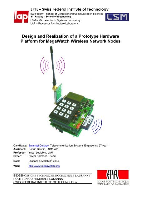
EPFL – Swiss Federal Institute <strong>of</strong> TechnologyI&C Faculty – School <strong>of</strong> Computer <strong>and</strong> Communication SciencesSTI Faculty – School <strong>of</strong> EngineeringLSM – Microelectronic Systems LaboratoryLAP – Processor Architecture Laboratory<strong>Design</strong> <strong>and</strong> <strong>Realization</strong> <strong>of</strong> a <strong>Prototype</strong> <strong>Hardware</strong><strong>Plat<strong>for</strong>m</strong> <strong>for</strong> MegaWatch Wireless Network NodesC<strong>and</strong>idate: Emanuel Corthay, Telecommunication Systems Engineering 5 th yearAssistant: Cédric Gaudin, LSM/LAPPr<strong>of</strong>essor: Yusuf Leblebici, LSMExpert: Olivier Carmona, KteamDate: Lausanne, March 8 th 2004Web:http://www.megawatch.org/______________________________________________________EIDGENÖSSICHE TECHNISCHE HOCHSCHULE LAUSANNEPOLITECNICO FEDERALE LOSANNASWISS FEDERAL INSTITUTE OF TECHNOLOGY
ProjectThe MegaWatch Wireless<strong>Plat<strong>for</strong>m</strong>TitleMaster's Thesis - Emanuel CorthayStatusVersion 1.0Keywordsmegawatch, wireless, plat<strong>for</strong>m, ad hoc, network,802.11, RF, hardware, transceiver, ARM, linux, watchExecutive SummaryThe MegaWatch project goal was to design <strong>and</strong> build a wireless network plat<strong>for</strong>m composed <strong>of</strong> 25prototype hardware units to experiment with self-organized, infrastructureless ad-hoc networks.Requirements included reconfigurable, autonomous, low power consumption, <strong>and</strong> powermeasurement capability. In the long term, it is intended that all the above functionality beintegrated in a small, watch size component.The design chosen was composed <strong>of</strong> five main blocks: two radio links, a power supply, extensionboard, <strong>and</strong> processing unit. An <strong>of</strong>f-the-shelf, XE-1202 digital radio circuit from Xemics wasselected as one radio link <strong>for</strong> low-power, short distance communications. A commercial wirelessLAN card, using the 802.11b st<strong>and</strong>ard protocol, provided a second independent monitoring radiolink. The power supply chosen was composed <strong>of</strong> three voltage regulators, a battery overdischargeprotection, <strong>and</strong> a power rectifier. The extension board supports both radio systems <strong>and</strong> contains ascreen, keyboard, buttons <strong>and</strong> LEDs to interact with the user. Two microcontrollers within theprocessor <strong>and</strong> extension board contain an ADC converter used <strong>for</strong> power measurements. The oneon the extension board also controls the LCD <strong>and</strong> keyboard <strong>of</strong> each unit. For maximum flexibility,the heart <strong>of</strong> the system is composed <strong>of</strong> an Altera Excalibur circuit, made up <strong>of</strong> an ARM9 system<strong>and</strong> a reprogrammable FPGA in a single chip.To run on the ARM9 system, the Linux operating system was selected. It was chosen <strong>for</strong> the gooddevelopment environment it provides, <strong>and</strong> the large number <strong>of</strong> free-s<strong>of</strong>tware applications <strong>and</strong>drivers available <strong>for</strong> it. The wireless LAN card, connected to the ARM processor, is accessiblefrom Linux to use the available wireless architecture as a monitoring network.A major component <strong>of</strong> this thesis was the design <strong>of</strong> a low level CSMA/CA based radio protocol <strong>for</strong>the short-range radio link. It was developed <strong>for</strong> low-data rate operations <strong>and</strong> implemented into theFPGA in VHDL. Six main functions were implemented including the transmission <strong>and</strong> reception <strong>of</strong>variable length payload frames <strong>of</strong> up 64 bytes, 2 FIFO buffers to store the payload, a CRC functionto detect erroneous transmission, as well as a hardware frame generator <strong>for</strong> ping <strong>and</strong> emergencymessage transmission. A 3-wire serial interface controller, used to program the external radiocircuit, was also part <strong>of</strong> the FPGA programming. During the FPGA design phase, importantper<strong>for</strong>mance parameters such as mode switching time <strong>and</strong> carrier detection system <strong>for</strong> the radiocircuit were identified.Fabrication <strong>of</strong> the 25 prototype two layer power supply <strong>and</strong> extension PCBs was done exclusivelyat EPFL, while the 12 layer main unit PCB was manufactured externally. A total <strong>of</strong> over 18,000components were ordered.Key future improvements include ad-hoc routing algorithms <strong>and</strong> application, power measurements<strong>and</strong> radio sub system protocol extensions. A Human-Machine-Interface will be developed usingthe keyboard <strong>and</strong> LCD to build a complete end user ad-hoc application.EPFL – Swiss Federal Institute <strong>of</strong> TechnologyCopyright © 2004 Emanuel Corthay – emanuel.corthay@a3.epfl.chPermission is granted to copy, distribute <strong>and</strong>/or modify this document under the terms <strong>of</strong> the GNUFree Documentation License, Version 1.2 or any later version published by the Free S<strong>of</strong>twareFoundation. A copy <strong>of</strong> the license is included at http://www.gnu.org/licenses/fdl.html
The MegaWatch Wireless <strong>Plat<strong>for</strong>m</strong>Master's Thesis - Emanuel Corthay1 IntroductionTable <strong>of</strong> Contents1 INTRODUCTION 62 SCOPE AND PURPOSE 83 BACKGROUND 103.1 Today’s Wireless Network Systems 103.2 The Next Generation Ad-hoc Network Topology 103.3 Possible Applications 113.4 Existing St<strong>and</strong>ards 114 PROJECT GOALS 144.1 Long Term Vision 144.2 Master’s Thesis Work 165 PRELIMINARY RESEARCH 185.1 DoCoMo’s “Wristomo” Wristwatch mobile phone 185.2 Swatch GSM phone 195.3 Swatch Syncro Beat 195.4 Micros<strong>of</strong>t SPOT watches 195.5 WiseNET (CSEM) 195.6 BTNodes 205.7 Motes – TinyOS 205.7.1 UC Berkeley Motes (MICA) 205.7.2 Telos 802.15.4 Motes 215.8 IBM Linux Watch 215.9 MICS – Mobile In<strong>for</strong>mation <strong>and</strong> Communication Systems 226 THE MEGAWATCH HARDWARE PLATFORM DESIGN 246.1 Requirements 246.2 Overview 246.3 Main Processor Board 256.3.1 Introduction 256.3.2 <strong>Design</strong> choice 266.3.3 RokEPXA 276.4 Radio Links 286.4.1 Low Power Ad-hoc Link 286.4.2 WiFi Link 306.5 MegaWatch Extension Board 316.6 Power Measurement 346.7 Power Supply Boards 367 THE PROTOCOLS 383 / 81
The MegaWatch Wireless <strong>Plat<strong>for</strong>m</strong>Master's Thesis - Emanuel Corthay1 Introduction7.1 Radio Protocol <strong>for</strong> the RF Circuit 387.1.1 Layer 1 – The Physical Layer ; Digital Modulation 397.1.2 Layer 2 – The Data Link Layer 417.1.3 Layer 3 – The Network Layer; Ad Hoc AODV 467.2 WiFi card : Wireless LAN 802.11b 467.3 Radio Circuit 3-wire Control Interface 467.4 Microcontroller Communication : I 2 C Interface 477.5 Conclusion 478 THE SOFTWARE 488.1 FPGA Radio Transceiver Core 488.1.1 Registers 498.1.2 Avalon Bus Controller 498.1.3 MAC Controller 508.1.4 Transmit Encoder 548.1.5 Receive Decoder 558.1.6 Transmitter <strong>and</strong> Receiver FIFO 568.1.7 Status Register 568.1.8 Control Register 578.1.9 CRC Generator <strong>and</strong> Decoder 588.1.10 R<strong>and</strong>om Number Generator 588.2 3-wire Control Core 588.3 Other Cores 608.4 Application S<strong>of</strong>tware 618.5 Microcontroller S<strong>of</strong>tware 618.6 Conclusion 619 THE MEGAWATCH PLATFORM FABRICATION 649.1 <strong>Design</strong> Phases 649.2 MegaWatch Extension Boards 659.3 Main Processor Board 679.4 Power Supply Board 689.5 Conclusion 6810 OPERATING SYSTEM 7011 AROUND THE PROJECT 7211.1 Project management 7211.2 Documents 7211.2.1 The MegaWatch Web Site 7211.2.2 Announcements 7211.3 Future <strong>of</strong> the Project 7211.3.1 Improvements 7211.3.2 Semester <strong>and</strong> Master projects 7312 CONCLUSION 7813 ACKNOWLEDGEMENTS 794 / 81
The MegaWatch Wireless <strong>Plat<strong>for</strong>m</strong>Master's Thesis - Emanuel Corthay1 Introduction14 ABBREVIATIONS AND DEFINITIONS 8015 REFERENCES 8216 APPENDICESA. Component Selection Lista. MegaWatch Extension Boardb. Power Supplyc. RokEPXA_BB. Boards Schematicsd. MegaWatch Extension Boarde. Power Supplyf. RokEPXA_BC. PIN listD. Current Sense Resistors Estimated valuesE. Radio Core Detailed ViewF. Xemics Radio Circuit DatasheetG. VHDL Source CodeH. Development ToolsI. Partners In<strong>for</strong>mation5 / 81
The MegaWatch Wireless <strong>Plat<strong>for</strong>m</strong>Master's Thesis - Emanuel Corthay1 Introduction1 IntroductionImagine wearing a watch that is more than just a watch. A watch that would be capable <strong>of</strong>exchanging in<strong>for</strong>mation with neighbouring watches. A watch that will locate your best friend youhave not seen in ages, <strong>and</strong> tell you he happens to be just around the corner, <strong>and</strong> send him ainvitation to join you <strong>for</strong> dinner right after lectures?This is the idea behind the MegaWatch project, a term project that spans beyond labs, faculty, <strong>and</strong>even EPFL; building a single low power chip with wireless capabilities that can go into a watch.This Master’s thesis work is but the first 6 months <strong>of</strong> this long term research project that will resultin 20 communicating prototype units, incorporating many different features to enable the researchef<strong>for</strong>ts <strong>of</strong> various EPFL laboratories. The challenge is to put together many different engineeringfields into a working prototype plat<strong>for</strong>m within a limited time <strong>and</strong> budget.Figure 1 The MegaWatch in the future every day’s life6 / 83
The MegaWatch Wireless <strong>Plat<strong>for</strong>m</strong>Master's Thesis - Emanuel Corthay1 Introduction7 / 83
The MegaWatch Wireless <strong>Plat<strong>for</strong>m</strong>Master's Thesis - Emanuel Corthay2 Scope <strong>and</strong> Purpose2 Scope <strong>and</strong> PurposeThe scope <strong>of</strong> the project is very wide. It is interdisciplinary, comprising many different engineeringfields (Electrical, Computer Science, Telecommunications …) as well as other less technicalengineering work (Project Management, Marketing, Business …). Several laboratories <strong>and</strong>different faculties at EPFL are involved, <strong>and</strong> industrial partners are interested in the project. Thepresented work is but a small piece <strong>of</strong> the whole, long term project, a snapshot <strong>of</strong> 6 months work.Thus, this document only focuses on the Master’s Thesis work done during that period <strong>of</strong> time. Itwill expose it from a high level system wide perspective. It is intended <strong>for</strong> people with engineeringskills in any discipline, <strong>of</strong>ten explaining concepts as they are used <strong>for</strong> people not familiar with them.A more in depth, thorough analysis <strong>of</strong> the different subjects involved is outside the scope <strong>of</strong> thisdocument <strong>and</strong> will be conducted later, this work being the starting point <strong>and</strong> enabler <strong>of</strong> research invarious fields.This paper is basically split into six sections:I. Introduction, background, project goalsII. Theoretical approach, design choices, protocolsIII. Practical hardware <strong>and</strong> s<strong>of</strong>tware implementationIV. Around the project, its future, conclusionV. Appendix. Practical in<strong>for</strong>mation to use the prototype units, as well as a description <strong>of</strong> thedevelopment tools can be found in this section.The document will describe the work done, explain the different design choices, encounteredproblems <strong>and</strong> challenges.The purpose <strong>of</strong> this document is to give answers to the following questions.• What is the MegaWatch project?• What are its challenges <strong>and</strong> long term research goals?• How does it work?• How can I use it <strong>for</strong> my own research?The document will continue to evolve after the Thesis report submission date. It will be taken bythe next people working on the project, in particular incorporate a rich user manual, <strong>and</strong>incorporate the work done by Cédric Gaudin, <strong>and</strong> semester project students.An abbreviations <strong>and</strong> definitions section at chapter 13 is available to help the reader throughout hisjourney into the description <strong>of</strong> this wireless communication system plat<strong>for</strong>m.8 / 83
The MegaWatch Wireless <strong>Plat<strong>for</strong>m</strong>Master's Thesis - Emanuel Corthay2 Scope <strong>and</strong> Purpose9 / 83
The MegaWatch Wireless <strong>Plat<strong>for</strong>m</strong>Master's Thesis - Emanuel Corthay3 Background3 BackgroundIn this section, today’s classical wireless network topology is presented, as well as the nextgeneration, with its possible applications. A quick overview <strong>of</strong> existing wireless st<strong>and</strong>ard ispresented.3.1 Today’s Wireless Network SystemsNowadays, almost all the wireless networks are infrastructure network. Each mobile unitcommunicates with an operator base station, the fixed infrastructure. Communications betweenmobile nodes, even if they are very close to each other, are not possible. The GSM cellular phonesystem [1] is a typical example <strong>of</strong> such an infrastructure, an operator maintained wireless network.The following picture shows how a transmission from one cell phone to another takes place. Evenwhen they are 1 meter apart from each other, the transmission always go through the base station,then the mobile operator fixed network concentrator <strong>and</strong> back to the second cell phone.MSCMobileStationBaseStationMSCMobileSwitchingCenterFigure 2 Cellular Phone Infrastructure Network3.2 The Next Generation Ad-hoc Network TopologyIn the Ad Hoc network topology, each unit can receive <strong>and</strong> transmit directly to its neighbours.Each unit then runs an ad-hoc algorithm to select the best route to reach a given destination,<strong>for</strong>warding a message from one unit to the other to the final recipient. Every node can act as arelay to <strong>for</strong>m a dense network.10 / 83
The MegaWatch Wireless <strong>Plat<strong>for</strong>m</strong>Master's Thesis - Emanuel Corthay3 BackgroundFigure 3 A self-organized, Wireless Ad Hoc NetworkToday, there are no mass market products using this technique. But a lot <strong>of</strong> research is takingplace, <strong>and</strong> it will likely become tomorrow’s network architecture <strong>of</strong> choice.It is important to keep in mind that the infrastructure will not simply disappear. Rather, the sel<strong>for</strong>ganizednetwork will be used to access the nearest fixed wireless gateway. This gateway willlink the Ad-Hoc network with a larger, long-distance communication infrastructure when necessary.More in<strong>for</strong>mation on Ad-Hoc networks can be found in [2].3.3 Possible ApplicationsIf we succeed in providing watch size, wearable, distributed wireless communication nodes, thefollowing applications could become common in the future:• Support <strong>for</strong> helping people to meet (find them, determine who’s around)• Localisation <strong>and</strong> orientation(map, directions, emergency like avalanche, …)• Text messaging <strong>and</strong> paging• Local in<strong>for</strong>mation (cafeteria menu, on-site events, weather <strong>for</strong>ecast, e-shop, roomreservation, on-site white pages, …)• Revolutionary classroom support (instant polling, paperless course slides annotations, …)• Emergency call to anybody around• Address book <strong>and</strong> planner synchronisation/sharing3.4 Existing St<strong>and</strong>ardsSeveral wireless st<strong>and</strong>ards already exist, or are being actively developed.The largest wireless network in place is the well known GSM cell phone system. It reliesexclusively on an operator architecture, composed <strong>of</strong> many base stations distributed across acountry’s territory. Phone-to-phone wireless communications are not possible.The WiFi, or wireless LAN, based on the IEEE 802.11 st<strong>and</strong>ard is a popular wireless computernetwork. Today, most laptops come with an embedded wireless card. They can communicatedirectly with each other in Ad-Hoc mode, or with a base station that anyone can buy from acomputer reseller. A lot <strong>of</strong> experiments have already been conducted based on <strong>of</strong>f-the-self 802.11components, but their functionalities are limited to the st<strong>and</strong>ard. It is thus not possible to modifythe way they interact with each other to test new transmission systems. Moreover, they aredesigned <strong>for</strong> high speed data links, going up to 54 Mbps <strong>for</strong> recent models, <strong>and</strong> are not suitable <strong>for</strong>low-power applications.Bluetooth[3] is another st<strong>and</strong>ard, dedicated to very short distances, low data ratecommunications. It is intended as a replacement <strong>for</strong> cable connexions between devices at homeor in the <strong>of</strong>fice. Its range is limited to a maximum <strong>of</strong> 10 meters, <strong>and</strong> its data rate is <strong>of</strong> the order <strong>of</strong>11 / 83
The MegaWatch Wireless <strong>Plat<strong>for</strong>m</strong>Master's Thesis - Emanuel Corthay3 Background200 Kbps. The power consumption is too high <strong>for</strong> our application. The protocol has a lot <strong>of</strong>overhead, <strong>and</strong> is not flexible enough to experiment with various Ad hoc protocols. It is <strong>for</strong> instancelimited to 8 units <strong>for</strong>ming a very small network, with one master <strong>and</strong> 7 slaves. Even though it ispossible to link together several such small networks in a so called tree squatternet network, moreadvanced topologies are not possible. For more in<strong>for</strong>mation, please consult [4].An emerging st<strong>and</strong>ard, the IEEE 802.15.4 [5] (also known as ZigBee [6]) is being activelydeveloped. It is intended specifically <strong>for</strong> low-speed (20 to 250 Kbps), low-power devices. Thespecifications are still in the draft phase, <strong>and</strong> no products were available <strong>for</strong> testing at thebeginning <strong>of</strong> this work. This is not true anymore, <strong>and</strong> as <strong>of</strong> February 2004, products compliant withthe draft version are starting to appear on the market. This st<strong>and</strong>ard should be closely monitoredin the future to see if it can be incorporated into MegaWatch as the wireless connectivity st<strong>and</strong>ardto support ad-hoc network applications.No existing solution was satisfactory to experiment <strong>and</strong> develop low-power, flexible Ad-Hocnetworks at the beginning <strong>of</strong> this work. Various testing hardware plat<strong>for</strong>ms (see section 5) havebeen developed in recent years, but do not meet the requirements set <strong>for</strong> this project in the nextsection.12 / 83
The MegaWatch Wireless <strong>Plat<strong>for</strong>m</strong>Master's Thesis - Emanuel Corthay3 Background13 / 83
The MegaWatch Wireless <strong>Plat<strong>for</strong>m</strong>Master's Thesis - Emanuel Corthay4 Project GoalsFuture Industrial Partners: CSEM, STI, Swatch- Technical Know-how- RF front-end- Market knowledge- Manufacturing <strong>and</strong> Packaging <strong>for</strong> large quantities- Costs optimization- MarketingA pole <strong>of</strong> competency has been <strong>for</strong>mally created under the name CSDA, Center <strong>for</strong> AdvancedDigital Systems. It incorporates most <strong>of</strong> the laboratories mentioned above, <strong>and</strong> some industrialpartners that are important <strong>for</strong> a lot <strong>of</strong> research <strong>and</strong> development projects involving hardware.That is because the gap between the academic <strong>and</strong> commercial perspective is important, <strong>and</strong> it is<strong>of</strong> great importance to work together to produce viable solutions to face tomorrow’s challenges.Network architecture:The envisioned MegaWatch network plat<strong>for</strong>m is a multi-tiered wireless network, composed <strong>of</strong> threelayers. In the campus environment, it can be described as follows:Layer 1:High-density network <strong>of</strong> low-cost, ultra-low-power MegaWatch intelligent terminals worn by everystudent. They communicate between themselves <strong>and</strong>/or with larger units acting as a gateway vialow-frequency data links.Layer 2:High per<strong>for</strong>mance mobile computing TermiNodes that act as computing plat<strong>for</strong>m <strong>and</strong> asintermediate jump-station (gateway) <strong>for</strong> wireless communication. Communication withMegaWatch(es) via low-frequency, with base-stations via high-frequency (WiFi 802.11b).Layer 3:Fixed wireless LAN (WLAN) base-stations operating on established st<strong>and</strong>ard 802.11b. Thisinfrastructure already exists at EPFL.What the project will bring:Figure 4 The proposed MegaWatch NetworkAs explained be<strong>for</strong>e, the project will create a pole <strong>of</strong> competency necessary to face tomorrowtechnical challenges. It will also provide a test plat<strong>for</strong>m <strong>for</strong> the following domains:- Reconfigurable <strong>Hardware</strong> to explore Ad hoc Algorithms <strong>and</strong> Protocols15 / 83
The MegaWatch Wireless <strong>Plat<strong>for</strong>m</strong>Master's Thesis - Emanuel Corthay4 Project Goals- Wireless Security Experiments- Power Management, by exploring idleness detection techniques, dynamic voltage scaling<strong>and</strong> frequency scaling <strong>and</strong> power management policies- System-on-Chip, Network-on-Chip experiments- Applications <strong>and</strong> User Interface <strong>Design</strong>.Proposed Timetable:Figure 5 gives a possible project roll-out time plan:Figure 5 MegaWatch <strong>Prototype</strong>s IterationsFor more in<strong>for</strong>mation on long term goals, please consult [7] <strong>and</strong> [8].4.2 Master’s Thesis WorkAs explained be<strong>for</strong>e, the goal <strong>of</strong> this work is to develop the first MegaWatch prototype. It is mainlya technical development project that will enable a lot <strong>of</strong> ongoing research that has been waiting ona test plat<strong>for</strong>m to go further.The original project description was as follows:The goal <strong>of</strong> the Master’s thesis work is to build a low-power demonstration plat<strong>for</strong>m <strong>for</strong> ad-hocwireless network nodes. The prototype plat<strong>for</strong>m, part <strong>of</strong> a larger scientific research ef<strong>for</strong>t, willconsist <strong>of</strong> a low-power radio front-end, an reconfigurable logic unit with embedded processor(s),memory <strong>and</strong> a human-machine interface. Each prototype board will operate autonomously with itsown on-board battery, <strong>and</strong> will be capable <strong>of</strong> communicating with similar units in its receptionrange. Each unit will be required to keep an extended dynamic list <strong>of</strong> reachable-neighbour units,<strong>and</strong> to run an ad-hoc routing algorithm to receive <strong>and</strong> transmit individual data packets. The unitwill ideally be able to send time stamped event reports in real time via a 802.11b connexionintegrated on the board as a second radio link, thus allowing <strong>for</strong> independent per<strong>for</strong>manceevaluation <strong>of</strong> hardware <strong>and</strong> s<strong>of</strong>tware components (monitoring).16 / 83
The MegaWatch Wireless <strong>Plat<strong>for</strong>m</strong>Master's Thesis - Emanuel Corthay4 Project GoalsThe RF front-end will be composed <strong>of</strong> a 433 MHz 20 kb/s data transceiver, under development atCSEM.Each unit processor will preferably run Linux so that a wide range <strong>of</strong> applications can eventually beported <strong>and</strong> implemented on this plat<strong>for</strong>m.By the end <strong>of</strong> the project, it is expected that about 20 identical units will be produced <strong>for</strong> real-timead-hoc network emulation <strong>and</strong> testing purposes.Proposed timetable:Month 1-2Month 2-3Month 4-5Month 6Discrete components prototype boards composed <strong>of</strong> the RF interface,the FPGA, micro controller <strong>and</strong> a simple I/O interfaceSelection <strong>of</strong> the components, construction <strong>of</strong> the first PCB board, debuggingFinal board design after debugging, communication protocol(radio MAC, synchronization, error correction, routing, etc.). Tests with 2+ nodesFull scale tests, demonstration, Masters' thesis reportThe first part will be mainly conducted at EPFL/LSM (1-2 months), <strong>and</strong> the second at CSEMNeuchâtel. Details regarding the internship at CSEM will be discussed at the beginning <strong>of</strong> theproject as to maximize efficiency <strong>and</strong> chances <strong>of</strong> success based on partners geographicallocalisation.In parallel to the thesis work, a reference manual will be written, <strong>and</strong> a web site constructed topublicise the project results.Updated Work Goals:The industrial partnership was cancelled shortly be<strong>for</strong>e the project started. Nonetheless, theproject did not suffer from this last minute change. Another radio circuit was selected, <strong>and</strong> thenecessary competency <strong>and</strong> material was available at EPFL.Personal goals:Some <strong>of</strong> the personal goals sought during the project include:- Work on a large scale <strong>and</strong> long term project involving team work with different partners,industrial if possible- Validate what I have learnt during my five years at EPFL by doing a hardware realizationthat involves many engineering fields- Gain greater project management <strong>and</strong> engineering skills- Continue to pursue my long term goal <strong>of</strong> building a versatile universal transceiver, projectthat was started by a semester project on s<strong>of</strong>tware defined radio17 / 83
The MegaWatch Wireless <strong>Plat<strong>for</strong>m</strong>Master's Thesis - Emanuel Corthay5 Preliminary research5 Preliminary researchThis section gives a quick overview <strong>of</strong> existing projects that are similar to the MegaWatch. It is notan exhaustive product or project list. For each <strong>of</strong> them, we explain why they are not adapted to ourapplication requirements.For each presented product, the reader is invited to consult the given reference <strong>for</strong> morein<strong>for</strong>mation.5.1 DoCoMo’s “Wristomo” Wristwatch mobile phoneThis is the first commercial wristwatch-style cell phone on themarket (March 2003). Not surprisingly, it comes from Japan, acountry where people are willing to spend a lot <strong>of</strong> money onsuch devices.It is a waterpro<strong>of</strong> watch, that opens up into a functional Personal H<strong>and</strong>yphoneSystem (PHS) h<strong>and</strong>set when buttons on either side <strong>of</strong> the watch faceare pressed.The WRISTOMO is compatible with the "PALDIO E-mail" service, whichenables users to send/receive e-mails <strong>of</strong> up to 6,000 alphanumeric charactersvia the Internet without having to register with an Internet Service Provider.The wrist phone transfers data at up to 64 kbps. The WRISTOMO can accessthe "Browserphone Content" web pages <strong>of</strong> DoCoMo's service, as well as sitesbased on a subset <strong>of</strong> HTML, designed <strong>for</strong> mobile internet services. TheWRISTOMO is also equipped <strong>for</strong> DoCoMo's "Location based Web Sites,"which provide in<strong>for</strong>mation about restaurants, weather, transportation <strong>and</strong>other content based on the user's current location.The WRISTOMO comes with an in<strong>for</strong>mation synchronization feature thatautomatically exchanges in<strong>for</strong>mation with PCs, such as the address book ordaily planner. Whenever in<strong>for</strong>mation stored in the WRISTOMO or PC is changed, the other deviceis automatically updated either via the mobile Internet or an optional cable.Specifications <strong>of</strong> WRISTOMO:Height x Width x Thickness (mm) (when unfolded <strong>for</strong> h<strong>and</strong>set use) 171.5 x 40.4 x 18.5Weight (grams) Approx. 113 (including battery)Continuous talk time (minutes) Approx. 120Continuous st<strong>and</strong>-by time (hours) Approx. 200Data transmission speed 64 kbps/ 32 kbpsBody color Dark Gray MetallicA nice product, but not applicable <strong>for</strong> the MegaWatch application because PHS is an infrastructurest<strong>and</strong>ard which is not suited <strong>for</strong> ad hoc network experiments.18 / 83
The MegaWatch Wireless <strong>Plat<strong>for</strong>m</strong>Master's Thesis - Emanuel Corthay5 Preliminary research5.2 Swatch GSM phoneDeveloped at Azulab, the Swatch group laboratory, this working watch GSMphone is only a prototype, <strong>and</strong> is not commercialized. Apparently, thegroup is not planning on launching this product at the moment <strong>for</strong> severalreasons.A nice product, but again it uses GSM which is not suited <strong>for</strong> ad hocnetwork experiments. In addition, as mentioned above, it is only at theprototype stage with no near term commercial prospects.5.3 Swatch Syncro BeatThis commercial product allows its possessor to exchange smallamounts <strong>of</strong> data between compatible watches using sounds.In<strong>for</strong>mation like business cards, alarms <strong>and</strong> melodies can betransmitted by pressing a button <strong>and</strong> maintaining the watches closeto each other. So called compatibility tests can be done, indicatinghow “compatible” the person is with its peer according to a certainnumber <strong>of</strong> criteria.In the same way, the watch can exchange data with a computerequipped with a sound card <strong>and</strong> a microphone.The wireless link is audio here, <strong>and</strong> cannot exceed a range <strong>of</strong> 1-2meters, making it unusable <strong>for</strong> our application.5.4 Micros<strong>of</strong>t SPOT watchesMicros<strong>of</strong>t's Smart Personal Objects Technology initiative aims to trans<strong>for</strong>meveryday small objects like watches, key chains <strong>and</strong> pens into intelligent,communicating devices. The watch “wrist net” project uses FM broadcast stationsto receive (only) the data modulated on a sub-carrier frequency, very similar to theEuropean Radio Data System (RDS).The first SPOT watches arrived in stores at the beginning <strong>of</strong> 2004, <strong>and</strong> <strong>of</strong>fer realtime weather <strong>and</strong> stock market in<strong>for</strong>mation, as well as paging capability. It comeswith a subscription system depending on what in<strong>for</strong>mation the user wants toreceive.This is a one-way, very low data rate wireless system that doesn’t fulfil our requirements.5.5 WiseNET (CSEM)The main objective <strong>of</strong> this research ef<strong>for</strong>t is to develop a low-power wireless ad-hoc network made<strong>of</strong> many distributed microsensors that are energetically autonomous (usually battery operated) <strong>and</strong>able to communicate amongst them <strong>and</strong> with the external world.Today, much <strong>of</strong> their ef<strong>for</strong>t is focused on developing a very low-power radio transceiver that canoperate from a single 1.5 V battery <strong>and</strong> last more than 5 years. The radio <strong>and</strong> the wireless protocol19 / 83
The MegaWatch Wireless <strong>Plat<strong>for</strong>m</strong>Master's Thesis - Emanuel Corthay5 Preliminary researchare optimized <strong>for</strong> a very low duty cycle operation (typically a few percent). The radio transceiver isintegrated in a 0.18 µm st<strong>and</strong>ard digital CMOS process.Their research ef<strong>for</strong>t is more on RF front-end level, <strong>and</strong> the whole network is composed <strong>of</strong> verysmall units. They are limited to a very small memory size <strong>and</strong> computational power, <strong>and</strong> don’thave a usable product at the moment.For more in<strong>for</strong>mation, see [9]5.6 BTNodesThe BTnode is an autonomous wireless communication <strong>and</strong> computingplat<strong>for</strong>m based on a Bluetooth radio <strong>and</strong> a microcontroller. It serves asa demonstration plat<strong>for</strong>m <strong>for</strong> research in mobile <strong>and</strong> ad hoc connectednetworks <strong>and</strong> distributed sensor networks. It has been developed atETH Zurich [10].Specifications <strong>of</strong> the system:Microcontroller: Atmel ATmega 128L (8 MHz @ 8 MIPS)Memories: 64 Kbyte RAM, 128 Kbyte FLASH ROM, 4 Kbyte EEPROMBluetooth radio module, Ericsson ROK 101 007External Interfaces (ISP, UART, SPI, I2C, GPIO, ADC,...)4 LEDsSt<strong>and</strong>ard C ProgrammingBluetooth is not a viable solution <strong>for</strong> us, due to its limitations, as explained in 3.4.5.7 Motes – TinyOSTinyOS is an event based operating environment designed <strong>for</strong> use with embedded networkedsensors. More specifically, it is designed to support the concurrency intensive operations requiredby networked sensors with minimal hardware requirements. There are many TinyOS projectstaking place throughout the world, <strong>and</strong> a couple <strong>of</strong> hardware plat<strong>for</strong>m designed specifically to runthis OS. [11] The computational power is not sufficient <strong>for</strong> the envisaged MegaWatch application.5.7.1 UC Berkeley Motes (MICA)This sensor network system is based on an ATMega 128 microcontroller running at 4 MHz. Thememory is composed <strong>of</strong> a 512 K Flash, 4K <strong>of</strong> RAM <strong>and</strong> 128K <strong>for</strong> the program. The transceiver is aRFMTR1000 working at 915 MHz <strong>and</strong> 40 Kbps using ASK <strong>and</strong> has a 1 meter range. It comes withan extension sensor board.Figure 6 UC Berkley MotesThey also have a new SPEC prototype which is only a fraction <strong>of</strong> the size <strong>of</strong> the original.20 / 83
The MegaWatch Wireless <strong>Plat<strong>for</strong>m</strong>Master's Thesis - Emanuel Corthay5 Preliminary researchThe radio range <strong>and</strong> computational power <strong>of</strong> this system is too small <strong>for</strong> our application.5.7.2 Telos 802.15.4 MotesThis is the first wireless circuit implementing the new IEEE 802.15.4 protocol. It was supposed tobe available in limited quantities at the beginning <strong>of</strong> 2004, but was not there at the beginning <strong>of</strong> theproject.More in<strong>for</strong>mation can be found at [12].Figure 7 Telos 802.15.4 Mote5.8 IBM Linux WatchAn IBM initiative to put Linux in a watch. It is not yet a commercial product, <strong>and</strong> no activity hasbeen reported on this project after 2001. The latest version includes a Bluetooth link.Figure 8 IBM Linux WatchWatch size 56mm x 48mm x 12mmWeight 44gCPU Low power 32-bit CPU (18-74 MHz)I/O device Touch panel, Roller wheelDisplay 96x120dots B/W STN LCD/VGA OLEDMemory DRAM 8MB, Flash 8MBCommunication Bluetooth (V1.0Bw/voice), IrDA (V1.2), UART (Cradle)Power Li-Polymer rechargeableOther Speaker, Mic, Buzzer, Tilt sensorCradle Charger, RS232C, AC-adapterOS Linux version 2.2, GUI X11R6Bluetooth stack IBM BlueDraker (L2CAP,SDP,RFCOMM)21 / 83
The MegaWatch Wireless <strong>Plat<strong>for</strong>m</strong>Master's Thesis - Emanuel Corthay5 Preliminary research5.9 MICS – Mobile In<strong>for</strong>mation <strong>and</strong> Communication SystemsThis is not an existing product, but an interest group on wireless ad hoc networks. TheMegaWatch team keeps close ties with NIC members, who are eager to use the MegaWatchplat<strong>for</strong>m to test their theoretical results.Please consult their website at www.terminodes.org <strong>for</strong> more in<strong>for</strong>mation.22 / 83
The MegaWatch Wireless <strong>Plat<strong>for</strong>m</strong>Master's Thesis - Emanuel Corthay5 Preliminary research23 / 83
The MegaWatch Wireless <strong>Plat<strong>for</strong>m</strong>Master's Thesis - Emanuel Corthay6 The MegaWatch <strong>Hardware</strong> <strong>Plat<strong>for</strong>m</strong> <strong>Design</strong>6 The MegaWatch <strong>Hardware</strong> <strong>Plat<strong>for</strong>m</strong> <strong>Design</strong>Because existing hardware did not meet all <strong>of</strong> our requirements, a new plat<strong>for</strong>m has beendesigned. It is described theoretically in this chapter. The associated protocol, s<strong>of</strong>tware <strong>and</strong>realization is explained later in this document.6.1 RequirementsThe main requirements as stated in 4.2 are as follow:Build 20 autonomous, small <strong>for</strong>m factor wireless network units with the following characteristics:- A low-power radio interface to experiment with ad-hoc networks- A second independent radio link <strong>for</strong> real time monitoring <strong>of</strong> the units behavior- A powerful, easy to use, flexible processing unit to implement various communicationprotocols <strong>and</strong> applications- Power management <strong>and</strong> monitoring capabilities, <strong>for</strong> the radio subsystems as well as theprocessing unit- An intuitive, simple but yet powerful Human Machine interface to interact with the user- Several extension possibilitiesThe above must be achieved all within 6 months, thus requiring reuse <strong>of</strong> as much existing or <strong>of</strong>fthe-shelfhardware as possible. Financial constraints also influenced the design choices.6.2 OverviewThe units are separated into 5 main blocks, the 2 independent radio links supported by theMegaWatch extension board, the processor unit <strong>and</strong> the power supply. The RF link is the lowpowerradio system, whereas WiFi is the Wireless LAN link.UserRFMegaWatch Extension BoardCFWiFiMilli-BUSProcessor UnitA-BUSPower Supply BoardCircuitBoardExternalcomponentBusesFigure 9 MegaWatch Unit System Overview24 / 83
The MegaWatch Wireless <strong>Plat<strong>for</strong>m</strong>Master's Thesis - Emanuel Corthay6 The MegaWatch <strong>Hardware</strong> <strong>Plat<strong>for</strong>m</strong> <strong>Design</strong>Each block is linked to the other via a bus. The two bus specifications are the result <strong>of</strong> team workamong students doing related projects at LAP. They are available on the MegaWatch website at[13] <strong>and</strong> [14].The Wireless LAN uses a st<strong>and</strong>ard Compact Flash (similar to PCMCIA) connector, <strong>and</strong> the RF isdirectly piggy-backed to the extension board.The processor unit used in this project is a revision <strong>of</strong> Cédric Gaudin’s original diploma work, theRokEPXA board. The RF <strong>and</strong> WiFi block are <strong>of</strong>f-the-shelf commercial products that we interfacedthrough the extension board to the system. The MegaWatch board has been entirely designed<strong>and</strong> built during this project. The power supply board is also an original work, but conducted jointlywith Cédric Gaudin.6.3 Main Processor Board6.3.1 IntroductionThe main board contains the heart <strong>of</strong> the system. It’s where the various data coming from theperipherals are analyzed <strong>and</strong> used according to a piece <strong>of</strong> s<strong>of</strong>tware that runs on a microprocessor.The s<strong>of</strong>tware can be st<strong>and</strong> alone or integrated within an operating system (OS). In the first case, itis compiled <strong>for</strong> the given processor or microcontroller architecture into fundamental instructionsexecuted sequentially. The developer must take care <strong>of</strong> everything. Moreover, having twodifferent applications running concurrently is not an easy task.By contrast, it can also be integrated within an OS. For more complex, integrated applications, theOS version is preferred, because a lot <strong>of</strong> features are made available to the developer throughst<strong>and</strong>ard, portable functions <strong>of</strong> the operating system.On embedded devices like the MegaWatch units, the available space, computational power <strong>and</strong>memory is a scarce resource. Thus, the OS <strong>and</strong> processor must be carefully chosen toaccommodate these special needs <strong>and</strong> use the available hardware as efficiently as possible. Atthe same time, the development must be as easy as possible <strong>for</strong> the developer.Another important thing to consider is the interface, or how to connect a given device to theprocessor. For advanced <strong>and</strong> wide-spread peripherals like memory, st<strong>and</strong>ard system bus definingthe electrical way to connect such a device to a processor exists. Examples include SDRAM, PCI,PCMCIA <strong>and</strong> CompactFlash. Most commercial processors then implement the bus directly on theprocessor through a certain number <strong>of</strong> specialized connections (referred to as PINs later in thisdocument), <strong>and</strong> include the associated controller on the chip. For less dem<strong>and</strong>ing peripherals,st<strong>and</strong>ard serial controllers <strong>for</strong> RS-232, I 2 C or SPI buses are usually integrated on most embeddedprocessors. That’s because they are very common <strong>for</strong> small peripherals like sensors, ADC <strong>and</strong>motors, or simply to communicate with a st<strong>and</strong>ard PC.This sounds like a very promising interface, but requires fairly complex peripherals with a controller<strong>for</strong> the given bus. At the same time, such a peripheral is usually composed <strong>of</strong> a monolithic, staticchip known as ASIC (Application-Specific Integrated Circuit). The advantage <strong>of</strong> these dedicatedchips is their low cost due to high volume manufacturing, <strong>and</strong> high speed, because the logic on thechip is dedicated to a certain task. On the other h<strong>and</strong>, if the features <strong>of</strong>fered do not meet therequirements <strong>for</strong> a system, there is no way to change them. That’s where an intermediate,reprogrammable solution comes into the picture. One such solution is an FPGA, or FieldProgrammable Gate Array. It not only <strong>of</strong>fers a flexible, custom interface solution, but can alsoimplement various programmable functions, as illustrated in figure 10.25 / 83
The MegaWatch Wireless <strong>Plat<strong>for</strong>m</strong>Master's Thesis - Emanuel Corthay6 The MegaWatch <strong>Hardware</strong> <strong>Plat<strong>for</strong>m</strong> <strong>Design</strong>RFCustomPeripheralCustomInterface<strong>Hardware</strong>DataProcessingFPGASt<strong>and</strong>ardBusPeripheralsProcessorMemoryS<strong>of</strong>twareConfigurationFigure 10 General System PrincipleApplicationS<strong>of</strong>twareThe FPGA is basically composed <strong>of</strong> a large number <strong>of</strong> logical cells that can implementfundamental logic functions like logical gates, flip-flop <strong>and</strong> so on. Each cell is configured accordingto a static RAM memory that is loaded at startup from a configuration file sent to the chip. Theresult is a flexible hardware logic system with a s<strong>of</strong>tware component to configure the embeddedlogic. The FPGA also has drawbacks. It is generally more expensive than an ASIC solution <strong>for</strong>large production, consumes more power (the configuration memory essentially) <strong>and</strong> runs at lowerfrequency than an ASIC version (fixed wired network). But such a system is very powerful to test adesign (prototyping) be<strong>for</strong>e mass production, or <strong>for</strong> custom, low volume solutions. The reason issimple: you can program a complete system in s<strong>of</strong>tware that you want your hardware FPGA logicgates to do, <strong>and</strong> if it does not work as expected, you can simply change the code! The advantage<strong>of</strong> the s<strong>of</strong>tware approach (its flexibility) <strong>and</strong> <strong>of</strong> the hardware approach (its fast speed <strong>for</strong> dedicatedtasks) is thus united in a single FPGA circuit.For our application, where flexibility is a requirement, an FPGA solution is ideal. The radiosubsystem can be programmed into this FPGA, changed <strong>and</strong> tested at will. Also, once a goodradio subsystem runs on the FPGA, a real hardware, gate-level circuit design can be createdautomatically from the FPGA configuration s<strong>of</strong>tware, <strong>and</strong> integrated later as part <strong>of</strong> a dedicatedASIC circuit.6.3.2 <strong>Design</strong> choiceAltera has a chip family called Excalibur with the nice property <strong>of</strong> having both an FPGA <strong>and</strong>complete ARM9 processor system in a single chip. It also has the appropriate <strong>and</strong> integrated toolsto easily combine an FPGA <strong>and</strong> ARM design into a powerful <strong>and</strong> versatile system.Moreover, a Linux distribution <strong>for</strong> the ARM processor architecture exists <strong>and</strong> is being activelydeveloped as a joint <strong>and</strong> distributed free s<strong>of</strong>tware ef<strong>for</strong>t around the globe. This last argument setthe operating system that will be used to Linux as the application development environment.The selected Altera Excalibur ARM EPXA1F484C3 [15] chip has the following characteristics:• An ARM922T processor running at 133 MHz• A SDRAM SDR <strong>and</strong> DDR memory controller (512 Mo max)• Internal 32 Ko SRAM memory• Internal 16 Ko double access SRAM memory• External memory interface <strong>of</strong> maximum 4 times 32 Mo• Interrupt controller, UART <strong>and</strong> timers• FPGA with 100’000 logical gates running at 24 MHz26 / 83
The MegaWatch Wireless <strong>Plat<strong>for</strong>m</strong>Master's Thesis - Emanuel Corthay6 The MegaWatch <strong>Hardware</strong> <strong>Plat<strong>for</strong>m</strong> <strong>Design</strong>It is very important to distinguish between the reconfigurable part <strong>of</strong> the Excalibur, <strong>and</strong> its VLSIARM part. The reconfigurable part, the FPGA, composed <strong>of</strong> hardware logic can host manydifferent systems, known as cores, according to a loaded s<strong>of</strong>tware configuration. Because itcontains both a s<strong>of</strong>tware <strong>and</strong> hardware component, it is commonly called “s<strong>of</strong>t-core” where as theVLSI part, burnt <strong>for</strong> once <strong>and</strong> <strong>for</strong> all into the chip, is called “hard-core.” These two componentsinteract with each other through a bridge, present on the chip.Building a Printed Circuit Board (PCB) to link the different hardware circuits <strong>for</strong> the Excalibur is alot <strong>of</strong> work. Fortunately, it has been successfully realized in Cédric Gaudin’s Master’s thesis workin March 2003 [16]. The card was named RokEPXA. A slightly modified version, called revision B,<strong>of</strong> Cédric’s original design was made. The main new feature is the addition <strong>of</strong> a powermeasurement device explained in 6.6.6.3.3 RokEPXAThe general architecture <strong>of</strong> the RokEPXA board is as follow:JTAGProgrammingInterfaceRS232PowerMeasurementAlteraExcaliburI 2 CA BUSPowerSupplySDRAMMemory64 MBExtensionConnectorsARMBridgeFPGAI 2 CSerial BusFlashMemory8 MBUSBConnectorFigure 11 RokEPXA rev. B OverviewMilli BUSMegaWatchExtensionThe memory controller <strong>of</strong> the Excalibur is connected to the two memories. An internal UARTpresent on the ARM part <strong>of</strong> the Excalibur provides a serial RS-232 interface. The lines dedicatedto the FPGA are connected to various connectors. Around 60 <strong>of</strong> them are connected to the Milli-Bus, allowing an extension board to be piggy-backed on top <strong>of</strong> the main board.The programming <strong>and</strong> debugging interface to the ARM <strong>and</strong> FPGA are accessible on the boardthough a dedicated connector. The same is true <strong>for</strong> the microcontroller used <strong>for</strong> the powermeasurement, as explained in Chapter 6.6.The ARM processor comes with a bus to link it with external peripherals named AHB. The ARMspecifications provide in<strong>for</strong>mation as to how to communicate on this bus. Two versions <strong>of</strong> this busare present on the Altera Excalibur chip. The first one, AHB1, is directly connected to the memory27 / 83
The MegaWatch Wireless <strong>Plat<strong>for</strong>m</strong>Master's Thesis - Emanuel Corthay6 The MegaWatch <strong>Hardware</strong> <strong>Plat<strong>for</strong>m</strong> <strong>Design</strong>controller. The ARM is the only master on the bus. The second one, AHB2, is slower <strong>and</strong> is usedto connect to the different peripherals. In particular, it integrates the two bridges to the FPGA, one<strong>for</strong> the communication from the FPGA to the ARM, <strong>and</strong> one <strong>for</strong> the communication from the ARMto the FPGA. Figure 12 illustrates the internal structure <strong>of</strong> the Excalibur.ARM922TInterruptControllerWatchdogTimerSDRAMMemoryControllerUART(Flash)EBISlaveAHB1-2BridgeMasterAHB1ConfigurationLogicMasterAHB2MasterBridgeDPRAM1x16KoSRAM2x16Ko2xPLLResetmodule2xTimerSlaveBridgeSlaveMasterFPGAFigure 12 Internal Excalibur StructureFor more in<strong>for</strong>mation, see Cédric Gaudin’s report [16]. For more in<strong>for</strong>mation on the manufacturing<strong>of</strong> the cards, see 9.3.The electrical schematic is available in the appendix, as well as the physical line schematic,realized at EPFL/ACORT by George Vaucher.6.4 Radio Links6.4.1 Low Power Ad-hoc LinkBuilding a br<strong>and</strong> new radio circuit is a huge task. While digital systems, only attempting torecognize 1 from 0, tend to accommodate signal degradations, working with analog high frequencycomponents requires careful design. A good knowledge <strong>of</strong> issues related to this very sensitivespecialized field is necessary. The critical issue is related to the electromagnetic field effect. Athigh frequencies, strong signal interferences appear in adjacent lines, creating crosstalk problems.Bad impedance matching on lines creates reflected waves, further degrading the signal. To avoidthis problem, all lines must be matched to a given impedance. Sensitivity, linked to the noise in thesystem becomes a vital point, is one <strong>of</strong> the most important per<strong>for</strong>mance parameters <strong>of</strong> an RFcircuit.28 / 83
The MegaWatch Wireless <strong>Plat<strong>for</strong>m</strong>Master's Thesis - Emanuel Corthay6 The MegaWatch <strong>Hardware</strong> <strong>Plat<strong>for</strong>m</strong> <strong>Design</strong>Even though experience is this field exists [17], it would be a Master’s thesis work in itself.Furthermore, the integration <strong>of</strong> an analog part in a single SoC solution comes later in this long termproject anyways. For all these reasons, it was decided that a commercial <strong>of</strong>f-the-shelf productwould be used <strong>for</strong> this first prototype in the <strong>for</strong>m <strong>of</strong> a mounted development kit. This approach alsominimizes the risks <strong>and</strong> speeds up the prototyping process, in order to have a first working solutionas a pro<strong>of</strong>-<strong>of</strong>-concept be<strong>for</strong>e going further in the project.Several products were considered <strong>and</strong> compared. Some <strong>of</strong> their characteristics are shown inTable 1 below. The first priority was to have a small power consumption. That includes theconsumption in transmit mode, but also in receive mode, <strong>and</strong> most importantly, in idle mode. Theraw transmission power, usually adaptable, is not the main criteria.The link frequency <strong>and</strong> speed is also <strong>of</strong> great importance. In general, when the carrier frequencyincreases, the power required to transmit increases as well, but so does the available throughput.For a given low volume traffic, if the speed is too slow, the latency time is greater, <strong>and</strong> theprobability <strong>of</strong> having two nodes transmitting at the same time, called a collision, is higher, becauseeach individual transmission lasts longer. On the other end, with a fast transmission, the radi<strong>of</strong>requency becomes free much faster after a transmission, reducing the number <strong>of</strong> requiredretransmissions because <strong>of</strong> collisions, thus reducing the overall power consumption. Several otherfactors also influence the power consumption <strong>of</strong> a radio systems, tightly linked to its per<strong>for</strong>mance.The best choice is thus not obvious. It is a question <strong>of</strong> which trade<strong>of</strong>f is the best <strong>for</strong> a givenapplication. More in<strong>for</strong>mation can be found in [18].Table 1 RF Chip ComparisonIn a previous semester project at LSM, the Nordic circuit was used. But its raw, unsynchronizedoutput makes the usage <strong>of</strong> a bit synchronizer in hardware outside the chip necessary. By contrast,both the Xemics <strong>and</strong> Chipcon circuits have a synchronized output <strong>and</strong> better per<strong>for</strong>mance, as wellas extra features like Received Signal Strength Indication (RSSI). The Chipcon chip has a betteroutput power <strong>and</strong> RSSI selection granularity, some extra power management <strong>and</strong> encodingfeatures <strong>and</strong> a faster data rate. The Xemics chip has a built-in pattern recognition system whichsends a signal when a certain synchronization bit sequence is received. The rest <strong>of</strong> the system isthus discharged <strong>of</strong> this task, saving power <strong>and</strong> programming time. It is to be noted that Xemics isa Swiss company, a spin-<strong>of</strong>f <strong>of</strong> CSEM in Neuchâtel, with which we have good contact. This is <strong>of</strong>significant importance, <strong>and</strong> can give the project team a competitive advantage when it comes tointegrating it into a single chip.It is not possible to clearly identify a winner between the Chipcon <strong>and</strong> the Xemics chip. Eventually,the Xemics development kit XM-1202 [20] available immediately was chosen. Its maincharacteristics are:• Programmable RF output power, max 15 dBm• High reception sensitivity down to –116 dBm• Low power consumption, RX 14 mA, TX 48 mA• Data rate from 4.8 to 76.8 Kbps• On chip frequency synthesizer, bit synchronization <strong>and</strong> pattern recognition29 / 83
The MegaWatch Wireless <strong>Plat<strong>for</strong>m</strong>Master's Thesis - Emanuel Corthay6 The MegaWatch <strong>Hardware</strong> <strong>Plat<strong>for</strong>m</strong> <strong>Design</strong>• Received signal strength indicator• 2-level FSK digital modulation• Maximum range around 100 meters in buildings <strong>for</strong> low speed, high power transmissionFigure 13 Xemics XM-1202 Development Kit6.4.2 WiFi LinkFor simplicity, it was obvious that a simple <strong>of</strong>f-the-shelf CompactFlash Wireless LAN card(802.11b) would be perfect to serve as a real time monitoring wireless interface. The infrastructureavailable at EPFL (WiFi base stations) is already present; Linux drivers exist; <strong>and</strong> low cost highvolume WiFi components are very easy to find.Table 2 WiFi Compact Flash Card ComparisonThe difficulty at this stage was to integrate it into the system. Not surprisingly, given the 2.4 GHzhigh frequency used, it was shown that the antenna part <strong>of</strong> the Compact Flash card must be clear<strong>of</strong> all obstacles <strong>for</strong> the link to work. In particular, if a ground plane is close to the antenna, the linkdoes not work. The antenna part <strong>of</strong> the card has been placed as to stick out <strong>of</strong> the unit to avoidthat problem.A lot <strong>of</strong> the referenced cards below were discarded <strong>for</strong> various reasons, <strong>and</strong> in the remaining lot,the Pretec was chosen simply because it had been successfully tested in the LSA2 EPFLlaboratory during the Swarm-BOT project[20] in similar conditions, <strong>and</strong> under ARM Linux.Moreover, we were able to get a good price by joining the order <strong>of</strong> WiFi cards <strong>for</strong> the two projects.30 / 83
The MegaWatch Wireless <strong>Plat<strong>for</strong>m</strong>Master's Thesis - Emanuel Corthay6 The MegaWatch <strong>Hardware</strong> <strong>Plat<strong>for</strong>m</strong> <strong>Design</strong>Figure 14 Pretec WiFi CardIts main characteristics are:• CompactFlash connector type I• 802.11b DSSS at 11, 5.5, 2 or 1 Mbps, max 14 dBm output power• Power consumption max 370 mA in transmit mode, 250 mA in receive mode <strong>and</strong> 20 mA inst<strong>and</strong>by mode• Linux drivers available <strong>for</strong> the Intersil Prism 2.5 integrated chipsetThe purpose <strong>of</strong> the WiFi card is threefold:• Provide an independent radio link <strong>for</strong> monitoring purposes• Provide a bridge possibility with the infrastructure network, thus providing a bridge to theinternet• Be available as a second radio interface <strong>for</strong> 802.11b ad hoc applications <strong>and</strong> testing6.5 MegaWatch Extension BoardThe extension card supports three major functions <strong>of</strong> the system. It must provide a practicalinterface to plug the two radio link modules, provide an easy-to-use Human-Machine-Interface, <strong>and</strong>integrate a power measurement circuit.The Figure 15 shows the general structure <strong>of</strong> the board. Each part is then discussed separately togive a good underst<strong>and</strong>ing <strong>of</strong> the design choices.31 / 83
The MegaWatch Wireless <strong>Plat<strong>for</strong>m</strong>Master's Thesis - Emanuel Corthay6 The MegaWatch <strong>Hardware</strong> <strong>Plat<strong>for</strong>m</strong> <strong>Design</strong>RFButtonsLEDsLCD96 x 40Keyboard4 x 3AddressSelectorBuzzerMilli-BUSPowerSupplyCFButtonsLEDsADCuCVoltageReferenceI 2 Cserial busFPGAARMCircuitBoardExternalcomponentWiFiOnboardComponentFigure 15 MegaWatch Extension Board OverviewThe Compact Flash interface (CF) [21] is straight <strong>for</strong>ward, <strong>and</strong> is composed <strong>of</strong> a Compact Flashconnector placed under the extension board, at the right position to allow the antenna part <strong>of</strong> thecard to stick out <strong>of</strong> the unit.The RF link extension kit comes with a st<strong>and</strong>ard 20 male poles. A female version was simplyintegrated on one side <strong>of</strong> the extension board, providing the necessary power <strong>and</strong> signal lines tothe FPGA.For the Human-Machine-Interface, a 96 by 40 dot graphic LCD from Batron[22] was chosen. Itsmain advantage, aside from its graphical capabilities, is the fact that it comes with an integrated I 2 Cserial bus controller. This means that only two wires (aside from the power lines) need to beconnected to the device, <strong>and</strong> that these two wires are shared among several devices, thusreducing the overall required number <strong>of</strong> lines.The I 2 C is also used by a Cygnal 8051 F311 microcontroller[23] to transmit the currentmeasurement to the rest <strong>of</strong> the system, as explained in 6.6.This microcontroller is also used to detect the key pressed on the relatively small 4 by 3 keynumerical keyboard, similar to those <strong>of</strong> a telephone integrated on the board. Six <strong>of</strong> the buttons arealso directly linked to the microcontroller, as well as 4 LEDs. The big advantage <strong>of</strong> this choice isthat these components are independent <strong>of</strong> the FPGA, managed locally directly by thismicrocontroller. An other big advantage is that events that need to be sent to the FPGA or theprocessor, such as key pressed, can be multiplexed on the I 2 C bus, which in turns is connected tothe rest <strong>of</strong> the system through the FPGA. The result is a reduction <strong>of</strong> used FPGA lines <strong>for</strong> theLEDs, buttons <strong>and</strong> keyboard.32 / 83
The MegaWatch Wireless <strong>Plat<strong>for</strong>m</strong>Master's Thesis - Emanuel Corthay6 The MegaWatch <strong>Hardware</strong> <strong>Plat<strong>for</strong>m</strong> <strong>Design</strong>In the future, the user will be able to type a message on the keyboard in an SMS like fashion.Also, a system <strong>of</strong> menus on the LCD can be managed directly from the microcontroller, with theappropriate s<strong>of</strong>tware (see 11.3.2).It was nonetheless decided to dedicate 7 special LEDs <strong>and</strong> 2 buttons <strong>for</strong> the RF operations. Theyare directly linked, along with two hexadecimal selectors used <strong>for</strong> the RF unit address, to theFPGA, <strong>and</strong> thus are totally independent <strong>of</strong> the microcontroller. This choice was motivated by thefollowing reasons:The radio management system will be implemented in the FPGA. In order to simplify thedevelopment <strong>of</strong> such a system, LED are extremely useful, especially in the debugging phase, asthey give a visual indication <strong>of</strong> what is going on inside the component. Additionally, the twobuttons allow the radio subsystem to be tested independently <strong>of</strong> the processor <strong>and</strong> per<strong>for</strong>m certainactions when they are pressed. Each button possesses an associated LED close to it, also linkedto the FPGA.The idea is to use one button as a ping button, <strong>and</strong> the other as an emergency button.The ping button will trigger the emission <strong>of</strong> a ping frame. Every unit that correctly received theframe will trigger the flashing <strong>of</strong> its ping LED (green), providing a visual indication <strong>of</strong> the nodes thatare within radio range <strong>of</strong> each other.The emergency button will send an emergency type frame. Each unit correctly receiving this framewill not only trigger the flashing <strong>of</strong> its emergency LED (red), but also relay the emergencyin<strong>for</strong>mation farther. Thus, every node reachable either directly or by using other units as a relaywill receive this in<strong>for</strong>mation <strong>and</strong> blinks its emergency LED, providing a visual indication <strong>of</strong> thewhole network connectivity.The user must be able to see what the radio subsystem is doing, in particular when it istransmitting <strong>and</strong> receiving. A dedicated LED <strong>for</strong> each function has been included on the extensionboard. One red LED to indicate the transmission, <strong>and</strong> one green <strong>for</strong> the reception. Additionally, 5other, more general purpose LEDs are present on the board. One has been used to indicate whenthe radio system is busy, one to indicate when the receive buffer has data <strong>for</strong> the processor, <strong>and</strong>one to indicate that data to be transmitted is stored in the FPGA <strong>and</strong> will be transmittedmomentarily. The two last LEDs do not have a particular function at the moment.The final physical layout showing the position <strong>of</strong> the various components mentioned above isillustrated in Figure 16. Pictures <strong>of</strong> the real final board are available in 9.2.33 / 83
The MegaWatch Wireless <strong>Plat<strong>for</strong>m</strong>Master's Thesis - Emanuel Corthay6 The MegaWatch <strong>Hardware</strong> <strong>Plat<strong>for</strong>m</strong> <strong>Design</strong>TrimmerBoard 7.8 x 10.5mmMilli-BUS BLED RF: busy, TX, RX at top leftRX_buf <strong>and</strong> TX_buf at top rightThen LED misc0 <strong>and</strong> 1LCD 96*40OKPing button <strong>and</strong> LEDESCRFLED uCbuzhexWiFiAntHexadecimalAddressSelectoruCKeyboard802.11b :4.3 * 4.3 under the boardhexMilli-BUS AEmergency button <strong>and</strong> LEDCompact Flash connectorunderneathFigure 16 MegaWatch Extension LayoutThe electrical schematic is available in the appendix, as well as the physical line schematic,realized at ACORT by George Vaucher.6.6 Power MeasurementMeasuring the power consumption <strong>of</strong> the various parts <strong>of</strong> the system is required, in order toevaluate the per<strong>for</strong>mances <strong>of</strong> various designs both in hardware <strong>and</strong> s<strong>of</strong>tware. The simplest way todo this is by measuring the current that flows through an element. We assume we know thesupplied voltage to that element; that should not change too much in time. One can then calculatethe consumed power by doing a simple multiplication.In order to measure the current, an Analog to Digital Converter is needed. It converts an analogvalue into a digital binary number used by the processor to estimate the current value in mA. Asolution with an ADC coupled with an integrated I 2 C bus interface was sought, but no satisfactoryoption was found. Eventually, Cédric Gaudin came up with a microprocessor system fromCygnal, a System-on-chip that integrates an ADC, a microcontroller with Flash <strong>and</strong> RAMmemory, <strong>and</strong> plenty <strong>of</strong> input output PINs in a very small size package. The price was additionallyalso very competitive compared to other st<strong>and</strong>-alone ADC solutions.The main characteristics <strong>of</strong> this C 8051 F 311 [25] microcontroller are:• Real 10 bit ADC, with up to 200 Ksps sampling rate• 25 MHz 8051 microprocessor with 1 KB internal data RAM <strong>and</strong> 16 KB <strong>of</strong> flash memory• 25 I/O ports, within which 17 can be used as an input <strong>for</strong> the ADC.34 / 83
The MegaWatch Wireless <strong>Plat<strong>for</strong>m</strong>Master's Thesis - Emanuel Corthay6 The MegaWatch <strong>Hardware</strong> <strong>Plat<strong>for</strong>m</strong> <strong>Design</strong>The general current measurement principle is shown in the figure below.RFI loadMAX4772Current SenseAmplifierLow PassFilterCygnalC8051F311microcontrollerSmall ValueSensing Resistor20xADC10 bituCI 2 CserialBUSMAX6033VoltageReference3.000 VoltFigure 17 Current Measurement CircuitA small value resistor is inserted in series into the circuit that is to be measured. It is veryimportant that the value <strong>of</strong> the resistor is small enough as to not disturb the circuit, typically lessthan an ohm. The drawback <strong>of</strong> this method is the voltage drop that exists on the resistor, <strong>and</strong> thesize <strong>of</strong> this resistor, that must be big enough to avoid heat dissipation problems.The higher the current that flows through the circuit (<strong>and</strong> thus through the resistor), the higher thevoltage potential drop on this resistor (Ohms law). This small voltage is then amplified by adedicated Maxim circuit.The output <strong>of</strong> that circuit then goes through a low pass filter, composed <strong>of</strong> a capacitor <strong>and</strong> resistorwhose value can be adjusted. This filter suppresses high frequency current changes. The result isan averaged voltage output that reflects the power consumption <strong>of</strong> the load. It ensures that <strong>for</strong> agiven ADC sampling frequency, some transitory current peaks do not affect the measurements.The result is a reading that accurately reflects the power consumption.Of course, the right measuring resistor must be carefully chosen, depending on the load. In orderto use the ADC at its maximum resolution, the maximum current measurement must correspond tothe full scale value <strong>of</strong> the converter.On the extension board, this maximum value is given by the external 3.000 voltage reference. Thecurrent sense amplifier has a gain <strong>of</strong> 20, thus, the maximum voltage on the sensing resistor mustbe 150 mV, small enough not to disturb the monitored circuit.We know that at any given time, the voltage on the resistor must not exceed 150 mV. If we knowthe maximum current that will flow through the resistor at any given time, it is then trivial todetermine the ohm value <strong>of</strong> the current sense resistor.This maximum value was estimated by practical measurements taken on the real Xemics chip <strong>for</strong>the RF part, <strong>and</strong> based solely on the datasheet specifications <strong>for</strong> the wireless LAN card, which wasnot yet available at the development time <strong>for</strong> testing.35 / 83
The MegaWatch Wireless <strong>Plat<strong>for</strong>m</strong>Master's Thesis - Emanuel Corthay6 The MegaWatch <strong>Hardware</strong> <strong>Plat<strong>for</strong>m</strong> <strong>Design</strong>On the RokEPXA main board, a second microcontroller, similar to the one available on theextension board but smaller in size <strong>and</strong> number <strong>of</strong> PINs, was used. It is a C 8051 F330. Thepower consumption <strong>of</strong> the FPGA, ARM processor <strong>and</strong> memory is achieved through monitoring <strong>of</strong>the different voltages; 1.25, 1.8, 2.5, <strong>and</strong> 3.3 volts respectively. The only difference is the gain <strong>of</strong>the current sense amplifier, as depicted on the figure below.uCADC100 x50 x50 x20 x20 xI 1.25 VI 1.8 VI 2.5 VI 3.3 VI 5.0 VFigure 18 Current Measurement on the Processor BoardIt was decided to use a second separate microcontroller on the main board, <strong>for</strong> two reasons. Thefirst reason it because it makes the measurement on the main board units possible even withoutthe extension board. The second reason, more important, is that it is very difficult to measureanalog voltages values far from where they originate, because a long signal line will cause thesignal to deteriorate quickly due to losses, noise <strong>and</strong> interference problems.For the main board, each supplied voltage was monitored during various phases <strong>of</strong> the boardactivity to determine this maximum current approximately, thus determining the current senseresistor value.More thorough measurements to determine precisely these resistors as well as the low pass filterparameters will be conducted in the future (see 11.3). At the moment, only the raw currentmeasurement value can be read <strong>and</strong> printed on the LCD in order to validate the approach.A test with an oscilloscope also shows that the voltage measured at the output <strong>of</strong> the current senseamplifier is linearly dependant on the circuit current, measured by means <strong>of</strong> a non-intrusive, currentsense probe.6.7 Power Supply BoardsOriginally, the RokEPXA boards were using Adrian Spycher’s semester project power supplyboards. These boards, called SabusAlim [25], were originally designed to supply the variousvoltages required by the RokEPXA boards, the Armonie Xscale 250 boards [26], as well as thecyclope robot. This was achieved through the design <strong>of</strong> a common power supply bus systemcalled A-BUS [14] defining physical <strong>and</strong> logical connections <strong>for</strong> the various tensions as well asconnection to the robot circuit.This 4 layer power supply design comprises not only the power regulators <strong>for</strong> the various voltagesneeded, but also an ADC <strong>for</strong> the physical sensors, 2 motors drivers <strong>and</strong> a battery charger. Theheart <strong>of</strong> the system is a PsoC from Cypress Microsystems, communicating with the main boardsthrough a SPI or I 2 C serial bus.After careful consideration, it was decided that a completely new design was advantageous. Themain reason was that these boards had features that we did not need <strong>for</strong> our application, whichwould increase cost <strong>and</strong> manufacturing time. The second reason was that we found the boardsnot mature enough, suffering from small hardware <strong>and</strong> s<strong>of</strong>tware problems. Finally, the maincomponent <strong>of</strong> the original design was no longer available on the market within a reasonable time tocomplete the project.36 / 83
The MegaWatch Wireless <strong>Plat<strong>for</strong>m</strong>Master's Thesis - Emanuel Corthay6 The MegaWatch <strong>Hardware</strong> <strong>Plat<strong>for</strong>m</strong> <strong>Design</strong>The design <strong>of</strong> these new boards was jointly conducted by Cédric Gaudin <strong>and</strong> myself. It wasoptimized <strong>for</strong> development time, manufacturing costs <strong>and</strong> reliability by making it as simple aspossible. It has only two layers, which means it can be done 100% internally at EPFL, <strong>and</strong> iscomposed <strong>of</strong> components that were available within a reasonable time to finish the project.Input6-15 VBattery 1Battery 2RectifierBypassFuse2AOverdischargeProtectionDS2720Power <strong>of</strong>f switch5VRegulatorMAX1649CSAConfigurationJumpers5VTripleRegulatorMAX1702BeGXRegulatorMAX1842EEEA-Bus5V3.3V2.5V1.25V1.8VFigure 19 Power Supply BoardA set <strong>of</strong> jumpers allow the user to select different voltages to send to the external peripherals. Thisfeature has been kept <strong>for</strong> compatibility reasons, so that the new version <strong>of</strong> the power supply canalso be used with other boards, like the Xscale250. The following set <strong>of</strong> voltages can be produced:First regulator:• 5 V, max 2.5 A (including other regulators)Triple regulator:• 3.3 Volt, max 1 A• Variable voltage between 0 <strong>and</strong> 5 V, 1.25 Volt selected, max 400 mA• 3.3, 2.5 or 1.8 V, 2.5 Volts selected, max 800 mALast regulator:• 1.5 V, 1.8 V, 2.5 V or variable between 1.1 <strong>and</strong> 5 V, 1.8 Volt selected, max 2 A37 / 83
The MegaWatch Wireless <strong>Plat<strong>for</strong>m</strong>Master's Thesis - Emanuel Corthay7 The Protocols7 The ProtocolsBe<strong>for</strong>e going into the details <strong>of</strong> the radio controller, or RF core, the choice <strong>of</strong> the communicationprotocols are exposed in this section.A protocol defines how different hardware communicates between each other, or more remotelythrough cables or radio links. It describes a common language <strong>and</strong> electrical interface used toenable interaction between hardware components.To make the definition <strong>of</strong> a communication protocol simpler, a st<strong>and</strong>ardized layer representationexists. The OSI, or Open System Interconnection, model defines a networking framework <strong>for</strong>implementing protocols in seven layers. Control is passed from one layer to the next, starting atthe application layer in one station or block, proceeding to the bottom layer, over the channel orline to the next station <strong>and</strong> back up the hierarchy.7.1 Radio Protocol <strong>for</strong> the RF CircuitIn the MegaWatch low-power radio link, the different tasks <strong>of</strong> the radio links done in the differentOSI levels, are done at different locations. Tasks that are redundant <strong>and</strong> require real timeprocessing, typically at the low physical level, are done purely in the hardware part. Tasks thatrequire more complex computation <strong>and</strong> memory, like routing decisions, are typically done ins<strong>of</strong>tware, i.e. in the processor. The following hardware <strong>and</strong> s<strong>of</strong>tware partitioning appeared to bethe most natural one, <strong>and</strong> has been applied to the low-power RF link <strong>of</strong> the MegaWatch plat<strong>for</strong>m:Layer 4 to 7To the applicationLayer 3NetworkLayer 2Data LinkLayer 1PhysicalLLCMACProvides transparent transfer <strong>of</strong> data between endsystems <strong>for</strong> end-user applicationDefines communication partners <strong>and</strong> extrarequirements like authenticationProvides packet switching, <strong>for</strong>warding, routing <strong>and</strong>sequencing, as well as addressing <strong>and</strong> errorh<strong>and</strong>lingProvides frame synchronization <strong>and</strong> errordetection <strong>and</strong> define the common rules tocommunicateMedia Access Control ; Gain access to thetransmission mediumDefines the physical connection between devices;Converts analog voltage or radio signals into a bitstreamDone in theRF chipDone in theFPGADone in theprocessorFigure 20 How <strong>and</strong> where the OSI representation is applied in the MegaWatch Units38 / 83
The MegaWatch Wireless <strong>Plat<strong>for</strong>m</strong>Master's Thesis - Emanuel Corthay7 The Protocols7.1.1 Layer 1 – The Physical Layer ; Digital ModulationPhysical signals are by nature analog signals <strong>of</strong> various levels. At some point, just about anydigital interface is reduced to a physical binary <strong>for</strong>mat, defining a common representation <strong>of</strong> a 1<strong>and</strong> a 0 in the analog world.In the wireless world, this is achieved through digital modulation <strong>and</strong> demodulation. It is similar tothe way a computer modem works, but using a much higher frequency as the carrier, one that cantravel through the air. In our case, the carrier is in the 868-870 MHz ISM (Industrial Scientific <strong>and</strong>Medical) frequency b<strong>and</strong>. No license is required to transmit in this b<strong>and</strong>, as long as the outputpower doesn’t exceed a certain level.It is outside the scope <strong>of</strong> this document to fully explain how the radio circuit works, but thefundamental principle is nonetheless explained below. Interested readers are encouraged toconsult [27] <strong>and</strong> [28] <strong>for</strong> more in<strong>for</strong>mation.The digital modulation used is FSK or Frequency Shift Keying. The transmitter transmits a certainfrequency to send a ‘1’ <strong>and</strong> an other one to send a ‘0’:‘0’f 0‘1’Frequencyf 0- ∆fFrequencydeviation2 x ∆ff 0+ ∆fMHzFigure 21 FSK Digital Modulation Examplef 0= 869 MHz∆f = 100 KHz‘1’ = 868.900 MHz‘0’ = 869.100 MHzAt the receiver end, the demodulation is done, <strong>and</strong> a logical 1 is output when the frequencycorresponding to ‘1’ is received. Alternatively, a logical 0 is output when the frequency <strong>for</strong> a ‘0’ isdetected. In a st<strong>and</strong>ard digital (LVTTL) system, the logical ‘1’ corresponds to 2.4 to 3.3 Volt <strong>and</strong>the logical ‘0’ to a voltage between 0 <strong>and</strong> 0.8 Volt in our system.Now, the real, analog world is not perfect. Noise on the transmission channel <strong>and</strong> other physicallimits makes the discrimination between a ‘0’ <strong>and</strong> a ‘1’ difficult. This is particularly true when thetransmitter switches from one symbol (0) to another (1) <strong>and</strong> does not immediately report thischange at the receiving end. There is a transitory period while the signal is changing. During thattime, it is not possible to determine whether a ‘1’ or a ‘0’ is transmitted; the signal is not stable.That is why it is <strong>of</strong> great importance to determine when the incoming signal is valid or not.To uniquely identify when the signal is valid, known as the sampling instant, it is accompanied by aclock signal. This clock, provided by the radio receiver circuit, is then used by the system todetermine when the signal should be evaluated (sampled). It is usually at the rising edge <strong>of</strong> theclock (passing from 0 to 1), indicated by an arrow in the figure below.39 / 83
The MegaWatch Wireless <strong>Plat<strong>for</strong>m</strong>Master's Thesis - Emanuel Corthay7 The ProtocolsDataSignalClockSignalTimeReceivedData StreamSamplingInstant1 1 0 1 0DetectedFrequency‘1’ Level‘0’ LevelDetectedFrequencyChip outputUnstableSignalStableSignalFigure 22 Binary Data & Recovered Clock SignalBetween two sampling times, the signal may change; going from one to zero, zero to one, orstaying unchanged indicating a repetition <strong>of</strong> the bit. The further away from the sampling instant weare, the more unstable the signal is.Unlike typical digital circuits, in which there is a data signal <strong>and</strong> a clock signal transmittedseparately, in this radio link the clock signal is not transmitted over-the-air. It must be reconstituted(i.e. recovered) by the receiver circuitry using the incoming analog signal as a base. This processis called clock recovery[] <strong>and</strong> is done in the Xemics radio circuit.In order <strong>for</strong> this synchronization process to work, the same transmission speed must be used bythe receiver <strong>and</strong> the transmitter, <strong>and</strong> must be programmed in the radio chip upon initialization.Also, in order to have a valid recovered clock at the receiver when the actual transmission bitsequence arrives, some initialization bit sequence is sent prior to the real data transmission. Thissequence is composed <strong>of</strong> 0 <strong>and</strong> 1 sent alternatively <strong>and</strong> is referred to as the preamble. It does notcontain any in<strong>for</strong>mation, but is used merely to synchronize the receiver clock with its transmitter’sequivalent.The transmission structure is explained in details in section 7.1.2.Bit synchronizer:For each incoming bit, the chip makes the best possible decision on whether the incoming signalwas a 0 or a 1. It then outputs <strong>and</strong> maintains the corresponding voltage level to rest <strong>of</strong> the systemduring an entire clock cycle. This is to ensure that the signal is stable at the sampling time, even ifthe incoming signal varies in time.Pattern Recognition Function:When no signal is present at the receiver, the ambient noise still causes the receiver to outputones <strong>and</strong> zeros with a recovered clock, but this bit stream is totally r<strong>and</strong>om. In order to detect thebeginning <strong>of</strong> a transmission from the noise, the pattern recognition function is used.The RF circuit comes with a pattern recognition module. This is a very useful feature when two ormore RF circuits are trying to establish communication. When the pattern bit sequence that weprogrammed at initialization time is detected by one <strong>of</strong> the receiver RF circuits, it sends a signal tothe rest <strong>of</strong> the system indicating that the incoming bit stream is a transmission (rather than noise)from another node.This special pattern identifying the beginning <strong>of</strong> a data frame is referred to as the Starting FrameDelimiter or SFD <strong>and</strong> is the same <strong>for</strong> all <strong>of</strong> the units.Transmission speed:40 / 83
The MegaWatch Wireless <strong>Plat<strong>for</strong>m</strong>Master's Thesis - Emanuel Corthay7 The ProtocolsThe chip supports several transmission speeds among them, 4.8, 9.6, 19.2, 38.4, <strong>and</strong> 76.8 Kbps.The speed must be programmed into the radio chip upon initialization. A speed <strong>of</strong> 38.4 Kbps hasbeen chosen <strong>for</strong> all tests related to this report. This conservative decision was taken so as toreduce transmission errors. In future work, experiments with the maximum speed will <strong>of</strong> course beconducted.The bit synchronizer <strong>and</strong> pattern recognition are functions that are integrated in the RF chip inhardware (VLSI). The signal bit stream with the recovered clock <strong>and</strong> the pattern line is then sent tothe FPGA <strong>for</strong> further processing.One last very important point to emphasize is that we are operating on a single frequency. Thismeans that we cannot transmit <strong>and</strong> receive at the same time. This type <strong>of</strong> mode <strong>of</strong> operation isknown as simplex mode.7.1.2 Layer 2 – The Data Link LayerAt this layer <strong>of</strong> the protocol, the data <strong>for</strong>mat <strong>of</strong> a basic transmission unit is defined. Because thesame radio frequency is shared among all units, a multiple access technique is put in place toarbiter the access to this shared medium.Transmission frame structure:We refer to a complete, basic transmission unit that as a frame. A frame starts after the preamble<strong>and</strong> the Starting Frame Delimiter (SFD) has been sent. It is composed <strong>of</strong> a header that containsthe source <strong>and</strong> destination address as well as other in<strong>for</strong>mation, <strong>and</strong> a payload. The end <strong>of</strong> thetransmission is made known to the receiver through the length field present in the header.The frame transmission <strong>for</strong>mat is depicted in the figure below:24 16 6 38 to (38 + 512) 16 bitsPreamble SFD Length MAC Payload CRCHeader 38 bits6 6 6 6 3 1 1 8 1 VariableTA RA SA DA Type Ack Res Seq# More Payload0 to 64 BytesVariable length PayloadFigure 23 Frame FormatPreamble: 24 alternating 0 <strong>and</strong> 1 bits to synchronize the clock <strong>of</strong> the receiving endSFD:Length:16 bits used as a Start Frame Delimiter. Used to discriminate between the r<strong>and</strong>om bitstream from the receiver when no valid signal is present from the beginning <strong>of</strong> a datapacket. When this sequence is received, the PFGA starts storing the data received tosee if it is a valid packet.Indicate the size <strong>of</strong> the payload in Bytes. Set to zero if the packet only has a header.41 / 83
The MegaWatch Wireless <strong>Plat<strong>for</strong>m</strong>Master's Thesis - Emanuel Corthay7 The ProtocolsCRC:TA:RA:SA:DA:Type:A 16 bit Cycle Redundancy Check checksum. This is used as a simple error detectionmechanism. If the computed CRC <strong>for</strong> a received frame does not correspond to theCRC sent along with the frame, it is discarded.Transmitter address. Address <strong>of</strong> the unit currently transmitting the frame.Receiver Address. Address <strong>of</strong> the unit to which the transmitted frame is aimed at.111111 is the broadcast address.Source Address. Address <strong>of</strong> the frame originator.Final Destination Address. 111111 is the broadcast address.The type <strong>of</strong> the packet, according to the following table:ACK flag:Reserved flag:000 High Priority data Frame *001 Normal Data Frame010 HELLO Frame *011 Reserved <strong>for</strong> Route Discovery Frame *100 Ping Frame101 RTS/CTS Frame *110 Emergency Frame111 Reserved* not implemented, see 11.3Table 3 Packet TypesIndicates whether the frame is an acknowledgement frame. It has beenseparated from the type field to allow acknowledgements to be included inreply frames.Flag reserved <strong>for</strong> future use.Sequence number: Used to uniquely identify a frame in conjunction with the source <strong>and</strong>destination address.More flag:Payload:Set to 1 to indicate that more frames are coming.The in<strong>for</strong>mation to be transmitted to the application.At the moment, there is no source coding techniques used. The bits are transmitted in a rowthrough the medium. It is specified that in order <strong>for</strong> the synchronization between the receiver <strong>and</strong>transmitter to hold, there must be at least one transition from 0 to 1 or from 1 to 0 per 8 transmittedbits. Transmitting more than 8 zeros or ones in a row may result in transmission errors. Thus,some future improvements should include coding to suppress this problem, as well as to improveper<strong>for</strong>mance <strong>and</strong> reliability. See 11.3 <strong>for</strong> more details on future improvements.Starting Frame Delimiter Length Choice:We assume that the incoming detected bit is a r<strong>and</strong>om variable. It has value 1 <strong>and</strong> 0 withprobability ½. With a SFD <strong>of</strong> r bits, the probability to detect this sequence in a r<strong>and</strong>om bit streamis:Probability <strong>of</strong> detection <strong>of</strong> a r bits SFD <strong>for</strong> r r<strong>and</strong>om bits:1 1P (SFD detected | r=16 r<strong>and</strong>om bits) = 2 r =16 = ≈ 15 · 1021 -665536For a binomial r<strong>and</strong>om variable, the probability <strong>of</strong> detection <strong>for</strong> n trials is given by:42 / 83
The MegaWatch Wireless <strong>Plat<strong>for</strong>m</strong>Master's Thesis - Emanuel Corthay7 The ProtocolsP (k detections in n trials) =Cnkpk( 1− p)n−kAt 38.4 Kbps, we have 38400 bits coming every second, or a bit every 26 µS. For a firstapproximation, we assume that <strong>for</strong> each incoming bit, we test <strong>for</strong> the SFD independently <strong>of</strong> theprevious bits.Thus, the average time, or mean value <strong>of</strong> detection per second is given by:1E (k) = average number <strong>of</strong> detection <strong>for</strong> 38’400-16 trials = p · n =16 · 38’384 ≈ 0.582Thus, the average number <strong>of</strong> detections in 1 second is 0.58, <strong>and</strong> the average time between twoerroneous detection is 1.7 seconds. This figure is verified in practice, the receive LED blinks atthat average speed. Fortunately, the CRC check discards most <strong>of</strong> these erroneous start <strong>of</strong>transmission detections, but in the future, a SFD <strong>of</strong> 24 or even 32 bits (maximum number <strong>for</strong> theon-chip pattern recognition function) should be used.Multiple Access TechniqueBecause several units compete to access the shared wireless medium, a multiple accesstechnique has to be used. CSMA/CA, Carrier Sense Multiple Access with Collision Avoidance, isused in our case <strong>and</strong> is the same access technique used in the wireless 802.11 st<strong>and</strong>ard.CSMA/CA:The basic principle is to sense the channel be<strong>for</strong>e transmitting, <strong>and</strong> to never transmit if it is in use.But even if a node senses the medium as idle <strong>and</strong> starts transmitting, another node may do thesame at the same time. Such an event is called a collision, resulting in the loss <strong>of</strong> one or bothframes transmitted because they become jammed. Due to the difficulty in wirelesscommunications to detect such a collision, mechanisms have to be implemented to avoid them,<strong>and</strong> to recover from them when they happen by retransmitting the in<strong>for</strong>mation.The first thing to do is to implement an acknowledgement mechanism. The receiver sends a shortacknowledgement frame to the sender, <strong>and</strong> if the sender does not receive it, it assumes that therewas a problem with the transmission. Problems not only result from collisions, but also fromperturbations <strong>of</strong> the radio link due to fading, noise, multipath, etc.Imagine the scenario depicted in Figure 24. Two nodes C <strong>and</strong> D want to transmit a frame, but themedium is busy because a third node A is transmitting.43 / 83
The MegaWatch Wireless <strong>Plat<strong>for</strong>m</strong>Master's Thesis - Emanuel Corthay7 The ProtocolsAFrom A to BBBlockedBlockedCDFigure 24 Transmitting Scenario ; C <strong>and</strong> D blocked (medium busy)Without a collision avoidance mechanism, as soon as the medium is free, node C <strong>and</strong> D will starttransmitting. Even worse, node B will start transmitting an acknowledgement (Ack) frame too,resulting in a massive collision depicted on Figure 25.AAckB to ABCollisionC to BCollision <strong>and</strong>Receiver <strong>of</strong>fCD to CDFigure 25 The medium becomes free, multiple transmissions; collisionsTo avoid this collision problem, a collision avoidance mechanism is used. Different types <strong>of</strong> frameshave different priorities. These priorities are reflected in the Inter Frame Spaces (IFS.Upon medium liberation, the transmitters will wait <strong>for</strong> the medium to be sensed as idle <strong>for</strong> a givenIFS according to the frame type.Acknowledgement packets should always have the highest priority to complete a transmission assoon as possible. Thus, the acknowledgement frame has a Short IFS (SIFS). When the mediumhas been sensed as idle <strong>for</strong> SIFS, the acknowledgement frame will be transmitted.For normal frames a longer IFS or DIFS (Distributed Coordination Function IFS) is used. When themedium has been sensed as idle <strong>for</strong> a time larger than DIFS, the normal frame can be sent.44 / 83
The MegaWatch Wireless <strong>Plat<strong>for</strong>m</strong>Master's Thesis - Emanuel Corthay7 The ProtocolsThis again will lead to collisions when two nodes want to transmit a normal frame. Thus, ar<strong>and</strong>omized back-<strong>of</strong>f time will be selected independently on each node <strong>and</strong> added to the DIFS timebe<strong>for</strong>e transmission. That method ensures that the probability <strong>of</strong> collision is now a r<strong>and</strong>omvariable.The r<strong>and</strong>omized back-<strong>of</strong>f time is a multiple <strong>of</strong> the slot time. The slot time is essentially themaximum time it takes to detect that another station is transmitting.DIFSDIFSSIFSMedium BusyAccess DelayedContention WindowSlot SelectionBack<strong>of</strong>f WindowSlot TimeMedium BusyFigure 26 CSMA/CA MethodChoice <strong>of</strong> slot time, SIFS <strong>and</strong> DIFS:The time duration SIFS <strong>and</strong> DIFS must be chosen based on the characteristic <strong>of</strong> the physicalinterface. The DIFS must be long enough to ensure the detection by all nodes within transmissionrange <strong>of</strong> a unit transmitting an acknowledgement frame using SIFS. Propagation time has to betaken into account; the frame will not be received at the same time by all units if the distancebetween them is different.The SIFS is not equal to zero, because it includes time <strong>for</strong> the initial transmitter to switch back toreceive mode (also known as turnaround time). In our case, the limiting factor is the switch timefrom receive to transmit mode (warm-up time) that will fix the minimum IFS to at least 500 µS(including margin). In practice, we launch the transmission process <strong>of</strong> an ACK packet as soon aspossible, knowing that this warm-up time will delay the actual transmission <strong>of</strong> the frame <strong>for</strong> at leastthat 500 µS duration. We also have to include the time to transmit the first 40 bits (preamble <strong>and</strong>SFD), because our system relies on those bits to detect the beginning <strong>of</strong> a transmission. Thesignal propagation delay must also be taken into account.The maximal propagation delay is calculated based on a 1000m range system. No actual rangemeasurements have been conducted, but at maximum power, in an obstacle-free outdoorenvironment <strong>and</strong> at a 38.4 Kbps speed, it is very unlikely that such a distance can be covered.The SIFS is then:1000SIFS = 500 µS + 40 · 26 µS + 2 ≈ 500 + 1040 + 7 ≈ 1550 µS6300 ⋅10The DIFS will include the SIFS (1550 µS) plus the time to transmit the preamble <strong>and</strong> SFD, plus thepropagation time to reach every unit, with a guard time margin:DIFS = SIFS + time to transmit 40 bits + signal propagation delay <strong>for</strong> 1000 meters1000DIFS = 1550 µS + 40 · 26 µS + 2 ≈ 1550 µS + 1040 µS + 7 µS ≈ 2600 µS6300 ⋅10The slot time is determined by the time to transmit 40 bits, plus the maximum propagation delay,<strong>and</strong> is equal to 1050 µS, mainly because <strong>of</strong> the time it takes to synchronize the receiver (preamble)<strong>and</strong> to send the Starting Frame Delimiter.During this work, the acknowledgement mechanism <strong>and</strong> CSMA/CA described here were notimplemented in hardware. It will be completed either in hardware or in s<strong>of</strong>tware during the nextMaster’s Thesis work to start in March 2004 by Max Laager. A r<strong>and</strong>om number generator hasbeen implemented to facilitate this improvement.45 / 83
The MegaWatch Wireless <strong>Plat<strong>for</strong>m</strong>Master's Thesis - Emanuel Corthay7 The ProtocolsFor more in<strong>for</strong>mation on CSMA/CA, please refer to [29].For future improvements, like reservation systems (RTS/CTS), please refer to 11.3.1.Conclusion:Interesting points have been uncovered during this design phase <strong>and</strong> should be furtherinvestigated in future work.IFS is limited by the warm-up time <strong>of</strong> the transmitter. It is then <strong>of</strong> great importance to also take thattime into account in future RF front-end research linked to this project, as it will impact per<strong>for</strong>mancedramatically.When power management issues come into the picture, the latency time from idle mode to receiveor transmit mode will also be <strong>of</strong> great importance.Also, the carrier sensing is solely based on the detection <strong>of</strong> the SFD sequence, adding 1millisecond to the SIFS <strong>and</strong> DIFS time. Another detection mechanism could improve theper<strong>for</strong>mance.7.1.3 Layer 3 – The Network Layer; Ad Hoc AODVThe third layer <strong>of</strong> the protocol which implements the message’s routing functions are not part <strong>of</strong>this work.The Ad Hoc On-Dem<strong>and</strong> Distance Vector Routing is one <strong>of</strong> the ad hoc routing protocols that willprobably be selected <strong>and</strong> implemented on the processor in future improvements, as described in11.3. It is only given as a reference <strong>for</strong> interested readers <strong>and</strong> is not described here. Morein<strong>for</strong>mation can be found in [30].For other ad-hoc protocols in<strong>for</strong>mation, see [31].7.2 WiFi card : Wireless LAN 802.11bThe Compact Flash wireless card uses the popular IEEE 802.11b st<strong>and</strong>ard. A lot <strong>of</strong>documentation exists on this st<strong>and</strong>ard, <strong>and</strong> it is outside the scope <strong>of</strong> this document to go intodetails.In order <strong>for</strong> the WiFi card to work, the CompactFlash core must be loaded into the FPGA, <strong>and</strong> theLinux OS must include the appropriate driver. If these steps are correctly followed, the Linuxkernel running on the ARM will detect the card, load the driver, <strong>and</strong> create a network TCP/IPinterface <strong>for</strong> it. It is then necessary to configure the card to connect it to a given access pointnetwork, <strong>for</strong> instance at EPFL.7.3 Radio Circuit 3-wire Control InterfaceThe Xemics radio circuit logic has internal registers that control its behavior. These registers canbe read <strong>and</strong> written from the outside through a 3-wire bidirectional serial bus. It is through thisinterface that the processor can control the Xemics chip. Several parameters can be changed.The transmit <strong>and</strong> receive speed, the frequency <strong>of</strong> operation (around 868 MHz), the output power<strong>and</strong> a lot <strong>of</strong> fine tuning options like frequency deviation <strong>and</strong> filter b<strong>and</strong>width. In<strong>for</strong>mation can alsobe read from this bus, <strong>for</strong> instance, the RSSI or Received Signal Strength Indication.The bus is composed <strong>of</strong> one data line <strong>for</strong> each direction, <strong>and</strong> <strong>of</strong> an enable <strong>and</strong> clock line providedby the bus master. In our case, the master on this bus is the ARM processor through the FPGAthat is directly connected to the 4 serial control lines connected to the radio chip. The clock is thusgenerated in the FPGA by the 3-wire core described in 8.2, along with the enable <strong>and</strong> SI signal.46 / 83
The MegaWatch Wireless <strong>Plat<strong>for</strong>m</strong>Master's Thesis - Emanuel Corthay7 The ProtocolsClockSISOEnableFigure 27 3-wire Read OperationFigure 27 shows a read operation; After the start bit has been sent, along with a read signal, theaddress <strong>of</strong> the register to read is sent along the SI line. The chip then sends the content <strong>of</strong> thatregister through the SO line. Write operations are similar.A 3-wire core has been implemented in the FPGA as part <strong>of</strong> this project to initialize the radio chipthrough that bus. From the s<strong>of</strong>tware perspective, the access to the hardware is transparent. Theaddress <strong>of</strong> the registers in the 3-wire core are mapped into a memory location assigned by theAltera SOPC builder tool automatically. Please consult 8.2 <strong>for</strong> more in<strong>for</strong>mation.7.4 Microcontroller Communication : I 2 C InterfaceThe I 2 C serial bus was originally developed by Philips to link several small peripherals using aslittle physical lines as possible. It is now a wide spread st<strong>and</strong>ard used in many applications <strong>and</strong>has been used to link the ARM processor, through the FPGA, to the two microcontrollersembedded in the MegaWatch system. It is very similar to the 3-wire bus explained in the previouschapter. It is outside the scope <strong>of</strong> this document to explain how the I 2 C bus works in detail.7.5 ConclusionA complete <strong>and</strong> simple protocol has been developed <strong>and</strong> tested during this work. Some criticalper<strong>for</strong>mance figures like the warming-up time to go from receive to transmit mode have beenidentified. There is <strong>of</strong> course room <strong>for</strong> improvement, most notably on the ARM s<strong>of</strong>tware level toimplement a an ad-hoc routing algorithm, as described in 11.3.47 / 83
The MegaWatch Wireless <strong>Plat<strong>for</strong>m</strong>Master's Thesis - Emanuel Corthay8 The S<strong>of</strong>tware8 The S<strong>of</strong>twareThis chapter describe the programming <strong>of</strong> the FPGA to per<strong>for</strong>m the radio control function, <strong>and</strong> isthus called the radio core. The s<strong>of</strong>tware language used to program the FPGA is VHDL. Thesource code is available on the MegaWatch web site as well as in the appendix, where thedevelopment environment is also shortly described.The application <strong>and</strong> microcontroller s<strong>of</strong>tware is also briefly described.8.1 FPGA Radio Transceiver CoreThis part is responsible <strong>for</strong> the receive <strong>and</strong> transmit operations. It manages the access to themedium, the frame encoding <strong>and</strong> decoding, <strong>and</strong> temporarily stores the data received or to betransmitted. The Transceiver module is modularized into smaller blocks, as depicted in the figurebelow, where TX st<strong>and</strong>s <strong>for</strong> transmitter <strong>and</strong> RX <strong>for</strong> receiver.To Extension Board LEDs, buttons<strong>and</strong> Address SelectorTo ARM via AHB BridgeInterface toAvalon BusR<strong>and</strong>omGeneratorTX FifoPayloadMAC ControllerControl & StatusRegistersTX EncoderHeadersCRCTXModeTo RF ChipRX FifoPayloadRX DecoderHeadersRXHeadersCommunicatewith the ARMInternalBlocksFigure 28 Overview <strong>of</strong> the Reconfigurable Transceiver48 / 83Communicatewith the RF chipThe appendices briefly describe the design tool used in the development <strong>of</strong> the FPGA VHDL code.A bottom-up design methodology was used, in the following way:• Write the input <strong>and</strong> output signals that will be used to interact with the other block, <strong>and</strong> keepthis list up to date in a general diagram (see the appendix <strong>and</strong> figure 33 <strong>for</strong> an example).• Program the block <strong>and</strong> simulate it separately to check its functionality. If it contains a FiniteState Machine, draw its diagram. For each state, write done the outputs, <strong>and</strong> theconditions to go to the other states.
The MegaWatch Wireless <strong>Plat<strong>for</strong>m</strong>Master's Thesis - Emanuel Corthay8 The S<strong>of</strong>tware• When several blocks are working correctly, test them together (simulation)• Compile them <strong>for</strong> the target (FPGA) <strong>and</strong> read the compiler messages (info, warnings <strong>and</strong>error messages). In particular, read the timing analysis section to identify data line signaldelays problems.• Test the result on the FPGA using the signal analyzer described in the appendices.The following sections describe these different blocks, but do not give all the details related to theirimplementations, which can be found in the appendix. For completeness, the full detail <strong>of</strong> figure 28is incorporated in the appendices. It comprises all the signal names used in the design, but is notessential to underst<strong>and</strong> the radio core.8.1.1 RegistersThere are eleven 32 bits registers in the radio core. Each individual register can be read or writtenindividually from the ARM processor s<strong>of</strong>tware through a single instruction, as explained in the nextsection.The FIFO buffers are special. They can be repeatedly read or written. For the TX Fifo, eachsuccessive write operation will fill the buffer with the payload to transmit. Similarly, the receivedpayload stored in the RX Fifo can be read by successively reading the buffer. A special address isreserved to reset each Fifo, as explained later.The addresses <strong>of</strong> the registers are <strong>of</strong>ten given in their 4 bits binary <strong>for</strong>mat in the following sections.For the Excalibur, an address is always 32 bits long, so the first 28 zeros are simply omitted in thisrepresentation. The R/W column specifies if the register can only be written, read, or both. Pleaserefer to each block section <strong>for</strong> more in<strong>for</strong>mation on their function.Address Block Location Function R/W0 Control & Status Control register; Controls the behavior <strong>of</strong> the radio Wtransceiver1 Control & Status Status register; In<strong>for</strong>mation on the transceiver state can Rbe read from this register2 TX Fifo Write into the transmitter Fifo buffer W3 TX Fifo Same as <strong>for</strong> address 2, except the Fifo pointer is reset to Wzero.4 RX Fifo Read into the receiver Fifo buffer R5 RX Fifo Same as <strong>for</strong> address 4, except the Fifo pointer is reset to Rzero.6 TX Encoder Write the first part <strong>of</strong> the header to be transmitted here W7 TX Encoder Write the second part <strong>of</strong> the header to be transmitted here W8 RX Decoder Read the first part <strong>of</strong> the received header here R9 RX Decoder Read the second part <strong>of</strong> the received header here R10 to 14 Not used -15 Control & Status Same as address 0, but only the 8 least significant bits <strong>of</strong> Wthe register will be written. Used as a shortcut to avoidwriting the whole 32 bits sequence.8.1.2 Avalon Bus ControllerThe Avalon bus controller is the interface between the various registers present in the differentblocks <strong>and</strong> the end user application (C or C++) running on the ARM processor. The complexity <strong>of</strong>the ARM AHB bus is hidden to the user, thanks to a AHB to Avalon bridge provided by Altera. For49 / 83
The MegaWatch Wireless <strong>Plat<strong>for</strong>m</strong>Master's Thesis - Emanuel Corthay8 The S<strong>of</strong>twarethe user, this controller provides nothing more than a transparent access to all the registers <strong>of</strong> thishardware core. This is done by mapping the different RF core registers addresses in a memoryrange accessible by pure s<strong>of</strong>tware applications from the processor. It is then very simple to read<strong>and</strong> write in these registers in a st<strong>and</strong>ard way. For instance, imagine that the pointer to thetransceiver registers (initialized to the right address provided by the Altera tools) is calledrf_TRX_regs. Imagine then we want to write in the TXfifo register at address 2.After defining the necessary structure in the code in the following way to simplify the access,typedef volatile struct{// Avalon Addressunsigned int ctrlreg32; // 0000unsigned int statusreg32; // 0001unsigned int TXfifo; // 0010[…]}One can access the TXfifo register by the simple following statement :rf_TRX_regs->TXfifo = […]And directly assign the value that you want to write in that register.For each such access, the ARM will access the AHB bus, go through the AHB/Avalon bridge,access the Avalon Bus controller <strong>of</strong> the RF core <strong>and</strong> write the value in the right register.8.1.3 MAC ControllerThe MAC controller is composed <strong>of</strong> three Finite State Machines.The first one manages the transmitter module state between st<strong>and</strong>-by, waiting to transmit <strong>and</strong>transmitting.The second manages the receiver module state between st<strong>and</strong>-by, receiver turned on <strong>and</strong>decoding state.And finally the third manages the state <strong>of</strong> the external radio chip, controlled via 3 pins thatdetermine whether the radio circuit is in idle, receive or transmit mode. It also controls the twosignal lines <strong>of</strong> the radio circuit comm<strong>and</strong>ing the antenna switch (transmit or receive mode). Finally,it send the appropriate signal to the LED on the MegaWatch boards, such as transmit, receive, orping LED.The Decoder Controller Finite State Machine:Controls the behavior <strong>of</strong> the decoder. The state machine is illustrated in the figure below50 / 83
The MegaWatch Wireless <strong>Plat<strong>for</strong>m</strong>Master's Thesis - Emanuel Corthay8 The S<strong>of</strong>twareMAC_controller state machine : RXClocked by clkRXinhibit=021idleRXRxEN=0startRXRxEN=01stdByRxCtrlFlag=1stdByRxCtrlFlag=02stdbyRxcurrentstateRFchip=RXmodestdByRxCtrlFlag=1RxStb=1RxEN=0RxOn1RxEN=1rxBusyBuf=1deadlock:Check if busy=0 ?RXdecodingstdByRxCtrlFlag=13RxEN=1RXLED=1rxDoneBuf = 1 & rxOkErrBuf = 1 rxDoneBuf =1 & rxOkErrBuf = 0currentstateRFchip != RXmodedefaults:RxStb=0RxEn=1RXLED=0pingLEDonTempRx=0setDtR=02okStateRxEN=0If type = Ping thenpingLEDon = 1elsesetDtR = 1errorRxStateRxEN=0waitRxFigure 29 The RX FSM in the MAC ControllerThe receiver Finite State machine is composed <strong>of</strong> the following states:• IdleRX; Starts in this state, the decoder is not active• StartRX; The receiver needs to be started as soon as the radio circuit is available• RxOk; The radio circuit is in receive mode <strong>and</strong> is waiting <strong>for</strong> the detection <strong>of</strong> a frame.• RxDecoding; A Starting Frame Delimiter has been detected <strong>and</strong> the decoder is storing theincoming frame bits• OkStart or errorRxState; The received frame CRC check was successful or not. Ifsuccessful, signals are sent to the MAC controller to indicate what type <strong>of</strong> frame wasreceived.• WaitRX state; Intermediate state used to re-initialize various signals.• When the appropriate flag is set in the controller register, the MAC deactivates the decoderthat goes into the st<strong>and</strong>-by mode. This ensures that the decoder is locked during a readoperation on it, to make sure the reception <strong>of</strong> a new frame does not corrupt the data beingread.The Encoder Controller Finite State Machine:Controls the behavior <strong>of</strong> the encoder. The state machine is illustrated in the figure below.51 / 83
The MegaWatch Wireless <strong>Plat<strong>for</strong>m</strong>Master's Thesis - Emanuel Corthay8 The S<strong>of</strong>twareMAC_controller state machine : TXClocked by clkdoPing = 1 OR doEmer = 1& TXinhibit=0& rxBusyBuf = 0312idleTXping1/emer1pingLEDonTempTx=1selectInt=1selectTXheaderMAC=0packetShaper=1rW_TXheaderMAC=1selectEmer = 1 or 0startTxComm<strong>and</strong>=1&TXinhibit=0&rxBusyBuf = 0stdByTxCtrlFlag=1stdbyTxtxStb=1stdByTxCtrlFlag=0defaults:selectInt = 0rW_TXheaderMAC=0selectTXheaderMAC=0selectRXheaderMAC=0packetShaper='0txStart='0TxStb='0clearTX=0pingLEDonTempTx='0ping2/emer2selectInt=1selectTXheaderMAC=1packetShaper=1rW_TXheaderMAC=1selectEmer = 1 or 0warmUpwarmedUp=1txStart=1StartTxtxBusyBuf=0&doPingBuf = 1txBusyBuf=1TXingtxBusyBuf=0&doPingBuf = 0clearTX=1doneTxFigure 30 The TX FSM in the MAC ControllerThe encoder Finite State machine is composed <strong>of</strong> the following states:• IdleTX state; Starts in this state, the encoder is not active• Ping <strong>and</strong> Emergency states; The appropriate signals are sent to the encoder to prepare aping or an emergency frame respectively, <strong>and</strong> store them into the encoder.• WarmUp state; The MAC is waiting <strong>for</strong> the radio circuit to be ready to transmit• StartTX state; Triggers the encoder which starts sending bits to the radio circuit• Txing state; the encoder is transmitting its bits to the radio circuit• doneTX state; The encoder is done <strong>and</strong> goes back to idleTX.• When the appropriate flag is set in the controller register, the MAC deactivates the encoderthat goes into the st<strong>and</strong>-by mode. This ensures that the encoder is locked during a writeoperation on it, to make sure the transmission <strong>of</strong> a new frame does not start unexpectedly.52 / 83
The MegaWatch Wireless <strong>Plat<strong>for</strong>m</strong>Master's Thesis - Emanuel Corthay8 The S<strong>of</strong>twareThe Radio Circuit Controller Finite State Machine:Manages the state <strong>of</strong> the external radio circuit. In particular, it ensures that the signals sent to thecircuit to switch its state between idle, receive <strong>and</strong> transmit mode are sent in the right sequenceaccording to the circuit specifications. It also ensures that the necessary wait times fixed by theradio circuit to switch between modes are respected. The state machine is illustrated in the figurebelow.MAC_controller state machine : RFchipModeClocked by clkcurrentstateRX = rxStartidleMode2 1mode3 = 000currentstateTX = warmUpmode3 = 100startRX0mode3 = 100line2wire_en = 1startTX0line2wire_en = 1startRX1rxBusyBuf = 0¤tstateTX = warmUpmode3 = 100setline3wire_enLow=1idle2line2wire_en = 1mode3 = 100setline3wire_enLow=1currentstateTX = doneTXTXLED = 1mode3 = 000startTX1line2wire_en = 0startRX2RX_chip_en = 1mode3 = 100line2wire_en = 0idle1mode3 = 100setline3wire_enLow=1line2wire_en = 0mode3 = 111TXchip_en =1TXLED = 1startTX2line2wire_en = 1RXmodeRX_chip_en = 1mode3 = 1001line2wire_en = 1idle0mode3 = 100line2wire_en = 1warmingupTXmode3 = 111TXchip_en = 1TXLED = 1incrementCounter = 12counter = 12000defaults:TXchip_en = 0RXchip_en = 0TXLED=0setline3wire_enLow=0warmedUp = 0incrementCounter = 0clearCounter = 0mode3 = 000RXbusyBuf = 0&RXinhibit=1 & TXinhibit = 1RXinhibit=1 & TXinhibit = 1¤tstateTX = doneTX2mode3 = 111TXchip_en = 1TXLED = 1clearCounter = 1warmedUp = 1TXmode1Figure 31 The Mode FSM <strong>of</strong> the MAC ControllerThe radio circuit mode Finite State machine is composed <strong>of</strong> the following states:• idleMode state; The radio circuit is in idle mode, consuming a minimum amount <strong>of</strong> power• RxMode state; The radio circuit is in receive mode, sending the received bit stream <strong>and</strong>clock to the decoder <strong>and</strong> the pattern signal when a frame starting sequence is detected.53 / 83
The MegaWatch Wireless <strong>Plat<strong>for</strong>m</strong>Master's Thesis - Emanuel Corthay8 The S<strong>of</strong>tware• TxMode state; The radio circuit is in transmit mode <strong>and</strong> transmits the bit stream sent to itover the radio link.Intermediate states:• WarmingupTX state; a counter waits <strong>for</strong> 500 µS be<strong>for</strong>e signaling that the transmitter isready. This is to allow the radio module to lock itself onto the right frequency <strong>and</strong> start thepower amplifier.• StartRX0, 1, 2 state; Switch the control signals sent to the radio circuit to go into receivemode.• StartTX0, 1, 2 state; Switch the control signals sent to the radio circuit to go into transmitmode.• Idle0, 1, 2 state; Switch the control signals sent to the radio circuit to go into idle mode.8.1.4 Transmit EncoderThe transmit encoder is responsible <strong>for</strong> the transmission <strong>of</strong> a data frame. It contains two registers,one <strong>for</strong> the first part <strong>of</strong> the header to be transmitted, <strong>and</strong> one <strong>for</strong> the second part, accessed throughaddress 6 <strong>and</strong> 7. Once these two registers are loaded, the encoder waits <strong>for</strong> the MAC controller tosend the start signals to send the frame bit sequence to the radio circuit according to the protocoldescribed in 7.1.2.The two registers are written in the following way:A 32 bit write operation to the header part 1 register at address 6 is done as follows, the first lineindicating the number <strong>of</strong> bits <strong>for</strong> each field:2 6 2 6 2 6 2 6- RA - SA - DA - Payload LengthWhere RA is the Receiver Address, SA the Source Address <strong>and</strong> DA the Destination Address <strong>of</strong> theframe. The TA or Transmitter Address is added automatically by the transceiver, either from therotating hexadecimal address on the extension board, or from the control register, as explained in8.1.7.A 32 bit write operation to the header part 2 register at address 7 is done as follows, the first lineindicating the number <strong>of</strong> bits <strong>for</strong> each field:3 1 1 1 2 8 8 8Type ACK Res More - Sequence number - -The type flag identifies the type <strong>of</strong> frame that will be transmitted, as explained in 7.1.2.The ACK flag is used to indicate an acknowledgement frame.The Res flag is reserved <strong>and</strong> not used at the momentThe more flag is used to indicate that more data from the same source is coming. It is not used atthe moment.The sequence number is used to uniquely identify a frame. When the frame is generated withinthe hardware directly through the ping or emergency button, a r<strong>and</strong>om 8 bits sequence from ther<strong>and</strong>om generator is used.Once both headers have been written, the transmission <strong>of</strong> the frame can start. It is the MACcontroller that signals the TX encoder when to start sending the bits to the radio circuit. A finiteState Machine inside the encoder determine what bits are sent to the transmitter, clocked by thetransmitter clock set to the right transmission speed through the control register (8.1.7).Figure 32 represents the encoder <strong>and</strong> its finite state machine.54 / 83
The MegaWatch Wireless <strong>Plat<strong>for</strong>m</strong>Master's Thesis - Emanuel Corthay8 The S<strong>of</strong>twareselectTXheaderpacketShaperdataW32int32ack32ackShaperheaderRX32packetShaperselectIntTx_EncodeTXH3225 times 16 times 7 times 25 times 15 timesNo payload16 timesPreStart Length H1 H2 fifo CRCTX32readNextTXidleCounteroctetCounterDoneclockregPayloadreadOkrW_TXheaderpreamble1 0regH1clockSFD 7-00110header1Length 5-0 TA 5-0RA 5-0SA 5-0DA 5-0regH2clock0111header2Type 2-0 ACK Res SEQ 7-0MoreoctetCounterTXcounterselectTXheaderclkclkTXtxSigtxStarttxBusyheaderTX32clkTXtxEnctxCRCFigure 32 Detail <strong>of</strong> the EncoderThe finite state machine comprises the following states, presented in the normal sequence that atransmission requires:• In idle mode, it waits <strong>for</strong> the signal from the MAC to start the transmission. It is in this statethat the registers can be written.• In the “Pre” state, the preamble is sent, 25 alternating zeroes <strong>and</strong> ones.• In the Start state, the SFD sequence is sent.• In the length state, the length is sent.• In the H1 state, the first part <strong>of</strong> the header is sent, according to the protocol described inchapter 7.1.2. For instance, the transceiver address from the hexadecimal selectors, orfrom the control registers, is incorporated in the bit stream.• In the H2 state, the same thing takes place <strong>for</strong> the second part <strong>of</strong> the header. If the length<strong>of</strong> the payload is zero, the next state is directly the CRC state.• In the Fifo state, data from the TX fifo are fetched into the encoder <strong>and</strong> sent in series to thetransmitter, until the payload length is reached.• In the CRC mode, the CRC calculated from the previous bit stream is incorporated in thetransmission. The transmitter then signals the MAC controller that the transmission iscomplete <strong>and</strong> goes back to the idle state.The diagram on top <strong>of</strong> the encoder in figure 32 shows the packet shaper, used to build a ping oremergency frame directly in hardware when the corresponding button is pressed. It is alsopossible to shape a packet based on received header from the decoder. That was notimplemented in this project <strong>for</strong> time reasons, <strong>and</strong> was intended to be used to automaticallygenerate acknowledgement packets in hardware.8.1.5 Receive DecoderThe decoder is much simpler. As soon as the pattern signal coming from the RF circuit goes high,the decoder starts storing the bits <strong>of</strong> the header in a long register. If the length in the frame is55 / 83
The MegaWatch Wireless <strong>Plat<strong>for</strong>m</strong>Master's Thesis - Emanuel Corthay8 The S<strong>of</strong>twarelarger than zero, the decoder will start buffering the payload <strong>and</strong> store it in the RX FIFO buffer.The two parts <strong>of</strong> the header can be read from the register 8 <strong>and</strong> 9 as follow:A 32 bit read operation <strong>of</strong> the header part 1 register at address 8 is done as follows, the first lineindicating the number <strong>of</strong> bits <strong>for</strong> each field:2 6 2 6 2 6 2 6- TA - RA - SA - DAA 32 bit read operation <strong>of</strong> the header part 2 register at address 9 is done as follows, the first lineindicating the number <strong>of</strong> bits <strong>for</strong> each field:3 1 1 1 2 8 2 6Type ACK Res More - Sequence number - Payload LengthWhen the reception <strong>of</strong> a packet is complete, the receive decoder sends the received CRC to theCRC decoder. If the CRC is correct, the MAC controller is in<strong>for</strong>med, <strong>and</strong> can take further actionsdepending on the type <strong>of</strong> packets received.In<strong>for</strong>mation provided by the decoder to the MAC block includes the type <strong>of</strong> frame, whether thetransmission was a broadcast or not, <strong>and</strong> if the destination address corresponds to theprogrammed unit address or not.8.1.6 Transmitter <strong>and</strong> Receiver FIFOThe two FIFO buffers are identical. They are composed <strong>of</strong> a lot <strong>of</strong> 32 bit sequences, along with aread <strong>and</strong> a write pointer. The pointers are incremented after each access to point at the right placein the memory.By reading the receive FIFO at address 5 instead <strong>of</strong> 4, the read pointer is set at the beginning <strong>of</strong>the FIFO. This should be done as the first read operation <strong>for</strong> a newly received frame.The same thing is true <strong>for</strong> the transmitter FIFO, that has to be emptied first by writing the first 32bits payload to address 3 instead <strong>of</strong> 2.8.1.7 Status Register31 8 73 2. . .RXb TXb TXtoRxStbTxStb DtR Lost -0This register is a bit special. It is composed <strong>of</strong> only 3 real registers (flip-flop), with the followingflags:DtR: Data to Read. Set to 1 to indicate that a frame has been received <strong>and</strong> should be read fromthe decoder <strong>and</strong> the RX fifo.Lost: Set to 1 to indicate the a received frame has been lost because it was not read on time(another frame came in the meantime).The rest <strong>of</strong> the signal comes from various parts <strong>of</strong> the transceiver. The most important are thefollowing:RXb : The receiver is busy receiving data.TXb: The transmitter is busy sending data.56 / 83
The MegaWatch Wireless <strong>Plat<strong>for</strong>m</strong>Master's Thesis - Emanuel Corthay8 The S<strong>of</strong>twareTxto : Not usedRxStb: Goes to 1 to indicate that the receiver has successfully entered the st<strong>and</strong>-by state <strong>and</strong> isready to be read. See the control register <strong>for</strong> more details.RxStb: Goes to 1 to indicate that the transmitter has successfully entered the st<strong>and</strong>-by state <strong>and</strong> isready to be written. See the control register <strong>for</strong> more details.The remaining 24 bits can be used to include in<strong>for</strong>mation on a received frame like its type. Withthis feature, it is possible to know what type <strong>of</strong> frame waiting to be read has been received evenbe<strong>for</strong>e reading the full header.8.1.8 Control RegisterThe control register is as follows:clk31 24 23 16 15 8 7 0TXiRXiPr S 2S 1S 0Ea - - - A 5A 4A 3A 2A 1A 0Int Ai Pi Ei - - -- TX RA StbRx StbTx Rst CL DoPing -The whole 32 bits can be written using address 0. If only the 8 least significant bits (7 to 0 on theabove picture) must be written, address 15 can be used instead.An explanation <strong>of</strong> the various register fields is given below:Txi Inhibit the transmitterRXi Inhibit the receiverPr Promiscuous mode. If set to 1, all the correct incoming frames will be signaled tothe processor. Otherwise, only frame sent <strong>for</strong> which the receiver address is the unitaddress, or the broadcast address are taken into account.S 2 to S 0 Transmission speed, following the same <strong>for</strong>mat as the radio circuit speed selection.Ea If set to 1, the unit address will be A 5 to A 0 instead <strong>of</strong> the hexadecimal address(truncated to 6 bits) on the extension board.A 5 to A 0 Determine the unit address if the Ea bit is set to 1Int Enable interrupt. Not implemented yet, but the transceiver can send an interrupt tothe processor to signal that it has data to read available. At the moment, theprocessor must pool the radio core at regular intervals by reading the status registerto see if there is data available.Ai Acknowledge inhibit. Not implemented yet.Pi Ping inhibit. Inhibit the ping button.Ei Emergency inhibit. Inhibit the emergency button.TX Set to 1 to start the transmission <strong>of</strong> the transmitter memory. Can be used severaltimes to repeat the last transmission saved into the transmitter.RA Read Acknowledge. Set to 1 to clear the Data To Read flag in the status registerafter a completed read operation.StbRx St<strong>and</strong>-By receiver. Set to 1 to momentarily disable the receiver be<strong>for</strong>e reading anincoming frame. *StbTx St<strong>and</strong>-By transmitter. Set to 1 to momentarily disable the transmitter be<strong>for</strong>e writingan outgoing frame. *Rst Reset. Not implemented yet.CL Not used.DoPing Used <strong>for</strong> testing, sends a ping repeatedly when set to 1.57 / 83
The MegaWatch Wireless <strong>Plat<strong>for</strong>m</strong>Master's Thesis - Emanuel Corthay8 The S<strong>of</strong>tware* This mechanism is implemented to make sure the receiver is not receiving new data while theprocessor is reading it. The same thing is true <strong>for</strong> the transmitter.At start-up, this register is initialized so that the transmitter <strong>and</strong> receiver as well as the buttons areinhibited. It is then important to do an initial write into this register to enable the transceiver!See section 8.2 <strong>for</strong> more details on the programming interface.8.1.9 CRC Generator <strong>and</strong> DecoderThe cyclic redundancy code (CRC) is used to detect a transmission error. It works by computing a16 bit checksum <strong>of</strong> the previous frame bits. This checksum is sent along with the frame <strong>and</strong>compared at the receiver with the CRC computed on the receiver side.Polynomial CRCs are widely used <strong>for</strong> their good mathematical characteristics <strong>and</strong> easy hardwareimplementation. They generate a 16 bit CRC according to the generator polynomial <strong>and</strong> appendthem to the transmitted frame. The CRC is calculated based on the header <strong>and</strong> payload <strong>and</strong> iscalculated on the fly, no matter what the header <strong>and</strong> payload size is.In reception mode, the received header <strong>and</strong> payload is fed into the CRC function, along with the 16bits received CRC. If the result in the CRC register is equal to zero, the received sequence iscorrect.The mathematical concept behind the CRC is outside the scope <strong>of</strong> this document, but the generalprinciple is simple. Every incoming bit is combined to the previous CRC sequence using XORoperations.More in<strong>for</strong>mation on CRC can be found in [32].8.1.10 R<strong>and</strong>om Number GeneratorThe r<strong>and</strong>om generator is used to provide a pseudo r<strong>and</strong>om sequence number when transmitting aping or emergency frame. It is based on a 9 bits Linear Feedback Shift Registers, initialized atstart-up time, <strong>and</strong> updated at every clock cycle using the previous result. The output is thuspseudo-r<strong>and</strong>om, because the output sequence will repeat itself in the same order after a giventime.More in<strong>for</strong>mation on this pseudo-r<strong>and</strong>om number generator can be found in [33]. A more theoryoriented approach is presented in [34].8.2 3-wire Control CoreThis was the first core that was tested, <strong>and</strong> was used to get familiar with the developmentenvironment, board particularities, <strong>and</strong> ARM – FPGA interactions. In the same way as with thetransceiver core, the ARM-AHB-Avalon bridge from Altera is used. The various registers can bewritten <strong>and</strong> read from the ARM. The 3-wire serial bus is described in 7.3.58 / 83
The MegaWatch Wireless <strong>Plat<strong>for</strong>m</strong>Master's Thesis - Emanuel Corthay8 The S<strong>of</strong>twareAvalon Buschipselectaddress (?)readreaddata (8)writewritedata (8)irqclkrf_ctrl_moduleavalon_buschipselectaddressreadreaddatawritewritedatairqclkresetto_mod_regfrom_status_regwrite_ctrl_regto_ctrl_regwrite_addr_regto_addr_regwrite_dataout_regto_dataout_regwrite_mode_regfrom_datain_regstatusout8write_addr_regaddr8startwrite_dataout_regdataout8011sreg8Bclkwrite_ctrl_regctrlin8100101ctrlreg8clkpinputpinputpoutputpoutputloadclearstartS R I R 2R 1addr_reg8clkshiftclkpinputsoutputploadA 4A 3A 2A 1loadidleR 0shiftA 0statusin8addr1write_status_regidlectrlout8 (8)clearstartshift_addr_regrf_busbusy_out (1)write_statusrtsclearstartfrom_ctrl_regfrom_addr_regshift_addr_regshift_dataout_reg shift_dataout_regdataoutfrom_dataout_regscksisoenscksisoen3-wire Buswrite_mode_regmode8modereg8clk pinput loadRXTX S 2S 1S 0010clockTXclkM 2M 1M 0poutputmodeout8datain8 (8)speedclkTXRF chip110111data_out_reg8clkpinput ploadshiftshiftclkD 7D 6D 5D 4D 3D 2D 1D 0soutputdata_in_reg8clkD 7shiftclkpoutputreset to registersresetsinputsloadD 6D 5D 4D 3D 2D 1D 0clock3wireclkdatain_inwriteshift_datain_regratioclk3wireclk3wireto_datain_regwriteshift_datain_regclk3wireclkresetFigure 33 3-wire Core ImplementationA st<strong>and</strong>ard read/write sequence to the radio circuit via the 3-wire bus is conducted as follows:• The status register is read to make sure the 3-wire core is not busy.• The address register is written with the radio circuit destination register address• In case <strong>of</strong> a write operation, the data to send to the radio circuit is written in the data outregister• The control register is written with the start bit set to one. The read/write bit is set to 1 <strong>for</strong> aread operation, <strong>and</strong> to 0 <strong>for</strong> a write operation. The rf_bus module immediately startstransmitting on the 3-wire bus using the data available in the core registers.• The status register is read until the busy bit (7) is equal to 0.• In case <strong>of</strong> a read operation, the result is available in the data in register.More in<strong>for</strong>mation on the address <strong>and</strong> register structure <strong>of</strong> the radio chip can be found in theappendix, as well as in the Xemics datasheet[19]. The structure <strong>of</strong> a 3-wire transmission is shownin 7.3.Finally, the state machine <strong>of</strong> the rf_bus block is depicted in figure 34 with the associated statesbeing described.59 / 83
The MegaWatch Wireless <strong>Plat<strong>for</strong>m</strong>Master's Thesis - Emanuel Corthay8 The S<strong>of</strong>twareRF_bus State machinewait1stop2(si=1)stop1(si=1)clearstart=1busy_out=0write_status=1readD0si=from_dataout_regshift_dataout_reg=1writeD0idleclock_en=0(si=1)en=1readD1readD2writeD1writeD2if start =0if start=1readD3writeD3enablebusy_out=1write_status=1en=0clock_en=0readD4readD5readD6writeD4writeD5writeD6readD7writeD7if rw=1(clock_en=1)writeshift_datain_reg=1init3wiresi=0startdefaults:si=1en=0clock_en=0to_datain_reg=soclearstart=0busy_out=1write_status_reg=0shift_addr_reg=0shift_dataout_Reg=0to_datain_reg=0writeshift_datain_reg=0sendaddr0sendaddr1sendaddr2sendaddr3sendaddr4if rw=0si=from_ctrl_reg[3](read or write)si=from_addr_regshift_addr_reg=1readwriteFigure 34 The 3-wire Finite State MachineIdle:Enable:Init3wire:Start:Readwrite:Sendaddress4 to 0:ReadD7 to D0:WriteD7 to D0:Stop:Wait to start a 3-wire transmissionSend the enable signal on the 3-wire busStart transmitting the clock signal on the busSend the start bitSend 1 to read <strong>and</strong> 0 to write on the 3-wire bus depending on the read/writebit in the control registerSequentially send the address stored in the address registerRead from the 3-wire into the data in registerWrite to the 3-wire the content <strong>of</strong> the data out registerSend the stop bits8.3 Other CoresOther cores can be implemented as well on the FPGA, as long as there is enough space on it to fitall <strong>of</strong> them, <strong>and</strong> as long as the PINs that each <strong>of</strong> them access are not the same.60 / 83
The MegaWatch Wireless <strong>Plat<strong>for</strong>m</strong>Master's Thesis - Emanuel Corthay8 The S<strong>of</strong>twareCore examples include the Compact Flash core, developed by Cédric Gaudin, an interface to linkthe WiFi card to the processor. This work has been under development during this project, <strong>and</strong> willallow the Linux OS to access the WiFi card.A USB core also exists, developed by a semester student.Also, the I 2 C core is important to use, as it will link the microcontrollers to the FPGA, thus allowingus to access the LCD, keyboard, LEDs <strong>and</strong> buttons under controller <strong>of</strong> the microcontroller, as wellas the current measurements. At the moment, the I 2 C is under development by Cédric Gaudin,<strong>and</strong> it will be finished soon. It is one <strong>of</strong> the improvements that will take place as explained in 11.3.8.4 Application S<strong>of</strong>twareAt this phase <strong>of</strong> the project, the application s<strong>of</strong>tware developed on the ARM processor has beenreduced to a minimum. It only comprises the necessary register access to the radio core toinitialize the system.Moreover, the necessary access to the 3-wire core to initialize the Xemics radio circuit are done.In particular, the Starting Frame Delimiter is set to the same sequence programmed in theencoder.The communication between the ARM processor <strong>and</strong> the microcontroller is not implemented yet. Itis part <strong>of</strong> the future improvements described in 11.3, <strong>and</strong> will allow the end user to interact with thesystem through the keyboard <strong>and</strong> menus to select a receiver unit <strong>and</strong> send messages.8.5 Microcontroller S<strong>of</strong>twareThe s<strong>of</strong>tware (or rather firmware) running on the microcontroller will be done in a future phase <strong>of</strong>the project (see 11.3). Nonetheless, Cédric Gaudin managed to build a first firmware to validatethe microcontroller functionalities. In particular, it is possible already possible to:• Print characters on the screen• Read <strong>and</strong> print pressed keys <strong>and</strong> buttons• Use the LEDs• Print on the on the screen the raw current measurement value• Use the buzzerIn the future, once the I 2 C FPGA core is completed, it will be possible to read <strong>and</strong> write to themicrocontroller from the ARM processor to build power applications interacting with the user.8.6 ConclusionThe FPGA programming was done in VHDL, a programming language used to describe hardwarefunctions. Because <strong>of</strong> its physical nature, programming such a system is not trivial. Several clocksrunning at different speeds <strong>and</strong> unsynchronized are present in the system. To solve that problem,every signal coming from outside <strong>of</strong> the FPGA has been synchronized to the FPGA clock, bymeans <strong>of</strong> an intermediate flip-flop register.Also, timing problems arose between some blocks <strong>of</strong> the radio core. This was caused by thelength <strong>of</strong> the physical lines in the FPGA that are sometimes too long between blocks. The result isa signal that comes too late with respect to the clock. Adding a flip-flop register on such a line todelay the signal by one clock cycle has been used to tackle those problems.61 / 83
The MegaWatch Wireless <strong>Plat<strong>for</strong>m</strong>Master's Thesis - Emanuel Corthay8 The S<strong>of</strong>twareDebugging was done through special tools described in the appendix section, <strong>and</strong> requires a goodcomprehension <strong>of</strong> the digital hardware level world, as well as good engineering problem solvingskills.This makes the development <strong>of</strong> complete core challenging, but the result, a fully custom workingsystem very rewarding.At the end <strong>of</strong> this work, the following radio core functions have been implemented:• Send <strong>and</strong> receive frames, with a variable length payload• FIFO buffer to store the payload• CRC functions to discard erroneous frames• Ping <strong>and</strong> Emergency frame packet generator in hardware, controlled by buttons, allowingthe radio core to be tested directly• Pseudo-R<strong>and</strong>om generator <strong>for</strong> future improvements• Simple Emergency frame <strong>for</strong>warding in hardware <strong>for</strong> test purposesAlso, a complete 3-wire core controller has been implemented, allowing the user to read <strong>and</strong> writein the Xemics chip configuration register at will from the processor s<strong>of</strong>tware.62 / 83
The MegaWatch Wireless <strong>Plat<strong>for</strong>m</strong>Master's Thesis - Emanuel Corthay8 The S<strong>of</strong>tware63 / 83
The MegaWatch Wireless <strong>Plat<strong>for</strong>m</strong>Master's Thesis - Emanuel Corthay9 The MegaWatch <strong>Plat<strong>for</strong>m</strong> Fabrication9 The MegaWatch <strong>Plat<strong>for</strong>m</strong> FabricationIn this section, an overview <strong>of</strong> the different design phases <strong>of</strong> the 3 boards’ fabrication arepresented. Finally, different pictures <strong>of</strong> the result are presented to help the reader to visualize theresult <strong>of</strong> this work.9.1 <strong>Design</strong> PhasesEach new Printed Circuit Board design is composed <strong>of</strong> the following phasesPhase 1: Identify the requirements <strong>of</strong> the circuitPhase 2: Select components that can be used, based on requirements <strong>and</strong> availabilityPhase 3: Read component datasheets, build electrical schematic, double check the schematic(several iterations)Phase 4: Order the componentsPhase 5: Transmit the file to the EPFL ACORT PCB center, enter footprint in<strong>for</strong>mation, <strong>and</strong> agreeon component physical places (several iterations)Phase 6: Routing done by ACORT, double check footprints <strong>for</strong> inversed PINs <strong>and</strong> errorsPhase 7: Production <strong>of</strong> the PCB, done at EPFL <strong>for</strong> 2 layers boards (power supply <strong>and</strong> extensionboard) <strong>and</strong> outside <strong>for</strong> 12 layers board (Micro-PCB SA or Fantech gmbh)Phase 8: Mounting <strong>of</strong> the components, done at EPFL by ACORT <strong>for</strong> the power supply <strong>and</strong>extension boards, <strong>and</strong> outside (Gigatech SA) <strong>for</strong> the main board (600 components).Phase 9: Test <strong>of</strong> the boards, numberingFor each <strong>of</strong> the three boards, all these phases have been followed. In total, 25 PCB <strong>of</strong> eachboards were produced, <strong>for</strong> a total <strong>of</strong> 75 boards.The estimated number <strong>of</strong> components <strong>for</strong> each boards are:• For the main processor circuit, around 600 components• For the extension board, around 60 components• For the power supply board, around 75 componentsAll <strong>of</strong> the active components were ordered directly as part <strong>of</strong> this Master’s Thesis work.64 / 83
The MegaWatch Wireless <strong>Plat<strong>for</strong>m</strong>Master's Thesis - Emanuel Corthay9.2 MegaWatch Extension Boards9 The MegaWatch <strong>Plat<strong>for</strong>m</strong> FabricationTransceiverLEDsMicrocontrollerButtonsPing Button <strong>and</strong>LEDMicrocontrollerLEDsAddressSelectorsEmergencyButton <strong>and</strong> LEDMicrocontrollerProgrammingInterfaceFigure 35 The MegaWatch Extension BoardTo RFVoltageReferencemicroControllerCurrent SenseAmplifiersBuzzerSensingResistorsLCD –5V GeneratorCompactFlashConnectorFigure 36 The MegaWatch Extension Board; Bottom view65 / 83
The MegaWatch Wireless <strong>Plat<strong>for</strong>m</strong>Master's Thesis - Emanuel Corthay9 The MegaWatch <strong>Plat<strong>for</strong>m</strong> FabricationThe LCD requires a –5 V generator, implemented on the bottom layer <strong>of</strong> the board. The shutdownPIN <strong>of</strong> this generator is connected to the FPGA, <strong>and</strong> can be used to shut down the LCD to reducepower consumption. The PIN plan <strong>for</strong> the extension board is available in the appendix.Figure 37 Xemics Radio Circuit PINsThe PIN assignments <strong>for</strong> the radio circuit, as shown in figure above is the following:PIN 1PIN 2PIN 3PIN 4PIN 5PIN 6PIN 7PIN 8PIN 9PIN 10PIN 11PIN 12PIN 13PIN 14PIN 15PIN 16PIN 17PIN 18PIN 19PIN 20“SCK”, clock <strong>for</strong> the 3-wire serial busVDD, 3 Volts power supply. Goes through the current sense resistor first.“SI”, input: 3-wire serial bus data signal to the radio circuitGND, ground“SO”, output: 3-wire serial bus data signal from the radio circuit“TX”, set the antenna switch in transmit mode“EN”, 3-wire serial bus enable signal“RX”, set the antenna switch in transmit modeMode0, set the mode <strong>of</strong> the radio circuitNot usedMode1, set the mode <strong>of</strong> the radio circuitPattern signal, goes to 1 when the SFD is detected.Mode2, set the mode <strong>of</strong> the radio circuitNot connected“DCLK”, Recoverd received clockNot connected“Dataout”, output: received dataNot connected“Datain”, input: signal to transmitNot connectedThis signal lines then go to the FPGA through the Milli-Bus, according to the PIN plan given in theappendices.66 / 83
The MegaWatch Wireless <strong>Plat<strong>for</strong>m</strong>Master's Thesis - Emanuel Corthay9 The MegaWatch <strong>Plat<strong>for</strong>m</strong> Fabrication9.3 Main Processor BoardJTAGRS232USBFlashExcaliburRAMFigure 38 RokEPXA rev.B top viewCurrent SenseAmplifiersFigure 39 RokEPXA rev.B bottom viewThe big challenge <strong>of</strong> this new revision was to include the current measurement circuits, inparticular the large resistors, in the available surface <strong>of</strong> the board.67 / 83
The MegaWatch Wireless <strong>Plat<strong>for</strong>m</strong>Master's Thesis - Emanuel Corthay9 The MegaWatch <strong>Plat<strong>for</strong>m</strong> Fabrication9.4 Power Supply BoardOver dischargeProtectionBatteriesConnectors5V RegulatorPowerSwitch1.8 V regulatorTriple OutputRegulatorLEDsSwitch,Rectifier <strong>and</strong>FuseFigure 40 Power Supply bottom viewFigure 41 Power Supply top viewOnly one minor error was discovered in the power supply board during the testing phase. Thefootprint <strong>of</strong> the input connector was wrong, creating a short circuit. Fortunately, patching eachboard by physically cutting one line was easy. The power supply now works perfectly.9.5 ConclusionManaging the manufacturing <strong>of</strong> so many boards was also a big challenge. The pressure is high,knowing that if a mistake exists in the design, it will be reflected on the boards. Such mistakes canmake a whole batch <strong>of</strong> cards unusable, with the associated cost implication. It is nonetheless arich experience to finally see all the boards working, after many design hours.68 / 83
The MegaWatch Wireless <strong>Plat<strong>for</strong>m</strong>Master's Thesis - Emanuel Corthay9 The MegaWatch <strong>Plat<strong>for</strong>m</strong> Fabrication69 / 83
The MegaWatch Wireless <strong>Plat<strong>for</strong>m</strong>Master's Thesis - Emanuel Corthay10 Operating system10 Operating systemThe boards, embedding an ARM 9 processor, can run various code <strong>and</strong> Operating Systems. Linux2.6.0 was successfully ported to the MegaWatch boards by Cédric Gaudin <strong>and</strong> several semesterproject students during the winter 2003-2004. eCos has also been ported on the plat<strong>for</strong>m <strong>for</strong> realtime embedded applications by René Beuchat <strong>and</strong> Cédric Gaudin.The main focus <strong>of</strong> this work was more on a lower hardware <strong>and</strong> s<strong>of</strong>tware level, <strong>and</strong> thus, noin<strong>for</strong>mation on the operating system is available at the moment.70 / 83
The MegaWatch Wireless <strong>Plat<strong>for</strong>m</strong>Master's Thesis - Emanuel Corthay10 Operating system71 / 83
The MegaWatch Wireless <strong>Plat<strong>for</strong>m</strong>Master's Thesis - Emanuel Corthay11 Around the project11 Around the project11.1 Project managementPutting the whole timetable <strong>for</strong> the project here is not possible, <strong>for</strong> space reasons, the original MSproject sheet taking 15 pages. It will be put on the web site <strong>for</strong> interested people.The challenge in terms <strong>of</strong> project management was to complete the design, realization <strong>and</strong>programming <strong>of</strong> 20 units, each composed <strong>of</strong> 3 PCBs. The associated components had to be found<strong>and</strong> ordered. The electrical schematic <strong>for</strong> each board had to be done <strong>and</strong> checked. The s<strong>of</strong>twarehad to be written <strong>for</strong> three components, namely the FPGA radio core, the microcontroller firmware<strong>for</strong> the screen <strong>and</strong> keypad, <strong>and</strong> the application running on the main processor. Fortunately, CédricGaudin was available to help <strong>and</strong> did part <strong>of</strong> the work, in particular <strong>for</strong> the power supply board <strong>and</strong>the microcontroller firmware, to finally get to 20 working prototypes.Every month, a project status document describing the project state <strong>and</strong> open questions wasproduced. It was accompanied by regular meetings with the project team to discuss open issues<strong>and</strong> take strategic decisions. The team was composed <strong>of</strong> pr<strong>of</strong>essor Yusuf Leblebici, pr<strong>of</strong>essorPaolo Ienne, pr<strong>of</strong>essor Edouardo Charbon, René Beuchat, Cédric Gaudin <strong>and</strong> myself.11.2 Documents11.2.1 The MegaWatch Web SiteHttp://www.megawatch.org/ or equivalently http://megawatch.epfl.ch/ has been created during thiswork. It is intended to be the reference source <strong>of</strong> in<strong>for</strong>mation. All the results, announcements,news <strong>and</strong> descriptions with pictures are available at that central place. Mailing lists have beencreated to communicate among participants or interested people. The goal is to facilitate thedevelopment around the MegaWatch project in the future, <strong>and</strong> increase the public visibility <strong>of</strong> theproject.11.2.2 AnnouncementsAn announcement document was produced to advertise the upcoming semester projects <strong>and</strong> toraise awareness among EPFL people on the project. It is available on the web site. Thisannouncement successfully recruited 2 semester students as well as a Master’s student.11.3 Future <strong>of</strong> the Project11.3.1 ImprovementsA lot <strong>of</strong> work still has to take place to reach the long term goals <strong>of</strong> the project. In particular, thisfirst prototype is not exactly watch sized, <strong>and</strong> is still composed <strong>of</strong> several separate components.The improvements proposed here concern a shorter term proposition list exclusively based on thisfirst prototype. They are all aimed at providing an easy to use, versatile test plat<strong>for</strong>m to facilitatefuture developments by as many people as possible. People not familiar with the units must beable to quickly grasp the main development concepts <strong>and</strong> build their own application <strong>and</strong> modules.72 / 83
The MegaWatch Wireless <strong>Plat<strong>for</strong>m</strong>Master's Thesis - Emanuel Corthay11 Around the projectIn order to reach this goal, the following proposed improvements, grouped by subject areproposed:Radio subsystem :• Source coding techniques, at least Manchester encoding, <strong>and</strong> in the future, use <strong>of</strong> errorcorrection codes (like convolutional)• Signal power management providing RSSI readings <strong>and</strong> per frame power adaptation(s<strong>of</strong>tware controlled)• Get closer to the IEEE 802.15.4 emergent st<strong>and</strong>ard <strong>for</strong> low-power short range applications• Improve the programming API to access the radio system, in particular, try to implement itas a Linux driver• Localization features <strong>and</strong> transmission range experiments• Support <strong>for</strong> other radio front-end chips like Chipcon, Bluetooth, 802.15.4, …• Implement the interrupt system so that the processor is alerted when a frame arrives. Atthe moment, the processor must poll the radio core to check if there is data to read• FPGA resource utilization improvements; The radio core can be further optimized to reduceits size in the FPGA. In particular, the FIFO should use the RAM available on the FPGArather than simple registers.Protocol subsystem:• <strong>Hardware</strong> RTS/CTS mechanism to avoid the hidden terminal problem• Fragmentation <strong>and</strong> reassembly mechanism, possibly in hardware (FPGA)• S<strong>of</strong>tware AODV Ad Hoc routing algorithm implementationPower measurements:• On board power measurements <strong>and</strong> management• Power saving radio systemHuman-Machine-Interface:• Improved keyboard, LEDs <strong>and</strong> buttons controller• On screen GUI (menus interacting with the buttons)• Powerful demonstration applicationThese proposals were <strong>of</strong>fered <strong>for</strong>mally as diploma or semester projects. Also, it is expected thatmore labs will start using the boards, <strong>and</strong> that stronger synergies will start to appear. For instance,the research results on the Ad-Hoc protocol at EPFL/LCA, or the future 802.15.4 transceiverdeveloped at EPFL/LEG can be later incorporated in the project.11.3.2 Semester <strong>and</strong> Master projectsThe following semester <strong>and</strong> Master’s Thesis work proposals have been put on the web site. Theyare directly inferred from the improvement section. One Master’s student <strong>and</strong> 2 semester studentswill be working from March to July 2004 on project 2, 3 <strong>and</strong> 7, <strong>and</strong> others will follow in October2004. That’s a total <strong>of</strong> 3 sub-projects to supervise. That’s the maximum capacity <strong>of</strong> CédricGaudin, who will follow these work.The common introduction is:The MegaWatch plat<strong>for</strong>m is a small 20 units versatile hardware plat<strong>for</strong>m designed to test variouswireless networking techniques. One <strong>of</strong> the key research interests is ad-hoc networking, or theability to build a self organized, infrastructure-less wireless network. New generation networks willmost likely include such mobile network topology.Project 1: Open to 1 or 2 studentsImprove the radio subsystem <strong>of</strong> the MegaWatch wireless plat<strong>for</strong>m73 / 83
The MegaWatch Wireless <strong>Plat<strong>for</strong>m</strong>Master's Thesis - Emanuel Corthay11 Around the projectThe current prototype implements a very simple radio access <strong>and</strong> ad-hoc system to exchangeradio messages with other mobile nodes. The goal <strong>of</strong> the project is to• Improve the current implementation, making the necessary adjustments to be able to readthe received signal strength <strong>of</strong> a data packet <strong>and</strong> to send data at different transmittingpower <strong>and</strong> speed, implementing RTS/CTS, ...• Build the related easy to use C/C++ library to access the hardware from differentapplications (Linux based).• If interest, evaluate the per<strong>for</strong>mances <strong>of</strong> various modulation <strong>and</strong> coding techniques on theexisting radio protocol (Return to Zero modulation, error correction codes, spreading,...)• If interest, implement a security encoding/decoding in hardware (FPGA) like AES (seeproject LSM DIP-3).The project might involve communication with the LCA lab.Keywords: Digital design (VHDL), FPGA, C/C++ <strong>for</strong> the application (linux ARM), wireless protocols,modulation <strong>and</strong> coding techniques, LinuxBenefits: Learn how the s<strong>of</strong>tware <strong>and</strong> hardware interacts <strong>and</strong> is developed with a complete workingcommunication system, implement coding or cryptographic techniques, improve your digital design<strong>and</strong> protocols skill by working on the link <strong>and</strong> physical layer (MAC) <strong>of</strong> a real radio transceiver.Supervisor : Cédric Gaudin.Project 2: Diploma project : Max Lagger, IN7Implement a modern <strong>and</strong> efficient ad-hoc routing algorithm <strong>for</strong> the MegaWatch plat<strong>for</strong>mThe current prototype implements a very simple ad-hoc system to exchange radio messages withother nodes by flooding the data to all the other nodes in the system. The goal <strong>of</strong> the project is to• Implement a modern <strong>and</strong> efficient ad-hoc routing algorithm that would use a list <strong>of</strong> directlyreachable neighboring nodes <strong>and</strong> per<strong>for</strong>m routing protocols to choose the appropriate routeto dispatch messages. Example : AODV (Ad-hoc On dem<strong>and</strong> Distance Vector routing) orDSR (Dynamic Source Routing).• Build a client application to demonstrate the concept with a demonstration.• If there is interest <strong>and</strong> taken as a diploma project or with 2 students, try <strong>and</strong> implement acompatible 802.15.4 or 802.11 Linux driver <strong>for</strong> the radio module. Another possibility is tostudy <strong>and</strong> implement a security protocol <strong>for</strong> the plat<strong>for</strong>m (like TinySec).The project involves communication with the LCA lab <strong>and</strong> some team work with project 1 <strong>and</strong> 3.Keywords: Ad-hoc wireless protocols <strong>and</strong> algorithms, digital design (VHDL), FPGA, C/C++ <strong>for</strong> theapplication (linux ARM), security, ad-hoc networkBenefits: Learn about <strong>and</strong> implement a state <strong>of</strong> the art ad-hoc routing system on a real testplat<strong>for</strong>m.Supervisor : Cédric GaudinProject 3 : Niccolo Quattropani, SSC 3Build a Human Machine Interface library to interact with the MegaWatch HWThe current prototype implements a simple library to access the various I/O on the boards. A Linuxdriver also exists to access the I2C serial bus to read <strong>and</strong> write to the microcontroller, whichcontrols the keyboard, the buzzer, the LCD <strong>and</strong> the LEDs.The goal <strong>of</strong> the project is to• Implement the code on the microcontroller to enter messages from the numerical keypad(SMS like) <strong>and</strong> a GUI menu on the LCD interacting with the directional buttons74 / 83
The MegaWatch Wireless <strong>Plat<strong>for</strong>m</strong>Master's Thesis - Emanuel Corthay11 Around the project• Improve the library <strong>and</strong>/or Linux drivers to access the various I/O HW devices byimplementing a simple communication protocol over the I2C serial bus (existing Linuxdrivers)• If interested <strong>and</strong> time permits, porting <strong>and</strong> interfacing the LAP virtual keyboard (keyboardimage projected on the table by a laser) or programming demo programs in themicrocontrollerKeywords: Linux drivers, 8051 microcontrollers programming, I2C serial bus, Digital design(VHDL), FPGA, C/C++Benefits: Linux low level system, HMI, microcontroller programming, working with the hardwareSupervisor : Cédric GaudinProject 4 : OpenMonitoring application <strong>for</strong> the MegaWatch plat<strong>for</strong>m (GUI)The current prototype implements a Compact Flash (similar to PCMCIA) interface to plug an802.11b WiFi card. The goal <strong>of</strong> the project is to• Build a monitoring application that would show the evolution <strong>of</strong> the ad-hoc network in realtime, including directly reachable neighbours, messages routing, power consumption,…based on the TCP/IP 802.11b WiFi link• Build the underlying embedded client application to send the monitoring data to the server• Present the result <strong>and</strong> do a demonstrationThe project might involve communication with the LCA lab <strong>and</strong> team work with other MegaWatchprojects. Keywords: Monitoring C/C++ application, WiFi 802.11b Benefits: Programming skills,knowledge <strong>of</strong> the TCP/IP Wifi Linux system, GUI, real working systemKeywords: Monitoring C/C++ application, WiFi 802.11bBenefits: Programming skills, knowledge <strong>of</strong> the TCP/IP Wifi Linux system, GUI, real embeddedworking systemSupervisor : Cédric GaudinProject 5 : OpenPower measurements on the MegaWatch embedded systemThe current prototype includes 2 8051 microcontrollers with an ADC, to measure the current <strong>of</strong>various elements on the board (WiFi, RF, FPGA, memory). The goal <strong>of</strong> the project is to• Program the microcontroller to sample the current measurement at the best sample rate,store it in memory, <strong>and</strong> wait <strong>for</strong> the ARM/Linux application to empty its buffer• Adapt the electrical onboard circuit to smooth the current measurements to be able to havea reliable measure <strong>for</strong> a given sample rate• Build a simple interface/library to be able to read the data from the LCD (project 3) <strong>and</strong>/orthe monitoring application (project 4).The project might involve some team work with other MegaWatch projects.Keywords: 8051 microcontroller programming, ADC, C/C++, Linux, power measurementBenefits: Insight in power measurement monitoring techniques, microcontroller programming,interaction with various hardware <strong>and</strong> s<strong>of</strong>tware components.Supervisor : Nuria PazosProject 6 : OpenAd-hoc networking application <strong>for</strong> the MegaWatch plat<strong>for</strong>mThe current prototype includes a simple ad-hoc network system, which can be used totransparently send messages to other mobile nodes. The main board was originally designed tocontrol a robot. The goal <strong>of</strong> the project is to75 / 83
The MegaWatch Wireless <strong>Plat<strong>for</strong>m</strong>Master's Thesis - Emanuel Corthay11 Around the project• Come up with an application idea. Examples include sensor networks <strong>for</strong> temperaturemeasurement (temp sensor available on the board), e-voting (LCA lab), game, robotapplication, messaging, friend localisation, ... Another possibility is a real need <strong>for</strong> a waterresource management system in India in collaboration with Pr<strong>of</strong>. Hubaux - LCA.• Program the application <strong>and</strong> do an awe-inspiring demonstration :-)The project involves communication with the LCA lab <strong>and</strong> team work other MegaWatch projects.Keywords: C/C++, Linux, ad-hoc network algorithms <strong>and</strong> applicationsBenefits: Develop your own ad-hoc application that will run on as much as 20 units, <strong>and</strong>demonstrate it to a large audience.Supervisor : Cédric GaudinProject 7 : Matthieu Bissat (IN8)Linux file system <strong>and</strong> tools <strong>for</strong> the MegaWatch embedded ARM processorThe current prototype includes a simple boot loader <strong>for</strong> Linux <strong>and</strong> eCos, as well as a file system inRAM. The goal <strong>of</strong> the project is to• Implement a Linux File System in the Flash memory• Include various Linux tools in that File SystemKeywords: Linux File System, Flash memory, driver, C/C++, Linux tools <strong>and</strong> driversBenefits: Gain technical insights in Flash memory file system, Linux file system <strong>and</strong> tools <strong>and</strong> lowlevel kernel driversSupervisor : Cédric GaudinProject 8 : OpenLocalisation research <strong>for</strong> the MegaWatch plat<strong>for</strong>m <strong>and</strong> range experimentsThe current prototype is not capable <strong>of</strong> knowing its current location. The goal <strong>of</strong> the project is to• Research various existing localisation systems. It can be wireless, <strong>and</strong>/or otherenvironment detectors (proximity, camera, ...)• If possible, implement a simple localisation system <strong>for</strong> the MegaWatch plat<strong>for</strong>m, <strong>for</strong>instance dedicated low transmit power nodes that advertise the current location• Study the possible radio range <strong>of</strong> the system in various configuration, theoretical analysis(radio propagation, error rate, ...)• Demonstration if applicableA large number <strong>of</strong> experiments have been conducted at LAP to build a propagation model <strong>for</strong> indor<strong>and</strong> outdoor applications, that can be used as a starting point <strong>and</strong> can be found here.Keywords : Gain knowledge in ad-hoc localisation systems, some Digital Signal Processingtechniques, radio propagation, C/C++Benefits: Gain knowledge in various ad-hoc localisation techniques, that are getting more <strong>and</strong>more important in today's fast growing wireless industry.Supervisor : Cédric Gaudin76 / 83
The MegaWatch Wireless <strong>Plat<strong>for</strong>m</strong>Master's Thesis - Emanuel Corthay11 Around the project77 / 83
The MegaWatch Wireless <strong>Plat<strong>for</strong>m</strong>Master's Thesis - Emanuel Corthay12 Conclusion12 ConclusionAt the end <strong>of</strong> this work, the following points were successfully completed:• 25 power supply boards were designed, mounted, <strong>and</strong> tested. They supply all thenecessary voltages <strong>for</strong> the system• 25 extension boards were designed, mounted <strong>and</strong> tested• 25 main boards were redesigned, <strong>of</strong> which one was mounted <strong>and</strong> tested. The remaininglot will arrive momentarily due to manufacturers delays.• A protocol has been proposed to <strong>of</strong>fer wireless connectivity between units• The FPGA radio core can send <strong>and</strong> receive frames, with a variable length payload, itcontains FIFO buffers to store the payload• A CRC functions is present to discard erroneous frames• Ping <strong>and</strong> Emergency frame packet generator in hardware, controlled by buttons, allowingthe radio core to be tested directly, a simple Emergency frame <strong>for</strong>warding in hardware ispresent <strong>for</strong> test purposes• Important per<strong>for</strong>mance factors <strong>of</strong> the radio link were identified• The programming <strong>of</strong> the radio circuit through the 3-wire FPGA core is possible• It is possible to print characters on the screen, read <strong>and</strong> print pressed keys <strong>and</strong> buttons <strong>and</strong>use the microcontroller LEDs• It is possible to read the raw current measurement value directly on the screen• It is possible to use the buzzer• The ARM processor can run Linux, use a file system on the Flash memory. It will shortly bepossible to access the wireless 802.11 network through the compact flash card• A web site has been constructed• Improvements were proposed• From those proposals, 8 semester <strong>and</strong> Master’s thesis work project were proposed <strong>and</strong>advertised• Three <strong>of</strong> these projects have been selected by students <strong>for</strong> the spring term 2004Within a limited time frame, the main goals have been reached, <strong>and</strong> the number <strong>of</strong> workingfeatures is very large, compared to the number <strong>of</strong> challenges encountered. The basis <strong>and</strong> firstprototype <strong>of</strong> the MegaWatch project is there!After further improvements, <strong>for</strong> which students were already found, a powerful, flexible, wirelessnetwork testing plat<strong>for</strong>m will finally be available <strong>for</strong> researchers in various fields. The work is asuccess.I personally greatly enjoyed working on it. I particularly liked having realized the first part <strong>of</strong> thiscomplete wireless communication system plat<strong>for</strong>m. It provided me with an great sense <strong>of</strong>satisfaction, <strong>and</strong> a lot <strong>of</strong> experience that be will <strong>of</strong> great importance <strong>for</strong> my future work career.78 / 83
The MegaWatch Wireless <strong>Plat<strong>for</strong>m</strong>Master's Thesis - Emanuel Corthay13 Acknowledgements13 AcknowledgementsThe following persons were <strong>of</strong> great help during the project, <strong>and</strong> should be thanked here.Pr<strong>of</strong>essor Yusuf Leblebici, <strong>for</strong> his availability, advices, <strong>and</strong> the trust he showed in the developmentteam.Cédric Gaudin <strong>for</strong> his time, advices <strong>and</strong> explanations <strong>and</strong> good humour.René Beuchat <strong>for</strong> his precious advices.The EPFL ACORT team, <strong>for</strong> their great job on the PCB <strong>and</strong> their flexibility <strong>and</strong> availability in times<strong>of</strong> need. The three boards would probably not be completed <strong>and</strong> working without them.Emily Thorn, <strong>for</strong> her support <strong>and</strong> help, in particular in correcting the document.79 / 83
The MegaWatch Wireless <strong>Plat<strong>for</strong>m</strong>Master's Thesis - Emanuel Corthay14 Abbreviations <strong>and</strong> Definitions14 Abbreviations <strong>and</strong> DefinitionsPHSSPOTRFADCPSoCI 2 CSPIFPGASoCBERPCMCIACFuCLCDADCPINASICSDRDDRS<strong>of</strong>t-coreHard-coreAHBARMRSSIKbpsCSMA/CASFDTARASADACRCCFRTS/CTSFrameAckIFSMACSWHWSIFSDIFSPersonal H<strong>and</strong>yphone System – Japanese cell phone st<strong>and</strong>ardMicros<strong>of</strong>t's Smart Personal Objects TechnologyRadio FrequencyAnalog to Digital ConverterProcessor System-on-ChipA serial bus interfaceA serial bus interfaceField Programmable Gate Array, a circuit that contains a lot <strong>of</strong>programmable logical cells to implement a hardware system from a s<strong>of</strong>twareconfiguration fileSystem-on-ChipBit Error Rate, evaluates the number <strong>of</strong> erroneous bit transmitted in a linkSt<strong>and</strong>ard interface used to connect peripherals in laptopsA smaller version <strong>of</strong> the PCMCIA interfaceMicrocontrollerLiquid Crystal DisplayAnalog to Digital Converter, converts a analog continuous value to a digitalnumberApplication-Specific Integrated CircuitS<strong>of</strong>tware Defined Radio, the radio signal is digitalize <strong>and</strong> the demodulationis done using Digital Signal Processing in s<strong>of</strong>twareDouble Data Rate, faster computer memoryFunctionalities implemented in a reprogrammable device in the <strong>for</strong>m <strong>of</strong> as<strong>of</strong>tware codeOn chip built in functionsARM busA type <strong>of</strong> processorReceived Signal Strength IndicationKilo bits per secondsCarrier Sense Multiple Access with Collision AvoidanceStarting Frame Delimiter, a sequence <strong>of</strong> bits used to identify the start <strong>of</strong> aframeTransmitter AddressReceiver AddressSource AddressDestination AddressCycle Redundancy CheckCompact Flash interface st<strong>and</strong>ardReady To Send / Clear To SendA basic transmission unitAcknowledgeInter Frame SpacingMedia Access ControlS<strong>of</strong>tware<strong>Hardware</strong>Short Inter Frame SpacingDistributed coordination function Inter Frame Spacing80 / 83
The MegaWatch Wireless <strong>Plat<strong>for</strong>m</strong>Master's Thesis - Emanuel Corthay14 Abbreviations <strong>and</strong> DefinitionsFSMLEDISMTXRXFIFOFinate State MachineLight Emitting DiodeIndustrial Scientific <strong>and</strong> Medical license free frequency b<strong>and</strong>sTransmitReceiveFirst In First Out buffer81 / 83
The MegaWatch Wireless <strong>Plat<strong>for</strong>m</strong>Master's Thesis - Emanuel Corthay15 References15 References[1] The 3rd Generation Partnership Project (3GPP)http://www.3gpp.org/specs/specs.htm[2] Ad Hoc Mobile Wireless Networks, C-K Toh, Prentice Hall[3] The Bluetooth Special Interest Group,http://www.bluetooth.org/[4] Bluetooth: A Technical Overview, Max Robert,http://www.pori.tut.fi/~mm/BT/[5] IEEE 802.15 WPAN Task Group 4,http://ieee802.org/15/pub/TG4.html[6] Zigbee Aliance Consortium,http://www.zigbee.org/[7] IMM review 2002, “MegaWatch: A Distributed Wireless Computing <strong>and</strong> Communication<strong>Plat<strong>for</strong>m</strong>, Pr<strong>of</strong>. Yusuf Leblebici”, EPFL/LSM[8] “The MegaWatch Project”, E. Charbon, Ch. Enz, P. Ienne, Y. Leblebici, Ch. Piguet, E.Sanchez <strong>and</strong> G. De Micheli, Centre <strong>for</strong> Advanced Digital Systems, EPFL July 2003[9] CSEM Wisenet project,http://www.csem.ch/detailed/pdf/m_161_wisenet.pdf[10] The BTNode project homepage,http://www.btnode.ethz.ch/[11] UC BerkleyTinyOS,http://webs.cs.berkeley.edu/tos/[12] Telos 802.15.4 motes,http://www.moteiv.com/[13] Millibus-BUS specification, Gaudin Cédric, Magnenat Stéphane, Pilet Julien, LAP 2002,http://www.megawatch.org/related/spec_millibus.pdf[14] A-BUS specification, Gaudin Cédric, Magnenat Stéphane, Pilet Julien, LAP 2002,http://www.megawatch.org/related/spec_abus.pdf[15] Altera ARM 922/FPGA Excalibur Devices,http://www.altera.com/products/devices/arm/system/exc-arm922t_architecture.html[16] Module SOC/ARM sur FPGA, Cédric Gaudin,cedric.gaudin@a3.epfl.ch[17] S<strong>of</strong>tware radio receiver part I : Analog RF front-end, Emanuel Corthay, EPFL/LEGsemester project, June 2003[18] Low Power RF Digital Communications For Telemetry Applications, Y. Chéant, G. Menth,N. Ramond, B. Hochet, MiS-DC, 2003[19] Xemics XE-1202 <strong>and</strong> XM-1202http://www.xemics.ch/internet/products/products.jsp?productID=34[20] The Swarm-BOT project,http://asl.epfl.ch/research/projects/SwarmBots/[21] Compact Flash Interface specificationhttp://www.compactflash.org/[22] Batron 06 x 40 LCD,http://www.datamodul.com/pdf/batron/bt_96040v_i2c_cog_inc.pdf[23] Cygnal C 8051 F 330 microcontroller,http://www.silabs.com/products/pdf/C8051F33xrev1_1.pdf[24] Cygnal C 8051 F 311 microcontroller,http://www.silabs.com/products/pdf/C8051F311.pdf[25] S-Abus Alim, Adrian Speycher,http://lapwww.epfl.ch/dev/arm/index.php?abusalim82 / 83
The MegaWatch Wireless <strong>Plat<strong>for</strong>m</strong>Master's Thesis - Emanuel Corthay15 References[26] Stéphane Magnenat, Julien Pillet, Master’s thesis work winter 2002-2003,http://lapwww.epfl.ch/dev/arm/index.php?armonie[27] Digital Communications, John G. Proakis, 4 th edition[28] RF microelectronics, Behzad Razavi, Prentice Hall[29] Mobile Radio Networks, Walke, 2 nd edition, Wiley[30] C. Perkins, <strong>and</strong> E. Royer, “Ad-Hoc On-Dem<strong>and</strong> Distance Vector Routing”, in Proceedings<strong>of</strong> 2nd IEEE Workshop on Mobile Computing Systems <strong>and</strong> Applications, February 1999[31] Ad Hoc Mobile Wireless Networks, Protocols <strong>and</strong> Systems, C-K Toh, Prentice Hall 2002[32] Ross N. Williams, A painless guide to CRC error detection algorithms, 1993[33] Implementing a pseudo-r<strong>and</strong>om number generator in FPGA, J. Castelo,http://ific.uv.es/tical/rod/rodinj/doc/r<strong>and</strong>om_data_doc.pdf[34] Compact FPGA-based True <strong>and</strong> Pseudo R<strong>and</strong>om Number Generators, K.H. Tsoi, K.H.Leung <strong>and</strong> P.H.W. Leong fkhtsoi,khleung,phwlg@cse.cuhk.edu.hk, Department <strong>of</strong>Computer Science <strong>and</strong> Engineering, The Chinese University <strong>of</strong> Hong Kong, Shatin, NTHong Kong[35] Wireless Digital Communications: <strong>Design</strong> <strong>and</strong> Theory, Tom McDermott, N5EG, TAPRChapter 9, clock recovery83 / 83
The MegaWatch Wireless <strong>Plat<strong>for</strong>m</strong>Master's Thesis - Emanuel Corthay16 APPENDICES16 APPENDICESThis appendix contains the following parts:A. Component Selection Lista. MegaWatch Extension Boardb. Power Supplyc. RokEPXA_BB. Boards Schematicsd. MegaWatch Extension Boarde. Power Supplyf. RokEPXA_BC. PIN listD. Current Sense Resistors Estimated valuesE. Radio Core Detailed ViewF. Xemics Radio Circuit DatasheetG. VHDL Source CodeH. Development ToolsI. Partners In<strong>for</strong>mation
The MegaWatch project : Extension board components selectionWhat Br<strong>and</strong> Réf Distrib Réf distrib quantity unit price total RemuP ADC cur sense Cygnal C8051F311 ccontrol C8051F311 25 10.58 264.50 2 weeksLCD 96 * 40 pixels Batron BT 96040 V-I2C-COG data-modul.de same 25 30.00 750.00 Q3 jan 2004Rotating HEX com. nikkai DR-SR 16P DISTRELEC 21 02 40 50 4.60 230.00 p 730Diode BAT148a 25MOSFET Fairchild MMBF170 MOUSER.com 512-MMBF1 25 0.30 7.50Buzer Digisound F/UCW 03 DISTRELEC 56 06 50 25 2.20 55.00 p 1276 cat 2003Variable res Bourns TC03x-2-102E DISTRELEC 74 02 03 25 0.78 19.50 P. 356Capa, resistors, DISTRELEC 25 Internal 0.00buttons SMD diptronics DTSM-62K DISTRELEC 20 03 10 200 0.40 80.00 p 719LED green stanley PG1111C DISTRELEC 25 31 80 75 0.35 26.25 p 150LED red stanley BR1111C DISTRELEC 25 31 77 75 0.35 26.25 p 150LED yellow stanley AY1111C DISTRELEC 25 31 78 175 0.35 61.25 p 150Ext connector Erni DISTRELEC 12 06 53 50 6.80 340.00 ???CF connector 3M DISTRELEC 12 54 27 25 6.00 150.00 p. 584RF connector fischer SL4/25/72 Z DISTRELEC 12 22 13 7 4.80 33.60 p 563Precision R IsabellenHütte DISTRELEC 71 52 xx 175 1.68 293.30 p. 328Precision R 1% 1W CMS 0.33 ohm 2010 FARNELL 361-0299 25 1.70 63.75 p. 826Precision R 1% 0.5W CMS 1.5 ohms 2010 FARNELL 325-7630 30 0.19 8.55 p. 820PCB, double face EPFL 25 internal 0.00Capa SMD 680 nF EPFL/LEG 75 Internal 0.00 LEG802.11b wireless CF Pretec 802.11b EPFL/LSA2 5 100.00 500.00Keypad 12 buttons EAO secme ECO 1215006 FARNEL 467-200 25 8.97 224.25 p 546Micromatch connectors 10 poles FARNEL 148-600 25 1.00 25.00-5V generator MAXIM MAX1853EXT MAXIM 25 3.63 90.65Current amplifier Maxim MAX4372TEUK-T Maxim MAX4372TE 50 1.73 86.30 7 weeksVoltage reference 3V Maxim MAX6033CAUT30-T Maxim 25 3.90 97.50 22.01.2004RF XE 1202 Xemics XM - 1202 868 MHz Xemics 20 67.50 1350.00 For less? PCB ?Incidentals 25 10.00 250.00Total Net 5033.15 Tot 5510.64ReceivedOrderedNot needed
The MegaWatch project : Alim boardWhat Br<strong>and</strong> Réf Distrib Réf distrib quan unit pricetotal PagePCB + soldering EPFL Acort Internal 25 0.00 0.00LED red stanley BR1111C DISTRELEC 25 31 77 75 0.35 26.25 150LED green stanley PG1111C DISTRELEC 25 31 80 25 0.35 8.75 150LED yellow stanley AY1111C DISTRELEC 25 31 78 75 0.35 26.25 150Self 4.7 u Coiltronics DISTRELEC 35 10 78 100 1.90 190.00Self 2.2 u Coiltronics DISTRELEC 35 10 77 25 2.30 57.50buttons SMD diptronics DTSM-62K DISTRELEC 20 03 10 25 0.40 10.00 p 719Male 26 p Erni DISTRELEC 12 06 35 50 2.90 145.00 p 563Precision small resistors IsabellenHütte 0.05 DISTRELEC 71 52 14 25 1.80 45.00 p. 328Interrupteur Nikkay DISTRELEC 20 01 82 25 1.70 42.50 p 717Capa 220u 25 V Low ESRubicon DISTRELEC 80 18 45 50 0.70 35.00 p. 246Fuse h<strong>and</strong>ler /w fuse 2 Amp DISTRELEC 27 24 08 25 1.70 42.50 p 412Connecteur alim DISTRELEC 11 15 88 25 1.30 32.50 p. 1800Capa 47u 25 V Low ESR DISTRELEC 80 18 43 50 0.30 15.00 p. 256Capa 220u 10V Low ESR DISTRELEC 80 18 34 25 0.40 10.00 p. 256Capa 4.7u 10 V Low ESR GRN21BF51A475ZA01DISTRELEC 83 00 46 125 0.30 37.50 p. 235Power supply ansmann APS 1212 traveller DISTRELEC 90 00 42 5 28.80 144.00 p. 911Resistors 1% 0805 1K FARNELL 911-859 100 0.03 3.00 p. 313Resistors 1% 0805 2K FARNELL 321-8090 50 0.03 1.50 p. 313Resistors 1% 0805 12K FARNELL 911-987 50 0.03 1.50 p. 313Resistors 1% 0805 10K FARNELL 911-975 100 0.03 3.00 p. 313Resistors 1% 0805 22K FARNELL 912-013 50 0.03 1.50 p. 313Diodes Schottky IR 6CWQ03FN FARNELL 315-6692 25 1.80 45.00Connecteur micromatch tyco 4 poles FARNELL 148-507 25 0.40 10.00 p. 1047Capa 22u 16V Low ESR FARNELL 761 977 75 1.10 82.50 p. 711MOSFET P MTD20P 03HDL FARNELL 708-392 25 1.80 45.00Batterie protection MAXIM/Dallas DS2720 MAXIM 4 1.50 6.00Triple-Output Power Management IC MAX1702BeGX MAXIM QFN 36 25 14.00 350.00 4DC-DC 1.8 & 2.5 MAX1842EEE MAXIM QSOP 16 20 8.00 160.00 2 weeks ?DC-DC 5V MAX1649CSA MAXIM SO8 25 3.50 87.50 2 weeks ?MOSFET Fairchild MMBF170 MOUSER.com 512-MMBF170 75 0.30 22.50MOSFET N Vishay SI3442DV MOUSER.com 781-SI3442DV 25 1.00 25.00Diodes Schottky Vishay SS34 MOUSER.com 625-SS34 125 0.50 62.50Total net 1713.00 Tot 1903.19
The MegaWatch project : Main board components selection & main boardsEPFL ordered components (Gigatech provides passive components)What Br<strong>and</strong> Réf Distrib Réf distrib quantunit price total RemEPXA1F484C3 EPXA1 133 MHz EBV FBGA 484 25 75 1875 4 weeksC8051 25 MHz / 16 ch ADC MLP 20 C controls C8051F330 25 8.5 212.5 2-3 weeksOpen-Collector RESET* MAX803SEXR-T MAXIM SC70 3 25 2.20 55.00 stockCurrent Sens Amplifier *20 MAX4372TEUK-T MAXIM SOT23 5 50 1.90 95.00 7Current Sens Amplifier *50 MAX4372FEUK-T MAXIM SOT23 5 50 1.90 95.00 11 weeks!Current Sens Amplifier *100 MAX4372HEUK-T MAXIM SOT23 5 25 1.90 47.50 7Transmetteur USB 1.1 Philips ISP1106DH Spoerle TSSOP 16 25 2.50 62.50 7-8 weeksFST3384MTC 10-bit Low Power Bus Switch Spoerle TSSOP 24 122 0.39 47.58 okFLASH 64 Mbit = 8 Mo Intel TE28F640J3C-120 Spoerle TSOP 56 25 16.40 410.00 3 wks?512 Mo SDRAM DDR 266 MHz (16 chip 32*8) MEM SA 3 147.00 441.00TinyLogic inverter Fairchild NC7S04M5X MOUSER.com512-NC7S0 25 0.20 5.00Transistor bipolaire NPN Fairchild BC846B MOUSER.com512-BC846B 50 0.12 6.00Connecteur USB DISTRELEC 12 41 64 25 2.60 65.00 p 529Fem 26 p Erni 26 poles DISTRELEC 12 06 26 50 3.50 175.00 p 563Filtre EM 2200 pF Murata NFE31PT471F1E9L DISTRELEC 11 08 31 125 0.70 87.50 p. 287Jumpers Rouge DISTRELEC 12 15 34 250 0.10 25.00 p. 557LED green stanley PG1111C DISTRELEC 25 31 80 425 0.35 148.75 p. 150LED yellow stanley PY1111C DISTRELEC 25 31 79 100 0.35 35.00 p. 150Male 68 pole Erni 68 poles DISTRELEC 12 06 57 50 4.80 240.00 p 563Oscillateur 24 MHz Jauch VX3MH-2400 24 MHDISTRELEC 64 41 22 25 6.80 170.00 p 388Buttons FARNELL 535-930 75 1.66 124.50Connecteur micromatch tyco 20 poles FARNELL 148-672 50 1.30 65.00 p. 1047Connecteur micromatch tyco 10 poles FARNELL 148-600 80 0.56 44.80 p. 1047Connecteur micromatch tyco 6 poles FARNELL 148-519 80 0.56 44.80 p. 1047Connecteur micromatch tyco 4 poles FARNELL 148-507 80 0.40 32.00 p. 1047Resistance 22 ohm 0402 FARNELL 360-3120 2550 0.08 191.25 p. 819Resistance 47 ohm 0402 FARNELL 360-3167 550 0.09 49.50 p. 819Capa 10nF 0402 FARNELL 301-9275 450 0.14 60.75 p. 659Precision R 1% 1W CMS 0.1 ohm 2010 FARNELL 361-0275 100 1.15 172.50 p. 826Precision R 1% 1W CMS 0.5 ohm 2010 FARNELL 361-0305 25 1.70 63.75 p. 826Precision R 1% 0.5W CMS 10 ohms 2010 FARNELL 325-7680 25 0.19 7.13 p. 820PCB, mounting passive components GIGATECH 24 485.00 11640.00PCB, mounting passive components GIGATECH 1 3250.00Total Sfr. 21'647.63
MEGAWATCHLSM E.Corthay MFG_DATE: 01.12.2003Phone: QUANTITY: 25Mon Dec 1 08:47:39 MET 2003SOLDERMASK: mtop mbotMATERIAL: FR4 : 1.6 mmM3M31 23 4CONTENTSPAGERoot Schema extcam3d 2 - 3Xref extcam3d 4Drill 5Etch 6Outline_Bot_Scale1_5 7Outline_Bottom 8Outline_Top 9Outline_Top_Scale1_5 10Gerber_mtop 11Gerber_top 12Gerber_bot 13Gerber_mbot 14Component Report 15 - 17BOM Report 1815234152341 23 41 23 43211 23 4341 23 43412121 23 4CONTENTSPAGENC-Pins Report 19Power-Pins Report 20Single Node Nets 21M3M3ACORT_XX^ZbOY^P`_OPPRQ`QYaOZ]Zc_OX ]YR^[^\_OPPRQ`QYZZ `QYRQ_OPPfDQ\\\`O\`O edb[[b \\ DQE`QYZRQ_OPPf\`O edb[[b DQ\\NˆGeF}& ' ¥ § t u £,3 ,¢2DQ\\`\¢ ¢,3 3 , , ¡ ¡¡ ¡ ¡ ¡¡ 0¡¡¡© * % ¨¢,¢3 3 , ,¤ ¥ ¦ § t u £¢ ¢ ¢ ¢ ¢ ¢ ¢ ¢ ¢ ¢ ¢¢ ¢ ¢ ¢ ¢ ¢ ¢ ¢ ¢ ¢ ¢ ¢ ¢ ¢ ¢ ¢ ¢ ¢ ¢¢ ¢ ¢ ¢ p 6¡ p 2¡ 6¡2¡¢ 6¡¢2¡¡ 6¡¡2¡ 6¡ s2 6s r2 6r20 60 q2 6q2¡3 6¡q2¡q 6¡0 2¡02¡ 6¢ 6p 2 6 ¢ p2 2 63 322¡ 6¡36¡Y Y U Yg^\ g^\ g^\ hR¢ ¢ ¢ ¢ ¢ ¢ ¢ ¢ ¢ ¢ ¢ ¢ ¢ ¢ ¢ ¢ ¢ ¢ ¢ ¢ ¢ ¢ ¢ ¢ ¢ P¢ ¢ ¢ ¢ ¢ ¢ ¢ ¢ ¢s¡ ¡ ¡ ¡ ¡ ¡ ¡ ¡ ¡ ¡ ¡ ¡ ¡ ¡ ¡ ¡ ¡ ¡ ¡ ¡ ¡ ¡ ¡ ¡ ¡ ¡ ¡ ¡ ¡ ¡¡ ¡ ¡ ¡ ¡ ¡ ¡ ¡ ¡ ¡ ¡ ¡ ¡ ¡ ¡ ¡ ¡ ¡ ¡¡ ¡ ¡ ¡ ¡ ¡ ¡ ¡ ¡ ¡ ¡ ¡¡¡ ¡ ¡ ¡2 6r20 60 2¡q2¡ q2 6q23 632p 6p2 62¢ 6¢ 6¡6¢q23¢ 6¢32¢ p 6¢ p2¢ 6¢2¢¢ 6¢¢2¢ ¡ 6¢ ¡2¢6¢ 2¡s 6¡s2¡r 6¡r2¡0 6¡0 2¢q6 ¡26 2s¢ 6¢s2r¢ 6¢r20¢6¢0 2 ¡2 62¢ 6¢ 6 p2 p6¡q2¡3 6¡¡2¡¡ 6¡¢2¡¢ 6¡2¡ 6¡ p 2¡ p 6¡32¡ 6¡ r2 6s¡ ¡ ! "x y# ¡ ¢ p 3 q 0 r s ¡ ¡¡ ¡¢ ¡ p¡ ¡3 ¡q ¡0 ¡r ¡s ¢ ¢ ¡ ¢¢ ¢ ¢ p 3¢ q¢ 0¢ r¢ s¢ ¡ ¢ p 3 q 0 r s p ¡p p¢ p pp p3 pq p0 pr ps 3¢,¢,¢,¢,¢,¢, ,¢¢, ,¢,¢¢, ,¢¢, ,¢¢, ,¢, ,¢¢, ,¢¢, ,¢¢, ,¢,n`ZQoo,3 ,¢Eede }3 3 , ,d_} d_} d_} GM }¡ ¢ p 3 q,3 ,¢@ A C ¦ t u £m_€_3 ,€F ED MGm} _V_ G DV_ } ede eMGeGMF,3 ,¢2> 4? 2 >3 3 , ,¡ ¢D2> 4>2 ?,3 ,¢Er s ¡3 3 , ,,3 ,¢,3 ,¢,3 ,¢3 3 , ,,3 ,¢3 ,,3 ,¢V]\QY^WW[Q\WWX X PQQZY3 3 , ,,3 ,¢3 3 , ,,3 ,¢,3 ,¢3 3 , ,,3 ,¢3 3 , ,,3 ,¢,3 ,¢D_m_OPPRQ`QYZ,3 ,¢ < t u! €V €Š€G_‡„ƒG_ „ Dƒ „€MN €FLEN„ƒ€J „€e“U„ €mU„ƒ …„ƒGM„ Dƒ Dƒ …„ U„Dƒ DƒVD_†„ƒ Dƒ DƒDƒT„ †„Ge_€DMDƒ DƒDƒT„ Dƒ „ƒV„S„D_ DƒVD“V„ Dƒ „ S„ƒ „ƒ V„ƒ T„ƒ ƒDƒ…„ GN„€ €V_} _ }_} E_ } E_ } _}_} ‚L_} _} _} _} _} _} E_ } E_ } E_ }e“D“ Dƒ ‡„_} _} _} _}EIKL_} _ } _}eL‚L_ }_} _} _} _} } E_ } E_ } E_ } E_ _} _}_} _} _} ‚L_} _} _} } E_ } E_ }€G‚_ _}}GML_ _}EIGFFKMd_ }”dED‚EFFd„ƒ „ƒ V„ƒ U„ƒ T„ƒ ƒ „ …„ƒ †„ƒ ƒ S„ƒ „ ‡„ƒE_ } E_ } E_ } E_ } E_ } E_ } } E_ } E_ } E_ } E_ } E_D„ „ D DGm D D Gm Dƒ DƒGDV„ Mƒ „ Mƒ Mƒ T„ Mƒ V„DD} _ }Gm Mƒ Mƒ _ KLEF„ †„ GmDD eLˆFDDGD ‰Gm D} GDˆM K ‚DD eL DEDD‚ edGmDGm d} d}Mƒ U„ Mƒ …„ M }Gm GmMˆ}_ ‚DDm_D Fˆ} Fˆ } Mˆ } DD DD G KLIJ} N }JKLI GGN}M} M} M} M} EM }M}EM } GM } M} eM } M} e } M M} M} } eM } EM } EMLeM}‚eM} M} } GM M} M} M} M} M} M} } EM } EM } EM } EM M}€†M3 3 , ,,3 ,¢63 3 , ,EDEede }¡ ¨,3 ,¢,3 ,¢¢ ¨,3 ,¢,¢3 3 , ,3 , ¨ ! "x y ! "x y( ¢, ,+ ,+ ,+ ,+ ,+ ,+ ,+ ,+ ,+ ,+ ,+ ,+ ,+ ,+ ,+ ,+ ,+ ,+,+ `QY +,\`O RQ_OPP DQ\\p ¨Eede }3 ¨MZ/ / / / / ¢ ¢ 4 ¢.©/3 4 ¢.©/3 4 ¢ QR_OPP`QYDQ\\`\ DQ\\`\.©/3 4 .©/3 4 .©/3¡ ¢ ¡ 6¢¢2¢¢ 6¡r2¡r 6¡s2¡s 6¢ 2¢6¢2¢6¢ p23¢ 6¢32¢ p2 6¢KD €F €F _V_ eM e_mD}DV_VD“d_} _ } d_} d_} GeGMm_¡ p q 3 r 0 ¡ s ¡¢ ¡¡ p¡ ¡ ¡q ¡3 ¡r ¡0 ¢ ¡s¢,- ¢,- ¢q¢ 6¢q2,- ¢,- ¢,- ¢,- ¢0¢ 6¢0 2 ˆF K ˆM _KM}LeM} M} M} M} M} M} } GM M}‚eM},- ¢,- ¢2r¢ 6¢r,- ¢,- ¢bQZ[^iRZ,- ¢V,- ¢ 7 ¦ § ¥ t £ u¥ ¦ § t u 8 £' ¦ £ t ¥ u §¦ § t u ¥ ; £: ¥ ¦ § t u £9 ¥ ¦ § £ & ¥ ¦ § t ut u £,- ¢d_}D }T.©/021,- ¢¡ 6¢s26 2s¢ 6Fm_ ED FKL€m}D“€_ €Š €e“ de}€MN €GNGeGM}€G_ DƒGe_T„ Dƒ€FLEN U„ „ €V …„ Dƒ „ V„Dƒ ‡„ Dƒ S„ Dƒ€DM†„ Dƒ „ Dƒ Dƒ …„ DƒD_T„ Dƒ U„ede Dƒ V„ Dƒ Dƒ „ Dƒ „ Dƒ €JGMVD_ G_€V€†e“ ede_} _} _} _} _} _} _} _} _}_} _}eL‚L_ }_} _} _} _} _} _} _} _} }€G‚_ ‚L_} _} _} _} ‚L_}EIKL_} _} }GML_ _} _} }_}_ _}M}EDKLEFFdM}ED‚EFM}m_D‚GDVEIGFFKM‚GD‚GD,- ¢d_}D }.©/021,- ¢,- ¢d_}D }.©/021,- ¢eM }_,- ¢d_}D }.©/021,- ¢
eV†D‚M_L‚_cQ`WW_„ROZ] fd MGm§¥4‚hL‰I55GKdGJd FM‚M G“ D VD UD 4Gm54TdJIGm54¤ 54 ¢ %%64eV†DeV†DDe TD¨§¥4"7 ;%Gm5E3‰IGm54e5544¦¥ "y x! 5ed_ }N }LM44¨¥5F5FJed_ }N }Gm¤ 5 4¤ 5 4GDEFmdeV†DGMEDMG“d_}eM€F§¥4U…`__S,55
68591056.3577.2231927.11.03LSM-LAP CORTHAYACORT GVBOTMEGAWATCHTOPMEGAWATCHLSM-LAP CORTHAY27.11.03ACORT GVDRILL CHARTFIGURESIZEPLATEDQTY0.203PLATED2670.508PLATED70.711PLATED150.787PLATED170.889PLATED281.499PLATED53.2PLATED41.7NOT PLATED22.2NOT PLATED2MEGAWATCHEPFL ACORT Mon 01.12.2003 8:47 Drawing name = MEGAWATCH Scale = 1.00 1.000 Inch =LABORATOIRE:DI-LAPENGINEER:CORTHAYPage 5DATE:27.11.03EPFL-ACORT-gvMEGAWATCHEPFL ACORT Mon 01.12.2003 8:47 Drawing name = MEGAWATCH Scale = 1.00 1.000 Inch =LABORATOIRE:DI-LAPENGINEER:CORTHAYPage 6DATE:27.11.03EPFL-ACORT-gv
J1femfem10KEPFL ACORT Mon 01.12.2003 8:47 Drawing name = MEGAWATCH Scale = 1.50 0.667 Inch =C110U10UC2C17470680NFR26R481K26C310 NFMMBF1704925501 3 211KR45C11C6100NTP_REFU2VALC16100N1211680NFC15U1VALC14680NF10K R210K R410K R510K R610K R710K R810K R9JCFJRF10U1110K10 NFC9C8100NVAL21U30.0R240C12R461K470R3C10C7100NJBUZR1T1U4VALC510UC410UU5***C8051F311TP_RF0.1UFC13R230.0TP_CFB1A11KR221KR470C18100NC19100NJ2femfemR25 D141KBAT48AR29B1A1C20R32100NF1KR31C22R34R19 1KR491K10K100NF1KR4210KC27100NFR441KR3610KC24100NFR391KR3510KC23 100NFR38 1KR171KR4110KC21100NFR3010KR331KR21R181KC26 100NF1KR20R43 1K1KPage 70.0R24EPFL ACORT Mon 01.12.2003 8:47 Drawing name = MEGAWATCH Scale = 1.00 1.000 Inch =10UC16 1T1R230.0U5***C8051F311R491KR481KR461KR451KC11132MMBF170JBUZR471KMEGAWATCH0ENGINEER:CORTHAYLABORATOIRE:DI-LAPEPFL-ACORT-gvDATE:27.11.032110 NFC9C8100N0C12C6100NC20 100NFC26 100NFC18C5100NC19100NC22 100NFC24 100NFC23 100NFC21 100NFR19C271K100NFR20 1KR44 1KC17470680NFR26C14680NF680NFC1510K10K10K10K10K10K10KR2R4R5R6R7R8R9R29 10KR17 1KR18 1KR41 10K100N0.1UFC13C10 10 NFC7100NR110KR31 10KR42 10KR36 10KR35 10KR30 10KR33 1KR21 1KR32 1KR43 1KR34 1KR39 1KR38 1KC110UR251K470R3U1VALJCF1262D14BAT48A1C310UJRFVAL U3B1A1110UC21U2VALVALU410UC4TP_RF TP_CFTP_REF14925501KR22B1J1femfemJ2femfemA1Page 8
3213434121243214321551K1K1K1KR10R11R12R13EPFL ACORT Mon 01.12.2003 8:47 Drawing name = MEGAWATCH Scale = 1.00 1.000 Inch =JUCR271KR281K43214321SW10SW9551 2SW83 4D4AY1111C1 2SW73 4D11AY1111CD13BR1111CTP2 TP3D12PG1111CD1AY1111CD2PG1111CD3BR1111C1 2SW53 4C25 100NFR37 10KR40 1K1KP11 2SW63 4D10AY1111CJKBJLCD***V?M3V?M3MEGAWATCHV?M31KR14SW2AY1111CD51KR16BR1111CD71KR151 2SW41 2SW1PG1111C V?TP1M3D63 43 4SW3D8AY1111CD9AY1111CLABORATOIRE:DI-LAPENGINEER:CORTHAYPage 9DATE:27.11.03EPFL-ACORT-gvEPFL ACORT Mon 01.12.2003 8:47 Drawing name = MEGAWATCH Scale = 1.50 0.667 Inch =V?M3V?M3JUC1C25 100NFR37 10KR40 1K2SW83 4D13BR1111CSW9R271KTP2TP3SW10R281K1K R10D1AY1111C1K R11D2PG1111C1K R12D3BR1111C1K R13D4AY1111CJKB131 2SW73 42SW54D12PG1111C***JLCD3 11KP121 2SW63 4D11AY1111CD10AY1111C3 1SW24 21 2SW43 43 1SW34 21 2SW13 4V?M31K R14AY1111C D51K R16BR1111C D71K R15PG1111C V? D6TP1M3D8AY1111CD9AY1111CPage 10
EPFL ACORT Mon Dec 1 08:47:30 2003 Project = megawatch File = megawatch_gloss,mtop Scale = 2 0.5 cm = EPFL ACORT Mon Dec 1 08:47:30 2003 Project = megawatch File = megawatch_gloss,top Scale = 2 0.5 cm =
EPFL ACORT Mon Dec 1 08:47:30 2003 Project = megawatch File = megawatch_gloss,bot Scale = 2 0.5 cm = EPFL ACORT Mon Dec 1 08:47:30 2003 Project = megawatch File = megawatch_gloss,mbot Scale = 2 0.5 cm =
Component Report MEGAWATCHmegawatch_gloss Mon Dec 1 08:47:44 MET 2003Ref Des Device Type Value Package Type x y ang Mir RemarkC1 CP 10U CP_2412 88.450 -37.300 180.000 YESC2 CP 10U CP_2412 88.450 -25.500 0.000 YESC3 CP 10U CP_2412 54.550 -19.000 180.000 YESC4 CP 10U CP_2412 26.950 -9.700 0.000 YESC5 0805 100N 0805_G 36.400 -4.800 180.000 YESC6 0805 100N 0805_G 37.000 -23.500 270.000 YESC7 0805 100N 0805_G 32.500 -23.000 90.000 YESC8 0805 100N 0805_G 50.000 -14.000 270.000 YESC9 0805 10 NF 0805_G 50.000 -11.500 270.000 YESC10 0805 10 NF 0805_G 32.500 -21.000 90.000 YESC11 0805 0 0805_G 37.000 -21.000 270.000 YESC12 0805 0 0805_G 46.000 -11.500 90.000 YESC13 0805 0.1UF 0805_G 32.200 -2.000 90.000 YESC14 0805 680NF 0805_G 68.500 -37.500 0.000 YESC15 0805 680NF 0805_G 71.500 -34.500 90.000 YESC16 CP 10U CP_1210 41.600 -4.000 0.000 YESC17 0805 680NF 0805_G 72.500 -42.000 0.000 YESC18 0805 100N 0805_G 38.900 -4.000 0.000 YESC19 0805 100N 0805_G 84.455 -25.400 0.000 YESC20 0805 100NF 0805_G 85.000 -53.000 90.000 YESC21 0805 100NF 0805_G 55.245 -66.040 180.000 YESC22 0805 100NF 0805_G 63.135 -54.450 180.000 YESC23 0805 100NF 0805_G 89.000 -59.000 180.000 YESC24 0805 100NF 0805_G 81.000 -59.000 180.000 YESC25 0805 100NF 0805_G 13.335 -51.435 0.000 NOC26 0805 100NF 0805_G 85.000 -73.000 90.000 YESC27 0805 100NF 0805_G 73.000 -59.000 180.000 YESD1 PY1101H AY1111C SMDLED_MINI 50.788 -57.785 270.000 NOD2 PG1101H PG1111C SMDLED_MINI 50.788 -62.865 270.000 NOD3 BR1101H BR1111C SMDLED_MINI 50.788 -67.945 270.000 NOD4 PY1101H AY1111C SMDLED_MINI 50.787 -73.025 270.000 NOD5 PY1101H AY1111C SMDLED_MINI 102.488 -53.000 270.000 NOD6 PG1101H PG1111C SMDLED_MINI 102.488 -61.000 270.000 NOD7 BR1101H BR1111C SMDLED_MINI 102.488 -57.000 270.000 NOD8 PY1101H AY1111C SMDLED_MINI 101.588 -69.850 270.000 NOD9 PY1101H AY1111C SMDLED_MINI 101.588 -73.660 270.000 NOD10 PY1101H AY1111C SMDLED_MINI 73.565 -52.868 0.000 NOD11 PY1101H AY1111C SMDLED_MINI 73.500 -73.013 0.000 NOD12 PG1101H PG1111C SMDLED_MINI 62.865 -70.498 0.000 NOD13 BR1101H BR1111C SMDLED_MINI 15.863 -67.945 270.000 NOD14 BAT48A BAT48A SMDDIO 93.000 -24.500 0.000 YESJ1 ERNI_CPFD68 CPFD68_50_SA 5.050 -39.400 90.000 YESJ2 ERNI_CPFD68 CPFD68_50_SA 99.850 -39.400 90.000 YESJBUZ CO2 BUZ_UCW 17.675 -13.000 0.000 YESJCF CO50 CF50MC_SMD_2 35.342 -26.900 0.000 YESJKB CO7 SIL7 59.000 -19.000 270.000 NOJLCD B65N10G999 SIL5_2MM 68.000 -31.000 90.000 NOJRF CO20 CPFC20 72.560 -5.100 0.000 YESJUC CO10 MM10 14.080 -72.500 180.000 NOP1 P 1K SMDPOT_1 69.500 -53.000 180.000 NOR1 R 10K 0805_G 15.500 -4.000 0.000 YESR2 R 10K 0805_G 62.865 -19.050 90.000 YESR3 R 470 0805_G 35.800 -2.100 270.000 YESR4 R 10K 0805_G 62.865 -21.590 90.000 YESR5 R 10K 0805_G 62.865 -24.130 90.000 YESR6 R 10K 0805_G 62.865 -26.670 90.000 YESR7 R 10K 0805_G 62.865 -29.210 90.000 YESR8 R 10K 0805_G 62.865 -31.750 90.000 YESPage 15Component Report MEGAWATCHmegawatch_gloss Mon Dec 1 08:47:44 MET 2003Ref Des Device Type Value Package Type x y ang Mir RemarkR9 R 10K 0805_G 62.865 -34.290 90.000 YESR10 R 1K 0805_G 50.800 -55.880 90.000 NOR11 R 1K 0805_G 50.800 -60.960 90.000 NOR12 R 1K 0805_G 50.800 -66.040 90.000 NOR13 R 1K 0805_G 50.800 -71.120 270.000 NOR14 R 1K 0805_G 102.500 -51.000 270.000 NOR15 R 1K 0805_G 102.500 -59.000 270.000 NOR16 R 1K 0805_G 102.500 -55.000 270.000 NOR17 R 1K 0805_G 101.600 -69.850 90.000 YESR18 R 1K 0805_G 101.600 -73.660 90.000 YESR19 R 1K 0805_G 73.565 -52.855 180.000 YESR20 R 1K 0805_G 73.500 -73.000 180.000 YESR21 R 1K 0805_G 62.865 -70.485 180.000 YESR22 R 1K 0805_G 15.875 -67.945 90.000 YESR23 R 0.0 2412 26.950 -19.250 0.000 YESR24 R 0.0 2412 47.550 -22.050 90.000 YESR25 R 1K 0805_G 93.000 -30.000 0.000 YESR26 R 470 0805_G 70.000 -42.000 0.000 YESR27 R 1K 0805_G 25.500 -66.500 0.000 NOR28 R 1K 0805_G 40.500 -66.500 0.000 NOR29 R 10K 0805_G 85.000 -50.500 270.000 YESR30 R 10K 0805_G 57.785 -66.040 0.000 YESR31 R 10K 0805_G 60.595 -54.450 0.000 YESR32 R 1K 0805_G 85.000 -55.500 90.000 YESR33 R 1K 0805_G 60.325 -66.040 180.000 YESR34 R 1K 0805_G 65.675 -54.450 180.000 YESR35 R 10K 0805_G 86.500 -59.000 0.000 YESR36 R 10K 0805_G 78.500 -59.000 0.000 YESR37 R 10K 0805_G 15.875 -51.435 180.000 NOR38 R 1K 0805_G 91.500 -59.000 180.000 YESR39 R 1K 0805_G 83.500 -59.000 180.000 YESR40 R 1K 0805_G 18.415 -51.435 0.000 NOR41 R 10K 0805_G 85.000 -70.500 270.000 YESR42 R 10K 0805_G 71.000 -59.000 0.000 YESR43 R 1K 0805_G 85.000 -75.500 90.000 YESR44 R 1K 0805_G 75.000 -59.000 180.000 YESR45 R 1K 0805_G 37.000 -18.500 270.000 YESR46 R 1K 0805_G 46.000 -14.000 90.000 YESR47 R 1K 0805_G 11.300 -67.900 90.000 YESR48 R 1K 0805_G 74.400 -37.400 180.000 YESR49 R 1K 0805_G 55.400 -60.800 0.000 YESSW1 DTSM POUSMD3 89.000 -63.000 0.000 NOSW2 DTSM POUSMD3 81.000 -53.000 270.000 NOSW3 DTSM POUSMD3 81.000 -73.000 270.000 NOSW4 DTSM POUSMD3 81.000 -63.000 0.000 NOSW5 DTSM POUSMD3 62.500 -56.355 0.000 NOSW6 DTSM POUSMD3 73.000 -63.000 0.000 NOSW7 DTSM POUSMD3 57.785 -70.485 0.000 NOSW8 DTSM POUSMD3 15.875 -60.325 0.000 NOSW9 SWCODE SW_CODE_NIKKAI 23.000 -54.880 0.000 NOSW10 SWCODE SW_CODE_NIKKAI 38.000 -54.880 0.000 NOT1 MMBF170 MMBF170 SOT23 19.400 -4.000 0.000 YESTP1 TP TP5435 95.000 -60.500 0.000 NOTP2 TP TP5435 22.860 -73.025 0.000 NOTP3 TP TP5435 31.115 -73.025 0.000 NOTP_CF TP TP5435 40.000 -18.500 0.000 YESTP_REF TP TP5435 35.800 -7.400 0.000 YESTP_RF TP TP5435 43.000 -14.000 0.000 YESPage 16
Component Report MEGAWATCHmegawatch_gloss Mon Dec 1 08:47:44 MET 2003Ref Des Device Type Value Package Type x y ang Mir RemarkU1 MAX1852EXT SC70_6 71.000 -37.500 270.000 YESU2 MAX4372TEUK SOT23_5 32.437 -18.000 0.000 YESU3 MAX4372TEUK SOT23_5 47.500 -17.564 90.000 YESU4 MAX6033AAUT SOT23_6 32.264 -5.000 180.000 YESU5 C8051F311 MLP28_GND 37.500 -12.000 90.000 YESTotal Component count 121BOM Report MEGAWATCHmegawatch_gloss Mon Dec 1 08:47:44 MET 2003Device Package Value Nb Reference <strong>Design</strong>ators Remark0805-1-0 0805_G 0 2 C11 C120805-1-0.1UF 0805_G 0.1UF 1 C130805-1-10 NF 0805_G 10 NF 2 C9 C100805-1-100N 0805_G 100N 6 C5 C6 C7 C8 C18C190805-1-100NF 0805_G 100NF 8 C20 C21 C22 C23 C24C25 C26 C270805-1-680NF 0805_G 680NF 3 C14 C15 C17B65N10G999-1 SIL5_2MM 1 JLCDBAT48A-BAT48A SMDDIO BAT48A 1 D14BR1101H SMDLED_MINI BR1111C 3 D3 D7 D13C8051F311 MLP28_GND 1 U5CO10-6 MM10 1 JUCCO2-29 BUZ_UCW 1 JBUZCO20-7 CPFC20 1 JRFCO50-18 CF50MC_SMD_2 1 JCFCO7-8 SIL7 1 JKBCP-10VSMD10U-10U CP_1210 10U 1 C16CP-16VSMD10UF-10U CP_2412 10U 4 C1 C2 C3 C4DTSM-62K POUSMD3 8 SW1 SW2 SW3 SW4 SW5SW6 SW7 SW8ERNI_CPFD68-SMD CPFD68_50_SA 2 J1 J2MAX1852EXT SC70_6 1 U1MAX4372TEUK-T SOT23_5 2 U2 U3MAX6033AAUT SOT23_6 1 U4MMBF170 SOT23 MMBF170 1 T1P-7-1K SMDPOT_1 1K 1 P1PG1101H SMDLED_MINI PG1111C 3 D2 D6 D12PY1101H SMDLED_MINI AY1111C 7 D1 D4 D5 D8 D9D10 D11R-20-10K 0805_G 10K 16 R1 R2 R4 R5 R6R7 R8 R9 R29 R30R31 R35 R36 R37 R41R42R-20-1K 0805_G 1K 29 R10 R11 R12 R13 R14R15 R16 R17 R18 R19R20 R21 R22 R25 R27R28 R32 R33 R34 R38R39 R40 R43 R44 R45R46 R47 R48 R49R-20-470 0805_G 470 2 R3 R26R-22-0.0 2412 0.0 2 R23 R24SWCODE-2 SW_CODE_NIKKAI 2 SW9 SW10TP-2 TP5435 6 TP1 TP2 TP3 TP_CF TP_REFTP_RFTotal Component count 121Page 17Page 18
NC Pins Report MEGAWATCHmegawatch_gloss Mon Dec 1 08:47:45 MET 2003Ref Des Device Nb Not Connected Pins RemarkJ1 ERNI_CPFD68-SMD 24 1 2 3 4 5 6 A7 A8 A9 A10A11 A12 A13 A14 A15 B7 B8 B9 B10 B11B12 B13 B14 B15J2 ERNI_CPFD68-SMD 23 1 2 3 4 5 6 A21 A22 A26 A27A28 A29 A30 A31 A32 A33 A34 B21 B29 B30B31 B32 B33JRF CO20-7 4 13 15 17 19Total count 51Power Pins Report MEGAWATCHmegawatch_gloss Mon Dec 1 08:47:45 MET 2003Ref Des Device Name Power Pins RemarkU1 MAX1852EXT GND 2VCC 4U2 MAX4372TEUK-T GND 1V33 3 4VCCB 5U3 MAX4372TEUK-T GND 1V33 3 4VCCC 5U4 MAX6033AAUT GND 2V33 4U5 C8051F311 GND 3 29V33 4Total count 5Page 19Page 20
Single Node Nets Report MEGAWATCHmegawatch_gloss Mon Dec 1 08:47:46 MET 2003Netname Node Device RemarkSABUSALIMRF_NCJRF.9Total Nets count 1CO20-7LAP CØ .Gaudin MFG_DATE: 05.01.2004Phone: QUANTITY: 25Thu Jan 22 11:21:28 MET 2004SOLDERMASK: mtop mbotMATERIAL: FR4 : 1.6 mmM3M3M3M3M3M3maleA1malemaleA1maleB1B1CONTENTSPAGERoot Schema sabusalim 2 - 5Xref sabusalim 6Drill 7Etch 8OutDetail_Bottom 9OutDetail_Top 10Outline_Top 11Gerber_mtop 12Gerber_top 13Gerber_bot 14Gerber_mbot 15Gerber_cont 16Component Report 17 - 19BOM Report 20 - 21CONTENTSPAGENC-Pins Report 22Power-Pins Report 23Single Node Nets 24Page 21ACORT
–¤ —ŽŽ•–— –œ¥–Ž• •Ž •¦– Ž—–4*vKv*''§" 0 Œ0/ , 1*)–ž œ•— – ¡/-IK¡*vKMv*''' ¡—– –Ž•!ŽŸŽ–: :: : ˆ ¤‡ˆ ‡ˆ ‡ˆ) ¸ "K"; ##'&&%.4)/-¢±$*@ @ A B @ ? C bà Ä? > º »} ; /129: = ;¸$I ,II 4 I 4,Œ* I ,Œ*1I1b4Œ4$ #" ! © £232 ,/ - 10!KH/E I #J ˆD /4H ŒŽ• º » G F/_ [ [ G D ”º »K‰ { ohh76hh76 :¤ Of :¤ O6hh76 :¤ :¤ O8 hh76 O!b$Œ+0¬ ® ¯ «/b$——–— –•¤78È É r ÇZ [ [ G D ”º »K º » 8w ;¸ Q8: ¤¤:@-!b142 [ s t r/-¢@ @ A B @ ? C bà Ä@ >| | ` } ² ³ {n p } o ` q ? @ my57R8ˆ ¤ : kx;%uK#¸E ^ G D º »”K¤ ¤¨¨¤ ¨¨¤†: †:˜—–3•• µˆ ¤ : …†:µ †:b$Œ+0!03 ¢¢…! Vj5 j55¢¢… ¢¢… ¦¢z¡¤ ¦¢z¡¤b4Œ4/—•–ŽŽ/ – ¢—šœ˜¤¤4 š/13$— KI1I 43!K•–ŽŽ$ º »@ ] ^ G D º »”K¡‡§¥¨¤ † …¡‡§¥¨¤ † …¡‡§¥¨¤ †ˆ¡¡‡§¥¨¤†ˆš¡šO he i kjO7 VU ˆST7QRPl G º » De6 cf g± ° ª © $ */$ /b$ a,+; ; ;%LMM# %WMM# %YK##¸ ¸ ¸/#"v5f] [ G µ ³ º » E D!/ I;I ¸ /H/… : ¤†¤ †¤ †¤ †¤ ˆ¢¢… ¢¢… ¢¢… ¢¢… º »` 5Pµ ² s5758 556A } ~ A } ~ A } ~ A } ~ A}µ ~µ µ µº » º » º » º » º »£ †€ : : : : : : : : : : : : : :: †¤ †ˆ § †¥ ¥†: ¤ ˆ : †§ … †…: ¿ †¿ À Á †Á †À :¨ †:¨ :: †:: :¤†:¤:ˆ †:ˆ : : ::© © © © © © © © © © © ©© © © © © ©¦ ¦ §¨¦ §¨¦¢¡£¤¥ ¢¡£¤¥“’""‘— K•–3••˜—–ŽŽ!b$Œ+0¦ ¦ §¨¦ ¦ §¨¦ §¨¦ ¦ §¨¦¢¡£¤¥ ¢¡£¤¥ ¢¡£¤¥ ¢¡£¤¥“’""‘ : M"K: ¤ : ¤K1!b$Œ+0¦ ¦ §¨¦ §¨¦¢¡£¤¥ ¢¡£¤¥"ŽŽ•–—/!033••˜—–/b$¦ ¦ §¨¦ §¨¦¢¡£¤¥ ¢¡£¤¥« ® ¬ ¯$"I!b$Œ+0I!431!0$a I!b$Œ+0-+10K#KK3y57Rˆ ¤ : kx¦ ¦ §¨¦ §¨¦¢¡£¤¥ ¢¡£¤¥—"•–3••˜—–ŽŽ!b$Œ+0D ƒ ^ „ £ º ‚ » ^ „ º » ] ‚ D: ¤ ¤ :¡‡§¥¨¤†¥¡‡§¥¨¤†§¡‡§¥¨¤ † ¥¡¡‡§¥¨¤†§š¡š¦ ¦ §¨¦ §¨¦¢¡£¤¥ ¢¡£¤¥/œŽ• —ŽžœŸ4 š/13!b$Œ+07 ¤: R ¦ ¦ §¨¦ ¦ §¨¦ §¨¦ ¦ §¨¦¢¡£¤¥ ¢¡£¤¥ ¢¡£¤¥ ¢¡£¤¥I /b/13 II4/ !0$a /134 4¦©¦ §¨¦ §¨¦ ©¢¡£¤¥ ¢¡£¤¥- : : : : : : ©§¨¦ © ©¦ §¨¦ ©¦ ¦ §¨¦ ©¦ §¨¦ ©¦ §¨¦ ¦ §¨¦¢¡£¤¥ ¢¡£¤¥ ¢¡£¤¥ ¢¡£¤¥ ¢¡£¤¥ ¢¡£¤¥© ª °/ !.- ,+/$ŒÑIÒb- .!$Œ I IÒ,/Ib I/b1$/$Œ bI Œ I H$ $ H I/b1$H$.$Œ H$ 4 / / / /-IÑb I!/,-I Œ/ Ò!b142Ò!b142IŒI I$Ò!-1-/- I ,- ,- ,-I /!$0 *!!43 H$ Ñ4H Œb4/!$0/!$0 ¤ ¤ ¤ ¤ ¤ ¤ ¤ ¤ ¤ ¤ ¤ ¤ ¤ ¤ ¤¤ ¤¤ ¤ ¤ ¤ ¤ ¤ ¤¤ ¤© ©§¨¦ ©§¨¦ ©§¨¦ © © ©§¨¦ © © ©§¨¦ © © ©§¨¦ ©§¨¦ ¦ §¨¦ ©¦ ¦ §¨¦ ©¦ ¦ §¨¦ ©¦¦ §¨¦ ©¦ §¨¦ ©§¨¦ ¦ §¨¦ ©¦ §¨¦ ©¦ ¦ §¨¦ ©¦ §¨¦ ©¦ ¦ §¨¦ ©¦ §¨¦ ©¦ ¦ §¨¦ ©§¨¦ ¦ §¨¦ ¦ ¦ §¨¦ ¦ §¨¦ ¦ §¨¦ ¦ ¦ ¦ §¨¦¢¡£¤¥ ¢¡£¤¥ ¢¡£¤¥ ¢¡£¤¥ ¢¡£¤¥ ¢¡£¤¥ ¢¡£¤¥ ¢¡£¤¥ ¢¡£¤¥ ¢¡£¤¥ ¢¡£¤¥ ¢¡£¤¥ ¢¡£¤¥ ¢¡£¤¥ ¢¡£¤¥ ¢¡£¤¥ ¢¡£¤¥ ¢¡£¤¥ ¢¡£¤¥ ¢¡£¤¥ ¢¡£¤¥ ¢¡£¤¥ ¢¡£¤¥ ¢¡£¤¥ ¢¡£¤¥ £¤¥ ¢¡,-,Œ+--‹†¤ ¤ †: : †:ˆ :ˆ †:¤:¤ †:: :: †:¨ :¨ †À À †Á Á †¿ ¿ †¥ ¥ †§ § †… … †ˆ ˆ+4,ŒH Ÿ –— M£Ž '+ÐÏÎÊËÍÌ Ê˧K ¨˜- +-‹ —•' 4$!4-‹ •—K)‹##"v)M#‹ŽŽM*M' ¡¡§*)"'§*©¡ K '§*)' K ¡–ž œ•— –10--,4!/Œ/- //4$/-b ,*)"' K ¡*v' K ¡*M¡ #"'M' ¡b- † #v / [ 1M/-,+b2Ib4Œ4$[ [§§§jy¥86¦.Œ2*] ƒ [ [ G º » DF£ ¡ ³ ²¢@ ³ ²¢ ³ ²¢ ] G D ”º »KE l [ [ G D ”º »KE _ r É G D ”º »K¤ ³ ²¢D E^ ^ G € ”º »K³ ²¢¢ /-b@ @ A B CÃ Ä >" K,Œ* ,Œ«¯ ® ¯7 7 ² s¡3#K2,/«³ ²¢³ ²¢³ ²¢"/32 / 2 ¬ «" M«¬«± «« ± «° ® ©32 K.b .b .b,+ - -b/ ,+$K,+$E ^ º » D@ ~ @ Aº »} @ @ A B Cà Ä` >b¢ /--Ñ0+ I] [ [ G ³ º » D@- K#KK$,14E G D º ‚ » ^ }¨º »? E Z G D ”º »K4*)" ' ¡*©' K ¡ «8$ 220!0° ª;’#" Y&%K ¸?] E G D ”º »K º » Aº » 22³ ²¢}] ]r G D ”º »K-0+I‘¤Ž•Ÿ¥ “$ŸŸœ•Ÿ–22022K *v*)"K ' ¡ ¡ K ' ¡M*M*' ¡*)" ' ¡ #"' ¡ ' *) * 4* 4* ¡ ' 4* 4* 4* 4**M *K 4* )" *v¡ KM'¡ ¡ '*)" K ¡ ' ¡ #"' '4 .Œ2 4 .Œ2 .Œ2 4-0+I*©*©4¡ K ',-,Œ+--‹+4,ŒH¨˜—• +£Ž' ' -ÐÏÎÊËÍÌ Ê˧"M4$+-‹!4-‹ •—Ÿ##"K)‹KM#‹ŽŽ—–
Qii8i¡,//4$-r G D/- ’KK•–4K*M.4'M r ;¸¢*©*# 'K@‚ G DG ^ DG DG Dƒ G DGD_r r G Db¢ /-££££¢¡@ @ ? C@‚ [ G Dƒ [ G D} ~ A @ } ?C€ >£ r²³ s G D£G D£G D£ ¢ ² ³ s1` b @ ¢£jy¥8ei f@ C @ ?/-¢ € ¢ ¢ ¢ƒ ]r G DK$ "$ $,Œ ,Œ ,Œ±¯¢8¯«ƒ[GDMK!10*4«£ £ƒ G DGK$0ƒ G D".b!b4 -" K,+ ,+4 4ƒ D] G D¥ ¦ ¤§ ¨ © ¥ ^ ] G DGD ]G]D£ª¬¬¯ ©¯"+$«¯"$003bŒ3b°¬ ^²³ sÑ0 !10M.bM M¯ ¯¬+$ !10®] GK#KK+$!-*D¤4K$M0 M+$-2É ² ³ sª G D@ @?C€ @;¸;¸ƒ ¤ ¡ G Dƒ[G D:³ [ s [ G D²;¸;¸66 *)" ' : @ *©8:+4,ŒH '+£ŽÐÏÎÊËÍÌ ÊË##"K)‹#"M#‹—–Signal Page Ref SABUSALIMsabusalim Thu Jan 22 11:21:31 MET 2004Ref DesPages10-,4!/Œ/-’K214//-bK '*)"K '*)K '*v@- K#KK$,14 º E »º » [ F[ º » l¤ £ º » ‚ º » ] º » F º »` _AÃ Ä >3#K2A `Ã Ä > 7³ ² ³ ² º » º » Z10-+ K#KK3² º » ³ ²ƒ º ³ »² ³ º » Z£ [ º » l§*)K'*©.4§*M"''M@A `Ã Ä >b¢ /-- K#KK$,14º »[ º » E3#K2 7,-,Œ+--‹¨˜—•' -4$+-‹!4-‹ •—ŸŽŽABUS_SCL 1ABUS_SDA 1ADC_SHDN* 1ALIM_RESET* 1BATT_FAULT* 1DQ_PROT 1 1OPTSEN_CLK 1OPTSEN_RST 1OPTSEN_SI 1PLS 1 1PWML_DIR 1PWML_PULSE 1PWMR_DIR 1PWMR_PULSE 1PWR_EN 1SPI_RXD 1SPI_SCK 1SPI_SEL* 1SPI_TXD 1U_BAT1_P 1U_BAT2_P 1U_VIN_AC_N 1U_VIN_AC_P 1VDD_FAULT* 1WAKEUP 1Total Signals count 25§MMº »Qe 77¡Q P P ¦ i¡º »‚ [r º » ƒQ f 77¡Q 6 8iii¡;¸Q 7 77¡¯«ª«®¯® ¬¬R8f¬±+K23"R8 7 R8*M'M.bK $K '3Œ0, "/0 «±¬®° ©º »«««°¬ ¯ ¯¯E º » º » º »ƒ¡º »F º »l º »Z º » _‚ º »º »º »¢b4Œ /-4 bPage 6A @à Ä
TITRE:ABUSALIMEPFL ACORT Thu 22.01.2004 11:21 Drawing name = SABUSALIM Scale = 1.00 1.000 Inch =FIGUREDRILL CHARTSIZE PLATED0.203 PLATED0.787 PLATED0.889 PLATED0.94 PLATED1.016 PLATED1.499 PLATED2.5 PLATED3.0 PLATED3.2 PLATEDQTY991258108621678LABORATOIRE:IC-LAPENGINEER:SPYCHER111.75Page 7DATE:17.12.02EPFL-ACORT-GVTITRE:ABUSALIMEPFL ACORT Thu 22.01.2004 11:21 Drawing name = SABUSALIM Scale = 1.00 1.000 Inch =SABUSALIMTOP22.12.03GAUDINACORT GVACORT GVGAUDIN22.12.03BOTSABUSALIMLABORATOIRE:IC-LAPENGINEER:SPYCHERPage 8DATE:17.12.02EPFL-ACORT-GV
EPFL ACORT Thu 22.01.2004 11:21 Drawing name = SABUSALIM Scale = 2.37 0.421 Inch =Page 9220UFC18W6 W8 W5U3MAX1842EEEC16 10NL2 C142.2U 2.2UC104.7UW3C94.7UC84.7UW2JB26.8KJB62T331DS2720AUU1C1947UC204.7USI3442DV1U4MAX1702B4.7U(P0.5)(L6)T42 3 1T5C5220UFSW_DS_RSTT2MTD20P1 3JB3FILS1C12220UFL14.7USS34D1D4SS34JB42 1D5SS34FILSTPANSS34D2R52 10KR53 10KPlug insertedJA2TPAP3JA12112AF1R822KR110.05100NU24.7KMAX775CSAC4R10100NC62.2KR50C2822U4.7UC7D6SS3432K R121K1K R26R51C114.7UC3022U1K R371K R281K R91NC110KR1R5R433033053.6KR32JB52 1T1L44.7U1K R44val?W1C2922UR412.2KL54.7UJB122R722K32112D3313210K R210 R6100N C2R3100162K86.6KR31R33100NW13W14FILSR2022KR19 R23 2.2K39KR17 R18 1K100KR16 R21 47K3KR22 R13 120K1100N C31UC17470P C1510 R14R15W4(P0.635) (L6)10K220UFC131K12KR29R382K R39W151KR27C21W16W17 R43W18 1K R46W19W20R40 18K1KR42 15KR48 R47 3.3K4.7KR492KW12W11W10W9W7R45 10K2FILSR242.2KL3SW124BR1111CD7AY1111CD13PG1111CD9BR1111CD11BR1111CD10AY1111CD12AY1111CD8EPFL ACORT Thu 22.01.2004 11:21 Drawing name = SABUSALIM Scale = 2.37 0.421 Inch =V?M3TPDCV*M333K1000P R3418KR3633PC2733P C26 R25C23 680P 1KC22R301KC25 33PR35C2422K1000PV?M3TP5TP6TP2TP3TP1TP4V?V?M3M3M3V*A1Page 10malemaleA1JC2malemaleJC1B1B1
R3618KC2733P33K1000P R34C23C2233P C26 R25 C25 33P680P 1KR35 22KC24 1000PR30 1KJC2JC1malemaleA1B1malemaleV?M3V?M3TPDCV*M3M3V*V?M3V?M3TP5TP6TP2TP3TP1TP4A1B1TITRE:ABUSALIMEPFL ACORT Thu 22.01.2004 11:21 Drawing name = SABUSALIM Scale = 1.00 1.000 Inch =LABORATOIRE:IC-LAPENGINEER:SPYCHERDATE:17.12.02EPFL-ACORT-GVPage 11EPFL ACORT Thu Jan 22 11:21:21 2004 Project = sabusalim File = sabusalim_gloss,mtop Scale = 2 0.5 cm =
EPFL ACORT Thu Jan 22 11:21:21 2004 Project = sabusalim File = sabusalim_gloss,top Scale = 2 0.5 cm = EPFL ACORT Thu Jan 22 11:21:21 2004 Project = sabusalim File = sabusalim_gloss,bot Scale = 2 0.5 cm =
EPFL ACORT Thu Jan 22 11:21:21 2004 Project = sabusalim File = sabusalim_gloss,mbot Scale = 2 0.5 cm = EPFL ACORT Thu Jan 22 11:21:21 2004 Project = sabusalim File = sabusalim_gloss,cont Scale = 2 0.5 cm =
Component Report SABUSALIMsabusalim_gloss Thu Jan 22 11:21:31 MET 2004Ref Des Device Type Value Package Type x y ang Mir RemarkC1 0805 1N 0805_G 14.500 17.500 180.000 YESC2 0805 100N 0805_G 19.150 21.400 0.000 YESC3 0805 100N 0805_G 23.150 21.400 0.000 YESC4 0805 100N 0805_G -10.000 -4.500 180.000 YESC5 CP 220UF CP320_140 -3.600 -11.300 270.000 YESC6 0805 100N 0805_G -5.000 -4.500 180.000 YESC7 0805 4.7U 0805_G -1.000 -33.500 0.000 YESC8 0805 4.7U 0805_G 39.370 -25.400 90.000 YESC9 0805 4.7U 0805_G 44.450 -25.400 270.000 YESC10 0805 4.7U 0805_G 49.530 -25.400 270.000 YESC11 0805 4.7U 0805_G -0.550 -0.350 180.000 YESC12 CP 220UF CP320_140 -20.500 21.000 0.000 YESC13 CP 220UF CP80 44.500 1.500 0.000 YESC14 0805 2.2U 0805_G 46.640 5.670 90.000 YESC15 0805 470P 0805_G 44.000 13.500 180.000 YESC16 0805 10N 0805_G 46.640 8.170 90.000 YESC17 0805 1U 0805_G 45.640 20.670 0.000 YESC18 CP 220UF CP80 58.000 6.000 90.000 YESC19 CP 47U CP80 23.500 -18.000 180.000 YESC20 0805 4.7U 0805_G 23.500 -22.000 90.000 YESC21 0805 100N 0805_G 22.100 -12.420 180.000 YESC22 0805 1000P 0805_G 15.100 -16.420 0.000 NOC23 0805 33P 0805_G 13.100 -16.420 0.000 NOC24 0805 1000P 0805_G 16.600 -3.920 180.000 NOC25 0805 33P 0805_G 11.600 -3.920 0.000 NOC26 0805 680P 0805_G 11.600 -12.920 0.000 NOC27 0805 33P 0805_G 9.100 -9.420 180.000 NOC28 CP 22U CP80 6.500 -19.000 270.000 YESC29 CP 22U CP80 7.000 0.500 180.000 YESC30 CP 22U CP80 1.000 -19.000 270.000 YESD1 SS34 SS34 DO214AB -21.550 4.500 90.000 YESD2 SS34 SS34 DO214AB -32.050 12.000 90.000 YESD3 6CWQO3FN DPAK 7.500 19.135 270.000 YESD4 SS34 SS34 DO214AB -21.950 -3.000 270.000 YESD5 SS34 SS34 DO214AB -25.050 -10.800 270.000 YESD6 SS34 SS34 DO214AB -5.000 9.550 0.000 YESD7 BR1101H BR1111C SMDLED_MINI 1.000 -42.000 180.000 YESD8 PY1101H AY1111C SMDLED_MINI 16.000 -41.988 180.000 YESD9 PG1101H PG1111C SMDLED_MINI 6.000 -41.988 180.000 YESD10 BR1101H BR1111C SMDLED_MINI 11.000 -42.000 180.000 YESD11 BR1101H BR1111C SMDLED_MINI 8.500 -41.988 180.000 YESD12 PY1101H AY1111C SMDLED_MINI 13.500 -41.988 180.000 YESD13 PY1101H AY1111C SMDLED_MINI 3.500 -41.987 180.000 YESF1 FUSE 2A 3216_SMD -13.600 -10.800 90.000 YESJA1 CO3 JACK3 -33.206 0.627 90.000 YESJA2 CO2 JUMP2_200 -32.500 -11.000 180.000 YESJB1 CO4 MM4 -5.913 28.730 0.000 YESJB2 CO4 MM4 38.588 28.730 0.000 YESJB3 HARTMANN_PK5602 PK5602 -19.750 29.000 180.000 YESJB4 HARTMANN_PK5602 PK5602 -29.250 29.000 180.000 YESJB5 HARTMANN_PK5602 PK5602 15.750 29.000 180.000 YESJB6 HARTMANN_PK5602 PK5602 25.250 29.000 180.000 YESJC1 ERNI_CPMD26SA CPMD26_50_SA 44.419 -39.950 180.000 NOJC2 ERNI_CPMD26SA CPMD26_50_SA -34.932 -39.950 180.000 NOL1 L 4.7U CDRH74 -21.000 12.500 0.000 YESL2 SMDSELF_LQN 2.2U SELF_LGN 51.500 5.000 0.000 YESL3 L 4.7U CDRH74 15.100 -18.920 0.000 YESL4 L 4.7U CDRH74 16.100 -1.420 0.000 YESPage 17Component Report SABUSALIMsabusalim_gloss Thu Jan 22 11:21:31 MET 2004Ref Des Device Type Value Package Type x y ang Mir RemarkL5 L 4.7U CDRH74 7.600 -10.420 90.000 YESR1 R 10K 0805_G 17.000 17.500 0.000 YESR2 R 10K 0805_G 14.650 21.400 0.000 YESR3 R 100 0805_G 23.150 9.400 180.000 YESR4 R 330 0805_G 21.150 9.400 180.000 YESR5 R 330 0805_G 19.150 9.400 180.000 YESR6 R 10 0805_G 17.150 21.400 0.000 YESR7 R 22K 0805_G -16.000 -15.500 270.000 YESR8 R 22K 0805_G -12.500 -15.500 270.000 YESR9 R 1K 0805_G 21.150 21.400 180.000 YESR10 R 4.7K 0805_G -7.500 -4.500 180.000 YESR11 R 0.05 2412 -13.550 -2.050 0.000 YESR12 R 2K 0805_G 1.000 -38.500 180.000 YESR13 R 120K 0805_G 30.480 6.350 90.000 YESR14 R 10 0805_G 46.500 13.500 0.000 YESR15 R 10K 0805_G 55.140 13.170 180.000 YESR16 R 100K 0805_G 34.290 8.890 90.000 YESR17 R 39K 0805_G 34.290 11.430 90.000 YESR18 R 1K 0805_G 30.480 11.430 90.000 YESR19 R 22K 0805_G 34.290 13.970 90.000 YESR20 R 6.8K 0805_G 34.290 16.510 90.000 YESR21 R 47K 0805_G 30.480 8.890 90.000 YESR22 R 3K 0805_G 34.290 6.350 270.000 YESR23 R 2.2K 0805_G 30.640 14.170 90.000 YESR24 R 2.2K 0805_G 16.000 -38.500 180.000 YESR25 R 1K 0805_G 11.600 -9.420 180.000 NOR26 R 1K 0805_G 6.000 -38.500 180.000 YESR27 R 1K 0805_G 23.600 -1.420 90.000 YESR28 R 1K 0805_G 11.000 -38.500 180.000 YESR29 R 1K 0805_G 30.100 -4.420 180.000 YESR30 R 1K 0805_G 17.100 -16.420 0.000 NOR31 R 162K 0805_G 25.100 -4.420 180.000 YESR32 R 53.6K 0805_G 22.600 -4.420 0.000 YESR33 R 86.6K 0805_G 27.600 -4.420 180.000 YESR34 R 33K 0805_G 15.000 -20.500 180.000 NOR35 R 22K 0805_G 14.100 -3.920 180.000 NOR36 R 18K 0805_G 9.100 -12.920 0.000 NOR37 R 1K 0805_G 8.500 -38.500 180.000 YESR38 R 12K 0805_G 33.020 -5.080 0.000 YESR39 R 2K 0805_G 35.560 -5.080 180.000 YESR40 R 18K 0805_G 33.020 -16.510 0.000 YESR41 R 2.2K 0805_G 7.500 -4.000 90.000 YESR42 R 15K 0805_G 35.560 -20.320 0.000 YESR43 R 1K 0805_G 35.560 -16.510 0.000 YESR44 R 1K 0805_G 13.500 -38.500 180.000 YESR45 R 10K 0805_G 38.100 -20.320 0.000 YESR46 R 1K 0805_G 38.100 -16.510 0.000 YESR47 R 3.3K 0805_G 40.640 -20.320 0.000 YESR48 R 4.7K 0805_G 40.640 -16.510 0.000 YESR49 R 2K 0805_G 43.180 -16.510 0.000 YESR50 R 2.2K 0805_G -3.000 -19.000 180.000 YESR51 R 1K 0805_G 3.500 -38.500 180.000 YESR52 R 10K 0805_G -29.300 -27.950 90.000 YESR53 R 10K 0805_G -29.300 -30.450 90.000 YESSW1 SWCOM SWAS_90 -41.000 11.500 180.000 YESSW_DS_RSTDTSM POUSMD3 -7.000 -40.500 90.000 YEST1 SI3442DV SI3442DV TSOP6 15.650 13.400 0.000 YEST2 MTD20P MTD20P DPAK -12.000 8.865 90.000 YESPage 18
Component Report SABUSALIMsabusalim_gloss Thu Jan 22 11:21:31 MET 2004Ref Des Device Type Value Package Type x y ang Mir RemarkT3 MMBF170 MMBF170 SOT23 28.750 17.500 180.000 YEST4 MMBF170 MMBF170 SOT23 16.000 -33.400 270.000 YEST5 MMBF170 MMBF170 SOT23 2.500 -33.400 270.000 YESTP1 TP TPLOGI 63.794 -17.979 0.000 NOTP2 TP TPLOGI 63.794 -9.979 0.000 NOTP3 TP TPLOGI 63.794 -13.979 0.000 NOTP4 TP TPLOGI 63.794 -21.979 0.000 NOTP5 TP TPLOGI 64.000 2.500 0.000 NOTP6 TP TPLOGI 64.000 -1.500 0.000 NOTPAN TP TPLOGI -28.500 17.500 0.000 YESTPAP TP TPLOGI -34.500 17.500 0.000 YESTPDC TP TP4931 -19.100 -14.300 0.000 NOU1 DS2720AU MSO8 20.650 15.400 270.000 YESU2 MAX775CSA SO8 -5.500 0.500 0.000 YESU3 MAX1842EEE PSSOP16 50.640 13.170 270.000 YESU4 MAX1702B QFN6X6_36 17.600 -9.920 0.000 YESW1 JUMP3 JUMP3 4.960 13.040 180.000 YESW2 JUMP3 JUMP3 38.100 -26.670 180.000 YESW3 JUMP2 JUMP2 49.530 -29.210 90.000 YESW4 JUMP2 JUMP2 58.140 14.940 180.000 YESW5 JUMP2 JUMP2 48.260 19.050 0.000 YESW6 JUMP2 JUMP2 53.340 19.050 0.000 YESW7 JUMP2 JUMP2 38.100 6.350 270.000 YESW8 JUMP2 JUMP2 50.800 21.590 180.000 YESW9 JUMP2 JUMP2 38.100 8.890 270.000 YESW10 JUMP2 JUMP2 38.100 11.430 270.000 YESW11 JUMP2 JUMP2 38.100 13.970 270.000 YESW12 JUMP2 JUMP2 38.100 16.510 270.000 YESW13 JUMP2 JUMP2 25.400 -12.700 0.000 YESW14 JUMP2 JUMP2 27.940 -12.700 0.000 YESW15 JUMP2 JUMP2 30.480 -12.700 0.000 YESW16 JUMP2 JUMP2 33.020 -10.160 180.000 YESW17 JUMP2 JUMP2 35.560 -10.160 180.000 YESW18 JUMP2 JUMP2 38.100 -10.160 180.000 YESW19 JUMP2 JUMP2 40.640 -10.160 180.000 YESW20 JUMP2 JUMP2 43.180 -10.160 180.000 YESTotal Component count 152Page 19BOM Report SABUSALIMsabusalim_gloss Thu Jan 22 11:21:32 MET 2004Device Package Value Nb Reference <strong>Design</strong>ators Remark0805-1-1000P 0805_G 1000P 2 C22 C240805-1-100N 0805_G 100N 5 C2 C3 C4 C6 C210805-1-10N 0805_G 10N 1 C160805-1-1N 0805_G 1N 1 C10805-1-1U 0805_G 1U 1 C170805-1-2.2U 0805_G 2.2U 1 C140805-1-33P 0805_G 33P 3 C23 C25 C270805-1-4.7U 0805_G 4.7U 6 C7 C8 C9 C10 C11C200805-1-470P 0805_G 470P 1 C150805-1-680P 0805_G 680P 1 C266CWQO3FN DPAK 1 D3BR1101H SMDLED_MINI BR1111C 3 D7 D10 D11CO2-3B JUMP2_200 1 JA2CO3-DC10A JACK3 1 JA1CO4-14 MM4 2 JB1 JB2CP-100V-RADIAL-220UF CP80 220UF 2 C13 C18CP-25V-RADIAL-221-22 CP320_140 220UF 2 C5 C12CP-25V-RADIAL-47UF-4 CP80 47U 1 C19CP-35V-RADIAL-22UF-2 CP80 22U 3 C28 C29 C30DS2720AU MSO8 1 U1DTSM-62K POUSMD3 1 SW_DS_RSTERNI_CPMD26SA CPMD26_50_SA 2 JC1 JC2FUSE-SMD-2A 3216_SMD 2A 1 F1HARTMANN_PK5602 PK5602 4 JB3 JB4 JB5 JB6JUMP2-0 JUMP2 18 W3 W4 W5 W6 W7W8 W9 W10 W11 W12W13 W14 W15 W16 W17W18 W19 W20JUMP3-1 JUMP3 2 W1 W2L-28-4.7U CDRH74 4.7U 4 L1 L3 L4 L5MAX1702B QFN6X6_36 1 U4MAX1842EEE PSSOP16 1 U3MAX775CSA SO8 1 U2MMBF170 SOT23 MMBF170 3 T3 T4 T5MTD20P DPAK MTD20P 1 T2PG1101H SMDLED_MINI PG1111C 1 D9PY1101H SMDLED_MINI AY1111C 3 D8 D12 D13R-20-10 0805_G 10 2 R6 R14R-20-100 0805_G 100 1 R3R-20-100K 0805_G 100K 1 R16R-20-10K 0805_G 10K 6 R1 R2 R15 R45 R52R53R-20-120K 0805_G 120K 1 R13R-20-12K 0805_G 12K 1 R38R-20-15K 0805_G 15K 1 R42R-20-162K 0805_G 162K 1 R31R-20-18K 0805_G 18K 2 R36 R40R-20-1K 0805_G 1K 13 R9 R18 R25 R26 R27R28 R29 R30 R37 R43R44 R46 R51R-20-2.2K 0805_G 2.2K 4 R23 R24 R41 R50R-20-22K 0805_G 22K 4 R7 R8 R19 R35R-20-2K 0805_G 2K 3 R12 R39 R49R-20-3.3K 0805_G 3.3K 1 R47R-20-330 0805_G 330 2 R4 R5R-20-33K 0805_G 33K 1 R34R-20-39K 0805_G 39K 1 R17Page 20
BOM Report SABUSALIMsabusalim_gloss Thu Jan 22 11:21:32 MET 2004Device Package Value Nb Reference <strong>Design</strong>ators RemarkR-20-3K 0805_G 3K 1 R22R-20-4.7K 0805_G 4.7K 2 R10 R48R-20-47K 0805_G 47K 1 R21R-20-53.6K 0805_G 53.6K 1 R32R-20-6.8K 0805_G 6.8K 1 R20R-20-86.6K 0805_G 86.6K 1 R33R-22-0.05 2412 0.05 1 R11SI3442DV TSOP6 SI3442DV 1 T1SMDSELF_LQN-2.2U SELF_LGN 2.2U 1 L2SS34-SMD-SS34 DO214AB SS34 5 D1 D2 D4 D5 D6SWCOM-26 SWAS_90 1 SW1TP-19 TP4931 1 TPDCTP-4 TPLOGI 8 TP1 TP2 TP3 TP4 TP5TP6 TPAN TPAPTotal Component count 152NC Pins Report SABUSALIMsabusalim_gloss Thu Jan 22 11:21:32 MET 2004Ref Des Device Nb Not Connected Pins RemarkJC1 ERNI_CPMD26SA 6 1 2 3 4 5 6JC2 ERNI_CPMD26SA 10 1 2 3 4 5 6 A3 A4 A9 B3U1 DS2720AU 1 6U4 MAX1702B 1 11Total count 18Page 21Page 22
Power Pins Report SABUSALIMsabusalim_gloss Thu Jan 22 11:21:33 MET 2004Ref Des Device Name Power Pins RemarkSingle Node Nets Report SABUSALIMsabusalim_gloss Thu Jan 22 11:21:33 MET 2004Netname Node Device Remark-ADC_SHDNJC2.B6ERNI_CPMD26SAU1 DS2720AU GND 4U2 MAX775CSA GND 2 8VCC 1VCCE 5U3 MAX1842EEE GND 9 13 15VCC 2 4U4 MAX1702B GND 6 8 12 23 32 37VCC 10 15 25 34VCCC 29VCCD 20Total count 4-ALIM_RESET-BATT_FAULT-SPI_SEL-VDD_FAULTOPTSEN_CLKOPTSEN_RSTOPTSEN_SIPWML_DIRPWML_PULSEPWMR_DIRPWMR_PULSEJC2.A13JC2.B11JC2.A5JC2.A11JC2.B9JC2.A10JC2.B10JC2.B7JC2.A7JC2.B8JC2.A8ERNI_CPMD26SAERNI_CPMD26SAERNI_CPMD26SAERNI_CPMD26SAERNI_CPMD26SAERNI_CPMD26SAERNI_CPMD26SAERNI_CPMD26SAERNI_CPMD26SAERNI_CPMD26SAERNI_CPMD26SAPWR_ENJC2.B12ERNI_CPMD26SASPI_RXDJC2.A6ERNI_CPMD26SASPI_SCKJC2.B4ERNI_CPMD26SASPI_TXDJC2.B5ERNI_CPMD26SAWAKEUPJC2.A12Total Nets count 17ERNI_CPMD26SAPage 23Page 24
¬†hx€ƒq‚}ƒr r {o{€ H: F ” 8 • ?X: F ” • C 8 < ¤ S °± ± c ±f ° f ° ‰ ±h ° t ±h °[\±«[ f ° / ±h ° / ±h ° ±° f f«v„ vºm¨ ºm¨ ºm¨ ºm¨ ºm¨v ¨ ºm¨v ¨ ºm¨ ºm¨ ºm¨v v v v v v v †}||yƒr r {o{€†h}||yƒr r {o{€ ¥ ¤ ¥¤¥ ¥ ¥S ¥S ¥ ¥ ¤ ¥¤ ¥ < ¥< ¥ ¥ ¥ ¥S ¥S ¥ S< SSS S S¤ S SS S S < S ¤ < S ¤ < S ¤ X: F ” • R 8X:8 ” G • F: F ” • 9 X 8X:8 ” @ • F: F ” • I I 8I:8 I C: F ” •” • FR 8H:8 I ?: F ” •” • FX 8H:8 ” H • F: F ” • Y H 8H:8 H R: F ” •” • FG 8H:8 ” 9 • F: F ” • @ H 8C:8 C I: F ” •” • FH 8± c ± ‰ ± ± s ± \ ± \ ± [ ± [ ± s ± «[† h ° ° h ° ° h ° ° f ° ° f ° ° „ h f h h hj ºm¨ ¨ j«sf «[f f ° f ° f ° f °ºm¨¨ ¨¨ v«sf ° «[†Š «vºm¨ ºm¨ ºm¨ ºm¨ ºm¨ºm¨ ºm¨¨ ºm¨ºm¨¨j ¨j ¨ g ¨ i ¨ºm¨ ºm¨ ºm¨v v v v v v v v v v v v v v v ‰‰ bºm¨ ºm¨ ºm¨ m ¨ ºm¨ ºm¨ ºm¨ ºm¨Šcºm¨ ºm¨ ºm¨ ºm¨ ºm¨ ºm¨ºm¨ ºm¨ ºm¨ºm¨ ºm¨ ºm¨ºm¨ ºm¨ ºm¨ºm¨ºm¨ ºm¨ ºm¨ ºm¨ ºm¨ ºm¨ºm¨ ºm¨ºv v v v v v v v v v v v v v v vv v v v v v v v v v v v v v v vŠf Š [[± [± [c± [‰± [s± «fi„«gg„°±°± ± s°±°±° / ± [° ± c ± ±f ° f ° f ° t ±f °[\±f °[[±f °[s±f °[‰±f °[±f °[±f °[/±f °[±f °[c±f °[t± s\± s[± ss± s± s‰± st± s± s/± s± sc±f ° f ° f ° f ° f ° f ° f ° f ° f ° f ° f ° ‰[ ±‰f°\ ±f f ‰ f f ° f f \ f Šf®¨«®† ¥ < ¥< ¥ ¥ ¥ ¥ S ¥ S ¥ ¥ ¤ ¥¤ ¥ ¥< ¥ ¥ ¥ ¥ S ¥ S < ¡ ¡mv††v «s†ŠhsfŠ «mj °[\±f t ±f f x« ° ± «ªhwk[fŠ °ºm¨¨ ºm¨ ºm¨ ¨ j ¨ i ¨«lvg¨ ¨ ¨vg¨ v v v fºmfºgm[ „[\±¨ „ °[[±y °„†¨m[¨jyj†„«[xv† ª†¨ ¨ ¨v†«m¨ jºm ¨ jºm gh ghv jw† jw† jw† jw† vg v gk ¨\s[|q Ž{†[[bv~{o{€}}ƒr rm}qr ~{o{€€:H ?F ” • ? 8I:8 ” X • F: F ” • H I 8I:8 I Y: F ” •” • F9 8? G R: F ” • 8h °± ± s° °±h °± ± ± c° h °±° / ±°±h °±°[‰±h[s±°[[±h[\±°[±h[c±°[±h[/±h h[t± s± s‰± s[±t ss± sc± s\±h ° ° ° h ° °‰ \ ± †hhªxwªx ‰ ± s ± [ ± \ ± ± c ± ± ± / ± t ± [‰± [s± [[± [\± [± [c±° h h ° h \ h ° h °[±ff° ff° ff° ff°°ªxy¨ x ¨h ff° ff° ff° ff°[ ff°h ff° ff° ff° ff°h ff°°ff° ff°h °°jx¨h h h ° h ¨xx¨„¨ x ¨ x ¨ ¨ ¨ x ¨y ¨ x ¨y ¨ x ¨y ¨ x ¨y ¨ x ¨y ¨ x ¨y ¨ x ¨y ¨ x ¨y ¨ x ¨y ¨ x ¨y ¨ x ¨y ¨ x ¨y ¨ x ¨y ¨ x ¨y ¨ x ¨„ °[ ± s ±„ ° „ ° ‰ ± ±„ °[ ± \ ±jºm ¨jºm ¨jºm ¨jºm ºm¨¨†° †° „ ° ± c ± s ±„ ° ‰ ±ºm¨ºm¨ ºm¨y ¨ y ¨ jºm ¨ jºm ¨†° †° „ ° / ±ºm¨ºm¨y ¨y ¨jºm ¨«v„ «v „ ° ± «gif¨®f„ ° t ± hf† x†ºm¨y ¨iy¨jºm ¨gy¨gy¨jºm ¨† ¨† ¨ºm¨ ºm¨h hy y ¨y ¨y yjºm ºm¨ºm¨ºm¨ ºm¨ºm¨ºm¨ ºm¨ ºm¨ºm¨ºm¨ºm¨ ºm¨ºm¨ºm¨ºm¨ ºm¨ºm¨v v v v v v v v vv v v v v v v v v v v v v v v v v v v v v v v v v v v¦¥¢£^ ¤ a†g¨ªxjŠ¨„Šœ† ¨k„m„†Š„y wŠ„wŠŠ «v„ yŠ¨ † ¨ † ¨ † ¨ † ¨ † ¨ †g†¨ ¨ † ¥S S ¥ ¥ ¥ ¥ ¤ ¥¤ ¥ < ¥< ¥ ¥ ¥ ¥S ¥S ¥ ¥ ¤ ¥¤ ¥< ¥< ¥ ¥ ¥ ¥ S ¥ S ¥ ¥ ¤ ¥¤ ¥ < ¥< ¥ ¥ ¥ ¥ S ¥ S¥\[vvw†fvvw†flvgŠm†h‰m†hjg²wŠ“„«„ŠwŠ“„yŠ«\v†m†hsm†h†fkw††fkw†gŠX ?: F ” • 8œ ˜ š ž — Ÿ › ˜ ›„v „m„†k wŠ yŠ¡f ‡ f—.,LQ¥S¥ lfk? @ RZ F¢” • 8®†k§„f†mjf†\kLP£ £t‰ ‰t,.¥S¥ f¡jf†[k¥S¥ f ‡j/¨ªxm/ / ¨ ¨ ¨ / ¨ v† / «mvgth th th th th¥S¥ vl„ \[[g§ ¦ gU I G: F ” • 8H C: F ” • 8¥S¥ ¥S¥ 6 B” •6 636 A A B” •A 6 3?: F : 8 ” G • §9 ¦B A A 6 S ¢¬[lc¨ w‰/s \\” •D 6 3©6¨ 3¬[\[[ggvl„vvkguvjlklkgfjihc[b]~ o } b lqozr³´µ·‡ f}f¡c[b±z ‡ ± ‡ z †‚ {{‡ |†‚ {{|o‡xƒ]~ o¹¸/“slhwvumhfvu~o{}qƒ€}ts‰\\s\tuu\[f{i{z|€ o ~ qo~{oƒ~rƒ€ƒ}{{} ~ { q}o€ z{}lhmpƒr r {o{€rƒŒ~ €‹‚ }lvfƒ}~~{o{ƒy{|{€‚r{z{? G GF ” • 8? ? 8 ” G • FXF ” • 9 ? 8? 9 HF ” • 8? 9 C: F ” • 8Œ‰p‹hw llhmp? ? X: F ” • 8? ? I : ” • 8fy„w†i†si†[Œ~ €Œ~w ° \ ±£¢~q‚€ ‹‚ ƒr¡wf rƒf‹‚xw xwwhmwhm[[£¢hmpl¨ªm †fy„w—6 A A B” •E 6 3 " #{} ƒ{ |q Œ~ ~ €z{‚oƒr ‹‚¬†hf{q {}}xvgv† «mhmpl¨„fm6 A A B” • 6 36 A A B” •7 6 3¤` ¦ Š „k gl? RF8 ” ? • :G: F ” • ? ? 8:?: F8 ? ? 9F ” •” • ? ? 88 ? ? @F À» : Á» ¼ ½ ¾ ¿” • § ¦ » ¼ ½ ¾ ¿À» : Á” • § ¦ F W ? @ C 8m†ygm«m† kvv† l «m ¨ jfmhmpl¨ hmpl¨ hmpl¨vf vgS ¢d£_ ^¦_¥ ^¦ ^¦1 1 A B” •3¨ 6? G YF ” • 8 ¤ < h „k lmv† g„wk vgk˜* *v† «mv† «mvgw¨8 X Y: F ” •vgÂ^kx¬†hvl¨m„„m ¨ [ \xv†yxv†yvxv†p vf? H 9: F ” • 8 ? 9 IF ” • 8SSS S SSS SS ¤ j — +$¨%©? IF8 ? @ X: F ” •” • :@ 8? YF8 ? @:HF ” •” • :@ 8? ?F8 ? @ 9: F ” •” • :@ 8? 9 ?: F ” • 8mª m m†hjf„ & %m† f „fm†ymk kjfmk m† k k k¨ªm ¨ ¨ ¨m†ym¨k fº fºm‰m†hm†m w¨( —* 6 —7 œ7 ›7 œ8 6˜ —8 7 œ2 - ˜2 ž—5 . 6œ2—*œ 6— 6š— 6›4mk ff gm m†¨†fg jgm mfg gmvxv†„¨[m†h¨„¨j ¨ gm¨sm†h„¨„¨¨ gh gh ¨ m ºm¨ gh ¨ m m ¨ „¨m gm¨ k ¨ gw gwgh gh gh gh gw gw gw gh vljk„kvk„f †k„¨ mhm†kªxfjvkm ¨? G8 ? G CF ” •” • FH 8vk„f g† xgr v„ ®†s m Š ¨ ¨ Š ¨vf¨†† †if®r ªx[hmhf kshmhf vf‰hmhfhmhfchmhfhmhf†/hmhf g¨ r j„¨ „ ¨ r „ „ ¨ r ¨ g„¨ „ „ ¨„ ¨„ „ ¨„ ¨„ ¨ ¨„ ¨„ j¨hk s‚„ms‚ª„ ª„„¨x„¨ x„¨ „ vª¨ª ¨ª ¨j[[[¨j[[c¨„ j\[‰¨[‚ j‰¨ j/¨ jts¨ jtst¨ j\¨ j[¨ j‰¨ jc¨ jc¨ j¨ jt¨ jc¨¨j¨ j¨ j¨vgxªv v \‰‰ ¨\‰‰ ¨[‰ ¨[s¨[‰ ¨/[‰ ¨/[‰ ¨/[‰ ¨\‰‰ ¨\hmhf\‰‰ ¨\‰‰ ¨\‰‰ ¨‰ ¨‰ ¨[‰ ¨/[‰ ¨xªxxªxxªx [s¨ [s¨ ªxr r& —, - ——. -š ——-—/ œ, Ÿ0 ——1 œ1 ˜1 1 2 ›% Ÿ+ ˜% —0 œ+ ž—/ š+ œž—,š1 š% —43œ, —& ˜, ›5 , 2 * ›* + %œ+— š*vl¨kvf`‡lwhsm†hw ° \ ±h †m ‰m†h\\‰‰[cX:8 X X: F ” •” • FI 8X: F ” • H 8} ‡ƒr r {o{€ ¨ª†«m† «m†jfm„fm ªmªm jfm„fm†ym gm gm†ymhmpl¨ „¨hmpl¨ „¨hmpl¨ „¨ „¨hmpl¨ „¨hmpl¨gw gw gw gw gwxv†«[jw†vvw†f vxf ° \ ±y„†j ¨ \† „k /kfºmfºf[ ±° s ±f ° ° ‰ ± gm\ ¨m\¨gh gh f vx xv vxmm fº fºmk „ \k [kv†„yŠ wŠ yŠ ¨ «v„„wŠ m[¨ ®† f† jf† jf† gm[gh ¨ / ¨ ¨ / ¨/ ¨/ ¨¨ ¨ gh ¨ † ¨ † th † th † th † th † ¨vg¨ k«m† vl¨ j†„ fs yªs ¨ ¨ ¨ vfg¨S ²g˜ ¥¤^¦`vvkguvjlkvl„\[[ggvgxª ¨lkgfjihvxf ° ‰ ±‰„º ›` ¬ £ ¤¦¢ b lqozr³´µ·6 B” •5 6 33 1 › 6$¢¹¸/“‰lhwvumhfvu~o{}qƒ€}c‰\\s\s[u[u}f{
s¬yy“gffh¤£€ [£y€}gf†|{€ o cs ƒ}‹s¤ƒr£§ §¦_ ^¦ d£¤ _¥ £¥^¦^¦JQ,QJQ,PJQ,O £ £ £ £ £ £ £ £cs cs cs cs cs cs cs csJJQ,-JQ,J-Q,--Q,.-Q,£ £ £ £ £ £ £ £ £ £ £ £ ££££cs cscs cs cs cs cs cs cs cs cs cs cs cs cs csOO NP .O QO LO KP ¢ MP ¢ ¢ PO ¢ ¢ ¢ ¢ ¢., ., ., ., ., ., ., .,JQ,KJQ,MJQ,N-Q,L] ] ] ] ]£]£ £ £ £ £\[ \[ \[ \[ \[ \[L ¢ ¢ ¢ ¢ ¢ ¢-OQ,KOQ,MOQ,NOQ, JQ,.JQ,\²f[²f ‰²f²fs²f /²f ²f ²f[[²fs[²ft²fc[²f\[²f\[c²fs ‰ ‰[²fc[²f†f¨ †f¨ †f¨ †f¨ vf² ¨vf² ¨vf² ¨vf² ¨vf² ¨vf² ¨†f¨†f¨ †f¨ †f¨ †f¨ †f¨ †f¨ †f¨ †f¨ †f¨ †f¨†f¨kk k k†f¨†f¨ †f¨ †f¨ †f¨ †f¨¨\h sh ‰h [h h /h ch \[h[[h h[h ªxhh†¨h† ¨ ¨[y v²f†¨[k \y vy¨ \ks[h²f ²f ‰[h\†²f[†²f ²f v †¨ †¨th\†Šxª[†Šs†Švªx i†f ¨†f¨†f¨†f¨†f¨†f¨†f¨†f¨†f¨ffg ¨ffg ¨ffg ¨†f¨ ¨ g†f †f¨ †f¨ †f¨ †f¨ †f¨ †f¨ †f¨ †f¨ †f¨ †f¨ †f¨ †f¨ †f¨ †f¨ †f¨ †f¨ †f¨ †f¨£ £ £ £ £ £ £ £ £ £ £ £ £ £ £cs cs cs cs cs cs cs cs cs cs cs cs cs cscs†h †h ivg-Q,Q-Q,P-Q,O-Q,K¥£ £ £ £ £ £ £ £cs cs cs cs cs cs cs cs-O KO NO L MO ¢ ¢ JO ¢ Q ¢ ¢ ¢ ¢ ¢., J., .J., J., ., ., ., .,§¥§ £ ¦=¥›_> ¢¢¥¤^¦`£ ¦=¥›_> ¢¢¥¤^¦`da da`¢ £¢ dT†h †h ivgdT ` da_a dTT dT £ £ £ £¢ ¢ ¢ ¢_ dTOQ,Js c cs cs cs cs cs cs cs cs{}€¢ ¢ ¢ ¢ ¢ ¢ ¢ ¢ ¢ ¢ ¢ ¢ ¢ ¢ ¢ ¢ ¢ ¢ ¢ ¢ ¢ ¢ ¢¢QQQ,OOQ,POQ,MPQ,NPQ,LOQ,.OQ,QOQ,KPQ,-PQ,OPQ,JPQ,PPQ,OQQ,JQQ,-QQ,KQQ,MQQ, .PQ,PQQ,LPQ,NQQ,QPQ,d_T d__Žd_`{€d_[hºw zƒd_a{r£ ££ £v~{rq€†²f†²f¥zoy y f f…k„~{}«\†~{}jmk ~d``d`T d`_d`ax{~d` |{ ‚ ~h¨‚yhy ¨hxy¨ yh¨«v «†h h[±° h[‰±° h t ± [\±°±°±° ± ± c ±h °«†hh vª[s±° h °° h ‰ ± [[±°h h ° \ ± s ±° h h ° h °[ ±¢ ¢ ¢ ¢«ªx ªx ° h / h ihhy ¨hxy¨ y ¨hy ¨h hy ¨h¨y ¨hy ¨yhy ¨hy ¨hhy ¨hy ¨gy¨hy ¨hhy ¨hy ¨yhy ¨hyh¨hy ¨hy ¨ ¨hy ¨gf† gf† gf† gf† gf† gf† gf† gf† gf† gf† gf† gf† gf†gf† gf†£ £ £ £|o vmmhgf† gf† gf† gf† gf† gf† gf† gf† gf† gf† gf†£ ]¢ ¢¢ ¢¥QQ,.[\wcw¢ttd` ed= e¥± ± ± ± c ± ±h ° h ° h ° ‰ ± s ±h ° h °[ ±h ° \ ±h °[‰±h °h[±°h ° t ±[‰±h h ° ±h °°[±/ ±h °h ± c ± °[s±±h h ° h °°h[[±° ‰ ± s ±h h °° h °[ ±[\±h h ° \ ±h °°[s±t h °[[±h °h[\±° h ° h ° /hy¨hy¨ hy¨hy¨hy¨ hy¨ hy ¨ hy¨ hy¨hy¨hy¨ hy¨ hy¨ hy¨ hy¨hy¨hy¨hy¨ hy¨hy¨ hy¨ hy¨ hy¨ hy¨hy¨ hy¨hy¨ hy¨ hy¨ hy¨gf†gf† gf† gf†gf† gf†gf† gf† gf† gf† gf† gf† gf† gf† gf† gf† gf† gf† gf†gf† gf† gf† gf† gf† gf† gf† gf† gf† gf† gf†¥¥— › — › ›œ ›š ›Ÿ › ˜žœ › ›› Ÿ ˜ ˜— ˜ Ÿ—š— œ—— › ž › — œ— š—Ÿ— ˜› ˜ ˜ Ÿ ›› › œ˜ž › ›Ÿ ›š ›œ › — › › ž ‰h h ch h /h h [[h\h\h [h \h [h sh ‰h h ch h /h h th whth[[h s[hs[hwh[h \h [h sh[²ffŠs²ffŠT>[Š‰²ffŠc²ffŠvgŠvgŠsŠ[Š‰Š[\¨sŠ‰Š[²ffŠs²ffŠ‰²ffŠ^c²ffŠ²ffŠh [\¨^h²ffŠT>¥`a²¤ ¥`a¤£T£T s²[ \²f[²fs²f ‰²f²fc²f²f /²f † ªx ªx vªyf†²f ¨ k \²f[²fs²f ‰²f²fc²f²f /²f † ªx ªx vªyf†²f ¨ kŒyƒ…k„vmmhjmk{q€oƒ}o~~{€|{}ƒrrq}€Š Šcs[bŠ ¡Šhcsb _ ¥¥ T ¥ ¥ ` ¥ ¥ ¥ = ¤ ¥ ¥ ¥ ¥ > ¥ a ¥ T ¥ _ ¥ ` ¥ £¥¥ £¥ £¥ £¥ £¥ £¥ £¥ £¥ £¥ £¥££¥¢ ¢ ¢ ¢ ¢ ¢ ¢ ¢ ¢ ¢ ¢ ¢ ¢ ¢¢ ¢¢¢ ¢£¢ ¢ ¢ ¢ £¢ © ©¨ dT>d_>¥d`>¥¥£¢£¢£¢£¢¤¤¤¤¤¤¤¤dadTd_d`…k„yvmmhjmk†qo£ƒojgvm¤¤¤¤¤¤d_= £¢ ¤¤d`= £¢ da=dT=¤¤¤¤¤¤¤¤e£¢ dT§9 H @ ” • 8 ¤¤ ¤ £ £¤¤¢ ¢ d> d>da ¤¤ ¤ £¢ da ¤¤ ¤ £ £¤¤¢ ¢ dT dT¤ ¤¤ d_ £¢ d_a e £¢ d¤¤¤¤£ £ £ ££ £ £ £ £ £ £ £ £ £ £ £ ££££cscs cs cs cs cs cs cs cs cs cs cs cs cs cscs cs cs cs csN M K L Q -¢ ¢ ¢ ¢¢ ¢ ¢ ¢ ¢ ¢ O P ¢ ¢ ¢ ¢¢ ¢ ¢¢ ¢ ¢J.LQ,.Q, .Q, .Q, .Q, ..Q, .Q,NLQ,MLQ,KLQ,-LQ,JLQ,OLQ,PLQ,QLQ,.Q, .Q, .Q, .Q,LQQ,_ e d £¢¥€~ z{«ªx€{k„†ªx~{ jhk£¢£¢¤ | rz{oªxhy¨gf†£¢£¢£¢£¢«ªxhy¨gf†£¢£¢vjlk££ £ £ ££ £ £ £ £ £ £ £ £ £ £ £ £cs cs cs cs cs cs cs cs cs cs cs cs cscs cs cs cscsPLK M K NM N K P O ¢¢O¢¢ Q ¢ ¢ ¢ ¢ ¢ L ¢ ¢ ¢ ¢ ¢ ¢ ¢ ¢ ¢--.,J-., -., -., -., .-., -., J., J., J.,-J.,JJ., J.,-., -., -., .,J.,f ° f ° ° f ° f ° °f ° f ° ° f ° f ° ° f ° f ° f f ° f f f ° f¨hy ¨ yhy ¨h hy ¨y hy ¨ ¨ ¨hy ¨h hy ¨hy ¨hy y ¨hy ¨h¨y ¨hy ¨h hxy¨ ¨ yhyh hgf† gf† gf† gf† gf† gf† gf†gf† gf† gf†gf† gf† gf† gf† gf† gf† gf† gf†vvkgulkgfjih[[± [c± †²f [‰± †²f [\± [s± [±\ ± t ± ± / ± ± c ± s ± [ ± ‰ ± ±¨ y b lqozr³´µ·h ° t ±°±h ° / ±°± c ± ±° ° h ° ‰ ± ± sh °[ ±°±«v «\†h «†h°«†h h °[±h h ° h[‰±h h °[s±h °[[±h h \ ° h[\± vªyhy ¨h hy ¨ yhiy¨¨hy ¨ ¨hgy¨h hy ¨yhy ¨hy ¨ ¨hy ¨hy ¨h hy ¨hy ¨hy ¨ ¨ yh¨ ¨ yhy ¨ yh hgf† gf† gf† gf† gf† gf† gf† gf† gf† gf†gf† gf† gf† gf† gf† gf† gf† gf† gf† gf†e£¢ d>¹¸/“lhwvumhfvu~o{}qƒ€}‰‰\\s\tuu\[f{i{zŒyƒ£€ [€¤£y‹x¬†hy{} ƒ {} ƒ{|q}{€rƒ‚ |{q}{wƒo‚}ƒ}€{{}€€j|‘qozo{xqvxfr~{ƒ€o{} ƒ{~|q{{‚‰F : 9 H: F8 9 H I ” •” • H 8 £ £ ªxvj ¦§¨ ¨ ¨^¦ _jv ¨ ¨¨ ¨ ¨ ¨ ¨ ¨ ¨ ¨ ¨ ¨ ¨ i¨ ¨ ¨jv¨ ¨ ¨ ¨ ¨ ¨jv jv jv jv jv jv jv jv jv jv jv jv jv jvjv jv jv jv jvjv jv jvjv_ ¤¥^¦ ¦¦c[h [h /[h [h t[h \sh[shssh ‰shsh[h ‰[hs[h [[h \[h th h /h h ch h ‰h sh [h \h^¦¤[ k k ªh „v¨ v ¨ \†[†s† ‰† v\v¨9 H RF ” • 89 G 8 ” H • F9F ” • H 9 89 H ?F ” • 8vl„ \[[g g§ ¦ —4—8—3 —7 4 8c[²f[²f fs²f‰²²f fc²f² /²f f²ft²f\[²[[²fs[²f‰[²f f[²\²f¨ ¨ ¨ ¨ ¨ ¨ ¨ ¨ ¨ ¨ ¨ ¨ ¨ ¨¨¨ ¨ ¨ ¨ ¨ ¨ ¨ ¨¨¨jv jv jv jv jv jv jv jv jv jv jv jvjv jv jv jv jv jv jv jv jv jv jv jv jv£ £ \\\\\JKQ, \-KQ,h\h[ h s h‰ h h c h h/ h ht h[\ h[[ s[h [h‰ h[ c[h [h h[/ h[ h[tvmh²f ²/ ² ²t [khs [ ssh sh‰ h s\ s¤` ¤_a [ s vwŠ²Š[ŠsŠf f ² ²f‰ fc²f ² f ²f\ m† s²f v f ¥¦† i gw„v v v v\c[²f[²f‰[²fs[²f[[²f\[²f®h ° h ° h ° h ° ° h ° ° h ° ° h ° °h ° ° h ° ° h ° ° h h h ° h °h h h ° h ° h h h ° h ° h¨ ¨¨¨¨¨¨¨¨ ¨ ¨ ¨ ¨¨ ¨ ¨ ¨ ¨ ¨ ¨ ¨ ¨ ¨ ¨ ¨jv jv jv jv jv jv jv jv jv jv jv jvjv jv jv jv jv jv jv jv jv jv jvjv jv l‰¨ l‰¨_›* ˜4˜3«v„¨ ¨i«vjv jvš—«\†x†h¬ ¨Ÿ7 œ3 š œ4 š8 3 š4¬[f °±°[ s ± ±f °± ± ± c ° f °±° ‰ / ±f f ° ±° f f ° t ±f ° °[\±f f °[[±f °\ [s±f f °[‰±f ° [±f f °[c±¨ ¨ ¨ ¨ ¨¨ ¨ ¨ ¨ ¨ ¨ ¨ ¨ ¨ ¨ ¨jv jv jv jv jv jv jv jv jv jv jv jv jv jv jv jvh °±°[ s ± ±h °± ± ± c ° h °±° / ±h ±° t ± [\±h °[[±h °[s±h h °[‰±h °[±h h ‰ °[c±h °[±h h °°[/±h ° °[±h h °[t± s\± s[± ss± s‰± s±h °h h ° ° h ° h °h h \ ° h °¨ ¨¨¨ ¨ ¨¨¨ ¨ ¨¨¨ ¨ ¨ ¨¨ ¨ ¨ ¨ ¨¨¨¨ ¨ ¨jv jv jv jv jv jv jv jv jv jv jv jv jv jv jv jv jv jv jv jvjv jv jv jv jv[‰± [± [c± [± [± [/± [t± s\± s[± ss±\ ± s ± [ ± ‰ ± c ± ± / ± ± ± [\±t ± [[± [s±«\†6Ÿx†h¬ ¨— ›4vgv† «m›˜«v„¨ ¨i«vjv jv7 ž4 6 ž3 ž8 ž ž7 ž ŸŸ3 7 Ÿ4 6 š3 Ÿ8 Ÿ 8—š —œ — —˜ —› —— —ž › š š œ Ÿ ž — Ÿ ›——Ÿ3 ž* 4 6žh °s‰±ž› › ˜ œ˜ œ˜ ˜˜ ž˜ Ÿ› › ››š› — — ˜ ›˜ —˜šž ˜ ˜ › œ› ˜›› › œ ˜h °s±o{~}|{r{€ƒr r {{€~~{} q{~r{± \ ± s ± ± ‰ ± c ± ± / ± ± t ± [\± [s± [± [‰± [c±[[± [f ° ° f ° f f ° f f ° f f ° f f ° ° f ° f ° °f f ° f ° °° f °¨ ¨ ¨ ¨ ¨ ¨ ¨ ¨ ¨ ¨ ¨ ¨¨ ¨ ¨ ¨jv jv jv jv jv jv jv jv jv jv jv jv jv jv jvjv¢¢6 B” • D 36 B” •E D 36 A A B” •5 D 36 A A B” •¡ D 3©6 ¢¡5 D1 D 3§A ;¦¥vvkguvjlklkgfjih b lqozr³´µ·¹¸/“clhwvumhfvu~o{}qƒ€}ss‰\\s[u‰uyƒrf{
{€}~{ƒ~€z’{r~{{}€rq~h „k l_ ^¢^¤] ] ] ] ] ] ] ] ] ] ] ] ] ] ] ] ] ] ] ] ] ] ] ] ] ] £ £ £ £ £ £ £ £ £ £ £ £ £ £ £ £ £ £ £ £ £ £ £ £ £ £ £ ]\[ \[ \[ \[ \[ \[ \[ \[ \[ \[ \[ \[ \[ \[ \[ \[ \[ \[ \[ \[ \[ \[ \[ \[ \[\[ \[¢ ¢O¢ ¢K¢ ¢ ¢ ¢ ¢ M ¢ ¢¢¢ ¢¢¢ ¢ P ¢ ¢¢¢ ¢¢¢ ¢ N ¢ ¢MMP,NMP,-MP,KMP,JMP,OMP,PMP, .MP,QMP,MKP,LMP,NKP,-KP,KKP,JKP,OKP,PKP,.KP,QKP,LKP, -P, -P,J-P, -P, -P,--P, -P,„ „ „ „ „ „ „ „ „ „ „ „ „„„ „ „ „ „ „ „ „„„ „ „„ „„„ „„„ „„„ „„„ „„„ „„„j[sc¨j[s¨j[s/¨j[s¨j[st¨jss\¨jss[¨jssc¨jss¨jss/¨jss¨j[¨js¨j‰s‰¨j¨jc¨j‰s/¨j‰s¨j‰st¨js\¨js[¨js‰¨j[s¨ j[s‰¨ j[ss¨ j\st¨ j\s¨ j\s/¨ j\s¨ jc¨ j¨ j\s‰¨ js¨ j[¨ j\s\¨ jt[¨ jt[/¨ jt[¨ jc¨ j¨ jt[‰¨ js¨ j[¨ jt[\¨ j[t¨ t[ t[ t[ \s \s t[‰s ‰s\s‰s ‰s\s[\¨ [\¨ [\¨[\¨ [\¨[\¨ [\¨ [\¨ [\¨ [\¨ [\¨ [\¨ [\¨ [\¨ [\¨ [\¨ [\¨ [\¨ [\¨ [\¨ [\¨[\¨ [\¨[\¨ [\¨ [\¨ [\¨ [\¨[\¨ [\¨ [\¨ [\¨ [\¨ [\¨ [\¨ [\¨ [\¨[\¨[\¨ [\¨ [\¨ [\¨ [\¨[\¨ [\¨§= ^_ _ h ^„k §l_ ^¢^`s ±± c ± „ „ „ „ „ „ „ „ „ „ „ „ „ „ „ „ „ „ „ „ „ „ „ „ „ „ „ „ „ „ „ „ „ „ „ „ „ „„js¨jsc¨js¨js/¨jcs\¨jcs[¨jcss¨jst¨ jcs‰¨ jcs/¨jcst¨js¨jcsc¨jcs¨j/s\¨/sjs¨ jst¨ js/¨/sjc¨j/s¨/sj¨sj[¨sj/s¨j/st¨sjc¨js¨j/s‰¨ js¨tsj[¨s tsj¨ js¨jts‰¨js\¨tsjs¨j¨tsjs/¨ jc¨ js¨ jts/¨t ¨t ¨t ¨t ¨t ¨t ¨t ¨t ¨t ¨t ¨t ¨t ¨t ¨t ¨t ¨t ¨t ¨t ¨t ¨t ¨t ¨t ¨¨ t ¨ t ¨ t ¨ t ¨ t ¨ t ¨ t ¨ t ¨ t ¨ t ¨ t ¨ t ¨ t ¨ t ¨ t ¨ t ¨ tKQP,JQP,.-P,-QP,LOP,-OP,-JP,JJP, .JP,MOP,NOP,JOP,OOP,.OP,KOP,KPP,-PP,JPP,MPP,OPP,QPP,NPP, .PP,POP,LPP,QOP,NQP,MQP,PPP,] ] ] ] ] ] ] ] ] ] ] ] ] ] ] ] ] ] ] £ £ £ £ £ £ £ £ £ £ £ £ £ £ £ £ £ £ £ £ £ £ £ £ £ £ £ £ ££ £ £ £ £ ££ £ £] ] ] ] ] ] ] ] ] ]][] ][] ] ]] ] ]\[ \[\[ \[ \[ \[\[ \[ \[ \[ \[ \[ \[ \[ \[ \[ \[ \[ \[ \[ \[ \[ \[ \[ \[ \[ \[ \[ \[ \[ \[ \[ \[ \[ \[ \[¢ ¢ ¢ ¢ ¢ ¢ ¢ ¢ ¢ ¢ ¢ ¢ ¢ ¢ ¢ ¢ ¢ ¢ ¢ ¢ ¢ ¢ ¢ ¢ ¢ ¢ ¢ ¢¢ ¢ ¢ ¢ ¢ ¢¢ ¢ ¢ ¢h h± [ ± s ± ‰ ± ± c ± ± / ± ± t ± [\± [[± [s± [‰± [± [c±†h\„ ° \ ±„ °[ ±„ ° „ ° ‰ ±„ ° „ ° „ ° ±„ ° / ±„ ° ±„ ° t ±ff° ff° ff° ff° ff° ff° ff° ff° ff° ff° ff° ff° ff° ff° ff° ff°jºm ¨jºm ¨jºm ¨jºm ¨ ¨jºm ¨jºm ¨ jºm jºm ¨jºm ¨jºm ¨v v v v v v v vy ¨ x ¨y ¨ x ¨y ¨ x ¨y ¨ x ¨y ¨ x ¨y ¨ x ¨y ¨ x ¨y ¨ x ¨y ¨ x ¨y ¨ x ¨y ¨ x ¨y ¨ x ¨y ¨ x ¨y ¨ x ¨y ¨ x ¨y ¨ x ¨jx¨v«[v«sg„ «fi„«g«v„ «v f®¨h«mj«xv†[fŠsfŠy ¨¨¨j ¨ ¨ j ¨i ¨g ¨i ¨¨«lvg¨ «[f «sf „«[†¨¨¨¨j ¨ j«[†Š «s†Š¨ ¨v v.— .› 5 3› 3 -Ÿ 34˜ 3˜ 3 -š .˜ -œ . ( &œ &˜ & .œ š ( .š &š 3 3 3œ 3 &Ÿ 34 Ÿ ( 3š 3 .Ÿ - 34œ 3Ÿ 3 & 34Ÿ ( . ,ž 3 3 5ž 34 -ž .ž (ž ž 3 3 &ž ž 34 5 (¨ºm¨† ºm¨ ºm¨ ºm¨ ºm¨ ºm¨ ºm¨ ºm¨ ºm¨ºm¨ºm¨ ºm¨ ºm¨ ºm¨ ºm¨ ºm¨ ºm¨ ºm¨ ºm¨ ºm¨ ºm¨ ºm¨ºm¨ºm¨ ºm¨ºm¨ ºm¨ ºm¨ºm¨ºm¨ ºm¨ºm¨v v v v v v v v v v v v v v v y ¨ g jºm ¨v y ¨ y ¨jºm ¨v y ¨v v v v v v v v v v v v v v v v vjw† jw† jw† jw†iw iw iw iw†m† ªx «m% %š %Ÿ % 1 1 %—ž 1œ %— 1—ž 1š 1— 1Ÿ 0 0œ 0—ž 0š /œ 0—— +—ž /—— +—— ,——„ „ „ „ „ „ „ „ „ „ „ „ „ „ „ „ „ „ „ „ „ „ „jc[ jcs ¨ ¨jc jc/ ¨ ¨jct j\¨j[¨j¨jc¨jt¨j\¨j[¨¨ ¨j/¨j¨j‰¨ j¨jc‰ j\¨js¨j¨js[¨jc js[c¨js[/¨¨js[¨js¨js[t¨j‰[\¨j¨¨[‰ ¨/[‰ ¨/[‰ ¨/[‰ ¨/[‰ ¨/[‰ ¨[‰ ¨[‰ ¨t[‰ ¨t[‰ ¨‰[j[¨¨‰[j¨‰[jc¨j‰[¨j‰[/¨¨ ¨ ¨ ¨[s¨ [s¨[s¨ [s¨ [s¨ [s¨[‰ [s¨[‰ [s¨[‰ [s¨[‰ [s¨[‰ [s¨[‰ [‰¨ [‰¨ [‰¨ [‰¨ [‰¨ [‰¨ [‰¨„ „ „ „ „ „ „ „ „ „ „ „ „ „ „ „ „ „ „ „ „ „ „ „ „ „ „ „ „„vfxh¥ _ ] ] ] ] ] ] ] ] ]]]]] ]]] ]] ]]] ]]] ]]] ]]] ] ] ] ] ] ]£]£ £]£ £]£ £ £ £ £ £ £ £££ £ £ £ £ £ £ £ £ £ £ £ £ £ ¢£ £ £ £ ££ £ £ £ £ £ m\[ \[ \[ \[ \[ \[ \[ \[ \[ \[ \[ \[ \[JP,KJP,MJP,N-P,L&Ÿ .—ž 34 .š 3 3 —ž (š & 3 3 . (Ÿ .Ÿ„ „ „ „ „ „ „ „ „ „ „j[[¨j[s¨j[¨j[c¨j[‰¨ j[¨j[t¨j[/¨ jc[‰¨jc[¨jc[\¨ jc[/¨jc[¨j[¨ jc[c¨ j[¨ j¨jc¨jc[t¨ j[¨j/[\¨j[‰¨ j[¨ j[¨ j/[‰¨ j\[¨j\[/¨j[\¨j[[\¨j[[s¨jc[¨j[[‰¨j[[¨jc[s¨j[[/¨j[[¨j[/¨j[[t¨js[[¨js[s¨js¨js[‰¨[ [ /[ /[ [[[¨ [[¨ [[¨ [[¨ [[¨ [s¨ [s¨ [s¨ [s¨ [s¨ [s¨ [s¨ [s¨ [s¨ [s¨ [s¨ [s¨[[¨ [[¨ [[¨ [[¨ [[¨ [[¨ [[¨ [[¨ [[¨ [[¨ [[¨ [[¨ [[¨ [[¨ [[¨ [[¨ [[¨ [[¨ [[¨ [[¨ [[¨ [[¨ [[¨ [[¨ [[¨\[ \[ \[ \[ \[ \[ \[ \[ \[ \[ \[ \[ \[\[ \[\[ \[ \[ \[ \[ \[ \[ \[ \[ \[ \[¢ ¢ ¢ ¢ ¢ ¢ ¢ ¢ ¢ ¢ ¢ ¢¢¢ ¢¢¢ ¢¢¢ ¢ ¢ ¢ ¢ ¢ ¢ ¢ NNQ,LLP,.LP,QLP,PLP,OLP,JLP,NKQ,MNQ,KNQ,-NQ,JNQ,ONQ,PNQ,QNQ, .NQ,LNQ,NMQ,MMQ,KMQ,-MQ,JMQ,OMQ,PMQ,QMQ, .MQ,LMQ,JP,LJP,QJP,PJP,O] ] ] ] ] ] £ £ £ £ £ £ £ ]\[ \[ \[ \[ \[ \[ \[M ¢ ¢ N¢¢ ¢ ¢ ¢ OQP,LQP,PQP,QQP,.P, .P,.QP,-P,Q„ „ „ „ „ „ „ „ „ „ „„ 33˜-› .› &› (› 5 — ˜43 33—- — .— (—— &œ -— —-ž 5Ÿ - (— &š & —ž . — -Ÿ (—ž.œ (œ 33š5 43š- & 33œ( . 5˜43œ-˜ 33 &˜ .˜ ,› (˜ 5› 43f °± ± c° °± ± s ± ° °± ‰ °±°±°[ / \ s‰± s± s[± ss± sc±° ° h °f jªx f [t± s\±h °ª² f h °[±h °f [±h °[±h h °[ c ±h h °[s±f h °[‰±h f °[[±hf† x† h«xv†h °[\±°h ° t ±h h ° ±°h ° / ±[„h ° ±\„c ± ±s„h ° h ° h °h ‰ ± s ±°h ° h °[/±[ ±h °h \ ±°f¨ ¨ ¨ºm¨ ºm¨ ºm¨ ºm¨ ºm¨ ºm¨ ºm¨ ºm¨ ºm¨ ºm¨ ºm¨¨ ¨ ¨ºm¨ ºm¨ ºm¨ ºm¨ ºm¨ ºm¨ ºm¨ ºm¨ ºm¨ ºm¨ ºm¨ ºm¨ ºm¨ ºm¨ ºm¨ ¨ ¨j ¨¨ j ¨ ¨ j ¨ ¨ ¨ ¨q q q q q q q q q q q q q q q qv v v v v v v v v v v v v v v v v v v v v v v v vvxwv†xh«miiwvg¨«®†j ¨«ªhwkif¨«g‰ ± s ± [ ± \ ±«v «v„ †° †° †° †°¨ ¨g«²j¨«i ¨ «w«xv†¨y y y y y ¨ y ¨ y ¨ y ¨ yiy¨gy¨Q P O - J K ¢ ¢ ¢ ¢ ¢ ¢ ¢ ¢ ¢ L ¢ ¢ ¢NLP,MLP,KLP,-LP, .P, .P, .P, .P, .P, .P, .P, ..P,v†w k k xhj¨ ¨ g gk¨ j f k gjxw f «kfyg¨ yx¨ yx¨ ¬†¨ ¨y„† h h¨ jj†„yhf† x† «\xv† ª†¨ ¨ ¨ „f„g¨ „f„g¨ „f„x¨ „f„x¨ † ¨ † ¨k„m„†yg¨¨ † fh ¨mhm v†mw„v†mw„ fŠf v†mw„vªh1 1— -˜( 5 &› (— -› 5Ÿ — ,› +˜ ,— +œ , +š +— + / /˜ /œ /› /— /š / 0 0˜ 0›0œ 0š 1›› 5˜ 5œ 5š ( & -— + ,š +›± s ± c ± [ ± ± ±fkw†f ° f ° ±f ° / ±f ° ±f °[\±f ° t ±f °[[±f °[s±f °[‰±f °[±f °[c±f °[±f °[/±f °[±f °[t± s\± s[± ss± s‰± s± s± sc± s/± s± st± [ ±f ° f ° f ° f ° f ° f ° f ° f ° f ° f ° ‰f° ‰f°\ ±®f „ °[\± ªx\ †ªxw‰ „ °[[± ªxf ¨ ¨° f ° ° f xx¨° f f °x x[s[§_ ˜ —m„† ‡g g†¡T¤ ¤``dlfkŠA B s› \ A 6_`> §NK Š Š \ ‰‰¨ ‰‰¨ ¢ .,-K ŠcsŠcs \¨[ ¨ [ ¢ .,˜ —m„† ‡g g†¡_`> Š s ›g¨«m†vgv† «m\/[†k¨ †w¨g g¨hk¨‰‰¨ ¨\\slfk6 A A B• ” \ 7 6 3› › — Ÿ žœ š — — c¨[ sw[¨ffŠ \ w[ w[¨ ¨ ‰w[ ¨ /w[ ¨ w[ w[¨ w[¨c ªsfs \hf\ ¨ \ ¨j[¨s ¨‰ ¨w\¨ w\¨ w\¨ w\¨ w\¨ ws¨ †m¨w\¨ w\¨ ¨ /w\g˜vgŠ[ sxhmºxhmº ¨gm†Šksfk[fkl lF §» :ÀÁ” ¦ Y8 ? H§¡OK£][.,Š££• ” • ” \5 6 3E ¨ 6 3¨A§˜ —m„† ‡g g†¡lfkŠA A B s› \ 6 _`> §˜ —m„† ‡g g†¡lfkŠA B s› \ A 6_`> .,LM • ” • ”\\1 6 3 6 3†w¨†k¨g g ¨ªshk¨[ ¨Šcs ¨\\s\¢A• ” • ” • ”\\7 6 3A 6 36 ¨ 6 3¨AŠc Š Šsst[Šc Šc —žœ Ÿš ˜ †k¨ †w¨g gŠc ‰‰¨ s ¨ [¨ „fmhk¨ hk¨ hk¨ jfm ªm†ymhk¨¨ hmpl¨ hmpl¨ hmpl¨ hmpl¨ ¨ ¨ ¨ hk¨[ ¨Šcs«m†x†hf†† † ¨ gv ¨ y„†w¨ ¨ jj†„yfs ª† ¨ ¨ ¨ h hg¨ ¨ «mv†¨hk¨Šcs ¨\KK Š Š\ [¨ [¨ ¢ .,†w¨†k¨g g• ” \D 7 6 3£Šhk¨[¨s ¨\£¼ ½ ¾ ¿ »¨A\s•MK Šc Šc \¨s ¨ s ¢ .,§˜ —m„† ‡g g†¡lfkŠA B s› \ A 6_`> †w¨†k¨g gvvkguvjlk• ” \7 7 6 3lkgfjihhk¨s ¨Šcs ¨\£ b lqozr³´µ·¹¸A/“lhwvumhfvu~o{}qƒ€}s[‰\\st[cucumo { f{% ¡ % £> ¤£¢ d>% ¡ % £& ¡ ' £& ¡ ' £¤d= `d T¢£¡ ¢ £¤ d= a ¢£¢£ d¤¤¤¤d =¤ ¥ ¨ ¥‘ ’© ¨ ¥¤ ¥ ¨ §‘ ’© ¨ ¥¤ ¥ ¨ ‘ ’© ¨ ¥¤ ¥ ¨ ‘ ’© ¨ ¥¤ ¥ ¨ ‘ ’© ¨ ¥¤ ¥ ¨ ‘ ’© ¨ ¥¤ ¥ ¨ ‘ ’© ¨ ¥¤ ¥ ¨ ‘ ’© ¨ ¥¤ ¥ ¨ ‘ ’© ¨ ¥¤ ¥ ¥ ¨‘ ’© ¨ ¥¤ ¥ ¥ ¥‘ ’© ¨ ¥¤ ¥ ¥ §‘ ’© ¨ ¥d= ¤£¢ > d¤¤¤d ` d= _ d= d _¢£¢£¢£ d>¢£¢£¤¤d a¡ ¢ £ ¤ ¥ § ¥¤¤ d d ¤‘ ’# § §¤ ¥ § §‘ ’# § §¤ ¥ § ‘ ’# § §¤ ¥ § ‘ ’# § §¤ ¥ § ‘ ’# § §¤ ¥ § ‘ ’# § §¤ ¥ § ‘ ’# § §¤ ¥ § ‘ ’# § §¤ ¥ § ‘ ’# § §¤ ¥ ¨‘ ’# § §¤ ¥ ¥‘ ’# § §¤ ¥ §¤¤‘ ’# § §d> £¢ ¢£d£ £¢ ¢`T ¢£¢£¢£¢£¤¤d`` d_` da`¢£¤¤¡ ¢ £% ¡ % £¤¤ ¥ ¥ ¥ ! } s ¥ ¥ ¥ ! } s d d d£ £ £¢ ¢ ¢_=_T_ d d£ £ _a¢ ¢_ ¢£ d__J FJ ?—J =¢£¤¤ d T¤d T £ £¢ ¢ d _ K—¢£¢£¤a=£¢ dd T _¤ d TT d T>¢£¢£¢£¤¤ `¤¤d T d T= _ ed T g g V d g c e dm V d i c n o V a b p n f b c g iT o c q V d g a g c e d X V i ] O O3 e c f T G j 9 9 ?• Z Z 9 7 Bd > a a ea e d e¢£¢£$ £¢ ¤¤¤d`ad_add ¤k$ £¢ $ £¢ ¢£¢£¤¤¤d> ¤d d£ £¢ ¢> aT d >¤¢£¢£¢£¤>> d¤¤> d$ £¢ e& ¡ ' £% ¡ % £H S T UJ G F– — ˜ š œ žs x …s y …t € …s y ‡‡ t ts t rs v rs x ws z ws v |t t |s t ~s ~s z ~s } us x ut s us v {s y {{ t ts y ‚s } …} …s ‡|s ~{s ƒy ƒ ( ) ¥ ( ) ¥ + + , ) - + . / + 0 1 ! 24 4 J K ; 7 9 34 4 J K ; 7 ; 34 4 J K ; 7 < 34 4 J K ; 7 = 34 4 J K ; 7 ? 34 4 J K ; 7 @ 34 4 J K ; 7 A 34 4 J K ; 7 B 34 4 J K ; 7 C 34 4 J K ; 7 9 D34 4 J K ; 7 9 9 34 4 J K ; 7 9 ;34 4 J K ; 7 9
Signal Page Ref ROKEPXA_Brokepxa Thu Jan 29 11:05:39 MET 2004Signal Page Ref ROKEPXA_Brokepxa Thu Jan 29 11:05:39 MET 2004Ref DesPagesRef DesPagesRef DesPagesRef DesPagesABUS_SCL 1 1 2 6 6ABUS_SDA 1 1 2 6 6AC97_BITCLK 2 3AC97_SDIN0 2 3AC97_SDIN1 2 3AC97_SDOUT 2 3AC97_SYNC 2 3ADC_SHDN* 1 6BATT_FAULT* 1 6Cam_CLKI 1 6Cam_CSEL* 1 6Cam_DB 1 6Cam_DB 1 6Cam_DB 1 6Cam_DB 1 6Cam_DB 1 6Cam_DB 1 6Cam_DB 1 6Cam_DB 1 6Cam_IO0 1 6Cam_IO1 1 6Cam_IO2 1 6Cam_QCK 1 6Cam_SCL 1 1 6Cam_SDA 1 1 6CF_BVD1 2 6CF_BVD2 2 6CF_CD1* 2 6CF_CD2* 2 6CF_CE1* 2 6CF_CE2* 2 6CF_CSEL* 2 6CF_INPACK* 2 6CF_IOIS16* 2 6CF_IORD* 2 6CF_IOWR* 2 6CF_OE* 2 6CF_RDY_BSY* 2 6CF_REG* 2 6CF_RESET 2 3CF_VS1* 2 6CF_VS2* 2 6CF_WAIT* 2 6CF_WE* 2 6CLK_REF 3 3CPU_RESET* 3 6DEBUG_EN 3 3 3EBI_A 5 5EBI_A 5 5EBI_A 5 5EBI_A 5 5EBI_A 5 5EBI_A 5 5EBI_A 5 5EBI_A 5 5EBI_A 5 5EBI_A 5 5EBI_A 5 5EBI_A 5 5EBI_A 5 5EBI_A 5 5EBI_A 5 5EBI_A 5 5EBI_A 5 5EBI_A 5 5EBI_A 5 5EBI_A 5 5EBI_A 5 5EBI_A 5 5EBI_A 5 5EBI_A 5 5EBI_A 5 5EBI_D 5 5EBI_D 5 5EBI_D 5 5EBI_D 5 5EBI_D 5 5EBI_D 5 5EBI_D 5 5EBI_D 5 5EBI_D 5 5EBI_D 5 5EBI_D 5 5EBI_D 5 5EBI_D 5 5EBI_D 5 5EBI_D 5 5EBI_D 5 5EBI_OE* 5 5EBI_WE* 5 5EXT_A 1 2 2 6EXT_A 1 2 2 6EXT_A 1 2 2 6EXT_A 1 2 2 6EXT_A 1 2 2 6EXT_A 1 2 2 6EXT_A 2 2 6EXT_A 2 2 6EXT_A 2 2 6EXT_A 2 2 6EXT_A 2 2 6EXT_A 2 6EXT_A 2 6EXT_A 2 6EXT_A 2 6EXT_A 2 6EXT_A 2 6EXT_A 2 6EXT_A 2 6EXT_A 2 6EXT_A 2 6EXT_A 2 6EXT_A 2 6EXT_A 2 6EXT_A 2 6EXT_A 2 6Page 9EXT_D 1 2 2 6EXT_D 1 2 2 6EXT_D 1 2 2 6EXT_D 1 2 2 6EXT_D 1 2 2 6EXT_D 1 2 2 6EXT_D 1 2 2 6EXT_D 1 2 2 6EXT_D 2 2 6EXT_D 2 2 6EXT_D 2 2 6EXT_D 2 2 6EXT_D 2 2 6EXT_D 2 2 6EXT_D 2 2 6EXT_D 2 2 6EXT_D 2 6EXT_D 2 6EXT_D 2 6EXT_D 2 6EXT_D 2 6EXT_D 2 6EXT_D 2 6EXT_D 2 6EXT_D 2 6EXT_D 2 6EXT_D 2 6EXT_D 2 6EXT_D 2 6EXT_D 2 6EXT_D 2 6EXT_D 2 6EXT_IO 2 6EXT_IO 2 6EXT_IO 2 6EXT_IO 2 6EXT_IO 2 6EXT_IO 2 6EXT_IO 2 6EXT_IO 2 6EXT_IO 2 6EXT_IO 2 6EXT_IO 2 6EXT_IO 2 6FAST2 2 3FAST3 2 3FAST4 2 2 3FLASH_CS0* 5 5IRQ 2 3JTAG_TCK 3 3 6JTAG_TDI 3 3 6JTAG_TDO 3 3 6JTAG_TMS 3 3 6JTAG_TRST* 3 3LED 3 3LED 3 3LED 3 3LED 3 3MB_CS 2 6MB_CS 2 6MB_CS 2 6MB_CS 2 6MB_L_BIAS 2 6MB_L_DD 2 6MB_L_DD 2 6MB_L_DD 2 6MB_L_DD 2 6MB_L_DD 2 6MB_L_DD 2 6MB_L_DD 2 6MB_L_DD 2 6MB_L_DD 2 6MB_L_DD 2 6MB_L_DD 2 6MB_L_DD 2 6MB_L_DD 2 6MB_L_DD 2 6MB_L_DD 2 6MB_L_DD 2 6MB_L_FCLK 2 6MB_L_LCLK 2 6MB_L_PCLK 2 6MB_OE* 2 6MB_RDY 2 6MB_RD_WR* 2 6MB_WE* 2 6MUB_CSEL* 1 6MUB_IRQ* 1 6MUB_P* 1 6MUB_W* 1 6ODOL_A 1 6ODOL_B 1 6ODOR_A 1 6ODOR_B 1 6OPTSEN_CLK 1 6OPTSEN_RST 1 6OPTSEN_SI 1 6PB 3 3PROC_TCK 3PROC_TDI 3PROC_TDO 3PROC_TMS 3PROC_TRST* 3PWML_DIR 1 6PWML_PULSE 1 6PWMR_DIR 1 6PWMR_PULSE 1 6PWR_EN 1 6RESET* 1 2 2 3 3 3 5 6RSN_1_25V 1 6RSN_1_8V 1 6RSN_2_5V 1 6RSN_3_3V 1 6RSN_5V 1 6RSP_1_25V 1 6RSP_1_8V 1 6Page 10
Signal Page Ref ROKEPXA_Brokepxa Thu Jan 29 11:05:39 MET 2004Signal Page Ref ROKEPXA_Brokepxa Thu Jan 29 11:05:39 MET 2004Ref DesPagesRef DesPagesRef DesPagesRSP_2_5V 1 6RSP_3_3V 1 6RSP_5V 1 6SDRAMM_D 4SDRAMM_D 4SDRAMM_D 4SDRAMM_D 4SDRAMM_D 4SDRAMM_D 4SDRAMM_D 4SDRAMM_D 4SDRAMM_D 4SDRAMM_D 4SDRAMM_D 4SDRAMM_D 4SDRAMM_D 4SDRAMM_D 4SDRAMM_D 4SDRAMM_D 4SDRAMP_A 4SDRAMP_A 4SDRAMP_A 4SDRAMP_A 4SDRAMP_A 4SDRAMP_A 4SDRAMP_A 4SDRAMP_A 4SDRAMP_A 4SDRAMP_A 4SDRAMP_A 4SDRAMP_A 4SDRAMP_A 4SDRAMP_A 4SDRAMP_A 4SDRAMP_CAS* 4SDRAMP_CKE 4SDRAMP_CS0* 4SDRAMP_D 4SDRAMP_D 4SDRAMP_D 4SDRAMP_D 4SDRAMP_D 4SDRAMP_D 4SDRAMP_D 4SDRAMP_D 4SDRAMP_D 4SDRAMP_D 4SDRAMP_D 4SDRAMP_D 4SDRAMP_D 4SDRAMP_D 4SDRAMP_D 4SDRAMP_D 4SDRAMP_LDM 4SDRAMP_LDQS 4SDRAMP_RAS* 4SDRAMP_UDM 4SDRAMP_UDQS 4SDRAMP_WE* 4SDRAM_A 4 4 4 4SDRAM_A 4 4 4 4SDRAM_A 4 4 4 4SDRAM_A 4 4 4 4SDRAM_A 4 4 4 4SDRAM_A 4 4 4 4SDRAM_A 4 4 4 4SDRAM_A 4 4 4 4SDRAM_A 4 4 4 4SDRAM_A 4 4 4 4SDRAM_A 4 4 4 4SDRAM_A 4 4 4 4SDRAM_A 4 4 4 4SDRAM_A 4 4 4 4SDRAM_A 4 4 4 4SDRAM_CAS* 4 4 4 4SDRAM_CKE 4 4 4 4SDRAM_CLK 4 4 4 4SDRAM_CLK* 4 4 4 4SDRAM_CS0* 4 4 4 4SDRAM_D 4 4 4SDRAM_D 4 4 4SDRAM_D 4 4 4SDRAM_D 4 4 4SDRAM_D 4 4 4SDRAM_D 4 4 4SDRAM_D 4 4 4SDRAM_D 4 4 4SDRAM_D 4 4 4SDRAM_D 4 4 4SDRAM_D 4 4 4SDRAM_D 4 4 4SDRAM_D 4 4 4SDRAM_D 4 4 4SDRAM_D 4 4 4SDRAM_D 4 4 4SDRAM_LDM 4 4 4SDRAM_LDQS 4 4 4SDRAM_RAS* 4 4 4 4SDRAM_UDM 4 4 4SDRAM_UDQS 4 4 4SDRAM_WE* 4 4 4 4SPI_MISO 1 1 2 6SPI_MOSI 1 1 2 6SPI_SCK 1 1 2 6SPI_SEL0* 1 6SPI_SEL1* 1 2 3UART0_RXD 1 3UART0_TXD 1 3UART1_RXD 1 2 3UART1_TXD 1 2 3UC_AN_1_25V 6 6UC_AN_1_8V 6 6UC_AN_2_5V 6 6UC_AN_3_3V 6 6UC_AN_5V 6 6UC_C2CK 3 6Page 11UC_C2D 3 6UC_MISO 3 6UC_MOSI 3 6UC_RST* 3 6 6UC_SCK 3 6USB_OE* 2 3USB_RCV 2USB_SOFTCON 2 6USB_SPEED 2 3USB_SUSPND 2 6USB_VM 2 3USB_VMO 2 3USB_VP 2 3USB_VPO 2 3USR_CLK 2 3vcc1_8 7VCYB1 1 1 1VCYB2 1 1 1VCYB3 1 1 1 1 1VDD_FAULT* 1 6WAKEUP 1 6Total Signals count 369Page 12
78.09(P0.635)(L5.3)(P0.635)(L5.3)(P0.635)(L5.3)BOTC.GAUDIN LSM10.12.03ACORT GVMEGAWATCHROKEPXA_BDRILL CHARTFIGURESIZEPLATEDQTY0.25PLATED17280.787PLATED860.889PLATED120.94PLATED21.016PLATED41.499PLATED182.184PLATED23.2PLATED41.7NOT PLATED22.2NOT PLATED2ROKEPEXA_BROKEPEXA_BBOTTOP(P0.635)(L5.3)ACORT GV1203C.GAUDIN LSMROKEPXA_BMEGAWATCHTOP104.78ROKEPEXA_BLABORATOIRE:IC-LAPENGINEER: GaudinDATE:10.12.03EPFL-ACORT-GVROKEPEXA_BLABORATOIRE:IC-LAPENGINEER: GaudinDATE:10.12.03EPFL-ACORT-GVEPFL ACORT Thu 29.01.2004 11:01 Drawing name = ROKEPXA_B Scale = 1.00 1.000 Inch =Page 13EPFL ACORT Thu 29.01.2004 11:01 Drawing name = ROKEPXA_B Scale = 1.00 1.000 Inch =Page 14
10000000000100NC1510KR119U11VALD19BR1111CD20BR1111CD21BR1111CD22BR1111CR21 10KR22 10KR23 10KR25 10KR24 10KR26 10KR27 10KR28 10KR30 10KR29 10KR32 10KR33 10KR34 10KR35 10KR36 10KD184.7KR1R5 1KR3 1KR7 1KR8 1KR9 1K100NC16R118330R16 10KR19 10KR18 10KR122 R441K 10K1K R1231K R1241K R125R1101KBR1111CD17 1KBR1111C R106D151KBR1111CD16 1KBR1111CR103D23 1KBR1111C R273T12 3 1T22 3 1R100D3BR1111CD1BR1111CD4BR1111CD6BR1111CD7BR1111C***0.1100.5V?D24BAT48ABR1111CR307 10KR316 10KR310 10K10K10KC761N1KR275R2711KR274C751NR272R276EPFL ACORT Thu 29.01.2004 11:01 Drawing name = ROKEPXA_B Scale = 2.00 0.500 Inch =2525R224R234C180C150C155 C125C104 10N 1N 1N 10N C108C111 10N 22P 22P C126C107C103 10N 10N 10N C112C106 10NC13222P 1N C165C102 10N 22P C1301N 10N 22P C124C80 C10522PC152 1N 22PC12322P C128C127100N 22PC77 C12910N100NC16922P C18222P C177C17010N100NC163C171100NC97100NC117C113100N10N C10910N C110R387R327R346R332C13310K10K10K10K R38610K R37810K R37410K R38110K 10K R29710K R29510K R29610K R29410K 10K10K 10K10K 10K10K 10KR299 R291R292 R293R286 R285R281 R28410K R278ROKEPEXA_BPage 15femB1A1CYBUS3384C154C73100NC74100NR361R354R99R109R98R344R351R339R340R349R350R35710K10K10K10K10K10K10K10K10K10K10K10KC1461N4.7UC72100NC93C10110N1KC1141N22PC1811NC98C1341NC1591NC176U9CYBUS3384C158C78100N100N1N100NC145C141100NR366R368R372R370100NR300R298R290R283100NC149U810K10K10K10K10K10K10K10KR257R2582525R253R256R254R24525252522P252525U7R356R108R107R10510K10K10K10KC1421N22P22PC131C1221NC10022PC121C96C1571NCYBUS3384C118C431N1N1N100N10K R30610K R31710K R31110K R309R178C191C188100NU20R72R7110KR7010K10K10K10K10K10K10KR69R73R74R75R7710KR7910K10KR81R8410K10KR86R8810K10KR90R9210KR9310KR9410KR6710KR68femJ122525R252R255100N010K R31510K R31210K10K R308R101R1020R360 R3591K 1K100NC1 D2MCL4148R335 10KR330 10KR341 10KR328 10K39 R11639 R11747 R60R11539R348 10K R338R353 10K R343C7R355 10K R352R362 10K R35810K100N10K47 R61R66R95 10K47 R54R111 10KR171 10K47 R55R172 10K47 R5647 R5747 R5847 R59R401K25 R223R23725R230R39R37R38R141K1K1K1KC35C39100N100NC3825 R20425 R202R260R263R265R264R267R236R246C11910K100NR247 10KR26625252539R120252525251N C94C164C19220N25R222R2612525R262100NC631N100NC41C421NR20625R20825R21025R213252525R205R20725 R20925 R212C551N25R21125 R214C691NR13R11R121K1K1KC361N25 R21825 R22025R216C341NC67C1441N1NC44R2591N C1481NC116C1721NC1361NC1201NC451N100N1NC661N C54100N C37100N C61100NC101N100N1UC24C64R148R147R146R1451NC7125252525C6225R164100N25R16325R16225R161C321N100NC481UC25R149R150C512525R151 25C33R152 25100N1NR16525R16625C5625 R16725 R1681NR140 R1572525R13925R13825R13725C68100N25R15625R15525R15425R153C46100NR1602525R1411NC4725R144R1041.5K25R27025 R238R176C189C186100NVALU18R177C190C187R180C195C193C58 100NR179VALU19VALU22VAL100N100N100NC1810KR126B1A1U6C59 VALR13210K39R130U10ISP1106DHV?M3V?M3R4R174 1K10KR113U3E28F640J3A-120V?M3R13410KU2C194C192C521NU21VAL100NfemfemJ1J2U17C8051F330R780.1R170.1R31R96R80TP4 TP3 TP5 TP6 TP7 TP8EPFL ACORT Thu 29.01.2004 11:01 Drawing name = ROKEPXA_B Scale = 1.00 1.000 Inch =R313 10K R31410K R*10K R*R334 10KR331 10KR329 10KR388 10KR389 10KR384 10KR376 10KR369 10KR363 10KR364 10KR304 10KR301 10KR382 10KR375 10KR373 10K10KR367R303 10KR302 10KR289 10KR282 10KR112 10KR319 10KR323 10KR318 10K10K R33610K R33710K10K10K10K10K10K10K10K10K10K10K10K10K10KR333R32510K R38510K R38010K R38310K R377R379R371R365R305R287R288R279R280R321R324R322R320M3M2S56D30TP-75M2S56D30TP-75U1R21UC9U131UFI4******FI2C291UFI3***D25A1B1C31U1UC261UC27W1C1781UR136 1KR135R1281K1KR127 1KR129 1KR131 1KR133 1KR76C11 1ND14BR1111CC8100NR15 10KR20 10KR43 10KR42 10KR41 10K1KR1731KR175R11410KC135100NC115100N10KR972.2KR326 10KR342 10KR347 10KR345 10K10M10M10M R6R10R6410K10K10KR277R121C121U1NC14100NC131UC138C311UU161UC1611UC21UU141U14XT12 3W3U4J11malU5CYBUS3384C49 100NR269 25C53 1NR169 25C50 100NC40 100NR158 25R142 25C60 100NR143 25R159 25A1B125R24125R24325R239malmalmalC70 100NC5725100NC65 1NR8910KBR1111CR85D10D12J4J6W4C1791UTP11 2SW13 4TP21 2SW23 4FI5***FI1***100NC1710KR91J12A2314J347474747J9J82525R268BR1111CD13 BR1111CD9D1110K 10K 10KR83 R87 R8210K10KBR1111CBR1111CJ52525252525R170R203 2525R201R215 25R219 25R217 25J10J13J16J15R49 47R48 47R47 47R46 47R45 47R50R51R52R5310KR63R6210KMCL4148D5MCL4148D810KR249 10K10KR248 10K10KR242R221R250R251R240R227 25R244R231 25 R229R233 25R226 25R22825R23225R235R225R65 10KROKEPEXA_BROKEPEXA_BLABORATOIRE:IC-LAPENGINEER: GaudinPage 16DATE:10.12.03EPFL-ACORT-GV
1243malmalEPFL ACORT Thu 29.01.2004 11:01 Drawing name = ROKEPXA_B Scale = 2.00 0.500 Inch =ROKEPEXA_BV?M3J10A1B1V?M3Page 17R21 10KR22 10KR23 10KR25 10KR24 10KR26 10KR27 10KR28 10KR30 10K R16 10KR29 10KR32 10K R19 10KR18 10KR33 10KR34 10KR35 10KR36 10KR360 R3591K 1KC1791UJ3J4R136 1KR135 1KR128 1KR127 1KW4C8100NR129U3E28F640J3A-120R1311K1KR334R331R329R388R389 10KR384 10KR376 10KR369 10KR363R364R304R301R382R375R37310K10K10K10KR303R302R289R28210K10K10K10K10K10K10K10KR36710K10K10K10KR48R47R46R45R624747474710KR112 10K 10KR319 10K 10KR323 10K 10KR318 10K 10K10K R33610K R33710K R33310K R32510K R38510K R38010K R38310K R37710K R37910K R37110K R36510K R305U5CYBUS3384J15R15 10KR20 10KR43 10KR42 10KR41 10KJ16100NC15100N10K C16R119U11R118VAL 330D24BAT48AR1741KR1331KTP1R494710K R28710K R28810K R27910K R280R321R324R322R3201KR173U17***C8051F330J131KR1751SW1324R122 R44D19 1K 10KBR1111CD20 1K R123BR1111CD21 1K R124BR1111C1K R125D22BR1111C R110D18 1KU131UD25BR1111C10K R31510K R31210K R31410K R308R326R335R330R341100NC147 R5047 R5147 R5247 R5310KR6310K10K10K10KD2MCL414810M R2J9J8R11410KBR1111CD17 1KBR1111C R106FI5***U161UR307R313R316R31010K10K10K10K10KR11310K R10110K R10210K R*10K R*R348R353R355R362R328 10KR342 10KR347 10KR345 10K10K R33810K R34310K R35210K R35810KR95 10KR111 10KR171 10KR172 10K39 R11639 R11739R11510KR65C747MCL4148D510M100N10KR601UU4C135100N1UC9D15BR1111C1K R100FI4***1UC138D16 1KBR1111CR103D23 1KBR1111C R27325R24125R6647R6C1611U***FI2R24325R239474747474747R61R54R55R56R57R58R59MCL4148D810MR10U14R6410KR249R226R248R227R231R2332525R232TP21NC14100NC1310K2510K10K10K10K10K10K10K25252525 R22825R235R97W3R277R121R242R22125 R240R25025 R225R25125 R24425 R229C115100NR780.1R170.10.1R31C291UFI3***C21U1UC261UC27W1XT1J5J6D12D13BR1111CBR1111CFI1***R2032525 R201R215R2192525D91UC12D11BR1111CBR1111CC31UTP4 TP3C311U13SW2R42.2K24R14.7KT1R269231U1M2S56D30TP-7510C49R96C53TP5R169C50100N251N25100N25 R268R217 2510K 10KR83 R8710KR82U10ISP1106DHU2M2S56D30TP-7523J12A14100NC17TP6T2R5 1K D3BR1111CR3 1K D1C40R158R142100N2525231R800.5TP7C60R143R159100N252525 R170C70 100N100NC57C65 1NV?M310K R91R89 10K 10K10KR85 R76BR1111C D10 C11 1ND14C178BR1111C1UJ11malmalTP8A1 B1V?M3R7R8R91K1K1KBR1111CD4BR1111CD6BR1111CD7BR1111CEPFL ACORT Thu Jan 29 11:01:36 2004 Project = rokepxa_b File = rokepexa_gloss,mtop Scale = 2 0.5 cm =
EPFL ACORT Thu Jan 29 11:01:36 2004 Project = rokepxa_b File = rokepexa_gloss,top Scale = 2 0.5 cm = EPFL ACORT Thu Jan 29 11:01:37 2004 Project = rokepxa_b File = rokepexa_gloss,bot Scale = 2 0.5 cm =
EPFL ACORT Thu Jan 29 11:01:38 2004 Project = rokepxa_b File = rokepexa_gloss,top2 Scale = 2 0.5 cm = EPFL ACORT Thu Jan 29 11:01:39 2004 Project = rokepxa_b File = rokepexa_gloss,bot2 Scale = 2 0.5 cm =
EPFL ACORT Thu Jan 29 11:01:37 2004 Project = rokepxa_b File = rokepexa_gloss,top1 Scale = 2 0.5 cm = EPFL ACORT Thu Jan 29 11:01:40 2004 Project = rokepxa_b File = rokepexa_gloss,bot1 Scale = 2 0.5 cm =
EPFL ACORT Thu Jan 29 11:01:39 2004 Project = rokepxa_b File = rokepexa_gloss,gnd1 Scale = 2 0.5 cm = EPFL ACORT Thu Jan 29 11:01:39 2004 Project = rokepxa_b File = rokepexa_gloss,gnd2 Scale = 2 0.5 cm =
EPFL ACORT Thu Jan 29 11:01:38 2004 Project = rokepxa_b File = rokepexa_gloss,alim1 Scale = 2 0.5 cm = EPFL ACORT Thu Jan 29 11:01:40 2004 Project = rokepxa_b File = rokepexa_gloss,top3 Scale = 2 0.5 cm =
EPFL ACORT Thu Jan 29 11:01:40 2004 Project = rokepxa_b File = rokepexa_gloss,gnd3 Scale = 2 0.5 cm = EPFL ACORT Thu Jan 29 11:01:40 2004 Project = rokepxa_b File = rokepexa_gloss,alim3 Scale = 2 0.5 cm =
Component Report ROKEPXA_Brokepexa_gloss Thu Jan 29 11:05:40 MET 2004Ref Des Device Type Value Package Type x y ang Mir RemarkC1 0603 100N 0603_G -6.000 11.500 180.000 NOC2 0805 1U 0805_G 26.250 -24.250 180.000 NOC3 0805 1U 0805_G 34.250 -25.000 90.000 NOC7 0603 100N 0603_G 4.500 18.500 0.000 NOC8 0603 100N 0603_G -27.400 -14.900 90.000 NOC9 0805 1U 0805_G 3.900 -37.200 270.000 NOC10 0603 100N 0603_G 50.600 21.800 180.000 YESC11 0603 1N 0603_G 49.100 21.800 180.000 NOC12 0805 1U 0805_G 29.300 17.300 270.000 NOC13 0805 100N 0805_G 22.200 20.300 0.000 NOC14 0805 1N 0805_G 20.100 20.300 0.000 NOC15 0805 100N 0805_G -18.500 -43.300 0.000 NOC16 0805 100N 0805_G -17.300 -40.000 0.000 NOC17 0603 100N 0603_G 43.000 22.000 90.000 NOC18 0805 100N 0805_G 35.400 -38.000 90.000 YESC19 0603 220N 0603_G 19.100 3.900 0.000 YESC24 0805 1U 0805_G 52.500 12.250 180.000 YESC25 0805 1U 0805_G 53.100 1.100 180.000 YESC26 0805 1U 0805_G 28.300 -18.900 0.000 NOC27 0805 1U 0805_G 29.200 -6.400 0.000 NOC29 0805 1U 0805_G 22.800 -33.600 180.000 NOC31 0805 1U 0805_G 17.400 -37.450 90.000 NOC32 0402 1N 0402 46.600 1.850 0.000 YESC33 0402 1N 0402 49.550 -7.000 180.000 YESC34 0402 1N 0402 38.850 -6.650 0.000 YESC35 0402 1N 0402 33.650 12.900 180.000 YESC36 0402 1N 0402 38.100 12.850 180.000 YESC37 0402 100N 0402 41.250 -6.650 0.000 YESC38 0402 100N 0402 36.850 12.850 180.000 YESC39 0402 100N 0402 34.950 12.900 180.000 YESC40 0402 100N 0402 45.000 -22.800 180.000 NOC41 0402 100N 0402 33.050 3.600 180.000 YESC42 0402 1N 0402 34.300 3.600 180.000 YESC43 0402 1N 0402 10.850 -15.050 180.000 YESC44 0402 1N 0402 16.300 -8.500 90.000 YESC45 0402 1N 0402 13.800 -14.050 180.000 YESC46 0402 1N 0402 46.650 -16.600 0.000 YESC47 0402 100N 0402 48.600 -16.650 0.000 YESC48 0402 100N 0402 48.550 1.750 0.000 YESC49 0402 100N 0402 37.400 -23.100 180.000 NOC50 0402 100N 0402 42.300 -23.100 180.000 NOC51 0402 100N 0402 47.600 -7.000 180.000 YESC52 0402 1N 0402 47.900 -22.800 0.000 YESC53 0402 1N 0402 40.150 -23.100 0.000 NOC54 0402 1N 0402 40.150 -7.400 180.000 YESC55 0402 1N 0402 29.300 -8.950 180.000 YESC56 0402 1N 0402 51.950 -8.300 180.000 YESC57 0402 100N 0402 45.900 -7.450 180.000 NOC58 0402 100N 0402 40.150 -23.100 0.000 YESC59 0402 100N 0402 45.950 10.650 180.000 YESC60 0402 100N 0402 47.900 -22.800 0.000 NOC61 0402 100N 0402 42.100 -7.400 180.000 YESC62 0402 1N 0402 52.300 9.350 180.000 YESC63 0402 1N 0402 29.300 7.300 0.000 YESC64 0402 1N 0402 44.950 10.650 180.000 YESC65 0402 1N 0402 49.550 -7.000 180.000 NOC66 0402 1N 0402 40.150 10.550 180.000 YESC67 0402 100N 0402 29.300 -11.150 0.000 YESPage 32EPFL ACORT Thu Jan 29 11:01:36 2004 Project = rokepxa_b File = rokepexa_gloss,mbot Scale = 2 0.5 cm =
Component Report ROKEPXA_Brokepexa_gloss Thu Jan 29 11:05:40 MET 2004Ref Des Device Type Value Package Type x y ang Mir RemarkC68 0402 100N 0402 51.900 -11.300 0.000 YESC69 0402 100N 0402 29.400 9.700 180.000 YESC70 0402 100N 0402 44.700 -7.500 180.000 NOC71 0402 100N 0402 52.300 7.000 0.000 YESC72 CP 4.7U CP_1412 -18.160 3.400 180.000 YESC73 0805 100N 0805_G -23.660 -9.600 0.000 YESC74 0805 100N 0805_G -21.410 3.900 180.000 YESC75 0805 1N 0805_G -26.660 -9.600 0.000 YESC76 0805 1N 0805_G -29.660 -5.850 0.000 YESC77 0402 100N 0402 5.300 -8.550 90.000 YESC78 0402 1N 0402 -2.700 5.450 90.000 YESC80 0402 1N 0402 9.300 -6.550 90.000 YESC93 0402 100N 0402 -4.200 3.950 0.000 YESC94 0402 1N 0402 16.800 3.950 0.000 YESC96 0402 1N 0402 12.850 -13.050 180.000 YESC97 0402 100N 0402 -3.700 -4.550 270.000 YESC98 0402 1N 0402 -4.200 -14.050 180.000 YESC100 0402 1N 0402 8.800 -8.100 0.000 YESC101 0402 10N 0402 5.800 -6.050 0.000 YESC102 0402 10N 0402 7.300 -5.550 270.000 YESC103 0402 10N 0402 8.300 -3.550 90.000 YESC104 0402 10N 0402 9.300 -1.550 270.000 YESC105 0402 10N 0402 7.300 -6.550 90.000 YESC106 0402 10N 0402 7.300 -4.550 90.000 YESC107 0402 10N 0402 6.300 -3.550 90.000 YESC108 0402 10N 0402 3.300 -1.550 270.000 YESC109 0402 10N 0402 -4.150 -17.500 270.000 YESC110 0402 10N 0402 -4.150 -18.350 270.000 YESC111 0402 10N 0402 7.300 -2.550 90.000 YESC112 0402 10N 0402 4.300 -3.550 90.000 YESC113 0402 100N 0402 -3.700 -11.550 270.000 YESC114 0402 1N 0402 1.800 -10.050 180.000 YESC115 0603 100N 0603_G 16.200 -20.300 270.000 NOC116 0402 1N 0402 16.800 -14.050 180.000 YESC117 0402 100N 0402 -3.650 -6.550 270.000 YESC118 0402 1N 0402 7.800 -16.100 180.000 YESC119 0603 100N 0603_G 19.600 -7.500 270.000 YESC120 0402 1N 0402 15.300 -15.550 270.000 YESC121 0402 22P 0402 9.800 -9.050 0.000 YESC122 0402 22P 0402 9.800 -5.050 180.000 YESC123 0402 22P 0402 5.300 -7.550 270.000 YESC124 0402 22P 0402 4.300 -6.550 270.000 YESC125 0402 22P 0402 5.300 -2.550 90.000 YESC126 0402 22P 0402 3.300 -2.550 90.000 YESC127 0402 22P 0402 7.300 -7.550 270.000 YESC128 0402 22P 0402 3.300 -7.550 270.000 YESC129 0402 22P 0402 3.300 -8.550 90.000 YESC130 0402 22P 0402 4.300 -5.550 90.000 YESC131 0402 22P 0402 8.800 -5.050 0.000 YESC132 0402 22P 0402 5.300 -4.550 90.000 YESC133 0603 100N 0603_G -6.600 -6.400 90.000 YESC134 0402 1N 0402 -0.200 -15.050 0.000 YESC135 0603 100N 0603_G 8.100 -20.300 90.000 NOC136 0402 1N 0402 14.300 -5.550 270.000 YESC138 0805 1U 0805_G 11.500 -37.100 270.000 NOC141 0603 100N 0603_G -6.200 -0.600 90.000 YESC142 0402 1N 0402 7.800 4.950 180.000 YESC144 0402 1N 0402 16.300 -7.550 90.000 YESPage 33Component Report ROKEPXA_Brokepexa_gloss Thu Jan 29 11:05:40 MET 2004Ref Des Device Type Value Package Type x y ang Mir RemarkC145 0603 100N 0603_G -6.200 3.400 90.000 YESC146 0402 1N 0402 1.800 4.950 180.000 YESC148 0402 1N 0402 17.350 -11.550 270.000 YESC149 0603 100N 0603_G -6.400 -13.600 90.000 YESC150 0402 1N 0402 5.300 -1.550 90.000 YESC152 0402 1N 0402 10.300 -7.550 270.000 YESC154 0603 100N 0603_G -24.400 20.600 180.000 YESC155 0402 1N 0402 7.300 -1.550 270.000 YESC157 0402 1N 0402 8.800 -15.050 0.000 YESC158 0402 100N 0402 -2.700 6.550 90.000 YESC159 0402 1N 0402 1.800 -15.050 0.000 YESC161 0805 1U 0805_G 15.600 -33.600 180.000 NOC163 0402 100N 0402 2.250 -17.950 270.000 YESC164 0402 100N 0402 17.850 3.950 0.000 YESC165 0402 1N 0402 3.300 -4.550 270.000 YESC169 0402 100N 0402 4.300 -17.950 90.000 YESC170 0402 10N 0402 2.250 -17.150 270.000 YESC171 0402 100N 0402 -0.650 -17.200 90.000 YESC172 0402 1N 0402 15.300 5.500 270.000 YESC176 0402 10N 0402 4.300 -17.150 90.000 YESC177 0402 22P 0402 2.300 -12.550 270.000 YESC178 0805 1U 0805_G 51.250 17.000 180.000 NOC179 0805 1U 0805_G -32.000 21.200 0.000 NOC180 0402 22P 0402 12.300 1.450 90.000 YESC181 0402 22P 0402 4.800 -11.050 180.000 YESC182 0402 22P 0402 2.300 -11.550 90.000 YESC186 0402 100N 0402 19.100 -24.200 180.000 YESC187 0402 100N 0402 26.400 -28.100 180.000 YESC188 0402 100N 0402 16.900 -28.200 180.000 YESC189 0402 0 0402 18.200 -24.200 180.000 YESC190 0402 0 0402 25.400 -28.100 180.000 YESC191 0402 0 0402 15.900 -28.200 180.000 YESC192 0402 100N 0402 45.800 -28.100 180.000 YESC193 0402 100N 0402 35.900 -28.200 180.000 YESC194 0402 0 0402 44.800 -28.100 180.000 YESC195 0402 0 0402 34.900 -28.200 180.000 YESD1 BR1101H BR1111C SMDLED_MINI 51.200 -39.163 0.000 NOD2 1N4148 MCL4148 MICROMELF -6.250 15.400 180.000 NOD3 BR1101H BR1111C SMDLED_MINI 49.350 -39.213 0.000 NOD4 BR1101H BR1111C SMDLED_MINI 52.950 -39.113 0.000 NOD5 1N4148 MCL4148 MICROMELF 5.080 15.875 90.000 NOD6 BR1101H BR1111C SMDLED_MINI 54.950 -39.113 0.000 NOD7 BR1101H BR1111C SMDLED_MINI 56.950 -39.113 0.000 NOD8 1N4148 MCL4148 MICROMELF 15.775 16.775 90.000 NOD9 BR1101H BR1111C SMDLED_MINI 30.600 20.388 0.000 NOD10 BR1101H BR1111C SMDLED_MINI 49.000 18.513 180.000 NOD11 BR1101H BR1111C SMDLED_MINI 33.600 20.388 0.000 NOD12 BR1101H BR1111C SMDLED_MINI 24.600 20.388 0.000 NOD13 BR1101H BR1111C SMDLED_MINI 27.600 20.388 0.000 NOD14 BR1101H BR1111C SMDLED_MINI 50.850 21.814 180.000 NOD15 BR1101H BR1111C SMDLED_MINI 7.000 -43.236 180.000 NOD16 BR1101H BR1111C SMDLED_MINI 9.250 -43.236 180.000 NOD17 BR1101H BR1111C SMDLED_MINI 4.750 -43.236 180.000 NOD18 BR1101H BR1111C SMDLED_MINI 2.750 -43.236 180.000 NOD19 BR1101H BR1111C SMDLED_MINI -5.500 -43.236 180.000 NOD20 BR1101H BR1111C SMDLED_MINI -3.500 -43.236 180.000 NOD21 BR1101H BR1111C SMDLED_MINI -1.500 -43.236 180.000 NOD22 BR1101H BR1111C SMDLED_MINI 0.500 -43.236 180.000 NOPage 34
Component Report ROKEPXA_Brokepexa_gloss Thu Jan 29 11:05:40 MET 2004Ref Des Device Type Value Package Type x y ang Mir RemarkD23 BR1101H BR1111C SMDLED_MINI 11.250 -43.236 180.000 NOD24 BAT48A BAT48A SMDDIO -13.200 -25.850 180.000 NOD25 BR1101H BR1111C SMDLED_MINI -3.400 -24.813 0.000 NOFI1 NFE31PT471F1E9L FILTRESMD 29.300 13.750 270.000 NOFI2 NFE31PT471F1E9L FILTRESMD 19.150 -33.500 0.000 NOFI3 NFE31PT471F1E9L FILTRESMD 26.450 -33.500 180.000 NOFI4 NFE31PT471F1E9L FILTRESMD 9.650 -33.500 180.000 NOFI5 NFE31PT471F1E9L FILTRESMD 2.150 -33.400 180.000 NOJ1 ERNI_CPFD26 CPFD26_50_SA 44.490 -40.338 0.000 YESJ2 ERNI_CPFD26 CPFD26_50_SA -34.926 -40.331 0.000 YESJ3 CO10 MM10 -28.215 28.930 0.000 NOJ4 CO10 MM10 -28.215 23.480 0.000 NOJ5 CO6 MM6 25.643 28.880 0.000 NOJ6 CO6 MM6 25.643 23.480 0.000 NOJ8 CO20 MM20 -8.330 22.680 0.000 NOJ9 CO20 MM20 -8.430 28.880 0.000 NOJ10 ERNI_CPMD68SA CPMD68_50_SA -38.100 -6.683 270.000 NOJ11 ERNI_CPMD68SA CPMD68_50_SA 56.515 -6.728 270.000 NOJ12 CO50 CF50MC_SMD_2 5.000 -43.750 180.000 YESJ13 CO6 MM6 -5.842 -30.430 180.000 NOJ15 CO4 MM4 -26.112 -29.530 180.000 NOJ16 CO4 MM4 -17.312 -26.830 180.000 NOJ12A USB4B USB4B 42.500 24.515 180.000 NOR1 R 4.7K 0603_G 43.800 -42.800 0.000 NOR2 R 10M 0603_G -4.000 13.750 270.000 NOR3 R 1K 0603_G 51.200 -42.100 0.000 NOR4 R 2.2K 0603_G 39.400 -35.850 270.000 NOR5 R 1K 0603_G 49.300 -42.100 0.000 NOR6 R 10M 0603_G 5.080 13.970 270.000 NOR7 R 1K 0603_G 52.950 -42.100 0.000 NOR8 R 1K 0603_G 54.950 -42.100 0.000 NOR9 R 1K 0603_G 56.950 -42.100 0.000 NOR10 R 10M 0603_G 15.775 14.870 270.000 NOR11 R 1K 0603_G 30.600 20.400 180.000 YESR12 R 1K 0603_G 32.200 20.400 180.000 YESR13 R 1K 0603_G 29.100 20.400 0.000 YESR14 R 1K 0603_G 33.600 20.400 0.000 YESR15 R 10K 0603_G -24.300 -19.700 90.000 NOR16 R 10K RN_1206 -28.400 -35.200 90.000 NOR17 R 0.1 2412 20.250 -24.250 90.000 NOR18 R 10K RN_1206 -26.000 -35.200 90.000 NOR19 R 10K RN_1206 -26.800 -35.200 90.000 NOR20 R 10K 0603_G -24.300 -21.100 90.000 NOR21 R 10K RN_1206 -38.400 -40.300 270.000 NOR22 R 10K RN_1206 -37.600 -40.300 270.000 NOR23 R 10K RN_1206 -36.800 -40.300 270.000 NOR24 R 10K RN_1206 -34.700 -40.300 270.000 NOR25 R 10K RN_1206 -36.000 -40.300 270.000 NOR26 R 10K RN_1206 -33.900 -40.300 270.000 NOR27 R 10K RN_1206 -33.100 -40.300 270.000 NOR28 R 10K RN_1206 -32.300 -40.300 270.000 NOR29 R 10K RN_1206 -30.000 -40.300 270.000 NOR30 R 10K RN_1206 -30.800 -40.300 270.000 NOR31 R 0.1 2412 27.450 -28.150 270.000 NOR32 R 10K RN_1206 -29.200 -40.300 270.000 NOR33 R 10K RN_1206 -26.900 -40.300 270.000 NOR34 R 10K RN_1206 -26.100 -40.300 270.000 NOR35 R 10K RN_1206 -25.300 -40.300 270.000 NOPage 35Component Report ROKEPXA_Brokepexa_gloss Thu Jan 29 11:05:40 MET 2004Ref Des Device Type Value Package Type x y ang Mir RemarkR36 R 10K RN_1206 -24.500 -40.300 270.000 NOR37 R 1K 0603_G 24.600 20.400 180.000 YESR38 R 1K 0603_G 27.600 20.400 180.000 YESR39 R 1K 0603_G 23.100 20.400 0.000 YESR40 R 1K 0603_G 26.100 20.400 0.000 YESR41 R 10K 0603_G -24.300 -25.600 90.000 NOR42 R 10K 0603_G -24.300 -23.900 90.000 NOR43 R 10K 0603_G -24.300 -22.500 90.000 NOR44 R 10K 0603_G -5.250 -36.000 0.000 NOR45 R 47 0402 -9.000 15.650 270.000 NOR46 R 47 0402 -9.000 16.650 270.000 NOR47 R 47 0402 -9.000 17.650 270.000 NOR48 R 47 0402 -9.000 19.900 270.000 NOR49 R 47 0402 -9.000 20.900 270.000 NOR50 R 47 0402 -3.750 20.000 270.000 NOR51 R 47 0402 -3.750 19.000 270.000 NOR52 R 47 0402 -3.750 18.000 270.000 NOR53 R 47 0402 -3.750 17.000 270.000 NOR54 R 47 0402 8.000 20.200 0.000 NOR55 R 47 0402 9.500 20.200 0.000 NOR56 R 47 0402 10.500 20.200 0.000 NOR57 R 47 0402 12.000 20.200 0.000 NOR58 R 47 0402 13.000 20.200 0.000 NOR59 R 47 0402 14.500 20.200 0.000 NOR60 R 47 0402 2.000 20.150 0.000 NOR61 R 47 0402 6.750 20.200 0.000 NOR62 R 10K 0402 -9.000 14.650 90.000 NOR63 R 10K 0402 -3.250 15.750 90.000 NOR64 R 10K 0603_G 17.800 20.800 90.000 NOR65 R 10K 0402 3.000 19.000 0.000 NOR66 R 10K 0402 6.750 17.950 0.000 NOR67 R 10K 0603_G 18.600 -40.100 180.000 YESR68 R 10K 0603_G 20.000 -40.100 180.000 YESR69 R 10K 0603_G -3.000 -40.000 180.000 YESR70 R 10K 0603_G -10.000 -40.800 180.000 YESR71 R 10K 0603_G -0.500 -37.300 180.000 YESR72 R 10K 0603_G -2.100 -37.300 180.000 YESR73 R 10K 0603_G -1.500 -40.150 180.000 YESR74 R 10K 0603_G 0.100 -40.250 180.000 YESR75 R 10K 0603_G 1.500 -40.250 180.000 YESR76 R 10K 0402 47.250 21.750 0.000 NOR77 R 10K 0603_G 2.650 -40.100 180.000 YESR78 R 0.1 2412 18.050 -28.150 90.000 NOR79 R 10K 0603_G 4.100 -40.000 180.000 YESR80 R 0.5 2412 46.950 -28.150 90.000 NOR81 R 10K 0603_G 6.500 -40.000 180.000 YESR82 R 10K 0402 38.000 19.750 0.000 NOR83 R 10K 0402 38.000 15.250 0.000 NOR84 R 10K 0603_G 7.700 -40.000 180.000 YESR85 R 10K 0402 47.250 19.000 0.000 NOR86 R 10K 0603_G 9.200 -40.100 180.000 YESR87 R 10K 0402 38.000 17.500 0.000 NOR88 R 10K 0603_G 10.400 -40.100 180.000 YESR89 R 10K 0402 47.250 15.250 0.000 NOR90 R 10K 0603_G 11.950 -40.100 180.000 YESR91 R 10K 0603_G 50.550 24.500 270.000 NOR92 R 10K 0603_G 13.100 -40.100 180.000 YESR93 R 10K 0603_G 14.500 -40.100 180.000 YESPage 36
Component Report ROKEPXA_Brokepexa_gloss Thu Jan 29 11:05:40 MET 2004Ref Des Device Type Value Package Type x y ang Mir RemarkR94 R 10K 0603_G 15.850 -40.100 180.000 YESR95 R 10K RN_1206 9.350 11.850 90.000 NOR96 R 10 2412 37.050 -28.150 270.000 NOR97 R 10K 0603_G 21.200 3.900 270.000 NOR98 R 10K RN_1206 1.100 9.000 90.000 YESR99 R 10K RN_1206 -1.400 9.000 90.000 YESR100 R 1K 0603_G 7.700 -40.000 180.000 NOR101 R 10K RN_1206 4.200 -20.900 90.000 NOR102 R 10K RN_1206 5.000 -20.900 90.000 NOR103 R 1K 0603_G 9.200 -40.000 180.000 NOR104 R 1.5K 0603_G 41.300 28.600 270.000 YESR105 R 10K RN_1206 10.800 9.000 90.000 YESR106 R 1K 0603_G 4.800 -40.000 180.000 NOR107 R 10K RN_1206 10.000 9.000 90.000 YESR108 R 10K RN_1206 9.200 9.000 90.000 YESR109 R 10K RN_1206 -0.600 9.000 90.000 YESR110 R 1K 0603_G 2.700 -40.100 180.000 NOR111 R 10K RN_1206 10.150 11.850 90.000 NOR112 R 10K RN_1206 -12.250 -11.000 180.000 NOR113 R 10K 0603_G 3.500 -23.800 0.000 NOR114 R 10K 0603_G 1.100 9.600 90.000 NOR115 R 39 0603_G 2.900 14.300 0.000 NOR116 R 39 0603_G -0.400 14.300 0.000 NOR117 R 39 0603_G 1.200 14.300 0.000 NOR118 R 330 0603_G -12.700 -40.300 180.000 NOR119 R 10K 0603_G -16.600 -43.300 180.000 NOR120 R 39 0603_G 44.300 28.600 90.000 YESR121 R 10K 0603_G 21.200 1.150 90.000 NOR122 R 1K 0603_G -5.500 -40.000 0.000 NOR123 R 1K 0603_G -3.500 -40.000 0.000 NOR124 R 1K 0603_G -1.500 -40.150 0.000 NOR125 R 1K 0603_G 0.100 -40.250 0.000 NOR126 R 10K 0603_G 35.500 -40.100 270.000 YESR127 R 1K 0603_G -24.400 20.600 0.000 NOR128 R 1K 0603_G -25.900 20.600 0.000 NOR129 R 1K 0603_G -21.400 20.600 0.000 NOR130 R 39 0603_G 46.500 24.500 90.000 YESR131 R 1K 0603_G -18.400 20.600 0.000 NOR132 R 10K 0603_G 49.000 18.500 0.000 YESR133 R 1K 0603_G -15.400 20.600 0.000 NOR134 R 10K 0603_G 38.000 23.000 180.000 YESR135 R 1K 0603_G -27.400 20.600 180.000 NOR136 R 1K 0603_G -28.900 20.600 180.000 NOR137 R 25 0402 50.500 -11.800 180.000 YESR138 R 25 0402 48.600 -11.800 180.000 YESR139 R 25 0402 46.600 -11.800 180.000 YESR140 R 25 0402 44.700 -11.800 180.000 YESR141 R 25 0402 44.700 -18.800 0.000 YESR142 R 25 0402 46.650 -22.850 180.000 NOR143 R 25 0402 48.800 -22.800 180.000 NOR144 R 25 0402 50.500 -18.800 0.000 YESR145 R 25 0402 50.500 6.300 180.000 YESR146 R 25 0402 48.600 6.300 180.000 YESR147 R 25 0402 46.600 6.300 180.000 YESR148 R 25 0402 44.700 6.300 180.000 YESR149 R 25 0402 44.700 -4.800 180.000 YESR150 R 25 0402 46.600 -4.800 180.000 YESR151 R 25 0402 48.650 -4.750 180.000 YESPage 37Component Report ROKEPXA_Brokepexa_gloss Thu Jan 29 11:05:40 MET 2004Ref Des Device Type Value Package Type x y ang Mir RemarkR152 R 25 0402 50.500 -4.800 180.000 YESR153 R 25 0402 50.500 -14.000 0.000 YESR154 R 25 0402 48.600 -14.000 0.000 YESR155 R 25 0402 46.600 -14.000 0.000 YESR156 R 25 0402 44.700 -14.000 0.000 YESR157 R 25 0402 44.700 -16.600 180.000 YESR158 R 25 0402 45.800 -22.800 180.000 NOR159 R 25 0402 50.500 -22.800 180.000 NOR160 R 25 0402 50.500 -16.600 180.000 YESR161 R 25 0402 50.500 4.100 0.000 YESR162 R 25 0402 48.600 4.100 0.000 YESR163 R 25 0402 46.600 4.100 0.000 YESR164 R 25 0402 44.700 4.100 0.000 YESR165 R 25 0402 44.700 -7.000 0.000 YESR166 R 25 0402 46.600 -7.000 0.000 YESR167 R 25 0402 48.600 -7.000 0.000 YESR168 R 25 0402 50.500 -7.000 0.000 YESR169 R 25 0402 41.500 -23.100 0.000 NOR170 R 25 0402 41.500 -4.400 0.000 NOR171 R 10K RN_1206 10.950 11.840 90.000 NOR172 R 10K RN_1206 9.350 11.830 270.000 NOR173 R 1K 0603_G -7.000 -22.200 270.000 NOR174 R 1K 0603_G -11.100 -26.200 0.000 NOR175 R 1K 0603_G -4.000 -22.200 90.000 NOR176 R 0 0603_G 16.800 -24.200 180.000 YESR177 R 0 0603_G 24.100 -28.200 180.000 YESR178 R 0 0603_G 14.700 -28.200 180.000 YESR179 R 0 0603_G 43.600 -28.100 180.000 YESR180 R 0 0603_G 33.600 -28.200 180.000 YESR201 R 25 0402 33.000 10.500 0.000 NOR202 R 25 0402 32.400 10.525 0.000 YESR203 R 25 0402 31.700 10.525 0.000 NOR204 R 25 0402 31.000 10.500 0.000 YESR205 R 25 0402 31.000 -0.475 0.000 YESR206 R 25 0402 31.700 1.300 0.000 YESR207 R 25 0402 32.400 -0.500 0.000 YESR208 R 25 0402 33.100 1.300 0.000 YESR209 R 25 0402 33.700 -0.500 0.000 YESR210 R 25 0402 34.300 1.300 0.000 YESR211 R 25 0402 33.700 10.500 0.000 YESR212 R 25 0402 34.900 -0.500 0.000 YESR213 R 25 0402 35.600 1.300 0.000 YESR214 R 25 0402 35.000 10.500 0.000 YESR215 R 25 0402 34.400 10.500 0.000 NOR216 R 25 0402 36.900 -0.500 0.000 YESR217 R 25 0402 37.500 10.500 0.000 NOR218 R 25 0402 36.900 10.500 0.000 YESR219 R 25 0402 36.200 10.500 0.000 NOR220 R 25 0402 38.100 10.500 0.000 YESR221 R 10K 0402 22.000 -5.200 270.000 NOR222 R 25 0402 19.500 -12.050 270.000 YESR223 R 25 0402 25.200 -6.975 270.000 YESR224 R 25 0402 19.700 -17.600 270.000 YESR225 R 25 0402 24.200 -7.800 270.000 NOR226 R 25 0402 19.500 -12.050 270.000 NOR227 R 25 0402 21.900 -10.100 270.000 NOR228 R 25 0402 21.900 -12.650 270.000 NOR229 R 25 0402 24.050 -11.000 270.000 NOPage 38
Component Report ROKEPXA_Brokepexa_gloss Thu Jan 29 11:05:40 MET 2004Ref Des Device Type Value Package Type x y ang Mir RemarkR230 R 25 0402 21.900 -10.250 270.000 YESR231 R 25 0402 21.900 -10.800 270.000 NOR232 R 25 0402 19.500 -14.250 270.000 NOR233 R 25 0402 21.900 -11.450 270.000 NOR234 R 25 0402 19.700 -18.450 270.000 YESR235 R 25 0402 21.900 -14.100 270.000 NOR236 R 25 0402 21.900 -16.900 270.000 YESR237 R 25 0402 24.050 -8.750 270.000 YESR238 R 25 0402 13.850 -20.600 180.000 YESR239 R 25 0402 16.950 -18.100 180.000 NOR240 R 25 0402 24.150 -6.050 270.000 NOR241 R 25 0402 12.900 -20.600 180.000 NOR242 R 25 0402 21.950 -4.100 270.000 NOR243 R 25 0402 14.000 -18.100 180.000 NOR244 R 25 0402 24.100 -10.200 270.000 NOR245 R 25 0402 9.800 -18.100 180.000 YESR246 R 10K 0402 19.700 -6.500 90.000 YESR247 R 10K 0402 19.550 -8.550 90.000 YESR248 R 10K 0402 22.400 -7.800 90.000 NOR249 R 10K 0402 22.000 -6.050 90.000 NOR250 R 10K 0402 22.400 -7.000 90.000 NOR251 R 10K 0402 22.000 -8.600 90.000 NOR252 R 25 0402 15.300 -18.100 0.000 YESR253 R 25 0402 13.600 -18.100 0.000 YESR254 R 25 0402 11.350 -18.100 0.000 YESR255 R 25 0402 14.400 -18.100 0.000 YESR256 R 25 0402 12.300 -18.150 0.000 YESR257 R 25 0402 11.550 -21.600 0.000 YESR258 R 25 0402 10.550 -21.600 0.000 YESR259 R 25 0402 19.500 -10.550 90.000 YESR260 R 25 0402 21.950 -12.000 90.000 YESR261 R 25 0402 19.500 -14.600 90.000 YESR262 R 25 0402 19.500 -15.600 90.000 YESR263 R 25 0402 21.900 -13.050 90.000 YESR264 R 25 0402 21.900 -15.100 90.000 YESR265 R 25 0402 21.900 -14.100 90.000 YESR266 R 25 0402 21.900 -9.500 90.000 YESR267 R 25 0402 21.900 -16.100 90.000 YESR268 R 25 0402 38.800 -4.400 0.000 NOR269 R 25 0402 38.900 -23.100 0.000 NOR270 R 25 0402 38.000 -1.000 270.000 YESR271 R 1K 0603_G -29.160 -9.600 180.000 YESR272 R 1K 0603_G -18.660 -9.600 180.000 YESR273 R 1K 0603_G 11.100 -40.000 180.000 NOR274 R 1K 0603_G -25.050 5.000 180.000 YESR275 R 0 0603_G -30.750 -9.500 180.000 YESR276 R 0 0603_G -17.160 -9.600 180.000 YESR277 R 10K 0603_G 21.200 2.500 90.000 NOR278 R 10K 0603_G -23.650 5.100 0.000 YESR279 R 10K RN_1206 -8.800 -10.700 0.000 NOR280 R 10K RN_1206 -8.800 -11.500 0.000 NOR281 R 10K RN_1206 -12.100 -9.200 180.000 YESR282 R 10K RN_1206 -12.100 -11.600 0.000 NOR283 R 10K RN_1206 -8.800 -9.100 180.000 YESR284 R 10K RN_1206 -14.800 -9.200 180.000 YESR285 R 10K RN_1206 -14.800 -8.400 180.000 YESR286 R 10K RN_1206 -12.100 -8.400 180.000 YESR287 R 10K RN_1206 -8.800 -9.100 0.000 NOPage 39Component Report ROKEPXA_Brokepexa_gloss Thu Jan 29 11:05:40 MET 2004Ref Des Device Type Value Package Type x y ang Mir RemarkR288 R 10K RN_1206 -8.800 -9.900 0.000 NOR289 R 10K RN_1206 -12.100 -10.800 0.000 NOR290 R 10K RN_1206 -8.800 -8.300 180.000 YESR291 R 10K RN_1206 -14.800 -6.800 180.000 YESR292 R 10K RN_1206 -12.100 -7.600 180.000 YESR293 R 10K RN_1206 -14.800 -7.600 180.000 YESR294 R 10K RN_1206 -14.800 -5.550 180.000 YESR295 R 10K RN_1206 -14.800 -3.950 180.000 YESR296 R 10K RN_1206 -14.800 -4.750 180.000 YESR297 R 10K RN_1206 -14.800 -3.150 180.000 YESR298 R 10K RN_1206 -8.800 -7.500 180.000 YESR299 R 10K RN_1206 -12.100 -6.800 180.000 YESR300 R 10K RN_1206 -8.800 -6.700 180.000 YESR301 R 10K RN_1206 -14.800 -8.050 0.000 NOR302 R 10K RN_1206 -12.100 -10.000 0.000 NOR303 R 10K RN_1206 -12.100 -9.200 0.000 NOR304 R 10K RN_1206 -14.800 -7.250 0.000 NOR305 R 10K RN_1206 -8.800 -5.800 0.000 NOR306 R 10K RN_1206 -2.950 -20.750 270.000 YESR307 R 10K RN_1206 0.400 -23.700 90.000 NOR308 R 10K RN_1206 1.850 -20.750 90.000 NOR309 R 10K RN_1206 -0.550 -20.750 270.000 YESR310 R 10K RN_1206 2.800 -23.700 90.000 NOR311 R 10K RN_1206 -1.350 -20.750 270.000 YESR312 R 10K RN_1206 0.250 -20.750 90.000 NOR313 R 10K RN_1206 1.200 -23.700 90.000 NOR314 R 10K RN_1206 1.050 -20.750 90.000 NOR315 R 10K RN_1206 -0.550 -20.750 90.000 NOR316 R 10K RN_1206 2.000 -23.700 90.000 NOR317 R 10K RN_1206 -2.150 -20.750 270.000 YESR318 R 10K RN_1206 -12.250 -13.400 180.000 NOR319 R 10K RN_1206 -12.250 -11.800 180.000 NOR320 R 10K RN_1206 -8.900 -13.350 180.000 NOR321 R 10K RN_1206 -8.900 -10.950 180.000 NOR322 R 10K RN_1206 -8.900 -12.550 180.000 NOR323 R 10K RN_1206 -12.250 -12.600 180.000 NOR324 R 10K RN_1206 -8.900 -11.750 180.000 NOR325 R 10K RN_1206 -8.800 1.600 0.000 NOR326 R 10K RN_1206 -5.400 11.800 270.000 NOR327 R 10K RN_1206 -12.000 1.800 180.000 YESR328 R 10K RN_1206 -1.200 11.900 270.000 NOR329 R 10K RN_1206 -12.000 2.400 0.000 NOR330 R 10K RN_1206 -3.800 11.800 270.000 NOR331 R 10K RN_1206 -12.000 3.200 0.000 NOR332 R 10K RN_1206 -12.000 0.200 180.000 YESR333 R 10K RN_1206 -8.800 2.400 0.000 NOR334 R 10K RN_1206 -12.000 4.000 0.000 NOR335 R 10K RN_1206 -4.600 11.800 270.000 NOR336 R 10K RN_1206 -8.800 4.000 0.000 NOR337 R 10K RN_1206 -8.800 3.200 0.000 NOR338 R 10K RN_1206 2.400 11.900 270.000 NOR339 R 10K RN_1206 3.500 9.000 90.000 YESR340 R 10K RN_1206 4.900 9.000 90.000 YESR341 R 10K RN_1206 -3.000 11.800 270.000 NOR342 R 10K RN_1206 -0.400 11.900 270.000 NOR343 R 10K RN_1206 3.200 11.900 270.000 NOR344 R 10K RN_1206 1.900 9.000 90.000 YESR345 R 10K RN_1206 1.200 11.900 270.000 NOPage 40
Component Report ROKEPXA_Brokepexa_gloss Thu Jan 29 11:05:40 MET 2004Ref Des Device Type Value Package Type x y ang Mir RemarkR346 R 10K RN_1206 -12.000 1.000 180.000 YESR347 R 10K RN_1206 0.400 11.900 270.000 NOR348 R 10K RN_1206 2.500 9.000 270.000 NOR349 R 10K RN_1206 5.700 9.000 90.000 YESR350 R 10K RN_1206 6.500 9.000 90.000 YESR351 R 10K RN_1206 2.700 9.000 90.000 YESR352 R 10K RN_1206 4.000 11.900 270.000 NOR353 R 10K RN_1206 3.300 9.000 270.000 NOR354 R 10K RN_1206 -2.200 9.000 90.000 YESR355 R 10K RN_1206 4.100 9.000 270.000 NOR356 R 10K RN_1206 8.400 9.000 90.000 YESR357 R 10K RN_1206 7.300 9.000 90.000 YESR358 R 10K RN_1206 4.800 11.900 270.000 NOR359 R 1K RN_1206 -34.400 -1.000 270.000 NOR360 R 1K RN_1206 -32.000 -3.700 90.000 NOR361 R 10K RN_1206 -3.000 9.000 90.000 YESR362 R 10K RN_1206 4.900 9.000 270.000 NOR363 R 10K RN_1206 -14.800 -3.250 180.000 NOR364 R 10K RN_1206 -14.800 -4.050 180.000 NOR365 R 10K RN_1206 -8.800 -2.600 180.000 NOR366 R 10K RN_1206 -8.800 -3.400 0.000 YESR367 R 10K RN_1206 -12.000 -3.400 180.000 NOR368 R 10K RN_1206 -8.800 -4.200 0.000 YESR369 R 10K RN_1206 -14.900 0.300 180.000 NOR370 R 10K RN_1206 -8.800 -5.800 0.000 YESR371 R 10K RN_1206 -8.800 -1.800 180.000 NOR372 R 10K RN_1206 -8.800 -5.000 0.000 YESR373 R 10K RN_1206 -12.000 -2.600 180.000 NOR374 R 10K RN_1206 -12.000 -5.000 0.000 YESR375 R 10K RN_1206 -12.000 -1.800 180.000 NOR376 R 10K RN_1206 -14.900 1.100 180.000 NOR377 R 10K RN_1206 -8.800 0.250 180.000 NOR378 R 10K RN_1206 -12.000 -4.200 0.000 YESR379 R 10K RN_1206 -8.800 -1.000 180.000 NOR380 R 10K RN_1206 -8.800 1.950 180.000 NOR381 R 10K RN_1206 -12.000 -5.800 0.000 YESR382 R 10K RN_1206 -12.000 -1.000 180.000 NOR383 R 10K RN_1206 -8.800 1.150 180.000 NOR384 R 10K RN_1206 -14.900 1.900 180.000 NOR385 R 10K RN_1206 -8.800 2.750 180.000 NOR386 R 10K RN_1206 -12.000 -3.400 0.000 YESR387 R 10K RN_1206 -12.000 0.200 0.000 YESR388 R 10K RN_1206 -12.000 4.000 180.000 NOR389 R 10K RN_1206 -14.900 2.700 180.000 NOSW1 SWPOU_4A POUSMD4 -9.500 -41.000 0.000 NOSW2 SWPOU_4A POUSMD4 35.500 -40.500 0.000 NOT1 BC846 BC846 SOT23 42.900 -39.000 180.000 NOT2 BC846 BC846 SOT23 46.150 -39.000 180.000 NOTP1 TP TPLOGI -12.650 30.450 0.000 NOTP2 TP TPLOGI 19.850 30.350 0.000 NOTP3 TP TP5435 35.794 -33.379 0.000 NOTP4 TP TP5435 32.194 -33.379 0.000 NOTP5 TP TP5435 39.394 -33.379 0.000 NOTP6 TP TP5435 42.994 -33.379 0.000 NOTP7 TP TP5435 46.594 -33.379 0.000 NOTP8 TP TP5435 50.194 -33.379 0.000 NOU1 M2S56D30TP TSOP66 40.800 -15.300 270.000 NOU2 M2S56D30TP TSOP66 40.800 2.800 270.000 NOPage 41Component Report ROKEPXA_Brokepexa_gloss Thu Jan 29 11:05:40 MET 2004Ref Des Device Type Value Package Type x y ang Mir RemarkU3 E28F640J3A TSOP56 -20.660 -2.100 270.000 NOU4 EPXA1F484 PBGA484_1MM 16.310 4.950 270.000 NOU5 CYBUS3384 PSSOP24 -28.300 -21.850 0.000 NOU6 NC7S04 SOT23_5 48.737 11.900 0.000 YESU7 CYBUS3384 PSSOP24 13.850 16.645 180.000 YESU8 CYBUS3384 PSSOP24 -7.740 17.745 180.000 YESU9 CYBUS3384 PSSOP24 2.850 17.800 180.000 YESU10 ISP1106DH TSSOP16 42.750 18.500 0.000 NOU11 MAX803_EXR SC70_3 -14.100 -43.250 0.000 NOU13 0805 1U 0805_G -1.500 -33.250 180.000 NOU14 0805 1U 0805_G 15.000 9.900 0.000 NOU16 0805 1U 0805_G 5.800 -33.200 180.000 NOU17 C8051F330 MLP20_GND -7.400 -26.200 0.000 NOU18 MAX4372TEUK SOT23_5 21.963 -24.200 180.000 YESU19 MAX4372TEUK SOT23_5 29.363 -28.200 180.000 YESU20 MAX4372TEUK SOT23_5 19.864 -28.200 180.000 YESU21 MAX4372TEUK SOT23_5 48.764 -28.200 180.000 YESU22 MAX4372TEUK SOT23_5 38.863 -28.200 180.000 YESW1 JUMP2 JUMP2 21.600 9.870 180.000 NOW3 JUMP2 JUMP2 24.400 7.330 0.000 NOW4 JUMP2 JUMP2 -21.640 10.900 90.000 NOXT1 VX3W HXO4 22.800 15.100 270.000 NOTotal Component count 602Page 42
BOM Report ROKEPXA_Brokepexa_gloss Thu Jan 29 11:05:41 MET 2004Device Package Value Nb Reference <strong>Design</strong>ators Remark0402-0 0402 0 5 C189 C190 C191 C194 C1950402-100N 0402 100N 35 C37 C38 C39 C40 C41C47 C48 C49 C50 C51C57 C58 C59 C60 C61C67 C68 C69 C70 C71C77 C93 C97 C113 C117C158 C163 C164 C169 C171C186 C187 C188 C192 C1930402-10N 0402 10N 14 C101 C102 C103 C104 C105C106 C107 C108 C109 C110C111 C112 C170 C1760402-1N 0402 1N 43 C32 C33 C34 C35 C36C42 C43 C44 C45 C46C52 C53 C54 C55 C56C62 C63 C64 C65 C66C78 C80 C94 C96 C98C100 C114 C116 C118 C120C134 C136 C142 C144 C146C148 C150 C152 C155 C157C159 C165 C1720402-22P 0402 22P 16 C121 C122 C123 C124 C125C126 C127 C128 C129 C130C131 C132 C177 C180 C181C1820603-1-100N 0603_G 100N 13 C1 C7 C8 C10 C17C115 C119 C133 C135 C141C145 C149 C1540603-1-1N 0603_G 1N 1 C110603-1-220N 0603_G 220N 1 C190805-1-100N 0805_G 100N 6 C13 C15 C16 C18 C73C740805-1-1N 0805_G 1N 3 C14 C75 C760805-1-1U 0805_G 1U 17 C2 C3 C9 C12 C24C25 C26 C27 C29 C31C138 C161 C178 C179 U13U14 U161N4148-SMD1-MCL4148 MICROMELF MCL4148 3 D2 D5 D8BAT48A-BAT48A SMDDIO BAT48A 1 D24BC846 SOT23 BC846 2 T1 T2BR1101H SMDLED_MINI BR1111C 21 D1 D3 D4 D6 D7D9 D10 D11 D12 D13D14 D15 D16 D17 D18D19 D20 D21 D22 D23D25C8051F330 MLP20_GND 1 U17CO10-6 MM10 2 J3 J4CO20-8 MM20 2 J8 J9CO4-14 MM4 2 J15 J16CO50-18 CF50MC_SMD_2 1 J12CO6-5 MM6 3 J5 J6 J13CP-10VSMD4.7U-4.7U CP_1412 4.7U 1 C72CYBUS3384 PSSOP24 4 U5 U7 U8 U9E28F640J3A-120 TSOP56 1 U3EPXA1F484-C3-1 PBGA484_1MM 1 U4ERNI_CPFD26-SMD CPFD26_50_SA 2 J1 J2ERNI_CPMD68SA CPMD68_50_SA 2 J10 J11ISP1106DH TSSOP16 1 U10JUMP2-0 JUMP2 3 W1 W3 W4Page 43BOM Report ROKEPXA_Brokepexa_gloss Thu Jan 29 11:05:41 MET 2004Device Package Value Nb Reference <strong>Design</strong>ators RemarkM2S56D30TP-75 TSOP66 2 U1 U2MAX4372TEUK-T SOT23_5 5 U18 U19 U20 U21 U22MAX803_EXR-T SC70_3 1 U11NC7S04-1-A SOT23_5 1 U6NFE31PT471F1E9L FILTRESMD 5 FI1 FI2 FI3 FI4 FI5R-19-10K 0402 10K 17 R62 R63 R65 R66 R76R82 R83 R85 R87 R89R221 R246 R247 R248 R249R250 R251R-19-25 0402 25 97 R137 R138 R139 R140 R141R142 R143 R144 R145 R146R147 R148 R149 R150 R151R152 R153 R154 R155 R156R157 R158 R159 R160 R161R162 R163 R164 R165 R166R167 R168 R169 R170 R201R202 R203 R204 R205 R206R207 R208 R209 R210 R211R212 R213 R214 R215 R216R217 R218 R219 R220 R222R223 R224 R225 R226 R227R228 R229 R230 R231 R232R233 R234 R235 R236 R237R238 R239 R240 R241 R242R243 R244 R245 R252 R253R254 R255 R256 R257 R258R259 R260 R261 R262 R263R264 R265 R266 R267 R268R269 R270R-19-47 0402 47 17 R45 R46 R47 R48 R49R50 R51 R52 R53 R54R55 R56 R57 R58 R59R60 R61R-22-0.1 2412 0.1 3 R17 R31 R78R-22-0.5 2412 0.5 1 R80R-22-10 2412 10 1 R96R-23-0 0603_G 0 7 R176 R177 R178 R179 R180R275 R276R-23-1.5K 0603_G 1.5K 1 R104R-23-10K 0603_G 10K 37 R15 R20 R41 R42 R43R44 R64 R67 R68 R69R70 R71 R72 R73 R74R75 R77 R79 R81 R84R86 R88 R90 R91 R92R93 R94 R97 R113 R114R119 R121 R126 R132 R134R277 R278R-23-10M 0603_G 10M 3 R2 R6 R10R-23-1K 0603_G 1K 35 R3 R5 R7 R8 R9R11 R12 R13 R14 R37R38 R39 R40 R100 R103R106 R110 R122 R123 R124R125 R127 R128 R129 R131R133 R135 R136 R173 R174R175 R271 R272 R273 R274R-23-2.2K 0603_G 2.2K 1 R4R-23-330 0603_G 330 1 R118Page 44
BOM Report ROKEPXA_Brokepexa_gloss Thu Jan 29 11:05:41 MET 2004Device Package Value Nb Reference <strong>Design</strong>ators RemarkR-23-39 0603_G 39 5 R115 R116 R117 R120 R130R-23-4.7K 0603_G 4.7K 1 R1R-24-10K RN_1206 10K 140 R16 R18 R19 R21 R22R23 R24 R25 R26 R27R28 R29 R30 R32 R33R34 R35 R36 R95 R98R99 R101 R102 R105 R107R108 R109 R111 R112 R171R172 R279 R280 R281 R282R283 R284 R285 R286 R287R288 R289 R290 R291 R292R293 R294 R295 R296 R297R298 R299 R300 R301 R302R303 R304 R305 R306 R307R308 R309 R310 R311 R312R313 R314 R315 R316 R317R318 R319 R320 R321 R322R323 R324 R325 R326 R327R328 R329 R330 R331 R332R333 R334 R335 R336 R337R338 R339 R340 R341 R342R343 R344 R345 R346 R347R348 R349 R350 R351 R352R353 R354 R355 R356 R357R358 R361 R362 R363 R364R365 R366 R367 R368 R369R370 R371 R372 R373 R374R375 R376 R377 R378 R379R380 R381 R382 R383 R384R385 R386 R387 R388 R389R-24-1K RN_1206 1K 2 R359 R360SWPOU_4A POUSMD4 2 SW1 SW2TP-2 TP5435 6 TP3 TP4 TP5 TP6 TP7TP8TP-4 TPLOGI 2 TP1 TP2USB4B USB4B 1 J12AVX3W HXO4 1 XT1Total Component count 602NC Pins Report ROKEPXA_Brokepexa_gloss Thu Jan 29 11:05:41 MET 2004Ref Des Device Nb Not Connected Pins RemarkJ1 ERNI_CPFD26-SMD 9 1 2 3 4 5 6 A2 A8 B2J2 ERNI_CPFD26-SMD 7 1 2 3 4 5 6 A9J8 CO20-8 1 20J10 ERNI_CPMD68SA 6 1 2 3 4 5 6J11 ERNI_CPMD68SA 8 1 2 3 4 5 6 A26 A29U1 M2S56D30TP-75 1 19U2 M2S56D30TP-75 1 19U4 EPXA1F484-C3-1 10 B3 B16 C3 C4 D1 D3 F1 G4 H3 H9U5 CYBUS3384 11 1 2 3 4 5 6 7 8 9 1011U7 CYBUS3384 11 1 2 3 4 5 6 7 8 9 1011U8 CYBUS3384 2 22 23Total count 67Page 45Page 46
Power Pins Report ROKEPXA_Brokepexa_gloss Thu Jan 29 11:05:42 MET 2004Ref Des Device Name Power Pins RemarkSingle Node Nets Report ROKEPXA_Brokepexa_gloss Thu Jan 29 11:05:44 MET 2004Netname Node Device Remark-PROC_TRSTPROC_TCKPROC_TDIPROC_TDOPROC_TMSU4.G6U4.G3U4.G7U4.G2U4.H6Total Nets count 5EPXA1F484-C3-1EPXA1F484-C3-1EPXA1F484-C3-1EPXA1F484-C3-1EPXA1F484-C3-1U1 M2S56D30TP-75 GND 6 12 34 48 52 58 64 66VCCA 1 3 9 15 18 33 55 61VCCB 49U2 M2S56D30TP-75 GND 6 12 34 48 52 58 64 66VCCA 1 3 9 15 18 33 55 61VCCB 49U3 E28F640J3A-120 GND 2 21 29 42 48V33 9 37 43U4 EPXA1F484-C3-1 GND A1 A2 A11 A16 A21 A22 AA1 AA2 AA11 AA13AA18 AA21 AA22 AB1 AB2 AB21 AB22 B1 B2 B14B21 B22 C6 C12 C16 D4 D5 D6 D20 E1E3 E17 F4 F5 F21 G14 H2 H11 H16 J3J8 J10 J12 J14 J19 J21 K2 K8 K9 K11K13 K16 L10 L12 L14 M2 M9 M11 M13 N8N10 N12 N14 N15 N18 N19 P9 P11 P13 P15P19 R8 R14 R17 R19 T2 T17 T21 V21 W4W6 W19V1_8 H8 H12 H15 J9 J11 J13 K10 K12 K14 L9L11 L13 M10 M12 M14 N9 N11 N13 P8 P10P12 P14 R6 R9 R15V25 A14 A18 A20 C18 C22 D12 D15 E14 E19 F15F22 G12 G17 G19 H13 H14 H21 J15 J18 J22V33 A3 A13 AB3 AB7 AB11 AB13 AB18 AB20 C1 F7G1 J7 K1 K22 L8 M1 M8 M15 R11 R12T1 T16 T22 U5 V22 Y1VCCB B15 D21 G22U5 CYBUS3384 GND 12 13U6 NC7S04-1-A GND 3V33 5U7 CYBUS3384 GND 12U8 CYBUS3384 GND 12U9 CYBUS3384 GND 12U10 ISP1106DH GND 8V33 9U11 MAX803_EXR-T GND 1U13 0805-1-1U GND 1U14 0805-1-1U GND 1U16 0805-1-1U GND 1U17 C8051F330 GND 2 21V33 3U18 MAX4372TEUK-T GND 1V33 3U19 MAX4372TEUK-T GND 1V1_8 5V33 3U20 MAX4372TEUK-T GND 1V25 5V33 3U21 MAX4372TEUK-T GND 1V33 3 5VCCC 4U22 MAX4372TEUK-T GND 1V33 3VCC 5VCCD 4Total count 20Page 47Page 48
Extensions Milli-BUS RokEPXAExtensions Milli-BUS pour la carte RokEPXAGND+1.25V+1.8V+2.5V+3.3V+5VMasseTension +1.25VTension +1.8VTension +2.5VTension +3.3VTension +5VNCAB1AA1Résistance de Pull-downRésistance de Pull-upNon connectéPatte dédiéeConvertisseur +5V / +3.3VMilli-BUS A (J10)ExtensionsEPXAPatte Nom ExtCam3D MegaWatch eMediaKit_InvA1 GND GND GND GND GND GND GNDB1 EXT_A0 Y16 SA0 CF_A0 EXT_A0A2 EXT_A1 W16 SA1 CF_A1 EXT_A1B2 EXT_A2 AA17 SA2 CF_A2 EXT_A2A3 EXT_A3 T15 SA3 CF_A3 EXT_A3B3 EXT_A4 AB17 SA4 CF_A4 EXT_A4A4 EXT_A5 U15 SA5 CF_A5 EXT_A5B4 EXT_A6 V15 SA6 CF_A6 EXT_A6A5 EXT_A7 AA16 SA7 CF_A7 EXT_A7B5 EXT_A8 W15 SA8 CF_A8 EXT_A8A6 EXT_A9 Y15 SA9 CF_A9 EXT_A9B6 EXT_A10 T14 SA10 CF_A10 EXT_A10A7 EXT_A11 AB16 SA11 EXT_A11B7 EXT_A12 U14 NC EXT_A12A8 EXT_A13 AA15 NC EXT_A13B8 EXT_A14 V14 NC EXT_A14A9 EXT_A15 Y14 NC EXT_A15B9 EXT_A16 R13 NC EXT_A16A10 EXT_A17 W14 NC EXT_A17B10 EXT_A18 T13 NC EXT_A18A11 EXT_A19 AB15 NC EXT_A19B11 EXT_A20 AA14 NC EXT_A20A12 EXT_A21 U13 NC EXT_A21B12 EXT_A22 Y13 Cam1_D0 EXT_A22A13 EXT_A23 V13 Cam1_D1 EXT_A23B13 EXT_A24 W13 Cam1_D2 EXT_A24A14 EXT_A25 T12 Cam1_D3 EXT_A25B14 EXT_IO0 W11 Cam1_D4 GNDA15 MB_L_BIAS V7 Cam1_D5 LCD_BIASB15 MB L PCLK M7 Cam1_D6 LCD_PCLKA16 MB L LCLK M6 Cam1_D7 CF_REG* LCD_LCLKB16 MB L FCLK L1 Cam1_D8 CF_RESET LCD_FCLKA17 MB_L_DD0 AA9 Cam1_D9 CF_D0 LCD_DD0B17 MB_L_DD1 R10 Cam2_D0 CF_D1 LCD_DD1A18 MB_L_DD2 Y9 Cam2_D1 CF_D2 LCD_DD2B18 MB_L_DD3 W9 Cam2_D2 CF_D3 LCD_DD3A19 MB_L_DD4 AB8 Cam2_D3 CF_D4 LCD_DD4B19 MB_L_DD5 V9 Cam2_D4 CF_D5 LCD_DD5A20 MB_L_DD6 AA8 Cam2_D5 CF_D6 LCD_DD6B20 MB_L_DD7 AB6 Cam2_D6 CF_D7 LCD_DD7A21 MB_L_DD8 U9 Cam2_D7 CF_D8 LCD_DD8B21 MB_L_DD9 Y8 LDEV_n CF_D9 LCD_DD9A22 MB_L_DD10 AA7 AEN CF_D10 LCD_DD10B22 MB_L_DD11 W8 IOCHRDY CF_D11 LCD_DD11A23 MB_L_DD12 AB5 LOOPBACK CF_D12 LCD_DD12B23 MB_L_DD13 V8 IOW* CF_D13 LCD_DD13Page 1 de 4
Extensions Milli-BUS RokEPXAA24 MB_L_DD14 AA6 INT CF_D14 LCD_DD14B24 MB_L_DD15 AA5 IOR* CF_D15 LCD_DD15A25 EXT_IO1 T11 RESET CF_CE1* GNDB25 EXT_IO2 AB10 IORup* CF_CE2* NCA26 EXT_IO3 V10 PROTOIO CF_OE* NCB26 EXT_IO4 AA10 INTup CF_WE* NCA27 EXT_IO5 W10 Cam2_D8 CF_IORD* NCB27 EXT_IO6 Y10 Cam2_D9 CF_IOWR* NCA28 MB_CS0* AA20 Cam1_PCLK CF_INPACK* ETHER_CS*B28 MB_CS1* W17 SBHE* CF_WAIT* MB_CS1*A29 MB_CS2* V19 Cam2_PCLK CF_WP* MB_CS2*B29 MB_CS3* AA19 Cam1_HSYNC CF_IREQ* ETHER_PDA30 EXT_IO7 U10 Cam2_HSYNC CF_CD1 GNDB30 MB OE* Y19 Cam1_VSYNC CF_VS1* MB_OE*A31 MB WE* W18 Cam2_VSYNC CF_VS2* MB_WE*B31 EXT_IO8 AB9 Cam1_ExtSync CF_CD2 GNDA32 MB RD WR* Y18 NC CF_BVD1 MB_RD_WR*B32 MB RDY M4 Cam2_ExtSync CF_CSEL* MB_RDYA33 EXT_IO9 T10 NC ABUS INT GNDB33 ABUS SDA K17 ABUS SDA ABUS SDA ABUS SDAA34 ABUS SCL K19 ABUS SCL ABUS SCL ABUS SCLB34 GND GND GND GND GND GND GNDPage 2 de 4
Extensions Milli-BUS RokEPXAGND+1.25V+1.8V+2.5V+3.3V+5VMasseTension +1.25VTension +1.8VTension +2.5VTension +3.3VTension +5VNCAB1AA1Résistance de Pull-downRésistance de Pull-upNon connectéPatte dédiéeConvertisseur +5V / +3.3VMilli-BUS B (J11)ExtensionsEPXAPatte Nom ExtCam3D MegaWatch eMediaKit_InvA1 GND GND GND GND GND GND GNDB1 EXT_D0 U4 SD0 RF_SCK EXT_D0A2 EXT_D1 W3 SD1 RF_SI EXT_D1B2 EXT_D2 T5 SD2 RF_SO EXT_D2A3 EXT_D3 T4 SD3 RF_TX EXT_D3B3 EXT_D4 V3 SD4 RF_EN EXT_D4A4 EXT_D5 T6 SD5 RF_RX EXT_D5B4 EXT_D6 W2 SD6 RF_MODE0 EXT_D6A5 EXT_D7 T7 SD7 RF_MODE1 EXT_D7B5 EXT_D8 U3 SD8 RF_PATTERN EXT_D8A6 EXT_D9 W1 SD9 RF_MODE2 EXT_D9B6 EXT_D10 T8 SD10 RF_DCLK EXT_D10A7 EXT_D11 V2 SD11 RF_DATAOUT EXT_D11B7 EXT_D12 U2 SD12 RF_DATAIN EXT_D12A8 EXT_D13 R3 SD13 RF_BUSY_LED EXT_D13B8 EXT_D14 P5 SD14 RF_RX_LED EXT_D14A9 EXT_D15 P4 SD15 RF_TX_LED EXT_D15B9 EXT_D16 R7 NC RF_RX_BUF_LED EXT_D16A10 EXT_D17 R2 NC RF_TX_BUF_LED EXT_D17B10 EXT_D18 P3 NC RF_MISC_LED0 EXT_D18A11 EXT_D19 P6 NC RF_MISC_LED1 EXT_D19B11 EXT_D20 R1 NC RF_PING_LED EXT_D20A12 EXT_D21 P7 NC RF_EMER_LED EXT_D21B12 EXT_D22 P2 NC RF_SW_PING EXT_D22A13 EXT_D23 P1 NC RF_SW_EMER EXT_D23B13 EXT_D24 N5 NC RF_ADDR0 EXT_D24A14 EXT_D25 N4 NC RF_ADDR1 EXT_D25B14 EXT_D26 N6 NC RF_ADDR2 EXT_D26A15 EXT_D27 N3 NC RF_ADDR3 EXT_D27B15 EXT_D28 N2 NC RF_ADDR4 EXT_D28A16 EXT_D29 N7 NC RF_ADDR5 EXT_D29B16 EXT_D30 N1 NC RF_ADDR6 EXT_D30A17 EXT_D31 M5 NC RF_ADDR7 EXT_D31B17 GND GND GND GND GND GND GNDA18 +5V +5V +5V +5V +5V +5V +5VB18 +5V +5V +5V +5V +5V +5V +5VA19 +3.3V +3.3V +3.3V +3.3V +3.3V +3.3V +3.3VB19 +3.3V +3.3V +3.3V +3.3V +3.3V +3.3V +3.3VA20 +3.3V +3.3V +3.3V NC +3.3V +3.3V +3.3VB20 +3.3V +3.3V +3.3V NC +3.3V +3.3V +3.3VA21 UART1 TXD K4 NC NC MB_TXDB21 UART1 RXD M21 NC NC MB_RXDA22 EXT_IO10 M3 NC NC MB_RTSB22 EXT_IO11 L2 NC LCD_SHDN MB_CTSA23 SPI MISO L20 CamSCL CF_BVD2 SPI_MISOB23 SPI MOSI K21 CamSDA UC_C2D SPI_MOSIPage 3 de 4
Extensions Milli-BUS RokEPXAA24 SPI SEL1* K7 CamMClk UC_RST* SPI_SEL1*B24 SPI SCK K20 Snapshot UC_C2CK SPI_SCKA25 RESET* RESET* RESET* RESET*B25 GND GND GND GND GND GND GNDA26 NC CLK OUT0 NC NCB26 GND GND GND GND GND GND GNDA27 FAST4 W12 CLK OUT1 FAST4 NCB27 GND GND GND GND GND GND GNDA28 USR CLK V1 CLK IN USR CLK NCB28 GND GND GND GND GND GND GNDA29 NC NC NC NC NC NC NCB29 FAST2 K5 NC NC MB_IRQ0A30 IRQ B5 NC NC ETHER_INTRB30 FAST3 V11 NC NC MB_IRQ2A31 FAST4 W12 GND NC NCB31 RESET* NC RESET* RESET*A32 AC97 SYNC J1 NC NC AC97_SYNCB32 AC97 SDOUT L5 CamReset NC AC97_SDOUTA33 AC97 SDIN0 L4 IOWup* NC AC97_SDIN0B33 AC97 SDIN1 L6 CamPWD NC AC97_SDIN1A34 AC97 BITCLK R21 NC NC AC97_BITCLKB34 GND GND GND GND GND GND GNDPage 4 de 4
Power measurementsWhat Tension Max I MarginR max R Gain Vref Max drop Full scaleV mA % ohm ohm x V mV VMain 5V 5 5 100 12.2 10 20 2.44 122 13.3V main 3.3 140 10 0.792208 0.5 20 2.44 122 1.42.5V main 2.5 350 10 0.126753 0.1 50 2.44 48.8 1.751.8V main 1.8 400 10 0.110909 0.1 50 2.44 48.8 21.25V main 1.25 200 10 0.110909 0.1 100 2.44 24.4 23.3V RF 3.3 90 10 1.515152 1.5 20 3 150 2.73.3V CF 3.3 370 10 0.36855 0.33 20 3 150 2.442
24 MHzrf_TRX_moduletxSpeed3 = ctrl32 (29 downto 27)chipselectaddress (4)readreaddata (32)writewritedata (32)irqclkavalon_TRX_buschipselectaddressreadreaddatawritewritedatairqclkresetRXchip_enTxStbRxStb0001emerLEDonreadNextRX selectRXheaderMACrxDonestatusreg3rxBusyrxEnrxAckPse31 8 73 20rxForUs. . . RXb TXb TXto RxStb TxStb DtR Lost -rxOKerrRx_DecodeselectRXheaderRX_fifoloadRXfifoStatus321000loadRXfifoResetheader10100 01010000overFlowdataW32 0000ctrlreg321111RX32clkdataRX3231 24 23 16 15 8 7 0SetdataLostTXi RXi Pr S 2S 1S 0Ea - - - A 5A 4A 3A 2A 1A 0Int Ai Pi Ei - - --TX RA StbRx StbTx Rst CL DoPing -loadComm<strong>and</strong>loadCtrlRegclockTXclk32 bit bufferpoutputTXispeedclkTXmaskButtons2RX_readingdataW32TX_writingrxFifoReadEndataRX32headerTX32headerRX32status32clkTXIO_CtrlloadTXfifoloadTXfifoResetrW_TXheaderAvalonselectTXheaderAvalondoEmerButrW_TXheaderMACselectTXheaderMACselectRXheaderAvalonselectIntsetDtRclearTXdoEmerTX_fifo0010goBackMAC_controllerR<strong>and</strong>omGenTo I/O FPGA MegaWatch extensionselectTXheaderdataW320011txBusyrW_TXheaderselectTXheaderemerLEDonctrl32doEmertype3packetShaperreadNextTXtxFifoReadEnTX32readFIFOtxOKpacketShaperint32Tx_EncodedataW32TXH32ack32ackShaperselectInt0110header1CRCgenEncodeParallel to SerialtxStartdoPingtxBusyheaderTX32 txEnc txCRC calcTXcrc shiftTXcrcpingLEDontxToDoclearCRCtxTXLEDrxBusyRXLEDCRCcodecclearCRCpacketShaperclearCRCrxmode3TXchip_enheaderRX321001header2CCACRCcheckLengthCounterserial2parallel0111header2myAddr8clk clkTXclkTXrxDec calcRXcrc CRCeqZeroclkclkTXdclkmyAddr8txSigclkRXsyncrxSigSyncpatternSynctype3selectSrcAddr=ctrl32()ctrl32ctrlAddr8=ctrl32()myAddr8address8promiscuousheaderRX32BroadcastresetTo rf_CTRL_module (3-wire chip control)EPFL LSM/LAP www.MegaWatch.org © Emanuel Corthay - 08.03.2004
File: RF_TRX_Module.vhd----------------------------------------------------------------------- The MegaWatch project www.megawatch.org-- ------------------------- TRX MAC Controler <strong>for</strong> the Xemics XE 1202 - Top level-- This top level entity shares the ctrl_pack.vhd with rf_ctrl_module.vhd-- It is intended that those 2 top level entity will eventually be merged.---- Interface between the altera avalon bus <strong>and</strong> the XE1202 3-wire bus in VHDL-- See the visio file <strong>for</strong> the general picture overview---- The avalon bus is the altera processor bus. We use a AHB (ARM bus)-- to avalon bus bridge (easier to work with) provided by altera <strong>and</strong>-- then this module as the interface---- Emanuel . Corthay @ a3. epfl .ch-- Octobre 2003 - EPFL SSC 11---- Changelog:-- 1.0 Initial version Oct 7 2003------------------------------------------------------------------------- Copyright (C) 2003, Emanuel Corthay---- <strong>for</strong> any question or comment contact emanuel . corthay @ a3 . epfl . ch---- This program is free s<strong>of</strong>tware; you can redistribute it <strong>and</strong>/or modify-- it under the terms <strong>of</strong> the GNU General Public License as published by-- the Free S<strong>of</strong>tware Foundation; either version 2 <strong>of</strong> the License, or-- (at your option) any later version.---- This program is distributed in the hope that it will be useful,-- but WITHOUT ANY WARRANTY; without even the implied warranty <strong>of</strong>-- MERCHANTABILITY or FITNESS FOR A PARTICULAR PURPOSE. See the-- GNU General Public License <strong>for</strong> more details.---- You should have received a copy <strong>of</strong> the GNU General Public License-- along with this program; if not, write to the Free S<strong>of</strong>tware-- Foundation, Inc., 59 Temple Place, Suite 330, Boston, MA 02111-1307 USA-----------------------------------------------------------------------library ieee;use ieee.std_logic_1164.all;use ieee.std_logic_arith.all;use ieee.std_logic_unsigned.all;use work.ctrl_pack.all;entity rf_TRX_module is------------------------port ( reset: in std_logic; -- FPGA reset pin-- Avalon bus pinsclk, chipselect : in std_logic; --read, write : in std_logic; --irq : out std_logic; -- Assert when need to be serviced by a masteraddress : in std_logic_vector(3 downto 0);readdata : out std_logic_vector(31 downto 0);writedata : in std_logic_vector(31 downto 0);-- Signals from the buttons, LEDs, ... on the megawatch extension boardPingLED : out std_logic; --mode)PingButton : in std_logic; --address8: in std_logic_vector(7 downto 0); -- Rotating hex switchesEmerButton : in std_logic; --EmerLED : out std_logic; --TXLED : out std_logic; --RXLED : out std_logic; --busyLED : out std_logic; --miscLED0 : out std_logic; --miscLED1 : out std_logic; --RXbufLED : out std_logic; --TXbufLED : out std_logic; ---- RX/TX signals from the Xemics RF chiptxSig: out std_logic; -- signal to transmit, at the right frequencyrxSig: in std_logic; -- RX signal, comes with the restored clock;dclk: in std_logic; -- Recovered signal clockpattern: in std_logic; -- Pattern recognition output <strong>of</strong> the XE1202-- To/from the 3-wire control moduleline3wire_en : in std_logic; -- the enable 3-wire sent to the RF chip <strong>for</strong> control (MACsetline3wire_enLow : out std_logic; -- ask the 3-wire module to set RF 3-wire enable low-- General chip control to the Xemics RF chipRXchip_en: out std_logic; -- rx controlTXchip_en: out std_logic; -- tx controlmode3: out std_logic_vector(2 downto 0) -- Mode <strong>of</strong> the chip, TX, RX, powersaving,...);end rf_TRX_module;architecture structural <strong>of</strong> rf_TRX_module is-------------------------------------------signal readNextTX, goBack, readFIFOrxOK, readFIFOtxOK, loadTXfifo, loadTXfifoReset : std_logic;signal rW_TXheader, selectTXheader, loadCtrlReg : std_logic;signal selectRXheader, readNextRX : std_logic;signal txStart, txBusy, enableTXclk, clkTX, rxBusy, rxOKerr : std_logic;signal dataW32, dataRX32, headerRX32, headerTX32, status32, TX32, TXH32, ctrl32, RX32 :std_logic_vector(31 downto 0);signal myAddr8 : std_logic_vector(7 downto 0);signal txEnc, calcTXcrc, shiftTXcrc, txCRC, rxDec, clearCRCrx, clearCRCtx, clearCRC, CRCeqZero, calcRXcrc, selectInt : std_logic;signal rxEn, overFlow, loadRXfifo, promiscuous, broadcast, rxDone, rxForUs, rxAckPse : std_logic;signal loadRXfifoReset : std_logic;signal r<strong>and</strong>Numb : std_logic_vector(9 downto 0);signal rW_TXheaderMAC, rW_TXheaderAvalon, selectTXheaderAvalon, selectTXheaderMAC,selectRXheaderAvalon, selectRXheaderMAC, RX_reading, txToDo : std_logic;signal loadComm<strong>and</strong>, clearTX, clearReset : std_logic;signal setDataLost, setDtR : std_logic;signal doPing, doPingBut, doEmer, doEmerBut, packetShaper, busy, inhibitEmer : std_logic;signal int32 : std_logic_vector(31 downto 0); -- Used to send packets built internal, like Emergency or ping(button)signal type3 : std_logic_vector(2 downto 0);signal RxStb, TxStb, pingLEDon, emerLEDon, rxFifoReadEn,txFifoReadEn : std_logic;signal clkRXsync, rxSigSync, patternSync, selectEmer : std_logic;------------------------------------------------------- Aliases <strong>for</strong> the signals from the control register
-- Modify here if you change the structure-----------------------------------------------------alias ctrlAddr8 : std_logic_vector(7 downto 0) is ctrl32(23 downto 16);alias txSpeed3 : std_logic_vector(2 downto 0) is ctrl32(28 downto 26);alias selectSrcAddr : std_logic is ctrl32(25);begin-- port map: internal => external-- Avalon bus sideavalonTb: avalon_TRX_bus port map (reset => reset,clk => clk,chipselect => chipselect,read => read,write => write,irq => irq,address => address,readdata => readdata,writedata => writedata,-- TRX module sigsdataW32 => dataW32,dataRX32 => dataRX32,headerTX32 => headerTX32,headerRX32 => headerRX32,status32 => status32,loadTXfifo => loadTXfifo,loadTXfifoReset => loadTXfifoReset,rW_TXheaderAvalon => rW_TXheaderAvalon,selectTXheaderAvalon => selectTXheaderAvalon,loadCtrlReg => loadCtrlReg,loadComm<strong>and</strong> => loadComm<strong>and</strong>,selectRXheaderAvalon => selectRXheaderAvalon,rxFifoReadEn => rxFifoReadEn,readNextRX => readNextRX,RX_reading => RX_reading);-- The TX FIFOTXfifo: TX_fifo port map (reset => reset,clk => clk,dataW32 => dataW32,loadTXfifo => loadTXfifo,loadTXfifoReset => loadTXfifoReset,-- FifoEmpty => FifoEmpty,-- FifoFull => FifoFull,txBusy => txBusy,txFifoReadEn => txFifoReadEn,readNextTX => readNextTX,goBack => goBack,TX32 => TX32,readFIFOtxOK => readFIFOtxOK);-- The RX FIFORXfifo:RX_fifo port map (reset => reset,clk => clk,-- Signals to the avalon controllerdataRX32 => dataRX32,readNextRX => readNextRX,rxFifoReadEn => rxFifoReadEn,-- Signals to <strong>and</strong> from the Rx_Decode blockRX32 => RX32,loadRXfifo => loadRXfifo,loadRXfifoReset => loadRXfifoReset,-- FifoEmpty => ,FifoFull => overFlow,readFIFOrxOK => readFIFOrxOK);-- The control reg:CtrlReg:ctrlreg32 port map (reset => reset,clk => clk,pinput => dataW32,loadCtrlReg => loadCtrlReg,loadComm<strong>and</strong> => loadComm<strong>and</strong>,clearTX => clearTX,clearReset => clearReset,poutput => ctrl32);-- The Status regStatReg:statusreg3 port map(reset => reset,setDtR => setDtR,clearDtR => ctrl32(6), -- Clear the flag "Data to read"setDataLost => setDataLost,clearLost => ctrl32(2),poutput => status32(2 downto 0));-- The transmitter encodertxEncBloc:Tx_Encode port map(reset => reset,clk => clk,clkTX => clkTX,TX32 => TX32,TXH32 => TXH32,headerTX32 =>headerTX32,myAddr8 => myAddr8, -- See process belowtxEnc => txEnc,calcTXcrc => calcTXcrc,shiftTXcrc => shiftTXcrc,txCRC => txCRC,rW_TXheader => rW_TXheader,selectTXheader => selectTXheader,readFIFOtxOK => readFIFOtxOK,txStart => txStart,clearCRCtx => clearCRCtx,txBusy => txBusy,txFifoReadEn => txFifoReadEn,readNextTX => readNextTX,goBack => goBack,txToDo => txToDo,txSig => txSig);---- The TX clock generator (clock divider)clockclkTX:clockTX port map (clk => clk,
eset => reset,clkTX => clkTX,speed => txSpeed3,enable => enableTXclk);---- The MAC controllerctrlMAC:MAC_controller port map(clk => clk,reset => reset,-- Control signals from ARM (avalon)setDtR => setDtR,clearTX => clearTX,RxStb => RxStb,TxStb => TxStb,ctrl32 => ctrl32,txBusy => txBusy,selectTXheaderMAC => selectTXheaderMAC,selectRXheaderMAC => selectRXheaderMAC,rW_TXheaderMAC => rW_TXheaderMAC,selectInt => selectInt,selectEmer => selectEmer,txStart => txStart,-- Control signals RXrxBusy => rxBusy,rxDone => rxDone,txToDo => txToDo,rxAckPse => rxAckPse,rxForUs => rxForUs,broadcast => broadcast,rxOkerr => rxOkerr,rxEn => rxEn,type3 => type3,-- Control signals misc-- clearCRC => clearCRC,doPing => doPing,doEmer => doEmer,packetShaper => packetShaper,-- General chip controlsetline3wire_enLow => setline3wire_enLow,line3wire_en => line3wire_en,RXchip_en => RXchip_en,TXchip_en => TXchip_en,mode3 => mode3,-- LEDs, buttons, addressespingLEDon => pingLEDon,emerLEDon => emerLEDon,TXLED => TXLED,RXLED => RXLED);----- The CRC16 encoder/decodercodecCRC:CRCcodec port map(clk => clk,clkTX => clkTX,clkRXsync => clkRXsync,reset => reset,txEnc => txEnc,rxDec => rxDec,txCRC => txCRC,rxBusy => rxBusy,txBusy => txBusy,clearCRC => clearCRC,shiftTXcrc => shiftTXcrc,calcTXcrc => calcTXcrc,calcRXcrc => calcRXcrc,CRCeqZero => CRCeqZero);-- The receiver blockrxDecBlock:Rx_Decode port map(clk => clk,clkRXsync => clkRXsync,reset => reset,rxSigSync => rxSigSync,patternSync => patternSync,headerRX32 => headerRX32,RX32 => RX32,myAddr8 => myAddr8,rxDec => rxDec,calcRXcrc => calcRXcrc,CRCeqZero => CRCeqZero,rxEn => rxEn,selectRXheader => selectRXheader,overFlow => overFlow,readFIFOrxOK => readFIFOrxOK,setDataLost => setDataLost,promiscuous => promiscuous,clearCRCrx => clearCRCrx,broadcast => broadcast,rxBusy => rxBusy,rxDone => rxDone,loadRXfifo => loadRXfifo,loadRXfifoReset => loadRXfifoReset,rxOKerr => rxOKerr,rxForUs => rxForUs,rxAckPse => rxAckPse,type3 => type3);-- The r<strong>and</strong>om Number GeneratorrGen:RanGen port map (clk => clk,reset => reset,myAddr6 => myAddr8(5 downto 0),r<strong>and</strong>Numb => r<strong>and</strong>Numb);ctrlIO:IO_Ctrl port map (clk => clk,clkTX => clkTX,reset => reset,PingButton => PingButton,EmerButton => EmerButton,PingLED => PingLED,EmerLED => EmerLED,busyLED => busyLED,miscLED0 => miscLED0,miscLED1 => miscLED1,maskButtons2 => ctrl32(13 downto 12),txBusy => txBusy,rxBusy => rxBusy,busy => busy,doPingBut => doPingBut,
doEmerBut => doEmerBut,inhibitEmer => inhibitEmer,pingLEDon => pingLEDon,emerLEDon => emerLEDon);--##########################################################-- Combinatorial logic, mux, ...--##########################################################-- Enable or disable clockenableTXclk
end structural;File: Avalon_TRX_bus.vhd-- Above: rf_TRX_module.vhd-- RF controler avalon part in VHDL-- The avalon bus is the NIOS altera processor bus. We use a AHB (ARM bus)-- to avalon bus bridge (easier to work with) provided by altera <strong>and</strong>-- then this module as the interface-- Emanuel . Corthay @ a3. epfl .ch-- Octobre 2003 - EPFL SSC 11entity avalon_TRX_bus is------------------------port ( reset: in std_logic; -- FPGA reset pin-- Avalon bus pinsclk : in std_logic; --chipselect : in std_logic; --read, write : in std_logic; --irq : out std_logic; -- Assert when need to be serviced by a masteraddress : in std_logic_vector(3 downto 0);readdata : out std_logic_vector(31 downto 0);writedata : in std_logic_vector(31 downto 0);-- Module signalsdataW32 : out std_logic_vector(31 downto 0);dataRX32 : in std_logic_vector(31 downto 0);headerTX32 : in std_logic_vector(31 downto 0);headerRX32 : in std_logic_vector(31 downto 0);status32 : in std_logic_vector(31 downto 0);loadTXfifo : out std_logic; -- 1 to loadloadTXfifoReset : out std_logic; -- 1 to load <strong>and</strong> reset the internal counterrW_TXheaderAvalon : out std_logic; -- 1 to write 0 to read the TX header select with :selectTXheaderAvalon : out std_logic; -- 0 to select header 1 to read or write, 1 <strong>for</strong> header 2loadCtrlReg : out std_logic; -- 1 to load the control regloadComm<strong>and</strong>: out std_logic; -- 1 to load the 8 LSB <strong>of</strong> the control reg (shortcut)selectRXheaderAvalon : out std_logic; -- 1 to readrxFifoReadEn : out std_logic; -- 1 to read in the FIFO RXreadNextRX : out std_logic; -- 1 to read next 32 bits in the fifoRX_reading: out std_logic; -- 1 if a read is in progress in the RX PartTX_writing: out std_logic -- 1 if a write is in progress in the TX Part);end avalon_TRX_bus;architecture synt <strong>of</strong> avalon_TRX_bus is----------------------------------signal regBufData : std_logic_vector(31 downto 0);signal regBufAddr : std_logic_vector(3 downto 0);type state is (idleS, writeS, readS);signal currentstate, futurestate: state;signal writeExt, readExt: std_logic;begin-- Finite State Machinefsm:process (chipselect, read, write, currentstate)begin-- default outputswriteExt
xFifoReadEn -- ctrlreg32if (writeExt = '1') thenloadCtrlReg -- statusreg3readdata -- TX_fifo normalif (writeExt = '1') thenloadTXfifo
eset : in std_logic;-- Data signalsTXH32 : in std_logic_vector(31 downto 0); -- The header in<strong>for</strong>mation from the avalonbus or from the RX (ack)TX32: in std_logic_vector(31 downto 0); -- From the TX fifoheaderTX32 : out std_logic_vector(31 downto 0); --myAddr8 : in std_logic_vector(7 downto 0); ---- to & from CRC encodertxEnc : out std_logic; -- The data stream to encodecalcTXcrc : out std_logic; -- 1 Calculate the CRCshiftTXcrc : out std_logic; -- 1 to send the CRC (shift it)txCRC: in std_logic; -- the encoded 16 bit CRC-- Control signalsrW_TXheader : in std_logic; -- 1 if the avalon bus request a write operation on the headerselected belowselectTXheader : in std_logic; -- 1 to write or read in the TXheader 2readFIFOtxOk : in std_logic; -- 1 if the data from the FIFO are validtxStart : in std_logic; -- 1 to start the transmissionclearCRCtx : out std_logic; -- 1 to clear the CRC registertxBusy : out std_logic; -- 1 if it is transmittingreadNextTX : out std_logic; -- 1 to read the next 32 bits <strong>of</strong> the FIFOtxFifoReadEn : out std_logic; -- 1 to read the FIFOgoBack : out std_logic; -- 1 to reset the FIFO read countertxToDo : out std_logic; -- 1 to indicate that there is still packet to be re sent (counterdidn't reach max <strong>and</strong> no ACK)-- Tx sigtxSig : out std_logic -- The raw bits to drive the modulator);end Tx_Encode;architecture synt <strong>of</strong> Tx_Encode is------------------------------------ Store the header in<strong>for</strong>mation in 2 shift registers. Note that it will not be sent as is!-- See docs <strong>for</strong> in<strong>for</strong>mation about the header structure-- The header is 56 bits, the rest is control in<strong>for</strong>mation <strong>for</strong> the encoder (<strong>and</strong> later the ability to change TXpower).signal clock : std_logic; -- Clock <strong>for</strong> the 2 register, either the normal clock when it's being loaded, or the TXclock in transmit mode-- Contains: startFrameDelimiter (8) & '1' & lengthTX (6) & myAddr8(5 downto 0) & RA & SA & DA;-- Equivalent to SFD (8) & '1' & Length(6) & TA(6) & RA(6) & SA(6) & DA(6)-- The '1' is a "guard bit" to ensure the decoder starts with the length at the right time (hack)signal regH1:std_logic_vector(46 downto 0);alias lengthTX: std_logic_vector(5 downto 0) is TXH32(5 downto 0);alias RA : std_logic_vector(5 downto 0) is TXH32(29 downto 24);alias SA : std_logic_vector(5 downto 0) is TXH32(21 downto 16);alias DA : std_logic_vector(5 downto 0) is TXH32(13 downto 8);-- Contains: Type(3) & ackFlag & reservedFlag & SeqNb(8) & moreFlag-- Comes as : Type(3) & ackFlag & reservedFlag & moreFlag & 00 & SeqNb(8)signal regH2:std_logic_vector(13 downto 0);alias typeF :std_logic_vector(2 downto 0) is TXH32(31 downto 29);alias ackFlag : std_logic is TXH32(28);alias reservedFlag : std_logic is TXH32(27);alias moreFlag : std_logic is TXH32(26);alias seqNb: std_logic_vector(7 downto 0) is TXH32(23 downto 16);-- Contains the payload from the TX fifosignal regPayload : std_logic_vector(31 downto 0);-- Payload Octet countersignal octetCounter : std_logic_vector(6 downto 0);signal clearOctetCounter : std_logic;signal incrementOctetCounter : std_logic;-- Contains the TX counter : Counts number <strong>of</strong> transmissionsignal txCounter : std_logic_vector(1 downto 0);signal incrementTXcounter, clearTXcounter : std_logic;-- For the state machine <strong>and</strong> component diagram, see XXX filetype state is (idle, preamble, start, length, header1, header2, fifo, crc, done);signal currentstate, futurestate: state;signal counter : std_logic_vector(8 downto 0); -- General countersignal clearCounter, txBusyTmp : std_logic;-- FSM to avoid having the previous FSM dependend on a variable clock (clock skews pb)type stateClk is (waitClkTX, clkTXevent, waitReleaseClkTX);signal currentstateClk, futurestateClk: stateClk;signal clkTXbuf : std_logic;-- Various sigssignal sendPreamble, sendCounter, sendFIFO,sendCRC, txSigTmp, counterSig, loadRegPayload :std_logic;signal shiftReg1, shiftReg2 : std_logic;-- Preamble generation signalssignal preambTX:std_logic;begin-- ############################################-- main FSM process ; determine what it's doing-- ############################################process (currentstate, regH1, regH2, readFIFOtxOK, txStart, counter, octetCounter, lengthTX, txCounter)begin-- default outputstxBusyTmp
futurestate txBusyTmp
end case;end process;-- TODO : increment counterfuturestate
egPayload
-- Store the header in<strong>for</strong>mation in 1 shift registers. The payload is stored in the RX_fifo-- See docs <strong>for</strong> in<strong>for</strong>mation about the header structure-- Contains: Length(6) & TA(6) & RA(6) & SA(6) & DA(6) & typeF(3) & ackFlag & reservedFlag & SeqNb(8)& moreFlagsignal regH :std_logic_vector(43 downto 0);alias lengthRX: std_logic_vector(5 downto 0) is regH(43 downto 38);alias TA : std_logic_vector(5 downto 0) is regH(37 downto 32);alias RA : std_logic_vector(5 downto 0) is regH(31 downto 26);alias SA : std_logic_vector(5 downto 0) is regH(25 downto 20);alias DA : std_logic_vector(5 downto 0) is regH(19 downto 14);alias typeF :std_logic_vector(2 downto 0) is regH(13 downto 11);alias ackFlag : std_logic is regH(10);alias reservedFlag : std_logic is regH(9);alias seqNb: std_logic_vector(7 downto 0) is regH(8 downto 1);alias moreFlag : std_logic is regH(0);-- Contains: Payload to store in the FIFOsignal regPayload :std_logic_vector(31 downto 0);-- Octet countersignal octetCounter : std_logic_vector(5 downto 0); -- The octet currently being received, starts at 1!signal clearOctetCounter : std_logic;signal incrementOctetCounter : std_logic;-- For the state machine <strong>and</strong> component diagram, see XXX filetype state is (idle, idleLost, length, header, fifo, CRC, checkCRC);signal currentstate, futurestate: state;signal counter : std_logic_vector(8 downto 0);signal clearCounter, storeInReg, storeInPay : std_logic;-- Various sigs-- signal :std_logic;begin-- ############################################-- main FSM process ; determine what it's doing-- ############################################process (currentstate, regH(42 downto 37), RA, rxEn, patternSync, counter, CRCeqZero, octetCounter,myAddr8)begin-- default outputsclearCounter
edge)-- If we reached the end <strong>of</strong> the payload, exitif (lengthRX = octetCounter)thenclearOctetCounter
xDec
-- ############################################-- main FSM process ; determine what it's doing-- ############################################process (currentstate, regH(42 downto 37), RA, rxEn, patternSync, counter, CRCeqZero, octetCounter,myAddr8)begin-- default outputsclearCounter
end case;end process;rxDone
RxStbis in std-by)TxStbis in std-by)setDtRclearTX: out std_logic; -- 1 to indicate the RX st<strong>and</strong>-by request has succeded (RX: out std_logic; -- 1 to indicate the TX st<strong>and</strong>-by request has succeded (TX: out std_logic; -- 1 to set the Data To Read bit in the status register: out std_logic; -- 1 to reset the Start Tx Comm<strong>and</strong>-- Control signals TXtxBusy: in std_logic; -- 1 if the TX unit is busytxToDo: in std_logic; -- 1 if there is still data to retransmit (TX counter < TX_max)selectTXheaderMAC : out std_logic; -- select which TX header part to writeselectRXheaderMAC : out std_logic; -- select which RX header part to read (to shape ACKpacket)rW_TXheaderMAC : out std_logic; -- 1 to write in the selected TX headerselectInt: out std_logic; -- 1 to select data to transmit internally, 0 from avalonselectEmer: out std_logic; -- Packet shaper, 1 <strong>for</strong> emergency, 0 <strong>for</strong> pingtxStart: out std_logic; -- 1 to start transmitting-- Control signals RXrxBusyrxDone& rxAckPse valid)rxAckPserxForUsbroadcastaddressrxOkerrrxEntype3one)module: in std_logic; -- 1 if the RX unit is busy (receiving): in std_logic; -- 1 if the rx is complete (output rxOKerr, rxForUs, broadcast: in std_logic; -- 1 if we need to ack the received packet: in std_logic; -- 1 if the packet received is <strong>for</strong> us: in std_logic; -- 1 if the packet received is <strong>for</strong> us via the broadcast: in std_logic; -- 1 if the packet was received correctly (CRC OK): out std_logic; -- 1 to enable RX (listen): in std_logic_vector(2 downto 0); -- The type <strong>of</strong> the received packet-- Control signals misc-- clearCRC : out std_logic; -- 1 to clear the CRC registerdoPing: in std_logic; -- 1 if the ping button is pressed -> ping requestdoEmer: in std_logic; -- 1 if we must send an emergency packet (or we receivedpacketShaper: out std_logic; -- 1 to select internal packet shaper as source <strong>for</strong> TX-- General chip controlsetline3wire_enLow : out std_logic; -- The TRX module request the enable signal to go low <strong>and</strong>high (mode change)line3wire_en : in std_logic; -- the 3-wire enable signal sent to the RF chip <strong>for</strong> control(MAC mode), i.e. to validate change <strong>of</strong> modeRXchip_enTXchip_enmode3saving,...: out std_logic; -- rx control (coax antenna switch): out std_logic; -- tx control (coax antenna switch): out std_logic_vector(2 downto 0); -- Mode <strong>of</strong> the chip, TX, RX, power-- LEDs, buttons, addressespingLEDon: out std_logic; -- To io ctrlemerLEDon: out std_logic; -- To io ctrlTXLED: out std_logic; -- tx LEDRXLED: out std_logic -- rx LED);end MAC_controller;architecture synt <strong>of</strong> MAC_controller is----------------------------------------- For the state machine <strong>and</strong> component diagram, see XXX filetype stateTx is (idleTx, stdbyTx, ping1, ping2, emer1setup, emer1, emer2setup, emer2, warmUp, StartTx,TXing, doneTx);signal currentstateTx, futurestateTx: stateTx;type stateRx is (idleRx, startRx, stdbyRx, RxOn, RXdecoding, okRxState, errorRxState, waitRx);signal currentstateRx, futurestateRx: stateRx;type stateMode is (idleMode, startRX0Mode, startRX1Mode, startRX2Mode, RXmode, startTX0Mode,startTX1Mode, startTX2Mode, warmingUpTxMode, TXingMode, idle0mode,idle1mode, idle2mode );signal currentstateRFchip, futurestateRFchip: stateMode;signal counter : std_logic_vector(13 downto 0); -- General countersignal incrementCounter, clearCounter, pingLEDonTempRx, pingLEDonTempTx, clearTXtmp : std_logic;signal warmedUp, doPingBuf, doEmerBuf, rxBusyBuf, txBusyBuf, rxDoneBuf, rxOkErrBuf, rxAckPseBuf,rxForUsBuf : std_logic;signal line3wire_enBuf : std_logic;-- Alias <strong>for</strong> reading purposesalias stdByTxCtrlFlag : std_logic is ctrl32(4);alias stdByRxCtrlFlag : std_logic is ctrl32(5);alias startTxComm<strong>and</strong> : std_logic is ctrl32(7);alias TXinhibit : std_logic is ctrl32(31);alias RXinhibit : std_logic is ctrl32(30);signal pleaseWarmUp, pleaseStartRx, isInRx, isDoneTx : std_logic;begin-- #################################################-- main TX FSM process ; determine---- The first two Finite State Machine are high level,-- they don't control the Xemics chip state, but-- determine if we are actually receiving a packet,-- transmitting a packet, or are in stdby---- The last one, depending on the RX <strong>and</strong> TX state,-- control the RF chip (external) state-- #################################################txp:process (currentstateTx, startTxComm<strong>and</strong>, txBusyBuf, rxBusyBuf, doPingBuf, doEmerBuf,stdByTxCtrlFlag, TXinhibit, warmedUp)begin-- default outputsselectInt
when idleTx =>if (startTxComm<strong>and</strong> = '1' <strong>and</strong> TXinhibit = '0' <strong>and</strong> rxBusyBuf = '0') then -- TX comm<strong>and</strong>futurestateTx
when idleRx =>rxEn
lowlowsetline3wire_enLow
uf:process (clk, reset)beginif reset = '1' thendoPingBuf
-- statefuturestateClk if (clkTX = '1') thenfuturestateClk clkTXbuf
ReadPointer
loadRXfifoReset : in std_logic; -- Reset the FIFO <strong>and</strong> load the first 32 bitsFifoEmptyFifoFullreadFIFOrxOKcheck if it was written!);end RX_fifo;: out std_logic; -- 1 if the buffer is empty: out std_logic; -- 1 if the buffer is full: out std_logic -- 1 if the output comes from a valid memory address. Doesn'tarchitecture structural <strong>of</strong> RX_fifo is-------------------------------------------signal ReadPointer : std_logic_vector(5 downto 0); -- The bottom <strong>of</strong> the stacksignal WritePointer : std_logic_vector(5 downto 0); -- The top <strong>of</strong> the stacktype Mem is array (40 downto 0) <strong>of</strong> std_logic_vector(31 downto 0);signal Memory : Mem;signal writeEn, readEn, FifoEmpty_tmp, FifoFull_tmp, readOk_tmp : std_logic;-- Small state machine <strong>for</strong> the buffered loadRXfifo <strong>and</strong> loadRXfifoResettype state is (normal, loadFifo, loadFifoReset, waitReleaseFifo, waitReleaseFifoReset);signal currentstate, futurestate: state;signal bufferedLoadRXfifo, loadRXfifoBuf, loadRXfifoResetBuf, bufferedLoadRXfifoReset : std_logic;begin-- Takes care <strong>of</strong> incrementing the write pointerWriteAddr:process(clk,reset)beginif (reset = '1') thenWritePointer
end process;-- Bufferize the signals, the next state <strong>of</strong> the FSM is based on this-- input, <strong>and</strong> if it is not stable at the rising edge <strong>of</strong> the clock (24MHz, not clkRXsync!),-- it doesn't work!!!buf:process (clk, reset)beginif reset = '1' thenloadRXfifoBuf
output32
when emerPressed =>bufferedEmerButton
eginif reset = '1' thenPingButtonBuf
process (clk, reset)beginif (reset='1') thenreg
eturn std_logic_vector;end pck_CRC16_d1;library IEEE;use IEEE.std_logic_1164.all;package body pck_CRC16_d1 is-- polynomial: (0 2 15 16)-- data width: 1function nextCRC( Data: std_logic;CRC: std_logic_vector(15 downto 0) )return std_logic_vector isvariable D: std_logic_vector(0 downto 0);variable C: std_logic_vector(15 downto 0);variable NewCRC: std_logic_vector(15 downto 0);beginD(0) := Data;C := CRC;-- polynomial: (0 2 15 16)-- NewCRC(0) := D(0) xor C(15);-- NewCRC(1) := C(0);-- NewCRC(2) := D(0) xor C(1) xor C(15);-- NewCRC(3) := C(2);-- NewCRC(4) := C(3);-- NewCRC(5) := C(4);-- NewCRC(6) := C(5);-- NewCRC(7) := C(6);-- NewCRC(8) := C(7);-- NewCRC(9) := C(8);-- NewCRC(10) := C(9);-- NewCRC(11) := C(10);-- NewCRC(12) := C(11);-- NewCRC(13) := C(12);-- NewCRC(14) := C(13);-- NewCRC(15) := D(0) xor C(14) xor C(15);-- polynomial: (0 5 12 16)NewCRC(0) := D(0) xor C(15);NewCRC(1) := C(0);NewCRC(2) := C(1);NewCRC(3) := C(2);NewCRC(4) := C(3);NewCRC(5) := D(0) xor C(4) xor C(15);NewCRC(6) := C(5);NewCRC(7) := C(6);NewCRC(8) := C(7);NewCRC(9) := C(8);NewCRC(10) := C(9);NewCRC(11) := C(10);NewCRC(12) := D(0) xor C(11) xor C(15);NewCRC(13) := C(12);NewCRC(14) := C(13);NewCRC(15) := C(14);return NewCRC;end nextCRC;end pck_CRC16_d1;File: ctrl_pack.vhd-- Xemics XE1202 Controler Package in VHDL-- Above: rf_ctrl_module.vhd <strong>and</strong> rf_trx_module.vhdpackage ctrl_pack is-- constant definitions-- !!! TODO : It's not totally dynamic yet !!! Some changes have to be made if you change the constants here!constant preambleSIZE: NATURAL := 25; -- Max 511 bits ! 24 = recommended valueconstant sfdSIZE: NATURAL := 16; -- Max 511 bits ! 16 = recommended valueconstant lengthSIZE : NATURAL := 6; -- Max 16 bits ! 6 = recommended valueconstant startFrameDelimiter : std_logic_VECTOR (15 downto 0) :="1101100011101101"; -- Choose whatsuits you best(not too r<strong>and</strong>om...) <strong>and</strong> program the RF chip accordingly!-- The top level Avalon - 3-wire control module <strong>for</strong> the xemics XE-1202component rf_ctrl_moduleport (-- FPGA signalreset: in std_logic; -- FPGA reset pin-- Avalon bus pinsclk, chipselect : in std_logic; --read, write : in std_logic; --irq : out std_logic; -- Assert when need to be serviced by a masteraddress : in std_logic_vector(2 downto 0);readdata : out std_logic_vector(7 downto 0);writedata : in std_logic_vector(7 downto 0);-- 3-wire XE 1202 control pinssck: out std_logic; -- clksi: out std_logic; -- Signal to RFso: in std_logic; -- Signal from RFen: out std_logic; -- Enable-- From the RF TRX modulesetline3wire_enLow : in std_logic -- From the TRX module, send enable = 0 <strong>for</strong> one 3-wire clock cycle-- This part is commented out because this fonctionnalities is now in the rf_TRX_module---- RX/TX signals--TXsig: out std_logic; -- signal to transmit, at the right frequency--RXsig: in std_logic; -- RX signal, comes with the restored clock;--clkRXsync: in std_logic; -- Recovered signal clock--patternSync: in std_logic; -- Pattern recognition output <strong>of</strong> the XE1202-- General chip control--RXchip_en: out std_logic; -- rx control--TXchip_en: out std_logic; -- tx control--mode2: out std_logic; -- Mode <strong>of</strong> the chip, TX, RX, power saving,...--mode1 : out std_logic; ----mode0 : out std_logic --);end component;-- 8 bit register
component sreg8port ( clk : in std_logic;pinput : in std_logic_vector(7 downto 0);setbit1 : in std_logic;write_ctrl_reg : in std_logic;load : in std_logic;idle : in std_logic;reset : in std_logic;poutput : out std_logic_vector(7 downto 0));end component;component ctrlreg8port ( clk : in std_logic;pinput : in std_logic_vector(7 downto 0);load : in std_logic;clearstart: in std_logic;reset : in std_logic;poutput : out std_logic_vector(7 downto 0));end component;component modereg8port ( clk : in std_logic;pinput : in std_logic_vector(7 downto 0);load : in std_logic;reset : in std_logic;poutput : out std_logic_vector(7 downto 0));end component;-- 8 bit shift registerscomponent addr_reg8port ( clk : in std_logic;shiftclk : in std_logic; -- shift clockpinput : in std_logic_vector(7 downto 0); -- // inputpload : in std_logic; -- 1 to load the register from the parallel inputreset : in std_logic;shift : in std_logic; -- 1 if shift enable on shiftclksoutput : out std_logic -- Serial output, A4 first);end component;component data_out_reg8port ( clk : in std_logic;shiftclk : in std_logic; -- shift clockpinput : in std_logic_vector(7 downto 0); -- // inputpload : in std_logic; -- 1 to load the register from the parallel inputreset : in std_logic;shift : in std_logic; -- 1 if shift enable on shiftclksoutput : out std_logic -- Serial output, D7 first);end component;component data_in_reg8port ( clk : in std_logic;shiftclk : in std_logic; -- shift clocksinput : in std_logic; -- // inputsload : in std_logic; -- 1 to load the register from the serial input <strong>and</strong> shift leftreset : in std_logic;poutput : out std_logic_vector(7 downto 0));end component;-- Clock divider <strong>for</strong> the 3 wire buscomponent clock3wireport ( clk : in std_logic;ratio : in std_logic_vector(2 downto 0);reset : in std_logic;clk3wire : out std_logic);end component;-- The avalon bus side <strong>for</strong> the 3-wire controlercomponent avalon_busport (clk : in std_logic; --chipselect : in std_logic; --read, write, reset : in std_logic; --irq : out std_logic; -- Assert when need to be serviced by a masteraddress : in std_logic_vector(2 downto 0);readdata : out std_logic_vector(7 downto 0);writedata : in std_logic_vector(7 downto 0);-- register pinsfrom_status_reg : in std_logic_vector(7 downto 0); --to_ctrl_reg : out std_logic_vector(7 downto 0);write_ctrl_reg : out std_logic;to_addr_reg : out std_logic_vector(7 downto 0);write_addr_reg : out std_logic;to_dataout_reg : out std_logic_vector(7 downto 0);write_dataout_reg : out std_logic;from_datain_reg : in std_logic_vector(7 downto 0);write_mode_reg : out std_logic;to_mode_reg : out std_logic_vector(7 downto 0));end component;-- The 3 wire bus sidecomponent rf_busport ( reset, clk : in std_logic;clk3wire : in std_logic; -- Clock <strong>for</strong> 3-wiresck : out std_logic; -- clk out 3-wiresi : out std_logic; -- Signal to RFso : in std_logic; -- Signal from RFen : out std_logic; --from_ctrl_reg : in std_logic_vector(4 downto 0);from_addr_reg : in std_logic;shift_addr_reg : out std_logic; -- Shift data from the addr regbusy_out: out std_logic; -- Write in status register busy statewrite_status : out std_logic; -- "from_dataout_reg : in std_logic; -- data from shift reg?shift_dataout_reg : out std_logic; -- Shift data from Output registerto_datain_reg : out std_logic; -- data to shift reg?writeshift_datain_reg : out std_logic; -- Shift data to Input registerclearstart: out std_logic; -- Clear start bit in status regsetline3wire_enLow: in std_logic; -- From the TRX module, send enable = 0 <strong>for</strong> one3-wire clock cyclerts: out std_logic -- True if the device is idle);end component;-- Test TX-- component sigTX
---------------------- port ( clkTX : in std_logic;-- reset : in std_logic;-- sigTX : out std_logic-- );-- end component;-- ###################################-- ## Top level rf_TRX_module.vhd ##-- ###################################-- Top level rf_TRX_module.vhdcomponent rf_TRX_moduleport (-- FPGA signalresetmode): in std_logic; -- FPGA reset pin-- Avalon bus pinsclk, chipselect : in std_logic; --read, write : in std_logic; --irq : out std_logic; -- Assert when need to be serviced by a masteraddress : in std_logic_vector(2 downto 0);readdata : out std_logic_vector(31 downto 0);writedata : in std_logic_vector(31 downto 0);-- Signals from the buttons, LEDs, ...PingLED : out std_logic; --PingButton : in std_logic; --address8 : in std_logic_vector(7 downto 0);EmerButton : in std_logic; --EmerLED : out std_logic; --TXLED : out std_logic; --RXLED : out std_logic; --busyLED : out std_logic; --miscLED0 : out std_logic; --miscLED1 : out std_logic; --RXbufLED : out std_logic; --TXbufLED : out std_logic; ---- RX/TX signalstxSigrxSigdclkpattern: out std_logic; -- signal to transmit, at the right frequency: in std_logic; -- RX signal, comes with the restored clock;: in std_logic; -- Recovered signal clock: in std_logic; -- Pattern recognition output <strong>of</strong> the XE1202-- To/from the 3-wire control moduleline3wire_en : in std_logic; -- the enable 3-wire sent to the RF chip <strong>for</strong> control (MACsetline3wire_enLow : out std_logic; -- ask the 3-wire module to set RF 3-wire enable low-- General chip controlRXchip_enTXchip_enmode3saving,...);end component;-- The avalon bus side <strong>for</strong> the TRX modulecomponent avalon_TRX_busport ( reset: in std_logic; -- FPGA reset pin: out std_logic; -- rx control: out std_logic; -- tx control: out std_logic_vector(2 downto 0) -- Mode <strong>of</strong> the chip, TX, RX, power-- Avalon bus pinsclk : in std_logic; --chipselect : in std_logic; --read, write : in std_logic; --irq : out std_logic; -- Assert when need to be serviced by a masteraddress : in std_logic_vector(3 downto 0);readdata : out std_logic_vector(31 downto 0);writedata : in std_logic_vector(31 downto 0);-- Module signalsdataW32 : out std_logic_vector(31 downto 0);dataRX32 : in std_logic_vector(31 downto 0);headerTX32 : in std_logic_vector(31 downto 0);headerRX32 : in std_logic_vector(31 downto 0);status32 : in std_logic_vector(31 downto 0);loadTXfifo : out std_logic; -- 1 to loadloadTXfifoReset : out std_logic; -- 1 to load <strong>and</strong> reset the internal counterrW_TXheaderAvalon : out std_logic; -- 1 to write 0 to read the TX header select with :selectTXheaderAvalon : out std_logic; -- 0 to select header 1 to read or write, 1 <strong>for</strong> header 2loadCtrlReg : out std_logic; -- 1 to load the control regloadComm<strong>and</strong>: out std_logic; -- 1 to load the 8 LSB <strong>of</strong> the control reg (shortcut)selectRXheaderAvalon : out std_logic; -- 1 to readrxFifoReadEn : out std_logic; -- 1 to read in the FIFO RXreadNextRX : out std_logic; -- 1 to read next 32 bits in the fifoRX_reading : out std_logic; -- 1 if a read is in progress in the RX PartTX_writing: out std_logic -- 1 if a write is in progress in the TX Part);end component;-- The RAM block <strong>for</strong> the FIFOscomponent ram_blockport (reset: in std_logic; -- FPGA reset pinclk: in std_logic; -- 24 MHz clock from the FPGA-- SignalsreadAddress : in std_logic_vector(5 downto 0); --writeAddress : in std_logic_vector(5 downto 0); --readEn : in std_logic; --writeEn : in std_logic; --input32 : in std_logic_vector(31 downto 0);output32 : out std_logic_vector(31 downto 0) --);end component;-- The TX FIFOcomponent TX_fifoport (resetclk: in std_logic; -- FPGA reset pin: in std_logic; -- clock-- Signals from the avalon controlerdataW32 : in std_logic_vector(31 downto 0);loadTXfifo : in std_logic; -- Load the next 32 bits in the FIFO with dataW32loadTXfifoReset : in std_logic; -- Reset the FIFO <strong>and</strong> load the first 32 bitsFifoEmptyFifoFull-- Control signalstxBusy: out std_logic; -- 1 if the buffer is empty: out std_logic; -- 1 if the buffer is full: in std_logic; -- 1 if the TX is busy -> inibit write
-- Signals to <strong>and</strong> from the TXchip_encode blocktxFifoReadEn : out std_logic; -- 1 to read the FIFOreadNextTX: in std_logic; -- Read the next 32 bit block. UnderRun = 1 if emtpygoBack: in std_logic; -- Go back to the top <strong>of</strong> the stack to retransmit a packetTX32: out std_logic_vector(31 downto 0); -- The data to be sentreadFIFOtxOK : out std_logic -- 1 if we read a valid address in the memory.);end component;--- The RX fifocomponent RX_fifoport ( resetclk: in std_logic; -- FPGA reset pin: in std_logic; -- 24 MHz clock from the FPGA-- Signals to the avalon controllerdataRX32 : out std_logic_vector(31 downto 0);rxFifoReadEn : in std_logic; -- Read enablereadNextRX : in std_logic; -- Read the next 32 bit block.-- Signals to <strong>and</strong> from the Rx_Decode blockRX32 : in std_logic_vector(31 downto 0);loadRXfifo: in std_logic; -- Load the next 32 bits in the FIFO with dataW32loadRXfifoReset : in std_logic; -- Reset the FIFO <strong>and</strong> load the first 32 bitsFifoEmpty: out std_logic; -- 1 if the buffer is emptyFifoFull: out std_logic; -- 1 if the buffer is fullreadFIFOrxOK : out std_logic -- 1 if the output comes from a valid memory address.Doesn't check if it was written!);end component;-- The control registercomponent ctrlreg32port ( clk : in std_logic;pinput : in std_logic_vector(31 downto 0);loadCtrlReg : in std_logic;loadComm<strong>and</strong> : in std_logic;clearTX : in std_logic;clearReset : in std_logic;reset : in std_logic;poutput : out std_logic_vector(31 downto 0));end component;-- The status registercomponent statusreg3port ( setDtR : in std_logic;clearDtR : in std_logic; -- Clear the flag "Data to read"setDataLost : in std_logic;clearLost : in std_logic; -- Clear the flag "Data lost"reset : in std_logic;);end component;poutput : out std_logic_vector(2 downto 0)-- The transmitter encodercomponent Tx_Encode--------------------port ( clk: in std_logic;clkTXreset: in std_logic; -- TX clock set at the right frequency to transmit: in std_logic;-- Data signalsTXH32 : in std_logic_vector(31 downto 0); --TX32: in std_logic_vector(31 downto 0); -- From the TX fifoheaderTX32 : out std_logic_vector(31 downto 0); --myAddr8 : in std_logic_vector(7 downto 0); ---- to & from CRC encodertxEnc : out std_logic; -- The data stream to encodecalcTXcrc : out std_logic; -- 1 Calculate the CRCshiftTXcrc : out std_logic; -- 1 to send the CRC (shift it)txCRC: in std_logic; -- the encoded 16 bit CRC-- Control signalsrW_TXheader : in std_logic; -- 1 if the avalon bus request a write operation on the headerselected belowselectTXheader : in std_logic; -- 1 to write or read in the TXheader 2readFIFOtxOK : in std_logic; -- 1 if the data from the FIFO are validtxStart : in std_logic; -- 1 to start the transmissionclearCRCtx : out std_logic; -- 1 to clear the CRC registertxBusy : out std_logic; -- 1 if it is transmittingreadNextTX : out std_logic; -- 1 to read the next 32 bits <strong>of</strong> the FIFOtxFifoReadEn : out std_logic; -- 1 to read the FIFOgoBack : out std_logic; -- 1 to reset the FIFO read countertxToDo : out std_logic; -- 1 to indicate that there is still packet to be re sent (counterdidn't reach max <strong>and</strong> no ACK)txSig);end component;-- The TX clock generatorcomponent clockTX--------------------port ( clk : in std_logic;speed : in std_logic_vector(2 downto 0);enable: in std_logic;reset : in std_logic;clkTX : out std_logic);end component;: out std_logic -- The raw bits to drive the modulator-- The MAC controllercomponent MAC_controller------------------------port ( reset: in std_logic; -- FPGA reset pinclk : in std_logic; ---- Control signals from/to ARM (avalon)ctrl32 : in std_logic_vector(31 downto 0);RxStb: out std_logic; -- 1 to indicate the RX st<strong>and</strong>-by request has succeded (RXis in std-by)TxStb: out std_logic; -- 1 to indicate the TX st<strong>and</strong>-by request has succeded (TXis in std-by)setDtR: out std_logic; -- 1 to set the Data To Read bit in the status registerclearTX: out std_logic; -- 1 to reset the Start Tx Comm<strong>and</strong>-- Control signals TXtxBusytxToDo: in std_logic; -- 1 if the TX unit is busy: in std_logic; -- 1 if there is still data to retransmit (TX counter < TX_max)
packet)selectTXheaderMAC : out std_logic; -- select which TX header part to writeselectRXheaderMAC : out std_logic; -- select which RX header part to read (to shape ACKrW_TXheaderMAC : out std_logic; -- 1 to write in the selected TX headerselectInt: out std_logic; -- 1 to select data to transmit internally, 0 from avalonselectEmer: out std_logic; -- Packet shaper, 1 <strong>for</strong> emergency, 0 <strong>for</strong> pingtxStart: out std_logic; -- 1 to start transmitting-- Control signals RXrxBusyrxDone& rxAckPse valid)rxAckPserxForUsbroadcastaddressrxOkerrrxEntype3one)module: in std_logic; -- 1 if the RX unit is busy (receiving): in std_logic; -- 1 if the rx is complete (output rxOKerr, rxForUs, broadcast: in std_logic; -- 1 if we need to ack the received packet: in std_logic; -- 1 if the packet received is <strong>for</strong> us: in std_logic; -- 1 if the packet received is <strong>for</strong> us via the broadcast: in std_logic; -- 1 if the packet was received correctly (CRC OK): out std_logic; -- 1 to enable RX (listen): in std_logic_vector(2 downto 0); -- The type <strong>of</strong> the received packet-- Control signals misc-- clearCRC : out std_logic; -- 1 to clear the CRC registerdoPing: in std_logic; -- 1 if the ping button is pressed -> ping requestdoEmer: in std_logic; -- 1 if we must send an emergency packet (or we receivedpacketShaper: out std_logic; -- 1 to select internal packet shaper as source <strong>for</strong> TX-- General chip controlsetline3wire_enLow : out std_logic; -- The TRX module request the enable signal to go low <strong>and</strong>high (mode change)line3wire_en : in std_logic; -- the 3-wire enable signal sent to the RF chip <strong>for</strong> control(MAC mode), i.e. to validate change <strong>of</strong> modeRXchip_enTXchip_enmode3saving,...);end component;: out std_logic; -- rx control (coax antenna switch): out std_logic; -- tx control (coax antenna switch): out std_logic_vector(2 downto 0); -- Mode <strong>of</strong> the chip, TX, RX, power-- LEDs, buttons, addressespingLEDon: out std_logic; -- To io ctrlemerLEDon: out std_logic; -- To io ctrlTXLED: out std_logic; -- tx LEDRXLED: out std_logic -- rx LEDcomponent CRCcodec--------------------port ( clkclkTXclkRXsync: in std_logic; -- 24 MHz clock: in std_logic; -- TX clock set at the right frequency to transmit: in std_logic; -- RX clock set at the right frequency by the RF modulereset : in std_logic; ---- Data signalstxEncrxDectxCRC-- Control signals: in std_logic; -- Input from TX module to calculate the CRC: in std_logic; -- Input from RX module to calculate the CRC: out std_logic; -- the 16 bits (shiftedrxBusy : in std_logic; -- 1 to indicate we are decoding something (clock select)txBusy : in std_logic; -- 1 to indicate we are transmitting (clock select)clearCRC : in std_logic; -- 1 to reset the unitshiftTXcrc : in std_logic; -- 1 tocalcTXcrc : in std_logic; -- 1 to write or read in the TXheader 2calcRXcrc : in std_logic; -- 1 if the data from the FIFO are validCRCeqZero : out std_logic -- 1 if the 16 bit CRC equal zero -> RX OK);end component;component Rx_Decode--------------------port ( clkreset: in std_logic;: in std_logic;-- Data signals RF/intclkRXsync : in std_logic; -- RX clock from the RF chiprxSigSync : in std_logic; -- From the RF chip (radio)patternSync : in std_logic; -- From the RF chip (radio)headerRX32 : out std_logic_vector(31 downto 0); -- The header in<strong>for</strong>mation received,selected through readRXHeader1RX32: out std_logic_vector(31 downto 0); -- To the RX fifo (payload, if any)myAddr8 : in std_logic_vector(7 downto 0); -- Address <strong>of</strong> the unit-- to & from CRC encoderrxDec : out std_logic; -- The data stream to decodecalcRXcrc : out std_logic; -- 1 Calculate the CRCCRCeqZero : in std_logic; -- 0 if the CRC equal zero -> Received OK-- Control signalsrxEn: in std_logic; -- Enable receive modeselectRXheader : in std_logic; -- 1 to read in the RXheader 2overFlow : in std_logic; -- 1 if the RX fifo is fullreadFIFOrxOK : in std_logic; -- 1 if the data from the FIFO are validpromiscuous : in std_logic; -- 1 to put the interface in promiscious modeclearCRCrx : out std_logic; -- 1 to clear the CRC registersetDataLost : out std_logic; -- 1 if patternSync goes to 1 while idle but RX not enable (avalonRX operation in progress)broadcast : out std_logic; -- 1 if the received packet was broadcastrxBusy : out std_logic; -- 1 if it is transmittingloadRXfifo : out std_logic; -- 1 To load the FIFOloadRXfifoReset : out std_logic; -- 1 To load the FIFO at the first addressrxDone : out std_logic; -- 1 if the rx is complete (output rxOKerr, rxForUs, broadcast &rxAckPse valid)rxOKerr : out std_logic; -- 1 if the CRC is correct, 0 if there is an error. Valid <strong>for</strong> a shorttime onlyrxForUs : out std_logic; -- 1 if the packet received is <strong>for</strong> us (or broadcast, or all ifpromiscuous)rxAckPse : out std_logic; -- 1 if the packet needs to be acked/answered right awaytype3: out std_logic_vector (2 downto 0) -- Data type field <strong>of</strong> the received packet);end component;component RanGenport ( clk : in std_logic;reset : in std_logic;myAddr6 : in std_logic_vector(5 downto 0);r<strong>and</strong>Numb : out std_logic_vector(9 downto 0));end component;
component IO_Ctrlport ( clkclkTXreset: in std_logic;: in std_logic;: in std_logic; -- FPGA reset pin-- 3-wire XE 1202 control pinssck: out std_logic; -- clksi: out std_logic; -- Signal to RFso: in std_logic; -- Signal from RFen: out std_logic; -- 3-wire control enable-- I/O from the MegaWatch extension-- Signals from the buttons, LEDs, ...PingButton : in std_logic; --EmerButton : in std_logic; --PingLED : out std_logic; --EmerLED : out std_logic; --busyLED : out std_logic; --miscLED0 : out std_logic; --miscLED1 : out std_logic; ---- CtrlReg : Mask buttons or notmaskButtons2 : in std_logic_vector(1 downto 0);-- Input/Output to circuittxBusy : in std_logic; --rxBusy : in std_logic; --busy : in std_logic; --doPingBut : out std_logic; --doEmerBut : out std_logic; --inhibitEmer : out std_logic; -- While the LED blinks, we don't accept new incomingemergency packet!pingLEDon: in std_logic; -- From MACemerLEDon);end component;end ctrl_pack;: in std_logicFor the 3-wire control module:File: RF_ctrl_module.vhd[…]-- 3-wire Controler <strong>for</strong> the Xemics XE 1202 - Top level-- This top level entity shares the ctrl_pack.vhd with rf_ctrl_module.vhd-- It is intended that those 2 top level entity will eventually be merged.---- Interface between the altera avalon bus <strong>and</strong> the XE1202 3-wire bus in VHDL-- See the visio file <strong>for</strong> the general picture overview.---- The avalon bus is the NIOS altera processor bus. We use a AHB (ARM bus)-- to avalon bus bridge (easier to work with) provided by altera <strong>and</strong>-- then this module as the interfaceentity rf_ctrl_module is------------------------port ( reset: in std_logic; -- FPGA reset pin-- Avalon bus pinsclk, chipselect : in std_logic; --read, write : in std_logic; --irq : out std_logic; -- Assert when need to be serviced by a masteraddress : in std_logic_vector(2 downto 0);readdata : out std_logic_vector(7 downto 0);writedata : in std_logic_vector(7 downto 0);-- From the RF TRX modulesetline3wire_enLow : in std_logic -- The TRX module request the enable signal to go low <strong>and</strong>high (mode change)-- RX/TX signals--TXsig--RXsig--clkRXsync--patternSync: out std_logic; -- signal to transmit, at the right frequency: in std_logic; -- RX signal, comes with the restored clock;: in std_logic; -- Recovered signal clock: in std_logic; -- Pattern recognition output <strong>of</strong> the XE1202-- General chip control--RXchip_en: out std_logic; -- rx control--TXchip_en: out std_logic; -- tx control--mode2: out std_logic; -- Mode <strong>of</strong> the chip, TX, RX, power saving,...--mode1 : out std_logic; ----mode0 : out std_logic --);end rf_ctrl_module;architecture structural <strong>of</strong> rf_ctrl_module is-- Registers signalssignal statusin8, statusout8, ctrlin8, ctrlout8, addr8, dataout8, datain8, mode8, modeout8 :std_logic_vector(7 downto 0);signal datain_in, dataout, addr1 : std_logic;-- control writesignal write_status_reg, write_ctrl_reg, write_addr_reg, write_dataout_reg, write_mode_reg : std_logic;-- Control othersignal clearstart, idle, shift_addr_reg, shift_dataout_reg, writeshift_datain_reg : std_logic;-- Clock divider signalsignal clk3wire, clkTX : std_logic;-- Otheralias ctrl5 : std_logic_vector(4 downto 0) is ctrlout8(7 downto 3);alias ratio3 : std_logic_vector(2 downto 0) is ctrlout8(2 downto 0);alias speed : std_logic_vector(2 downto 0) is modeout8(5 downto 3);begin-- port map: internal => external-- Avalon bus sideavalonb: avalon_bus port map (reset => reset,clk => clk,chipselect => chipselect,read => read,write => write,irq => irq,address => address,readdata => readdata,writedata => writedata,-- register pinsfrom_status_reg => statusout8,to_ctrl_reg => ctrlin8,write_ctrl_reg => write_ctrl_reg,to_addr_reg => addr8,write_addr_reg => write_addr_reg,
to_dataout_reg => dataout8,write_dataout_reg => write_dataout_reg,from_datain_reg => datain8,write_mode_reg => write_mode_reg,to_mode_reg => mode8);-- The 3-wire bus siderfb: rf_bus port map (reset => reset,clk => clk,clk3wire => clk3wire,sck => sck,si => si,so => so,en => en,busy_out => statusin8 (7),write_status => write_status_reg,clearstart => clearstart,rts => idle,from_ctrl_reg => ctrlout8 (7 downto 3),from_addr_reg => addr1,shift_addr_reg => shift_addr_reg, -- Shift data from the addr regshift_dataout_reg => shift_dataout_reg,from_dataout_reg => dataout,to_datain_reg => datain_in,writeshift_datain_reg => writeshift_datain_reg,setline3wire_enLow => setline3wire_enLow);-- The registersStatusReg: sreg8 port map (clk => clk,pinput => statusin8,load => write_status_reg,setbit1 => ctrlin8(7),write_ctrl_reg => write_ctrl_reg,reset => reset,idle => idle,poutput => statusout8);CtrlReg: ctrlreg8 port map (clk => clk,pinput => ctrlin8,load => write_ctrl_reg,clearstart => clearstart,reset => reset,poutput => ctrlout8);ModeReg: modereg8 port map (clk => clk,pinput => mode8,load => write_mode_reg,reset => reset,poutput => modeout8);-- The shift registersAddrReg: addr_reg8 port map (clk => clk,shiftclk => clk3wire,pinput => addr8,pload => write_addr_reg,reset => reset,shift => shift_addr_reg,soutput => addr1);DataOutReg: data_out_reg8 port map (clk => clk,shiftclk => clk3wire,pinput => dataout8,pload => write_dataout_reg,reset => reset,soutput => dataout,shift => shift_dataout_reg);DataInReg: data_in_reg8 port map (clk => clk,shiftclk => clk3wire,sinput => datain_in,sload => writeshift_datain_reg,reset => reset,poutput => datain8);-- The clock divider <strong>for</strong> the 3-wireclockDivider: clock3wire port map (clk => clk,reset => reset,ratio => ctrlout8 (2 downto 0),clk3wire => clk3wire);-- The clock divider <strong>for</strong> the TX--clockDivTX: clockTX port map (-- clk => clk,-- reset => reset,-- enable => modeout8(6),-- speed => speed,-- clkTX => clkTX-- );-- Test TX--sigGenTX: sigTX port map (-- clkTX => clkTX,-- reset => reset,-- sigTX => TXsig-- );-- General RF chip control--RXchip_en
File: avalon_bus.vhd[…]-- Above: rf_ctrl_module.vhd-- RF 3-wire controler avalon part in VHDL-- The avalon bus is the NIOS altera processor bus. We use a AHB (ARM bus)-- to avalon bus bridge (easier to work with) provided by altera <strong>and</strong>-- then this module as the interfaceif chipselect = '1' thenif read = '1' thenfuturestate
write_ctrl_reg
eginif reset = '1' thencurrentstate
si
----------------------------------signal reg:std_logic_vector(7 downto 0);signal clock : std_logic;begin-- Shifterprocess (clock, reset)beginif (reset='1') thenreg '0');elsif ((clock='1') <strong>and</strong> (clock'event))thenif shift = '1' thenreg
end process;poutput
The MegaWatch Wireless <strong>Plat<strong>for</strong>m</strong>Master's Thesis - Emanuel Corthay16 APPENDICESUltraedit 32This simple text editor with highlighting capabilities <strong>for</strong> VHDL code has been used throughout theproject, but any other text editor can be used instead.ModelSIMModelSIM has been used to compile <strong>and</strong> simulate the VHDL code. It is thus possible to test adesign be<strong>for</strong>e even transferring it to the FPGA.Figure 42 ModelSIM main window
The MegaWatch Wireless <strong>Plat<strong>for</strong>m</strong>Master's Thesis - Emanuel Corthay16 APPENDICESQuartus IIFigure 43 ModelSIM Simulation Wave windowQuartus II is the main development tool coming with the FPGA. It takes the VHDL code describedthe behavior <strong>of</strong> the hardware, <strong>and</strong> compiles it. It then assign the function <strong>for</strong> each logical cell <strong>and</strong>interconnects lines, optimizes it to take as little space as possible on the FPGA <strong>and</strong> creates aconfiguration file to upload on the FPGA.
The MegaWatch Wireless <strong>Plat<strong>for</strong>m</strong>Master's Thesis - Emanuel Corthay16 APPENDICESFigure 44 Quartus IIIn Device –> Device <strong>and</strong> Pin options -> Select Unused PIN as input – tri-stated !SOPC BuilderSOPC Builder is an automated system development tool that dramatically simplifies the task <strong>of</strong>creating <strong>and</strong> verifying high-per<strong>for</strong>mance SOPC designs. The tool accelerates the system definition,integration, <strong>and</strong> validation phases <strong>of</strong> SOPC development. Using SOPC one can define a completesystem, from hardware to s<strong>of</strong>tware, within one tool <strong>and</strong> in a fraction <strong>of</strong> the time <strong>of</strong> traditionalsystem-on-a-chip (SOC) design. SOPC Builder is integrated within the Quartus II s<strong>of</strong>tware to giveFPGA designers immediate access to this development tool. Just double click in Quartus, in thesystem view (BDF), on the represented system shown on Figure 44.
The MegaWatch Wireless <strong>Plat<strong>for</strong>m</strong>Master's Thesis - Emanuel Corthay16 APPENDICESTortoise CVSFigure 45 SOPC Builder With the 3-wire <strong>and</strong> Transceiver CoreTo keep track <strong>of</strong> the different source codes, a versioning tool has been used. The famous CVSsystem has been installed on a linux server, <strong>and</strong> can be accessed fromhttp://www.megawatch.org/dev/. The windows equivalent, Tortoise CVS, has been used on thewindows side to update the main source tree.Pod-a-lyserThis is a small logical analyzer to connect to a PC. It has around 20 inputs, perfect <strong>for</strong> monitoringthe signals exchanged with the radio circuit, as shown in figure 45.
The MegaWatch Wireless <strong>Plat<strong>for</strong>m</strong>Master's Thesis - Emanuel Corthay16 APPENDICESFigure 46 The MegaWatch attached to the Pod-a-lyserThe result is shown in figure 46, where we see a received frame detection (the pattern line goeshigh).Figure 47 Pod-a-lyser output
The MegaWatch Wireless <strong>Plat<strong>for</strong>m</strong>Master's Thesis - Emanuel Corthay16 APPENDICESEPFL/LSM:http://lsmwww.epfl.ch/Pr<strong>of</strong>. Yusuf LeblebiciThe Microelectronic Systems Laboratory (LSM) at EPFL operates as a part <strong>of</strong> the Institute <strong>of</strong>Microelectronics <strong>and</strong> Microsystems (IMM), concentrating its activities on the design <strong>and</strong>implementation <strong>of</strong> high-per<strong>for</strong>mance digital <strong>and</strong> mixed-signal VLSI circuits, language-basedmodeling <strong>and</strong> validation <strong>of</strong> SoC components, intelligent (neural <strong>and</strong> neuro-fuzzy) systemarchitectures, <strong>and</strong> integrated photonic circuits <strong>for</strong> high-speed data links.Strong interaction <strong>and</strong> collaboration with other research groups in EPFL, as well as with industrypartners are essential components <strong>of</strong> the LSM research agenda.The teaching objective <strong>of</strong> LSM is to <strong>of</strong>fer comprehensive undergraduate <strong>and</strong> graduate educationprograms in digital / mixed-signal IC design <strong>and</strong> VLSI system design to our Electrical Engineering<strong>and</strong> Microengineering (Microtechnique) students.The facilities <strong>of</strong> the Microelectronic Systems Laboratory include a state-<strong>of</strong>-the-art CAD environment<strong>for</strong> VLSI design, as well as test <strong>and</strong> measurement labs <strong>for</strong> detailed chip-level <strong>and</strong> system-levelcharacterization.EPFL/LAP: Laboratoire d'architecture des ordinateurshttp://lapwww.epfl.ch/Pr<strong>of</strong>. Paolo IenneEPFL/ICA:http://icawww.epfl.ch/Pr<strong>of</strong>. J.-P. Hubaux,CSEM, the Swiss Center <strong>for</strong> Electronics <strong>and</strong> Microtechnology, Inc.http://www.csem.ch/CSEM, is a privately held, knowledge-based company carrying out:* Applied research work* Product development* <strong>Prototype</strong> <strong>and</strong> low-volume production.CSEM is mainly active in the fields <strong>of</strong> micro/nanotechnology, microelectronics, systemsengineering, in<strong>for</strong>mation <strong>and</strong> communication technologies.By <strong>of</strong>fering its high-tech know-how, competencies <strong>and</strong> expertise, CSEM anticipates <strong>and</strong> fulfils theneeds <strong>of</strong> industrial partners. In particular, it supplies customized microsystems, microelectronicdesigns <strong>and</strong> system solutions, as well as services <strong>for</strong> high-tech coatings <strong>and</strong> new materials.Thanks to multidisciplinary skills, systems knowledge <strong>and</strong> networking with different partners,vertical integration is a strong asset <strong>of</strong> CSEM.CSEM also develops its own commercial activities, either with existing companies or through thecreation <strong>of</strong> spin-<strong>of</strong>f <strong>and</strong> start-up companies.CSEM has signed a long-term contract with the Swiss Government to finance its own appliedresearch, with the aim to <strong>of</strong>fer an operative innovation plat<strong>for</strong>m in various high-tech fields topotential customers.CSEM operates in Neucha^tel (headquarters), Zurich <strong>and</strong> Alpnach, near Lucerne. CSEM is alsointernationally active in many European countries as well as overseas, especially in the US <strong>and</strong>Japan. CSEM has a large portfolio <strong>of</strong> industrial, governmental <strong>and</strong> European projects.
The MegaWatch Wireless <strong>Plat<strong>for</strong>m</strong>Master's Thesis - Emanuel Corthay16 APPENDICESAt the end <strong>of</strong> 2002, the company had a staff <strong>of</strong> 280 employees, over two thirds <strong>of</strong> whom hold anacademic degree. In 2002, CSEM realized a consolidated income <strong>of</strong> EUR 35 million. Over the pastfive years, CSEM generated 11 independent spin-<strong>of</strong>f <strong>and</strong> start-up companies. They currentlyemploy more than 350 employees.CRAFT:Pierre Dillenbourg & Nicolas Nova, EPFL, LausanneCSDA:Centre <strong>for</strong> Advanced Digital Systems, EPFL, LausanneMis-DC:Institut de Microélectronique et Systèmes, Galilée 15, CH-1400 YverdonCentre de compétence en Circuits intégrés.Institute <strong>of</strong> Microelectronics <strong>and</strong> Microsystems (IMM):http://imm.epfl.ch/Adrian Ionescu[Paste text with links]MICS: Mobile In<strong>for</strong>mation <strong>and</strong> Communication Systemshttp://www.terminodes.org/ (= http://www.nccr-mics.ch/ = http://www.mics.org/)The National Centers <strong>of</strong> Competence in Research (NCCRs) are placed under the authority <strong>of</strong> theSwiss National Science Foundation (SNSF) to promote long term research projects in areas <strong>of</strong> vitalstrategic importance <strong>for</strong> the evolution <strong>of</strong> science in Switzerl<strong>and</strong>, <strong>for</strong> the country's economy <strong>and</strong> <strong>for</strong>Swiss society. Each Center <strong>of</strong> Competence is based in <strong>and</strong> managed by a university or otherrenowned research institution. A network links the research groups from this home institution withother teams throughout Switzerl<strong>and</strong>. Federal funding <strong>for</strong> NCCRs is voted by Parliament, <strong>and</strong>completed by funding from the participating institutions <strong>and</strong> from third parties. Launched in 2001,the program presently includes 14 NCCRs.Aim <strong>and</strong> scope <strong>of</strong> NCCR MICSThe Center's goal is to study fundamental <strong>and</strong> applied questions raised by new generation mobilecommunication <strong>and</strong> in<strong>for</strong>mation services, based on self-organisation. Such systems have becomevery topical lately with the advent <strong>of</strong> ad-hoc mobile networks <strong>and</strong> peer-to-peer services on theInternet. Yet, many <strong>of</strong> the fundamental questions remain to be solved, <strong>and</strong> applications are <strong>of</strong>tenonly emerging now. The Center's distinguishing feature is to bring together a broad set <strong>of</strong>researchers (about 30 faculty members <strong>and</strong> 70 PhD students) to study most aspects <strong>of</strong> sel<strong>for</strong>ganizing,distributed communication <strong>and</strong> in<strong>for</strong>mation services in a coherent manner. Theseinvestigations range from fundamental mathematical issues (statistical physics based analysis,in<strong>for</strong>mation <strong>and</strong> communication theory) to networking, signal processing, security, distributedsystems, s<strong>of</strong>tware architecture <strong>and</strong> economics. It is believed that this integrated, cross layer view isnecessary to address coherently the issues, <strong>and</strong> thus to potentially have a substantial impact.A general slide presentation <strong>of</strong> the Center is available. Further presentations, related to specificevents, may be found on the Presentations page.IP9 :http://lsrwww.epfl.ch/cavin/nccr-mics/


