Bar LCM Specification SL4238ML-L1
Bar LCM Specification SL4238ML-L1
Bar LCM Specification SL4238ML-L1

You also want an ePaper? Increase the reach of your titles
YUMPU automatically turns print PDFs into web optimized ePapers that Google loves.
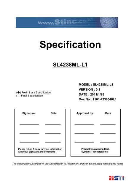
(◆) Preliminary <strong>Specification</strong><br />
( ) Final <strong>Specification</strong><br />
<strong>Specification</strong><br />
<strong>SL4238ML</strong>-<strong>L1</strong><br />
MODEL : <strong>SL4238ML</strong>-<strong>L1</strong><br />
VERSION : 0.1<br />
DATE : 2011/1/28<br />
Doc.No : 1101-4238540<strong>L1</strong><br />
Signature Data Approved by Data<br />
Please return 1 copy for your information<br />
with your signature and comments<br />
Product Engineering Dept.<br />
Systems Technology Inc.<br />
The Information Described in this <strong>Specification</strong> is Preliminary and can be changed without prior notice
<strong>SL4238ML</strong>-<strong>L1</strong><br />
1<br />
2<br />
3<br />
4<br />
5<br />
6<br />
7<br />
8<br />
9<br />
10<br />
No<br />
3-1<br />
3-2<br />
3-3<br />
3-4<br />
3-5<br />
3-6<br />
7-1<br />
7-2<br />
10-1<br />
10-2<br />
10-3<br />
10-4<br />
10-5<br />
10-6<br />
Contents<br />
Revision History<br />
General Description<br />
Absolute Maximum Ratings<br />
Electrical <strong>Specification</strong>s<br />
Electrical Characteristics<br />
Interface Connections<br />
Signal Timing <strong>Specification</strong>s<br />
LVDS Signal <strong>Specification</strong><br />
Color Data Reference<br />
Power Sequence<br />
Optical <strong>Specification</strong><br />
Mechanical Characteristics<br />
Reliability<br />
International standards<br />
Safety<br />
EMC<br />
Packing<br />
Marking & Others<br />
Precautions<br />
Mounting Precautions<br />
Operating Precautions<br />
Storage<br />
Systems Technology Inc.<br />
Contents<br />
Electrostatic Discharge Control<br />
Item<br />
Precautions for Strong Light Exposure<br />
Handling Precautions for Protection Film<br />
<strong>Bar</strong> <strong>LCM</strong> <strong>Specification</strong><br />
Page<br />
Document No.: 1101-4238540<strong>L1</strong> Version 0.1<br />
1<br />
2<br />
3<br />
4<br />
5<br />
7<br />
11<br />
12<br />
15<br />
16<br />
18<br />
22<br />
25<br />
26<br />
27<br />
Page 1 of 32
<strong>SL4238ML</strong>-<strong>L1</strong><br />
Revision History<br />
Date<br />
2011-01-28<br />
Rev.No<br />
0.1<br />
Systems Technology Inc.<br />
Page<br />
<strong>Bar</strong> <strong>LCM</strong> <strong>Specification</strong><br />
Description<br />
Preliminary <strong>Specification</strong>s.<br />
Document No.: 1101-4238540<strong>L1</strong> Version 0.1<br />
Page 2 of 32
<strong>SL4238ML</strong>-<strong>L1</strong><br />
1. General Description<br />
Systems Technology Inc.<br />
<strong>Bar</strong> <strong>LCM</strong> <strong>Specification</strong><br />
The <strong>SL4238ML</strong>-<strong>L1</strong> is a Color Active Matrix Liquid Crystal Display with an integral Light Emitting Diode (LED)<br />
back l light system. The matrix employs a-Si Thin Film Transistor as the active element .<br />
It is a transmissive display type which is operating in the normally black mode. It has a 38 inch diagonally<br />
measured active display area with WUXGA resolution (540 vertical by 1920 horizontal pixel array).<br />
Each pixel is divided into Red, Green and Blue sub-pixels or dots which are arrayed in vertical stripes.<br />
Gray scale or the luminance of the sub-pixel color is determined with a 10-bit gray scale signal for each dot.<br />
Therefore, it can present a palette of more than 1.06Bilion colors.<br />
It has been designed to apply the 10-bit 4-port LVDS interface.<br />
It is intended to support LCD TV, PCTV where high brightness, super wide viewing angle, high color gamut,<br />
high color depth and fast response time are important.<br />
General Information<br />
Interface<br />
Weight<br />
LVDS<br />
2 Port<br />
LVDS 2Port<br />
LVDS select<br />
Bit select<br />
+12V<br />
V_sync<br />
Din<br />
DCLK<br />
Display format<br />
Pixel Pitch<br />
Pixel Format<br />
Color Depth<br />
Luminance, White<br />
CN2<br />
41pin<br />
CN1<br />
51pin<br />
CN3<br />
8pin<br />
Active Display Size<br />
Outline Dimension<br />
Viewing Angle (CR>10)<br />
Power Consumption<br />
Display Operating Mode<br />
Surface Treatment<br />
LVDS 3,4<br />
LVDS 1,2<br />
I2C<br />
+24V , GND , On/Off<br />
Ext VBR-B<br />
Option signal<br />
930.24 mm(H) x 261.63 mm(V)<br />
42inch, 1 / 2 type<br />
973.2 mm(H) x 304.6 mm(V) x 30 mm(D)<br />
0.4845 mm x 0.4845 mm<br />
1920 horiz. by 540 vert. pixels RGB stripe arrangement<br />
LVDS 4Port<br />
10Bit(D) , 1.06 Billion colors<br />
800 cd/m2 (Center 1-point) (Typ.)<br />
Viewing Angle Free ( R/L 178 (Typ.), U/D 178 (Typ))<br />
Total 98W (Typ.) (Logic=10W, LED Driver=88W)<br />
7.0 Kg (Typ)<br />
EEPROM<br />
SCL SDA<br />
Timing Controller<br />
LVDS Rx+OPC+DGA+ODC<br />
Integrated<br />
Power Circuit<br />
Block<br />
LED Driver<br />
Control<br />
Signals<br />
Power Signals<br />
Transmissive mode, Normally black<br />
Mini-LVDS (RGB)<br />
Hard coating (3H),<br />
Anti-glare treatment of the front polarizer (Haze 10%)<br />
Source Driver Circuit<br />
TFT-LCD Panel<br />
(1920 x RGB x 540 pixels)<br />
[ Gate In Panel ]<br />
Document No.: 1101-4238540<strong>L1</strong> Version 0.1<br />
G1<br />
G540<br />
S1 S1920<br />
V : 6 Block<br />
Local Dimming : 12 Block<br />
H : 2 Block<br />
Page 3 of 32
<strong>SL4238ML</strong>-<strong>L1</strong><br />
2. Absolute Maximum Ratings<br />
Systems Technology Inc.<br />
<strong>Bar</strong> <strong>LCM</strong> <strong>Specification</strong><br />
The following items are maximum values which, if exceeded, may cause faulty operation or damage to the<br />
LCD module.<br />
Table 1. Absolute maximum ratings<br />
Driver Control Voltage<br />
Storage Humidity<br />
Parameter<br />
Power Input Voltage<br />
Operating Temperature<br />
Storage Temperature<br />
Panel Front Temperature<br />
Operating Ambient Humidity<br />
-NOTE<br />
1. Ambient temperature condition (Ta = 25 ± 2 °C )<br />
2. Temperature and relative humidity range are shown in the figure below.<br />
Wet bulb temperature should be Max 39°C, and no condensation of water.<br />
3. Gravity mura can be guaranteed below 40°C condition.<br />
4. The maximum operating temperatures is based on the test condition that the surface temperature<br />
of display area is less than or equal to 68°C with LCD module alone in a temperature controlled chamber.<br />
Thermal management should be considered in final product design to prevent the surface temperature of<br />
display area from being over 68℃. The range of operating temperature may degraded in case of<br />
improper thermal management in final product<br />
-20<br />
Wet Bulb<br />
Temperature [℃]<br />
0<br />
0<br />
LCD Circuit<br />
Driver<br />
Brightness<br />
T-Con Option Selection Voltage<br />
10<br />
20<br />
30<br />
Symbol<br />
VLCD<br />
VBL<br />
EXTVBR-B<br />
V LOGIC<br />
T OP<br />
T ST<br />
T SUR<br />
H OP<br />
H ST<br />
40<br />
Document No.: 1101-4238540<strong>L1</strong> Version 0.1<br />
90%<br />
10 20 30 40 50 60 70 80<br />
Dry Bulb Temperature [℃]<br />
50<br />
60<br />
Min<br />
-0.3<br />
-0.3<br />
0.0<br />
-0.3<br />
0<br />
-20<br />
-<br />
10<br />
10<br />
Value<br />
Max<br />
+14.0<br />
+27.0<br />
+5.5<br />
+4.0<br />
+50<br />
+60<br />
+68<br />
90<br />
90<br />
60%<br />
40%<br />
10%<br />
Humidity [(%)RH]<br />
Unit<br />
VDC<br />
VDC<br />
ON / OFF VOFF / VON -0.3 +5.5 VDC<br />
1<br />
VDC<br />
VDC<br />
°C<br />
°C<br />
°C<br />
%RH<br />
%RH<br />
Storage<br />
Operation<br />
Remarks<br />
2 , 3<br />
4<br />
2 , 3<br />
Page 4 of 32
<strong>SL4238ML</strong>-<strong>L1</strong><br />
3. Electrical <strong>Specification</strong>s<br />
3.1. Electrical Characteristics<br />
Systems Technology Inc.<br />
<strong>Bar</strong> <strong>LCM</strong> <strong>Specification</strong><br />
It requires two power inputs. One is employed to power for the LCD circuit. The other Is used for the LED<br />
backlight and LED Driver circuit.<br />
Table 2. Electrical characteristics<br />
Circuit :<br />
Rush current<br />
Note :<br />
Parameter<br />
Power Input Voltage<br />
Power Input Current<br />
Power Consumption<br />
Symbol<br />
V LCD<br />
I LCD<br />
P LCD<br />
I RUSH<br />
1. The specified current and power consumption are under the VLCD=12.0V, Ta=25 ± 2°C, fV=120Hz<br />
condition whereas mosaic pattern(8 x 6) is displayed and fV is the frame frequency.<br />
2. The current is specified at the maximum current pattern.<br />
3. The duration of rush current is about 2ms and rising time of power input is 0.5ms (min.).<br />
Min<br />
10.8<br />
-<br />
-<br />
-<br />
White : 1023 Gray<br />
Black : 0Gray<br />
Value<br />
Typ<br />
12.0<br />
815<br />
1140<br />
9.78<br />
Mosaic Pattern (8 x 3)<br />
Document No.: 1101-4238540<strong>L1</strong> Version 0.1<br />
-<br />
Max<br />
13.2<br />
1060<br />
1482<br />
12.72<br />
5<br />
Unit<br />
VDC<br />
mA<br />
mA<br />
Watt<br />
A<br />
Remarks<br />
1<br />
2<br />
1<br />
3<br />
Page 5 of 32
<strong>SL4238ML</strong>-<strong>L1</strong><br />
Table 3. Electrical characteristics<br />
LED Driver<br />
Power Supply Input Current<br />
LED :<br />
Life Time<br />
Parameter<br />
Power Supply Input Voltage<br />
Power Supply Input Current<br />
(In-Rush)<br />
Power Consumption<br />
On/Off<br />
On<br />
Off<br />
Brightness Adjust<br />
PWM Frequency for<br />
NTSC & PAL<br />
Systems Technology Inc.<br />
Symbol<br />
V BL<br />
IBL_A<br />
Irush<br />
P BL<br />
Von<br />
Voff<br />
ExtV BR-B<br />
PAL<br />
NTSC<br />
<strong>Bar</strong> <strong>LCM</strong> <strong>Specification</strong><br />
Ext VBR-B = 100%<br />
Notes :<br />
1. Electrical characteristics are determined after the unit has been ‘ON’ and stable for approximately 60<br />
minutes at 25±2°C. The specified current and power consumption are under the typical supply Input voltage<br />
24Vand VBR (ExtVBR-B : 100%), it is total power consumption.<br />
2. The life time(MTTF) is determined as the time which luminance of the LED is 50% compared to that of initial<br />
value at the typical LED current (ExtVBR-B :100%) on condition of continuous operating in <strong>LCM</strong> state at<br />
25±2°C.<br />
3. LGD recommend that the PWM freq. is synchronized with One time harmonic of Vsync signal of system.<br />
Though PWM frequency is over 120Hz (max 252Hz), function of LED Driver is not affected.<br />
4. The duration of rush current is about 10ms.<br />
5. Even though inrush current is over the specified value, there is no problem if I 2 T spec of fuse is satisfied.<br />
Min<br />
22.8<br />
-<br />
-<br />
-<br />
2.5<br />
-0.3<br />
10<br />
30,000<br />
Values<br />
Typ<br />
24.0<br />
Document No.: 1101-4238540<strong>L1</strong> Version 0.1<br />
3.7<br />
-<br />
88<br />
-<br />
0.0<br />
-<br />
100<br />
120<br />
50,000<br />
Max<br />
25.2<br />
4.0<br />
6.5<br />
94.1<br />
5.0<br />
0.7<br />
100<br />
Unit<br />
Vdc<br />
A<br />
A<br />
W<br />
Vdc<br />
Vdc<br />
%<br />
Hz<br />
Hz<br />
Hrs<br />
V BL = 22.8V<br />
ExtV BR_B = 100%<br />
4<br />
V BR-B = 100%<br />
On Duty<br />
Remarks<br />
1<br />
3<br />
3<br />
2<br />
Page 6 of 32
No.<br />
1<br />
2<br />
3<br />
4<br />
5<br />
6<br />
7<br />
8<br />
9<br />
10<br />
11<br />
12<br />
13<br />
14<br />
15<br />
16<br />
17<br />
18<br />
19<br />
20<br />
21<br />
22<br />
23<br />
24<br />
25<br />
26<br />
<strong>SL4238ML</strong>-<strong>L1</strong><br />
3.2. Interface connections<br />
Table 4-1. Module connector(CN1) pin configuration<br />
Systems Technology Inc.<br />
<strong>Bar</strong> <strong>LCM</strong> <strong>Specification</strong><br />
This LCD module employs two kinds of interface connection, 51-pin connector and 41-pin connector are used<br />
for the module electronics and 14-pin connector is used for the integral backlight system.<br />
3.2.1 LCD Module<br />
- LCD Connector : FI-R51S-HF(manufactured by JAE) or KN25-51P-0.5SH(manufactured by Hirose)<br />
(CN1) Refer to below and next Page table<br />
- Mating Connector : FI-R51HL(JAE) or compatible<br />
Symbol<br />
NC<br />
NC<br />
NC<br />
NC<br />
NC<br />
NC<br />
LVDS Select<br />
NC<br />
NC<br />
L-DIM Enable<br />
GND<br />
R1AN<br />
R1AP<br />
R1BN<br />
R1BP<br />
R1CN<br />
R1CP<br />
GND<br />
R1CLKN<br />
R1CLKP<br />
GND<br />
R1DN<br />
R1DP<br />
R1EN<br />
R1EP<br />
NC<br />
No Connection<br />
No Connection<br />
No Connection<br />
No Connection<br />
No Connection<br />
No Connection<br />
‘H’ = JEIDA, ‘L’ or NC = VESA<br />
No Connection<br />
No Connection<br />
‘H’ = Enable, ‘L’ or NC = Disable<br />
Ground<br />
FIRST LVDS Receiver Signal (A-)<br />
FIRST LVDS Receiver Signal (A+)<br />
FIRST LVDS Receiver Signal (B-)<br />
FIRST LVDS Receiver Signal (B+)<br />
FIRST LVDS Receiver Signal (C-)<br />
FIRST LVDS Receiver Signal (C+)<br />
Ground<br />
FIRST LVDS Receiver Clock Signal(-)<br />
FIRST LVDS Receiver Clock Signal(+)<br />
Ground<br />
FIRST LVDS Receiver Signal (D-)<br />
FIRST LVDS Receiver Signal (D+)<br />
FIRST LVDS Receiver Signal (E-)<br />
FIRST LVDS Receiver Signal (E+)<br />
No Connection<br />
Description<br />
No.<br />
27<br />
28<br />
29<br />
30<br />
31<br />
32<br />
33<br />
34<br />
35<br />
36<br />
37<br />
38<br />
39<br />
40<br />
41<br />
42<br />
43<br />
44<br />
45<br />
46<br />
47<br />
48<br />
49<br />
50<br />
51<br />
-<br />
Symbol<br />
Bit Select<br />
R2AN<br />
R2AP<br />
R2BN<br />
R2BP<br />
R2CN<br />
R2CP<br />
R2DP<br />
R2EN<br />
R2EP<br />
VLCD<br />
VLCD<br />
VLCD<br />
VLCD<br />
Document No.: 1101-4238540<strong>L1</strong> Version 0.1<br />
GND<br />
R2CLKN<br />
R2CLKP<br />
GND<br />
R2DN<br />
NC<br />
NC<br />
GND<br />
GND<br />
GND<br />
NC<br />
-<br />
SECOND LVDS Receiver Signal (A-)<br />
SECOND LVDS Receiver Signal (A+)<br />
SECOND LVDS Receiver Signal (B-)<br />
SECOND LVDS Receiver Signal (B+)<br />
SECOND LVDS Receiver Signal (C-)<br />
SECOND LVDS Receiver Signal (C+)<br />
Ground<br />
SECOND LVDS Receiver Clock Signal(-)<br />
SECOND LVDS Receiver Clock Signal(+)<br />
Ground<br />
SECOND LVDS Receiver Signal (D-)<br />
SECOND LVDS Receiver Signal (D+)<br />
SECOND LVDS Receiver Signal (E-)<br />
SECOND LVDS Receiver Signal (E+)<br />
No Connection<br />
No Connection<br />
Ground<br />
Ground<br />
Ground<br />
No connection<br />
Description<br />
H’ or NC= 10bit(D) , ‘L’ = 8bit<br />
Power Supply +12.0V<br />
Power Supply +12.0V<br />
Power Supply +12.0V<br />
Power Supply +12.0V<br />
-<br />
Page 7 of 32
<strong>SL4238ML</strong>-<strong>L1</strong><br />
Systems Technology Inc.<br />
<strong>Bar</strong> <strong>LCM</strong> <strong>Specification</strong><br />
Notes :<br />
1. All GND(ground) pins should be connected together to the LCD module’s metal frame.<br />
2. All VLCD (power input) pins should be connected together.<br />
3. All Input levels of LVDS signals are based on the EIA 644 Standard.<br />
4. Specific pins (pin No. #2~#6) are used for internal data process of the LCD module.<br />
These pins should be no connection.<br />
5. Specific pins (pin No. #10) are used for Local Dimming function of the LCD module.<br />
If not used, these pins are no connection. (Please see the Appendix III-4 for more information.)<br />
6. LVDS pin (pin No. #24,25,40,41) are used for 10Bit(D) of the LCD module.<br />
If used for 8Bit(R), these pins are no connection.<br />
7. Specific pin No. #44 is used for “No signal detection” of system signal interface.<br />
It should be GND for NSB (No Signal Black) during the system interface signal is not.<br />
If this pin is “H”, LCD Module displays AGP (Auto Generation Pattern).<br />
Document No.: 1101-4238540<strong>L1</strong> Version 0.1<br />
Page 8 of 32
No.<br />
1<br />
2<br />
3<br />
4<br />
5<br />
6<br />
7<br />
8<br />
9<br />
10<br />
11<br />
12<br />
13<br />
14<br />
15<br />
16<br />
17<br />
18<br />
19<br />
20<br />
21<br />
<strong>SL4238ML</strong>-<strong>L1</strong><br />
Table 4-2. Module connector(CN2) pin configuration<br />
Symbol<br />
NC<br />
NC<br />
NC<br />
NC<br />
NC<br />
NC<br />
NC<br />
NC<br />
GND<br />
RA3N<br />
RA3P<br />
RB3N<br />
RB3P<br />
RC3N<br />
RC3P<br />
GND<br />
RCLK3N<br />
RCLK3P<br />
GND<br />
RD3N<br />
RD3P<br />
No Connection<br />
No Connection<br />
No Connection<br />
No Connection<br />
No Connection<br />
No Connection<br />
No Connection<br />
Ground<br />
THIRD LVDS Receiver Signal (A-)<br />
THIRD LVDS Receiver Signal (A+)<br />
THIRD LVDS Receiver Signal (B-)<br />
THIRD LVDS Receiver Signal (B+)<br />
THIRD LVDS Receiver Signal (C-)<br />
THIRD LVDS Receiver Signal (C+)<br />
Ground<br />
THIRD LVDS Receiver Clock Signal(-)<br />
THIRD LVDS Receiver Clock Signal(+)<br />
Ground<br />
Description<br />
No connection (Reserved)<br />
THIRD LVDS Receiver Signal (D-)<br />
THIRD LVDS Receiver Signal (D+)<br />
Systems Technology Inc.<br />
<strong>Bar</strong> <strong>LCM</strong> <strong>Specification</strong><br />
-LCD Connector : FI-RE41S-HF (manufactured by JAE) or KN25-41P-0.5SH (manufactured by Hirose)<br />
(CN2)<br />
- Mating Connector : FI-RE41HL<br />
22<br />
23<br />
24<br />
25<br />
26<br />
27<br />
28<br />
29<br />
30<br />
31<br />
32<br />
33<br />
34<br />
35<br />
36<br />
37<br />
38<br />
39<br />
40<br />
41<br />
-<br />
Symbol<br />
RE3N<br />
RE3P<br />
RA4N<br />
RA4P<br />
RB4N<br />
RB4P<br />
RC4N<br />
RC4P<br />
RCLK4N<br />
RCLK4P<br />
RD4N<br />
RD4P<br />
RE4N<br />
RE4P<br />
Notes :<br />
1. All GND(ground) pins should be connected together to the LCD module’s metal frame.<br />
2. LVDS pin (pin No. #22,23,38,39) are used for 10Bit(D) of the LCD module.<br />
If used for 8Bit(R), these pins are no connection.<br />
Table 4-3. Module connector(CN3) pin configuration<br />
No.<br />
1<br />
2<br />
3<br />
4<br />
5<br />
6<br />
7<br />
8<br />
Symbol<br />
VSYNC<br />
GND<br />
GND<br />
SIN<br />
GND<br />
SCLK<br />
Reserved<br />
Reverse<br />
Vertical Sync signal<br />
Backlight Ground<br />
Backlight Ground<br />
Backlight Ground<br />
No Connection<br />
Description<br />
Local Dimming Serial Data<br />
Local Dim Serial Clock<br />
Local Dimming data Reverse<br />
No.<br />
Ground<br />
Document No.: 1101-4238540<strong>L1</strong> Version 0.1<br />
GND<br />
GND<br />
GND<br />
GND<br />
GND<br />
GND<br />
THIRD LVDS Receiver Signal (E-)<br />
THIRD LVDS Receiver Signal (E+)<br />
Ground<br />
Ground<br />
FORTH LVDS Receiver Signal (A-)<br />
FORTH LVDS Receiver Signal (A+)<br />
FORTH LVDS Receiver Signal (B-)<br />
FORTH LVDS Receiver Signal (B+)<br />
FORTH LVDS Receiver Signal (C-)<br />
FORTH LVDS Receiver Signal (C+)<br />
Ground<br />
FORTH LVDS Receiver Clock Signal(-)<br />
FORTH LVDS Receiver Clock Signal(+)<br />
Ground<br />
FORTH LVDS Receiver Signal (D-)<br />
FORTH LVDS Receiver Signal (D+)<br />
FORTH LVDS Receiver Signal (E-)<br />
FORTH LVDS Receiver Signal (E+)<br />
Ground<br />
Description<br />
Page 9 of 32
<strong>SL4238ML</strong>-<strong>L1</strong><br />
3.2.2 LCD Module<br />
Master<br />
- LED Driver Connector : 20022WR-14B1(Yeonho)<br />
or Equivalent<br />
- Mating Connector : 20022HS-14 or Equivalent<br />
Table 5. LED DRIVER CONNECTOR PIN CONFIGURATION<br />
No.<br />
1<br />
2<br />
3<br />
4<br />
5<br />
6<br />
7<br />
8<br />
9<br />
10<br />
11<br />
12<br />
13<br />
14<br />
Symbol<br />
VBL<br />
VBL<br />
VBL<br />
VBL<br />
VBL<br />
GND<br />
GND<br />
GND<br />
GND<br />
GND<br />
NC<br />
Von / off<br />
EXT VBR-B<br />
NC<br />
No connection<br />
External PWM<br />
No connection<br />
Systems Technology Inc.<br />
Backlight Ground<br />
Backlight Ground<br />
Backlight Ground<br />
Backlight Ground<br />
Backlight Ground<br />
Description<br />
Power Supply +24.0V<br />
Power Supply +24.0V<br />
Power Supply +24.0V<br />
Power Supply +24.0V<br />
Power Supply +24.0V<br />
Backlight ON / OFF control<br />
<strong>Bar</strong> <strong>LCM</strong> <strong>Specification</strong><br />
GND<br />
GND<br />
GND<br />
GND<br />
GND<br />
OPEN or GND<br />
Von / off<br />
EXT VBR-B<br />
OPEN or GND<br />
Notes :<br />
1. GND should be connected to the LCD module’s metal frame.<br />
2. High : on duty / Low : off duty, Pin#13 can be opened. ( if Pin #13 is open , EXTVBR-B is 100% )<br />
3. Each impedance of pin #12 and 13 is over 50 [KΩ].<br />
■ Rear view of <strong>LCM</strong><br />
< Master ><br />
Document No.: 1101-4238540<strong>L1</strong> Version 0.1<br />
VBL<br />
VBL<br />
VBL<br />
VBL<br />
VBL<br />
1<br />
2<br />
TBD<br />
Page 10 of 32
<strong>SL4238ML</strong>-<strong>L1</strong><br />
3.3 Signal Timing <strong>Specification</strong>s<br />
Systems Technology Inc.<br />
<strong>Bar</strong> <strong>LCM</strong> <strong>Specification</strong><br />
Table 6 shows the signal timing required at the input of the LVDS transmitter. All of the interface signal<br />
timings should be satisfied with the following specification for normal operation.<br />
Table 6-1. TIMING TABLE for NTSC (DE Only Mode)<br />
Horizontal<br />
Vertical<br />
Frequency<br />
ITEM<br />
Display Period<br />
Display Period<br />
ITEM<br />
Blank<br />
Total<br />
Blank<br />
Total<br />
DCLK<br />
Horizontal<br />
Vertical<br />
Symbol<br />
tHV<br />
tHB<br />
tHP<br />
tVV<br />
tVB<br />
tVP<br />
Symbol<br />
fCLK<br />
Min<br />
480<br />
40<br />
520<br />
1080<br />
16<br />
1096<br />
Min<br />
66.97<br />
121.8<br />
108<br />
Table 6-2. TIMING TABLE for DVE / PAL (DE Only Mode)<br />
Horizontal<br />
Vertical<br />
Frequency<br />
ITEM<br />
Display Period<br />
Display Period<br />
ITEM<br />
Blank<br />
Total<br />
Blank<br />
Total<br />
DCLK<br />
Horizontal<br />
Vertical<br />
fH<br />
fV<br />
Symbol<br />
tHV<br />
tHB<br />
tHP<br />
tVV<br />
tVB<br />
tVP<br />
Symbol<br />
fCLK<br />
fH<br />
fV<br />
Min<br />
480<br />
40<br />
520<br />
1080<br />
228<br />
1308<br />
Min<br />
66.97<br />
121.8<br />
95<br />
Typ<br />
480<br />
70<br />
550<br />
1080<br />
45<br />
1125<br />
Typ<br />
74.25<br />
135<br />
120<br />
Typ<br />
480<br />
70<br />
550<br />
1080<br />
270<br />
1350<br />
74.25<br />
Lines<br />
Lines<br />
Lines<br />
1920/4<br />
Document No.: 1101-4238540<strong>L1</strong> Version 0.1<br />
Max<br />
480<br />
200<br />
680<br />
1080<br />
86<br />
1166<br />
Max<br />
78.00<br />
140<br />
122<br />
Max<br />
480<br />
200<br />
680<br />
1080<br />
300<br />
1380<br />
78.00<br />
Unit<br />
tclk<br />
tclk<br />
tclk<br />
Unit<br />
MHz<br />
KHz<br />
Hz<br />
Unit<br />
tclk<br />
tclk<br />
tclk<br />
Lines<br />
Lines<br />
Lines<br />
Note :<br />
1. The Input of HSYNC & VSYNC signal does not have an effect on normal operation(DE Only Mode).<br />
If you use spread spectrum for EMI, add some additional clock to minimum value for clock margin.<br />
2. The performance of the electro-optical characteristics may be influenced by variance of the vertical<br />
refresh rate and the horizontal frequency.<br />
Typ<br />
135<br />
100<br />
Max<br />
140<br />
104<br />
Unit<br />
MHz<br />
KHz<br />
Hz<br />
Note<br />
1<br />
Note<br />
2<br />
2<br />
Note<br />
1920/4<br />
1<br />
Note<br />
148.5/2<br />
Page 11 of 32
<strong>SL4238ML</strong>-<strong>L1</strong><br />
3.4. LVDS Signal <strong>Specification</strong><br />
3.4.1 LVDS Input Signal Timing Diagram<br />
Systems Technology Inc.<br />
<strong>Bar</strong> <strong>LCM</strong> <strong>Specification</strong><br />
Document No.: 1101-4238540<strong>L1</strong> Version 0.1<br />
Page 12 of 32
<strong>SL4238ML</strong>-<strong>L1</strong><br />
3.4.2 LVDS Input Signal Characteristics<br />
1) DC <strong>Specification</strong><br />
Description<br />
LVDS Common mode Voltage<br />
LVDS Input Voltage Range<br />
Systems Technology Inc.<br />
<strong>Bar</strong> <strong>LCM</strong> <strong>Specification</strong><br />
Change in common mode Voltage △VCM<br />
-<br />
250<br />
mV<br />
-<br />
2) AC <strong>Specification</strong><br />
LVDS Clock/DATA Rising/Falling time<br />
Effective time of LVDS<br />
Description<br />
LVDS Differential Voltage<br />
LVDS Clock to Data Skew Margin<br />
Symbol<br />
VCM<br />
VIN<br />
High Threshold<br />
Low Threshold<br />
Min<br />
1.0<br />
0.7<br />
Symbol<br />
VTH<br />
VTL<br />
tSKEW<br />
tRF<br />
teff<br />
Document No.: 1101-4238540<strong>L1</strong> Version 0.1<br />
Max<br />
1.5<br />
1.8<br />
-<br />
260<br />
±360<br />
Unit<br />
V<br />
V<br />
/(0.25*Tclk)/7/<br />
(0.3*Tclk)/7<br />
LVDS Clock to Clock Skew Margin (Even to Odd) tSKEW_EO<br />
-<br />
1/7*Tclk Tclk -<br />
Note :<br />
1. All Input levels of LVDS signals are based on the EIA 644 Standard.<br />
2. If tRF isn’t enough, teff should be meet the range.<br />
3. LVDS Differential Voltage is defined within teff<br />
Min<br />
100<br />
-300<br />
Max<br />
300<br />
-100<br />
-<br />
Unit<br />
mV<br />
mV<br />
ps<br />
ps<br />
ps<br />
Note<br />
Page 13 of 32<br />
-<br />
-<br />
Note<br />
3<br />
-<br />
2<br />
-
<strong>SL4238ML</strong>-<strong>L1</strong><br />
Systems Technology Inc.<br />
<strong>Bar</strong> <strong>LCM</strong> <strong>Specification</strong><br />
Document No.: 1101-4238540<strong>L1</strong> Version 0.1<br />
Page 14 of 32
<strong>SL4238ML</strong>-<strong>L1</strong><br />
Table 7. Color Data Reference<br />
Basic<br />
Color<br />
RED<br />
GREEN<br />
BLUE<br />
3.5 Color Data Reference<br />
Systems Technology Inc.<br />
<strong>Bar</strong> <strong>LCM</strong> <strong>Specification</strong><br />
The brightness of each primary color (red,green,blue) is based on the 10-bit gray scale data input for the color.<br />
The higher binary input, the brighter the color. Table 7 provides a reference for color versus data input.<br />
Color<br />
Black<br />
Red (1023)<br />
Green (1023)<br />
Blue (1023)<br />
Cyan<br />
Magenta<br />
Yellow<br />
White<br />
RED (000)<br />
RED (001)<br />
...<br />
RED (1022)<br />
RED (1023)<br />
GREEN (000)<br />
GREEN (001)<br />
...<br />
GREEN (1022)<br />
GREEN (1023)<br />
BLUE (000)<br />
BLUE (001)<br />
...<br />
BLUE (1022)<br />
BLUE (1023)<br />
RED<br />
MSB LSB<br />
R9 R8 R7 R6 R5 R4 R3 R2 R1 R0<br />
0 0 0 0 0 0 0 0 0 0<br />
1 1 1 1 1 1 1 1 1 1<br />
0 0 0 0 0 0 0 0 0 0<br />
0 0 0 0 0 0 0 0 0 0<br />
0 0 0 0 0 0 0 0 0 0<br />
1 1 1 1 1 1 1 1 1 1<br />
1 1 1 1 1 1 1 1 1 1<br />
1 1 1 1 1 1 1 1 1 1<br />
0 0 0 0 0 0 0 0 0 0<br />
0 0 0 0 0 0 0 0 0 1<br />
...<br />
1 1 1 1 1 1 1 1 1 0<br />
1 1 1 1 1 1 1 1 1 1<br />
0 0 0 0 0 0 0 0 0 0<br />
0 0 0 0 0 0 0 0 0 0<br />
...<br />
0 0 0 0 0 0 0 0 0 0<br />
0 0 0 0 0 0 0 0 0 0<br />
0 0 0 0 0 0 0 0 0 0<br />
0 0 0 0 0 0 0 0 0 0<br />
...<br />
0 0 0 0 0 0 0 0 0 0<br />
0 0 0 0 0 0 0 0 0 0<br />
Input Color Data<br />
GREEN<br />
MSB LSB<br />
G9 G8 G7 G6 G5 G4 G3 G2 G1 G0<br />
0 0 0 0 0 0 0 0 0 0<br />
0 0 0 0 0 0 0 0 0 0<br />
1 1 1 1 1 1 1 1 1 1<br />
0 0 0 0 0 0 0 0 0 0<br />
1 1 1 1 1 1 1 1 1 1<br />
0 0 0 0 0 0 0 0 0 0<br />
1 1 1 1 1 1 1 1 1 1<br />
1 1 1 1 1 1 1 1 1 1<br />
0 0 0 0 0 0 0 0 0 0<br />
0 0 0 0 0 0 0 0 0 0<br />
0 0 0 0 0 0 0 0 0 0<br />
0 0 0 0 0 0 0 0 0 0<br />
0 0 0 0 0 0 0 0 0 0<br />
0 0 0 0 0 0 0 0 0 1<br />
1 1 1 1 1 1 1 1 1 0<br />
1 1 1 1 1 1 1 1 1 1<br />
0 0 0 0 0 0 0 0 0 0<br />
0 0 0 0 0 0 0 0 0 0<br />
0 0 0 0 0 0 0 0 0 0<br />
0 0 0 0 0 0 0 0 0 0<br />
1 1 1 1 1 1 1 1 1 0<br />
1 1 1 1 1 1 1 1 1 1<br />
Document No.: 1101-4238540<strong>L1</strong> Version 0.1<br />
...<br />
...<br />
...<br />
BLUE<br />
MSB LSB<br />
B9 B8 B7 B6 B5 B4 B3 B2 B1 B0<br />
0 0 0 0 0 0 0 0 0 0<br />
0 0 0 0 0 0 0 0 0 0<br />
0 0 0 0 0 0 0 0 0 0<br />
1 1 1 1 1 1 1 1 1 1<br />
1 1 1 1 1 1 1 1 1 1<br />
1 1 1 1 1 1 1 1 1 1<br />
0 0 0 0 0 0 0 0 0 0<br />
1 1 1 1 1 1 1 1 1 1<br />
0 0 0 0 0 0 0 0 0 0<br />
0 0 0 0 0 0 0 0 0 0<br />
...<br />
0 0 0 0 0 0 0 0 0 0<br />
0 0 0 0 0 0 0 0 0 0<br />
0 0 0 0 0 0 0 0 0 0<br />
0 0 0 0 0 0 0 0 0 0<br />
...<br />
0 0 0 0 0 0 0 0 0 0<br />
0 0 0 0 0 0 0 0 0 0<br />
0 0 0 0 0 0 0 0 0 0<br />
0 0 0 0 0 0 0 0 0 1<br />
...<br />
Page 15 of 32
<strong>SL4238ML</strong>-<strong>L1</strong><br />
3.6. Power Sequence<br />
3.6.1. LCD Driving circuit<br />
Table 8. POWER SEQUENCE<br />
Parameter<br />
T1<br />
T2<br />
T3<br />
T4<br />
T5<br />
T6<br />
T7<br />
T8<br />
Min<br />
0.5<br />
0<br />
200<br />
200<br />
1.0<br />
-<br />
0.5<br />
100<br />
Systems Technology Inc.<br />
Value<br />
Typ<br />
-<br />
-<br />
-<br />
-<br />
-<br />
-<br />
-<br />
-<br />
<strong>Bar</strong> <strong>LCM</strong> <strong>Specification</strong><br />
Document No.: 1101-4238540<strong>L1</strong> Version 0.1<br />
Max<br />
20<br />
-<br />
-<br />
-<br />
-<br />
-<br />
T2<br />
-<br />
ms<br />
ms<br />
ms<br />
ms<br />
s<br />
ms<br />
s<br />
ms<br />
Remarks<br />
Note :<br />
1. Please avoid floating state of interface signal at invalid period.<br />
2. When the power supply for LCD (VLCD) is off, be sure to pull down the valid and invalid data to 0V.<br />
3. The T3 / T4 is recommended value, the case when failed to meet a minimum specification,<br />
abnormal display would be shown. There is no reliability problem.<br />
4. If the on time of signals (Interface signal and user control signals) precedes the on time of Power (VLCD),<br />
it will be happened abnormal display. When T6 is NC status, T6 doesn’t need to be measured.<br />
5. T5 should be measured after the Module has been fully discharged between power off and on<br />
period.<br />
6. It is recommendation specification that T8 has to be 100ms as a minimum value.<br />
Unit<br />
4<br />
3<br />
3<br />
5<br />
4<br />
6<br />
Page 16 of 32
<strong>SL4238ML</strong>-<strong>L1</strong><br />
3.6.2. Sequence for LED Driver<br />
Power Supply For LED Driver<br />
3.6.3. Dip condition for LED Driver<br />
VBL(Typ.) x 0.8<br />
Table 9. Power Sequence for LED Driver<br />
Parameter<br />
T1<br />
T2<br />
T3<br />
T4<br />
T5<br />
T6<br />
Min<br />
20<br />
500<br />
10<br />
Systems Technology Inc.<br />
0<br />
0<br />
-<br />
Values<br />
Typ<br />
-<br />
-<br />
-<br />
-<br />
-<br />
T6<br />
Max<br />
<strong>Bar</strong> <strong>LCM</strong> <strong>Specification</strong><br />
VBL : 24V<br />
Document No.: 1101-4238540<strong>L1</strong> Version 0.1<br />
-<br />
-<br />
-<br />
-<br />
-<br />
10<br />
Units<br />
ms<br />
ms<br />
ms<br />
ms<br />
ms<br />
ms<br />
0V<br />
Remarks<br />
1<br />
V BL (Typ) x 0.8<br />
Notes :<br />
1. T1 describes rising time of 0V to 24V and this parameter does not applied at restarting time.<br />
Even though T1 is over the specified value, there is no problem if I2T spec of fuse is satisfied.<br />
Page 17 of 32
<strong>SL4238ML</strong>-<strong>L1</strong><br />
4. Optical specification<br />
Systems Technology Inc.<br />
<strong>Bar</strong> <strong>LCM</strong> <strong>Specification</strong><br />
Optical characteristics are determined after the unit has been ‘ON’ and stable in a dark environment at 25±2°C.<br />
The values are specified at an approximate distance 50cm from the LCD surface at a viewing angle of Φ and θ<br />
equal to 0 °.<br />
FIG. 1 shows additional information concerning the measurement equipment and method.<br />
Table 10. Optical characteristics<br />
Surface Luminance, white<br />
Luminance Variation<br />
Response<br />
Time<br />
Color<br />
Coordinates<br />
[CIE1931]<br />
Color Temperature<br />
Uniformity<br />
Color Gamut (CIE1931 NTSC)<br />
Viewing Angle (CR>10)<br />
Gray Scale<br />
Optical Stage(x,y)<br />
Parameter<br />
Gray-to- Gray<br />
MPRT<br />
Uniformity<br />
RED<br />
GREEN<br />
BLUE<br />
WHITE<br />
x axis, right(φ=0°)<br />
x axis, left (φ=180°)<br />
y axis, up (φ=90°)<br />
y axis, down (φ=270°)<br />
LCD Module<br />
Ta=25±2°C,VLCD=12.0V,fV=120Hz,Dclk=74.25MHz,EXTVBR_B=100%<br />
Contrast Ratio CR 1000 1400 -<br />
L WH<br />
δ WHITE<br />
δ MPRT<br />
δ G TO G<br />
Rx<br />
Ry<br />
Gx<br />
Gy<br />
Bx<br />
By<br />
Wx<br />
Wy<br />
θr<br />
θl<br />
θu<br />
θd<br />
1°<br />
Symbol<br />
G to G<br />
MPRT<br />
5P<br />
Min<br />
600<br />
-<br />
-<br />
-<br />
-<br />
-<br />
Typ<br />
-0.03<br />
89<br />
89<br />
89<br />
89<br />
-<br />
Value<br />
Document No.: 1101-4238540<strong>L1</strong> Version 0.1<br />
Typ<br />
800<br />
-<br />
5<br />
8<br />
-<br />
-<br />
0.647<br />
0.332<br />
0.309<br />
0.601<br />
0.149<br />
0.059<br />
0.279<br />
0.292<br />
10,000<br />
72<br />
-<br />
-<br />
-<br />
-<br />
-<br />
BM7 or<br />
equivalent<br />
50cm<br />
FIG. 1 Optical Characteristic Measurement Equipment and Method<br />
Max<br />
1.3<br />
8<br />
12<br />
1<br />
1<br />
Typ<br />
+0.03<br />
K<br />
%<br />
-<br />
-<br />
-<br />
-<br />
-<br />
Unit<br />
cd/m 2<br />
ms<br />
ms<br />
degree<br />
Remarks<br />
1<br />
2<br />
3<br />
4,5<br />
6<br />
7<br />
Page 18 of 32
<strong>SL4238ML</strong>-<strong>L1</strong><br />
Systems Technology Inc.<br />
<strong>Bar</strong> <strong>LCM</strong> <strong>Specification</strong><br />
Notes : 1. Contrast Ratio(CR) is defined mathematically as :<br />
Contrast Ratio = (Surface Luminance with all white pixels) / (Surface Luminance with all black pixels)<br />
It is measured at center 1-point.<br />
2. Surface luminance are determined after the unit has been ‘ON’ and 1 Hour after lighting the backlight in a dark<br />
environment at 25±2°C. Surface luminance is the luminance value at center 1-point across the LCD surface<br />
50cm<br />
from the surface with all pixels displaying white.<br />
For more information see the FIG. 2.<br />
3. The variation in surface luminance , δ WHITE is defined as :<br />
δ WHITE(5P) = Maximum(Lon1,Lon2, Lon3, Lon4, Lon5) / Minimum(Lon1,Lon2, Lon3, Lon4, Lon5)<br />
Where Lon1 to Lon5 are the luminance with all pixels displaying white at 5 locations .<br />
For more information, see the FIG. 2.<br />
4. Response time is the time required for the display to transit from G(N) to G(M) (Rise Time, TrR) and from G(M) to<br />
G(N) (Decay Time, TrD). For additional information see the FIG. 3. (N
<strong>SL4238ML</strong>-<strong>L1</strong><br />
Measuring point for surface luminance & luminance variation<br />
V<br />
B<br />
Response time is defined as the following figure and shall be measured by switching the input<br />
signal for “Gray(N)” and “Gray(M)”.<br />
100<br />
90<br />
Optical<br />
Response<br />
10<br />
0<br />
②<br />
④<br />
Gray(N)<br />
A<br />
Systems Technology Inc.<br />
H<br />
①<br />
FIG.2 5 Points for Luminance Measure<br />
TrR TrD<br />
Gray(M)<br />
③<br />
⑤<br />
N,M = (Black)~(White), N
<strong>SL4238ML</strong>-<strong>L1</strong><br />
Systems Technology Inc.<br />
<strong>Bar</strong> <strong>LCM</strong> <strong>Specification</strong><br />
MPRT is defined as the 10% to 90% blur-edge with Bij(pixels) and scroll speed U(pixels / frame) at the moving<br />
picture.<br />
Example)<br />
Bij = 12 pixels, U = 10 pixels / 120 Hz<br />
M = 12 pixels / (10 pixels / 120Hz)<br />
= 12 pixels / (10 pixels / (1/120)s)<br />
= 12 / 1,200 s<br />
= 10 ms<br />
Dimension of viewing angle range<br />
Φ=180 °, LEFT<br />
Φ=270 °, DOWN<br />
FIG. 4 MPRT<br />
NORMAL<br />
θ<br />
Φ<br />
E<br />
FIG. 5 Viewing Angle<br />
Φ=90 °, UP<br />
Φ=0 °, RIGHT<br />
Document No.: 1101-4238540<strong>L1</strong> Version 0.1<br />
Y<br />
Page 21 of 32
<strong>SL4238ML</strong>-<strong>L1</strong><br />
5. Mechanical Characteristics<br />
Table 12 provides general mechanical characteristics.<br />
Table 12. MECHANICAL CHARACTERISTICS<br />
Bezel Area<br />
Weight<br />
Item<br />
Outline Dimension<br />
Active Display Area<br />
Systems Technology Inc.<br />
Horizontal<br />
Vertical<br />
Depth<br />
Horizontal<br />
Vertical<br />
Horizontal<br />
Vertical<br />
7.0 Kg<br />
<strong>Bar</strong> <strong>LCM</strong> <strong>Specification</strong><br />
Value<br />
973.2 mm<br />
304.6 mm<br />
30.0 mm<br />
937.2 mm<br />
268.6 mm<br />
930.24 mm<br />
261.62 mm<br />
Notes :<br />
Please refer to a mechanic drawing in terms of tolerance at the next page.<br />
Document No.: 1101-4238540<strong>L1</strong> Version 0.1<br />
Page 22 of 32
<strong>SL4238ML</strong>-<strong>L1</strong><br />
<br />
Systems Technology Inc.<br />
<strong>Bar</strong> <strong>LCM</strong> <strong>Specification</strong><br />
Document No.: 1101-4238540<strong>L1</strong> Version 0.1<br />
Page 23 of 32
<strong>SL4238ML</strong>-<strong>L1</strong><br />
<br />
Systems Technology Inc.<br />
<strong>Bar</strong> <strong>LCM</strong> <strong>Specification</strong><br />
Document No.: 1101-4238540<strong>L1</strong> Version 0.1<br />
Page 24 of 32
<strong>SL4238ML</strong>-<strong>L1</strong><br />
6. Reliability<br />
Table 13. Environment test conditions<br />
No.<br />
1<br />
2<br />
3<br />
4<br />
5<br />
6<br />
7<br />
8<br />
Notes :<br />
Altitude<br />
operating<br />
storage / shipment<br />
0 - 15,000 ft<br />
0 - 40,000 ft<br />
1. Before and after Reliability test, <strong>LCM</strong> should be operated with normal function.<br />
7. International standard<br />
7.1. Safety<br />
TBD<br />
7.2. EMC<br />
TBD<br />
8. Packing<br />
Shock test<br />
(non-operation)<br />
TBD<br />
9. Marking & Others<br />
TBD<br />
Vibration test<br />
Test Item<br />
High temperature storage test<br />
Low temperature storage test<br />
High temperature operation test<br />
Low temperature operation test<br />
Humidity condition Operation<br />
Systems Technology Inc.<br />
Ta= 40°C 90%RH<br />
<strong>Bar</strong> <strong>LCM</strong> <strong>Specification</strong><br />
Condition<br />
Ta= 60°C 240h<br />
Ta= -20°C 240h<br />
Ta= 50°C 50%RH 240h<br />
Ta= 0°C 240h<br />
Wave form : random<br />
Vibration level : 1.0Grms<br />
Bandwidth : 10-300Hz<br />
Duration : X,Y,Z 30 min<br />
Each direction per 10 min<br />
Shock level :50G(X,Y axis) , 35G(Z axis)<br />
Waveform : half sine wave, 11ms<br />
Direction : ±X, ±Y, ±Z<br />
One time each direction<br />
Document No.: 1101-4238540<strong>L1</strong> Version 0.1<br />
Page 25 of 32
<strong>SL4238ML</strong>-<strong>L1</strong><br />
10. Precautions<br />
Please pay attention to the followings when you use this TFT LCD module.<br />
10-1. Mounting Precautions<br />
Systems Technology Inc.<br />
<strong>Bar</strong> <strong>LCM</strong> <strong>Specification</strong><br />
(1) You must mount a module using specified mounting holes (Details refer to the drawings).<br />
(2) You should consider the mounting structure so that uneven force (ex. Twisted stress) is<br />
not applied to the Module. And the case on which a module is mounted should have<br />
sufficient strength so that external force is not transmitted directly to the module.<br />
(3) Please attach the surface transparent protective plate to the surface in order to protect<br />
the polarizer. Transparent protective plate should have sufficient strength in order to the<br />
resist external force.<br />
(4) You should adopt radiation structure to satisfy the temperature specification.<br />
(5) Acetic acid type and chlorine type materials for the cover case are not desirable because<br />
the former generates corrosive gas of attacking the polarizer at high temperature and the<br />
latter causes circuit break by electro-chemical reaction.<br />
(6) Do not touch, push or rub the exposed polarizers with glass, tweezers or anything harder<br />
than HB pencil lead. And please do not rub with dust clothes with chemical treatment.<br />
Do not touch the surface of polarizer for bare hand or greasy cloth.<br />
(Some cosmetics are detrimental to the polarizer.)<br />
(7) When the surface becomes dusty, please wipe gently with absorbent cotton or other soft<br />
materials like chamois soaks with petroleum benzene. Normal-hexane is recommended<br />
for cleaning the adhesives used to attach front / rear polarizers. Do not use acetone,<br />
toluene and alcohol because they cause chemical damage to the polarizer.<br />
(8) Wipe off saliva or water drops as soon as possible. Their long time contact with polarizer<br />
causes deformations and color fading.<br />
(9) Do not open the case because inside circuits do not have sufficient strength.<br />
10-2. Operating precautions<br />
(1) The spike noise causes the mis-operation of circuits. It should be lower than following<br />
voltage : V=±200mV(Over and under shoot voltage)<br />
(2) Response time depends on the temperature.(In lower temperature, it becomes longer.)<br />
(3) Brightness depends on the temperature. (In lower temperature, it becomes lower.)<br />
And in lower temperature, response time(required time that brightness is stable after<br />
turned on) becomes longer.<br />
(4) Be careful for condensation at sudden temperature change. Condensation makes damage<br />
to polarizer or electrical contacted parts. And after fading condensation, smear or spot will<br />
occur.<br />
(5) When fixed patterns are displayed for a long time, remnant image is likely to occur.<br />
(6) Module has high frequency circuits. Sufficient suppression to the electromagnetic<br />
interference shall be done by system manufacturers. Grounding and shielding methods<br />
may be important to minimized the interference.<br />
(7) Please do not give any mechanical and/or acoustical impact to <strong>LCM</strong>. Otherwise, <strong>LCM</strong> can<br />
not be operated its full characteristics perfectly.<br />
(8) A screw which is fastened up the steels should be a machine screw (if not, it causes metal<br />
foreign material and deal <strong>LCM</strong> a fatal blow)<br />
(9) Please do not set LCD on its edge.<br />
(10) The conductive material and signal cables are kept away from LED driver inductor to<br />
prevent abnormal display, sound noise and temperature rising.<br />
Document No.: 1101-4238540<strong>L1</strong> Version 0.1<br />
Page 26 of 32
<strong>SL4238ML</strong>-<strong>L1</strong><br />
10-3. Electrostatic discharge control<br />
Systems Technology Inc.<br />
<strong>Bar</strong> <strong>LCM</strong> <strong>Specification</strong><br />
Since a module is composed of electronic circuits, it is not strong to electrostatic discharge.<br />
Make certain that treatment persons are connected to ground through wrist band etc.<br />
And don’t touch interface pin directly.<br />
10-4. Precautions for strong light exposure<br />
Strong light exposure causes degradation of polarizer and color filter.<br />
10-5. Storage<br />
When storing modules as spares for a long time, the following precautions are necessary.<br />
(1) Store them in a dark place. Do not expose the module to sunlight or fluorescent light. Keep<br />
the temperature between 5°C and 35°C at normal humidity.<br />
(2) The polarizer surface should not come in contact with any other object.<br />
It is recommended that they be stored in the container in which they were shipped.<br />
10-6. Handling precautions for protection film<br />
(1) The protection film is attached to the bezel with a small masking tape.<br />
When the protection film is peeled off, static electricity is generated between<br />
the film and polarizer. This should be peeled off slowly and carefully by people who are<br />
electrically grounded and with well ion-blown equipment or in such a condition, etc.<br />
(2) When the module with protection film attached is stored for a long time,<br />
sometimes there remains a very small amount of glue still on the bezel<br />
after the protection film is peeled off.<br />
(3) You can remove the glue easily. When the glue remains on the bezel surface or<br />
its vestige is recognized, please wipe them off with absorbent cotton waste or<br />
other soft material like chamois soaked with normal-hexane.<br />
Document No.: 1101-4238540<strong>L1</strong> Version 0.1<br />
Page 27 of 32
<strong>SL4238ML</strong>-<strong>L1</strong><br />
# APPENDIX-1<br />
Systems Technology Inc.<br />
<strong>Bar</strong> <strong>LCM</strong> <strong>Specification</strong><br />
櫴■ Required signal assignment for Flat Link (Thine : THC63LVD103) Transmitter(Pin7=“L”)<br />
Note:<br />
1. The LCD module uses a 100 Ohm[Ω] resistor between positive and negative lines of each receiver<br />
input.<br />
2. Refer to LVDS Transmitter Data Sheet for detail descriptions. (THC63LVD103 or Compatible)<br />
3. ‘9’ means MSB and ‘0’ means LSB at R,G,B pixel data.<br />
Document No.: 1101-4238540<strong>L1</strong> Version 0.1<br />
Page 28 of 32
<strong>SL4238ML</strong>-<strong>L1</strong><br />
# APPENDIX-2<br />
Systems Technology Inc.<br />
<strong>Bar</strong> <strong>LCM</strong> <strong>Specification</strong><br />
櫴■ Required signal assignment for Flat Link (Thine : THC63LVD103) Transmitter(Pin7=“H”)<br />
Note:<br />
1. The LCD module uses a 100 Ohm[Ω] resistor between positive and negative lines of each receiver<br />
input.<br />
2. Refer to LVDS Transmitter Data Sheet for detail descriptions. (THC63LVD103 or Compatible)<br />
3. ‘9’ means MSB and ‘0’ means LSB at R,G,B pixel data.<br />
Document No.: 1101-4238540<strong>L1</strong> Version 0.1<br />
Page 29 of 32
<strong>SL4238ML</strong>-<strong>L1</strong><br />
# APPENDIX-3<br />
LVDS Data-Mapping info. (10 bit)<br />
Systems Technology Inc.<br />
<strong>Bar</strong> <strong>LCM</strong> <strong>Specification</strong><br />
Document No.: 1101-4238540<strong>L1</strong> Version 0.1<br />
Page 30 of 32
<strong>SL4238ML</strong>-<strong>L1</strong><br />
# APPENDIX-4<br />
LVDS Data-Mapping info. (8 bit)<br />
Systems Technology Inc.<br />
<strong>Bar</strong> <strong>LCM</strong> <strong>Specification</strong><br />
Document No.: 1101-4238540<strong>L1</strong> Version 0.1<br />
Page 31 of 32
<strong>SL4238ML</strong>-<strong>L1</strong><br />
# APPENDIX-5<br />
■ Option Pin Circuit Block Diagram<br />
Systems Technology Inc.<br />
<strong>Bar</strong> <strong>LCM</strong> <strong>Specification</strong><br />
Document No.: 1101-4238540<strong>L1</strong> Version 0.1<br />
Page 32 of 32
<strong>SL4238ML</strong>-<strong>L1</strong><br />
# APPENDIX-6<br />
Systems Technology Inc.<br />
<strong>Bar</strong> <strong>LCM</strong> <strong>Specification</strong><br />
■ EXTVBR-B & Local Dimming Design Guide<br />
1) When L-Dim Enable is “L", Vertical Sync Signal = System Dimming with 100Hz or 120Hz frequency.<br />
2) Local Dimming signals are synchronized with V-Sync Freq. of System in T-Con Board.<br />
3) EXTVBR-B <strong>Specification</strong> ( VCC = 3.3V ) @ Local Dimming<br />
a) High Voltage Range : 2.5 V ~ 3.6 V<br />
b) Low Voltage Range : 0.0 V ~ 0.8 V<br />
EXTVBR-B<br />
Frequency<br />
Rising Time<br />
Falling Time<br />
MAX 1KHz<br />
Recommendation :<br />
100 Hz for PAL<br />
120 Hz for NTSC<br />
MAX 10.0 us<br />
MAX 10.0 us<br />
VDD<br />
VDD*0.9<br />
VDD*0.1<br />
0<br />
Rising Time<br />
Falling Time<br />
Document No.: 1101-4238540<strong>L1</strong> Version 0.1<br />
Page 33 of 32