Gigatronics GT9000 Operator Manual
Gigatronics GT9000 Operator Manual
Gigatronics GT9000 Operator Manual

Create successful ePaper yourself
Turn your PDF publications into a flip-book with our unique Google optimized e-Paper software.
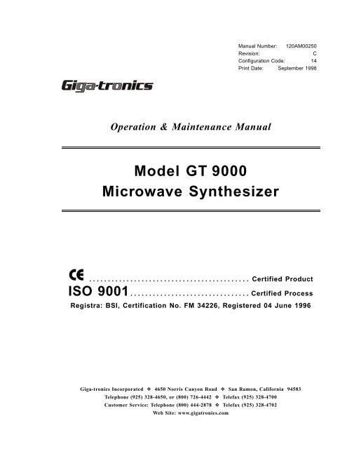
<strong>Manual</strong> Number: 120AM00250<br />
Revision:<br />
C<br />
Configuration Code: 14<br />
Print Date: September 1998<br />
Operation & Maintenance <strong>Manual</strong><br />
Model GT 9000<br />
Microwave Synthesizer<br />
. . . . . . . . . . . . . . . . . . . . . . . . . . . . . . . . . . . . . . . . . . . Certified Product<br />
ISO 9001 . . . . . . . . . . . . . . . . . . . . . . . . . . . . . . . . Certified Process<br />
Registra: BSI, Certification No. FM 34226, Registered 04 June 1996<br />
Giga-tronics Incorporated ❖ 4650 Norris Canyon Road ❖ San Ramon, California 94583<br />
Telephone (925) 328-4650, or (800) 726-4442 ❖ Telefax (925) 328-4700<br />
Customer Service: Telephone (800) 444-2878 ❖ Telefax (925) 328-4702<br />
Web Site: www.gigatronics.com
All technical data and specifications in this manual are subject to change without prior notice and<br />
do not represent a commitment on the part of Giga-tronics Incorporated.<br />
© Copyright Giga-tronics Incorporated 1998. All rights reserved.<br />
Printed in U.S.A.<br />
WARRANTY<br />
Giga-tronics products are warranted against defective materials and<br />
workmanship for one year from date of shipment. Giga-tronics will at its<br />
option repair or replace products that are proven defective during the<br />
warranty period. This warranty DOES NOT cover damage resulting from<br />
improper use, nor workmanship other than Giga-tronics service. There is<br />
no implied warranty of fitness for a particular purpose, nor is<br />
Giga-tronics liable for any consequential damages. Specification and<br />
price change privileges are reserved by Giga-tronics.<br />
Giga-tronics Service Contacts<br />
Territory Primary Contact Secondary Contact<br />
Customer Service: USA & Canada (800) 444-2878<br />
(925) 328-4646<br />
Pacific Rim & Far East (800) 444-2878<br />
(925) 328-4646<br />
Europe & South Africa (800) 444-2878<br />
(925) 328-4646<br />
(800) 726-4442<br />
(925) 328-4660<br />
(800) 726-4442<br />
(925) 328-4670<br />
(800) 726-4442<br />
(925) 328-4664<br />
Applications and Technical<br />
Support:<br />
All Territories (800) 726-4142<br />
(925) 328-4665<br />
(800) 726-4442<br />
(925) 328-4669
Table of Contents<br />
About This <strong>Manual</strong> . . . . . . . . . . . . . . . . . . . . . . . . . . . . . . . . . . . . . . . . . . . . . .<br />
Conventions. . . . . . . . . . . . . . . . . . . . . . . . . . . . . . . . . . . . . . . . . . . . . . . . . . . .<br />
Record of <strong>Manual</strong> Changes . . . . . . . . . . . . . . . . . . . . . . . . . . . . . . . . . . . . . . .<br />
Special Configurations . . . . . . . . . . . . . . . . . . . . . . . . . . . . . . . . . . . . . . . . . . .<br />
xi<br />
xiii<br />
xv<br />
xvii<br />
1 • Introduction _______________________________________________________<br />
1.1 General Information. . . . . . . . . . . . . . . . . . . . . . . . . . . . . . . . . . . . . . . . . . . . . . . . . . . . . . . . 1-1<br />
1.1.1 Introduction. . . . . . . . . . . . . . . . . . . . . . . . . . . . . . . . . . . . . . . . . . . . . . . . . . . . . . . . 1-1<br />
1.1.2 Items Furnished . . . . . . . . . . . . . . . . . . . . . . . . . . . . . . . . . . . . . . . . . . . . . . . . . . . . 1-2<br />
1.1.3 Items Required. . . . . . . . . . . . . . . . . . . . . . . . . . . . . . . . . . . . . . . . . . . . . . . . . . . . . 1-2<br />
1.1.4 Tools and Test Equipment . . . . . . . . . . . . . . . . . . . . . . . . . . . . . . . . . . . . . . . . . . . 1-2<br />
1.1.5 Cooling . . . . . . . . . . . . . . . . . . . . . . . . . . . . . . . . . . . . . . . . . . . . . . . . . . . . . . . . . . . 1-2<br />
1.1.6 Cleaning . . . . . . . . . . . . . . . . . . . . . . . . . . . . . . . . . . . . . . . . . . . . . . . . . . . . . . . . . . 1-2<br />
1.1.7 Installation and Preparation for Use . . . . . . . . . . . . . . . . . . . . . . . . . . . . . . . . . . . . 1-2<br />
1.1.8 Receiving Inspection . . . . . . . . . . . . . . . . . . . . . . . . . . . . . . . . . . . . . . . . . . . . . . . . 1-2<br />
1.1.9 Preparation for Reshipment. . . . . . . . . . . . . . . . . . . . . . . . . . . . . . . . . . . . . . . . . . . 1-3<br />
1.2 Safety Precautions . . . . . . . . . . . . . . . . . . . . . . . . . . . . . . . . . . . . . . . . . . . . . . . . . . . . . . . . 1-4<br />
1.2.1 Voltage and Fuse Selection . . . . . . . . . . . . . . . . . . . . . . . . . . . . . . . . . . . . . . . . . . 1-5<br />
1.3 Performance Specifications. . . . . . . . . . . . . . . . . . . . . . . . . . . . . . . . . . . . . . . . . . . . . . . . . . 1-6<br />
1.3.1 CW Operation . . . . . . . . . . . . . . . . . . . . . . . . . . . . . . . . . . . . . . . . . . . . . . . . . . . . . 1-6<br />
1.3.2 Spectral Purity . . . . . . . . . . . . . . . . . . . . . . . . . . . . . . . . . . . . . . . . . . . . . . . . . . . . . 1-6<br />
1.3.3 RF Output Power . . . . . . . . . . . . . . . . . . . . . . . . . . . . . . . . . . . . . . . . . . . . . . . . . . . 1-7<br />
1.3.4 PM Envelope Parameters . . . . . . . . . . . . . . . . . . . . . . . . . . . . . . . . . . . . . . . . . . . . 1-7<br />
1.3.5 Internally Generated PM Repetition Rate . . . . . . . . . . . . . . . . . . . . . . . . . . . . . . . . 1-8<br />
1.3.6 Internally Generated PM Delay . . . . . . . . . . . . . . . . . . . . . . . . . . . . . . . . . . . . . . . . 1-8<br />
1.3.7 Internally Generated PM Width . . . . . . . . . . . . . . . . . . . . . . . . . . . . . . . . . . . . . . . . 1-8<br />
1.3.8 Externally Triggered PM Envelope . . . . . . . . . . . . . . . . . . . . . . . . . . . . . . . . . . . . . 1-8<br />
1.3.9 Externally Generated PM Envelope . . . . . . . . . . . . . . . . . . . . . . . . . . . . . . . . . . . . 1-8<br />
1.3.10 FM Envelope Parameters (Wide or Narrow Mode) . . . . . . . . . . . . . . . . . . . . . . . . 1-9<br />
1.3.11 FM Envelope Parameters (Wide Mode) . . . . . . . . . . . . . . . . . . . . . . . . . . . . . . . . . 1-9<br />
1.3.12 FM Envelope Parameters (Narrow Mode) . . . . . . . . . . . . . . . . . . . . . . . . . . . . . . . 1-9<br />
1.3.13 FM Indicator . . . . . . . . . . . . . . . . . . . . . . . . . . . . . . . . . . . . . . . . . . . . . . . . . . . . . . . 1-9<br />
1.3.14 Internally Generated FM Envelope (Option 24 only) . . . . . . . . . . . . . . . . . . . . . . . 1-9<br />
1.3.15 Externally Supplied FM Envelope . . . . . . . . . . . . . . . . . . . . . . . . . . . . . . . . . . . . . . 1-10<br />
1.3.16 Amplitude Modulation . . . . . . . . . . . . . . . . . . . . . . . . . . . . . . . . . . . . . . . . . . . . . . . 1-10<br />
1.3.17 AM Indicator . . . . . . . . . . . . . . . . . . . . . . . . . . . . . . . . . . . . . . . . . . . . . . . . . . . . . . . 1-10<br />
1.3.18 Internally Generated AM Envelope . . . . . . . . . . . . . . . . . . . . . . . . . . . . . . . . . . . . . 1-10<br />
1.3.19 Externally Supplied AM Envelope . . . . . . . . . . . . . . . . . . . . . . . . . . . . . . . . . . . . . . 1-11<br />
1.3.20 External Automatic Level Control . . . . . . . . . . . . . . . . . . . . . . . . . . . . . . . . . . . . . . 1-11<br />
1.3.21 Front Panel Inputs/Outputs . . . . . . . . . . . . . . . . . . . . . . . . . . . . . . . . . . . . . . . . . . . 1-11<br />
1.3.22 Rear Panel Inputs/Outputs . . . . . . . . . . . . . . . . . . . . . . . . . . . . . . . . . . . . . . . . . . . 1-11<br />
1.3.23 General Specifications . . . . . . . . . . . . . . . . . . . . . . . . . . . . . . . . . . . . . . . . . . . . . . . 1-12<br />
2 • Operation _________________________________________________________<br />
2.1 Introduction . . . . . . . . . . . . . . . . . . . . . . . . . . . . . . . . . . . . . . . . . . . . . . . . . . . . . . . . . . . . . . 2-1<br />
2.2 The Front Panel. . . . . . . . . . . . . . . . . . . . . . . . . . . . . . . . . . . . . . . . . . . . . . . . . . . . . . . . . . . 2-1<br />
<strong>Manual</strong> No. 120AM00250, Rev C, September 1998<br />
i
Series GT 9000 Microwave Synthesizers<br />
2.2.1 Entry Menu . . . . . . . . . . . . . . . . . . . . . . . . . . . . . . . . . . . . . . . . . . . . . . . . . . . . . . . . 2-2<br />
2.2.2 Data Entry Field . . . . . . . . . . . . . . . . . . . . . . . . . . . . . . . . . . . . . . . . . . . . . . . . . . . . 2-3<br />
2.2.3 Shifted Functions . . . . . . . . . . . . . . . . . . . . . . . . . . . . . . . . . . . . . . . . . . . . . . . . . . . 2-5<br />
2.2.4 Frequency . . . . . . . . . . . . . . . . . . . . . . . . . . . . . . . . . . . . . . . . . . . . . . . . . . . . . . . . . 2-8<br />
2.2.5 RF Level . . . . . . . . . . . . . . . . . . . . . . . . . . . . . . . . . . . . . . . . . . . . . . . . . . . . . . . . . . 2-9<br />
2.2.6 Pulse Modulation . . . . . . . . . . . . . . . . . . . . . . . . . . . . . . . . . . . . . . . . . . . . . . . . . . . 2-10<br />
2.2.7 Frequency Modulation . . . . . . . . . . . . . . . . . . . . . . . . . . . . . . . . . . . . . . . . . . . . . . . 2-12<br />
2.2.8 Amplitude Modulation . . . . . . . . . . . . . . . . . . . . . . . . . . . . . . . . . . . . . . . . . . . . . . . . 2-14<br />
2.3 The Rear Panel . . . . . . . . . . . . . . . . . . . . . . . . . . . . . . . . . . . . . . . . . . . . . . . . . . . . . . . . . . . 2-16<br />
2.3.1 BNCs . . . . . . . . . . . . . . . . . . . . . . . . . . . . . . . . . . . . . . . . . . . . . . . . . . . . . . . . . . . . . 2-16<br />
2.3.2 Line Power and Fuse . . . . . . . . . . . . . . . . . . . . . . . . . . . . . . . . . . . . . . . . . . . . . . . . 2-17<br />
2.3.3 IEEE-488 Interface . . . . . . . . . . . . . . . . . . . . . . . . . . . . . . . . . . . . . . . . . . . . . . . . . . 2-17<br />
2.4 GT 9000 Syntax . . . . . . . . . . . . . . . . . . . . . . . . . . . . . . . . . . . . . . . . . . . . . . . . . . . . . . . . . . . 2-19<br />
2.4.1 GT 9000 Syntax Virtual Keystrokes. . . . . . . . . . . . . . . . . . . . . . . . . . . . . . . . . . . . . 2-24<br />
2.5 1026 Syntax Interface . . . . . . . . . . . . . . . . . . . . . . . . . . . . . . . . . . . . . . . . . . . . . . . . . . . . . . 2-25<br />
2.5.1 Character Representation . . . . . . . . . . . . . . . . . . . . . . . . . . . . . . . . . . . . . . . . . . . . 2-25<br />
2.5.2 Command Format . . . . . . . . . . . . . . . . . . . . . . . . . . . . . . . . . . . . . . . . . . . . . . . . . . . 2-25<br />
2.5.3 Commands . . . . . . . . . . . . . . . . . . . . . . . . . . . . . . . . . . . . . . . . . . . . . . . . . . . . . . . . 2-26<br />
3 • Theory of Operation ________________________________________________<br />
3.1 Introduction . . . . . . . . . . . . . . . . . . . . . . . . . . . . . . . . . . . . . . . . . . . . . . . . . . . . . . . . . . . . . . . 3-1<br />
3.2 General Circuit Theory. . . . . . . . . . . . . . . . . . . . . . . . . . . . . . . . . . . . . . . . . . . . . . . . . . . . . . 3-1<br />
3.2.1 The Computer . . . . . . . . . . . . . . . . . . . . . . . . . . . . . . . . . . . . . . . . . . . . . . . . . . . . . . 3-2<br />
3.2.2 The RF Path . . . . . . . . . . . . . . . . . . . . . . . . . . . . . . . . . . . . . . . . . . . . . . . . . . . . . . . 3-3<br />
3.2.3 Phase Lock Loops . . . . . . . . . . . . . . . . . . . . . . . . . . . . . . . . . . . . . . . . . . . . . . . . . . 3-3<br />
3.2.4 Dual-Loop Indirect Synthesis . . . . . . . . . . . . . . . . . . . . . . . . . . . . . . . . . . . . . . . . . . 3-5<br />
3.2.5 The Output Loop. . . . . . . . . . . . . . . . . . . . . . . . . . . . . . . . . . . . . . . . . . . . . . . . . . . . 3-6<br />
3.2.6 The Reference Loop. . . . . . . . . . . . . . . . . . . . . . . . . . . . . . . . . . . . . . . . . . . . . . . . . 3-8<br />
3.2.7 The Downconverter . . . . . . . . . . . . . . . . . . . . . . . . . . . . . . . . . . . . . . . . . . . . . . . . . 3-12<br />
3.2.8 Level Control. . . . . . . . . . . . . . . . . . . . . . . . . . . . . . . . . . . . . . . . . . . . . . . . . . . . . . . 3-15<br />
3.2.9 Frequency Modulation . . . . . . . . . . . . . . . . . . . . . . . . . . . . . . . . . . . . . . . . . . . . . . . 3-17<br />
3.2.10 Amplitude Modulation . . . . . . . . . . . . . . . . . . . . . . . . . . . . . . . . . . . . . . . . . . . . . . . . 3-17<br />
3.2.11 Pulse Modulation . . . . . . . . . . . . . . . . . . . . . . . . . . . . . . . . . . . . . . . . . . . . . . . . . . . 3-17<br />
3.3 Assembly Circuit Descriptions . . . . . . . . . . . . . . . . . . . . . . . . . . . . . . . . . . . . . . . . . . . . . . . . 3-18<br />
3.3.1 Front Panel Interface — PC Assembly A1 . . . . . . . . . . . . . . . . . . . . . . . . . . . . . . . 3-18<br />
3.3.2 IEEE / TIMER — PC Assembly A2 . . . . . . . . . . . . . . . . . . . . . . . . . . . . . . . . . . . . . 3-18<br />
3.3.3 Memory — PC Assembly A3 . . . . . . . . . . . . . . . . . . . . . . . . . . . . . . . . . . . . . . . . . . 3-19<br />
3.3.4 CPU — PC Assembly A4 . . . . . . . . . . . . . . . . . . . . . . . . . . . . . . . . . . . . . . . . . . . . . 3-20<br />
3.3.5 Pulse Driver — PC Assembly A5. . . . . . . . . . . . . . . . . . . . . . . . . . . . . . . . . . . . . . . 3-20<br />
3.3.6 Pulse Generator — PC Assembly A5A1 . . . . . . . . . . . . . . . . . . . . . . . . . . . . . . . . . 3-21<br />
3.3.7 AM/FM Driver — PC Assembly A6 . . . . . . . . . . . . . . . . . . . . . . . . . . . . . . . . . . . . . 3-21<br />
3.3.8 Function Generator — PC Assembly A6A1. . . . . . . . . . . . . . . . . . . . . . . . . . . . . . . 3-22<br />
3.3.9 Scan Modulation — PC Assembly A7 . . . . . . . . . . . . . . . . . . . . . . . . . . . . . . . . . . . 3-22<br />
3.3.10 Level — PC Assembly A10 . . . . . . . . . . . . . . . . . . . . . . . . . . . . . . . . . . . . . . . . . . . 3-23<br />
3.3.11 Level Driver — PC Assembly A10A1 . . . . . . . . . . . . . . . . . . . . . . . . . . . . . . . . . . . 3-24<br />
3.3.12 Power Supply — PC Assembly A11 . . . . . . . . . . . . . . . . . . . . . . . . . . . . . . . . . . . . 3-25<br />
3.3.13 100 MHz Reference PLL — PC Assembly A14 . . . . . . . . . . . . . . . . . . . . . . . . . . . 3-26<br />
3.3.14 1 Hz PLL — PC Assembly A15 . . . . . . . . . . . . . . . . . . . . . . . . . . . . . . . . . . . . . . . . 3-27<br />
3.3.15 Reference / Downconverter PLL — PC Assembly A16 . . . . . . . . . . . . . . . . . . . . . 3-28<br />
3.3.16 Divide-By-N — PC Assembly A17 . . . . . . . . . . . . . . . . . . . . . . . . . . . . . . . . . . . . . . 3-30<br />
3.3.17 Output PLL — PC Assembly A18 . . . . . . . . . . . . . . . . . . . . . . . . . . . . . . . . . . . . . . 3-32<br />
3.3.18 YIG Driver — PC Assembly A19 . . . . . . . . . . . . . . . . . . . . . . . . . . . . . . . . . . . . . . . 3-33<br />
3.3.19 Display Driver — PC Assembly A20 . . . . . . . . . . . . . . . . . . . . . . . . . . . . . . . . . . . . 3-33<br />
ii <strong>Manual</strong> No. 120AM00250, Rev C, September 1998
Preface<br />
3.3.20 Pushbutton — PC Assembly A105 . . . . . . . . . . . . . . . . . . . . . . . . . . . . . . . . . . . . . 3-33<br />
3.3.21 Data Entry — PC Assembly A106 . . . . . . . . . . . . . . . . . . . . . . . . . . . . . . . . . . . . . 3-34<br />
3.3.22 Main Tune — PC Assembly A107 . . . . . . . . . . . . . . . . . . . . . . . . . . . . . . . . . . . . . 3-34<br />
3.3.23 Detector Buffer — PC Assembly A200 . . . . . . . . . . . . . . . . . . . . . . . . . . . . . . . . . . 3-34<br />
3.3.24 100 MHz Oscillator/Sampler Driver — PC Assembly A201 . . . . . . . . . . . . . . . . . . 3-35<br />
4 • Calibration and Testing _____________________________________________<br />
4.1 Calibration Procedures . . . . . . . . . . . . . . . . . . . . . . . . . . . . . . . . . . . . . . . . . . . . . . . . . . . . . 4-1<br />
4.1.1 Recommended Equipment: . . . . . . . . . . . . . . . . . . . . . . . . . . . . . . . . . . . . . . . . . . . 4-1<br />
4.1.2 Power Supply Calibration . . . . . . . . . . . . . . . . . . . . . . . . . . . . . . . . . . . . . . . . . . . . 4-2<br />
4.1.3 100 MHz Phase Lock Loop . . . . . . . . . . . . . . . . . . . . . . . . . . . . . . . . . . . . . . . . . . . 4-3<br />
4.1.4 Sampler Drivers, 100 MHz VCO (Optional) . . . . . . . . . . . . . . . . . . . . . . . . . . . . . . 4-3<br />
4.1.5 YIG Driver Calibration . . . . . . . . . . . . . . . . . . . . . . . . . . . . . . . . . . . . . . . . . . . . . . . 4-4<br />
4.1.6 Level Calibration . . . . . . . . . . . . . . . . . . . . . . . . . . . . . . . . . . . . . . . . . . . . . . . . . . . 4-5<br />
4.1.7 AM/FM Generator Verification (Option 24 only) . . . . . . . . . . . . . . . . . . . . . . . . . . . 4-6<br />
4.1.8 Pulse Generator Verification . . . . . . . . . . . . . . . . . . . . . . . . . . . . . . . . . . . . . . . . . 4-7<br />
4.1.9 AM Calibration . . . . . . . . . . . . . . . . . . . . . . . . . . . . . . . . . . . . . . . . . . . . . . . . . . . . . 4-8<br />
4.1.10 FM Calibration . . . . . . . . . . . . . . . . . . . . . . . . . . . . . . . . . . . . . . . . . . . . . . . . . . . . . 4-9<br />
4.1.11 Spectral Purity . . . . . . . . . . . . . . . . . . . . . . . . . . . . . . . . . . . . . . . . . . . . . . . . . . . . . 4-10<br />
4.1.12 10 MHz Time Base . . . . . . . . . . . . . . . . . . . . . . . . . . . . . . . . . . . . . . . . . . . . . . . . . 4-10<br />
4.2 Performance Tests . . . . . . . . . . . . . . . . . . . . . . . . . . . . . . . . . . . . . . . . . . . . . . . . . . . . . . . . 4-11<br />
4.2.1 Equipment Required . . . . . . . . . . . . . . . . . . . . . . . . . . . . . . . . . . . . . . . . . . . . . . . . 4-11<br />
4.2.2 Test Data Sheet. . . . . . . . . . . . . . . . . . . . . . . . . . . . . . . . . . . . . . . . . . . . . . . . . . . . 4-11<br />
4.2.3 Calibration Cycle . . . . . . . . . . . . . . . . . . . . . . . . . . . . . . . . . . . . . . . . . . . . . . . . . . . 4-11<br />
4.2.4 Warm-up. . . . . . . . . . . . . . . . . . . . . . . . . . . . . . . . . . . . . . . . . . . . . . . . . . . . . . . . . . 4-11<br />
4.2.5 Frequency Range, Resolution and Accuracy . . . . . . . . . . . . . . . . . . . . . . . . . . . . . 4-12<br />
4.2.6 Spurious Signals Tests . . . . . . . . . . . . . . . . . . . . . . . . . . . . . . . . . . . . . . . . . . . . . . 4-14<br />
4.2.7 Single Sideband Phase Noise. . . . . . . . . . . . . . . . . . . . . . . . . . . . . . . . . . . . . . . . . 4-16<br />
4.2.8 RF Output Power Tests. . . . . . . . . . . . . . . . . . . . . . . . . . . . . . . . . . . . . . . . . . . . . . 4-17<br />
4.2.9 Pulse Modulation On/Off Ratio Test . . . . . . . . . . . . . . . . . . . . . . . . . . . . . . . . . . . . 4-19<br />
4.2.10 Pulse Modulation Rise and Fall Time Test. . . . . . . . . . . . . . . . . . . . . . . . . . . . . . . 4-20<br />
4.2.11 Pulse Modulation Overshoot and Settling Time . . . . . . . . . . . . . . . . . . . . . . . . . . . 4-21<br />
4.2.12 Pulse Modulation Accuracy Test . . . . . . . . . . . . . . . . . . . . . . . . . . . . . . . . . . . . . . . 4-23<br />
4.2.13 Internal Pulse Generator Tests . . . . . . . . . . . . . . . . . . . . . . . . . . . . . . . . . . . . . . . . 4-24<br />
4.2.14 Frequency Modulation Tests . . . . . . . . . . . . . . . . . . . . . . . . . . . . . . . . . . . . . . . . . . 4-25<br />
4.2.15 Internal Modulation Generator Tests (Option 24 Only) . . . . . . . . . . . . . . . . . . . . . 4-27<br />
5 • Maintenance ______________________________________________________<br />
5.1 Introduction . . . . . . . . . . . . . . . . . . . . . . . . . . . . . . . . . . . . . . . . . . . . . . . . . . . . . . . . . . . . . . 5-1<br />
5.2 Malfunctions. . . . . . . . . . . . . . . . . . . . . . . . . . . . . . . . . . . . . . . . . . . . . . . . . . . . . . . . . . . . . . 5-2<br />
5.2.1 General Failure . . . . . . . . . . . . . . . . . . . . . . . . . . . . . . . . . . . . . . . . . . . . . . . . . . . . 5-2<br />
5.2.2 Loss of RF Output . . . . . . . . . . . . . . . . . . . . . . . . . . . . . . . . . . . . . . . . . . . . . . . . . . 5-2<br />
5.2.3 Incorrect Output Level . . . . . . . . . . . . . . . . . . . . . . . . . . . . . . . . . . . . . . . . . . . . . . . 5-2<br />
5.2.4 Output Frequency Unlocked . . . . . . . . . . . . . . . . . . . . . . . . . . . . . . . . . . . . . . . . . . 5-4<br />
5.2.5 Output Locked, but Frequency Incorrect . . . . . . . . . . . . . . . . . . . . . . . . . . . . . . . . 5-5<br />
5.2.6 IEEE-488 Interface Malfunction. . . . . . . . . . . . . . . . . . . . . . . . . . . . . . . . . . . . . . . . 5-5<br />
5.3 Troubleshooting Notes . . . . . . . . . . . . . . . . . . . . . . . . . . . . . . . . . . . . . . . . . . . . . . . . . . . . . 5-6<br />
5.3.1 Power Supply . . . . . . . . . . . . . . . . . . . . . . . . . . . . . . . . . . . . . . . . . . . . . . . . . . . . . . 5-6<br />
5.3.2 The Computer . . . . . . . . . . . . . . . . . . . . . . . . . . . . . . . . . . . . . . . . . . . . . . . . . . . . . 5-8<br />
5.3.3 10 dB Step Attenuator (Option 26) . . . . . . . . . . . . . . . . . . . . . . . . . . . . . . . . . . . . . 5-8<br />
5.3.4 YIG Oscillator . . . . . . . . . . . . . . . . . . . . . . . . . . . . . . . . . . . . . . . . . . . . . . . . . . . . . . 5-9<br />
5.3.5 Microwave Module . . . . . . . . . . . . . . . . . . . . . . . . . . . . . . . . . . . . . . . . . . . . . . . . . . 5-9<br />
5.3.6 Detector . . . . . . . . . . . . . . . . . . . . . . . . . . . . . . . . . . . . . . . . . . . . . . . . . . . . . . . . . . 5-10<br />
<strong>Manual</strong> No. 120AM00250, Rev C, September 1998<br />
iii
Series GT 9000 Microwave Synthesizers<br />
5.3.7 Level Control Circuit . . . . . . . . . . . . . . . . . . . . . . . . . . . . . . . . . . . . . . . . . . . . . . . . . 5-11<br />
5.3.8 Output Phase Lock Loop . . . . . . . . . . . . . . . . . . . . . . . . . . . . . . . . . . . . . . . . . . . . . 5-12<br />
5.3.9 Divide-By-N . . . . . . . . . . . . . . . . . . . . . . . . . . . . . . . . . . . . . . . . . . . . . . . . . . . . . . . . 5-12<br />
5.3.10 YIG Driver . . . . . . . . . . . . . . . . . . . . . . . . . . . . . . . . . . . . . . . . . . . . . . . . . . . . . . . . . 5-13<br />
5.3.11 100 MHz Module . . . . . . . . . . . . . . . . . . . . . . . . . . . . . . . . . . . . . . . . . . . . . . . . . . . 5-13<br />
5.3.12 100 MHz PLL . . . . . . . . . . . . . . . . . . . . . . . . . . . . . . . . . . . . . . . . . . . . . . . . . . . . . . 5-14<br />
5.3.13 10 MHz Master Reference . . . . . . . . . . . . . . . . . . . . . . . . . . . . . . . . . . . . . . . . . . . . 5-14<br />
5.3.14 1 Hz PLL . . . . . . . . . . . . . . . . . . . . . . . . . . . . . . . . . . . . . . . . . . . . . . . . . . . . . . . . . . 5-14<br />
5.3.15 IEEE-488 Interface/Timer Circuit . . . . . . . . . . . . . . . . . . . . . . . . . . . . . . . . . . . . . . . 5-14<br />
5.3.16 Downconverter PLL . . . . . . . . . . . . . . . . . . . . . . . . . . . . . . . . . . . . . . . . . . . . . . . . . 5-14<br />
5.3.17 Reference Mixer . . . . . . . . . . . . . . . . . . . . . . . . . . . . . . . . . . . . . . . . . . . . . . . . . . . . 5-15<br />
5.3.18 Reference PLL . . . . . . . . . . . . . . . . . . . . . . . . . . . . . . . . . . . . . . . . . . . . . . . . . . . . . 5-15<br />
6 • Parts Lists ________________________________________________________<br />
6.1 Introduction . . . . . . . . . . . . . . . . . . . . . . . . . . . . . . . . . . . . . . . . . . . . . . . . . . . . . . . . . . . . . . . 6-1<br />
<strong>GT9000</strong>/.01-20 MICROWAVE SIGNAL GENERATOR. . . . . . . . . . . . . . . . . . . . . . . . . . . . . 6-1<br />
<strong>GT9000</strong>/.5-20 MICROWAVE SIGNAL GENERATOR. . . . . . . . . . . . . . . . . . . . . . . . . . . . . . 6-1<br />
<strong>GT9000</strong>/2-20 MICROWAVE SIGNAL GENERATOR . . . . . . . . . . . . . . . . . . . . . . . . . . . . . . 6-2<br />
<strong>GT9000</strong>/.01-26 MICROWAVE SIGNAL GENERATOR. . . . . . . . . . . . . . . . . . . . . . . . . . . . . 6-2<br />
<strong>GT9000</strong>/.5-26 MICROWAVE SIGNAL GENERATOR. . . . . . . . . . . . . . . . . . . . . . . . . . . . . . 6-2<br />
<strong>GT9000</strong>/2-26 MICROWAVE SIGNAL GENERATOR . . . . . . . . . . . . . . . . . . . . . . . . . . . . . . 6-2<br />
120DA00952 <strong>GT9000</strong> CHASSIS W/ SW PS . . . . . . . . . . . . . . . . . . . . . . . . . . . . . . . . . . . . 6-3<br />
120DA11052 <strong>GT9000</strong> R/P ASY FOR SW PS . . . . . . . . . . . . . . . . . . . . . . . . . . . . . . . . . . . 6-4<br />
1204206652 <strong>GT9000</strong> FRONT PANEL ASY . . . . . . . . . . . . . . . . . . . . . . . . . . . . . . . . . . . . . 6-4<br />
120CA16450 <strong>GT9000</strong>/S FRONT PANEL OUT . . . . . . . . . . . . . . . . . . . . . . . . . . . . . . . . . . . 6-5<br />
120DA00750 <strong>GT9000</strong> PCB ASSY SET . . . . . . . . . . . . . . . . . . . . . . . . . . . . . . . . . . . . . . . . 6-5<br />
420BA48600 LEVEL ASY;<strong>GT9000</strong> . . . . . . . . . . . . . . . . . . . . . . . . . . . . . . . . . . . . . . . . . . . . 6-5<br />
120DA00501 .01-26 GHZ FREQ ASSY . . . . . . . . . . . . . . . . . . . . . . . . . . . . . . . . . . . . . . . . 6-6<br />
120DA00500 .01-20 GHZ FREQ. ASSY . . . . . . . . . . . . . . . . . . . . . . . . . . . . . . . . . . . . . . . . 6-6<br />
120DA00510 .5-20 GHZ FREQ. ASSY . . . . . . . . . . . . . . . . . . . . . . . . . . . . . . . . . . . . . . . . . 6-7<br />
120DA00511 .5-26 GHZ FREQ ASSY . . . . . . . . . . . . . . . . . . . . . . . . . . . . . . . . . . . . . . . . . 6-7<br />
120DA00520 2-20 GHZ FREQ ASSY . . . . . . . . . . . . . . . . . . . . . . . . . . . . . . . . . . . . . . . . . . 6-8<br />
120DA00521 2-26 GHZ FREQ ASSY . . . . . . . . . . . . . . . . . . . . . . . . . . . . . . . . . . . . . . . . . . 6-8<br />
420DA46900 <strong>GT9000</strong> STD MICROWAVE DEC . . . . . . . . . . . . . . . . . . . . . . . . . . . . . . . . . . 6-9<br />
420CA46800 100 MHZ MT ASY;2SAMP;GT9 . . . . . . . . . . . . . . . . . . . . . . . . . . . . . . . . . . . 6-9<br />
004BA00001 SAMPLER ASSEMBLY . . . . . . . . . . . . . . . . . . . . . . . . . . . . . . . . . . . . . . . . . . 6-9<br />
004BA00101 SAMPLER ASSY REVERSE MTG . . . . . . . . . . . . . . . . . . . . . . . . . . . . . . . . . 6-9<br />
30413 .01-26.5 GHz SUBASSY . . . . . . . . . . . . . . . . . . . . . . . . . . . . . . . . . . . . . . . . . . . . . . 6-10<br />
004BA34700 <strong>GT9000</strong>/S .01-2 DOWNC ASY . . . . . . . . . . . . . . . . . . . . . . . . . . . . . . . . . . . . 6-13<br />
004BA34600 <strong>GT9000</strong>/S .01-2 FILTER AS . . . . . . . . . . . . . . . . . . . . . . . . . . . . . . . . . . . . . . 6-13<br />
004BA34800 <strong>GT9000</strong>/S .5-2 FILTER ASY . . . . . . . . . . . . . . . . . . . . . . . . . . . . . . . . . . . . . . 6-13<br />
120DA11250 <strong>GT9000</strong> BENCH MT DRESS . . . . . . . . . . . . . . . . . . . . . . . . . . . . . . . . . . . . . 6-14<br />
120DA04550 BOTTOM COVER ASY . . . . . . . . . . . . . . . . . . . . . . . . . . . . . . . . . . . . . . . . . . 6-14<br />
120AA14300 ACCESSORIES ASY . . . . . . . . . . . . . . . . . . . . . . . . . . . . . . . . . . . . . . . . . . . . 6-14<br />
120BA01300 FRONT PANEL I/F PCA (A1) . . . . . . . . . . . . . . . . . . . . . . . . . . . . . . . . . . . . . 6-15<br />
120BA05300 IEEE / TIMER PCA (A2) . . . . . . . . . . . . . . . . . . . . . . . . . . . . . . . . . . . . . . . . . 6-16<br />
120BA01200 MEMORY PCA (A3). . . . . . . . . . . . . . . . . . . . . . . . . . . . . . . . . . . . . . . . . . . . . 6-17<br />
120BA01100 CPU PCA (A4) . . . . . . . . . . . . . . . . . . . . . . . . . . . . . . . . . . . . . . . . . . . . . . . . . 6-18<br />
120BA09303 PULSE DRIVER PCA (A5) . . . . . . . . . . . . . . . . . . . . . . . . . . . . . . . . . . . . . . . 6-19<br />
120BA12550 <strong>GT9000</strong> PULSE GENERATOR (A5A1). . . . . . . . . . . . . . . . . . . . . . . . . . . . . . 6-21<br />
120BA09401 AM/FM DRIVER PCA (A6) . . . . . . . . . . . . . . . . . . . . . . . . . . . . . . . . . . . . . . . 6-23<br />
420BA47500 <strong>GT9000</strong> LEVEL PCA (A10) . . . . . . . . . . . . . . . . . . . . . . . . . . . . . . . . . . . . . . . 6-26<br />
420BA50500 LEVEL DRIVER AM 9000 PCA (A10A1) . . . . . . . . . . . . . . . . . . . . . . . . . . . . 6-29<br />
iv <strong>Manual</strong> No. 120AM00250, Rev C, September 1998
Preface<br />
120BA04650 POWER SUPPLY PCA (A11). . . . . . . . . . . . . . . . . . . . . . . . . . . . . . . . . . . . . 6-31<br />
120BA06951 100 MHz PLL PCA (A14) . . . . . . . . . . . . . . . . . . . . . . . . . . . . . . . . . . . . . . . . 6-32<br />
120BA08800 1 HZ PLL PCA (A15) . . . . . . . . . . . . . . . . . . . . . . . . . . . . . . . . . . . . . . . . . . . 6-35<br />
120BA07000 REF/DC PLL PCA (A16). . . . . . . . . . . . . . . . . . . . . . . . . . . . . . . . . . . . . . . . . 6-38<br />
120BA07150 DIVIDE BY N PCA (A17) . . . . . . . . . . . . . . . . . . . . . . . . . . . . . . . . . . . . . . . . 6-41<br />
120BA07250 OUTPUT PLL PCA (A18) . . . . . . . . . . . . . . . . . . . . . . . . . . . . . . . . . . . . . . . . 6-43<br />
120BA08350 YIG DRIVER PCA (A19). . . . . . . . . . . . . . . . . . . . . . . . . . . . . . . . . . . . . . . . . 6-46<br />
1202221000 <strong>GT9000</strong> DISP DRIVER PCA (A20) . . . . . . . . . . . . . . . . . . . . . . . . . . . . . . . . . 6-48<br />
101BA39101 HI STAB OSC PCA (A21). . . . . . . . . . . . . . . . . . . . . . . . . . . . . . . . . . . . . . . . 6-49<br />
120BA01000 COMPUTER BUS PCA (A100). . . . . . . . . . . . . . . . . . . . . . . . . . . . . . . . . . . . 6-49<br />
120BA07300 I/O BUSS PCA (A101) . . . . . . . . . . . . . . . . . . . . . . . . . . . . . . . . . . . . . . . . . . 6-49<br />
120BA05520 11 DIGIT DISPLY PCA NVFD (A103) . . . . . . . . . . . . . . . . . . . . . . . . . . . . . . 6-49<br />
120BA05621 5 DIGIT DISPLAY PCA NVFD (A104) . . . . . . . . . . . . . . . . . . . . . . . . . . . . . . 6-50<br />
120BA04850 PUSHBUTTON PCA (A105) . . . . . . . . . . . . . . . . . . . . . . . . . . . . . . . . . . . . . . 6-50<br />
120BA01512 DATA ENTRY M7100 PCA (A106) . . . . . . . . . . . . . . . . . . . . . . . . . . . . . . . . 6-50<br />
120BA12900 MAIN TUNE PCA (A107)1 . . . . . . . . . . . . . . . . . . . . . . . . . . . . . . . . . . . . . . . 6-51<br />
120BA07900 DETECTOR BUFFER PCA (A200) . . . . . . . . . . . . . . . . . . . . . . . . . . . . . . . . 6-52<br />
120CA11502 100MHZ MODULE ASY (A201); <strong>GT9000</strong> . . . . . . . . . . . . . . . . . . . . . . . . . . . 6-53<br />
101CA04203 100 MHz MODULE PCA; <strong>GT9000</strong> . . . . . . . . . . . . . . . . . . . . . . . . . . . . . . . . . 6-54<br />
6.2 List of Manufacturers. . . . . . . . . . . . . . . . . . . . . . . . . . . . . . . . . . . . . . . . . . . . . . . . . . . . . . . 6-57<br />
7 • Diagrams _________________________________________________________<br />
7.1 Introduction . . . . . . . . . . . . . . . . . . . . . . . . . . . . . . . . . . . . . . . . . . . . . . . . . . . . . . . . . . . . . . 7-1<br />
GT 9000 PCB Assy Set,, DWG# 120DA00750 . . . . . . . . . . . . . . . . . . . . . . . . . . . . . . . . . . 7-4<br />
GT 9000 Chassis Assy, DWG# 120DA00952 . . . . . . . . . . . . . . . . . . . . . . . . . . . . . . . . . . . 7-5<br />
GT 9000 Chassis Assy, DWG# 120DA00952 . . . . . . . . . . . . . . . . . . . . . . . . . . . . . . . . . . . 7-6<br />
GT 9000 Front Panel Assy, DWG# 1204206652. . . . . . . . . . . . . . . . . . . . . . . . . . . . . . . . . 7-7<br />
GT 9000 Rear Panel Assy, DWG# 120DA11052B . . . . . . . . . . . . . . . . . . . . . . . . . . . . . . . 7-9<br />
Microwave Deck, DWG# 420DA46900. . . . . . . . . . . . . . . . . . . . . . . . . . . . . . . . . . . . . . . . . 7-10<br />
.01-26 GHz Frequency Assy, DWG# 120DA00501 . . . . . . . . . . . . . . . . . . . . . . . . . . . . . . . 7-11<br />
Front Panel Interface PC Assy (A1), DWG# 120BA01300 . . . . . . . . . . . . . . . . . . . . . . . . . 7-12<br />
Front Panel Interface Circuit Schematic (A1), DWG# 120BS01300 . . . . . . . . . . . . . . . . . . 7-13<br />
IEEE/Timer PC Assy (A2), DWG# 120BA05300 . . . . . . . . . . . . . . . . . . . . . . . . . . . . . . . . . 7-15<br />
IEEE/Timer Circuit Schematic (A2), DWG# 120BS05300 . . . . . . . . . . . . . . . . . . . . . . . . . . 7-16<br />
Memory PC Assy (A3), DWG# 120BA01200 . . . . . . . . . . . . . . . . . . . . . . . . . . . . . . . . . . . . 7-18<br />
Memory Circuit Schematic (A3), DWG# 120BS01200. . . . . . . . . . . . . . . . . . . . . . . . . . . . . 7-19<br />
CPU PC Assy (A4), DWG# 120BA01100. . . . . . . . . . . . . . . . . . . . . . . . . . . . . . . . . . . . . . . 7-20<br />
CPU Circuit Schematic (A4), DWG# 120BS01100 . . . . . . . . . . . . . . . . . . . . . . . . . . . . . . . 7-21<br />
Pulse Driver PC Assy (A5), DWG# 120BA09303 . . . . . . . . . . . . . . . . . . . . . . . . . . . . . . . . 7-23<br />
Pulse Driver Circuit Schematic (A5), DWG# 120BS09303 . . . . . . . . . . . . . . . . . . . . . . . . . 7-24<br />
Pulse Generator PC Assy (A5A1), DWG# 120BA12550 . . . . . . . . . . . . . . . . . . . . . . . . . . . 7-26<br />
Pulse Generator Circuit Schematic (A5A1), DWG# 120BS12550. . . . . . . . . . . . . . . . . . . . 7-27<br />
AM/FM Driver PC Assy (A6), DWG# 120BA09401 . . . . . . . . . . . . . . . . . . . . . . . . . . . . . . . 7-30<br />
AM/FM Driver Circuit Schematic (A6), DWG# 120BS09401 . . . . . . . . . . . . . . . . . . . . . . . . 7-31<br />
Function Generator PC Assy (A6A1), DWG# 120BA12601 . . . . . . . . . . . . . . . . . . . . . . . . 7-33<br />
Function Generator Circuit Schematic (A6A1), DWG# 120BS12601 . . . . . . . . . . . . . . . . . 7-34<br />
Scan Modulation PC Assy (A7), DWG# 120BA15650. . . . . . . . . . . . . . . . . . . . . . . . . . . . . 7-37<br />
Scan Modulation Circuit Schematic (A7), DWG# 120BS15650 . . . . . . . . . . . . . . . . . . . . . 7-38<br />
Level PC Assy (A10), DWG# 420BA47500 . . . . . . . . . . . . . . . . . . . . . . . . . . . . . . . . . . . . . 7-41<br />
Level Circuit Schematic (A10), DWG# 420BS47500 . . . . . . . . . . . . . . . . . . . . . . . . . . . . . . 7-42<br />
Level Driver PC Assy (A10A1), DWG# 420BA50500 . . . . . . . . . . . . . . . . . . . . . . . . . . . . . 7-45<br />
Level Driver Circuit Schematic (A10A1), DWG# 420BS50500 . . . . . . . . . . . . . . . . . . . . . . 7-46<br />
Power Supply PC Assy (A11), DWG# 120BA04650 . . . . . . . . . . . . . . . . . . . . . . . . . . . . . . 7-48<br />
<strong>Manual</strong> No. 120AM00250, Rev C, September 1998<br />
v
Series GT 9000 Microwave Synthesizers<br />
Power Supply Circuit Schematic (A11), DWG# 120BS04650 . . . . . . . . . . . . . . . . . . . . . . . 7-49<br />
100 MHz Ref PLL PC Assy (A14), DWG# 120BA06951 . . . . . . . . . . . . . . . . . . . . . . . . . . . 7-50<br />
100 MHz Ref PLL Circuit Schematic (A14), DWG# 120BS06951 . . . . . . . . . . . . . . . . . . . . 7-51<br />
1 Hz Phase Locked Loop PC Assy (A15), DWG# 120BA08800 . . . . . . . . . . . . . . . . . . . . . 7-53<br />
1 Hz Phase Locked Loop Circuit Schematic (A15), DWG# 120BS08800. . . . . . . . . . . . . . 7-54<br />
Ref/DC PLL PC Assy (A16), DWG# 120BA07000 . . . . . . . . . . . . . . . . . . . . . . . . . . . . . . . . 7-56<br />
Ref/DC PLL Circuit Schematic (A16), DWG# 120BS07000. . . . . . . . . . . . . . . . . . . . . . . . . 7-57<br />
Divide by N PC Assy (A17), DWG# 120BA07150 . . . . . . . . . . . . . . . . . . . . . . . . . . . . . . . . 7-60<br />
Divide by N Circuit Schematic (A17), DWG# 120BS07150 . . . . . . . . . . . . . . . . . . . . . . . . . 7-61<br />
Output PLL PC Assy (A18), DWG# 120BA07250 . . . . . . . . . . . . . . . . . . . . . . . . . . . . . . . . 7-64<br />
Output PLL Circuit Schematic (A18), DWG# 120BS07250 . . . . . . . . . . . . . . . . . . . . . . . . . 7-65<br />
YIG Driver PC Assy (A19), DWG# 120BA08350 . . . . . . . . . . . . . . . . . . . . . . . . . . . . . . . . . 7-68<br />
YIG Driver Circuit Schematic (A19), DWG# 120BS08350 . . . . . . . . . . . . . . . . . . . . . . . . . . 7-69<br />
Display Driver PC Assy (A20), DWG# 1202221000. . . . . . . . . . . . . . . . . . . . . . . . . . . . . . . 7-72<br />
Display Driver Circuit Schematic (A20), DWG# 120BS21000 . . . . . . . . . . . . . . . . . . . . . . . 7-73<br />
High Stability Oscillator PC Assy and Circuit Schematic (A21),<br />
DWG# 101BA39101/101BS39101 . . . . . . . . . . . . . . . . . . . . . . . . . . . . . . . . . . . . . . 7-75<br />
5 X 10 -10 High Stability Oscillator PC Assy and Circuit Schematic (A21),<br />
DWG# 101BA39103/101BS39103 . . . . . . . . . . . . . . . . . . . . . . . . . . . . . . . . . . . . . . 7-76<br />
Computer Bus PC Assy (A100), DWG# 120BA01000 . . . . . . . . . . . . . . . . . . . . . . . . . . . . . 7-77<br />
I/O Bus PC Assy (A101), DWG# 120BA07300. . . . . . . . . . . . . . . . . . . . . . . . . . . . . . . . . . . 7-78<br />
11 Digit Display PC Assy and Circuit Schematic (A103),<br />
DWG# 120BA05520/120BS05520 . . . . . . . . . . . . . . . . . . . . . . . . . . . . . . . . . . . . . . 7-79<br />
5 Digit Display PC Assy (A104), DWG# 120BA05621 . . . . . . . . . . . . . . . . . . . . . . . . . . . . . 7-80<br />
5 Digit Display Circuit Schematic (A104), DWG# 120BS05621. . . . . . . . . . . . . . . . . . . . . . 7-81<br />
Pushbutton PC Assy and Circuit Schematic (A105), DWG# 120BA04850/120BS04850 . . 7-82<br />
Data Entry PC Assy (A106), DWG# 120BA01512 . . . . . . . . . . . . . . . . . . . . . . . . . . . . . . . . 7-83<br />
Data Entry Circuit Schematic (A106), DWG# 120BS01512 . . . . . . . . . . . . . . . . . . . . . . . . . 7-84<br />
Main Tune PC Assy and Circuit Schematic (A107), DWG# 120BA12900/120BS12900 . . 7-86<br />
Detector Buffer PC Assy (A200), DWG# 120BA07900 . . . . . . . . . . . . . . . . . . . . . . . . . . . . 7-87<br />
Detector Buffer Circuit Schematic (A200), DWG# 120BS07900 . . . . . . . . . . . . . . . . . . . . . 7-88<br />
100 MHz Module Assy (A201), DWG# 120CA11502 . . . . . . . . . . . . . . . . . . . . . . . . . . . . . . 7-89<br />
100 MHz Reference Oscillator PC Assy (A201), DWG# 101CA04203 . . . . . . . . . . . . . . . . 7-90<br />
100 MHz Reference Oscillator Circuit Schematic (A201), DWG# 101DS04203 . . . . . . . . . 7-91<br />
Switching Power Supply #1 PC Assy, (Option 30) DWG# 30708 . . . . . . . . . . . . . . . . . . . . 7-93<br />
Switching Power Supply #1 Circuit Schematic, (Option 30) DWG# 30709 . . . . . . . . . . . . . 7-94<br />
Switching Power Supply #2 PC Assy, (Option 30) DWG# 30712 . . . . . . . . . . . . . . . . . . . . 7-95<br />
Switching Power Supply #2 Circuit Schematic, (Option 30)DWG# 30713 . . . . . . . . . . . . . 7-96<br />
Switching Power Supply #3 PC Assy, (Option 30) DWG# 30717 . . . . . . . . . . . . . . . . . . . . 7-97<br />
Switching Power Supply #3 Circuit Schematic, (Option 30) DWG# 30718 . . . . . . . . . . . . . 7-98<br />
vi <strong>Manual</strong> No. 120AM00250, Rev C, September 1998
Preface<br />
A • Options __________________________________________________________<br />
A.1 Introduction . . . . . . . . . . . . . . . . . . . . . . . . . . . . . . . . . . . . . . . . . . . . . . . . . . . . . . . . . . . . . . A-1<br />
A.2 Accessory A001: Cable Kit (SMA), P/N 29847 . . . . . . . . . . . . . . . . . . . . . . . . . . . . . . . . . . A-2<br />
A.3 Accessory A002: Rack Mount With Slides, P/N 29861 . . . . . . . . . . . . . . . . . . . . . . . . . . . . A-2<br />
A.4 Accessory A003: Rack Mount Without Slides, P/N 29862 . . . . . . . . . . . . . . . . . . . . . . . . . A-2<br />
A.5 Accessory A006: Extender Board Service Kit, P/N 29813 . . . . . . . . . . . . . . . . . . . . . . . . . A-3<br />
A.6 Accessory A010: O&M <strong>Manual</strong>, P/N 120AM00350 . . . . . . . . . . . . . . . . . . . . . . . . . . . . . . . A-3<br />
A.7 Accessory A011: Instrument Carrying Case, P/N 29855. . . . . . . . . . . . . . . . . . . . . . . . . . . A-3<br />
A.8 Option 16: 1 Hz Resolution. . . . . . . . . . . . . . . . . . . . . . . . . . . . . . . . . . . . . . . . . . . . . . . . . . A-3<br />
A.9 Option 20: High Power RF Output . . . . . . . . . . . . . . . . . . . . . . . . . . . . . . . . . . . . . . . . . . . A-4<br />
A.9.1 Implementation of Option 20 . . . . . . . . . . . . . . . . . . . . . . . . . . . . . . . . . . . . . . . . . . A-4<br />
A.9.2 Activating & Deactivating Option 20 . . . . . . . . . . . . . . . . . . . . . . . . . . . . . . . . . . . . A-4<br />
A.9.3 Special Characteristics of Option 20. . . . . . . . . . . . . . . . . . . . . . . . . . . . . . . . . . . . A-4<br />
A.9.4 High Power Indications . . . . . . . . . . . . . . . . . . . . . . . . . . . . . . . . . . . . . . . . . . . . . . A-5<br />
A.9.5 Specification Changes for Option 20 . . . . . . . . . . . . . . . . . . . . . . . . . . . . . . . . . . . A-5<br />
A.9.6 Option 20 Components . . . . . . . . . . . . . . . . . . . . . . . . . . . . . . . . . . . . . . . . . . . . . . A-6<br />
A.10 Option 22: Rear Panel RF Output Connector . . . . . . . . . . . . . . . . . . . . . . . . . . . . . . . . . . . A-7<br />
29859 OPT 22B R/P RF W/O OPT 26. . . . . . . . . . . . . . . . . . . . . . . . . . . . . . . . . . . . . . . . . A-7<br />
A.11 Option 23: Type-N RF Output Connector. . . . . . . . . . . . . . . . . . . . . . . . . . . . . . . . . . . . . . . A-7<br />
A.12 Option 24: Internal Modulation, AM and FM Modes . . . . . . . . . . . . . . . . . . . . . . . . . . . . . . A-8<br />
A.13 Option 25: Planar Crown RF Output Connector . . . . . . . . . . . . . . . . . . . . . . . . . . . . . . . . . A-10<br />
A.14 Option 26: 10 dB Step Attenuator . . . . . . . . . . . . . . . . . . . . . . . . . . . . . . . . . . . . . . . . . . . . A-11<br />
A.15 Option 27: Scan Modulation/Linear AM . . . . . . . . . . . . . . . . . . . . . . . . . . . . . . . . . . . . . . . . A-12<br />
A.15.1 Option 27 Front Panel Operation . . . . . . . . . . . . . . . . . . . . . . . . . . . . . . . . . . . . . . A-13<br />
A.15.2 Option 27 Theory of Operation . . . . . . . . . . . . . . . . . . . . . . . . . . . . . . . . . . . . . . . . A-14<br />
A.15.3 Option 27 Acceptance Test Procedure (Scan Mode). . . . . . . . . . . . . . . . . . . . . . . A-15<br />
A.15.4 Option 27 Acceptance Test Procedure (Linear AM Mode) . . . . . . . . . . . . . . . . . . A-16<br />
A.15.5 Option 27 Linear AM Calibration. . . . . . . . . . . . . . . . . . . . . . . . . . . . . . . . . . . . . . . A-17<br />
A.15.6 Option 27 Scan Calibration . . . . . . . . . . . . . . . . . . . . . . . . . . . . . . . . . . . . . . . . . . . A-18<br />
A.15.7 Option 27 Assemblies . . . . . . . . . . . . . . . . . . . . . . . . . . . . . . . . . . . . . . . . . . . . . . . A-18<br />
A.17 Option 30: Switching Power Supply . . . . . . . . . . . . . . . . . . . . . . . . . . . . . . . . . . . . . . . . . . . A-23<br />
Index ________________________________________________________________<br />
Index . . . . . . . . . . . . . . . . . . . . . . . . . . . . . . . . . . . . . . . . . . . . . . . . . . . . . . . . . . . . . . . . . . . . . . . Index-1<br />
<strong>Manual</strong> No. 120AM00250, Rev C, September 1998<br />
vii
Series GT 9000 Microwave Synthesizers<br />
List of Figures ________________________________________________________<br />
Figure 1-1 Power Line Connection . . . . . . . . . . . . . . . . . . . . . . . . . . . . . . . . . . 1-4<br />
Figure 1-2 Voltage Selector and Fuse Holder . . . . . . . . . . . . . . . . . . . . . . . . 1-5<br />
Figure 2-1 Front Panel Layout . . . . . . . . . . . . . . . . . . . . . . . . . . . . . . . . . . . . . . 2-1<br />
Figure 2-2 Entry Menu Display . . . . . . . . . . . . . . . . . . . . . . . . . . . . . . . . . . . . . 2-2<br />
Figure 2-3 Data Entry Field . . . . . . . . . . . . . . . . . . . . . . . . . . . . . . . . . . . . . . . 2-3<br />
Figure 2-4 Shifted Functions . . . . . . . . . . . . . . . . . . . . . . . . . . . . . . . . . . . . . . . 2-5<br />
Figure 2-5 CW Frequencies . . . . . . . . . . . . . . . . . . . . . . . . . . . . . . . . . . . . . . . . 2-8<br />
Figure 2-6 RF Level . . . . . . . . . . . . . . . . . . . . . . . . . . . . . . . . . . . . . . . . . . . . . . . 2-9<br />
Figure 2-7 Pulse Modulation . . . . . . . . . . . . . . . . . . . . . . . . . . . . . . . . . . . . . . . 2-10<br />
Figure 2-8 Frequency Modulation . . . . . . . . . . . . . . . . . . . . . . . . . . . . . . . . . . . 2-12<br />
Figure 2-9 Amplitude Modulation. . . . . . . . . . . . . . . . . . . . . . . . . . . . . . . . . . . . 2-14<br />
Figure 2-10 The Rear Panel . . . . . . . . . . . . . . . . . . . . . . . . . . . . . . . . . . . . . . . . . 2-16<br />
Figure 3-1 Internal Chassis Layout . . . . . . . . . . . . . . . . . . . . . . . . . . . . . . . . . . 3-1<br />
Figure 3-2 The computer . . . . . . . . . . . . . . . . . . . . . . . . . . . . . . . . . . . . . . . . . . 3-2<br />
Figure 3-3 Phase lock loop circuit . . . . . . . . . . . . . . . . . . . . . . . . . . . . . . . . . . 3-3<br />
Figure 3-4 Phase lock loop circuit, with prescaler . . . . . . . . . . . . . . . . . . . . . 3-4<br />
Figure 3-5 The output loop . . . . . . . . . . . . . . . . . . . . . . . . . . . . . . . . . . . . . . . . . 3-5<br />
Figure 3-6 The reference loop . . . . . . . . . . . . . . . . . . . . . . . . . . . . . . . . . . . . 3-8<br />
Figure 3-7 Downconverter module . . . . . . . . . . . . . . . . . . . . . . . . . . . . . . . . . . 3-12<br />
Figure 3-8 Downconverter phase lock loop . . . . . . . . . . . . . . . . . . . . . . . . . . . 3-14<br />
Figure 3-9 Automatic level control & AM . . . . . . . . . . . . . . . . . . . . . . . . . . . . . 3-15<br />
Figure 3-10 Frequency modulation . . . . . . . . . . . . . . . . . . . . . . . . . . . . . . . . . . . 3-17<br />
Figure 4-1 Frequency Range, Resolution, Accuracy . . . . . . . . . . . . . . . . . . . 4-12<br />
Figure 4-2 Spurious Signals Test . . . . . . . . . . . . . . . . . . . . . . . . . . . . . . . . . . . 4-14<br />
Figure 4-3 Single-Sideband Phase Noise . . . . . . . . . . . . . . . . . . . . . . . . . . . . 4-16<br />
Figure 4-4 RF Output Power Tests . . . . . . . . . . . . . . . . . . . . . . . . . . . . . . . . . . 4-17<br />
Figure 4-5 Pulse Modulation On/Off Ratio Test . . . . . . . . . . . . . . . . . . . . . . . 4-19<br />
Figure 4-6 Pulse Modulation Rise/Fall Time Test . . . . . . . . . . . . . . . . . . . . . 4-20<br />
Figure 4-7 PM Overshoot & Settling Time. . . . . . . . . . . . . . . . . . . . . . . . . . . . 4-21<br />
Figure 4-8 Pulse Modulation Accuracy Test . . . . . . . . . . . . . . . . . . . . . . . . . . 4-23<br />
Figure 4-9 Internal Pulse Generator Tests . . . . . . . . . . . . . . . . . . . . . . . . . . . 4-24<br />
Figure 4-10 Frequency Modulation Test . . . . . . . . . . . . . . . . . . . . . . . . . . . . . . 4-25<br />
Figure 4-11 Internal Modulation Generator Tests . . . . . . . . . . . . . . . . . . . . . . 4-27<br />
Figure A-1 Switches and Amplifiers for Option 20 . . . . . . . . . . . . . . . . . . . . . A-4<br />
Figure A-2 Scan/AM Modes . . . . . . . . . . . . . . . . . . . . . . . . . . . . . . . . . . . . . . . . A-13<br />
Figure A-3 Scan Modulation . . . . . . . . . . . . . . . . . . . . . . . . . . . . . . . . . . . . . . . . A-14<br />
viii <strong>Manual</strong> No. 120AM00250, Rev C, September 1998
Preface<br />
List of Tables _________________________________________________________<br />
Table 2-1 Parameter Default Conditions . . . . . . . . . . . . . . . . . . . . . . . . . . . . 2-5<br />
Table 2-2 IEEE-488 Interface Subsets. . . . . . . . . . . . . . . . . . . . . . . . . . . . . . 2-17<br />
Table 2-3 Interface Connector Pin Assignments . . . . . . . . . . . . . . . . . . . . . 2-17<br />
Table 2-4 GT 9000 Syntax Commands . . . . . . . . . . . . . . . . . . . . . . . . . . . . . 2-20<br />
Table 2-5 GT 9000 Virtual Keystrokes . . . . . . . . . . . . . . . . . . . . . . . . . . . . . . 2-24<br />
Table 2-6 Character Representations . . . . . . . . . . . . . . . . . . . . . . . . . . . . . . 2-25<br />
Table 2-7 Command Format Translation . . . . . . . . . . . . . . . . . . . . . . . . . . . . 2-25<br />
Table 2-8 1026 Syntax Commands. . . . . . . . . . . . . . . . . . . . . . . . . . . . . . . . . 2-26<br />
Table 3-1 Output & Reference Frequencies (in MHz). . . . . . . . . . . . . . . . . 3-10<br />
Table 3-2 Output and Ref. Frequencies to 26.5 GHz . . . . . . . . . . . . . . . . . 3-11<br />
Table 4-1 Power Supply Test Points . . . . . . . . . . . . . . . . . . . . . . . . . . . . . . . 4-2<br />
Table 4-2 YIG Reference Frequency . . . . . . . . . . . . . . . . . . . . . . . . . . . . . . . 4-4<br />
Table 4-3 YIG Output Frequency . . . . . . . . . . . . . . . . . . . . . . . . . . . . . . . . . . 4-4<br />
Table 4-4 Level Calibration Pot Adjustments . . . . . . . . . . . . . . . . . . . . . . . . 4-5<br />
Table 4-5 FM External Frequency Adjustment . . . . . . . . . . . . . . . . . . . . . . . 4-9<br />
Table 5-1 Power Supplies on the A11 PC Board. . . . . . . . . . . . . . . . . . . . . 5-6<br />
Table 5-2 Switching Power Supply Module . . . . . . . . . . . . . . . . . . . . . . . . . . 5-7<br />
Table 5-3 YIG Oscillator Tuning Coil Pins . . . . . . . . . . . . . . . . . . . . . . . . . . 5-9<br />
Table 5-4 Microwave Module Control Biases . . . . . . . . . . . . . . . . . . . . . . . . 5-10<br />
Table 5-5 Logic Level Inputs . . . . . . . . . . . . . . . . . . . . . . . . . . . . . . . . . . . . . . 5-12<br />
Table 5-6 Expected Voltages on the YIG Driver . . . . . . . . . . . . . . . . . . . . . 5-13<br />
Table 5-7 Expected Reference Mixer Signals . . . . . . . . . . . . . . . . . . . . . . . 5-15<br />
Table 6-1 Manufacturer’s List . . . . . . . . . . . . . . . . . . . . . . . . . . . . . . . . . . . . . 6-57<br />
Table A-1 Crown Connector Versions . . . . . . . . . . . . . . . . . . . . . . . . . . . . . . A-10<br />
Table A-2 AM Calibration Points . . . . . . . . . . . . . . . . . . . . . . . . . . . . . . . . . . . A-17<br />
<strong>Manual</strong> No. 120AM00250, Rev C, September 1998<br />
ix
Series GT 9000 Microwave Synthesizers<br />
x <strong>Manual</strong> No. 120AM00250, Rev C, September 1998
About This <strong>Manual</strong><br />
This Operation and Maintenance <strong>Manual</strong> covers all aspects of the Giga-tronics Model GT 9000<br />
Synthesized Microwave Signal Generator. The information required to operate, calibrate and<br />
maintain the instrument is provided.<br />
Chapter 1 — Introduction & Performance Specifications — This chapter contains a brief<br />
introduction to the instrument as well as the instrument’s performance parameters.<br />
Chapter 2 — Operational Information — A user’s guide to the instrument and its controls.<br />
Chapter 3 — Theory Of Operation — A description of the instrument’s design and internal<br />
functioning, to the block diagram level.<br />
Chapter 4 — Calibration And Testing — Procedures for inspection, calibration and<br />
performance testing.<br />
Chapter 5 — Maintenance — Procedures for maintenance and troubleshooting.<br />
Chapter 6 — Parts Lists — Parts lists for all circuit boards and other assemblies.<br />
Chapter 7 — Diagrams — Component diagrams and schematic diagrams for all circuit boards<br />
and other assemblies.<br />
Appendix A: Options — Description of the available options for this instrument.<br />
Index — An alphabetical listing of the major subjects contained in this manual<br />
<strong>Manual</strong> No. 120AM00250, Rev C, September 1998<br />
xi
Series GT 9000 Microwave Synthesizers<br />
xii <strong>Manual</strong> No. 120AM00250, Rev C, September 1998
Conventions<br />
The following conventions are used in this product manual. Additional conventions not included<br />
here will be defined at the time of usage.<br />
Warning<br />
WARNING<br />
The WARNING statement is enclosed in double lines and centered in<br />
the page. This calls attention to a situation, or an operating or<br />
maintenance procedure, or practice, which if not strictly corrected or<br />
observed, could result in injury or death of personnel. An example is<br />
the proximity of high voltage.<br />
Caution<br />
CAUTION<br />
The CAUTION statement is enclosed within a single heavy line and<br />
centered in the page. This calls attention to a situation, or an operating<br />
or maintenance procedure, or practice, which if not strictly corrected<br />
or observed, could result in temporary or permanent damage to the<br />
equipment, or loss of effectiveness.<br />
Notes<br />
☛ NOTE: A NOTE highlights or amplifies an essential operating or<br />
maintenance procedure, practice, condition or statement.<br />
<strong>Manual</strong> No. 120AM00250, Rev C, September 1998<br />
xiii
Series GT 9000 Microwave Synthesizers<br />
SYMBOLS<br />
Block diagram symbols frequently used in the manual are illustrated below.<br />
Course<br />
MOD<br />
Fine<br />
YIG<br />
STEP<br />
ATTEN<br />
LVL<br />
Pulse<br />
Modulator<br />
YIG-Tuned<br />
Oscillator<br />
Mixer<br />
Switch<br />
Step<br />
Attenuator<br />
PIN-Diode<br />
Leveler<br />
DAC<br />
LOW<br />
PASS<br />
Digital to<br />
Analog<br />
Converter<br />
RF Level<br />
Detector<br />
Coupler<br />
Fixed<br />
Reference<br />
Oscillator<br />
Filter<br />
Voltage-<br />
Controlled<br />
Oscillator<br />
Step-Recovery<br />
Diode Multiplier<br />
Digital<br />
Data<br />
V<br />
R<br />
Phase Lock<br />
Loop<br />
DIV<br />
N<br />
Frequency<br />
Divider<br />
Isolator<br />
Amplifier<br />
xiv <strong>Manual</strong> No. 120AM00250, Rev C, September 1998
Record of <strong>Manual</strong> Changes<br />
This table is provided for your convenience to maintain a permanent record of manual change data.<br />
Corrected replacement pages will be issued as Technical Publication Change Instructions, and will<br />
be inserted at the front of the binder. Remove the corresponding old pages, insert the new pages,<br />
and record the changes here.<br />
Change Instruction<br />
Number<br />
Change Instruction<br />
Date<br />
Date<br />
Entered<br />
Comments<br />
<strong>Manual</strong> No. 120AM00250, Rev C, September 1998<br />
xv
Series GT 9000 Microwave Synthesizers<br />
xvi <strong>Manual</strong> No. 120AM00250, Rev C, September 1998
Special Configurations<br />
When the accompanying product has been configured for user-specific application(s), supplemental<br />
pages will be inserted at the front of the manual binder. Remove this page and replace it with the<br />
furnished Special Configuration supplemental page(s).<br />
<strong>Manual</strong> No. 120AM00250, Rev C, September 1998<br />
xvii
Series GT 9000 Microwave Synthesizers<br />
xviii <strong>Manual</strong> No. 120AM00250, Rev C, September 1998
1<br />
Introduction<br />
1.1 General Information<br />
1.1.1 Introduction<br />
The Model GT 9000 Microwave Synthesizer provides signal generation over a range of<br />
synthesized microwave frequencies and power levels. It is capable of generating output signals<br />
from 10 MHz to 26.5 GHz (the frequency range is dependent on the model). The RF output can<br />
be modulated in AM, FM, and PM modes.<br />
The following are the GT 9000 model numbers and frequency ranges:<br />
• GT 9000/.01 - 20 10 MHz to 20 GHz<br />
• GT 9000/.5 - 20 500 MHz to 20 GHz<br />
• GT 9000/2 - 20 2 GHz to 20 GHz<br />
• GT 9000/.01 - 26 10 MHz to 26.5 GHz<br />
• GT 9000/.5 - 26 500 MHz to 26.5 GHz<br />
• GT 9000/2 - 26 2 GHz to 26.5 GHz<br />
The Model GT 9000 generates output signals under manual control from the front panel, or<br />
under remote computer control through the IEEE-488 General Purpose Interface Bus (GPIB).<br />
Complete performance specifications are described later in this chapter.<br />
The GT 9000 has a nominal weight of 43 lbs. It measures 5.25 inches high by 16.75 inches<br />
wide by 24 inches deep. Power requirements are 100/120/220/240 VAC +10%, 47-400 Hz,<br />
250 Watts nominal. See Section 1.2 for details on how to set the voltage and install the correct<br />
fuse for the area in which the instrument will be used.<br />
The GT 9000 is type tested to MIL-T-28800E, Type III, Class 5, Style E, except as follows:<br />
• Operating temperature range is 0 to 50° Celsius.<br />
• Warm-up time is 20 minutes for normal operation (for warm-up time prior to calibration and<br />
testing, see Chapter 4).<br />
• Storage temperature is -40° C to +70°C.<br />
• Relative humidity is limited to 95% non-condensing.<br />
• Altitude and EMI requirements are not specified.<br />
<strong>Manual</strong> No. 120AM00250, Rev C, September 1998 1-1
Model GT 9000 Microwave Synthesizer<br />
1.1.2 Items Furnished<br />
In addition to options and/or accessories specifically ordered, items furnished with the<br />
instrument are as follows:<br />
1 ea. - Operation and Maintenance <strong>Manual</strong><br />
1 ea. - 6 ft. power cord<br />
2 ea. - PC Extender Board<br />
1 ea. - PC Card Extractor<br />
1.1.3 Items Required<br />
An IEEE-488 interface cable is needed for remote control operation. Appropriate RF output<br />
cabling to fit the female type SMA output connector can be ordered as an Accessory Cable Kit,<br />
No. A001.<br />
1.1.4 Tools and Test Equipment<br />
No special tools are required to operate the GT 9000. Test equipment required for calibration or<br />
performance verification is described in Chapter 4.<br />
1.1.5 Cooling<br />
A cooling fan is installed in the instrument. The cooling air intake and exhaust are both located<br />
on the rear panel. Care must be taken to avoid obstructing the flow of air into and out of the<br />
instrument.<br />
1.1.6 Cleaning<br />
The air inlet screen should be cleaned whenever a significant amount of dirt or dust has<br />
accumulated. Whenever the covers are removed, the interior should be blown out with dry air at<br />
a low velocity.<br />
1.1.7 Installation and Preparation for Use<br />
The GT 9000 is shipped in operational condition and no special installation procedures are<br />
required. A warm-up time of 20 minutes is recommended for normal operation (for warm-up<br />
time prior to calibration and testing, see Chapter 4).<br />
1.1.8 Receiving Inspection<br />
Use care in removing the instrument from the carton and check immediately for physical<br />
damage, such as bent or broken connectors on the front and rear panels, dents or scratches on<br />
the panels, broken extractor handles, etc. Check the shipping carton for evidence of physical<br />
damage and immediately report any damage to the shipping carrier.<br />
When the instrument is received, check the carton for evidence of damage. If damage is found,<br />
notify the carrier immediately, and open the carton only in the carrier’s presence.<br />
Each Giga-tronics instrument must pass rigorous inspections and tests prior to shipment. Upon<br />
receipt, it should immediately be subjected to a performance check to ensure that operation has not<br />
been impaired during shipment. The performance verification procedure is described in Chapter 4 of<br />
this manual.<br />
1-2 <strong>Manual</strong> No. 120AM00250, Rev C, September 1998
Introduction<br />
1.1.9 Preparation for Reshipment<br />
To protect the instrument during reshipment, use the best packaging materials available. If<br />
possible use the original shipping container. If this is not possible, a strong carton or a wooden<br />
box should be used. Wrap the instrument in heavy paper or plastic before placing it in the<br />
shipping container. Completely fill the areas on all sides of the instrument with packaging<br />
material. Take extra precautions to protect the front and rear panels.<br />
Seal the package with strong tape or metal bands. Mark the outside of the package “FRAGILE<br />
— DELICATE INSTRUMENT”. If corresponding with the factory or local Giga-tronics sales<br />
office regarding reshipment, please reference the full model number and serial number. If the<br />
instrument is being reshipped for repair, enclose all available pertinent data regarding the<br />
problem that has been found.<br />
☛ NOTE: If you are returning an instrument to Giga-tronics for service, first contact<br />
Giga-tronics Customer Service at (800) 444-2878 or Fax at (925) 328-4702 so that<br />
a return authorization number can be assigned. You can also contact Customer<br />
Service at www.repairs@gigatronics.com<br />
<strong>Manual</strong> No. 120AM00250, Rev C, September 1998 1-3
Model GT 9000 Microwave Synthesizer<br />
1.2 Safety Precautions<br />
CAUTION<br />
The instrument can be damaged if you attempt to operate it while the line voltage<br />
selector and fuses are incorrect for the applied line voltage.<br />
Before operating the instrument, make sure the voltage selection and fuses are compatible with<br />
the power source to be used. The instrument has been designed for international voltages of<br />
100, 120, 220, or 240 VAC, +10%, at 50-400 Hz. The GT 9000 uses an internationally approved<br />
connector that includes voltage selection, fuse and filter for RFI protection.<br />
The GT 9000 has a 3-wire power cord with a 3-terminal polarized plug for connection to the<br />
power source and safety ground.<br />
WARNING<br />
The safety ground is connected directly to the chassis. If a 3-to-2 wire adapter is<br />
to be used, be sure to connect the ground lead from the adapter to earth ground.<br />
Failure to do this could cause the instrument to float above ground, posing a shock<br />
hazard.<br />
EARTH GROUND<br />
LINE<br />
NEUTRAL<br />
LINE<br />
NEUTRAL<br />
EARTH GROUND<br />
Figure 1-1. Power Line Connection<br />
1-4 <strong>Manual</strong> No. 120AM00250, Rev C, September 1998
Introduction<br />
1.2.1 Voltage and Fuse Selection<br />
When the GT 9000 is shipped from the factory, it is set for a line voltage of 120 V for domestic<br />
destinations. The power line fuse for this setting is a 4 A 3AG Slo-Blo. If the instrument is set<br />
to operate on a 240 V power line, the fuse must be changed to a 2 A 3AG Slo-Blo.<br />
To select a different operating line voltage and fuse, proceed as follows:<br />
1. Open the cover door and rotate the fuse-pull to the left; remove the fuse.<br />
2. Select the operating voltage by orienting the PC board so that the correct voltage label<br />
is on the top left side.<br />
3. Push the board firmly into the module slot.<br />
4. Rotate the fuse-pull back into the normal position and reinsert the fuse into the holder,<br />
using care to select the correct fuse value.<br />
Operating voltage is shown<br />
in the module window<br />
Figure 1-2. Voltage Selector and Fuse Holder<br />
<strong>Manual</strong> No. 120AM00250, Rev C, September 1998 1-5
Model GT 9000 Microwave Synthesizer<br />
1.3 Performance Specifications<br />
1.3.1 CW Operation<br />
Range:<br />
Accuracy And Stability:<br />
From .01, .5, or 2 GHz to 26.5 GHz<br />
(see the serial number tag)<br />
Resolution: 1 kHz (1 Hz with Option 16)<br />
Time Base (internal):<br />
Aging Rate:<br />
Temperature Stability:<br />
Time Base (external):<br />
Switching Time:<br />
Identical to time base oscillator.<br />
10 MHz<br />
Introduction<br />
1.3.3 RF Output Power<br />
Maximum Leveled Output:<br />
Frequency<br />
Range (GHz)<br />
Standard<br />
(dBm)<br />
With Option 26<br />
(dBm)<br />
.01 to 2 +13 +13<br />
>2 to 8 1 +15 +15<br />
8 to 15 +14 +13<br />
>15 to
Model GT 9000 Microwave Synthesizer<br />
1.3.5 Internally Generated PM Repetition Rate<br />
Repetition Rate:<br />
Range<br />
Resolution<br />
1 Hz to 100 Hz 1 Hz<br />
100 Hz to 1 kHz 1 Hz<br />
1 kHz to 10 kHz 10 Hz<br />
10 kHz to 100 kHz 100 Hz<br />
10 kHz to 1 MHz 1 kHz<br />
1 MHz to 3 MHz 10 kHz<br />
Accuracy:<br />
Jitter:<br />
+0.02% of range maximum value.<br />
Same as instrument time base.<br />
1.3.6 Internally Generated PM Delay<br />
(referenced to Sync Output)<br />
Range:<br />
Resolution:<br />
Accuracy:<br />
Jitter:<br />
0 to 2 s<br />
10 ns<br />
+1% of setting or 20 ns, whichever is greater.<br />
0.01% of setting or 100 ps, whichever is greater.<br />
1.3.7 Internally Generated PM Width<br />
Range:<br />
Resolution:<br />
Accuracy:<br />
Jitter:<br />
50 ns to 2 s<br />
10 ns<br />
+1% of setting or 20 ns, whichever is greater.<br />
0.01% of setting or 100 ps, whichever is greater.<br />
1.3.8 Externally Triggered PM Envelope<br />
(one envelope produced by each trigger supplied)<br />
Repetition Rate:<br />
Pulse Delay:<br />
Pulse Width:<br />
Input Trigger Required:<br />
5 Hz to 5 MHz<br />
Set by internal delay control.<br />
Set by internal width control.<br />
Positive or negative-going TTL level trigger pulse, >25 ns wide.<br />
1.3.9 Externally Generated PM Envelope<br />
(one envelope produced by each pulse supplied)<br />
Repetition Rate:<br />
Pulse Delay (output envelope<br />
leading edge referenced to<br />
input pulse leading edge):<br />
Input Pulse Required:<br />
5 Hz to 5 MHz, leveled output;<br />
DC to 10 MHz, unleveled output.<br />
50 ns, typical<br />
Positive or negative-going TTL level pulse,<br />
>50 ns wide (leveled output);<br />
>20 ns wide (unleveled output).<br />
1-8 <strong>Manual</strong> No. 120AM00250, Rev C, September 1998
Introduction<br />
1.3.10 FM Envelope Parameters (Wide or Narrow Mode)<br />
☛ NOTE: Frequency Modulation (FM) specifications apply with Scan/AM and PM off.<br />
FM may be operated simultaneously with AM or PM.<br />
Distortion:
Model GT 9000 Microwave Synthesizer<br />
1.3.15 Externally Supplied FM Envelope<br />
Waveform:<br />
Rate:<br />
Sensitivity:<br />
Any waveform compatible with bandwidth considerations.<br />
10 Hz to 5 MHz<br />
Settable; calibrated for 1 Vp input.<br />
RF Output<br />
Frequency<br />
External FM Sensitivity<br />
Deviation at<br />
1 Vp in<br />
Deviation<br />
Range<br />
Deviation<br />
Increments<br />
2 GHz 10 MHz 0 to 10 MHz 2.5 kHz<br />
For 2-26 GHz instruments:<br />
>2 GHz 10 MHz 0 to 10 MHz 2.5 kHz<br />
Input Impedance:<br />
50 Ω, nominal<br />
1.3.16 Amplitude Modulation<br />
☛ NOTE: The AM specifications given here do not apply to instruments with<br />
Option 27; see Appendix A for option information. AM may be operated<br />
simultaneously with FM.<br />
Modulation Depth: 0 to 90%, typical, at 0 dBm out<br />
Modulation Bandwidth: DC to 30 kHz, +3 dB, typical, at 0 dBm out<br />
Modulation Accuracy: Set depth +10% depth (e.g., the depth at a 50% setting may be 40 to 60%).<br />
1.3.17 AM Indicator<br />
Depth Readout:<br />
Rate Readout<br />
(Option 24 only):<br />
4 digits; 0.1% depth resolution<br />
6 digits; 1 Hz rate resolution<br />
1.3.18 Internally Generated AM Envelope<br />
(Option 24 only)<br />
Waveform: Sine, square, or triangle wave.<br />
Rate: 1 Hz to 100 kHz<br />
Resolution: 1 Hz<br />
Accuracy: +0.01 Hz<br />
1-10 <strong>Manual</strong> No. 120AM00250, Rev C, September 1998
Introduction<br />
1.3.19 Externally Supplied AM Envelope<br />
Waveform:<br />
Input Sensitivity:<br />
Any waveform compatible with bandwidth considerations.<br />
1 Vpp for 50% depth +10% depth, at a 1 kHz rate.<br />
Depth is settable; sensitivity is calibrated for a 2 Vpp input, as shown in the table:<br />
Depth at<br />
1 Vpp Input<br />
Depth at<br />
2 Vpp Input<br />
AM Input Sensitivity<br />
Depth<br />
Range<br />
Depth<br />
Increments<br />
50% ~100%* 0 to 90% 0.1%<br />
*Although the hypothetical 100% modulation depth at 2 Vpp is not within specified<br />
performance limits, 2 Vpp is used as a reference level for AM input sensitivity.<br />
Input Impedance:<br />
600 Ω, +120 Ω<br />
1.3.20 External Automatic Level Control<br />
EXT ALC Input:<br />
Range:<br />
Loop Bandwidth:<br />
Input Impedance:<br />
1.3.21 Front Panel Inputs/Outputs<br />
Signal input for remote leveling of output power, by positive or negative polarity<br />
ZBS detectors, or by applicable power meters.<br />
500 µV to 2 V<br />
50 kHz, nominal (ZBS detector);<br />
0.7 Hz, nominal (power meter).<br />
10 kΩ, nominal<br />
(type BNC connectors, unless otherwise stated)<br />
RF Out:<br />
AM In:<br />
FM In:<br />
PM In:<br />
The RF output signal, on a type SMA connector. (Option 22 relocates the<br />
connector to the rear panel.)<br />
Input signal for external amplitude modulation.<br />
Input signal for external frequency modulation.<br />
Input signal for external pulse modulation.<br />
1.3.22 Rear Panel Inputs/Outputs<br />
(type BNC connectors, unless otherwise stated)<br />
5-6 MHz In: A 5 to 6 MHz input, at 2 Vpp (input impedance is 50 Ω, nominal) for controlling<br />
the frequency of the signal generator; it makes possible fine frequency resolution<br />
control from an external synthesized source (increasing the input above 5 MHz<br />
causes a one-for-one change in the RF output frequency).<br />
REF Out:<br />
REF In:<br />
ALC In:<br />
PM Video Out:<br />
A buffered sine wave output at 10 MHz, 2 Vpp into 50 Ω, derived from the<br />
internal timebase, or an external timebase.<br />
An external timebase input signal, 10 MHz or 5 MHz, +1 × 10 -6 or better, 0.5 to<br />
5 Vpp; overrides the internal time base. Input impedance is 100 Ω, nominal.<br />
To specify the frequency of the external timebase, press SHIFT SPECIAL 11.<br />
Press MODE to toggle between the 10 MHz and 5 MHz settings.<br />
An input signal, for remote level control of output power by positive or negative<br />
polarity ZBS detectors, or by applicable power meters (see Section 1.3.20).<br />
A pulse modulation envelope waveform, at TTL levels (approximately 1 V into<br />
50 Ω).<br />
<strong>Manual</strong> No. 120AM00250, Rev C, September 1998 1-11
Model GT 9000 Microwave Synthesizer<br />
PM Sync Out:<br />
AM Sig Out:<br />
FM Sig Out:<br />
A 50 ns wide trigger pulse output (approximately 1 V into 50 Ω), coincident with<br />
the leading edge of the pulse modulation envelope waveform.<br />
An amplitude modulation waveform output, at 2 Vpp into 1 MΩ.<br />
A frequency modulation waveform output, at 2 Vpp into 1 MΩ.<br />
1.3.23 General Specifications<br />
Remote Interface: IEEE STD 488-1978 (all parameters except AC power on/off).<br />
Operating Temperature: 0 to 50° C.<br />
Environmental: Complies with MIL-T-28800E, Type III, Class 5, Style E.<br />
Power: 100/120/220/240 VAC +10%, 50-400 Hz, 250 Watts, nominal.<br />
Dimensions: 13.3 cm H x 42.5 cm W x 60.9 cm D (5.25 in x 16.75 in x 24 in)<br />
Volume: 1.22 ft 3 (.0345 m 3 )<br />
Weight: 20.5 kg (45 lbs)<br />
1-12 <strong>Manual</strong> No. 120AM00250, Rev C, September 1998
2<br />
Operation<br />
2.1 Introduction<br />
This chapter contains the operating instructions for the GT 9000 Microwave Synthesizer. It is<br />
divided into the following operational areas:<br />
• The Front Panel<br />
• The Rear Panel<br />
• Remote Programming (GT 9000 Syntax)<br />
• Remote Programming (1026 Syntax)<br />
2.2 The Front Panel<br />
The Model GT 9000 front panel is versatile and easy to use. It is designed with displays and<br />
fields as illustrated in Figure 2-1. Displays and fields are contained within surrounding borders,<br />
and are discussed in the following sections to identify their functions.<br />
Figure 2-1. Front Panel Layout<br />
<strong>Manual</strong> No. 120AM00250, Rev C, September 1998 2-1
Model GT 9000 Microwave Signal Generator<br />
2.2.1 Entry Menu<br />
The Entry Menu displays real-time configuration and operating data (see Section 2.2.2). Front<br />
panel settings are automatically saved in non-volatile memory when the instrument is powered<br />
off, and restored when it is powered back on. Up to ten front panel setups can be saved in<br />
non-volatile memory for later retrieval.<br />
The top line of the Entry Menu identifies any parameter (such as frequency or level) which<br />
needs to be specified for the selected function. The bottom line displays the current value of<br />
that parameter. The value can be changed with the keypad, digi-dial, or up-down keys.<br />
At power-on, the Entry Menu displays the model and frequency range of the instrument (e.g.,<br />
MODEL GT 9000, 10 MHz to 26 GHz). The last settings made before power-off remain in effect.<br />
The default settings can be enabled with the Reset function (see Section 2.2.1). The default<br />
settings are minimum frequency, 0 dBm level, no modulation.<br />
Figure 2-2. Entry Menu Display<br />
2-2 <strong>Manual</strong> No. 120AM00250, Rev C, September 1998
Operation<br />
2.2.2 Data Entry Field<br />
The Data Entry field contains the following controls:<br />
• Numeric keypad<br />
• Units keys<br />
• Digi-Dial<br />
• Up/down keys<br />
• Entry On/Off<br />
• Entry Resolution<br />
• Shift<br />
• Recall/Store<br />
Figure 2-3. Data Entry Field<br />
The value of a parameter can be entered in any of three methods: The numeric keypad, the<br />
digi-dial, or the up/down keys.<br />
Numeric Keypad<br />
The first method is to key in digits with the numeric keypad. The keyed digits appear in the<br />
bottom line of the Entry Menu. When all digits have been entered, press the appropriate units<br />
key (the right column in the numeric keypad).<br />
The −/⇐ key (located below the numeric 3 key) has a dual function. If it is pressed before a<br />
numeric key, a minus sign will precede the value entered. If it is pressed after one or more<br />
numeric keys, it functions as a backspace.<br />
<strong>Manual</strong> No. 120AM00250, Rev C, September 1998 2-3
Model GT 9000 Microwave Signal Generator<br />
Units Keys<br />
Units keys have the same effect as pressing an Enter key, and sets the parameter to the entered<br />
value. Unit key designators are GHz/ns/dBm, MHz/us, kHz/ms, and Hz/s/%. If you enter a value<br />
exceeding the allowable range for that parameter, the setting will default to the nearest value<br />
that is within range.<br />
Digi-Dial<br />
The second method of data entry employs the digi-dial to change the value of the parameter<br />
displayed in the Entry Menu. The value on the bottom line of the Entry Menu changes as the<br />
knob is turned until the minimum or maximum value is reached. If necessary, the entry<br />
resolution of the digi-dial can be changed (see Entry Resolution below).<br />
Up/Down Keys<br />
The third method of data entry is to increment or decrement the parameter value by steps with<br />
the up/down keys. This is similar in operation to the digi-dial. If necessary, the step resolution<br />
of the up/down keys can be changed (see Entry Resolution below).<br />
Entry On/Off<br />
The digi-dial and up/down keys can be disabled when not in use to avoid accidental changes to<br />
parameters. They are toggled on and off by pressing the Entry [ON] key, located below the<br />
digi-dial knob. The LED above the [ON] key turns on whenever the keys are enabled, and turns<br />
off when they are disabled.<br />
When you are finished using the digi-dial and up/down keys, press Entry [ON] to disable their<br />
operation so that erroneous information will not be entered if they are touched inadvertently.<br />
Entry Resolution<br />
The resolution of the digi-dial and the up/down keys is programmable and is set for both at the<br />
same time. Entry resolution is limited only by the resolution of the instrument (e.g., in the case<br />
of a GT 9000 with 1 Hz frequency resolution, entry resolution can range from 1 Hz to the<br />
maximum frequency). Entry resolution is set independently for different functions (for example,<br />
resolution can be different for RF frequency and PM rate).<br />
To set the resolution for the parameter displayed in the Entry Menu, press the [RESOLUTION]<br />
key in the Data Entry field. The Entry Menu top line will now read ... RESOLUTION. Enter the<br />
desired value of resolution with the numeric keypad and terminate with the appropriate units<br />
key. Resolution can also be stepped in increments of powers of ten with the up/down keys (e.g.,<br />
2, 20, 200). When you have set the desired resolution, press the Entry Resolution key or a unit<br />
key to return to the numeric entry mode.<br />
Shift Key<br />
See Section 2.2.3 for a description of shifted functions.<br />
Recall/Store<br />
See Page 2-8 for a description of Recall/Store functions.<br />
2-4 <strong>Manual</strong> No. 120AM00250, Rev C, September 1998
Operation<br />
2.2.3 Shifted Functions<br />
A number of the keys in the numeric keypad have an additional use when preceded by the<br />
[SHIFT] key (see Figure 2-4). These additional uses are labeled in blue. When the [SHIFT] key<br />
is pressed, the LED to its left lights and remains on until a function key is pressed (the shift key<br />
and the function key should not be held down at the same time).<br />
Figure 2-4. Shifted Functions<br />
The following shifted functions are available (each heading is followed by the numeric key<br />
which performs the shifted function):<br />
Reset (0)<br />
Press [SHIFT] [RESET] to reset parameters to the default conditions listed in Table 2-1:<br />
Table 2-1. Parameter Default Conditions<br />
Parameter Default Condition Parameter Default Condition<br />
CW Frequency Minimum FM Rate (Opt. 24) 1 kHz<br />
RF On FM Mode (Opt. 24) Sine<br />
RF Level 0 dBm FM Deviation 5 MHz<br />
Amplitude Modulation Off Pulse Modulation Off<br />
AM Rate (Opt. 24) 1 kHz PM Rate 100 kHz<br />
AM Mode (Opt. 24) Sine PM Mode Internal<br />
AM Depth 50% PM Width 5 us<br />
Frequency Modulation Off PM Delay 0 ns<br />
<strong>Manual</strong> No. 120AM00250, Rev C, September 1998 2-5
Model GT 9000 Microwave Signal Generator<br />
Local (.)<br />
The LOCAL function disables remote control and returns control of all functions to the front<br />
panel. All parameters programmed while in the remote mode remain in effect.<br />
Adrs (-/⇐)<br />
The ADRS (address) function, when first activated, displays GPIB ADDRESS on the top row of<br />
the Entry Menu. The current address is displayed on the lower row. The address value (0 to 30)<br />
can be changed with the keypad, the digi-dial or the up/down keys. If the keypad is used to<br />
enter a new value, any units key can be used as an enter key. Selecting any other function will<br />
clear the Entry Menu and display the new function.<br />
Test (1)<br />
The TEST function performs a self-test program to verify that all circuits are functioning<br />
normally.<br />
Atten (2)<br />
The ATTEN (Attenuator) function sets the step attenuator to a fixed value. While the attenuation<br />
is fixed, the output power is still controllable over a limited range by the automatic level control<br />
loop. For example, if the attenuator is fixed at -20 dBm, the instrument can be set from -40 to<br />
0 dBm (that is, from 20 dB below the attenuator setting to 20 dB above it). The top of the range<br />
can only be reached if the instrument is capable of generating 20 dBm at that frequency. If the<br />
instrument cannot achieve sufficient power to provide the requested level, the level indicator<br />
will turn off. This feature allows the output level to be varied across what would ordinarily be<br />
an attenuator switch point to prevent the slight discontinuity in level which can occur at such a<br />
switch point.<br />
Offset(4)<br />
The OFFSET function makes it possible to add an offset to the frequency display for<br />
convenience in certain test applications involving mixers. The offset can be positive or negative.<br />
The size of the offset is limited by the frequency range of the instrument. The value of the<br />
offset can be entered with the keypad, the digi-dial, or the up/down keys. After you have entered<br />
an offset frequency, the offset will be added to the frequency display; the actual RF output<br />
frequency will be displayed in the Entry Menu.<br />
Mult (5)<br />
The MULT (multiplier) function enables operator control of a frequency multiplier or extender<br />
(such as any of the Giga-tronics Series 800 instruments) by entering the desired output<br />
frequency from the keypad of the instrument. Both the Entry Menu and the frequency display<br />
will show the desired final output frequency. However, the actual output frequency of the<br />
GT 9000 will equal the displayed value divided by the multiplication factor. The value of the<br />
multiplication factor can be entered with the keypad, the digi-dial, or the up/down keys.<br />
For example, if a 3x frequency multiplier is being used, set the multiplier value to 3 and select<br />
an output frequency of 30 GHz. The instrument will generate a 10 GHz output to the frequency<br />
multiplier.<br />
2-6 <strong>Manual</strong> No. 120AM00250, Rev C, September 1998
Operation<br />
ALC (6)<br />
The use of the ALC (automatic level control) function allows the ALC circuit to take a level<br />
feedback from an external detector or power meter DC-output (see the rear panel External ALC<br />
connector).<br />
Special (7)<br />
The SPECIAL feature provides access to numbered special functions. When you press [SHIFT]<br />
[SPECIAL], the Entry Menu displays ENTER SPECIAL # or SCROLL. Use the [SCROLL] key to<br />
review the available functions listed below:<br />
00 Erase Memories. Press [ON] to erase stored setup memories 0 to 9.<br />
01 Model & Version. Press [ON] to display the model number, frequency range, and<br />
software version.<br />
02 Display Bright. Press [ON] to adjust the brightness of the entry display.<br />
11 Ext Ref. Select 5 MHz or 10 MHz external reference (see Option 11).<br />
20 RF Off @ PWR Up. This function controls RF output power upon power-up. Press<br />
[ON] or [OFF] to enable or disable this function.<br />
21 RF ON @ FREQ CNG. This function controls RF power output during frequency<br />
changes, except during band or filter changes. Press [ON] or [OFF] to enable or<br />
disable this function.<br />
40 HP GPIB Syntax. Press [ON] to use the normal (GT 9000) remote control command<br />
set.<br />
41 GT GPIB Syntax. Press [ON] to use the Giga-tronics 1026 remote control command<br />
set.<br />
50 Yig Fast Mode. Press [ON] or [OFF] to enable or disable (this function is used only<br />
for test purposes).<br />
51 Unlocked Mode. Press [ON] or [OFF] to enable or disable (this function is used only<br />
for test purposes).<br />
99 Clear Specials. Press [ON] to reset all special functions to the default mode.<br />
Recall/Store<br />
Up to ten front panel setups can be stored in non-volatile memory. After the desired parameters<br />
have been set (or allowed to default), the setting can be stored by first pressing [SHIFT]<br />
followed by [STORE] and then the desired memory number (0 to 9). The data is stored<br />
immediately. To recall a setup, press [RECALL] (without pressing the SHIFT key) followed by<br />
the memory number (0 to 9).<br />
<strong>Manual</strong> No. 120AM00250, Rev C, September 1998 2-7
Model GT 9000 Microwave Signal Generator<br />
2.2.4 Frequency<br />
To set a fixed frequency output from the generator, press [FREQ] and then key the desired<br />
frequency (see Figure 2-5). For example, enter<br />
[FREQ] [2.468] [GHz]<br />
When you press [FREQ], the LED in that key turns on and the Entry Menu displays CW<br />
FREQUENCY on the top line. The frequency value will display on the bottom line in real-time as<br />
the numbers are keyed in. The Frequency display shows the value last set. Key in the desired<br />
value then press the units key to set the output and CW display to the new frequency.<br />
Fine adjustments of the frequency can be made at any time with the digi-dial and up/down keys<br />
(see Section 2.2.2). If it is necessary to change the step resolution of the digi-dial or the<br />
up/down keys, press the Entry [RESOLUTION] key, then use the up/down keys or the numeric<br />
keypad and units keys to select the desired resolution. The Entry Menu will show FREQ<br />
RESOLUTION while you are adjusting the resolution. After the resolution is set, press [CW]<br />
again to adjust the frequency in the chosen increments. When you are finished using the<br />
digi-dial and up/down keys, press Entry [ON] again to disable their operation so that erroneous<br />
information will not be entered if they are touched inadvertently.<br />
Figure 2-5. CW Frequencies<br />
2-8 <strong>Manual</strong> No. 120AM00250, Rev C, September 1998
Operation<br />
2.2.5 RF Level<br />
To set the RF power output from the signal generator, press [LEVEL]. Use the numeric keys to<br />
key in the desired power level, then press the [dBm] units key. If a negative value is desired,<br />
press the [-] key before the first value key (see Figure 2-6). For example, to set the RF level to<br />
-15 dBm, enter<br />
[LEVEL] [-] [15.5] [dBm]<br />
When you press [LEVEL], the Entry Menu displays RF LEVEL with the value and units of the<br />
last level setting, and will display the real-time numbers as they are keyed in. The Power<br />
display shows the last level setting until [dBm] is pressed. After the desired power setting has<br />
been keyed in, press [dBm] to change the output and Power display to the selected level.<br />
Fine adjustments of the power can be made at any time with the digi-dial and up/down keys<br />
(see Section 2.2.2). If it is necessary to change the power resolution of the digi-dial or the<br />
up/down keys, press the Entry [RESOLUTION] key, then use the up/down keys or the numeric<br />
keypad and units keys to select the desired resolution. The Entry Menu will display POWER<br />
RESOLUTION while you are adjusting the resolution. After the resolution is set, press [LEVEL]<br />
again to adjust the level in the chosen increments. When you are finished using the digi-dial and<br />
up/down keys, press Entry [ON] again to disable their operation so that erroneous information<br />
will not be entered if they are touched inadvertently.<br />
Figure 2-6. RF Level<br />
<strong>Manual</strong> No. 120AM00250, Rev C, September 1998 2-9
Model GT 9000 Microwave Signal Generator<br />
2.2.6 Pulse Modulation<br />
External modulation signals are applied to the PM IN connector, which is duplicated on the<br />
front and rear panels.<br />
The Pulse Modulation function has a number of programmable modes and parameters (see<br />
Figure 2-7).<br />
Figure 2-7. Pulse Modulation<br />
When the [PM] key in the Modulation field is pressed, the Entry Menu displays the last mode,<br />
whether PM is on or off, and the last parameter with its value.<br />
The [ON] and [OFF] keys in the Function field turn the modulation on and off.<br />
For some functions, it is necessary to select sub-functions as well. For example, the PM<br />
function requires you to specify such parameters as rate, width, and delay. Sub-functions are<br />
selected by means of the [MODE] and [SCROLL] keys in the Functions field.<br />
Use the [MODE] key to change the mode to any of the selections below:<br />
INT<br />
Internal<br />
EXT + PULS External pulse positive true<br />
EXT - PULS External pulse negative true<br />
PM + TRIG External rising edge trigger<br />
PM - TRIG External falling edge trigger<br />
Use the [SCROLL] key to select the mode parameters:<br />
RATE<br />
Pulse rate<br />
WDTH Pulse width<br />
DELY<br />
Pulse delay<br />
2-10 <strong>Manual</strong> No. 120AM00250, Rev C, September 1998
Operation<br />
When RATE, WDTH or DELY is selected, the appropriate numeric value can be entered through<br />
the Data Entry field. For example, to set an internal 10 kHz rate 50 µs width pulse with a sync<br />
to output delay of 300 ns, enter<br />
[PM] [MODE] [SCROLL] [10] [kHz] [SCROLL] [50] [us] [SCROLL] [300] [ns] [ON]<br />
When you first press [PM], the Entry Menu will display the last setting. Press [MODE]<br />
repeatedly until INT is displayed in the Entry Menu. Now press [SCROLL] repeatedly until<br />
RATE appears in the Entry Menu. Key in the desired numeric value [10] followed by the<br />
appropriate units [kHz]. Note that the new value is displayed in the Entry Menu as it is keyed<br />
in, but does not become effective until the units key is pressed. Press [SCROLL] again and<br />
WDTH appears in the Entry Menu. Again, use the numeric keys to enter the value.<br />
Press [SCROLL] again and DELY appears on the Entry Menu. Use the numeric keys to enter the<br />
value. Now, press [ON] to activate Pulse Modulation.<br />
Fine adjustments of rate, width, and delay can be made at any time with the digi-dial and<br />
up/down keys. (see Section 2.2.2). If it is necessary to change the step resolution of the digi-dial<br />
or the up/down keys, press the [RESOLUTION] key, then use the up/down keys or the numeric<br />
keypad and units keys to select the desired resolution. The Entry Menu will display PULSE<br />
RATE RESOL, PULSE WDTH RESOL, or PULSE DELY RESOL while you are adjusting the<br />
resolution. After the resolution is set, press [PM] again to adjust the level in the chosen<br />
increments. When you are finished using the digi-dial and up/down keys, press Entry [ON]<br />
again to disable their operation so that erroneous information will not be entered if they are<br />
touched inadvertently.<br />
<strong>Manual</strong> No. 120AM00250, Rev C, September 1998 2-11
Model GT 9000 Microwave Signal Generator<br />
2.2.7 Frequency Modulation<br />
Modulating signals for frequency modulation must be applied to the FM IN connector from an<br />
external source, unless Option 24 (internal modulation) is installed. The FM IN connector is<br />
duplicated on the front and rear panels.<br />
The FM function has a number of programmable modes and parameters (see Figure 2-8).<br />
Figure 2-8. Frequency Modulation<br />
When the [FM] key is pressed, the Entry Menu shows the last mode set, whether FM is on or<br />
off, and the last parameter set and its value. To select Narrow FM, press [SHIFT] [FM]. To<br />
return to Wide FM, press [SHIFT] [FM] again. The Narrow FM mode is indicated by FMn in<br />
the Entry Menu. Use the [MODE] key in the FUNCTION field to change the mode:<br />
SIN<br />
SQR<br />
TRI<br />
EXT<br />
Sine wave (Option 24 only)<br />
Square wave (Option 24 only)<br />
Triangle wave (Option 24 only)<br />
External source<br />
Use the [SCROLL] key in the FUNCTION field to select the parameters:<br />
RATE<br />
Modulation rate (Option 24 only)<br />
DEV<br />
Deviation<br />
When either RATE or DEV is selected, the appropriate numeric value can be entered through<br />
the Data Entry field. The [ON] and [OFF] keys in the Function field to turn the modulation on<br />
and off.<br />
For example, to select 10 kHz sine wave modulation at a deviation of 300 kHz:<br />
2-12 <strong>Manual</strong> No. 120AM00250, Rev C, September 1998
Operation<br />
[FM] [MODE] [SCROLL] [10] [kHz] [SCROLL] [300] [kHz] [ON]<br />
When you first press [FM], the Entry Menu displays the last setting. Press [MODE] repeatedly<br />
until the desired mode is displayed in the Entry Menu. Now press [SCROLL] repeatedly until<br />
RATE appears in the Entry Menu. Key in the desired numeric value [10] followed by [kHz].<br />
Note that the value is displayed in the Entry Menu as it is keyed in. The new value becomes<br />
effective only when the units key (i.e., [GHz], [MHz], [kHz] or [Hz]) is pressed. Press<br />
[SCROLL] again and DEV appears in the Entry Menu. Use the numeric entry to set the value.<br />
Press [ON] to activate frequency modulation.<br />
Fine adjustments of either RATE or DEV can be made at any time with the digi-dial and<br />
up/down keys. Press [SCROLL] to select the parameter to be adjusted, then enable the digi-dial<br />
and the up/down keys (see Section 2.2.2). If it is necessary to change the step resolution of the<br />
digi-dial or the up/down keys, press the [RESOLUTION] key, then use the up/down keys or the<br />
numeric keypad and units keys to select the desired resolution. The Entry Menu will display FM<br />
RATE RESOL, or FM DEV RESOL while you are adjusting the resolution. After the resolution is<br />
set, press [FM] again to adjust the level in the chosen increments. When you are finished using<br />
the digi-dial and up/down keys, press Entry [ON] again to disable their operation so that<br />
erroneous information will not be entered if they are touched inadvertently.<br />
<strong>Manual</strong> No. 120AM00250, Rev C, September 1998 2-13
Model GT 9000 Microwave Signal Generator<br />
2.2.8 Amplitude Modulation<br />
☛ NOTE: Modulating signals for amplitude modulation must be applied to the AM IN<br />
connector (which is duplicated on the front and rear panels) from an external<br />
source, unless Option 24 (internal modulation) is installed.<br />
The Amplitude Modulation function has a number of programmable modes and parameters (see<br />
Figure 2-9).<br />
Figure 2-9. Amplitude Modulation<br />
When the [AM] key in the MODULATION field is pressed, the Entry Menu shows the last<br />
mode, whether AM is on or off, and the last parameter with its value. Use the [MODE] key in<br />
the FUNCTION field to change the mode.<br />
SIN<br />
SQR<br />
TRI<br />
EXT<br />
Sine wave (Option 24 only)<br />
Square wave (Option 24 only)<br />
Triangle wave (Option 24 only)<br />
External source<br />
Use the [SCROLL] key in the FUNCTION field to select the parameters:<br />
Rate<br />
Modulation rate (Option 24 only)<br />
Depth<br />
Modulation depth<br />
When either RATE or DEPTH is selected, the appropriate numeric value can be entered via the<br />
data entry system. The [ON] and [OFF] keys in the FUNCTION field turn the modulation on<br />
and off.<br />
For example, if you wish to set a 10 kHz sine wave modulation at a depth of 30%:<br />
2-14 <strong>Manual</strong> No. 120AM00250, Rev C, September 1998
Operation<br />
[AM] [MODE] [SCROLL] [10] [kHz] [SCROLL] [30] [%] [ON]<br />
When you first press [AM], the Entry Menu will automatically show the last setting. Press<br />
[MODE] repeatedly until the desired mode is displayed in the Entry Menu. Now press<br />
[SCROLL] repeatedly until RATE is displayed in the Entry Menu. Key in the desired numeric<br />
value [10] followed by [kHz]. Note that the value is displayed in the Entry Menu as it is keyed.<br />
The new value becomes effective only when the units key is pressed. Press [SCROLL] again<br />
and DEPTH displays in the Entry Menu. Again, use the numeric entry to set the value. Note that<br />
the only valid units are %. Now press [ON] to turn on the Amplitude Modulation.<br />
Fine adjustments of RATE or DEPTH can be made at any time with the digi-dial and up/down<br />
keys. Press [SCROLL] to select the parameter to be adjusted, then enable the digi-dial and the<br />
up/down keys (see Section 2.2.2). If it is necessary to change the step resolution of the digi-dial<br />
or the up/down keys, press the [RESOLUTION] key, then use the up/down keys or the numeric<br />
keypad and units keys to select the desired resolution. The Entry Menu will display AM RATE<br />
RESOL, or AM DEPTH RESOL while you are adjusting the resolution. After the resolution is set,<br />
press [AM] again to adjust the level in the chosen increments. When you are finished using the<br />
digi-dial and up/down keys, press Entry [ON] again to disable their operation so that erroneous<br />
information will not be entered if they are touched inadvertently.<br />
<strong>Manual</strong> No. 120AM00250, Rev C, September 1998 2-15
Model GT 9000 Microwave Signal Generator<br />
2.3 The Rear Panel<br />
This section explains the functions on the rear panel (see Figure 2-10).<br />
Figure 2-10. The Rear Panel<br />
2.3.1 BNCs<br />
5-6 MHz IN A 5 to 6 MHz input, at 2 Vpp (input impedance is 50 Ω, nominal), for<br />
controlling the frequency of the signal generator; it makes fine frequency<br />
resolution control possible from an external synthesized source (increasing the<br />
input above 5 MHz causes a one-for-one change in the RF output frequency).<br />
REF OUT<br />
A buffered sine wave output at 10 MHz, 2 Vpp into 50 Ω, derived from the<br />
internal or external timebase.<br />
REF IN An external timebase input signal, 10 MHz or 5 MHz, +1 × 10 -6 or better, 0.5<br />
to 5 Vpp (input impedance is 100 Ω, nominal); overrides the internal time<br />
base. To specify the frequency of the external timebase, press [SHIFT]<br />
[SPECIAL] [11]. Press [MODE] to toggle between the 10 MHz and 5 MHz<br />
settings.<br />
ALC IN<br />
An input signal for remote level control of output power by positive or<br />
negative polarity ZBS detectors, or by applicable power meters (see<br />
Section 1.3.20 for specifications).<br />
PM VIDEO OUT A pulse modulation envelope waveform, at TTL levels (approximately 1 Vpp<br />
into 50 Ω).<br />
PM SYNC OUT A 50 ns wide trigger pulse output, coincident with leading edge of the pulse<br />
modulation envelope, at TTL levels (approximately 1 V into 50 Ω).<br />
AM SIG OUT<br />
An amplitude modulation waveform output, at 2 Vpp into 1 MΩ.<br />
.FM SIG OUT<br />
A frequency modulation waveform output, at 2 Vpp into 1 MΩ.<br />
2-16 <strong>Manual</strong> No. 120AM00250, Rev C, September 1998
Operation<br />
2.3.2 Line Power and Fuse<br />
Power Input<br />
Line Selection<br />
Fuse Holder<br />
A 3-terminal polarized connector with safety ground wired to the chassis.<br />
Four input line voltages can be selected: 100, 120, 220, or 240 VAC.<br />
Retains the power fuse (see Section 1.2.1 for fuse ratings).<br />
2.3.3 IEEE-488 Interface<br />
The GT 9000 permits data bus control in accordance with the IEEE Standard Digital Interface<br />
for Programmable Instruments, IEEE-STD 488-1978. Table 2-2 shows which subsets of the<br />
standard are implemented in the GT 9000.<br />
Table 2-2. IEEE-488 Interface Subsets<br />
Subset Title GT 9000 Implementation<br />
SH1 Source Handshake Complete Capability<br />
AH1 Acceptor Handshake Complete Capability<br />
T8 Talker Basic Talker, No Serial Poll<br />
TEO Extended Talker No Capability<br />
L4 Listener Basic Listener, No Listen Only, Unaddressed if<br />
MTA<br />
LEO Extended Listener No Capability<br />
SRO Service Request No Capability<br />
RL2 Remote/Local Complete Capability<br />
PPO Parallel Poll No Capability<br />
DCO Device Clear No Capability<br />
DTO Device Trigger No Capability<br />
CO Controller No Capability<br />
Hardware Interface<br />
A standard IEEE-488 interface cable can be used to connect the GT 9000 to a controller. The<br />
24-pin interface connector, located on the rear panel of the GT 9000, has the following pin<br />
assignments:<br />
Table 2-3. Interface Connector Pin Assignments<br />
Pin Signal Pin Signal Pin Signal<br />
1 D101 9 IFC 17 REN<br />
2 D102 10 SRQ 18 GND (6)<br />
3 D103 11 ATN 19 GND (7)<br />
4 D104 12 Shield 20 GND (8)<br />
5 EO1 13 D105 21 GND (9)<br />
6 DAV 14 D106 22 GND (10)<br />
7 NRFD 15 D107 23 GND (11)<br />
8 NDAC 16 D108 24 GND Logic<br />
<strong>Manual</strong> No. 120AM00250, Rev C, September 1998 2-17
Model GT 9000 Microwave Signal Generator<br />
Address Assignment<br />
The remote control address is assigned from the front panel of the instrument (see ADRS in<br />
Section 2.2.3). The available range of addresses is 0 through 30.<br />
Command Interpretation<br />
The GT 9000 uses a 40-character buffer to accept and store characters sent to it through the<br />
interface. Spaces are ignored. The buffer contents are interpreted and the buffer is reset upon<br />
receipt of a character sent with the EOI line asserted or upon receipt of any of the following<br />
delimiter characters:<br />
< CR > < LF > , : ; / \<br />
Multiple commands can be sent in a single message if they are separated from each other by a<br />
space or one of the delimiter characters. Each command will be interpreted individually upon<br />
receipt. If spaces are used to separate commands, care must be taken to assure that the<br />
40-character buffer does not overflow. Buffer overflow can cause some commands to be ignored.<br />
2-18 <strong>Manual</strong> No. 120AM00250, Rev C, September 1998
Operation<br />
2.4 GT 9000 Syntax<br />
The GT 9000 can accept commands from a remote controller over the IEEE-488 interface. The<br />
default GT 9000 syntax emulates the HP 8340. A separate syntax is available which emulates<br />
the Giga-tronics 1026. If you select the 1026 syntax (using the GT command), you can recall<br />
the default syntax later by sending the HP command.<br />
The GT 9000 syntax is designed to make Model GT 9000 a compatible substitute for the<br />
HP 8340 in most remote-control operations. However, differences between the GT 9000 and the<br />
8340 require some alteration of the 8340 command set: new commands are added, some<br />
existing commands differ slightly from their usual function when they are applied to Model<br />
GT 9000, and some existing commands are unsupported. See the command descriptions in<br />
Table 2-4 for the Giga-tronics implementation of these commands.<br />
Commands in the GT 9000 syntax are represented in this manual by upper case letters. Some<br />
commands are followed by one or more lower case letters. These letters are interpreted as<br />
follows:<br />
a<br />
b<br />
d<br />
h<br />
n<br />
t<br />
Indicates that alphanumeric characters are expected.<br />
Indicates that one or more 8-bit bytes (entered in binary form) are expected.<br />
Indicates that a decimal number is expected. Decimal numbers can be signed.<br />
Exponents may be indicated by an E; thus, +4.5E-6 represents 4.5 × 10 -6 .<br />
Indicates that a hexadecimal number is expected.<br />
Indicates that a single digit (0-9) is expected.<br />
Indicates that a terminator is expected. Usually, codes which specify units are used as<br />
terminators. The codes are Hz (Hz), KZ (kHz), MZ (MHz), GZ (GHz), DB (dB), DM<br />
(dBm), S (seconds), MS (ms), and US (µs). Alternatively, a comma or line feed can<br />
be used as a terminator; this causes the instrument to scale the corresponding function<br />
to the fundamental units of Hz, dB, dBm, or seconds.<br />
The absence of lower case letters in a command indicates that the command is complete as<br />
shown, and requires no variables.<br />
The commands of the GT 9000 syntax are described in Table 2-4. Commands which are<br />
identical with existing HP 8340 commands are shown in bold print; all other commands are<br />
either modified or invented for application to the Model GT 9000.<br />
<strong>Manual</strong> No. 120AM00250, Rev C, September 1998 2-19
Model GT 9000 Microwave Signal Generator<br />
Table 2-4. GT 9000 Syntax Commands<br />
Code Operation Example Notes<br />
A1 leveling mode, internal A1 Select the internal ALC mode.<br />
A2 leveling mode, external A2 Select the external ALC mode (with a<br />
negative detector).<br />
A3 leveling mode, power meter A3 Select the external ALC mode (with a<br />
power meter).<br />
AC0 AM correction off These commands are used for diagnostic purposes only<br />
AC1 AM correction on<br />
AD d AM depth AD40 Set the AM depth to 40%.<br />
AF0 Fast always off AF0 Set all YIG drivers to the SLOW mode.<br />
AF1 Fast always on AF1 Set all YIG drivers to the FAST mode.<br />
AM0 AM off AM0 Deactivate amplitude modulation or linear<br />
AM (Opt. 27).<br />
AM1 AM ext on AM1 Activate external amplitude modulation or<br />
external linear AM (Opt. 27).<br />
AM2 AM int sine on AM2 Activate internal AM (Opt. 24) or internal<br />
linear AM (Opts. 24 & 27), with a sine wave.<br />
AM3 AM int square on AM3 Activate internal AM (Opt. 24) or internal<br />
linear AM (Opts. 24 & 27), with a square<br />
wave.<br />
AM4 AM int tri on AM4 Activate internal AM (Opt. 24) or internal<br />
linear AM (Opts. 24 & 27), with a triangle<br />
wave.<br />
AMF0 AMF (linear AM) off AMF0 Deactivate linear AM (Opt. 27).<br />
AMF1 AMF ext on AMF1 Activate external linear AM (Opt. 27).<br />
AMF2 AMF sine on AMF2 Activate internal linear AM, with a sine<br />
wave (Opt. 27).<br />
AMF3 AMF square on AMF3 Activate internal linear AM, with a square<br />
wave (Opt. 27).<br />
AMF4 AMF tri on AMF4 Activate internal linear AM, with a triangle<br />
wave (Opt. 27).<br />
AR d t AM int rate AR400HZ Set the internal AM rate to 400 Hz (Opt. 24).<br />
AT d t set attenuator independently of level<br />
control, in 10 dB increments<br />
AT80DB<br />
Set the attenuator to 80 dB (the attenuator<br />
must first be uncoupled from the level<br />
control system by means of the SHSL<br />
command)<br />
CB h clear bit These commands are used for diagnostic purposes only<br />
CC0 freq. correction off<br />
CC1 freq. correction on<br />
CS clear both status bytes CS Clear the 16-bit status bytes used for<br />
output status.<br />
CW d t CW freq CW2.4GZ Set the CW frequency to 2.4 GHz.<br />
DN down step DN Equivalent to pressing the DOWN key, to<br />
decrement the parameter that was last set.<br />
DU 0 display update off DU0 Blank the front panel display.<br />
DU 1 display update on DU1 Show and update the front panel display.<br />
EF entry display off EF Deactivate the entry display, digi-dial, &<br />
up/down arrow keys.<br />
EK enable knob EK Allow the front panel digi-dial to be active<br />
during remote control operation.<br />
FD d t FM deviation FD2MZ Set the FM deviation to 2 MHz.<br />
FM 0 FM off FM0 Deactivate frequency modulation.<br />
FM 1 FM ext on FM1 Activate external frequency modulation.<br />
2-20 <strong>Manual</strong> No. 120AM00250, Rev C, September 1998
Operation<br />
Code Operation Example Notes<br />
FM 2 FM int sine on FM2 Activate internal FM (Opt. 24), with a sine<br />
wave.<br />
FM 3 FM int square on FM3 Activate internal FM (Opt. 24), with a square<br />
wave.<br />
FM 4 FM int tri on FM4 Activate internal FM (Opt. 24), with a<br />
triangle wave.<br />
FR d t FM int rate FR50KZ Set the internal FM rate to 50 kHz (Opt. 24).<br />
GT Giga-tronics 1026 syntax GT Select the 1026 syntax for the remote<br />
interface (use the HP command to return to<br />
the GT 9000 syntax, which emulates an HP<br />
8340).<br />
IF increment frequency IF Raise the CW frequency by the minimum<br />
resolvable step.<br />
IP instrument preset IP Simulates pressing SHIFT RESET; leaves<br />
the digi-dial disabled; disables the NSR<br />
command if currently enabled.<br />
KK a virtual keystroke (front panel) KK02 Simulates pressing the front panel FREQ key<br />
(see Table 2-5 following this command list).<br />
KR keyboard release KR Not applicable to this model.<br />
LC 0 level correction off These commands are used for diagnostic purposes only<br />
LC 1 level correction on<br />
MA h memory address set<br />
NM next modulation, FM NM Toggle between the available FM modes.<br />
NSR never say remote NSR Activates the front panel controls and<br />
displays; the instrument accepts commands<br />
via the front panel controls AND the remote<br />
control bus.<br />
O etc. output commands (suffixes in<br />
parentheses indicate format of output<br />
data)<br />
listed below Send data to the controller, specifying<br />
current parameters in fundamental units of<br />
Hz, dB(m), or seconds.<br />
OA (d) output active param OA Send the parameter that was last changed.<br />
OD (5a)<br />
OGI<br />
output diagnostic characters<br />
(you must first run self test;<br />
see command SHM4)<br />
output Giga-tronics<br />
identification (not an output<br />
command; see notes)<br />
OD<br />
OGI<br />
Send 5 diagnostic ASCII characters; each is<br />
either 0 for unlocked/unleveled or 1 for<br />
locked/leveled. The characters in order (from<br />
the left) represent (1) the output PLL, (2) the<br />
reference PLL, (3) the fixed L.O. PLL, (4)<br />
the 100 MHz PLL, and (5) Automatic Level<br />
Control.<br />
Changes the information sent<br />
in response to an OI command<br />
(example: GT 9000 2-20.1 GHz<br />
VER. B144 2/1/1994 SN74015).<br />
OI (19a) output identification OI Send HP8430/8341.<br />
OM (8b) output mode data This command is not supported<br />
OPAS (d) output status string OPAS Send the status string.<br />
OPCW (d) output CW freq OPCW Send the CW frequency.<br />
OPPL (d) output power OPPL Send the output power level.<br />
<strong>Manual</strong> No. 120AM00250, Rev C, September 1998 2-21
Model GT 9000 Microwave Signal Generator<br />
Code Operation Example Notes<br />
OPTC (d) output temp cal pmtr (This command is used for diagnostic purposes only.)<br />
OR (d) output power level OR Send the output power level.<br />
OS (2b) output status bytes (This command is not supported.)<br />
PL d t power level PL-5.1DM Set the output level to -5.1 dBm.<br />
PM 0 PM off PM0 Deactivate pulse modulation.<br />
PM 1 PM ext + on PM1 Activate pulse modulation, external pulse<br />
positive true.<br />
PM 2 PM int on PM2 Activate internal pulse modulation.<br />
PM 3 PM ext - on PM3 Activate pulse modulation, external pulse<br />
negative true.<br />
PM 4 PM trig + on PM4 Activate pulse modulation, external<br />
rising edge trigger.<br />
PM 5 PM trig - on PM5 Activate pulse modulation, external falling<br />
edge trigger.<br />
PR d t PM int rate PR50KZ Activate internal pulse modulation; set the<br />
rate to 50 kHz.<br />
PW d t PM int width PW1US Activate internal pulse modulation; set the<br />
width to 1 µs.<br />
PY d t PM int delay PY.1US Activate internal pulse modulation; set the<br />
delay to .1 µs.<br />
RC n recall front panel setup RC6 Recall the front panel setup stored at<br />
memory location 6.<br />
RF 0 RF off RF0 Deactivate/activate the RF output.<br />
RF 1 RF on RF1<br />
RFD0 RF ON @ Freq Cng off RFD0 Deactivate/activate Special Function 21 (RF<br />
RFD1 RF ON @ Freq Cng on RFD1<br />
on at frequency change); this function causes<br />
the RF output to remain on during frequency<br />
changes (band changes and filter changes<br />
excepted).<br />
SB h set bit This command is used for diagnostic purposes only<br />
SC0 scan off SC0 Deactivate scan modulation or variable<br />
attenuation (Opt. 27).<br />
SC1 scan ext on SC1 Activate external scan modulation (Opt. 27).<br />
SC2 scan sine on SC2 Activate internal scan modulation (Opts. 24<br />
& 27), with a sine wave.<br />
SC3 scan square on SC3 Activate internal scan modulation (Opts. 24<br />
& 27), with a square wave.<br />
SC4 scan triangle on SC4 Activate internal scan modulation (Opts. 24<br />
& 27), with a triangle wave.<br />
SC5 variable attenuation on SC5 Activate variable attenuation<br />
(Opt. 27).<br />
SD d t internal scan modulation or variable<br />
attenuation depth<br />
SD-20DB Set depth for scan modulation or variable<br />
attenuation (Opt. 27) to<br />
-20 dBm.<br />
SF d t freq resolution increment SF1KZ Set the CW frequency resolution to 1 kHz.<br />
SHA1 unleveled SHA1 Select the unleveled mode (disable automatic<br />
level control).<br />
SHCW d t CW resolution increment SHCW1KZ Set the CW frequency resolution to 1 kHz.<br />
SHM4 d t self test SHM410MZ Run the instrument self test program in<br />
10 MHz steps and display the results.<br />
SHM5 turn off diagnostics This command is not supported<br />
SHPL d t set power level step SHPL3DB Set the level resolution to 3 dB.<br />
SHPM 8757A mode (ext PM on) SHPM Activate external PM (for use with Model<br />
8757A).<br />
SHPS d t<br />
uncouple attenuator & ALC; set<br />
attenuator in 10 dB increments<br />
SHPS40DB<br />
Uncouple the attenuator from the level<br />
control system; set the attenuator to 40 dB.<br />
2-22 <strong>Manual</strong> No. 120AM00250, Rev C, September 1998
Operation<br />
Code Operation Example Notes<br />
SHRF d t unleveled SHRF Select the unleveled mode (disable automatic<br />
level control).<br />
SHS1 0 displays not blanked SHS10 Deactivate/activate the blanking of front<br />
SHS1 1 displays blanked SHS11<br />
panel displays.<br />
SHSL d t uncouple attenuator & ALC; set<br />
attenuator in 10 dB increments<br />
SHSL10DB Uncouple the attenuator from the level<br />
control system; set the attenuator to 10 dB.<br />
SP d t power resolution SP1DB Set the power resolution to 1 dB.<br />
SR d t internal scan mod. rate SR2KZ Set the internal scan modulation rate to<br />
2 kHz (Opts. 24 & 27).<br />
SV n save instrument state SV4 Store the current front panel setup in<br />
memory location 4.<br />
UN 0 unlocked mode off UN0 Disable/enable the unlocked mode (in<br />
UN 1 unlocked mode on UN1<br />
unlocked mode, the output phase lock loop is<br />
disabled).<br />
UP up step UP Equivalent to pressing the UP key, to<br />
increment the parameter that was last set.<br />
WR h write data This command is used for diagnostic purposes only<br />
<strong>Manual</strong> No. 120AM00250, Rev C, September 1998 2-23
Model GT 9000 Microwave Signal Generator<br />
2.4.1 GT 9000 Syntax Virtual Keystrokes<br />
These commands simulate pressing keys on the front panel. Command sequences must begin<br />
with KK. Codes intended to represent shifted keys must be preceded by the code 82. The<br />
sample command sequence of KK 82 D0 02 D2 DC is equivalent to pressing [SHIFT] [0] (reset)<br />
[CW] [2] [GHz/dBm]. This sequence resets the instrument and sets a CW frequency of 2 GHz.<br />
Key functions shown in bold type are pseudo-keys; they do not represent actual front panel<br />
keys, but they are needed to insure that certain front panel functions (scroll, and mode) are reset<br />
to their initial state before other keystrokes modify them.<br />
Table 2-5. GT 9000 Virtual Keystrokes<br />
Virtual Keystrokes ( KK Command) in GT 9000 Syntax<br />
Code Key Shifted Key Code Key Shifted Key<br />
00 90 OFF<br />
01 91 ON<br />
02 FREQ 92 MODE<br />
10 93 SCROLL<br />
11 94 MODE 0<br />
20 95 SCROLL 0<br />
21 A0 UP<br />
22 A1 DOWN<br />
23 C0 RESOLUTION<br />
24 D0 0 RESET<br />
30 D1 1 TEST<br />
31 D2 2 ATTEN<br />
32 D3 3 ALT<br />
33 D4 4 OFFSET<br />
40 LEVEL MAX D5 5 MULT<br />
50 PM D6 6 ALC<br />
51 AM D7 7 SPECIAL<br />
52 FM NARROW D8 8<br />
60 D9 9<br />
61 DA DOT LOCAL<br />
62 DB MINUS ADRS<br />
63 DC, GHz/ns/dBm<br />
70 RECALL STORE DD, MHz/µs<br />
80 RF ON/OFF DE, kHz/ms<br />
81 ENTRY DF Hz/s/%<br />
82 SHIFT E0 Display 0<br />
E1<br />
Display<br />
2-24 <strong>Manual</strong> No. 120AM00250, Rev C, September 1998
Operation<br />
2.5 1026 Syntax Interface<br />
In addition to the default GT 9000 syntax, Model GT 9000 can also be remotely controlled<br />
using the 1026 syntax (Giga-tronics 1026 emulation), as described below. This syntax is<br />
selected by sending the command GT (the HP command is used to return to the GT 9000<br />
syntax).<br />
2.5.1 Character Representation<br />
Command names are represented in capital letters. Small letters are used for special characters,<br />
as shown in the table below:<br />
Table 2-6. Character Representations<br />
Shown as<br />
Interpreted as<br />
(cr) carriage return<br />
(lf) line feed<br />
s one space<br />
z zero or more spaces<br />
b one or more spaces<br />
a alphabetic character<br />
d one decimal digit<br />
n numeric argument (see Section 2.5.2)<br />
2.5.2 Command Format<br />
The standard command format consists of a verb, followed by zero or more spaces, followed by<br />
an argument. In the command GENzFIXED, GEN is the verb and FIXED is the argument. In a<br />
few cases, the argument is omitted (the GT command, for example). Sometimes the argument<br />
consists of a number. In the command FAz12.3E+3, FA is the verb and 12.3E+3 is the<br />
argument.<br />
Numeric arguments are used in the frequency and level setting commands, and are represented<br />
in command descriptions by a lower case n. The format for numeric arguments is sufficiently<br />
flexible that no special formatting will be needed when using most IEEE-488 controllers.<br />
Signed or unsigned numbers are acceptable. Integers or decimal fractions are permitted and can<br />
be followed by a signed or unsigned one or two digit exponent. Leading zeros are permitted, but<br />
spaces within a number are not permitted. The integer and optional fractional part are each<br />
restricted to a maximum length of 10 digits. Table 2-7 lists examples of valid numeric<br />
arguments:<br />
Table 2-7. Command Format Translation<br />
Entered as<br />
Interpreted as<br />
_25.7 25.7<br />
_7_ 7<br />
-32.1 -32.1<br />
2.6E-6 2.6 × 10 -6<br />
6E-10 6 × 10 -10<br />
-000.145E+9 -0.145 × 10 9<br />
1E6 1 × 10 6<br />
<strong>Manual</strong> No. 120AM00250, Rev C, September 1998 2-25
Model GT 9000 Microwave Signal Generator<br />
2.5.3 Commands<br />
The remote commands used in the 1026 syntax are listed in Table 2-8. In the case of a<br />
command requiring a numeric argument, the acceptable range of values is determined by the<br />
specifications of the instrument. For example, it is not permitted to specify a frequency outside<br />
of the range of the instrument.<br />
Table 2-8. 1026 Syntax Commands<br />
Command<br />
AF0<br />
AF1<br />
DISP0<br />
DISP1<br />
EXTALCzOFF<br />
EXTALCzON<br />
FAzn<br />
HP<br />
LCO<br />
LC1<br />
LEVELzn<br />
LVLCRSzn<br />
LVLFNEzn<br />
MODzAM<br />
MODzCONTzOFF<br />
MODzCONTzSCAN<br />
MODzCONTzAM<br />
MODzDESCRzEXT+<br />
MODzDESCRzEXT-<br />
MODzDESCRzOFF<br />
MODzDESCRzPULSE<br />
MODzDESCRzSQR<br />
MODzEXT+<br />
MODzEXT-<br />
MODzOFF<br />
MODzPULSE<br />
MODzSQR<br />
NSR<br />
PULSEzEXT<br />
PULSEzOFF<br />
SENDzFREQ<br />
SENDzPOWER<br />
SENDzSTATUS<br />
UNz1<br />
Description<br />
fast always off<br />
fast always on<br />
displays off<br />
displays on<br />
disable external automatic level control<br />
enable external automatic level control<br />
set FA (RF output frequency) to n MHz<br />
select GT 9000 syntax (use GT command to return to the present syntax)<br />
level correction off<br />
level correction on<br />
set output level to n dBm (entry resolution .1 dB)<br />
set attenuator to n dB, independently of leveling loop (entry resolution: 10 dB steps);<br />
output level is the sum of LVLCRS & LVLFNE arguments<br />
set leveling loop to n dB, independently of attenuator (entry resolution:<br />
.1 dB); output level is the sum of LVLCRS & LVLFNE arguments<br />
external amplitude modulation<br />
AM/scan modulation off<br />
scan modulation on<br />
external AM on<br />
external pulse modulation, rising-edge triggered<br />
external pulse modulation, falling-edge triggered<br />
pulse modulation off<br />
internal pulse modulation<br />
internal pulse modulation, 50% duty cycle<br />
external pulse modulation, positive trigger<br />
external pulse modulation, negative trigger<br />
modulation off<br />
internal pulse modulation, 1 kHz rate, 1 µs width<br />
internal square wave modulation, 1kHz rate<br />
never say remote (activates front panel controls and displays; instrument accepts<br />
commands via front panel controls AND remote control bus)<br />
external pulse modulation, positive trigger<br />
pulse modulation off<br />
send data to controller, specifying current output frequency or measured frequency<br />
send data to controller, specifying current output power or measured power<br />
send data to controller, specifying current lock and level status<br />
unlocked mode on<br />
2-26 <strong>Manual</strong> No. 120AM00250, Rev C, September 1998
3<br />
Theory of Operation<br />
3.1 Introduction<br />
This chapter contains the theory of operation of the assemblies in the GT 9000 Microwave<br />
Synthesizer. The General Circuit Theory in Section 3.2 describes the circuit operation on a<br />
block diagram level. The Assembly Circuit Descriptions in Section 3.3 are at component level.<br />
3.2 General Circuit Theory<br />
The interior of the GT 9000 is divided into five main sections as illustrated in the top-view<br />
diagram in Figure 3-1.<br />
• The PC assemblies in the I/O bus control the frequency of the RF output, including YIG<br />
driver circuits and phase lock loop circuits.<br />
• The PC assemblies in the CPU bus make up the internal computer and peripheral circuits to<br />
control the level and modulation of the RF output.<br />
• The microwave deck houses the microwave-frequency devices. The YIG oscillators are<br />
mounted on the underside of the microwave deck. In instruments which include the<br />
downconverter range (below 2 GHz), a downconverter module is mounted on top of the RF<br />
module.<br />
• The power supply furnishes DC voltages to the various circuits. It is contained in a metal<br />
housing behind the front panel.<br />
• The AC power input and fuse are located in the space between the CPU bus and the rear<br />
panel. The instrument timebase is also located there.<br />
Figure 3-1. Internal Chassis Layout<br />
<strong>Manual</strong> No. 120AM00250, Rev C, September 1998 3-1
Model GT 9000 Microwave Synthesizer<br />
3.2.1 The Computer<br />
Model GT 9000 is controlled by an internal microcomputer based on the 68000 microprocessor<br />
running at 8 MHz. The microprocessor controls and communicates with other circuits by means<br />
of a data bus system and a series of latches. This system along with the various memory devices<br />
will be referred to collectively as the computer (see Figure 3-2).<br />
The standard memory package includes a memory board and front panel interface board holding<br />
128K of RAM and 192K of ROM. Expansion sockets provide room to add additional RAM or<br />
ROM. The configuration ROM (located on the A1 PC board) is programmed with initialization<br />
data, correction data for the leveling control system, and other information unique to the<br />
individual instrument.<br />
The computer generates and receives digital information required for operation of almost every<br />
instrument function. In this respect, it<br />
• receives and interprets the commands through either the front panel pushbuttons or the remote<br />
interface.<br />
• returns information to the operator through either the front panel displays or the remote<br />
interface.<br />
• selects appropriate reference frequencies and intermediate frequencies in order to generate the<br />
RF output.<br />
• activates and tunes the appropriate YIG oscillators.<br />
• selects appropriate filter lines, detectors, and RF paths for a given frequency.<br />
• controls the power level and modulation of the output.<br />
• monitors the functioning of the instrument and supplies error messages and fault indications<br />
to the operator.<br />
Figure 3-2. The computer<br />
3-2 <strong>Manual</strong> No. 120AM00250, Rev C, September 1998
Theory of Operation<br />
3.2.2 The RF Path<br />
The path of transmission between the output of the fundamental YIG oscillator and the output of<br />
the instrument includes circuits which perform such functions as RF coupling, leveling,<br />
switching, and filtering. Keeping this RF path as simple and compact as possible with a<br />
minimum of cabling and interconnections is highly desirable because it minimizes power loss<br />
while improving performance and reliability. In the GT 9000, most of the RF path and its<br />
circuits are incorporated into a single module. The circuits which perform path switching,<br />
filtering, coupling, amplification, pulse modulation, and level control for the fundamental<br />
outputs of the YIG oscillators are housed within this module. In instruments which include the<br />
downconverter band (up to 2 GHz), a separate module is installed. This module includes the<br />
mixer and frequency dividers to generate low frequencies, together with the circuits which<br />
amplify, modulate, and control the level of these frequencies.<br />
3.2.3 Phase Lock Loops<br />
The purpose of a phase lock loop is to control the frequency of a variable oscillator to give it<br />
the same accuracy and stability as a fixed reference oscillator. The PLL works by comparing<br />
two frequency inputs, one fixed and one variable, and supplying a correction signal to the<br />
variable oscillator to reduce the difference between the two inputs (see Figure 3-3).<br />
For example, a 10 MHz source with a stability of 1 x 10 -6 /year is to transfer that stability to a<br />
voltage controlled oscillator (VCO). The 10 MHz source is applied to the reference input of a<br />
phase lock loop circuit. The signal from the VCO is applied to the variable input. A phase<br />
detector in the PLL compares the two inputs and determines whether the variable input<br />
waveform is leading or lagging the reference. The phase detector has two outputs; pulses will<br />
appear at one of them (which one depends on whether the variable is leading or lagging), and<br />
the width of the pulses is proportional to the degree of phase difference. The pulses are<br />
averaged by a low pass filter and DC amplifier into a correction signal, which (depending on<br />
polarity) causes the VCO to increase or decrease in frequency to reduce the phase difference.<br />
When the two inputs match, the loop is locked and the variable input from the VCO then equals<br />
the reference input in phase, frequency, accuracy and stability.<br />
Figure 3-3. Phase lock loop circuit<br />
The preceding description implies that the two oscillators must be of equal frequency, but that is<br />
not the case in practical applications. Usually, a prescaler (frequency divider) is introduced<br />
between the output of the variable oscillator and the variable input to the PLL. The circuit can<br />
then control a frequency that is an exact multiple of the reference. If a divide-by-two circuit is<br />
<strong>Manual</strong> No. 120AM00250, Rev C, September 1998 3-3
Model GT 9000 Microwave Synthesizer<br />
used, the variable oscillator can be twice the frequency of the reference and still be<br />
phase-locked to it and the variable oscillator acquires the stability of the reference without<br />
equaling its frequency. A 100 MHz VCO can be controlled by a PLL using a 10 MHz reference,<br />
provided a divide-by-ten circuit intervenes between the VCO output and the variable input to<br />
the PLL. Then both inputs to the phase detector will be 10 MHz when the loop is locked (see<br />
Figure 3-4).<br />
Figure 3-4. Phase lock loop circuit, with prescaler<br />
If the prescaler is a programmable divider, a number of different frequencies can be<br />
phase-locked to the same reference, with the limitation that all must be exact multiples of that<br />
reference. One of the PLLs employed in this instrument, for example, has a divide-by-N circuit<br />
that can be programmed with 300 different integer divisors; therefore it can phase-lock 300<br />
different frequencies to the same reference.<br />
The phase lock loops used in Giga-tronics instruments employ integrated circuit phase<br />
detectors, with external filter components and amplifiers designed to minimize the sidebands,<br />
which the output pulses of the phase detector tend to contribute to the variable frequency.<br />
3-4 <strong>Manual</strong> No. 120AM00250, Rev C, September 1998
Theory of Operation<br />
3.2.4 Dual-Loop Indirect Synthesis<br />
The output of a synthesized signal generator is phase-locked to a stable reference signal, such as<br />
that produced by a crystal oscillator to give the generator output the stability and accuracy of<br />
the reference. However, this can be difficult to achieve in broad-band generators.<br />
Giga-tronics employs a dual-loop synthesis technique to produce stable and spectrally pure<br />
frequencies over a wide frequency range. The two loops are (1) the output loop, which<br />
phase-locks the synthesizer output frequency to a reference frequency, and (2) the reference<br />
loop, which phase-locks the reference frequency to the timebase. The timebase or master<br />
reference is a highly stable 10 MHz source built into the instrument. An external source can be<br />
easily substituted for it at the option of the user (see Figure 3-5).<br />
Figure 3-5. The output loop<br />
<strong>Manual</strong> No. 120AM00250, Rev C, September 1998 3-5
Model GT 9000 Microwave Synthesizer<br />
3.2.5 The Output Loop<br />
Up to three fundamental YIG oscillators are needed to generate the RF output. The ranges of the<br />
individual YIGs are 2 to 8 GHz, 8 to 20 GHz, and 20 to 26.5 GHz. Frequencies up to 2 GHz are<br />
produced by downconversion (mixing and/or dividing the outputs of two oscillators to obtain an<br />
intermediate frequency). The frequency of a YIG oscillator is controlled by means of (1) its<br />
tuning coil and (2) its FM coil.<br />
The tuning coil is used for coarse tuning under the direct control of the computer. The computer<br />
sends digital data to the YIG driver circuit, where a digital-to-analog converter and an amplifier<br />
turn this data into a controlled current supply to the YIG tuning coil. In this way the oscillator<br />
can be tuned to within about 10 MHz of the desired output frequency.<br />
The FM coil is used for fine tuning of the oscillator under the control of the output phase lock<br />
loop circuit. The output PLL controls the current through the FM coil in order to phase-lock the<br />
YIG to the PLL reference frequency.<br />
When the operator selects an output frequency, the computer selects the appropriate YIG<br />
oscillator and (using the tuning coil) coarse-tunes it to within about 10 MHz of the desired<br />
output. The signal produced by this YIG will, at some point in the RF path, pass through a<br />
coupler which will return a sample of it to the reference mixer.<br />
The other input to the reference mixer is not generated within the output loop; it comes from<br />
the reference loop, and is generated by the 1.9 to 8.7 GHz YIG (the reference YIG). This<br />
reference frequency is selected by the computer and is 95 to 395 MHz lower than the frequency<br />
of the output YIG. The IF output of the reference mixer is equal to this difference between<br />
reference and output frequencies (in other words, the IF output has a range of 95 to 395 MHz).<br />
The output loop requires a 1 MHz signal from the divide-by-N circuit regardless of the output<br />
frequency, because the output loop phase detector compares the output of the divide-by-N with<br />
a timebase-derived 1 MHz reference. Therefore, the divide-by-N must be programmed so as to<br />
divide the mixer IF down to 1 MHz (the range of divisors for this circuit is 95 to 395). The<br />
divisor (N) selected by the computer is equal to the mixer IF, in MHz. If the mixer IF is<br />
195 MHz, N is set to 195. The 195 MHz IF is divided by 195 and a 1 MHz quotient results. The<br />
output PLL then compares its two 1 MHz inputs, and adjusts the current in the FM coil of the<br />
output YIG oscillator in order to achieve and maintain phase lock.<br />
For example, if the user requests a 3000 MHz RF output, the computer selects the 2 to 8 GHz<br />
YIG and tunes it to 3000 MHz, but only roughly (the YIG could, at this point, be generating<br />
2994 or 3003 MHz, for example). At the same time, the computer selects the appropriate<br />
reference frequency (in this case 2905 MHz) and the appropriate divisor for the divide-by-N<br />
circuit (in this case 95, since there is a 95 MHz difference between the two loops).<br />
A sample of the output frequency is furnished to the reference mixer by means of a coupler in<br />
the RF path. The other input to the mixer is the 2905 MHz reference frequency. The mixer<br />
produces an IF equal to the difference between the reference and output frequencies. The<br />
divide-by-N circuit, as programmed by the computer, divides this IF by 95 and supplies the<br />
result to the output phase lock loop.<br />
However, since the output oscillator is not precisely tuned to 3000 MHz, the two loops will not<br />
be precisely 95 MHz apart, the mixer IF will not be precisely 95 MHz, and the result of<br />
dividing the IF by 95 will not be precisely 1 MHz. The output phase lock loop must correct the<br />
error.<br />
3-6 <strong>Manual</strong> No. 120AM00250, Rev C, September 1998
Theory of Operation<br />
Comparing the output from the divide-by-N circuit to an exact 1 MHz signal (derived from the<br />
timebase), the output PLL determines whether the mixer IF, and therefore the output loop (since<br />
the reference loop is assumed to be correct) is too high or too low in frequency, and sends to<br />
the output YIG FM coil whatever correction is needed to reduce the error. In this way the output<br />
frequency can be fine-tuned to 3000 MHz, with the result that the mixer IF becomes precisely<br />
95 MHz, the divide-by-N (programmed with a divisor of 95) supplies a precise 1 MHz input to<br />
the output PLL, and phase lock is achieved.<br />
<strong>Manual</strong> No. 120AM00250, Rev C, September 1998 3-7
Model GT 9000 Microwave Synthesizer<br />
3.2.6 The Reference Loop<br />
The operation of the output loop requires a stable reference frequency that is relatively close to<br />
the RF output frequency (the limitations of the divide-by-N circuit demand that the difference<br />
between the two loops be no greater than 395 MHz). Therefore, the reference loop must<br />
accomplish the task of generating a broad range of frequencies and locking them to a single<br />
timebase.<br />
Figure 3-6. The reference loop<br />
The heart of the reference loop is the step recovery diode multiplier, which is located within the<br />
sampling mixer module. This circuit generates multiple harmonics of the signal that is applied<br />
to it by the 100 MHz VCXO. Even frequencies as high as 8700 MHz (the 87th harmonic) are<br />
generated at useful amplitudes; this permits mixing of the desired harmonic with the microwave<br />
signal produced by the reference oscillator.<br />
Since these harmonics generated by the multiplier are all based on the 100 MHz VCXO, they<br />
have the same stability as the VCXO. Since the 100 MHz VCXO is phase-locked to the master<br />
reference, these harmonics have the same stability as the master reference. The 100 MHz VCXO<br />
is controlled by the 100 MHz PLL circuit, which compares the 10 MHz master reference to the<br />
output of the VCXO (suitably divided by ten) and sends a correction signal to the VCXO to<br />
maintain phase lock. The harmonics generated by the multiplier thus have not only the stability<br />
and accuracy of the master reference, but also the superior phase noise characteristics of the<br />
VCXO. By phase-locking the reference loop to one of the harmonics, it is possible to impart<br />
these desirable characteristics to the reference frequency as well.<br />
3-8 <strong>Manual</strong> No. 120AM00250, Rev C, September 1998
Theory of Operation<br />
The reference frequencies selected by the computer are always slightly offset from a multiple of<br />
100 MHz. This offset is equal to either 5 MHz, or 1.667 MHz (which is 5 MHz divided by<br />
three). For example, a reference frequency of 2705 MHz is the 27th harmonic of 100 MHz, plus<br />
an offset of 5 MHz; the sampler would mix 2705 MHz with 2700 MHz (the 27th harmonic of<br />
100 MHz) to yield a 5 MHz IF. If the reference frequency were 7601.667 MHz, the sampler<br />
would mix it with 7600 MHz to yield a 1.667 MHz IF. The 5 MHz or 1.667 MHz IF (following<br />
amplification and filtering) is supplied to the reference phase lock loop, which compares the IF<br />
to a timebase-derived reference and sends to the reference YIG FM coil whatever correction<br />
signal is needed to maintain phase lock. As with the output YIG, the 1.9 to 8.7 Reference YIG<br />
has a tuning coil for coarse tuning under the direct control of the computer, and an FM coil for<br />
fine tuning under the control of the reference PLL.<br />
The reference loop operates in virtually the same way for any reference frequency. What varies<br />
is the harmonic used and the size of the offset (5 MHz or 1.667 MHz). The sampling mixer is<br />
not actually capable of choosing harmonics; its IF output includes many intermodulation<br />
products, but these higher frequencies are excluded by a low-pass filter on the sampling mixer<br />
output. Only an IF in the desired range can pass through to the phase detector of the reference<br />
loop.<br />
The choice of a 5 MHz or 1.667 MHz offset is determined by the output frequency. The<br />
1.667 MHz offset is used when the frequency of the output oscillator exceeds the range of the<br />
reference oscillator. For example, an output frequency of 15000 MHz is well outside the range<br />
of the reference oscillator. In this case the reference frequency is set to 4901.667. The third<br />
harmonic of that frequency, 14705, is only 295 MHz lower than the output frequency; the<br />
reference mixer produces a 295 MHz IF based on the difference between the output frequency<br />
and the third harmonic of the reference frequency. This kind of third-harmonic mixing is<br />
required at output frequencies above 8000 MHz and also at down-converted frequencies from<br />
495 to 1999 MHz. It has no effect on the reference loop, except that the timebase must be<br />
divided differently in order to provide a 1.667 MHz reference to the reference PLL phase<br />
detector. Reference frequencies (f REF ) for all output frequencies (f OUT ) are shown in Table 3-1.<br />
<strong>Manual</strong> No. 120AM00250, Rev C, September 1998 3-9
Model GT 9000 Microwave Synthesizer<br />
Table 3-1. Output & Reference Frequencies (in MHz)<br />
f out f ref f out f ref f out f ref<br />
10-48 2601.667 1150-1174 4505 2000 (see note)<br />
49-123 2701.667 1175-1199 4605 2001-2099 1905<br />
124-198 2801.667 1200-1224 4705 2100-2199 2005<br />
199-273 2901.667 1225-1249 4805 2200-2299 2105<br />
274-348 3001.667 1250-1274 4905 2300-2399 2205<br />
349-423 3101.667 1275-1299 5005 2400-2499 2305<br />
424-498 3201.667 1300-1324 5105 2500-2599 2405<br />
499 3301.667 1325-1349 5205 2600-2699 2505<br />
500-524 1905 1350-1374 5305 2700-2799 2605<br />
525-549 2005 1375-1399 5405 2800-2899 2705<br />
550-574 2105 1400-1424 5505 2900-2999 2805<br />
575-599 2205 1425-1449 5605 3000-3099 2905<br />
600-624 2305 1450-1474 5705 3100-3199 3005<br />
625-649 2405 1475-1499 5805 3200-3299 3105<br />
650-674 2505 1500-1524 5905 3300-3399 3205<br />
675-699 2605 1525-1549 6005 3400-3499 3305<br />
700-724 2705 1550-1574 6105 3500-3599 3405<br />
725-749 2805 1575-1599 6205 3600-3699 3505<br />
750-774 2905 1600-1624 6305 3700-3799 3605<br />
775-799 3005 1625-1649 6405 3800-3899 3705<br />
800-824 3105 1650-1674 6505 3900-3999 3805<br />
825-849 3205 1675-1699 6605 4000-4099 3905<br />
850-874 3305 1700-1724 6705 4100-4199 4005<br />
875-899 3405 1725-1749 6805 4200-4299 4105<br />
900-924 3505 1750-1774 6905 4300-4399 4205<br />
925-949 3605 1775-1799 7005 4400-4499 4305<br />
950-974 3705 1800-1824 7105 4500-4599 4405<br />
975-999 3805 1825-1849 7205 4600-4699 4505<br />
1000-1024 3905 1850-1874 7305 4700-4799 4605<br />
1025-1049 4005 1875-1899 7405 4800-4899 4705<br />
1050-1074 4105 1900-1924 7505 4900-4999 4805<br />
1075-1099 4205 1925-1949 7605 5000-5099 4905<br />
1100-1124 4305 1950-1974 7705 5100-5199 5005<br />
1125-1149 4405 1975-1999 7805 5200-5299 5105<br />
5300-5399 5205 7700-7799 7605 13600-13899 4501.667<br />
5400-5499 5305 7800-7899 7705 13900-14199 4601.667<br />
5500-5599 5405 7900-7999 7805 14200-14499 4701.667<br />
5600-5699 5505 8000-8199 2601.667 14500-14799 4801.667<br />
5700-5799 5605 8200-8499 2701.667 14800-15099 4901.667<br />
5800-5899 5705 8500-8799 2801.667 15100-15399 5001.667<br />
5900-5999 5805 8800-9099 2901.667 15400-15699 5101.667<br />
6000-6099 5905 9100-9399 3001.667 15700-15999 5201.667<br />
6100-6199 6005 9400-9699 3101.667 16000-16299 5301.667<br />
6200-6299 6105 9700-9999 3201.667 16300-16599 5401.667<br />
6300-6399 6205 10000-10299 3301.667 16600-16899 5501.667<br />
6400-6499 6305 10300-10599 3401.667 16900-17199 5601.667<br />
6500-6599 6405 10600-10899 3501.667 17200-17499 5701.667<br />
6600-6699 6505 10900-11199 3601.667 17500-17799 5801.667<br />
6700-6799 6605 11200-11499 3701.667 17800-18099 5901.667<br />
6800-6899 6705 11500-11799 3801.667 18100-18399 6001.667<br />
6900-6999 6805 11800-12099 3901.667 18400-18699 6201.667<br />
3-10 <strong>Manual</strong> No. 120AM00250, Rev C, September 1998
Theory of Operation<br />
f out f ref f out f ref f out f ref<br />
7000-7099 6905 12100-11499 3701.667 18700-18999 6201.667<br />
7100-7199 7005 11500-11799 3801.667 19000-19299 6301.667<br />
7200-7299 7105 11800-12099 3901.667 19300-19599 6401.667<br />
7300-7399 7205 12100-12399 4001.667 19600-19899 6501.667<br />
7400-7499 7305 12400-12699 4101.667 19900-20000 6601.667<br />
7500-7599 7405 12700-12999 4201.667<br />
7600-7699 7505 13000-13299 4301.667<br />
At 2000 MHz, the reference frequency is 7905 for instruments which include the downconverter<br />
range (
Model GT 9000 Microwave Synthesizer<br />
3.2.7 The Downconverter<br />
Frequencies up to 2000 MHz are generated within the downconverter module. The 10 to<br />
2000 MHz range of the downconverter spans more than seven octaves; in order to accommodate<br />
changes in component frequency response across so wide a range, the module is divided into<br />
multiple paths.<br />
Frequencies in the range of 875 to 2000 MHz are generated as follows. The output of the 2 to<br />
8 GHz YIG, tuned to a frequency in the range of 3500 to 8000 MHz, is applied (through a<br />
switch) to a Divide-by-4 circuit. The Output PLL locks the YIG output to a frequency which is<br />
four times higher than the desired output.<br />
Frequencies in the range of 500 to 875 MHz are generated in almost exactly the same way,<br />
except that a different Divide-by-4 circuit (with a lower input range) is used. In this band, the<br />
YIG is tuned by the Output PLL to a frequency in the range of 2000 to 3500 MHz, and the<br />
divider reduces it to the desired output frequency.<br />
Figure 3-7. Downconverter module<br />
Frequencies in the range of 10 to 500 MHz are generated by downconversion (that is, by mixing<br />
two high-frequency signals in order to obtain an intermediate frequency in a lower range). In<br />
this band, the 2 to 8 GHz YIG is locked on 8005 MHz. The 8 to 20 GHz YIG is locked on a<br />
frequency in the 8045 to 10005 MHz range (this frequency is set higher than 8005 by an<br />
3-12 <strong>Manual</strong> No. 120AM00250, Rev C, September 1998
Theory of Operation<br />
amount equal to the desired output frequency). These two signals are applied to a mixer. The IF<br />
output of the mixer (which equals the difference between the two inputs, and has a range of 40<br />
to 2000 MHz) is applied to the second Divide-by-4 circuit, which reduces it to an output in the<br />
range of 10 to 500 MHz. Because two YIG oscillators are required for downconversion, two<br />
PLL circuits are needed. The 8 to 20 GHz YIG is tuned by the Output PLL circuit, and the 2 to<br />
8 GHz YIG (which generates a fixed 8005 MHz output) is tuned by the Downconverter PLL<br />
circuit. Feedback coupled from the 2 to 8 GHz YIG output is applied to a sampling mixer, and<br />
combined with a timebase-derived 8000 MHz harmonic to produce a 5 MHz IF, which in turn is<br />
applied to the variable input of the Downconverter PLL. The PLL tunes the 2 to 8 GHz YIG to<br />
8005 MHz.<br />
In instruments which do not include the range below 500 MHz, the downconverter mixer and<br />
the downconverter PLL are not used; all frequencies up to 2000 MHz are generated by the 2 to<br />
8 GHz YIG and divided down to the desired output.<br />
A second downconverter scheme bypasses the frequency dividers, and uses the downconverter<br />
mixer to generate the entire 10 to 2000 MHz range. In this scheme, the 8-20 YIG is tuned to a<br />
frequency in the range of 8015 to 10005; this frequency, mixed with 8005 MHz output of the 2<br />
to 8 GHz YIG, produces an IF in the 10 to 2000 MHz range. Ordinarily, this no-divider scheme<br />
is not used, because the dividers improve the phase noise characteristics of the YIG output, and<br />
the mixer alone does not. However, when certain special functions are used, the dividers can be<br />
bypassed in order to produce faster frequency changes.<br />
The output frequency (in the range of 10 to 2000 MHz) passes through a leveler, pulse<br />
modulator, and amplifiers on its way out of the downconverter module. A separate module<br />
contains the low pass filters which remove harmonics from the output of the downconverter<br />
module.<br />
<strong>Manual</strong> No. 120AM00250, Rev C, September 1998 3-13
Model GT 9000 Microwave Synthesizer<br />
Figure 3-8. Downconverter phase lock loop<br />
3-14 <strong>Manual</strong> No. 120AM00250, Rev C, September 1998
Theory of Operation<br />
3.2.8 Level Control<br />
RF output amplitude is controlled by a combination of fixed-step attenuation and closed-loop<br />
leveling. The RF output stage includes a step attenuator providing up to 110 dB of attenuation<br />
in 10 dB steps. Finer control of the output power level is provided by the closed loop leveling<br />
system, also referred to as Automatic Level Control or ALC.<br />
Figure 3-9. Automatic level control & AM<br />
The level control system operates something like a phase lock loop; it produces a correction<br />
signal based on the difference between a feedback input and a reference input. The feedback<br />
input comes from a level coupler/detector in the RF path. The reference input is generated by<br />
the computer, based on the requested level setting and on correction data stored in memory. The<br />
output correction signal drives a leveler (a variable attenuator circuit), placed in the RF path<br />
ahead of the level detector.<br />
The CPU programs a digital-to-analog converter with level data, including correction factors<br />
stored in the characterization tables, in order to generate a DC reference signal. However, this<br />
reference signal needs to be further corrected for the non-linear response curve of the level<br />
detector. This is accomplished by turning the DC reference signal into a 2.5 MHz signal of<br />
<strong>Manual</strong> No. 120AM00250, Rev C, September 1998 3-15
Model GT 9000 Microwave Synthesizer<br />
variable amplitude, which is applied to a reference detector. The reference signal is applied to<br />
the control input of a balanced modulator on the output of a 2.5 MHz crystal oscillator. The<br />
modulator serves as a variable attenuator, controlling the amplitude of the 2.5 MHz output. The<br />
modulated 2.5 MHz signal is applied to the reference detector, which is matched to the level<br />
detector and is located in the same module. The DC voltage rectified by the reference diode is<br />
furnished by a low pass filter and amplifier to the summing junction of the loop amplifier.<br />
This system corrects not only for detector non-linearity, but also for temperature changes<br />
(because both detectors are located in the same place and have matching characteristics,<br />
temperature-related variations will cancel out). The level detector output is amplified and<br />
furnished to the summing junction of the loop amplifier. The loop amplifier output drives a PIN<br />
diode attenuator circuit (also known as a leveler) in the RF output path, in order to adjust the<br />
output level. The loop amplifier drives the leveler in whichever direction will equalize the<br />
detector feedback signal and the reference signal.<br />
Two separate level detectors are used for the output ranges above and below 500 MHz, but the<br />
same compensation detector is used in both cases. A remote detector (or the DC output of a<br />
power meter) may be substituted for the internal detectors during operation in the External ALC<br />
mode.<br />
The RF path through the microwave module is divided into different paths for different<br />
frequency ranges; there are separate levelers for the 2 to 8 GHz, 8 to 20 GHz, and 20 to<br />
26.5 GHz ranges. During operation in the downconverter band (frequencies up to 2 GHz), power<br />
is controlled by a leveler in the downconverter module.<br />
3-16 <strong>Manual</strong> No. 120AM00250, Rev C, September 1998
Theory of Operation<br />
3.2.9 Frequency Modulation<br />
This feature is implemented by injecting a modulation signal into the output phase lock loop<br />
circuit. The modulation input is summed with the output of the loop phase detector and<br />
integrator; the combined signal drives the FM (fine tuning) coil of the YIG oscillator. Because<br />
of the modulation input, the input to the FM coil varies; the YIG output frequency tracks these<br />
variations.<br />
Figure 3-10. Frequency modulation<br />
3.2.10 Amplitude Modulation<br />
Amplitude modulation is accomplished by adding a modulation input to the level control loop.<br />
The AM input is combined with the leveling reference generated by the CPU and DAC, in such<br />
a way that the amplitude of the modulating signal tracks any changes in level (this insures that<br />
AM depth remains constant for different levels). The level control output to the leveler is<br />
modulated by the AM input waveform, and the RF output becomes amplitude modulated.<br />
This modulation method is not used in instruments with Option 27 (see Appendix A).<br />
3.2.11 Pulse Modulation<br />
Pulse modulation is essentially a means of shutting off the output signal for short periods. The<br />
modulation OFF pulses are applied to PIN diode switches within the RF module. During the<br />
OFF intervals, the particular RF path which is normally activated for the present output<br />
frequency is temporarily shut down. That is, during the ON periods one output path is open, and<br />
during the OFF periods no output path is open.<br />
The very fast rising and falling edges of the modulating pulses are produced by pulse driver<br />
circuits, in response to a modulation waveform. The modulation waveform can be generated<br />
within the instrument, or it can be supplied by an external source. The internal modulation<br />
source is a pulse generator with variable pulse rate, width, and delay. The instrument timebase<br />
is used as a reference by the generator, so all rates and intervals are highly accurate. For the<br />
purpose of synchronizing auxiliary instruments, a TTL level modulation waveform output is<br />
available, whether the modulation source is internal or external.<br />
<strong>Manual</strong> No. 120AM00250, Rev C, September 1998 3-17
Model GT 9000 Microwave Synthesizer<br />
3.3 Assembly Circuit Descriptions<br />
The following sections describe the circuit theory and operation of specific assemblies in the<br />
GT 9000 Microwave Synthesizer. Each section heading includes the PC assembly number as<br />
shown in the related circuit drawings.<br />
3.3.1 Front Panel Interface — PC Assembly A1<br />
The Front Panel Interface PC assembly interfaces the front panel and the computer. This<br />
includes front panel data entry (in the form of keystrokes or knob movement) as well as front<br />
panel data display.<br />
U1, a 4-to-16 decoder, decodes the chip selects for the different front panel displays and<br />
interfaces. U14A thru U14D provide the individual chip selects for the front panel ENTRY<br />
MENU displays, which are gated by the UR/UN line. U2A provides a load signal for loading<br />
data to these displays.<br />
The U3 Keyboard decoder, where D1 thru D11 represent columns and S1 thru S8 are rows,<br />
identifies keys pressed and outputs information to the computer bus via the U5 buffer. U15B<br />
provides a clock circuit for scanning the keyboard. Whenever the keyboard is active, U15A<br />
detects the Data Available line and causes an interrupt to be generated by U6A and U11B. When<br />
the computer responds with a chip select from U1 indicating that the keyboard can be read, the<br />
interrupt is cleared via U6A. U7A and U11A activate the Memory Ready line which slows the<br />
CPU as required for read cycles to occur.<br />
When the front panel knob is turned, the optical decoder generates pulses at U8A and U8B; the<br />
flip-flops of U8 are set so that the output at U8-9 indicates which way the knob was turned.<br />
U8-5 flips, generating an interrupt via U11C. When the computer selects the knob to be read, a<br />
chip select is received at U7B from U1 to clear the interrupt.<br />
U4, U5, U9, and U18 provide buffers for computer bus interface.<br />
U12 is the Configuration ROM. It stores the information such as the frequency range and what<br />
options are installed. It is also programmed to hold various characterization data.<br />
U13 is a non-volatile RAM chip to store the current unit settings when the power is turned off.<br />
It also stores multiple unit setups in memory locations 0 thru 9.<br />
3.3.2 IEEE / TIMER — PC Assembly A2<br />
U10 is the interrupt timer for the CPU. It is clocked by the oscillator consisting of Y1, C10, and<br />
C12.<br />
U8 and U9 provide for the addition of an RS-232 interface feature which is not yet implemented.<br />
U12, U13, and U14 operate the remote control interface, which conforms to the IEEE-488<br />
standard.<br />
U3 decodes chip selects for the circuits on this board. U11 acts as a buffer for certain computer<br />
bus lines.<br />
The outputs of flip-flop U5 latch attenuator data; U7 and U4 provide the proper logic levels for<br />
driving the attenuator. The outputs of flip-flop U6 latch miscellaneous computer control lines.<br />
3-18 <strong>Manual</strong> No. 120AM00250, Rev C, September 1998
Theory of Operation<br />
3.3.3 Memory — PC Assembly A3<br />
U1 through U4 are RAMs used by the CPU for temporary data storage.<br />
U5 through U14 are ROMs used to store the operational software.<br />
The RAMs and ROMs are 32K x 8 and are used in pairs (one for even addresses and the other<br />
used for odd), to simulate 32K x 16 as required by the 16-bit data bus.<br />
<strong>Manual</strong> No. 120AM00250, Rev C, September 1998 3-19
Model GT 9000 Microwave Synthesizer<br />
3.3.4 CPU — PC Assembly A4<br />
Y1, C3, C4, Q1, and U6A provide clocking for U1, the 68000 microprocessor chip.<br />
U2, U3, and U4 buffer the output to the I/O data bus.<br />
U5A and B make up the Power-On Reset logic. The presence of the clock is detected at U5-2.<br />
There is a set delay before the reset line switches to prevent failures during brownout or power<br />
glitch conditions.<br />
U7 decodes interrupts. When the CPU receives an interrupt, one of the FC0 - FC2 lines is<br />
activated causing U8, U9, and U10 to generate several different logic signals. VPAN puts the<br />
CPU into the non-vectored interrupt mode to handle the interrupt. The MR (Memory Ready)<br />
logic is also generated, which slows the CPU for read/write cycles.<br />
U11 and U12 are a buffer between the I/O bus and the CPU.<br />
U1, U3, and U15-U18 decode chip selects for boards or circuits on the I/O bus. U19, U20, and<br />
U21 give a startup vector to the CPU on power up.<br />
3.3.5 Pulse Driver — PC Assembly A5<br />
The pulse driver PC assembly has various logic circuits required for directing the pulse signals<br />
to the proper locations, as well as the actual pulse driver circuitry which drives the pulse<br />
modulators. U12-U15 are latches providing interface between the I/O bus and the individual<br />
circuits on the driver board as well as the pulse generator board (A5A1). U11 decodes the chip<br />
selects for the latches and other circuits.<br />
When EXT Pulse Modulation is selected, the external pulse signal is received at PM_IN, U1-5.<br />
The external signal and its complement are output on U1-2 and U1-4. EPM- logic at U1-7<br />
selects one of the signals to propagate U2A or B, selecting + or - edge triggering when EXT<br />
TRIG (+ or -) or EXT PULS (+ or - ) is selected. In the case of EXT TRIG, the trigger signal<br />
(TRIGN) is supplied to the pulse generator PC assembly (A5A1) via U4D, U8C and U9C.<br />
The external pulse signal from U2A or B passes thru U2D to the pulse drivers when U2D is<br />
enabled via U3A and the EXTPUL logic signal. The PULSE signal from the pulse generator PC<br />
assembly passes thru U2C and on to the pulse drivers when the INT/TRIG signal is true. This<br />
allows only one signal at a time, either the external pulse signal or the internal pulse signal, to<br />
drive the pulse modulators.<br />
The selected pulse signal is provided to the rear panel as the PM_VIDEO signal after being<br />
translated to a TTL signal. U6A, U4 and associated components allow the rising and falling<br />
edge of this signal to be positioned to align with the actual pulsed RF out of the unit.<br />
The selected pulse signal (referred to as SAMPN on the schematic) is used for the purpose of<br />
sampling the detector voltage on the leveling board when the RF is on. In order to do this it is<br />
necessary to delay and shorten the pulse. This is done by U8A, B, D, and U9A, B, D. The<br />
signal is then translated by U10A, U10B, Q7 and Q8 to signal levels that are capable of<br />
switching the FET samplers on the Leveling PCA. The resulting signal is called SAMPLE.<br />
U1C and D, and U3D handle the logic which selects the proper driver to be enabled at U5A, B<br />
or C. The pulse signal is translated to TTL levels at U6B thru D.<br />
When pulse modulation is not selected, the FET samplers on the leveling PCA must stay on<br />
continuously. The PULSE_OFF logic signal serves this purpose through U3C and U7A.<br />
3-20 <strong>Manual</strong> No. 120AM00250, Rev C, September 1998
Theory of Operation<br />
3.3.6 Pulse Generator — PC Assembly A5A1<br />
The pulse generator consists of the rate generator, the delay generator, and the width generator.<br />
The rate generator employs a programmable phase lock loop circuit, consisting of a 3-10 MHz<br />
VCO (U1), and two synthesizer chips (U3/U4) containing phase comparators and programmable<br />
dividers. The PLL circuit uses the 10 MHz timebase (translated to TTL levels by U20D and<br />
enabled by U2B when the internal pulse mode is selected) as a reference input, and generates a<br />
series of stable frequencies, selected by the programming of the synthesizer chips. There are<br />
actually two ranges of frequencies, depending on whether U2C (Range 1) or U2D (Range 2) is<br />
enabled. The signal propagates through U5A and U5B to U33A. In the case of externally<br />
triggered modulation, U7A is enabled and the TRIGN input propagates through it to U33A. The<br />
output of U33A (STARTN) gates (via U6A) a 100 MHz delay line clock consisting of U8D,<br />
U22, C32, and C33. This signal is converted to a PM_SYNC signal by U33D, U7B, U7C,<br />
U33C, and U20C, for output to the rear panel.<br />
The delay is generated in 10 ns increments by multiple counters which are clocked by the<br />
100 MHz clock described above. U10 is a 4-bit counter which counts delays up to 160 ns; U16<br />
is an 8-bit counter which counts up to approximately 40.9 µs in 160 ns increments. U17 counts<br />
up to approximately 10.485 ms in 40.9 µs increments and U23 counts up to approximately 2.6 s<br />
in 10.485 µs increments. These counters are programmed by the computer, allowing up to 2<br />
seconds of delay, programmable in 10 ns increments. When the delay cycle is completed and the<br />
DEND from U28A and the COUT from U10 have propagated through the gates giving low<br />
inputs at U8-6 and U8-7, U6-10 is toggled and the width cycle starts on the next clock cycle.<br />
The beginning of the width cycle causes U6-15 to go high. This signal, after propagating<br />
through U13A and U33B, is the actual pulse signal which will ultimately drive the RF pulse<br />
modulators.<br />
The width is also generated in 10 ns increments and the counters (U11, U25, U26, and U27) are<br />
set up similar to those which control the delay cycles. The width cycle ends when both inputs to<br />
U8C are low to reset U6 (this is controlled by U11 COUT and U28 DEND). The next trigger<br />
from the rate generator will start another delay and width cycle.<br />
3.3.7 AM/FM Driver — PC Assembly A6<br />
The AM/FM driver PC assembly has two main functions. The first is to select the internal or<br />
external AM or FM signal. The second is to adjust the amplitude of the selected signal<br />
according to the depth or deviation required before outputting the signal to the level board (for<br />
AM) or the output PLL (for FM).<br />
U3 is an analog switch to select the external AM signal or a signal from the internal generator.<br />
The selected signal is buffered by U1 and then converted to a differential signal by U7A and B.<br />
One side of this differential signal is buffered by U25A for output to the rear panel as the<br />
AM_SIG output. The U8 Modulator IC functions as a variable attenuator controlled by a voltage<br />
from the DAC U4. The voltage at U5-7 changes according to the selected AM depth of<br />
modulation. The DAC has a reference voltage which is derived from U9, inverted and attenuated<br />
to give 3.2 volts. The output of the variable attenuator U8 is a differential signal which is<br />
combined by U2A to give a single AM signal output. U23 switches this output (the signal can<br />
be switched to be DC coupled or inverted to give an output 180 degrees out of phase with the<br />
input signal) to the input of U25B, which provides the AM signal to the level board A10.<br />
U10 is an analog switch to select the external FM signal or a signal from the internal generator.<br />
The selected signal is buffered by U11 and converted to a differential signal by U13A and B.<br />
<strong>Manual</strong> No. 120AM00250, Rev C, September 1998 3-21
Model GT 9000 Microwave Synthesizer<br />
One side of this differential signal is buffered by U26A for output to the rear panel as the<br />
FM_SIG output. The voltage from DAC U4 and U5A controls the amplitude of the FM signal<br />
via U14, depending on the deviation selected. The output of the variable attenuator U14 is a<br />
differential signal combined by U15 to give a single signal output. This output is then switched<br />
by U21 (the signal can be switched to be DC coupled or inverted to give an output which is<br />
180 degrees out of phase with the input signal) to the input of U26B, which provides the FM<br />
signal for the output PLL board A18.<br />
U16 decodes chip select lines for other IC’s on the board. U17 thru U20 are required to latch<br />
data for circuits on this board and also for circuits on the A6A1 PCA.<br />
3.3.8 Function Generator — PC Assembly A6A1<br />
The heart of this assembly is the Function Generator chip U1. This IC requires a 10 MHz clock<br />
supplied external to the board but buffered on board by Q1 and Q2. The IC actually contains<br />
two function generators which have been designated as gen A and gen B.<br />
For gen A multiplexers, U2, U3 and U4 address RAMs U8, U9 and U10. If INT SINE wave is<br />
selected, the computer stores data into the RAMs equal to the address being programmed.<br />
However, if INT TRI wave is selected, the computer performs a function on the address data<br />
which turns the data from sine data into triangle data and stores the new data into the RAMs.<br />
Now, a sine or triangle wave is created when the function generator chip outputs data which<br />
addresses the RAM, and the RAM data becomes DAC U15 input data. The output of this DAC<br />
will be the sine or triangle wave (whichever was selected). The components L1, L2, C21, C22,<br />
C23 form a low pass filter required to filter glitches out of the 10 MHz clock. The SINE CAL<br />
pot R4 is used to adjust the amplitude of the sine wave which is then amplified by U16A. The<br />
output is switched by analog switch U20 or U21. U21 can be switched to allow the sine wave to<br />
be converted to a square wave, via U17. The duty cycle of U17 can be adjusted with R31 and<br />
R32. The output of U17A drives the SQR CAL pot which allows adjustment of the amplitude of<br />
the square wave. The signal then buffered by U16B before arriving at U20 analog switch. At<br />
U20, the Sine or Square wave signal is switched for A_GEN output to the AM/FM Driver PC<br />
assembly (A6).<br />
Generator B operates identically to generator A and has its own set of multiplexers U5, U6 and<br />
U7, RAM’s U11, U12, U13, DAC U18 and sine wave to square wave converter U17D.<br />
3.3.9 Scan Modulation — PC Assembly A7<br />
This circuit translates the internal or external modulating signal into a control signal for<br />
regulating the attenuation of the scan module.<br />
U10 and U35 decode certain control inputs from the computer. U10 enables and disables the<br />
10 MHz clock (used to drive DACs and ADCs on this circuit board when they are needed).<br />
U35 switches Q1 on and off to control the relay that switches the scan module into or out of the<br />
RF output path.<br />
U11B generates a reference voltage needed by the analog-to-digital converter U12.<br />
U11A generates a reference voltage needed by U2B, U33A, and U33B.<br />
U33A and U33B generate reference voltages needed by FETs in the scan module.<br />
3-22 <strong>Manual</strong> No. 120AM00250, Rev C, September 1998
Theory of Operation<br />
The modulating input signal (internal or external in origin) is received by switch U3B (jumpers<br />
P2 and P3 control the input impedance for the external modulation input; normally it is 50<br />
ohms). Between U3B and a second switch (U3A) are two paths for the modulating signal: An<br />
AM path includes scaling and logarithmic amplification circuits (U2B, U1, U4, U2A) needed in<br />
the Linear AM mode, and a Scan path which bypasses these. After U3A, the modulating signal<br />
passes through a shaper circuit (U5) which compresses its range to ±1 V so that it can drive<br />
U12, an analog-to-digital converter.<br />
The digital outputs of the ADC are applied to the address switches (U19, U20, U21) to control<br />
addressing of the RAMs U22, U23, and U24. Together, these RAMs make up a 4K x 12 volatile<br />
memory (scan module correction data are downloaded into this memory from ROM when scan<br />
modulation is selected).<br />
As the modulating input changes, the digital output of the ADC tracks it, retrieving from RAM<br />
the appropriate correction data at each point. The data from RAM is applied to the U29 DAC,<br />
which converts it into an analog control signal to drive the scan module (via U44 and U45).<br />
For internal modulation, the U39 DAC is used by the computer to add an offset to the internal<br />
modulating signal to control the depth of modulation. The DAC output, amplified by U40A and<br />
U40B, is summed with the internal modulating signal at U38-6. Switch U37B controls the gain<br />
of U40B, which is reduced by half when the variable attenuation mode is selected.<br />
3.3.10 Level — PC Assembly A10<br />
The leveling scheme used in the GT 9000 series can be compared to a Phase Locked Loop. The<br />
similarities are that the leveling loop has a reference and a variable input which are compared,<br />
and the loop action adjusts the variable input (proportional to the actual unit output level) until<br />
the two inputs are balanced. The comparison is made at the summing junction of an op amp<br />
integrator. The output of the integrator controls PIN leveling diodes to adjust the RF power<br />
level. The power level is detected and amplified as required, and returned as the variable input<br />
to the integrator.<br />
On this board U17A is the op-amp integrator. Its summing junction at pin 2 compares a<br />
reference input and the detected RF input. The reference input is the REFX20 input from the<br />
detector buffer module A200, which is amplified by U15. The gain is adjustable via pots R27<br />
(GAIN ∞2 for downconverter frequencies) and R29 (GAIN >2 for frequencies >2GHz) and is<br />
switched by U14A and B, depending on the output frequency. The variable input to the U17<br />
summing junction is the actual RF detector voltage, which has been amplified at the detector<br />
buffer module A200. Q2 samples this signal (DETX20) when the unit is pulse modulated. When<br />
the unit is not pulse modulated, Q2 is turned on and the detector voltage, buffered by U30, can<br />
be inverted by U27, depending on whether the detector voltage is negative or positive. This<br />
inversion is controlled by switch U16A and B. In addition to these two inputs to the summing<br />
junction of U17, offset voltages are summed in as well. Two different adjustable offsets (R28<br />
and R30) are available and are switched by U14A and B depending on whether the output<br />
frequency is > or à 2 GHz. Q1 samples the signals at this summing point when in pulse<br />
modulation mode or, if pulse is turned off, Q1 is turned on all of the time. The summing<br />
integrator U17A has variable feedback paths available. U18A and B are switched in as<br />
appropriate for different leveling modes. The output of the amplifier is fed to U19 via CR1 and<br />
CR2. This serves as a window detector to detect when the leveling loop is unleveled. When the<br />
loop is unleveled, U19-7 goes low to light DS1 and send a low logic signal to the computer. The<br />
output of the U17A amplifier is also amplified by U17B. Its gain is adjustable via the R50<br />
<strong>Manual</strong> No. 120AM00250, Rev C, September 1998 3-23
Model GT 9000 Microwave Synthesizer<br />
(LGAIN) pot. The output of U17B is the level voltage which goes to the level driver board<br />
(A10A1) to drive the PIN leveling diodes.<br />
The reference signal is generated on this board. The 2.4596 MHz oscillator is composed of U1<br />
A, B, C, and Y1. Its square wave output is turned into a sine wave via filter L1, L2, C10, C11,<br />
and C9. The R3 and R4 pots allow a variable amplitude of this signal to be tapped off and<br />
amplified. U2A and B switch in the appropriate pot depending on whether the frequency<br />
selected is > or ∞ 2 GHz. The signal is amplified and fed to modulator U8 (which functions as<br />
a variable attenuator controlled by a voltage which may be a composite of different signals).<br />
The output of the modulator is sent via U10 to the Detector Buffer module to be amplified and<br />
returned to the leveling board as REFX20.<br />
The main control voltage for the modulator ICs (U8, U28, and U9) is generated by the U24<br />
DAC. This voltage changes as the power level changes and controls the gain of U28. U28<br />
adjusts the level correction voltage which is switched in by U16A and amplified by U7A. The<br />
amplitude of this signal is adjusted by the modulator U28 according to the power level the<br />
instrument is set to. U29A amplifies the modulator output and sums it with the standard main<br />
control voltage at U29B. The output of U29B is inverted at U13B to control the modulator U9,<br />
which adjusts the amplitude of the AM signal when enabled by U2A. R5 calibrates the AM<br />
signal which is then translated into a differential signal by U6B and U7B and applied to the<br />
modulator U9 input. The outputs of U9 are summed by U6A, and the AM signal amplitude has<br />
been adjusted according to the control voltage. The result is that the AM signal level is correctly<br />
calibrated for any power level. This AM signal is then summed with its control voltage at U5A<br />
and inverted at U5B, forming a composite signal used for appropriately modulating the<br />
reference signal at U8. VR3 and R51 are set to limit the control voltage so that it does not<br />
overdrive the modulator.<br />
U31 is a DAC programmed by the computer to give an output voltage at U32B. This voltage is<br />
the appropriate offset required for the PIN leveling diode drivers on the A10A1 level driver<br />
board. The U26 Reference provides a 5 volt reference, which is filtered by L3 and C66 and<br />
C67. This filtered 5 volt reference is also amplified by U32A to give a 10 volt reference. The<br />
5 volt reference is also divided down by pot R48 to give a 3.2 volt reference.<br />
U20 provides decoding for the chip select lines. U21, U22, and U23 provide the necessary<br />
buffers for the bus interface lines.<br />
3.3.11 Level Driver — PC Assembly A10A1<br />
The level driver contains amplifiers and filters which drive the levelers (variable attenuator<br />
circuits) in the microwave module.<br />
LEVELV, the output of the Level PC board (A10), is amplified by the circuit. The amplifier<br />
circuit has four levels of AC gain activated (in order of decreasing gain) as the AC input level<br />
increases and switches on the diodes CR9, CR7, and CR6. The SCANSIG input is not used in<br />
this instrument. The amplifier output at U6-6 (LVL) is supplied to the level drivers associated<br />
with particular bands.<br />
Inside the microwave module, the leveler for Band 0 (the downconverted range, below 2 GHz)<br />
consists of a pair of FETs which act as variable attenuators. Separate driver outputs are required<br />
to control the series FET and the shunt FET. For Band 0, the LVL signal is converted by a<br />
differential amplifier consisting of U1A, U3A, and U3B into two outputs. The BAND0LVL VP<br />
output is applied to the series FET, and the BAND0LVL VS output is applied to shunt the FET.<br />
Both outputs are transmitted through low-pass filter elements (see L1 and L2) to the microwave<br />
3-24 <strong>Manual</strong> No. 120AM00250, Rev C, September 1998
Theory of Operation<br />
module. Relays K1 and K2 bypass these filters during AM operation (the control input labeled<br />
SCAN N is on only during amplitude modulation, not scan modulation).<br />
Higher frequency bands are level-controlled by PIN diode attenuator circuits in the microwave<br />
module. These attenuators do not require differential control inputs. For Band 1 (2-8 GHz), the<br />
level driver is the circuit which includes U5. The filter associated with this band (see L3) is<br />
bypassed through relay K3 during AM operation. For Band 2 (8-20 GHz), the level driver is the<br />
circuit which includes U10. The filter associated with this band (see L4) is bypassed through<br />
relay K4 during AM operation.<br />
The remaining level drives are unused in this design.<br />
3.3.12 Power Supply — PC Assembly A11<br />
Most of the power is furnished directly from the switching power supply assembly to the<br />
circuits that require it. However, some voltages require further conditioning or are independent<br />
of the switching PS assembly. For those voltages, the Power Supply PC assembly provides the<br />
functions of rectification, regulation, filtering, and switching.<br />
The circuit consisting of R22, R23, and C1 filters the +24V supply to eliminate fan-generated<br />
noise.<br />
The +15 V input at J1-23 is furnished to the front panel display drivers, and also (through<br />
power FETs Q1 through Q6) to various band-related sections of the microwave module. To<br />
minimize power dissipation in this module, each FET is switched on only when the associated<br />
frequency band is in use. The FETs are switched by gates U7A through U7-F, which are in turn<br />
switched by the computer by way of the latch (U6) and the latch strobe (U5). The voltages for<br />
the frequency doublers in the 20-28 band (Q5) and the 28-40 band (Q6) are re-regulated down<br />
to +12 V by U2 and U1. The +15 V supply is also applied to an overload detection circuit (see<br />
U8), which is needed to protect the power FETs. If the +15 V input falls below an acceptable<br />
level, the latch is cleared, the FETs are turned off, and the OVERLOAD LED is turned on.<br />
Standby power (including a heater voltage for the timebase oscillator crystal oven) is supplied<br />
through a small transformer located near the cooling fan. The 20 VAC inputs from the<br />
transformer are rectified by CR2 and regulated by U3 as a +15 V heater voltage for the<br />
timebase. The rectified 20 VAC input drives the line power relay, and is also doubled by CR3<br />
and CR4 and regulated by U4 to make a +35 VDC output for the front panel fluorescent<br />
displays.<br />
<strong>Manual</strong> No. 120AM00250, Rev C, September 1998 3-25
Model GT 9000 Microwave Synthesizer<br />
3.3.13 100 MHz Reference PLL — PC Assembly A14<br />
This circuit phase locks the 100 MHz oscillator (A201) to the internal 10 MHz timebase or to<br />
an external timebase. In addition to the loop output, it produces a lock indicator signal and a set<br />
of buffered 10 MHz outputs used as references for other loops in the instrument.<br />
The 100 MHz input at J5 is buffered by U10B before being divided down to 10 MHz by U4.<br />
The 10 MHz is then buffered by U8A, B, C and U9A, B and C so that it can be used by other<br />
circuits in the unit which require a 10 MHz reference. The signal is also applied to the variable<br />
input of the phase detector U5-9.<br />
The reference input to the phase detector U5-6 comes from a switching circuit, which selects<br />
either an internal or external 10 MHz reference. When no external reference is present at J3, the<br />
internal 10 MHz reference at J4 (buffered by U11A) is allowed to propagate through U12C and<br />
on to the phase detector (U5-6). When an external 10 MHz signal is present at J3, it is buffered<br />
by U11A and allowed to propagate through U12A to the phase detector. The presence of an<br />
external 10 MHz reference is detected when C38 is charged, causing the switching circuit<br />
(comparator U14) to switch to a high state. This causes the U13 output to go high to turn off<br />
the supply to the internal 10MHz reference. The switching circuit also enables the external<br />
reference path at U12A and disables the internal reference at U12C. The selected reference is<br />
then available through Q1 and Q2 as the 10 MHz reference output on the rear panel.<br />
The phase comparator U5 compares the 10 MHz reference with the output of the divider U4 and<br />
determines which signal leads or lags the other. The output pulses at U5-12 and U5-3 are<br />
integrated or filtered by U6B, resulting in a tuning or correction voltage at J6 which will steer<br />
the 100 MHz VCXO oscillator in the proper direction (a more positive voltage increases<br />
frequency) to acquire and sustain a locked condition. When the loop is phase locked (the<br />
reference and variable input frequency and phase are equal), the output pulses of the phase<br />
detector will be extremely narrow at a 10 MHz rate. U7, CR1 and CR2 along with other<br />
components serve as a window detector which detects the tuning voltage and unlocked<br />
conditions. When the loop unlocks, U7-7 goes low, lighting DS1 and sending the unlock logic<br />
level to the computer via U2, a tri-state buffer which serves as the interface to the bus. U1 is a<br />
3-to-8 decoder for decoding chip selects.<br />
U3 regulates +22 V to +15 V, which is then filtered by L1, C16 and C17 to provide a clean<br />
voltage for U6, thereby reducing noise introduced by the tuning voltage to the oscillator.<br />
3-26 <strong>Manual</strong> No. 120AM00250, Rev C, September 1998
Theory of Operation<br />
3.3.14 1 Hz PLL — PC Assembly A15<br />
The 1 Hz Phase Locked Loop circuit synthesizes a reference frequency programmable in fine<br />
increments. This reference is substituted for the standard timebase signal used by the reference<br />
phase lock loop. By setting the reference output from this circuit, the computer is able to<br />
specify RF frequency in 1 Hz increments. The output at J3 has a range of 10-12 MHz and a<br />
resolution of 2 Hz. When divided in half at the reference PLL input, the result is a 5-6 MHz<br />
reference programmable in 1 Hz steps.<br />
A 100-120 MHz voltage controlled oscillator (Q3) is controlled by U5. U5 is a synthesizer chip<br />
containing several programmable frequency dividers and a phase comparator, used in<br />
conjunction with an external prescaler (U7, which is programmed by U5 to divide by 40 or 41).<br />
U5 compares the prescaled feedback input from the VCO (U5-3) to the timebase input (U5-7)<br />
and produces pulsed outputs at U5-17 or U5-16, depending on which input is leading. A<br />
filter/amplifier circuit (U9A) averages these pulses to produce a tuning input to the VCO. By<br />
programming the dividers in U5, the computer sets the VCO frequency in 50 kHz increments.<br />
The VCO frequency is buffered (Q2, U8A and B) and applied to a mixer circuit consisting of<br />
the flip-flops of U16.<br />
The second frequency input to the U16 mixer circuit is produced by a second VCO (Q4) having<br />
the same range (100-120 MHz) but programmed in finer increments (20 Hz). This VCO is<br />
controlled by a PLL circuit consisting of a phase comparator (U12) and a filter/amplifier circuit<br />
(U13A). The inputs to the phase comparator consist of feedback from the mixer circuit<br />
(U16-15) and a reference input from a third VCO circuit (Q1) divided down (by U3 and U4) to<br />
100-150 kHz, giving 20 Hz increments. The PLL circuit phase locks the VCO to this reference.<br />
The circuit consisting of U13B and U17B performs as a window detector. When the PLL circuit<br />
is out of its normal control range, U17-7 goes high, illuminating the LED unlock indicator and<br />
pulling the LOCK line low. The VCO output (from Q4) is divided by 10 (U14) yielding an<br />
output at J1 with a frequency range of 10-12 MHz and a resolution of 2 Hz.<br />
The third VCO (Q1) has a frequency range of 100-150 MHz, programmed in 20 kHz<br />
increments. Dividers U3 and U4 reduce this frequency to 100-150 kHz so that it can be used as<br />
a reference input by phase comparator U12. U1 is the same type of synthesizer chip as U5, and<br />
its prescaler chip U2 also divides by 40 or 41. Filter/amplifier circuit U6A converts the phase<br />
comparator outputs of U1 into a tuning voltage for the VCO. U11 is a decoder chip used for<br />
decoding chip selects. U10 is a tri-state buffer for outputting board outputs to the bus.<br />
<strong>Manual</strong> No. 120AM00250, Rev C, September 1998 3-27
Model GT 9000 Microwave Synthesizer<br />
3.3.15 Reference / Downconverter PLL — PC Assembly A16<br />
Reference PLL<br />
The Reference Phase Locked Loop circuit contains the Reference PLL, and the Downconverter<br />
(or Fixed LO) PLL circuitry as well as the logic and drivers for the Downconverter filters. The<br />
Reference PLL fine tunes the reference YIG oscillator to phase lock it to a harmonic of the<br />
100 MHz oscillator (see A201) and ultimately to the instrument timebase. The U5 phase<br />
detector compares two 5 MHz inputs, one from the reference sampler IF (J2), buffered by U1C,<br />
and the other one from the internal or external input (J4 or J3 respectively). If the two 5 MHz<br />
inputs are out of phase, wide pulses will appear at one of U5 outputs (pins 3 or 12, depending<br />
on which input is leading). The filter/amplifiers (U6A and B and associated components)<br />
convert these pulses into a correction voltage which is filtered by L1, C12 and C13 and then<br />
supplied to U9, which drives the fine tuning (or FM) coil of the reference YIG oscillator. The<br />
PLL circuit adjusts the frequency of the oscillator in whichever direction will reduce the phase<br />
difference between the two 5 MHz inputs. The PLL output goes more positive to increase<br />
frequency and more negative to decrease it.<br />
The reference frequency is mixed with a 100 MHz comb line and should be 5 MHz above the<br />
100 MHz multiple. If the reference frequency falls above the desired multiple, the output<br />
voltage at U6-1 will be higher than normal. The kicker circuit U7A and associated components<br />
will detect this by comparing the voltage with a reference voltage set by R30, R31 and kick the<br />
output of U6B high, resulting in the output of U6A going low, decreasing the oscillator<br />
frequency. If the output frequency is too low, the kicker circuit U7B and associated components<br />
will detect the output of U6A being below a certain voltage level (set by R79, 32 and 33) and<br />
kick U6 such that the output at pin 1 will go high, thereby increasing the output frequency.<br />
Whenever the circuits (U7) kick, C10 or C9 are charged so that the lock detector U8 pulls the<br />
REF_LOCK signal low, thereby illuminating the lock LED DS1.<br />
The 5 MHz input to the phase detector is derived either from the 10 MHz input at J4 or from<br />
the 5-6 MHz input at J3. The 5-6 MHz input, if present must be detected so that the 10 MHz<br />
path will be disabled. This is achieved by delaying one input to U2B with R7 and C3. This<br />
causes U2-3 output to be low and disable the 10 MHz from propagating thru U3A. Instead, the<br />
5-6 MHz input propagates thru to the phase detector U5. When no 5-6 MHz input is present, the<br />
10 MHz propagates thru U3A and B, being divided by two, and then thru U2C to the phase<br />
detector input.<br />
At some output frequencies the sampler IF is 1.667 MHz rather than 5 MHz. In this situation,<br />
the control input at Q1 enables flip-flop U4 to remove two pulses out of every three coming<br />
from either U2-2 or U3-15. This effectively divides the 5 MHz by three, which yields the<br />
desired 1.667 MHz signal.<br />
Downconverter PLL<br />
The Downconverter PLL (or Fixed LO PLL) circuitry is similar to the Reference PLL. One<br />
difference is that there is only one set of inputs to the phase detector U11, the 10 MHz and the<br />
DC sampler IF. When the loop is locked, the DC sampler IF should be 5 MHz, the flip flop U12<br />
divides the 10 MHz reference by two yielding 5 MHz. The other difference is that this loop is<br />
turned off by U16 and Q2 when the unit is not operating in the downconverter range. This<br />
reduces spurs and noise which can be added by this circuitry when it is not locked.<br />
This board also provides downconverter filter drive logic. U17 is a 4-to-16 decoder which<br />
decodes logic from the computer to select each of the downconverter filters as appropriate via<br />
3-28 <strong>Manual</strong> No. 120AM00250, Rev C, September 1998
Theory of Operation<br />
their drive circuitry U18 thru U25. The GENN and MEAS logic drives for the computer are<br />
provided by U29.<br />
U27 provides chip selects for various IC’s on the board and U26 and U28 serve as buffers<br />
required for computer bus interface.<br />
<strong>Manual</strong> No. 120AM00250, Rev C, September 1998 3-29
Model GT 9000 Microwave Synthesizer<br />
3.3.16 Divide-By-N — PC Assembly A17<br />
This circuit is a programmable frequency divider. It is set by the computer with a divisor<br />
between 95 and 395. Its frequency input is the 95 to 395 MHz IF from the reference mixer. The<br />
divided IF is supplied to the output phase lock loop and should be exactly 1 MHz when the<br />
output loop is locked. A two-stage amplifier provides enough gain throughout the operating<br />
frequency range to drive the Mod-8/9 counter (U11). AR1 and AR2 are amplifiers. CR1,2 and<br />
C23 detect the level of the signal at the output of AR1, and U12A and Q1 provide bias to CR3,<br />
CR4, CR7 and CR8 to attenuate the signal as required, thereby providing a form of automatic<br />
level control. L2, C24 and C27 are required for power supply filtering. L3, C54, C55, and L1,<br />
C25, C22 are low pass filters for the IF signal.<br />
In the discussion of the divider circuit, terms are defined as follows:<br />
• IF cycles refers to the amplified IF from the reference mixer, which is used as a timing clock<br />
by the Mod 8/9 counter.<br />
• Clock cycles refers to the output of the Mod 8/9 counter, U11-2, which is used as a timing<br />
clock by the 3-bit and 6-bit counters.<br />
• Division cycles refers to the output signal, U9-14, which should have a rate of 1 MHz when<br />
the loop is locked.<br />
IF cycles are the fastest of the three; division cycles are the slowest.<br />
The divisor, selected by the computer, is supplied as a 9-bit binary number at TTL level to the<br />
10124 translators (U1, 2 and 3), which convert the bits to ECL levels. Bits 0, 1 and 2 control<br />
the 3-bit counter (U5) and bits 3 through 8 control the 6-bit counter consisting of U4, 6 and 7.<br />
These two counters operate independently, but they use the same timing clock and they count<br />
down simultaneously.<br />
The outputs of the 3-bit counter U5, by way of gate U8, program the Mod-8/9 counter U11.<br />
While U5 is counting down, U11 divides the IF by 8. In the case of most divisors, it is<br />
necessary for the IF to be divided by 9 for some portion of the division cycle; only when the<br />
three lowest bits are all zero is U11 programmed as a Mod-8 counter throughout the division<br />
cycle (a situation which can only occur if the divisor itself happens to be an even multiple of 8).<br />
Whenever it reaches zero, U5 stops counting until it is preset at the next division cycle.<br />
The 6-bit counter (U6 and U7) continues counting down after U5 has reached zero and U11 has<br />
entered the Mod-8 phase of the division cycle. The lowest number it ever counts down from is<br />
11, (binary 001011) whereas the highest number the 3-bit counter ever counts down from is 7<br />
(binary 111); therefore the 3-bit counter always finishes first. When the 6-bit counter has<br />
completed its count, gate U8-14 goes high; this line, applied to U9D, allows U9-14 to go low<br />
(this represents the falling edge of the output waveform) on the next clock transition. The output<br />
is also used to pre-set the 6-bit counter. The 3-bit counter is pre-set by U9-2; this transition<br />
occurs a half-cycle later than for the other counter because U9-2, unlike U9-15, is triggered by<br />
the complement of the divider circuit clock (U11-3). The delays involved in driving the output<br />
low, presetting the counters, and triggering them to count down again result in the addition of<br />
two clock cycles to the division cycle (i.e., U11 will perform two extra divisions by 8 before the<br />
next division cycle can begin). To compensate for this, the U6 Q1 output is not connected to the<br />
U8-14 OR gate; the 6-bit counter counts down only to 2, not to zero, before sending the high<br />
level to U9 that initiates the output transition and presets the counters. The duration of the<br />
output low pulse is one clock cycle, which is equal to eight IF cycles. Because the IF is<br />
variable, the width of the low pulse varies (between about .02 and .08 microseconds).<br />
3-30 <strong>Manual</strong> No. 120AM00250, Rev C, September 1998
Theory of Operation<br />
Example:<br />
When the divisor is to be 195 (this occurs when the IF is 195 MHz), the translators are<br />
programmed with the binary equivalent of 195 (011000011). This breaks down as 3 for the 3-bit<br />
counter (binary 011), and 24 for the 6-bit counter (binary 011000). For the first three clock<br />
cycles U11 divides the IF by 9, for a total of 3 x 9 = 27 IF cycles. The 3-bit counter then<br />
reaches zero and programs U11 to divide by 8 for the remaining clock cycles (21, since three of<br />
the 6-bit counter 24 cycles have already been counted simultaneously with the other counter).<br />
After 21 x 8 = 168 further IF cycles (bringing the total so far counted to 195), the low-going<br />
pulse of the output waveform occurs. The counters are preset and the division cycles<br />
recommences. To compensate for the cycles added by delay in presetting the counters, the 6-bit<br />
counter actually stopped early by 2 clock cycles (2 x 8 = 16 IF cycles); the high level at U8-14<br />
occurs two clock cycles before the beginning of the next division cycle, because two clock<br />
pulses are needed to initiate that division cycle. Since 195 IF cycles occurred during one<br />
division cycle, the circuit has divided the input frequency by 195.<br />
The OR gate U10 and four passive components are used to shut down the output of the circuit<br />
under conditions that would interfere with normal operation of the phase lock loop. Under<br />
normal conditions, with an IF input in the 95-395 range, the clock frequency applied to U10-4<br />
will be above 10 MHz. The filter components between the three gates produce a low at U10-12,<br />
and the third gate does not interfere with the circuit output frequency. If the IF drops<br />
substantially below the normal range, however, and the clock frequency at U10-4 falls well<br />
below 10 MHz. The filter action will not be sufficient to have the same effect. U10-9 will go to<br />
an ECL high, preventing any waveform from reaching the phase lock loop. The reason for this<br />
precaution is that the Mod-8/9 counter responds erratically to frequencies below its intended<br />
range, and could prevent the PLL circuit from recovering phase lock when the output frequency<br />
is too low. When the output waveform has been shut down, the PLL circuit reacts by kicking the<br />
output frequency to a higher value. This forces the IF to a higher frequency within the range of<br />
the divider circuit. After the IF has been forced higher, the kicker circuit again allows the output<br />
frequency to reach the PLL.<br />
U16 thru U20 provide drive for the REFerence COUPLER and the REFerence SWITCH filters.<br />
The U18B signal switches the downconverter coupler port. U15 is a decoder which decodes chip<br />
selects. U13 and U14 are buffers required for interfacing with the computer bus.<br />
<strong>Manual</strong> No. 120AM00250, Rev C, September 1998 3-31
Model GT 9000 Microwave Synthesizer<br />
3.3.17 Output PLL — PC Assembly A18<br />
The Output Phase Locked Loop circuit compares the output of the divide-by-N circuit (A17) to<br />
a timebase-related reference signal, and fine-tunes the output YIG oscillator to stabilize the<br />
divide-by-N output at 1 MHz.<br />
The 10 MHz timebase input (J3) is buffered by U1 and applied to U3, a frequency divider with<br />
a divisor of 10. The 1 MHz output of U3 is the reference input to the phase detector U2-6. The<br />
variable input at U2-9 is the output of the divide-by-N circuit (J2), buffered by U1, which will<br />
be at 1 MHz when the loop is locked, thus giving the correct RF output frequency. If the two<br />
inputs to the phase detector are not in phase, wide pulses are produced at either U2-12 or U2-3,<br />
depending on whether the variable input is leading or lagging the reference. The loop<br />
amplifier/filter circuit U4A and B averages these pulses in order to produce a fine-tuning signal<br />
for the output YIG oscillator. The object is to adjust the oscillator frequency in the direction that<br />
will reduce the phase difference between the inputs to the U2 phase detector.<br />
In the CW mode, the output of the amplifier/filter U4A and B is applied via analog switches<br />
U7A and B to a low pass filter (C54-56 and L1), required to filter out the 1 MHz reference<br />
frequency. The output of the filter is then applied to U18B, an amplifier with variable AC gain<br />
to compensate for loop gain changes due to a changing divide-by-N output. R83 and R84<br />
provide AC attenuation. The PLL voltage is buffered by U18A before being applied to one of<br />
three summing junctions. Analog switches U19A and B select one of 3 circuits, U20, U21, or<br />
U22, which drive the FM tuning coils of the output YIG oscillators for each frequency band.<br />
U6 is a lock detector circuit which detects when the loop voltage goes beyond a given window,<br />
thus indicating that the loop is unlocked. This circuit pulls the output lock signal low, causing<br />
the lock LED DS1 to light. When the loop voltage is within the window the loop is locked, the<br />
OUTPUTLOCK logic line is high and the DS1 board is dark.<br />
When the FM mode is enabled, an alternative loop amplifier/filter is required. In this case U5A<br />
and B filter the output pulses of the phase detector. The outputs of both amplifier/filter circuits,<br />
U5 and U4, are applied to U7, an analog switch. When the FM mode is selected and the switch<br />
U7A enables the U5 amplifier/filter. Additionally, during FM mode the modulating signal is<br />
summed in with the loop voltage at one of the three FM drive circuits U20, U21, or U22. The<br />
modulating signal sensitivity is adjusted with R33, R34, or R35, depending on which frequency<br />
band is active. The appropriate sensitivity is selected with switch U14A and B, and the<br />
modulating signal is then amplified by U16 and U17. U19A switches the PLL voltage from the<br />
fixed LO PLL PC assembly to the 2-8 GHz oscillator when required for downconversion of<br />
frequencies below 2 GHz.<br />
U8 provides an interface between the computer and the PC assembly by decoding the chip<br />
select lines. U9 buffers the output logic from the PC assembly so that it can be read by the<br />
computer. U10 and U11 are latches for logic input from the computer bus.<br />
3-32 <strong>Manual</strong> No. 120AM00250, Rev C, September 1998
Theory of Operation<br />
3.3.18 YIG Driver — PC Assembly A19<br />
The YIG Driver PC assembly consists of four YIG driver circuits (for the 2-8, 8-20, 20-26 and<br />
Reference YIG oscillators). In addition, this board holds the circuitry which generates the logic<br />
for different frequency bands, and for switching filters in RF modules. It also generates logic<br />
used during sweep.<br />
The YIG driver circuit for BAND1 consists of DAC U1B. Its output is converted to voltage by<br />
U7B. MIN 1 pot (R11) is used for adjusting the voltage to the YIG when at the minimum<br />
frequency in band 1. The reference voltage is also summed in at U7-2 thru MAX 1 pot (R12)<br />
which is used to adjust the voltage provided to the YIG when at the maximum frequency in<br />
band 1. At the output of U7A there is a filter which can be switched in by U6B when the Unit<br />
is in CW or SLOW mode, (i.e., when the unit is not changing frequency). This filter is disabled<br />
when the unit is changing frequency, allowing the YIG voltage to change rapidly. This switched<br />
filter is known as the Fast/Slow circuit. This circuit is repeated for each of the bands. The only<br />
difference is that in the reference band there is not a ramp voltage summed in during analog<br />
sweep.<br />
Filter switching logic signals are generated on PC assembly A19. These outputs drive U25 and<br />
U26 which drive the filter switches for the output switch module.<br />
Decoder U2 decodes the chip select lines for circuits on the YIG Driver board. U3, U10 and<br />
U14 are required for computer bus interface.<br />
3.3.19 Display Driver — PC Assembly A20<br />
The Display Driver PC assembly drives the fluorescent displays and the LEDs on the front<br />
panel.<br />
U2 is a counter which is clocked by U1. It cycles thru the addresses corresponding to each<br />
display digit and its segments. When the computer updates the display or when a setting has<br />
been changed, the LD line is activated, and counter U2 stops counting and outputs the address<br />
on its AD inputs to QA-QD outputs. This addresses the decoders and RAMS when the<br />
appropriate chips are selected by the read/write lines. At this time, data is available at the input<br />
of the latch U4 and can be loaded into the RAM U3. When the data has been updated for all<br />
addresses, the LD line becomes inactive and the counter U2 again cycles thru the addresses,<br />
selecting data for specific segments to be driven via U9. At the same time, decoder U5 decodes<br />
the addresses to select each individual digit via U10. This scheme is used to drive all three<br />
fluorescent displays.<br />
A similar scheme is used for lighting the LEDs on the front panel, the only difference is that<br />
they are addressed by rows and columns via U22 and U23 respectively.<br />
3.3.20 Pushbutton — PC Assembly A105<br />
The Pushbutton assembly contains the pushbuttons for the sweep functions, the level buttons<br />
and their corresponding LEDs as well as the LOCK and LEVEL LEDs.<br />
The buttons are connected together in a manner that they can be read and identified using a row<br />
and column scheme. The LEDs are set up the same way using a row and column scheme<br />
(denoted RL and CL) to light the appropriate LEDs.<br />
<strong>Manual</strong> No. 120AM00250, Rev C, September 1998 3-33
Model GT 9000 Microwave Synthesizer<br />
3.3.21 Data Entry — PC Assembly A106<br />
This board holds the pushbuttons for the main power, numerical keypad, modulation buttons and<br />
the sweep marker buttons, as well as any corresponding LEDs. In addition the Intelligent HP<br />
alpha numeric displays reside on this board.<br />
As on the Pushbutton Board A105, the pushbuttons are read and the LEDs are lit using the rows<br />
and columns scheme. The four 8-digit Intelligent HP alpha numeric displays (DS1 thru DS4)<br />
receive address and data information from the display driver board.<br />
When the unit has power applied to it, the standby LED DS13 is lit by the 20 V from the power<br />
supply via P2. When the power switch is activated the 20 V coming in on P2 is switched to<br />
energize the power relay switch which supplies power to the rest of the unit.<br />
3.3.22 Main Tune — PC Assembly A107<br />
The Main Tune assembly is mounted on the chassis between the microwave deck and the power<br />
supply capacitors. The board holds the transistors which provide the current drive to the Main<br />
Tune coils of each of the YIG oscillators. These transistors must provide high currents with<br />
substantial power dissipation, which requires the transistors to have a heat sink. The diodes at<br />
the base of each transistor prevent the voltage from going too far negative.<br />
3.3.23 Detector Buffer — PC Assembly A200<br />
The Detector Buffer module is an important part of the leveling system. The 2.5 MHz Reference<br />
signal is received from the level board (A10) at J7. This signal is detected by a detector at J6<br />
and a DC voltage proportional to the power level of the reference signal is returned. L1, L2,<br />
C15 and C16 filter the reference signal from the DC voltage returned from the detector, which<br />
is then amplified by U5 and returned to the leveling board thru J5.<br />
The detector inputs for leveling the output signal are at J4, J3, J2, which are for an external<br />
detector (external ALC mode), the 2 band detector respectively. The<br />
appropriate detector is selected by its respective logic line which switches one of three<br />
comparators (U4 A, C and D) which in turn switches on one FET (Q2, Q4 or Q5). The active<br />
FET feeds the proper detector signal to the amplifier consisting of U3, U2 and U1. The output<br />
is then fed back to the leveling board (A10). The remaining logic signal at P4 serves two<br />
purposes: (1) When it is low it turns on the FET Q1 which allows the full voltage of the<br />
External Detector signal to be applied to Q2. When the logic is high the External Detector<br />
voltage is divided down by a factor of 10. (2) switches in a capacitor (when the logic is low) in<br />
the
Theory of Operation<br />
3.3.24 100 MHz Oscillator/Sampler Driver — PC Assembly A201<br />
This module includes a 100 MHz Voltage Controlled Crystal Oscillator to drive the sampling<br />
mixers, and two identical amplifier circuits to increase the low level IF from those mixers to<br />
ECL voltage levels.<br />
100 MHz Oscillator<br />
Transistor Q2, regulated by crystal Y1, oscillates at a frequency very near 100 MHz. This<br />
frequency can be varied slightly by changing the Phase Lock Loop input voltage (and thus<br />
changing the capacitance of tuning diode CR1). This variation permits the oscillator to be<br />
phase-locked to the Master Reference. In order to bring the oscillator frequency within the<br />
relatively narrow adjustment range of the PLL circuit, nominal capacitor C21 is selected during<br />
production test, and variable capacitor C23 is adjusted during calibration. With the circuit<br />
correctly set up, the 100 MHz loop should become locked with a PLL voltage of +3 VDC (this<br />
voltage is most easily measured at the Test Point on PC Assembly A8, the 100 MHz PLL).<br />
Buffer IC4 produces four 100 MHz outputs; two drive the sampling mixers, one returns to the<br />
100 MHz PLL, and one supplies a stable 100 MHz reference to the Frequency Counter and/or<br />
the 10-12 MHz PLL (1 kHz Resolution Circuit), if installed.<br />
Sampler Drive<br />
The twin amplifier circuits (Q3-Q4 and Q5-Q6) supply a large (4-6 Vpp) 100 MHz signal to<br />
the sampling mixers. Variable capacitors C32 and C33 are used for peaking this signal. The<br />
sampling mixers include a step-recovery diode multiplier, which produces numerous harmonics<br />
of the 100 MHz input. The RF input to the sampler is mixed with these high frequencies, one of<br />
which will be near enough to it in frequency to create an IF that is within the bandwidth of the<br />
Sampler IF Amplifier.<br />
Example: For an RF input to the sampler of 6905 MHz, the sampler will mix the 69th harmonic<br />
of 100 MHz (6900 MHz) with the RF input and produce a 5 MHz IF output.<br />
Sampler IF Amplifier<br />
The twin amplifier circuits (Q1-IC2-IC1 and Q7-IC6-IC5) convert the low level IF produced by<br />
the samplers to ECL-level signals. Between the transistor amplifier stage and the video<br />
amplifier (IC2/IC6) is a low-pass filter that limits the bandwidth to 50 MHz to block undesired<br />
high frequencies produced by the mixer. Low frequency noise is blocked by capacitors C62 and<br />
C63. The buffers (IC1/IC5) convert the IF to an ECL level signal for use by the Reference PLL<br />
and Downconverter PLL circuits. The IF will be 5 MHz or 1.667 MHz, depending on the RF<br />
frequency input to the sampling mixer.<br />
<strong>Manual</strong> No. 120AM00250, Rev C, September 1998 3-35
Model GT 9000 Microwave Synthesizer<br />
3-36 <strong>Manual</strong> No. 120AM00250, Rev C, September 1998
4<br />
Calibration and Testing<br />
4.1 Calibration Procedures<br />
Calibration tolerances referred to in these procedures are intended to optimize the performance<br />
of the UUT; they should not be construed as specifications. Performance specifications are<br />
presented in Chapter 1 of this manual. The recommended interval between calibrations is one<br />
year.<br />
The GT 9000 being calibrated or tested is referred to in these procedures as the UUT (unit<br />
under test).<br />
The required warm-up time before calibration or testing is 72 hours (2 hours if an external<br />
timebase is being used, or if timebase accuracy tests are not to be done).<br />
4.1.1 Recommended Equipment:<br />
• Frequency Standard, 10 MHz<br />
• Oscilloscope, Tektronix 2465 or equivalent<br />
• Microwave Frequency Counter, Systron Donner 6245B or equivalent<br />
• Power Meter/Sensor, Giga-tronics 8541 with 80303 sensor, or equivalent<br />
• Spectrum Analyzer, HP 8566B or equivalent<br />
• Detector, Herotek Model # DZ262-44 or equivalent<br />
• Function (Audio) Generator, Wavetek 191 or equivalent<br />
• Measuring Receiver, HP 8902A or equivalent<br />
• Distortion Analyzer, HP 339A or equivalent<br />
• L.O. Generator, Giga-tronics Microwave Synthesizer<br />
• Universal Counter, Racal Dana 1994 or equivalent<br />
• Mixer IF Amplifier with Divide-by-40 output (Giga-tronics Mixer/Divider, Part# 002CA04900)<br />
<strong>Manual</strong> No. 120AM00250, Rev C, September 1998 4-1
Model GT 9000 Microwave Synthesizer<br />
4.1.2 Power Supply Calibration<br />
This procedure checks power supplies at test points on PC board A11. Voltages are also verified<br />
on the motherboard, A101.<br />
1. On the A11 board, use a DVM and measure the following power supplies (adjust the<br />
appropriate pot if required):<br />
a. On A11, check TP2 for 8.0 V. Adjust the +12A pot<br />
b. On A11, check TP1 for 12.0 V. Adjust the +12B pot.<br />
c. On A11, check TP3 for 35.0 V. Adjust the +35 pot.<br />
2. On the A101 motherboard, or at test points on the A11 board, verify that the voltages in<br />
Table 4-1 are accurate within 0.3 volts:<br />
Table 4-1. Power Supply Test Points<br />
Supply Location Color<br />
+20 V* A11-85 Brown<br />
+8 V (A) A11-15 or TP2 White, Gray<br />
+12 V (B) A11-19 or TP1 Red, Black<br />
+15 V (hot) A11-95 Blue, Black<br />
+24 V A101 Orange or Yellow<br />
+15 V A101 Blue<br />
-15 V A101 Violet<br />
-5.2 V A101 Green<br />
+5 V A101 Red, Green<br />
* No specified tolerance<br />
4-2 <strong>Manual</strong> No. 120AM00250, Rev C, September 1998
Calibration and Testing<br />
4.1.3 100 MHz Phase Lock Loop<br />
1. Ensure that the high stability oscillator has warmed up for two hours. The warm-up time<br />
is not required if an external 10 MHz standard is used. PC boards A14 and A201 are<br />
referenced in this procedure.<br />
2. On the A14 board, monitor TP4 on a scope. On the A201 board, adjust C23 to +3.0 V<br />
+0.1 V.<br />
3. On A14, the unlock LED should be off, indicating a locked condition. The front panel<br />
lock LED should be on.<br />
4. At the rear panel, apply a 10 MHz external source to the REF IN connector. Verify that<br />
the UUT phase locks on the 10 MHz source, and that the front panel lock LED is on.<br />
Disconnect the 10 MHz source.<br />
5. Connect a BNC cable from a scope to the rear panel REF OUT connector. Verify that<br />
the 10 MHz output is at least 2 Vpp into 50 Ω. Disconnect the BNC cable from the<br />
scope.<br />
6. While the BNC cable is still connected to REF OUT, connect the other end of this cable<br />
into the rear panel REF IN connector. Verify that the instrument unlocks (on A14 the<br />
unlock LED is on; the lock LED on the front panel is off. Disconnect the BNC cable.<br />
4.1.4 Sampler Drivers, 100 MHz VCO (Optional)<br />
This procedure is optional.<br />
1. Remove the Phillips screws on the 100 MHz VCO panel cover.<br />
2. On the A201 board, monitor the sampler driver signal with the scope at R45.<br />
3. Peak the sampler driver by adjusting C32 for maximum peak-to-peak voltage. The scope<br />
should indicate a voltage of about 4 Vpp or greater.<br />
4. Repeat the procedure for the second driver (monitor R46, adjust C33).<br />
5. Replace the cover and torque the screws to 10 in/lb.<br />
☛ NOTE: Resistors R45 and R46 (both 10 Ω) are located on the Sampler LO ports.<br />
<strong>Manual</strong> No. 120AM00250, Rev C, September 1998 4-3
Model GT 9000 Microwave Synthesizer<br />
4.1.5 YIG Driver Calibration<br />
This procedure calibrates each driver at the high and low ends of its frequency range to ensure<br />
the accuracy of the coarse and fine tuning of the YIG oscillators. PC boards A16 and A19 are<br />
referenced in this procedure.<br />
1. Reference YIG: Monitor TP1 on the A16 PC board. On the A19 board, adjust the min<br />
and max pots of the reference YIG driver at the min and max reference frequencies for<br />
0 V +1 V on TP1. Refer to Table 4-2.<br />
Table 4-2. YIG Reference Frequency<br />
Output Frequency, GHz Adjust Pot A19 Reference Frequency, GHz<br />
7.9 R2 Max 7.805<br />
2.01 R1 Min 1.905<br />
2. Since the min and max pots interact, repeat step 1 until both voltages are 0 V +1 V.<br />
3. Optional Frequency Check: Monitor the reference frequency test port (J5 on the RF<br />
module).<br />
4. Output YIGs: Monitor TP1 on the A18 board. On the A19 board, adjust the min and max<br />
pots of the output YIG drivers, at the min and max frequencies of the YIGs, for test<br />
point voltages of 0 V +1V on TP1. Refer to Table 4-3.<br />
Table 4-3. YIG Output Frequency<br />
Set Frequency, GHz<br />
Adjust Pot, A19<br />
7.9 R12 Max<br />
2.1 R11 Min<br />
20.0 R24 Max<br />
8.0 R23 Min<br />
26.0 R26 Min<br />
20.0 R35 Max<br />
5. Since the min and max pots for each YIG interact, repeat step 4 for each band until the<br />
output voltages are all 0 V +1 V.<br />
6. Optional Frequency Check: Monitor the front panel RF output with a frequency counter.<br />
7. After all of the min and max pots have been calibrated, monitor the test points on the<br />
A16 and A18 PC boards (as described above), and use the front panel up/down keys to<br />
step through the frequency range in 100 MHz increments. Both test points should<br />
remain at 0 V +1 V.<br />
4-4 <strong>Manual</strong> No. 120AM00250, Rev C, September 1998
Calibration and Testing<br />
4.1.6 Level Calibration<br />
The A10A1 board is referenced in this procedure. Some of the adjustments are on the A10<br />
board, others are on the A10A1 piggyback board.<br />
1. On A10, monitor TP3 with a DVM. Check for a voltage of 3.2 V +0.01 V; adjust R48 as<br />
necessary.<br />
2. Connect a power sensor to the RF output.<br />
3. Set the UUT to 2.1 GHz. On the A10 board, make the checks and adjustments shown in<br />
Table 4-4. Make adjustments within +0.03 dB.<br />
4. Monitor TP1 with the scope on the A10A1 PC board. Check the power levels in<br />
Table 4-4. If oscillations occur during calibration, turn the LGAIN pot R50 (on A10)<br />
CCW until the oscillations stop. Adjust appropriate pots for proper levels.<br />
Table 4-4. Level Calibration Pot Adjustments<br />
POWER ENTER 2.1 GHz ENTER 1 GHz<br />
0 dBm LIN >2, pot R4 LIN 2, pot R29 GAIN 2, pot R30 OFFSET 2 for a reading of -19.8 dBm +0.1 dB on the<br />
power meter.<br />
3. Select 1 GHz. On A10, adjust R28 OFFSET
Model GT 9000 Microwave Synthesizer<br />
4.1.7 AM/FM Generator Verification (Option 24 only)<br />
This procedure verifies that the internal AM and FM function generators perform correctly.<br />
AM Procedure Setup:<br />
1. On the rear panel, connect AM SIG OUT to channel 2 on the scope. Connect a<br />
frequency counter to Channel 2 Out.<br />
2. Select AM SIN at 100% and a 1 kHz rate. At AM SIG OUT, verify that the signal is<br />
present at a nominal 2 Vpp into 1 MΩ.<br />
3. Select AM TRI. Verify a clean signal at a nominal 2 Vpp into 1 MΩ.<br />
4. Select AM SQR at 100% and a 1 kHz rate. Verify that the signal is present with a duty<br />
cycle of 47% and 53%, and with a nominal 2 Vpp.<br />
5. While the AM SQR is selected, vary the AM rate. Verify that the counter display is same<br />
as the frequency display. Turn off AM.<br />
FM Procedure Setup:<br />
1. On the rear panel, connect FM SIG OUT to channel 2 on the scope. Connect a<br />
frequency counter to Channel 2 Out.<br />
2. Select FM SIN at 10 MHz DEV and a 1 kHz rate. At FM SIG OUT, verify that the<br />
signal is present at a nominal 2 Vpp into 1 MΩ.<br />
3. Select FM TRI. Verify a clean signal at a nominal 2 Vpp into 1 MΩ.<br />
4. Select FM SQR at 10 MHz DEV and a 1 kHz RATE. Verify that the signal is present<br />
with a duty cycle of 47% and 53% and with a nominal 2 Vpp.<br />
5. While the FM SQR is selected, vary the FM rate. Verify that the counter frequency is<br />
the same as the displayed front panel frequency. Turn off FM.<br />
4-6 <strong>Manual</strong> No. 120AM00250, Rev C, September 1998
Calibration and Testing<br />
4.1.8 Pulse Generator Verification<br />
These steps verify that the pulse generator performs correctly.<br />
PM Video Out Setup:<br />
1. On the rear panel, connect PM VIDEO OUT to Channel 1 on the scope. On the front<br />
panel, connect RF OUT through a detector to Channel 2 on the scope. This setup is to<br />
verify that RF OUT is aligned with VIDEO OUT.<br />
2. Select an internal pulse at 4 GHz with 0 dBm. Then select a 5.0 µs pulse width at a rate<br />
of 100 kHz and 0 ns delay.<br />
3. Trigger scope on Channel 1. Ensure that the time delay between the PM VIDEO OUT<br />
and RF OUT pulses is
Model GT 9000 Microwave Synthesizer<br />
4.1.9 AM Calibration<br />
After verifying the AM/FM generators, use these steps to calibrate the AM output. Parts of the<br />
equipment setup can also be used in the FM calibration steps.<br />
Equipment Setup<br />
1. On the front panel connect an external function generator with a BNC tee connector to<br />
AM IN. Connect a scope at Channel 1 to the BNC tee. Ensure that the scope displays a<br />
clean sine wave.<br />
2. Use the external generator to apply a 2 Vpp, 1 kHz sine wave to AM IN. Measure the<br />
sine wave on the scope to ensure accuracy.<br />
3. Connect the mixer/divider to RF OUT on the front panel. Also connect the LO signal<br />
generator to the mixer. The LO generator is set for 4.2 GHz at +10 dBm.<br />
4. Connect the mixer IF OUT to the 8902A measuring receiver with filters set at 50 Hz<br />
and 15 kHz.<br />
5. Select the AM mode with p-p divide by 2 on the 8902A receiver. Optional: connect the<br />
receiver modulation output to channel 2 on the scope.<br />
6. Select 4 GHz and 0 dBm on the UUT.<br />
AM External Procedures<br />
1. Select AM EXT at 50%.<br />
2. On A10, if required, adjust R5 for a 50% reading on the receiver.<br />
AM Internal Procedures (Option 24 only)<br />
1. Select AM INT SIN at 50% and at a 1 kHz rate.<br />
2. On A6-A1, if required, adjust R4 for a reading of 50% +0.05%.<br />
3. Select AM INT TRI. Verify that the receiver reads 50% +0.5%.<br />
4. Select AM INT SQR at 50%.<br />
5. On the receiver, turn off the 50 Hz and 15 kHz filters.<br />
6. On A6-A1, if required, adjust R9 for a receiver reading of 50% +0.05%.<br />
4-8 <strong>Manual</strong> No. 120AM00250, Rev C, September 1998
Calibration and Testing<br />
4.1.10 FM Calibration<br />
After the AM/FM generators are verified use these steps to calibrate the FM output.<br />
Equipment Setup<br />
1. On the front panel, connect an external function generator with a BNC tee connector to<br />
FM IN. Connect a scope to the BNC tee at channel 1. Ensure that the scope displays a<br />
clean sine wave. A mixer with a divide by 40 output is required. Connect this mixer to<br />
RF OUT on the front panel.<br />
2. Then connect the RF output of the LO signal generator to the mixer. The LO generator<br />
is set to 4.2 GHz at +5 dBm to provide an offset. Connect the divide by 40 output of the<br />
mixer to the 8902A measuring receiver.<br />
3. The divide by 40 function produces readings that are 1/40th of the actual unit deviation.<br />
For example, the 25 kHz receiver reading in this procedure is a result of divide by 40.<br />
4. On the 8902 receiver, the filters are set at 50 Hz and 15 kHz. Select the FM mode.<br />
Option: Connect Channel 2 on the scope to the modulation output on the receiver.<br />
FM External Procedure<br />
1. Select FM EXT at 1 MHz deviation.<br />
2. Use the external generator to apply a 1 kHz sine with 2 Vpp at FM IN. Measure the sine<br />
wave on the scope to ensure accuracy.<br />
3. Select the frequencies listed in Table 4-5 in order and adjust the specified pot, if<br />
required for 25 +0.05 kHz.<br />
☛ NOTE: The 1 GHz test step is a functional test only.<br />
Table 4-5. FM External Frequency Adjustment<br />
Frequency (GHz) A18 Pots LO Freq (GHz)<br />
4 R33 4.2<br />
12 R34 12.2<br />
22 R35 22.2<br />
FM Internal Procedure (Option 24 only)<br />
1. Select 4 GHz. Then enter FM INT SIN with a 1 MHz deviation and at a 1 kHz rate. Set<br />
the LO generator for 4.2 GHz.<br />
2. On A6-A1, if required, adjust R13 for a reading of 25 kHz +0.05 kHz.<br />
3. Select the triangle mode. Wait approximately 20 seconds for the signal to settle. Verify<br />
that the reading is 25 kHz +0.05 kHz.<br />
4. Select FM INT SQR at a rate of 8 kHz. On the receiver, enable the 20 kHz filter. On<br />
A6-A1, if required, adjust R18 for a receiver reading of 25 +0.05 kHz.<br />
<strong>Manual</strong> No. 120AM00250, Rev C, September 1998 4-9
Model GT 9000 Microwave Synthesizer<br />
4.1.11 Spectral Purity<br />
1. Select 2.1 GHz. Connect a spectrum analyzer to RF OUT on the front panel. On the A18<br />
PC board, adjust balance pot R8 for minimum 1MHz sidebands.<br />
4.1.12 10 MHz Time Base<br />
The following steps check and calibrate the 10 MHz reference time base. NOTE: This is only a<br />
settability test and not an accuracy test. CAUTION - The unit must warm up for 72 HOURS<br />
before the high stability oscillator can be checked and calibrated as required.<br />
1. On the scope, connect the output from a frequency standard (10 MHz) to the external<br />
trigger input (Channel 1). Adjust the scope to trigger on Channel 1.<br />
2. On the rear panel of the unit, connect a cable to REF OUT. Connect the other end of<br />
this cable to the vertical input on the scope. Verify that the 10 MHz signal trace does not<br />
drift more than 100 ns in 1 second.<br />
3. If adjustments are required, remove the top cover of the unit. The high stability<br />
oscillator is located next to the fan assembly. Remove the screw. Adjust the coarse and<br />
fine tune pots so that the signal trace is within the drift specifications.<br />
4-10 <strong>Manual</strong> No. 120AM00250, Rev C, September 1998
Calibration and Testing<br />
4.2 Performance Tests<br />
The procedures in this section are used to verify the electrical performance of GT 9000, using<br />
the specifications in Chapter 1.<br />
4.2.1 Equipment Required<br />
Each of the Performance Test Procedures in this section includes a list of recommended test<br />
equipment. In addition there is a consolidated list at the beginning of this chapter. Equivalent<br />
test equipment may be substituted provided that the accuracies and specifications are sufficient.<br />
4.2.2 Test Data Sheet<br />
A Test Data Sheet is included to allow entering the various readings taken. The specification<br />
and tolerance range is listed to allow ease of verification. It is suggested that copies be made of<br />
the manual sheets. When automated tests are run, a printed data sheet is produced.<br />
4.2.3 Calibration Cycle<br />
Periodic calibration and performance verification is required to insure proper instrument<br />
performance. The instrument should be calibrated and checked at least once each year.<br />
4.2.4 Warm-up<br />
Each of the procedures specifies a warm-up time which is required if the procedure is to be<br />
done individually. For a sequence of tests only one warm-up period is required. All test<br />
equipment must be warmed up according to its specifications.<br />
<strong>Manual</strong> No. 120AM00250, Rev C, September 1998 4-11
Model GT 9000 Microwave Synthesizer<br />
4.2.5 Frequency Range, Resolution and Accuracy<br />
Specification<br />
Description<br />
Range:<br />
From .01, .5, or 2 GHz to 20 or 26.5 GHz<br />
Resolution: 1 kHz (1 Hz with Option 16)<br />
Accuracy:<br />
Same as time base accuracy<br />
The output of the UUT is connected to the input of a frequency counter. The internal time base<br />
of the counter is a reference for the UUT to eliminate time base errors from the measurements.<br />
This procedure does not check for time base accuracy, and therefore the UUT frequency display<br />
should agree with the counter, within each instrument’s resolution. Note that there are possible<br />
faults in the UUT which, although the lock indicators show normal operation, will cause<br />
frequency errors. For this reason a number of specific frequencies are tested. Test frequencies<br />
have been selected so that any defective circuits will be easily isolated.<br />
Equipment Required<br />
Frequency counter<br />
Coaxial cable<br />
SMA to BNC adapter<br />
Figure 4-1. Frequency Range, Resolution, Accuracy<br />
Procedure<br />
1. Connect the equipment as shown in Figure 4-1. Connect the UUT RF Output to the<br />
10 MHz to 500 MHz counter input using the coaxial cable and the SMA to BNC<br />
adapter. Allow the equipment at least 30 minutes of warm-up. Since the UUT and the<br />
counter use the same time base, time base errors are eliminated. The UUT will<br />
automatically switch to the external reference when it is connected.<br />
2. Press [SHIFT] [RESET] on the UUT, then set the UUT to its minimum frequency. Press<br />
[LEVEL] and enter [-] [1] [0] [dBm]. The counter should read the frequency set + the<br />
counter resolution.<br />
3. Connect the UUT RF out to the counter 500 MHz-40 GHz input. Press [SHIFT]<br />
[RESET] on the UUT, then enter the maximum frequency of the UUT. The counter<br />
should read the entered frequency +1 Hz, + the counter resolution.<br />
4. To check that the Divide-by-N circuit is functioning properly, refer to the Test Data<br />
Sheet and program each of the listed frequencies into the UUT by entering (for<br />
example) [CW] [2] [0] [0] [1] [MHz]. For each listed frequency the counter should read<br />
the entered frequency + 1 Hz + the counter resolution. The frequencies listed are<br />
arranged in a binary sequence since the Divide-by-N circuit works in that manner. By<br />
setting the frequencies listed, each data bit supplied to the divider is individually tested.<br />
4-12 <strong>Manual</strong> No. 120AM00250, Rev C, September 1998
Calibration and Testing<br />
5. If the UUT includes the 1 Hz resolution option, perform this test. This test exercises the<br />
1 Hz through 100 kHz digits in such a manner that any incorrect digital programming<br />
data being sent to the 1 Hz Resolution assembly will be detected. Improper operation of<br />
the 1 Hz assembly will also be indicated. Refer to the Test Data Sheet and program each<br />
of the listed frequencies into the UUT.<br />
<strong>Manual</strong> No. 120AM00250, Rev C, September 1998 4-13
Model GT 9000 Microwave Synthesizer<br />
4.2.6 Spurious Signals Tests<br />
Specification<br />
Harmonics:<br />
Subharmonics:<br />
Nonharmonics:<br />
40 dBc, .01 to .1 GHz<br />
-50 dBc, >.1 to 2 GHz<br />
-65 dBc, >2 to 26.5 GHz<br />
For 2-20 or 26 GHz instruments:<br />
-65 dBc, 2 to 20 GHz or 2 to 26.5 GHz<br />
none<br />
Calibration and Testing<br />
Many spectrum analyzers have a tuned preselector when the frequency is above about 2 GHz.<br />
This reduces the likelihood of analyzer generated spurious signals, but does not eliminate the<br />
possibility. If in doubt, increase the RF attenuation of the analyzer by 10 dB. The signal in<br />
question should be reduced by exactly 10 dB. If not, it is analyzer generated. It is also<br />
important, for frequencies below the range of the preselector, that sufficient analyzer RF<br />
Attenuation be used (typically 30 dB) to avoid the analyzer generating harmonics of the input<br />
signal. The above attenuator shift technique will also allow verification of harmonic levels.<br />
If a spurious signal appears to be out of specification, first check that the fundamental signal<br />
level is at 0 dBm. Next verify the analyzer accuracy by connecting a known amplitude signal<br />
(from the GT 9000, for example) at the spurious frequency.<br />
The digi-dial of the GT 9000 may generate some noise spikes when it is rotated. The acquisition<br />
of the various phase lock loops in the instrument can also cause transients (within the specified<br />
settling time). Both of these effects will disappear when a steady state condition has been<br />
reached.<br />
It is important to identify the particular class of spurious signal as the specifications may be<br />
different for each. If the spurious signal is an exact multiple of the UUT RF output then the<br />
harmonic specification applies. Any other spurious signal must meet the non-harmonically<br />
related specification.<br />
For frequencies above the fundamental range of the spectrum analyzer, either a mixer supplied<br />
with the spectrum analyzer or an external mixer and local oscillator may be used to<br />
downconvert the signal. Care must be taken to identify spurious signals which are inherently<br />
generated by the mixing process.<br />
<strong>Manual</strong> No. 120AM00250, Rev C, September 1998 4-15
Model GT 9000 Microwave Synthesizer<br />
4.2.7 Single Sideband Phase Noise<br />
Specification<br />
Frequency<br />
Offset from Carrier<br />
100 Hz 1 kHz 10 kHz 100 kHz 1 MHz<br />
250 MHz -87 -87 -85 -122 -135<br />
500 MHz -97 -95 -95 -127 -135<br />
2 GHz -90 -91 -90 -125 -130<br />
6 GHz -80 -83 -81 -115 -130<br />
10 GHz -75 -80 -80 -105 -128<br />
20 GHz -72 -75 -75 -105 -120<br />
2 GHz specification for 2-20 and 2-26 GHz instruments:<br />
2 GHz -83 -85 -84 -118 -130<br />
Description<br />
The test described here is limited by the measuring system and only verifies the majority of the<br />
phase noise specification. To completely test the phase noise specification requires a far more<br />
sophisticated measurement system. This test uses the spectrum analyzer to make all<br />
measurements from 100 Hz to 100 kHz offsets. The 100 Hz and 100 kHz offsets are particularly<br />
susceptible to measurement system limitations.<br />
Equipment Required<br />
Spectrum analyzer<br />
Coaxial cable<br />
Figure 4-3. Single-Sideband Phase Noise<br />
Procedure<br />
1. Connect the UUT RF output to the spectrum analyzer input. Place the UUT on a foam<br />
pad to isolate it from any external mechanical vibrations which could affect the phase<br />
noise measurement.<br />
2. Press [SHIFT] [RESET] on the UUT.<br />
3. For the first frequency on the Test Data Sheet which is within the range of the<br />
instrument, press [CW] and enter the frequency. Tune the spectrum analyzer to the<br />
generator frequency and adjust the UUT RF level to obtain a reference of 0 dBm on the<br />
analyzer. This allows direct measurement of the phase noise by the analyzer.<br />
4. Set the analyzer span such that the desired offset is at +2 divisions, select an appropriate<br />
bandwidth, activate the phase noise measurement and place the marker two divisions<br />
above the carrier. Read the phase noise in dBc/Hz. Repeat for all offsets.<br />
5. Repeat steps 3 and 4 for the other Test Data Sheet frequencies which are within range of<br />
the UUT.<br />
4-16 <strong>Manual</strong> No. 120AM00250, Rev C, September 1998
Calibration and Testing<br />
4.2.8 RF Output Power Tests<br />
Specification<br />
Maximum Leveled Output:<br />
Minimum Output Level:<br />
Output Accuracy<br />
(internally leveled, Scan/AM<br />
off):<br />
Output Flatness:<br />
Frequency<br />
Range (GHz)<br />
Standard<br />
(dBm)<br />
With Option 26<br />
(dBm)<br />
.01 to 2 +13 +13<br />
>2 to 15 to 20 +13 +11<br />
20 to 26.5 +12 +10<br />
For 2-20 and 2-26 GHz instruments:<br />
2 to
Model GT 9000 Microwave Synthesizer<br />
Procedure<br />
1. Connect the power sensor to the UUT. Disable the leveling system of the UUT. Step the<br />
frequency across the particular instrument operating range in 50 MHz increments. At<br />
each point measure the power, apply the appropriate sensor correction factor, and plot<br />
the result.<br />
2. Using the above setup, set the UUT to 0 dBm with the leveling enabled. Again, step the<br />
frequency across the operating range; measure, correct, and plot the power.<br />
3. For instruments with Option 26:<br />
Connect the UUT to the measuring receiver via the downconverter. With the UUT at<br />
0 dBm and set to the first test frequency, establish a reference on the receiver. Reduce<br />
the UUT output in 10 dB steps, observing and recording the receiver reading. As<br />
needed, perform the recalibration requested by the receiver.<br />
4. Repeat for the remaining test frequencies.<br />
4-18 <strong>Manual</strong> No. 120AM00250, Rev C, September 1998
Calibration and Testing<br />
4.2.9 Pulse Modulation On/Off Ratio Test<br />
Specification<br />
On/Off Ratio:<br />
>80 dB<br />
Description<br />
The GT 9000 is set to a CW frequency at a power level of 0 dBm. A spectrum analyzer is used<br />
to view the signal. The pulse modulation is then enabled and the resulting waveform is<br />
measured.<br />
Equipment Required<br />
Spectrum analyzer<br />
Coaxial cable<br />
Figure 4-5. Pulse Modulation On/Off Ratio Test<br />
Procedure<br />
1. Connect the equipment as shown in the figure. Allow 20 minutes warm-up time.<br />
2. Press [SHIFT] [RESET] on the UUT and enter the first frequency on the test data sheet<br />
which is within the frequency range of the instrument. The RF power level should be at<br />
0 dBm.<br />
3. Tune the analyzer to the source frequency, select an analyzer span of 0 Hz, and fine tune<br />
the analyzer to place the line at the top of the screen graticule (adjust analyzer reference<br />
level as needed).<br />
4. Set the pulse modulation on the UUT as follows: Press [PM] [RATE] [100] [HZ]<br />
[WIDTH] [5] [MS] to establish a 100 Hz squarewave.<br />
5. Adjust the analyzer sweep time to display a few cycles of the waveform. Use internal<br />
triggering. Reduce resolution bandwidth and carefully retune the analyzer center<br />
frequency until the maximum resolution is achieved. Read and record the peak-to-peak<br />
value (use marker delta).<br />
6. Repeat steps 3 to 5 for all other Test Data Sheet frequencies which are within the range<br />
of the instrument. Note that the dynamic range of the analyzer may limit its<br />
measurement capability.<br />
<strong>Manual</strong> No. 120AM00250, Rev C, September 1998 4-19
Model GT 9000 Microwave Synthesizer<br />
4.2.10 Pulse Modulation Rise and Fall Time Test<br />
Specification<br />
Rise/fall Time:<br />
Calibration and Testing<br />
4.2.11 Pulse Modulation Overshoot and Settling Time<br />
Specification<br />
Overshoot/undershoot/<br />
ringing:<br />
Settling Time:<br />
+2dB maximum<br />
Model GT 9000 Microwave Synthesizer<br />
5. Change the level setting of the UUT by plus and minus 2 dB and note the graticule position of<br />
the pulse on level. Return to the original level. Measure and record any undershoot/overshoot<br />
of the signal.<br />
6. Repeat steps 4 to 5 for each of the Test Data Sheet frequencies which is within the<br />
operating range of the instrument.<br />
4-22 <strong>Manual</strong> No. 120AM00250, Rev C, September 1998
Calibration and Testing<br />
4.2.12 Pulse Modulation Accuracy Test<br />
Specification<br />
Leveled Pulsed Output Power<br />
(referenced to leveled,<br />
unmodulated output power):<br />
+.5 dB, typical (> 100 ns pulse width)<br />
+1 dB, typical (< 100 ns pulse width)<br />
Equipment Required<br />
Oscilloscope<br />
Crystal detector<br />
Figure 4-8. Pulse Modulation Accuracy Test<br />
Procedure<br />
1. Connect the equipment as shown in the figure. The oscilloscope input impedance should<br />
be 50 Ω. Allow 20 minutes warm-up.<br />
2. Press [SHIFT] [RESET] on the UUT and set the frequency to the first Test Data Sheet<br />
frequency which is within the operating range of the instrument.<br />
3. Set the oscilloscope to 5 mv/div and using the vertical position of the oscilloscope,<br />
adjust the trace to the centerline of the screen. Change the level setting of the UUT by<br />
plus and minus 1 dB and note the trace position on the screen. Return to 0 dBm.<br />
4. Enable the pulse modulation of the UUT by pressing [PM] [MODE..(INT)]<br />
[SCROLL..(RATE)] [200] [kHz] [SCROLL..(WIDTH)] [.1] [US] [ON].<br />
5. Measure and record the difference between the CW reference level and the negative<br />
peak of the pulse.<br />
6. Change the pulse width to 50 ns and again measure and record the difference between<br />
the CW reference level and the negative peak of the pulse.<br />
7. Repeat steps 3 to 6 for each Test Data Sheet frequency which is within the operating<br />
range of the instrument.<br />
<strong>Manual</strong> No. 120AM00250, Rev C, September 1998 4-23
Model GT 9000 Microwave Synthesizer<br />
4.2.13 Internal Pulse Generator Tests<br />
Specifications<br />
Repetition Rate Accuracy:<br />
Delay Accuracy:<br />
Width Accuracy:<br />
+ .02% of range maximum value<br />
The greater of: +1% of setting, or 20 ns.<br />
The greater of: +1% of setting, or 20 ns.<br />
Description<br />
The time interval counter is used to measure each of the specified parameters at the rear panel<br />
PM Video output. The pulse delay measurements are referenced to the rear panel PM Sync<br />
output.<br />
Equipment Required<br />
Time interval counter<br />
Figure 4-9. Internal Pulse Generator Tests<br />
Procedure<br />
1. Connect the PM sync to the counter A input and the PM Video to the B input.<br />
2. Set the counter to measure Freq A. For each Repetition Rate shown on the Test Data<br />
Sheet, measure and record the actual Pulse Repetition Frequency.<br />
3. Set the counter to measure TI A to B. For each Delay shown on the Test Data Sheet,<br />
measure and record the actual Pulse Delay.<br />
4. Disconnect Sync from Channel A. Connect Video to Channel A. Set the counter to<br />
measure Pulse width A. For each width shown on the Test Data Sheet, measure and<br />
record the actual Pulse Width.<br />
4-24 <strong>Manual</strong> No. 120AM00250, Rev C, September 1998
Calibration and Testing<br />
4.2.14 Frequency Modulation Tests<br />
Specifications<br />
Maximum Deviation<br />
(wide mode):<br />
Deviation Flatness (wide<br />
mode):<br />
External Sensitivity:<br />
2.5 MHz peak (2 GHz).<br />
For 2-20 or 2-26.5 GHz instruments:<br />
10 MHz peak (>2 GHz).<br />
+2dB for rates from 10 Hz to 1 MHz;<br />
+3 dB for rates from 1 to 5 MHz.<br />
Settable; calibrated for 1 Vp input (see<br />
specification, Chapter 1, for further information).<br />
Description<br />
The output from the UUT is connected to a discriminator. The discriminator output is monitored<br />
on an oscilloscope to determine deviation and bandwidth.<br />
Equipment Required<br />
Function Generator<br />
Oscilloscope<br />
Digital Voltmeter<br />
FM Test Fixture<br />
Figure 4-10. Frequency Modulation Test<br />
Procedure<br />
A special test fixture must be assembled to calibrate and test the frequency modulation circuits.<br />
The recommended FM test fixture includes an RF splitter, two lines of equal length, and an RF<br />
mixer. The RF output of the UTT is divided by the splitter into two signals, unequally delayed.<br />
The required differential delay can be obtained by using two coaxial cables of, for example, 5<br />
and 10 inches in length. The outputs of these delay lines are furnished to the two inputs of the<br />
RF mixer. For certain frequencies which may be identified by experiment, the mixer will<br />
produce a DC voltage near zero. The number of null frequencies can be increased by making<br />
the delay lines longer in absolute terms or by increasing the ratio between their lengths. If the<br />
output becomes frequency modulated, the mixer output voltage will change, and the voltage<br />
variation will be proportional to FM deviation. The polarity of the voltage change may be either<br />
directly or inversely related to the direction of frequency deviation. When voltage levels have<br />
been established for different frequencies, the mixer output can be monitored on an oscilloscope<br />
to provide a continuous display of FM deviation.<br />
<strong>Manual</strong> No. 120AM00250, Rev C, September 1998 4-25
Model GT 9000 Microwave Synthesizer<br />
1. Connect the FM test fixture to the RF OUT connector of the UUT. Monitor the mixer<br />
output with the oscilloscope (5 mV/div). For each test data sheet frequency, set the UUT<br />
to the closest null frequency (that is, at a frequency where the mixer output voltage is<br />
zero); +5 dBm out, no modulation.<br />
2. Establish the voltage at 3 MHz above and 3 MHz below the null frequency. Adjust the<br />
oscilloscope gain and the UUT output power level (near +5 dBm) to place the null point<br />
at the center of the screen and the 3 MHz deviation points at 3 divisions above and 3<br />
divisions below the null point.<br />
3. Instruments with Option 24: Set the UUT to the FM internal 100 kHz SINE mode. Set<br />
the FM deviation to 3 MHz. Verify that the waveform is six divisions peak to peak +.3<br />
divisions.<br />
4. Set the UUT to EXT FM. Connect the function generator, set it to 100 kHz rate SINE<br />
wave, 2 Vpp. Verify that the waveform is 6 divisions peak to peak, +.3.<br />
5. Adjust the UUT FM deviation for exactly a six division peak to peak display. Vary the<br />
function generator from 10 Hz to 1 MHz and verify that the display remains between<br />
five and seven divisions peak to peak. Vary the function generator from 1 to 5 MHz and<br />
verify that the display remains between four and eight divisions peak to peak.<br />
4-26 <strong>Manual</strong> No. 120AM00250, Rev C, September 1998
Calibration and Testing<br />
4.2.15 Internal Modulation Generator Tests (Option 24 Only)<br />
Specification<br />
Range:<br />
Accuracy:<br />
Resolution:<br />
Waveforms:<br />
10 Hz to 1 MHz<br />
+.01 Hz<br />
1 Hz<br />
Sine, square, triangle<br />
Description<br />
The output of each of the internal modulation generators (AM and FM) is connected to the<br />
frequency counter where the frequency range, resolution and accuracy is tested. The three<br />
waveforms are observed on an oscilloscope.<br />
Equipment Required<br />
Frequency counter<br />
Oscilloscope<br />
Figure 4-11. Internal Modulation Generator Tests<br />
Procedure<br />
1. Connect the equipment as shown in the figure. Allow about 20 minutes warm-up time.<br />
The AM and FM generator outputs are on the rear panel of the UUT.<br />
2. Set the UUT to AM INT SQR and connect the AM out to the counter. Set the AM RATE<br />
to 1 Hz and, using the period mode of the counter, determine the accuracy of the output.<br />
3. Select each frequency shown on the Test Data Sheet to verify proper resolution and<br />
range of the output. The counter should be in frequency measurement mode for these<br />
tests.<br />
4. Disconnect the modulation generator output from the counter and connect it to the<br />
oscilloscope. Select SQR, SIN, and TRI waveforms and verify a proper waveform.<br />
5. Set the UUT to FM INT SQR and connect the FM out to the counter. Set the FM RATE<br />
to 10 Hz and using the period mode of the counter, determine the accuracy of the output.<br />
6. Select each frequency shown on the Test Data Sheet to verify proper resolution and<br />
range of the output. The counter should be in frequency measurement mode for these<br />
tests.<br />
7. Disconnect the modulation generator output from the counter and connect it to the<br />
oscilloscope. Select SQR, SIN and TRI waveforms and verify a proper waveform.<br />
<strong>Manual</strong> No. 120AM00250, Rev C, September 1998 4-27
Model GT 9000 Microwave Synthesizer<br />
4-28 <strong>Manual</strong> No. 120AM00250, Rev C, September 1998
Calibration and Testing<br />
Model GT 9000 Test Data Sheet, p. 1 of 4<br />
Serial Number:<br />
Date:<br />
Tested By:<br />
Under Test Result record measured values<br />
(if any). In the case of a function check or<br />
range check, write OK to indicate that the<br />
unit under test meets specifications.<br />
Quality Assurance:<br />
Frequency Range, Resolution, Accuracy<br />
Test Result<br />
100 kHz digits.)<br />
XXXX.000000 MHz<br />
XXXX.111111 MHz<br />
XXXX.222222 MHz<br />
XXXX.444444 MHz<br />
XXXX.888888 MHz<br />
XXXX.123456 MHz<br />
XXXX.987654 MHz<br />
Spurious Signals Tests<br />
Frequency (MHz) Harmonics Non-Harmonics<br />
770.550<br />
1513.425<br />
3536.171<br />
9182.433<br />
17361.522<br />
23541.349<br />
<strong>Manual</strong> No. 120AM00250, Rev C, September 1998 4-29
Model GT 9000 Microwave Synthesizer<br />
Model GT 9000 Test Data Sheet, p. 2 of 4<br />
Serial Number:<br />
Date:<br />
Tested By:<br />
Quality Assurance:<br />
Single Sideband Phase Noise (dBc/Hz)<br />
Frequency<br />
(MHz)<br />
Offset from Carrier<br />
100 Hz 1 kHz 10 kHz 100 kHz 1 MHz<br />
1513.425<br />
3536.171<br />
9182.433<br />
17361.522<br />
23541.349<br />
RF Output Power<br />
Test Result<br />
Max. Power Level<br />
Power Level +1 dB<br />
Step Attenuator<br />
test frequencies<br />
1.0 GHz<br />
4.0 GHz<br />
12.0 GHz<br />
17.0 GHz<br />
Pulse Modulation Tests<br />
Frequency (GHz)<br />
On/Off<br />
(>80 dB)<br />
Rise/Fall<br />
(
Calibration and Testing<br />
Model GT 9000 Test Data Sheet, p. 3 of 4<br />
Serial Number:<br />
Date:<br />
Tested By:<br />
Quality Assurance:<br />
Pulse Generator Tests — Rate<br />
Rate Set Tolerance Measured<br />
50 Hz 49.98 - 50.2<br />
500 Hz 499.8 - 500.2<br />
5 kHz 4.998 - 5.002<br />
50 kHz 49.98 - 50.02<br />
500 kHz 499.8 - 500.2<br />
Pulse Generator Tests — Delay<br />
Delay Set Tolerance Measured<br />
.5 sec .495 - .505<br />
50 ms 49.5 - 50.5<br />
5 ms 4.95 - 5.05<br />
.5 ms .495 - .505<br />
50 µs 49.5 - 50.5<br />
5 µs 4.95 - 5.05<br />
.5 µs .480 - .520<br />
50 ns 30 - 70<br />
Pulse Generator Tests — Width<br />
Width Set Tolerance Measured<br />
.5 sec .495 - .505<br />
50 ms 49.5 - 50.5<br />
5 ms 4.95 - 5.05<br />
.5 ms .495 - .505<br />
50 µs 49.5 - 50.5<br />
5 µs 4.95 - 5.05<br />
.5 µs .480 - .520<br />
100 ns 80 - 120<br />
<strong>Manual</strong> No. 120AM00250, Rev C, September 1998 4-31
Model GT 9000 Microwave Synthesizer<br />
Model GT 9000 Test Data Sheet, p. 4 of 4<br />
Serial Number:<br />
Date:<br />
Tested By:<br />
Quality Assurance:<br />
Frequency Modulation Tests<br />
Parameter @ 1 GHz @ 4 GHz @ 12 GHz @ 22 GHz<br />
Deviation (5.7-6.3 div)<br />
Bandwidth (5-7 div)<br />
Bandwidth (4-8 div)<br />
Internal Modulation Generator Tests (Opt. 24)<br />
Test Result<br />
AM Accuracy test<br />
(+.001 Hz)<br />
1 Hz<br />
100 Hz<br />
1 kHz<br />
10 kHz<br />
100 kHz<br />
AM Mode Waveforms: Square, Sine, Triangle<br />
FM Accuracy test<br />
(+.001 Hz)<br />
1 Hz<br />
100 Hz<br />
1 kHz<br />
10 kHz<br />
100 kHz<br />
FM Mode Waveforms: Square, Sine, Triangle<br />
4-32 <strong>Manual</strong> No. 120AM00250, Rev C, September 1998
5<br />
Maintenance<br />
5.1 Introduction<br />
Under normal operation, the GT 9000 requires little regular maintenance. It is recommended<br />
that the calibration procedure (as described in Chapter 4 of this manual) be performed at<br />
one-year intervals to insure operational accuracy. The air inlet screen should be cleaned<br />
whenever a noticeable amount of dirt has accumulated.<br />
During the warranty period of the GT 9000, it is recommended that no user initiated service<br />
work be performed without first communicating with the factory (or our authorized<br />
representative). Often the problem can be readily isolated to a particular plug-in module, for<br />
which a replacement can be sent.<br />
Before any other analysis is attempted, three potential problem areas should be eliminated.<br />
First, be sure that all front and rear panel controls are properly set. An apparent malfunction<br />
may be the result of an operator error, such as selecting external modulation without furnishing<br />
the needed modulation input. Second, establish whether the problem exists only under remote<br />
control; if so, the cause could be a malfunctioning controller, an improper bus address, or an<br />
erroneous remote control command. Third, clean the plated edges of the plug-in circuit boards<br />
with a rubber eraser and alcohol (malfunctions are often caused by an accumulation of dirt on<br />
these edges).<br />
<strong>Manual</strong> No. 120AM00250, Rev C, September 1998 5-1
Model GT 9000 Microwave Synthesizer<br />
5.2 Malfunctions<br />
It is important to establish under what circumstances a malfunction does (and does not) occur.<br />
Failure may occur in only a portion of the frequency range or level range, or only in a particular<br />
operating mode. Explore different settings and modes in order to find the limits of the<br />
malfunction. It may be found that a malfunction occurs only during remote control operation<br />
(see Section 5.2.6).<br />
Six major areas of potential failure are addressed in this procedure. Each problem area is<br />
analyzed with a reference to the troubleshooting notes included in Section 5.3.<br />
5.2.1 General Failure<br />
Symptoms: The unit does not respond appropriately to commands from the front panel controls<br />
or IEEE-488 interface; the readouts are blank, erratic, or fixed in one state.<br />
Recommendations:<br />
1. Check the power supplies (see Section 5.3.1).<br />
2. Check the computer (see Section 5.3.2).<br />
5.2.2 Loss of RF Output<br />
Symptoms: No measurable power is present at the output connector, regardless of the RF level<br />
setting. The front panel LEVEL indicator may or may not be lit.<br />
Recommendations:<br />
1. Check the power supplies (see Section 5.3.1).<br />
2. If the LOCK LED is not lit, check the YIG oscillator (see Section 5.3.4).<br />
3. If the LEVEL LED is not lit, check the Microwave Module (see Section 5.3.5).<br />
4. If the LEVEL LED is lit, check the 10 dB step attenuator (see Section 5.3.3).<br />
5.2.3 Incorrect Output Level<br />
Symptoms: Output power is at a level other than that selected by the RF level setting. The front<br />
panel LEVEL indicator may or may not be lit.<br />
Recommendations:<br />
Before proceeding, be sure that the selected RF level is within the capability of the GT 9000.<br />
Although it must meet a maximum power specification, the actual maximum will be somewhat<br />
in excess of this, and will vary for different frequencies. When exceeding the normal power<br />
range, the LEVEL indicator may go out and the RF output may fall below the level requested.<br />
1. Check the RF Output connector.<br />
2. Check the power supplies (see Section 5.3.1).<br />
3. If the level error is a 10 dB multiple (e.g., -20 dBm instead of +10 dBm), check the<br />
10 dB step attenuator (see Section 5.3.3).<br />
4. Check the microwave module (see Section 5.3.5).<br />
5. Check the detector (see Section 5.3.6).<br />
5-2 <strong>Manual</strong> No. 120AM00250, Rev C, September 1998
Maintenance<br />
6. Check the level control circuit (see Section 5.3.7).<br />
<strong>Manual</strong> No. 120AM00250, Rev C, September 1998 5-3
Model GT 9000 Microwave Synthesizer<br />
5.2.4 Output Frequency Unlocked<br />
Symptoms: The LOCK indicator on the front panel is dark whenever any phase lock loop circuit<br />
is unlocked. The output frequency will drift; the degree of frequency error depends on where the<br />
fault is.<br />
Recommendations:<br />
1. Check the power supplies (see Section 5.3.1).<br />
2. Determine whether the unlock problem is band-related (check the front panel LOCK<br />
LED at<br />
.5 GHz, 5 GHz, and 15 GHz.<br />
a. If all bands are unlocked:<br />
Remove the A18 PC board and check the LOCK LED again.<br />
1) If the LOCK LED is lit:<br />
Check the Output PLL (see Section 5.3.8).<br />
Check the divide-by-N circuit on the frequency divider board (see Section 5.3.9).<br />
Check the reference mixer output (see Section 5.3.17).<br />
2) If the LOCK LED is not lit:<br />
Remove the A16 PC board (A18 is still removed) and check the LOCK LED again.<br />
3) If the LOCK LED is lit:<br />
Check the Reference PLL (see Section 5.3.18).<br />
Check the Reference YIG (see Section 5.3.4).<br />
4) If the LOCK LED is not lit:<br />
Remove the A15 PC board (A18 and A16 are still removed) and check the<br />
LOCK LED again.<br />
5) If the LOCK LED is lit:<br />
Check the 1 Hz PLL (see Section 5.3.14).<br />
6) If the LOCK LED is not lit:<br />
Remove the A14 PC board (A18, A16, and A15 are still removed) and check the<br />
LOCK LED again.<br />
7) If the LOCK LED is lit:<br />
Check the 100 MHz PLL (see Section 5.3.12).<br />
8) If the LOCK LED is not lit:<br />
Check the LOCK LED or the circuit which drives it.<br />
b. If only one band is unlocked: Proceed as described above, unless the unlocked band is the<br />
range below .5 GHz; if that range is effected, check the Downconverter PLL (see<br />
Section 5.3.16).<br />
5-4 <strong>Manual</strong> No. 120AM00250, Rev C, September 1998
Maintenance<br />
5.2.5 Output Locked, but Frequency Incorrect<br />
Symptoms: The LOCK indicator is illuminated; the output frequency is stable, but incorrect.<br />
Recommendations:<br />
The troubleshooting procedure is the same as for the unlocked condition described in<br />
Section 5.2.4. The same circuits are likely to be at fault, even if there is no indication of unlock;<br />
the problem may be caused by improper control or reference inputs rather than by complete<br />
circuit failure.<br />
5.2.6 IEEE-488 Interface Malfunction<br />
Symptoms: The unit does not respond appropriately to commands sent via the interface, or<br />
exhibits a particular malfunction (see Section 5.2) only while under remote control.<br />
Recommendations:<br />
1. Check the power supplies (see Section 5.3.1).<br />
2. Verify that all commands used are appropriate (see Chapter 2 of the manual for a<br />
complete listing of valid remote commands), and that the correct bus address is being<br />
used.<br />
3. Verify that the controller is operating normally.<br />
4. Check the IEEE-488/Timer circuit (see Section 5.3.15).<br />
<strong>Manual</strong> No. 120AM00250, Rev C, September 1998 5-5
Model GT 9000 Microwave Synthesizer<br />
5.3 Troubleshooting Notes<br />
5.3.1 Power Supply<br />
This is the common denominator among malfunctions of all types. Because the GT 9000 has<br />
many regulated supplies, and they are not all used by all circuits, it is possible for the failure of<br />
a single supply to disable only a part of the system. For this reason power supply voltages<br />
should be checked whenever there is a malfunction, even though the malfunction may seem<br />
limited or localized.<br />
WARNING<br />
Dangerously high DC voltages are present inside the Switching Power Supply<br />
module. Do not attempt to open this module.<br />
Power supplies that originate on the A11 PC board are listed in Table 5-1.<br />
Table 5-1. Power Supplies on the A11 PC Board<br />
Supply Origin Application<br />
Fan (~+22.6 V; divided down from +24 V input<br />
A11-11 Cooling fan<br />
from the switching power supply module)<br />
The four +12 V switched supplies listed below are all derived from the +15 V input from the switching power supply<br />
module; they are dedicated to particular band-related amplifiers within the microwave module, and are switched off when<br />
the instrument is not within the frequency range which requires that amplifier.<br />
20-26.5 +12 V A11-27 amplifier in the microwave module that is ON in<br />
the 20-26.5 GHz range<br />
2-20 +12 V A11-29 as above, 2-20 range<br />
.01-20 +12 V A11-31 as above, .01-20 range<br />
.01-2 +12 V A11-33 as above, .01-2 range<br />
+12 VSB (28-40 +12 V) A11-15 reserved for future applications<br />
+12 VSA (20-28 +12 V) A11-19 reserved for future applications<br />
+35 V A11-83 fluorescent display drivers<br />
Unregulated +20"<br />
A11-85 relay driver for AC power relay<br />
(~+23.4 V)<br />
+15 VB A11-95 heater supply for timebase & 100 MHz crystal<br />
oscillator (on in standby mode)<br />
5-6 <strong>Manual</strong> No. 120AM00250, Rev C, September 1998
Maintenance<br />
Power supplies that originate within the switching power supply module are listed in Table 5-2<br />
(the locations cited are convenient measurement points, not points of origin).<br />
Table 5-2. Switching Power Supply Module<br />
Supply Measurement Point Application<br />
+24 V A13-89 YIG oscillators, analog circuits, relay drivers for the step attenuator<br />
-5 V A13-95 ECL logic circuits<br />
-15 V A13-93 analog circuits<br />
+5 V A13-97 TTL logic circuits<br />
+15 V A13-91 analog circuits<br />
Corrective Action<br />
Measure all of the listed supplies.<br />
1. If all supplies are at 0 volts:<br />
Check the fuse; if it is open, replace it with a fuse of the correct value.<br />
2. If the fuse fails repeatedly:<br />
a. Unplug the A11 PC board and the Switching Power Supply input. Apply AC power to the<br />
instrument through a variac with an internal current meter. Slowly bring up the variac<br />
voltage to the normal line voltage.<br />
b. If excessive current draw occurs, check the line filter and relay.<br />
c. Reduce the variac voltage and plug in the A11 PC board. Slowly bring up the variac voltage<br />
to the normal line voltage.<br />
d. If excessive current draw occurs, investigate the A11 PC board, or replace it with a spare.<br />
e. Reduce the variac voltage and connect the Switching Power Supply input. Slowly bring up<br />
the variac voltage to the normal line voltage.<br />
f. If excessive current draw occurs, replace the Switching Power Supply.<br />
3. If one supply is at an incorrect voltage:<br />
a. Isolate the supply from its load by disconnecting the supply at its origin. Use a laboratory<br />
power supply (with a current meter) as a substitute for the disabled supply.<br />
b. If excessive current draw occurs:<br />
c. Remove all plug-in circuit boards except for the A11 PC board. Re-install the boards one at<br />
a time, in order to isolate the overload to a particular board.<br />
d. Load down the isolated power supply with a high wattage resistor.<br />
e. If the supply cannot drive a proper load:<br />
f. Assuming that the supply originates on the A11 PC board, investigate that board, or replace<br />
it with a spare. If the supply comes from the Switching Power Supply module, replace that<br />
module.<br />
<strong>Manual</strong> No. 120AM00250, Rev C, September 1998 5-7
Model GT 9000 Microwave Synthesizer<br />
5.3.2 The Computer<br />
All functions are controlled by the computer, and a general computer failure will lead to a<br />
general system failure. The computer is based on the Motorola 68000 microprocessor. It uses a<br />
bus architecture which corresponds on a one-to-one basis with the signals from and to the<br />
68000 chip.<br />
Corrective Action<br />
Four circuit boards house the computer:<br />
A1 — This is the Front Panel Interface board, which acts as an interface between the<br />
microprocessor and the front panel.<br />
A2 — This is the IEEE-488/Timer board. It includes the interface between the CPU and<br />
the remote control bus, as well as the timer circuit for the CPU and driver circuits for<br />
the step attenuator.<br />
A3 — This is the Memory board, which holds the ROM devices in which the operating<br />
software is stored, as well as the RAM chips used by the computer for temporary data<br />
storage.<br />
A4 — This is the CPU board, which houses the microprocessor and the address<br />
decoding logic through which it runs the instrument.<br />
When a computer failure is suspected, the best way to troubleshoot the system is to isolate the<br />
problem to board level by substituting known good PC boards. If the problem persists with good<br />
spares, the problem is most likely on the computer bus board (the motherboard) into which the<br />
computer boards are plugged. Many computer problems are caused by dirt on the connections<br />
between these boards.<br />
If the computer seems to have become lost, it can be reset either by pressing the reset button on<br />
the CPU board (A4) or by turning the power switch off and on.<br />
5.3.3 10 dB Step Attenuator (Option 26)<br />
The programmable attenuator is capable of attenuating the RF output by as much as 110 dB,<br />
depending on the frequency range of the instrument; if the output is not at the desired power<br />
level, the cause may be that the attenuator is improperly set. Note that the attenuator is outside<br />
of the leveling loop, and therefore the leveling system cannot detect, or compensate for,<br />
attenuator errors.<br />
Corrective Action<br />
The internal structure of the programmable attenuator includes a series of relays which add or<br />
remove lossy elements (10 dB, 20 dB, 40 dB, etc.) in suitable combinations to achieve the desired<br />
total attenuation. The relay drivers which select these increments are located on the IEEE/Timer<br />
circuit board (A2). Verify that the attenuator is receiving the appropriate drive signals; if not,<br />
investigate the drivers on the IEEE/Timer board and the computer logic lines which control them.<br />
5-8 <strong>Manual</strong> No. 120AM00250, Rev C, September 1998
Maintenance<br />
5.3.4 YIG Oscillator<br />
All YIG oscillators require +15 V and +24 V supplies; some may also require a -5 V supply. In<br />
addition to the power supply requirements, the YIG oscillator must have current supplied to its<br />
tuning coil within an appropriate range in order to generate an RF output of any kind. If tuning<br />
coil current is excessive or insufficient, there will be no signal, and the front panel LOCK LED<br />
will not be lit.<br />
Corrective Action<br />
Table 5-3 shows expected voltages on the positive and negative tuning coil pins of the YIG oscillator<br />
(these voltages are approximate). If the measured voltage is wrong, turn off line power and measure<br />
the resistance to ground (approximate normal values are shown in the table).<br />
Table 5-3. YIG Oscillator Tuning Coil Pins<br />
YIG<br />
Oscillator<br />
Output<br />
Frequency<br />
+ Tune Pin<br />
(volts/ohms)<br />
- Tune Pin<br />
(volts/ohms)<br />
Power<br />
Output<br />
2-8 5 GHz +4.0 V / 16 Ω + 0.7 V / 3 Ω +18 dBm<br />
8-20 15 GHz +7.0 V / 8 Ω +2.4 V / 3 Ω +16 dBm<br />
20-26 24 GHz +8.0 V / 10 Ω +2.4 V / 3 W +16 dBm<br />
1.9-8.7* 5 GHz +4.0 V / 16 Ω +0.7 V / 3 Ω +17 dBm<br />
*The reference YIG, relevant to lock problems only.<br />
The FM- pin should have about 0.5 Ω to ground.<br />
If the coil current is out of range, investigate the NPN transistor and the YIG driver circuit (A19)<br />
which drives its base.<br />
5.3.5 Microwave Module<br />
The signal path through the RF module includes a voltage controlled attenuator circuit, or<br />
leveler. The level control circuit board (A10) has an output which drives the leveler pin on the<br />
outside of the module. The leveler increases attenuation as the control voltage input becomes<br />
more positive, and reduces attenuation as the input becomes more negative; sensitivity to the<br />
control voltage varies for individual instruments. Several other control biases are required for<br />
normal operation.<br />
Corrective Action<br />
Measure the RF output at J11. It should be at least +16 dBm; if not, measure the control biases<br />
shown in Table 5-4 (readings are approximate, and are in volts referenced to ground).<br />
<strong>Manual</strong> No. 120AM00250, Rev C, September 1998 5-9
Model GT 9000 Microwave Synthesizer<br />
Table 5-4. Microwave Module Control Biases<br />
Module Pin<br />
Bias Origin<br />
Normal Bias Voltages for Microwave Module Pins<br />
(at 0 dBm out, no modulation)<br />
(at 1 GHz out) (at 5 GHz out) (at 15 GHz out)<br />
P1-1 A14-J1-74 0.8 0.8 -12.2<br />
P1-2 A17-J1-78 14.8 14.8 14.8<br />
P1-3 A14-J1-78 4.6 4.6 4.6<br />
P1-4 A14-J1-73 0.8 0.8 -12.2<br />
P1-5 A19-J1-81 0.8 0.8 0.8<br />
P1-6 A11-J1-29 0.0 15.0 15.0<br />
P1-7 A19-J1-79 0.8 0.8 0.8<br />
P1-8 A19-J1-80 0.8 -10.4 0.8<br />
P1-9 A19-J1-84 14.8 14.8 14.8<br />
P1-10 A17-J1-62 3.2 3.2 3.2<br />
P1-11 A14-J1-64 -12.2 -12.2 0.8<br />
P1-13 A14-J1-70 0.8 0.8 -12.2<br />
P1-14 A14-J1-63 -12.2 -12.2 0.8<br />
P1-15 A17-J1-70 14.8 14.8 14.8<br />
P1-16 A17-J1-66 -9.6 -9.6 0.8<br />
P1-17 A11-J1-31 15.0 15.0 15.0<br />
P1-18 A17-J1-74 -14.4 -14.4 -14.4<br />
P1-19 A14-J1-69 0.8 0.8 -12.4<br />
P1-20 A17-J1-76 14.8 14.8 14.8<br />
P1-21 A14-J1-82 -13.0 3.8 3.8<br />
P1-23 A14-J1-81 3.8 -13.0 -13.0<br />
P1-24 A11-J1-31 15.0 15.0 15.0<br />
P1-25 A19-J1-82 0.8 0.8 0.8<br />
P1-26 A14-J1-65 -12.2 -12.2 0.8<br />
P1-27 A19-J1-83 0.8 0.8 -10.4<br />
P1-28 A19-J1-78 -13.0 0.8 0.8<br />
P1-29 A11-J1-31 15.0 15.0 15.0<br />
P1-33 A17-J1-64 -3.0 -3.0 -3.0<br />
P1-34 A17-J1-68 0.8 0.8 -9.6<br />
P1-35 A14-J1-62 -12.2 -12.2 0.8<br />
P1-36 A14-J1-61 -12.2 -12.2 0.8<br />
P1-37 A14-J1-66 0.8 0.8 -10.8<br />
J4 A10-J1-44 -4.0 0.2 0.4<br />
J7 A5-J1-60 -5.8 -5.8 +0.4<br />
J18 A10-J1-48 -0.2 +0.4 +0.2<br />
J17 A5-J1-64 0.4 0.4 -6.0<br />
5.3.6 Detector<br />
The leveling system requires feedback from the RF path in order to control output power. This<br />
is provided by a negative-output diode detector, driven by a signal coupled from the RF output.<br />
For output frequencies above 500 MHz, the detector takes its input signal from a coupler in the<br />
output path (the coupler is attached to the J11 connector on the microwave module). For output<br />
frequencies below 500 MHz (if applicable), a coupled output is available at the J9 connector on<br />
the microwave module, and the detector is connected directly to that output. An external<br />
detector can also be used, by attaching the cable from the external detector to the external ALC<br />
input on the rear panel.<br />
5-10 <strong>Manual</strong> No. 120AM00250, Rev C, September 1998
Maintenance<br />
Corrective Action<br />
1. Be sure that the correct leveling mode is activated (external ALC should not be enabled<br />
unless an external detector is in use).<br />
2. A failure of the internal detector is unlikely, but it is important to verify that the<br />
detector signal is in fact being received by the level control board (A10). When there is<br />
an apparent failure of the leveling system, disconnecting the detector cable and<br />
observing the resulting changes is often a revealing experiment.<br />
3. If the problem occurs above 500 MHz, set the output frequency to 5 GHz, and<br />
disconnect the coax from J2 on the Detector Buffer board (A200). The front panel<br />
output should be approximately +18 dBm.<br />
4. Measure the center conductor of the coax with a voltmeter; it should be at approximately<br />
-300 mV.<br />
5. If the problem occurs below 500 MHz, set the output frequency to 400 MHz, and<br />
disconnect the coax from J3 on the Detector Buffer board (A200). The front panel<br />
output should be approximately +18 dBm.<br />
6. Measure the center conductor of the coax with a voltmeter; it should be at approximately<br />
-500 mV.<br />
5.3.7 Level Control Circuit<br />
The level control circuit board (A10) is basically a loop amplifier which must balance a variable<br />
input (feedback from the level detector) against a reference signal. The detector can be either<br />
the internal detector mounted outside the RF module, or a remote detector (in the external ALC<br />
mode). The reference signal is programmed by the system computer, and incorporates level<br />
characterization data unique to the instrument in which it is installed. The level control circuit,<br />
using its output to drive the leveler in the RF module, adjusts output power in whichever<br />
direction will equalize the reference and variable inputs to the loop amplifier. So long as the<br />
output is between the extremes of its control range, the output is leveled and the indicator on<br />
the front panel will remain lit.<br />
Corrective Action<br />
1. If the LEVEL indicator on the front panel is dark, the leveler output should be at one<br />
extreme or the other of its control range, and comparing the control signal with the<br />
result will indicate the nature of the problem (see Section 5.3.6). If the indicator is lit,<br />
the control signal should be within its control range, and if the output power is<br />
nevertheless incorrect, it is likely that the level control circuit is receiving a bad input, is<br />
defective, or has been incorrectly calibrated.<br />
2. If possible, replace the level control circuit with a spare. Make sure that the<br />
potentiometers on the board have not been improperly adjusted (see the calibration<br />
procedure in Chapter 4). Check all inputs and control signals to the board, the data lines<br />
to the digital/analog converter, the AM input, the AM control line, and the detector<br />
input. Be sure that the instrument has not been set to the wrong leveling mode (if an<br />
external detector is not being used, external ALC should be off). An excellent way to<br />
investigate a problem in the leveling system is to open the loop, by disconnecting the<br />
detector or the leveler control line, and observe the resulting changes.<br />
<strong>Manual</strong> No. 120AM00250, Rev C, September 1998 5-11
Model GT 9000 Microwave Synthesizer<br />
5.3.8 Output Phase Lock Loop<br />
This circuit is located on the A18 PC board.<br />
Corrective Action<br />
1. Verify that the coarse tuning of the YIG is not pushing the frequency out of the control<br />
range of the PLL. Remove the A18 board, and check the RF output with a frequency<br />
counter; it should be within 10 MHz of the requested frequency. If not:<br />
2. Check the YIG driver circuit (see Section 5.3.10).<br />
3. Check the YIG oscillator (see Section 5.3.4).<br />
4. Verify that an appropriate input from the divide-by-N circuit (see A17) is being received.<br />
5. The output from the FM drivers (U20 - U22) goes more negative to increase the YIG<br />
output frequency, more positive to decrease frequency; be sure that the PLL output is<br />
not driving the YIG oscillator in the wrong direction.<br />
6. Verify continuity between the output of the PLL circuit (there are separate outputs for<br />
different frequency ranges) and the YIG FM- input pin.<br />
7. If possible, replace the circuit with a spare.<br />
5.3.9 Divide-By-N<br />
This circuit is one half of the frequency divider PC board (A17).<br />
Corrective Action<br />
Verify that the circuit is being programmed with the correct divisor, by checking the inputs to the logic<br />
level translator ICs at the frequencies listed in Table 5-5 (the inputs to these ICs are at TTL levels).<br />
Table 5-5. Logic Level Inputs<br />
Expected Logic Levels<br />
Bit IC/pin<br />
@ 10.000 GHz @ 10.161 GHz @ 10.001 GHz<br />
(see note)<br />
@ 10.033 GHz<br />
(see note)<br />
0 U3-5 H L<br />
1 U3-10 H L<br />
2 U3-7 H L<br />
3 U2-11 H L<br />
4 U2-10 H L<br />
5 U2-7 L L H<br />
6 U2-5 H L<br />
7 U1-7 L L H<br />
8 U1-5 L H<br />
Bits 0 through 8 are tested for different output frequencies to verify that they toggle as expected. Frequencies of 10.000 and<br />
10.161 GHz are sufficient to test all but two of these bits. Bits 5 and 7 do not toggle between those two frequencies, and must be<br />
checked at 10.001 and 10.033 GHz, respectively (otherwise the latter frequencies are not needed for this test). If possible, replace the<br />
circuit with a spare.<br />
5-12 <strong>Manual</strong> No. 120AM00250, Rev C, September 1998
Maintenance<br />
5.3.10 YIG Driver<br />
This circuit is located on the A19 PC board.<br />
Corrective Action<br />
1. If this circuit is tuning the YIG oscillator to the wrong frequency, the error may be too<br />
large for the output PLL to correct. The problem sometimes occurs after incorrect<br />
adjustment of the MIN and MAX pots, in which case the output loop may be able to<br />
lock at some frequencies but not others. If the instrument develops phase lock problems<br />
after calibration of the YIG driver, try repeating the adjustment. Be sure to follow the<br />
correct calibration procedure as outlined in Chapter 4.<br />
2. If the driver calibration is not to blame for the unlocked condition, attempts to adjust it<br />
may only aggravate the problem. Therefore, it is a good idea to determine first whether<br />
the driver output is approximately correct for the requested output frequency.<br />
3. The oscillator tuning coil has a sensitivity of about 20 MHz/mA. The NPN transistor (on<br />
the Main Tune board, A107) which controls the coil current is driven at its base by a<br />
control voltage from the YIG driver (see Section 5.3.5).<br />
4. If the driver output seems substantially wrong, the cause could be bad control data to<br />
the digital/analog converter, or bad calibration. If the driver is properly programmed and<br />
calibrated, the approximate voltages listed in Table 5-6 should be present.<br />
Table 5-6. Expected Voltages on the YIG Driver<br />
YIG IC/Pin @ 1 GHz @ 5 GHz @ 15 GHz @ 24 GHz<br />
Reference U5-7 7.0 5.6 5.6 1.2<br />
U5-1 4.5 5.4 5.4 8.0<br />
2-8 U7-7 6.8 5.4 5.4 5.4<br />
U7-1 4.6 5.4 20.3 20.3<br />
8-20 U11-7 4.2 4.2 4.2 4.2<br />
U11-1 20.3 20.3 9.0 20.3<br />
20-26 U13-7 3.8 3.8 4.2 3.8<br />
U13-1 20.3 20.3 20.3 20.3<br />
If possible, replace the circuit with a spare.<br />
5.3.11 100 MHz Module<br />
This circuit board (A201) is encased in an aluminum housing mounted on the underside of the<br />
microwave chassis.<br />
Corrective Action<br />
This circuit is not easily accessible for test purposes; the most that can normally be done to<br />
investigate it in the field is to verify that the inputs are correct.<br />
<strong>Manual</strong> No. 120AM00250, Rev C, September 1998 5-13
Model GT 9000 Microwave Synthesizer<br />
5.3.12 100 MHz PLL<br />
This circuit is located on the A14 PC board.<br />
Corrective Action<br />
1. Verify that the 10 MHz master reference input is being received.<br />
2. Verify that the 100 MHz input is being received.<br />
3. If possible, replace the circuit with a spare.<br />
5.3.13 10 MHz Master Reference<br />
The internal timebase is located in the rear left of the unit; the 10 MHz input/output circuit is<br />
located on the 100 MHz PLL circuit board (A14).<br />
Corrective Action<br />
5.3.14 1 Hz PLL<br />
1. Verify that the signals from the internal timebase, and from the external timebase (if<br />
any), are being received by the 10 MHz input/output circuit.<br />
2. Verify that the 10 MHz signal from the input/output circuit is reaching the various PLL<br />
circuits which require it.<br />
This circuit is located on the A15 PC board.<br />
Corrective Action<br />
1. Verify that the 10 MHz input is being received from the master reference.<br />
2. Verify that the 10-12 MHz output is reaching the Ref /DC PLL.<br />
3. If possible, replace the circuit with a spare.<br />
5.3.15 IEEE-488 Interface/Timer Circuit<br />
This circuit is found on the A2 PC board.<br />
Corrective Action<br />
Verify that these data and control lines have continuity to the rear panel connector and to the CPU. If<br />
possible, replace the circuit with a spare.<br />
5.3.16 Downconverter PLL<br />
This circuit is located on the A16 PC board.<br />
Corrective Action<br />
1. First, investigate the coarse tuning output to the downconverter fixed local oscillator, as<br />
follows: set the instrument to 1.000 GHz, ground TP2 on the REF/DC PLL board (A16),<br />
and verify that the output frequency is accurate within 15 MHz.<br />
2. Verify that the A16 board is receiving the 10 MHz reference input and the DC Sampler<br />
IF input from the 100 MHz module (A201). Verify that the fine tuning output (A16<br />
J1-65) is reaching the Output PLL (A18).<br />
5-14 <strong>Manual</strong> No. 120AM00250, Rev C, September 1998
Maintenance<br />
5.3.17 Reference Mixer<br />
The mixer is located inside the microwave module. The IF output from the mixer is furnished to<br />
the Divide-by-N circuit; the RF and LO inputs to the mixer are also present at measurable levels<br />
on this IF output, so all three signals can be checked at the same place.<br />
Corrective Action<br />
Remove the Output PLL PC board, A18 (this disables the YIG FM coil). Disconnect the coaxial cable<br />
from J2 on the Divide-by-N PC board (A17), and connect it to the input of a spectrum analyzer,<br />
using appropriate adapters. Expected frequencies and levels are shown in Table 5-7; these values are<br />
approximate, because the Output PLL is unlocked and cable loss is variable.<br />
Table 5-7. Expected Reference Mixer Signals<br />
Frequency Setting IF (freq/level) LO (freq/level) RF (freq/level)<br />
1 GHz 95 MHz / -43 dBm 7810 MHz / -40 dBm 7905 MHz / -78 dBm<br />
5 GHz 95 MHz / -43 dBm 4905 MHz / -35 dBm 5000 MHz / -80 dBm<br />
15 GHz 295 MHz / -36 dBm 14705 MHz / -53 dBm 15000 MHz / -68 dBm<br />
24 GHz 295 MHz / -36 dBm 23705 MHz / -53 dBm 24000 MHz / -68 dBm<br />
5.3.18 Reference PLL<br />
This circuit is located on the Ref/DC PLL circuit board (A16).<br />
Corrective Action<br />
1. Verify that the reference sampler input is being received from the 100 MHz reference<br />
oscillator (A201).<br />
2. Verify that the 10-12 MHz input is being received from the 1 Hz PLL circuit (A15), or<br />
that an external 5-6 MHz input is being received from the rear panel BNC.<br />
3. If possible, replace the circuit with a spare.<br />
<strong>Manual</strong> No. 120AM00250, Rev C, September 1998 5-15
Model GT 9000 Microwave Synthesizer<br />
5-16 <strong>Manual</strong> No. 120AM00250, Rev C, September 1998
6<br />
Parts Lists<br />
6.1 Introduction<br />
This chapter contains the parts lists for all major and minor assemblies in the Model GT 9000<br />
Microwave Synthesizer. Section 6-2 contains a list of manufacturers.<br />
<strong>GT9000</strong>/.01-20 MICROWAVE SIGNAL GENERATOR, Rev: C<br />
Item Part Number Qty Cage Mfr’s Part Number Description<br />
1 120AA14300 1 58900 120AA14300 ACCESSORIES ASY<br />
2 120BA13900 1 58900 120BA13900 4 CONN MTG PLATE ASY<br />
3 120DA00500 1 58900 120DA00500 .01-20 GHZ FREQ. ASSY<br />
4 120DA00750 1 58900 120DA00750 <strong>GT9000</strong> PCB ASSY SET<br />
5 120DA00952 1 58900 120DA00952 <strong>GT9000</strong> CHASSIS W/ SW PS<br />
6 1204206652 1 58900 1204206652 <strong>GT9000</strong> FRONT PANEL ASY<br />
7 120DA11250 1 58900 120DA11250 <strong>GT9000</strong> BENCH MT DRESS<br />
8 120AA21600 1 58900 120AA21600 <strong>GT9000</strong>/S SOFTWARE<br />
9 120AT20099 REF 58900 120AT20099 <strong>GT9000</strong>/S PROCEDURES<br />
10 1201221900 1 58900 1201221900 <strong>GT9000</strong>/S BASIC SOFT COAX ASY<br />
11 30659 REF 58900 30659 WORK INSTRUCTIONS, <strong>GT9000</strong><br />
130 120AM00250 1 58900 120AM00250 MODEL <strong>GT9000</strong> MANUAL<br />
<strong>GT9000</strong>/.5-20 MICROWAVE SIGNAL GENERATOR, Rev: C<br />
Item Part Number Qty Cage Mfr’s Part Number Description<br />
1 120AA14300 1 58900 120AA14300 ACCESSORIES ASY<br />
2 120BA13900 1 58900 120BA13900 4 CONN MTG PLATE ASY<br />
3 120DA00510 1 58900 120DA00510 .5-20 GHZ FREQ. ASSY<br />
4 120DA00750 1 58900 120DA00750 <strong>GT9000</strong> PCB ASSY SET<br />
5 120DA00952 1 58900 120DA00952 <strong>GT9000</strong> CHASSIS W/ SW PS<br />
6 1204206652 1 58900 1204206652 <strong>GT9000</strong> FRONT PANEL ASY<br />
7 120DA11250 1 58900 120DA11250 <strong>GT9000</strong> BENCH MT DRESS<br />
8 120AA21600 1 58900 120AA21600 <strong>GT9000</strong>/S SOFTWARE<br />
9 120AT20099 REF 58900 120AT20099 <strong>GT9000</strong>/S PROCEDURES<br />
10 1201221900 1 58900 1201221900 <strong>GT9000</strong>/S BASIC SOFT COAX ASY<br />
11 30659 REF 58900 30659 WORK INSTRUCTIONS, <strong>GT9000</strong><br />
130 120AM00250 1 58900 120AM00250 MODEL <strong>GT9000</strong> MANUAL<br />
<strong>Manual</strong> No. 120AM00250, Rev C, September 1998 6-1
Model GT 9000 Microwave Synthesizer<br />
<strong>GT9000</strong>/2-20 MICROWAVE SIGNAL GENERATOR, Rev: C<br />
Item Part Number Qty Cage Mfr’s Part Number Description<br />
1 120AA14300 1 58900 120AA14300 ACCESSORIES ASY<br />
2 120BA13900 1 58900 120BA13900 4 CONN MTG PLATE ASY<br />
3 120DA00520 1 58900 120DA00520 2-20 GHZ FREQ ASSY<br />
4 120DA00750 1 58900 120DA00750 <strong>GT9000</strong> PCB ASSY SET<br />
5 120DA00952 1 58900 120DA00952 <strong>GT9000</strong> CHASSIS W/ SW PS<br />
6 1204206652 1 58900 1204206652 <strong>GT9000</strong> FRONT PANEL ASY<br />
7 120DA11250 1 58900 120DA11250 <strong>GT9000</strong> BENCH MT DRESS<br />
8 120AA21600 1 58900 120AA21600 <strong>GT9000</strong>/S SOFTWARE<br />
9 120AT20099 REF 58900 120AT20099 <strong>GT9000</strong>/S PROCEDURES<br />
10 1201221900 1 58900 1201221900 <strong>GT9000</strong>/S BASIC SOFT COAX ASY<br />
11 30659 REF 58900 30659 WORK INSTRUCTIONS, <strong>GT9000</strong><br />
130 120AM00250 1 58900 120AM00250 MODEL <strong>GT9000</strong> MANUAL<br />
<strong>GT9000</strong>/.01-26 MICROWAVE SIGNAL GENERATOR, Rev: C<br />
Item Part Number Qty Cage Mfr’s Part Number Description<br />
1 120AA14300 1 58900 120AA14300 ACCESSORIES ASY<br />
2 120BA13900 1 58900 120BA13900 4 CONN MTG PLATE ASY<br />
3 120DA00501 1 58900 120DA00501 .01-26 GHZ FREQ ASSY<br />
4 120DA00750 1 58900 120DA00750 <strong>GT9000</strong> PCB ASSY SET<br />
5 120DA00952 1 58900 120DA00952 <strong>GT9000</strong> CHASSIS W/ SW PS<br />
6 1204206652 1 58900 1204206652 <strong>GT9000</strong> FRONT PANEL ASY<br />
7 120DA11250 1 58900 120DA11250 <strong>GT9000</strong> BENCH MT DRESS<br />
8 120AA21600 1 58900 120AA21600 <strong>GT9000</strong>/S SOFTWARE<br />
9 120AT20099 REF 58900 120AT20099 <strong>GT9000</strong>/S PROCEDURES<br />
10 1201221900 1 58900 1201221900 <strong>GT9000</strong>/S BASIC SOFT COAX ASY<br />
11 30659 REF 58900 30659 WORK INSTRUCTIONS, <strong>GT9000</strong><br />
150 120AM00250 1 58900 120AM00250 MODEL <strong>GT9000</strong> MANUAL<br />
<strong>GT9000</strong>/.5-26 MICROWAVE SIGNAL GENERATOR, Rev: C<br />
Item Part Number Qty Cage Mfr’s Part Number Description<br />
1 120AA14300 1 58900 120AA14300 ACCESSORIES ASY<br />
2 120BA13900 1 58900 120BA13900 4 CONN MTG PLATE ASY<br />
3 120DA00511 1 58900 120DA00511 .5-26 GHZ FREQ ASSY<br />
4 120DA00750 1 58900 120DA00750 <strong>GT9000</strong> PCB ASSY SET<br />
5 120DA00952 1 58900 120DA00952 <strong>GT9000</strong> CHASSIS W/ SW PS<br />
6 1204206652 1 58900 1204206652 <strong>GT9000</strong> FRONT PANEL ASY<br />
7 120DA11250 1 58900 120DA11250 <strong>GT9000</strong> BENCH MT DRESS<br />
8 120AA21600 1 58900 120AA21600 <strong>GT9000</strong>/S SOFTWARE<br />
9 120AT20099 REF 58900 120AT20099 <strong>GT9000</strong>/S PROCEDURES<br />
10 1201221900 1 58900 1201221900 <strong>GT9000</strong>/S BASIC SOFT COAX ASY<br />
11 30659 REF 58900 30659 WORK INSTRUCTIONS, <strong>GT9000</strong><br />
150 120AM00250 1 58900 120AM00250 MODEL <strong>GT9000</strong> MANUAL<br />
<strong>GT9000</strong>/2-26 MICROWAVE SIGNAL GENERATOR, Rev: C<br />
Item Part Number Qty Cage Mfr’s Part Number Description<br />
1 120AA14300 1 58900 120AA14300 ACCESSORIES ASY<br />
2 120BA13900 1 58900 120BA13900 4 CONN MTG PLATE ASY<br />
3 120DA00521 1 58900 120DA00521 2-26 GHZ FREQ ASSY<br />
4 120DA00750 1 58900 120DA00750 <strong>GT9000</strong> PCB ASSY SET<br />
5 120DA00952 1 58900 120DA00952 <strong>GT9000</strong> CHASSIS W/ SW PS<br />
6 1204206652 1 58900 1204206652 <strong>GT9000</strong> FRONT PANEL ASY<br />
7 120DA11250 1 58900 120DA11250 <strong>GT9000</strong> BENCH MT DRESS<br />
8 120AA21600 1 58900 120AA21600 <strong>GT9000</strong>/S SOFTWARE<br />
9 120AT20099 REF 58900 120AT20099 <strong>GT9000</strong>/S PROCEDURES<br />
10 1201221900 1 58900 1201221900 <strong>GT9000</strong>/S BASIC SOFT COAX ASY<br />
11 30659 REF 58900 30659 WORK INSTRUCTIONS, <strong>GT9000</strong><br />
150 120AM00250 1 58900 120AM00250 MODEL <strong>GT9000</strong> MANUAL<br />
6-2 <strong>Manual</strong> No. 120AM00250, Rev C, September 1998
Parts Lists<br />
120DA00952 <strong>GT9000</strong> CHASSIS W/ SW PS, Rev: G<br />
Item Part Number Qty Cage Mfr’s Part Number Description<br />
1 120DF03700 2 58900 120DF03700 SIDE GUSSET<br />
2 120DF03601 1 58900 120DF03601 COMPUTER CHASSIS 7XXX<br />
3 120CF01700 1 58900 120CF01700 CARD CAGE REAR WALL<br />
4 120CF02100 1 58900 120CF02100 CARD CAGE FRONT WALL<br />
5 120DF02400 1 58900 120DF02400 CHASSIS SUPPORT<br />
6 120CF05000 1 58900 120CF05000 I/O CARD CAGE - REAR WALL<br />
7 120CF05100 1 58900 120CF05100 I/O CARD CAGE -FRONT WALL<br />
8 420BF51301 1 58900 420BF51301 RELAY/FILTER MTG PL;<strong>GT9000</strong>/S<br />
9 LFA0-05250 1 58900 LFA0-05250 5A RFI POWERLINE FILTER<br />
10 JPS0-20006 1 09769 2-530654-1 12 PIN PC EDGE CONN<br />
11 RW03-08000 1 91637 RS-2B-800-1 800 OHM 3W WIREWOUND<br />
12 4204253000 1 58900 4204253000 <strong>GT9000</strong> CHASSIS HARNESS<br />
13 4203253600 1 58900 4203253600 .01-26.5 GHz SUBASSY HARNESS<br />
14 120DA11052 1 58900 120DA11052 <strong>GT9000</strong> R/P ASY FOR SW PS<br />
15 HGP1-02500 21 58900 HGP1-02500 2.5 DEEP CARD GUIDE<br />
16 HGP1-04125 17 58900 HGP1-04125 4.125 DEEP CARD GUIDE<br />
17 120BA10300 1 58900 120BA10300 I/O BUSS RIBBON CBL ASY<br />
18 1201222000 1 58900 1201222000 <strong>GT9000</strong>/S CHASSIS SOFT COAX ASY<br />
20 HIGR-00437 1 06540 1155A 7/16 GROMMET<br />
22 120BF13100 1 58900 120BF13100 MAIN TUNE XSTR MTG. BAR<br />
23 QBNP-06486 4 04713 2N6486 2N6486 15A 40V 75W NPN<br />
24 HQIS-01260 4 55285 7403-09FR-51 TO126 INSULATOR<br />
25 HQWN-02200 4 04713 B51547F019 TO220 SHOULDER WASHER<br />
28 GFU0-00804 1 53387 4504 ADH TAPE .5W X .25 THICK<br />
29 HQWC-01260 4 04713 B52200F006 TO126 DOME WASHER<br />
30 WKA0-25000 30 92194 FIT221-1/4 BLACK 1/4 SHRINK TUBING<br />
35 HTM0-00003 5 58900 HTM0-00003 CABLE TIE ANCHOR<br />
36 WKC0-37500 6 92194 FIT221-3/8 3/8 SHRINK TUBE<br />
42 120AW11050 REF 58900 120AW11050 REAR PANEL W/L; <strong>GT9000</strong><br />
44 120AW00952 REF 58900 120AW00952 CHASSIS W/L;<strong>GT9000</strong> SW P/S<br />
45 120AW01002 REF 58900 120AW01002 COMP BUS BD W/L;<strong>GT9000</strong>S<br />
102 HBPP-44004 8 26233 NS137CR440R4 4-40 X 1/4 PAN<br />
103 HBPP-44006 1 26233 NS137CR440R6 4-40 X 3/8 PAN<br />
106 HBPP-63206 3 58900 HBPP-63206 6-32 X 3/8 PAN<br />
107 HBPP-63204 11 58900 HBPP-63204 6-32 X 1/4 PAN<br />
108 HBFP-63204 46 58900 HBFP-63204 6-32 X 1/4 FLAT<br />
111 HWSS-40300 10 58900 HWSS-40300 #4 X 3/16 SPLIT LOCK<br />
112 HWSS-60400 17 58900 HWSS-60400 #6 X 1/4 SPLIT LOCK<br />
113 HWSS-80400 1 58900 HWSS-80400 #8 X 1/4 SPLIT LOCK<br />
114 HWFS-40400 19 58900 HWFS-40400 #4 X 1/4 FLAT WASHER<br />
115 HWFS-60500 8 58900 HWFS-60500 #6 X 5/16 FLAT WASHER<br />
116 HWFS-80600 1 58900 HWFS-80600 #8 X 3/8 FLAT WASHER<br />
117 HNKS-44004 4 58900 HNKS-44004 4-40 KEP NUT<br />
118 HTM0-00001 3 06383 TA1S8 ANCHOR MOUNT<br />
119 HTM0-00002 3 06383 TM2S8 TIE MOUNT<br />
120 HNKS-63204 4 58900 HNKS-63204 6-32 KEP NUT<br />
121 HNSS-44004 1 58900 HNSS-44004 4-40 HEX NUT<br />
123 HBPP-44009 6 58900 HBPP-44009 4-40 X 9/16 PAN<br />
124 HLLT-60212 1 79963 505-144 # 6 #6 SOLDER LUG<br />
125 HIGP-00090 1 65664 GRNY 085-9-C FLEXIBLE GROMMET<br />
126 HLLT-40210 2 79963 505-120 # 4 #4 SOLDER LUG<br />
128 HBPP-83205 1 58900 HBPP-83205 8-32 X 5/16 PAN<br />
129 HBPP-44008 2 58900 HBPP-44008 4-40 X 1/2 PAN<br />
131 HBPP-63205 10 58900 HBPP-63205 6-32 X 5/16 PAN<br />
132 HBFP-44005 2 26233 NS139CR440R5 4-40 X 5/16 FLAT<br />
A11 120BA04650 1 58900 120BA04650 POWER SUPPLY PCA<br />
A100 120BA01000 1 58900 120BA01000 COMPUTER BUS PCA<br />
A101 120BA07300 1 58900 120BA07300 I/O BUSS PCA<br />
A107 120BA12900 1 58900 120BA12900 MAIN TUNE PCA<br />
A208 30650 1 58900 30650 <strong>GT9000</strong> POWER SUPPLY<br />
RL1 SEW0-00302 1 94696 W388CQX-11 3PDT 24 VDC RELAY<br />
<strong>Manual</strong> No. 120AM00250, Rev C, September 1998 6-3
Model GT 9000 Microwave Synthesizer<br />
120DA11052 <strong>GT9000</strong> R/P ASY FOR SW PS, Rev: F<br />
Item Part Number Qty Cage Mfr’s Part Number Description<br />
0 30246 REF 58900 30246 CHASSIS WIRELIST FOR SW P/S<br />
10 30237 1 58900 30237 REAR PANEL <strong>GT9000</strong>/S (VDE)<br />
11 JLFF-16250 1 05245 6EDL4C AC INPUT MODULE<br />
12 FSAC-00400 1 58900 FSAC-00400 4A SB FUSE 3AG<br />
13 HLLT-K1114 4 79963 761-375 3/8 (BNC) SOLDER LUG<br />
14 BD00-15024 1 ——- A31257-10A 24VDC 4 5/8" FAN<br />
15 BHG0-05000 2 58900 BHG0-05000 5" FAN FINGER GUARD<br />
16 120BA14200 1 58900 120BA14200 IEEE INTERFACE CABLE ASY<br />
17 420BF51800 1 58900 420BF51800 XFMR MTG PLATE;<strong>GT9000</strong>/S<br />
18 120CC09000 1 0JBU8 120CC09000 HI STAB TRANSFORMER<br />
19 BHS0-03000 1 58900 BHS0-03000 3.3" FAN SCREEN<br />
20 BHG0-03000 1 ——- LZ22N-1 3" FAN FINGER GUARD<br />
21 120BF16900 2 58900 120BF16900 HANDLE<br />
23 HIGR-00437 4 06540 1155A 7/16 GROMMET<br />
24 HSCR-60404 4 06540 9224A140 #6 X 1/4 CLEAR SPACER<br />
101 HBPP-44004 2 26233 NS137CR440R4 4-40 X 1/4 PAN<br />
102 HWSS-40300 2 58900 HWSS-40300 #4 X 3/16 SPLIT LOCK<br />
103 HBPP-63208 4 58900 HBPP-63208 6-32 X 1/2 PAN<br />
104 HWSS-60400 4 58900 HWSS-60400 #6 X 1/4 SPLIT LOCK<br />
105 HWFS-60500 4 58900 HWFS-60500 #6 X 5/16 FLAT WASHER<br />
106 HBPP-83208 4 58900 HBPP-83208 8-32 X 1/2 PAN<br />
107 HWSS-80400 4 58900 HWSS-80400 #8 X 1/4 SPLIT LOCK<br />
108 HWFS-60600 16 58900 HWFS-60600 #6 X 3/8 FLAT WASHER<br />
109 HNKS-63204 10 58900 HNKS-63204 6-32 KEP NUT<br />
110 HBPP-63214 4 58900 HBPP-63214 6-32 X 7/8 PAN<br />
111 HBPP-63210 4 58900 HBPP-63210 6-32 X 5/8 PAN<br />
112 HBFP-63205 2 58900 HBFP-63205 6-32 X 5/16 FLAT<br />
113 HWFS-40400 4 58900 HWFS-40400 #4 X 1/4 FLAT WASHER<br />
114 HWSS-40300 4 58900 HWSS-40300 #4 X 3/16 SPLIT LOCK<br />
115 HNSS-44003 4 58900 HNSS-44003 4-40 HEX NUT<br />
J1 HPM0-00375 1 2R182 652 3/8 HOLE PLUG<br />
J2 JRDF-00001 1 09769 31-221-RFX BNC F PANEL MOUNT<br />
J3 JRDF-00001 1 09769 31-221-RFX BNC F PANEL MOUNT<br />
J4 JRDF-00001 1 09769 31-221-RFX BNC F PANEL MOUNT<br />
J5 HPM0-00375 1 2R182 652 3/8 HOLE PLUG<br />
J6 HPM0-00375 1 2R182 652 3/8 HOLE PLUG<br />
J7 HPM0-00375 1 2R182 652 3/8 HOLE PLUG<br />
J8 JRDF-00001 1 09769 31-221-RFX BNC F PANEL MOUNT<br />
1204206652 <strong>GT9000</strong> FRONT PANEL ASY, Rev: B<br />
Item Part Number Qty Cage Mfr’s Part Number Description<br />
0 120AW06650 REF 58900 120AW06650 FRONT PANEL W/L;<strong>GT9000</strong><br />
1 120DF04320 1 58900 120DF04320 FRONT SUB PNL. NVFD<br />
2 120CA16450 1 58900 120CA16450 <strong>GT9000</strong>/S FRONT PANEL OUT<br />
7 HSDH-40504 1 55566 4531-440-SS-0 4-40 X 5/16 M/F SPACER<br />
8 HSDH-40604 2 55566 4-40 X 3/8 M/F SPACER<br />
10 KBR0-12525 1 ——- KN-1251B-1/4 BLK ROUND KNOB W/O INDICATOR<br />
11 120BA09600 2 58900 120BA09600 11 DIG DISP RBN CBL ASY<br />
12 120BA09700 1 58900 120BA09700 5 DIG DISP RBN CABLE ASY<br />
13 120BA09800 1 58900 120BA09800 9 DIG DISP RBN CABLE ASY<br />
15 120BA10000 1 58900 120BA10000 DATA ENTRY RBN CABLE ASY<br />
16 120BA10100 1 58900 120BA10100 DISP DRIVER RBN CBL ASY<br />
17 120BA10201 1 58900 120BA10201 OPT ENCODER HARNESS ASSY<br />
18 JRDF-00001 3 09769 31-221-RFX BNC F PANEL MOUNT<br />
19 HLLT-K1114 3 79963 761-375 3/8 (BNC) SOLDER LUG<br />
101 HBFP-44005 5 26233 NS139CR440R5 4-40 X 5/16 FLAT<br />
102 HBPP-44005 23 26233 NS137CR440R5 4-40 X 5/16 PAN<br />
103 HWFS-40400 25 58900 HWFS-40400 #4 X 1/4 FLAT WASHER<br />
104 HWSS-40300 23 58900 HWSS-40300 #4 X 3/16 SPLIT LOCK<br />
105 HNKS-44004 2 58900 HNKS-44004 4-40 KEP NUT<br />
109 HBFP-44007 2 58900 HBFP-44007 4-40 X 7/16 FLAT<br />
A20 1202221000 1 58900 1202221000 <strong>GT9000</strong> DISP DRIVER PCA<br />
A103 120BA05520 1 58900 120BA05520 11 DIGIT DISPLY PCA NVFD<br />
A104 120BA05621 1 58900 120BA05621 5 DIGIT DISPLAY PCA NVFD<br />
A105 120BA04850 1 58900 120BA04850 PUSHBUTTON PCA<br />
A106 120BA01512 1 58900 120BA01512 DATA ENTRY M7100 PCA<br />
6-4 <strong>Manual</strong> No. 120AM00250, Rev C, September 1998
Parts Lists<br />
120CA16450 <strong>GT9000</strong>/S FRONT PANEL OUT, Rev: A<br />
Item Part Number Qty Cage Mfr’s Part Number Description<br />
1 WCAS-18003 1 58900 WCAS-18003 3" 18GHZ SEMI-FLEX COAX<br />
2 107BF01700 1 58900 107BF01700 SMA CONNECTOR MOUNT FLAN<br />
3 107BF01701 1 58900 107BF01701 SMA CONNECTOR MOUNT SPAC<br />
4 JRAB-00200 1 96341 2784-5002-00 SMA F BULK MT CONN<br />
101 HNKS-44004 2 58900 HNKS-44004 4-40 KEP NUT<br />
102 HBFP-25602 2 26233 NS139CR256R2 2-56 X 1/8 FLAT<br />
120DA00750 <strong>GT9000</strong> PCB ASSY SET, Rev: C<br />
Item Part Number Qty Cage Mfr’s Part Number Description<br />
1 420BA48600 1 58900 420BA48600 LEVEL ASY;<strong>GT9000</strong><br />
A1 120BA01300 1 58900 120BA01300 FRONT PANEL I/F PCA<br />
A2 120BA05300 1 58900 120BA05300 IEEE / TIMER PCA<br />
A3 120BA01200 1 58900 120BA01200 MEMORY PCA<br />
A4 120BA01100 1 58900 120BA01100 CPU PCA<br />
A5 120BA09303 1 58900 120BA09303 PULSE DRIVER PCA<br />
A6 120BA09401 1 58900 120BA09401 AM/FM DRIVER PCA<br />
A14 120BA06951 1 58900 120BA06951 100 MHz PLL PCA<br />
A15 120BA08800 1 58900 120BA08800 1 HZ PLL PCA<br />
A16 120BA07000 1 58900 120BA07000 REF/DC PLL PCA<br />
A17 120BA07150 1 58900 120BA07150 DIVIDE BY N PCA<br />
A18 120BA07250 1 58900 120BA07250 OUTPUT PLL PCA<br />
A19 120BA08350 1 58900 120BA08350 YIG DRIVER PCA<br />
A21 101BA39101 1 58900 101BA39101 HI STAB OSC PCA<br />
A5 A1 120BA12550 1 58900 120BA12550 <strong>GT9000</strong> PULSE GENERATOR<br />
420BA48600 LEVEL ASY;<strong>GT9000</strong>, Rev: A<br />
Item Part Number Qty Cage Mfr’s Part Number Description<br />
101 HBPP-44005 3 26233 NS137CR440R5 4-40 X 5/16 PAN<br />
102 HWFS-40400 3 58900 HWFS-40400 #4 X 1/4 FLAT WASHER<br />
103 HWSS-40300 3 58900 HWSS-40300 #4 X 3/16 SPLIT LOCK<br />
A10 420BA47500 1 58900 420BA47500 <strong>GT9000</strong> LEVEL PCA<br />
A10A1 420BA50500 1 58900 420BA50500 LEVEL DRIVER AM 9000 PCA<br />
<strong>Manual</strong> No. 120AM00250, Rev C, September 1998 6-5
Model GT 9000 Microwave Synthesizer<br />
120DA00501 .01-26 GHZ FREQ ASSY, Rev: F<br />
Item Part Number Qty Cage Mfr’s Part Number Description<br />
1 420DA46900 1 58900 420DA46900 <strong>GT9000</strong> STD MICROWAVE DEC<br />
2 MCD3-00226 1 62331 2616SE 1.7-26.5 GHZ DIRECTIONAL DET<br />
3 420BF41401 1 58900 420BF41401 DIR DETECTOR MT;<strong>GT9000</strong>/S<br />
4 420CA46800 1 58900 420CA46800 100 MHZ MT ASY;2SAMP;GT9<br />
6 420BA48300 1 58900 420BA48300 DC/FILT CHASSIS HARN ASY<br />
7 MDS0-00002 1 62331 301E .01-20GHZ SMA DETECTOR<br />
8 30413 1 58900 30413 .01-26.5 GHz SUBASSY<br />
9 420DA49404 1 58900 420DA49404 .01-26 SEMI-FLEX CABLE ASY<br />
10 420AW49800 REF 58900 420AW49800 .01-2 DOWNC COAX W/L<br />
11 004BA34700 1 58900 004BA34700 <strong>GT9000</strong>/S .01-2 DOWNC ASY<br />
12 004BA34600 1 58900 004BA34600 <strong>GT9000</strong>/S .01-2 FILTER AS<br />
15 JRAT-00050 1 96341 2001-6113-00 50 OHM SMA TERMINATION<br />
20 MPFS-01806 1 96341 2082-6142-06 6DB SMA M/F PAD<br />
21 MYYT-L1826 1 24539 Y089-4084 18-26.5 LO NOISE YIG<br />
22 420BF41500 1 58900 420BF41500 OSCILLATOR MOUNT; EXC<br />
23 DPAB-05391 1 14936 1N5391 1N5391 1.5A 35V DIODE<br />
24 RN55-00150 1 91637 RN55C15R0F 15 OHMS 1% MET FILM<br />
25 004BA33101 1 58900 004BA33101 AMP/LVL/MOD ASY 20-26GHZ<br />
26 1202321100 1 58900 1202321100 <strong>GT9000</strong>/S 20-26GHz MOD MT<br />
27 JRAB-00000 1 34078 ADT-2850-FF-35M-02 SMA F-F BULKHEAD 26G<br />
28 120AW00501 REF 58900 120AW00501 26 GHz FREQ ASSY W/L<br />
29 MPFS-01820 1 64671 18A-20dB 20DB SMA M/F PAD<br />
101 HBPP-25604 2 58900 HBPP-25604 2-56 X 1/4 PAN<br />
102 HWSS-20200 14 58900 HWSS-20200 #2 X 1/8 SPLIT LOCK<br />
103 HWFS-20300 2 7U905 5710-133-30P #2 X 3/16 FLAT WASHER<br />
104 HBPP-44004 8 26233 NS137CR440R4 4-40 X 1/4 PAN<br />
105 HWSS-40300 12 58900 HWSS-40300 #4 X 3/16 SPLIT LOCK<br />
106 HBPP-44006 4 26233 NS137CR440R6 4-40 X 3/8 PAN<br />
107 HBFP-63218 4 58900 HBFP-63218 6-32 X 1 1/8<br />
108 HBFP-63220 5 58900 HBFP-63220 6-32 X 1 1/8 FLAT<br />
109 HBFP-63204 4 58900 HBFP-63204 6-32 X 1/4 FLAT<br />
110 HBPP-25605 6 26233 NS137CR256R5 2-56 X 1/4 PAN<br />
111 HBFP-25605 6 26233 NS139CR256R5 2-56 X 5/16 FLAT<br />
112 HNSS-25603 6 58900 HNSS-25603 2-56 HEX NUT<br />
R4 RW10-00030 1 91637 PH10-1-3-1% 3 OHM 10 WATT WIREWOUND<br />
120DA00500 .01-20 GHZ FREQ. ASSY, Rev: K<br />
Item Part Number Qty Cage Mfr’s Part Number Description<br />
0 120AW00500 REF 58900 120AW00500 20 GHz FREQ ASSY W/L<br />
1 420DA46900 1 58900 420DA46900 <strong>GT9000</strong> STD MICROWAVE DEC<br />
2 MCD0-00120 1 62331 200520016E 0.5-20 GHZ DIR DET/REF<br />
3 420BF41401 1 58900 420BF41401 DIR DETECTOR MT;<strong>GT9000</strong>/S<br />
4 420CA46800 1 58900 420CA46800 100 MHZ MT ASY;2SAMP;GT9<br />
6 420BA48300 1 58900 420BA48300 DC/FILT CHASSIS HARN ASY<br />
7 MDS0-00002 1 62331 301E .01-20GHZ SMA DETECTOR<br />
8 30703 1 58900 30703 .01-20GHZ SUBASSY<br />
9 420DA49401 1 58900 420DA49401 .01 SEMI-FLEX CABLE ASY<br />
10 420AW49800 REF 58900 420AW49800 .01-2 DOWNC COAX W/L<br />
11 004BA34700 1 58900 004BA34700 <strong>GT9000</strong>/S .01-2 DOWNC ASY<br />
12 004BA34600 1 58900 004BA34600 <strong>GT9000</strong>/S .01-2 FILTER AS<br />
14 JRAT-00000 1 58900 JRAT-00000 SMA CAP<br />
15 JRAT-00050 2 96341 2001-6113-00 50 OHM SMA TERMINATION<br />
20 MPFS-01806 1 96341 2082-6142-06 6DB SMA M/F PAD<br />
21 MPFS-01820 1 64671 18A-20dB 20DB SMA M/F PAD<br />
101 HBPP-25604 3 58900 HBPP-25604 2-56 X 1/4 PAN<br />
102 HWSS-20200 3 58900 HWSS-20200 #2 X 1/8 SPLIT LOCK<br />
103 HWFS-20300 3 7U905 5710-133-30P #2 X 3/16 FLAT WASHER<br />
104 HBPP-44004 4 26233 NS137CR440R4 4-40 X 1/4 PAN<br />
105 HWSS-40300 8 58900 HWSS-40300 #4 X 3/16 SPLIT LOCK<br />
106 HBPP-44006 4 26233 NS137CR440R6 4-40 X 3/8 PAN<br />
107 HBFP-63218 4 58900 HBFP-63218 6-32 X 1 1/8<br />
108 HBFP-63220 5 58900 HBFP-63220 6-32 X 1 1/8 FLAT<br />
6-6 <strong>Manual</strong> No. 120AM00250, Rev C, September 1998
Parts Lists<br />
120DA00510 .5-20 GHZ FREQ. ASSY, Rev: H<br />
Item Part Number Qty Cage Mfr’s Part Number Description<br />
0 120AW00500 REF 58900 120AW00500 20 GHz FREQ ASSY W/L<br />
1 420DA46900 1 58900 420DA46900 <strong>GT9000</strong> STD MICROWAVE DEC<br />
2 MCD0-00120 1 62331 200520016E 0.5-20 GHZ DIR DET/REF<br />
3 420BF41401 1 58900 420BF41401 DIR DETECTOR MT;<strong>GT9000</strong>/S<br />
4 420CA46800 1 58900 420CA46800 100 MHZ MT ASY;2SAMP;GT9<br />
6 420BA48300 1 58900 420BA48300 DC/FILT CHASSIS HARN ASY<br />
8 30703 1 58900 30703 .01-20GHZ SUBASSY<br />
9 420DA49400 1 58900 420DA49400 SEMI-FLEX CABLE ASY SET<br />
10 420AW49800 REF 58900 420AW49800 .01-2 DOWNC COAX W/L<br />
11 004BA34700 1 58900 004BA34700 <strong>GT9000</strong>/S .01-2 DOWNC ASY<br />
12 004BA34800 1 58900 004BA34800 <strong>GT9000</strong>/S .5-2 FILTER ASY<br />
15 JRAT-00050 2 96341 2001-6113-00 50 OHM SMA TERMINATION<br />
20 MPFS-01806 1 96341 2082-6142-06 6DB SMA M/F PAD<br />
21 MPFS-01820 1 64671 18A-20dB 20DB SMA M/F PAD<br />
101 HBPP-25604 3 58900 HBPP-25604 2-56 X 1/4 PAN<br />
102 HWSS-20200 3 58900 HWSS-20200 #2 X 1/8 SPLIT LOCK<br />
103 HWFS-20300 3 7U905 5710-133-30P #2 X 3/16 FLAT WASHER<br />
104 HBPP-44004 4 26233 NS137CR440R4 4-40 X 1/4 PAN<br />
105 HWSS-40300 8 58900 HWSS-40300 #4 X 3/16 SPLIT LOCK<br />
106 HBPP-44006 4 26233 NS137CR440R6 4-40 X 3/8 PAN<br />
107 HBFP-63218 4 58900 HBFP-63218 6-32 X 1 1/8<br />
108 HBFP-63220 5 58900 HBFP-63220 6-32 X 1 1/8 FLAT<br />
120DA00511 .5-26 GHZ FREQ ASSY, Rev: D<br />
Item Part Number Qty Cage Mfr’s Part Number Description<br />
1 420DA46900 1 58900 420DA46900 <strong>GT9000</strong> STD MICROWAVE DEC<br />
2 MCD3-00226 1 62331 2616SE 1.7-26.5 GHZ DIRECTIONAL DET<br />
3 420BF41401 1 58900 420BF41401 DIR DETECTOR MT;<strong>GT9000</strong>/S<br />
4 420CA46800 1 58900 420CA46800 100 MHZ MT ASY;2SAMP;GT9<br />
6 420BA48300 1 58900 420BA48300 DC/FILT CHASSIS HARN ASY<br />
7 MDS0-00002 1 62331 301E .01-20GHZ SMA DETECTOR<br />
8 30413 1 58900 30413 .01-26.5 GHz SUBASSY<br />
9 420DA49403 1 58900 420DA49403 .5-26 SEMI-FLEX CBL ASY<br />
10 420AW49800 REF 58900 420AW49800 .01-2 DOWNC COAX W/L<br />
11 004BA34700 1 58900 004BA34700 <strong>GT9000</strong>/S .01-2 DOWNC ASY<br />
12 004BA34800 1 58900 004BA34800 <strong>GT9000</strong>/S .5-2 FILTER ASY<br />
15 JRAT-00050 1 96341 2001-6113-00 50 OHM SMA TERMINATION<br />
20 MPFS-01806 1 96341 2082-6142-06 6DB SMA M/F PAD<br />
21 MYYT-L1826 1 24539 Y089-4084 18-26.5 LO NOISE YIG<br />
22 420BF41500 1 58900 420BF41500 OSCILLATOR MOUNT; EXC<br />
23 DPAB-05391 1 14936 1N5391 1N5391 1.5A 35V DIODE<br />
24 RN55-00150 1 91637 RN55C15R0F 15 OHMS 1% MET FILM<br />
25 004BA33101 1 58900 004BA33101 AMP/LVL/MOD ASY 20-26GHZ<br />
26 1202321100 1 58900 1202321100 <strong>GT9000</strong>/S 20-26GHz MOD MT<br />
27 JRAB-00000 1 34078 ADT-2850-FF-35M-02 SMA F-F BULKHEAD 26G<br />
28 120AW00501 REF 58900 120AW00501 26 GHz FREQ ASSY W/L<br />
29 MPFS-01820 1 64671 18A-20dB 20DB SMA M/F PAD<br />
101 HBPP-25604 2 58900 HBPP-25604 2-56 X 1/4 PAN<br />
102 HWSS-20200 14 58900 HWSS-20200 #2 X 1/8 SPLIT LOCK<br />
103 HWFS-20300 2 7U905 5710-133-30P #2 X 3/16 FLAT WASHER<br />
104 HBPP-44004 8 26233 NS137CR440R4 4-40 X 1/4 PAN<br />
105 HWSS-40300 12 58900 HWSS-40300 #4 X 3/16 SPLIT LOCK<br />
106 HBPP-44006 4 26233 NS137CR440R6 4-40 X 3/8 PAN<br />
107 HBFP-63218 4 58900 HBFP-63218 6-32 X 1 1/8<br />
108 HBFP-63220 5 58900 HBFP-63220 6-32 X 1 1/8 FLAT<br />
109 HBFP-63204 4 58900 HBFP-63204 6-32 X 1/4 FLAT<br />
110 HBPP-25605 6 26233 NS137CR256R5 2-56 X 1/4 PAN<br />
111 HBFP-25605 6 26233 NS139CR256R5 2-56 X 5/16 FLAT<br />
112 HNSS-25603 6 58900 HNSS-25603 2-56 HEX NUT<br />
R4 RW10-00030 1 91637 PH10-1-3-1% 3 OHM 10 WATT WIREWOUND<br />
<strong>Manual</strong> No. 120AM00250, Rev C, September 1998 6-7
Model GT 9000 Microwave Synthesizer<br />
120DA00520 2-20 GHZ FREQ ASSY, Rev: J<br />
Item Part Number Qty Cage Mfr’s Part Number Description<br />
JRAT-00050 REF 96341 2001-6113-00 50 OHM SMA TERMINATION<br />
0 120AW00500 REF 58900 120AW00500 20 GHz FREQ ASSY W/L<br />
1 420DA46900 1 58900 420DA46900 <strong>GT9000</strong> STD MICROWAVE DEC<br />
2 MCD1-00220 1 62331 202020016E 2-20 GHZ DIR DET/REF<br />
3 420BF41401 1 58900 420BF41401 DIR DETECTOR MT;<strong>GT9000</strong>/S<br />
4 420CA46800 1 58900 420CA46800 100 MHZ MT ASY;2SAMP;GT9<br />
6 420BA48300 1 58900 420BA48300 DC/FILT CHASSIS HARN ASY<br />
8 30703 1 58900 30703 .01-20GHZ SUBASSY<br />
9 420DA49402 1 58900 420DA49402 2-20 SEMI-FLEX CABLE ASY<br />
10 JRAT-00050 2 96341 2001-6113-00 50 OHM SMA TERMINATION<br />
11 JRAT-00000 5 58900 JRAT-00000 SMA CAP<br />
16 MPFS-01806 1 96341 2082-6142-06 6DB SMA M/F PAD<br />
101 HBPP-25604 2 58900 HBPP-25604 2-56 X 1/4 PAN<br />
102 HWSS-20200 2 58900 HWSS-20200 #2 X 1/8 SPLIT LOCK<br />
103 HWFS-20300 2 7U905 5710-133-30P #2 X 3/16 FLAT WASHER<br />
104 HBPP-44004 4 26233 NS137CR440R4 4-40 X 1/4 PAN<br />
105 HWSS-40300 8 58900 HWSS-40300 #4 X 3/16 SPLIT LOCK<br />
106 HBPP-44006 4 26233 NS137CR440R6 4-40 X 3/8 PAN<br />
108 HBFP-63220 5 58900 HBFP-63220 6-32 X 1 1/8 FLAT<br />
120DA00521 2-26 GHZ FREQ ASSY, Rev: D<br />
Item Part Number Qty Cage Mfr’s Part Number Description<br />
1 420DA46900 1 58900 420DA46900 <strong>GT9000</strong> STD MICROWAVE DEC<br />
2 MCD3-00226 1 62331 2616SE 1.7-26.5 GHZ DIRECTIONAL DET<br />
3 420BF41401 1 58900 420BF41401 DIR DETECTOR MT;<strong>GT9000</strong>/S<br />
4 420CA46800 1 58900 420CA46800 100 MHZ MT ASY;2SAMP;GT9<br />
6 420BA48300 1 58900 420BA48300 DC/FILT CHASSIS HARN ASY<br />
8 30413 1 58900 30413 .01-26.5 GHz SUBASSY<br />
9 420DA49405 1 58900 420DA49405 2-26 SEMI-FLEX CBL ASY<br />
14 JRAT-00000 5 58900 JRAT-00000 SMA CAP<br />
15 JRAT-00050 2 96341 2001-6113-00 50 OHM SMA TERMINATION<br />
20 MPFS-01806 1 96341 2082-6142-06 6DB SMA M/F PAD<br />
21 MYYT-L1826 1 24539 Y089-4084 18-26.5 LO NOISE YIG<br />
22 420BF41500 1 58900 420BF41500 OSCILLATOR MOUNT; EXC<br />
23 DPAB-05391 1 14936 1N5391 1N5391 1.5A 35V DIODE<br />
24 RN55-00150 1 91637 RN55C15R0F 15 OHMS 1% MET FILM<br />
25 004BA33101 1 58900 004BA33101 AMP/LVL/MOD ASY 20-26GHZ<br />
26 1202321100 1 58900 1202321100 <strong>GT9000</strong>/S 20-26GHz MOD MT<br />
27 JRAB-00000 1 34078 ADT-2850-FF-35M-02 SMA F-F BULKHEAD 26G<br />
28 120AW00501 REF 58900 120AW00501 26 GHz FREQ ASSY W/L<br />
101 HBPP-25604 2 58900 HBPP-25604 2-56 X 1/4 PAN<br />
102 HWSS-20200 14 58900 HWSS-20200 #2 X 1/8 SPLIT LOCK<br />
103 HWFS-20300 2 7U905 5710-133-30P #2 X 3/16 FLAT WASHER<br />
104 HBPP-44004 8 26233 NS137CR440R4 4-40 X 1/4 PAN<br />
105 HWSS-40300 12 58900 HWSS-40300 #4 X 3/16 SPLIT LOCK<br />
106 HBPP-44006 4 26233 NS137CR440R6 4-40 X 3/8 PAN<br />
108 HBFP-63220 5 58900 HBFP-63220 6-32 X 1 1/8 FLAT<br />
109 HBFP-63204 4 58900 HBFP-63204 6-32 X 1/4 FLAT<br />
110 HBPP-25605 6 26233 NS137CR256R5 2-56 X 1/4 PAN<br />
111 HBFP-25605 6 26233 NS139CR256R5 2-56 X 5/16 FLAT<br />
112 HNSS-25603 6 58900 HNSS-25603 2-56 HEX NUT<br />
R4 RW10-00030 1 91637 PH10-1-3-1% 3 OHM 10 WATT WIREWOUND<br />
6-8 <strong>Manual</strong> No. 120AM00250, Rev C, September 1998
Parts Lists<br />
420DA46900 <strong>GT9000</strong> STD MICROWAVE DEC, Rev: E<br />
Item Part Number Qty Cage Mfr’s Part Number Description<br />
2 CE25-R7220 1 0H1N5 CEBSM1E221M 220UF 25V RADIAL<br />
3 LAD0-06470 1 91637 IMS-5 47UH 10% 47 UH INDUCTOR<br />
4 MYYT-00209 2 24539 S080-1342 1.9-8.7 GHZ YIG XSTR OSC<br />
5 MYYT-30820 1 0RN63 MLOS-1165 8-20GHZ YIG XSTR OSC<br />
6 ETST-44036 1 58900 ETST-44036 TURRET TERMINAL<br />
7 RN55-00150 3 91637 RN55C15R0F 15 OHMS 1% MET FILM<br />
8 LFT0-83208 11 09769 92-4068-009-1 FEED-THRU FILTER 15A<br />
9 LFT1-83208 4 09769 92-4068-010-1 FEED-THRU FILTER 15A<br />
10 JRAB-18200 3 98291 50-675-0000-31 SMA F BULK MT CONN<br />
11 DPAB-05391 3 14936 1N5391 1N5391 1.5A 35V DIODE<br />
12 CE16-R7470 1 55680 UVX1C471MPA 470 UF 16V RADIAL LEAD<br />
13 LAD0-07100 1 91637 IMS5 100UH 100 UH INDUCTOR<br />
14 ETIT-44050 2 58900 ETIT-44050 INSULATED TURRET TERM<br />
15 HLLT-80212 4 79963 505-169 #8 SOLDER LUG<br />
16 420AW46900 REF 58900 420AW46900 2-20 FREQ ASY W/L;<strong>GT9000</strong><br />
17 120AW07901 REF 58900 120AW07901 DET. BUFFER W/L; <strong>GT9000</strong><br />
30 420DF41200 1 58900 420DF41200 MICROWAVE CHASSIS; EXC<br />
33 420BF41500 3 58900 420BF41500 OSCILLATOR MOUNT; EXC<br />
101 HBPP-44004 12 26233 NS137CR440R4 4-40 X 1/4 PAN<br />
102 HWSS-40300 12 58900 HWSS-40300 #4 X 3/16 SPLIT LOCK<br />
103 HBFP-63204 12 58900 HBFP-63204 6-32 X 1/4 FLAT<br />
104 HNKS-63204 2 58900 HNKS-63204 6-32 KEP NUT<br />
105 HSCR-40204 4 06540 9222-A-115 #4 X 1/8 CLEAR SPACER<br />
A200 120BA07900 1 58900 120BA07900 DETECTOR BUFFER PCA<br />
R1 RW10-00030 1 91637 PH10-1-3-1% 3 OHM 10 WATT WIREWOUND<br />
R2 RW10-00030 1 91637 PH10-1-3-1% 3 OHM 10 WATT WIREWOUND<br />
R3 RW10-00030 1 91637 PH10-1-3-1% 3 OHM 10 WATT WIREWOUND<br />
420CA46800 100 MHZ MT ASY;2SAMP;GT9, Rev: E<br />
Item Part Number Qty Cage Mfr’s Part Number Description<br />
1 420CF41300 1 58900 420CF41300 100 MHZ MODULE MT; EXC<br />
2 101BF26001 1 58900 101BF26001 END PLATE, 100 MHz MODULE<br />
3 101BF26100 2 58900 101BF26100 SIDE PLATE 100 MHZ MODUL<br />
4 101CF25801 1 58900 101CF25801 100 MHZ MODULE COVER<br />
5 120AW11501 REF 58900 120AW11501 100MHZ MODULE W/L;<strong>GT9000</strong><br />
101 HBPP-44004 4 26233 NS137CR440R4 4-40 X 1/4 PAN<br />
102 HWSS-40300 4 58900 HWSS-40300 #4 X 3/16 SPLIT LOCK<br />
103 HWFS-40400 4 58900 HWFS-40400 #4 X 1/4 FLAT WASHER<br />
104 HBPP-25605 2 26233 NS137CR256R5 2-56 X 1/4 PAN<br />
105 HWSS-20200 2 58900 HWSS-20200 #2 X 1/8 SPLIT LOCK<br />
106 HBFP-25605 2 26233 NS139CR256R5 2-56 X 5/16 FLAT<br />
107 HBFP-25604 4 58900 HBFP-25604 2-56 X 1/4 FLAT<br />
108 HBFP-25603 35 26233 NS139CR256R3 2-56 X 3/16 FLAT<br />
A201 120CA11502 1 58900 120CA11502 100MHZ MODULE ASY; <strong>GT9000</strong><br />
004BA00001 SAMPLER ASSEMBLY, Rev: G<br />
Item Part Number Qty Cage Mfr’s Part Number Description<br />
1 005CA00000 1 58900 005CA00000 SAMPLER MODULE<br />
3 004AT00000 REF 58900 004AT00000 TEST PROCEDURE SAMPLER<br />
004BA00101 SAMPLER ASSY REVERSE MTG, Rev: F<br />
Item Part Number Qty Cage Mfr’s Part Number Description<br />
1 005CA00100 1 58900 005CA00100 SAMPLER MODULE; INVERTED<br />
3 004AT00000 REF 58900 004AT00000 TEST PROCEDURE SAMPLER<br />
<strong>Manual</strong> No. 120AM00250, Rev C, September 1998 6-9
Model GT 9000 Microwave Synthesizer<br />
30413 .01-26.5 GHz SUBASSY, Rev: C<br />
Item Part Number Qty Cage Mfr’s Part Number Description<br />
1 30412 1 58900 30412 .01-26GHz ASSY HOUSING<br />
2 001BF05006 1 58900 001BF05006 MODULE LABEL 004BA34210<br />
3 JRAP-00000 3 58900 JRAP-00000 SMA SEALPLUG<br />
4 0052331101 1 ——- 0052331101 2-26 GHz MIXER PCB<br />
5 30411 1 58900 30411 .01-26GHz ASSY TOP COVER<br />
6 004AT34200 REF 58900 004AT34200 .01-26.5 GHZ SUBASSY TP<br />
7 420BA40601 1 58900 420BA40601 MODULE INTERFACE PCA<br />
8 005BF34209 1 ——- 005BF34209 YIG IN SUBSTRATE<br />
9 30031 1 ——- 30031 LEVELER SUBSTRATE, <strong>GT9000</strong><br />
10 30032 1 ——- 30032 MODULATOR SUBSTRATE, <strong>GT9000</strong><br />
11 30033 1 ——- 30033 DOUBLER SUBSTRATE, <strong>GT9000</strong><br />
12 30034 1 ——- 30034 FILTER SUBSTRATE, <strong>GT9000</strong><br />
13 30035 1 ——- 30035 REF FILTER SUBSTRATE, <strong>GT9000</strong><br />
14 30036 1 ——- 30036 REF MIXER SUBSTRATE, <strong>GT9000</strong><br />
15 30000 2 58900 30000 MF124 ECCOSORB.050 X.100 X1.00<br />
16 30001 1 58900 30001 MF124 ECCOSORB;.260X.100 X0.50<br />
17 420CF40500 1 58900 420CF40500 BOT COVER.01-26.5 SUBASY<br />
18 WRTE-269XX 1 58900 WRTE-269XX #26 SOLID TEFLON<br />
19 30415 1 17217 30145 EMI GASKET,<strong>GT9000</strong> I/O<br />
101 HBCH-08002 17 58900 HBCH-08002 0-80 X 1/8 CAP<br />
102 HBPP-44004 8 26233 NS137CR440R4 4-40 X 1/4 PAN<br />
103 HWSS-40300 8 58900 HWSS-40300 #4 X 3/16 SPLIT LOCK<br />
104 HWFS-40400 8 58900 HWFS-40400 #4 X 1/4 FLAT WASHER<br />
105 HWFS-00100 7 58900 HWFS-00100 #0 X 7/64 FLAT WASHER<br />
106 HBFP-25603 72 26233 NS139CR256R3 2-56 X 3/16 FLAT<br />
A1 MA08-10220 1 2J873 MA08-10220 2-20GHZ +19DBM MMIC AMP<br />
A2 MA08-10220 1 2J873 MA08-10220 2-20GHZ +19DBM MMIC AMP<br />
A3 005BA30900 1 2J873 005BA30900 2-20 GAIN BLOCK ASSY<br />
A4 MA08-00220 1 2J873 936548 2-20GHZ +23DBM MMIC AMP<br />
A5 MA08-10220 1 2J873 MA08-10220 2-20GHZ +19DBM MMIC AMP<br />
C1 TCC0-00220 1 29990 111SF220K100AP 22PF CHIP CAPACITOR<br />
C2 TCC0-00220 1 29990 111SF220K100AP 22PF CHIP CAPACITOR<br />
C3 TCC0-00220 1 29990 111SF220K100AP 22PF CHIP CAPACITOR<br />
C4 TCC0-00220 1 29990 111SF220K100AP 22PF CHIP CAPACITOR<br />
C5 TCC0-00220 1 29990 111SF220K100AP 22PF CHIP CAPACITOR<br />
C6 TCC0-00220 1 29990 111SF220K100AP 22PF CHIP CAPACITOR<br />
C9 TCC0-00220 1 29990 111SF220K100AP 22PF CHIP CAPACITOR<br />
C11 TCC0-00220 1 29990 111SF220K100AP 22PF CHIP CAPACITOR<br />
C12 TCC0-00220 1 29990 111SF220K100AP 22PF CHIP CAPACITOR<br />
C13 TCC0-00220 1 29990 111SF220K100AP 22PF CHIP CAPACITOR<br />
C14 TCC0-00220 1 29990 111SF220K100AP 22PF CHIP CAPACITOR<br />
C15 TCC0-00220 1 29990 111SF220K100AP 22PF CHIP CAPACITOR<br />
C16 TCC0-00220 1 29990 111SF220K100AP 22PF CHIP CAPACITOR<br />
C18 TCC0-00220 1 29990 111SF220K100AP 22PF CHIP CAPACITOR<br />
C19 TCC0-00220 1 29990 111SF220K100AP 22PF CHIP CAPACITOR<br />
C20 TCC0-00220 1 29990 111SF220K100AP 22PF CHIP CAPACITOR<br />
C21 TCC0-00030 1 29990 111SHC3R0D100TT 3PF CHIP CAPACITOR<br />
C22 TCC0-00030 1 29990 111SHC3R0D100TT 3PF CHIP CAPACITOR<br />
C23 TCC0-00030 1 29990 111SHC3R0D100TT 3PF CHIP CAPACITOR<br />
C24 TCC0-00030 1 29990 111SHC3R0D100TT 3PF CHIP CAPACITOR<br />
C29 CK50-03100 1 31433 C0805C103K5RAC .01 UF X7R CHIP<br />
C30 TCC1-02100 1 55153 D15BV102Z5PX 1000PF CHIP CAPACITOR<br />
C31 TCC1-02100 1 55153 D15BV102Z5PX 1000PF CHIP CAPACITOR<br />
C32 TCC1-02100 1 55153 D15BV102Z5PX 1000PF CHIP CAPACITOR<br />
C33 TCC0-01100 1 55153 D25BU101M5PX 100 PF CHIP CAPACITOR<br />
C34 TCC0-01100 1 55153 D25BU101M5PX 100 PF CHIP CAPACITOR<br />
C35 TCC0-01100 1 55153 D25BU101M5PX 100 PF CHIP CAPACITOR<br />
C36 TCC0-01100 1 55153 D25BU101M5PX 100 PF CHIP CAPACITOR<br />
C37 TCC0-01100 1 55153 D25BU101M5PX 100 PF CHIP CAPACITOR<br />
C38 TCC0-01100 1 55153 D25BU101M5PX 100 PF CHIP CAPACITOR<br />
C39 TCC0-01100 1 55153 D25BU101M5PX 100 PF CHIP CAPACITOR<br />
C40 TCC0-01100 1 55153 D25BU101M5PX 100 PF CHIP CAPACITOR<br />
C41 TCC0-01100 1 55153 D25BU101M5PX 100 PF CHIP CAPACITOR<br />
C42 TCC0-01100 1 55153 D25BU101M5PX 100 PF CHIP CAPACITOR<br />
C49 TCB0-00040 1 59365 MBC50-4B12 4 PF BEAM LEAD CAPACITOR<br />
C50 TCB0-00040 1 59365 MBC50-4B12 4 PF BEAM LEAD CAPACITOR<br />
C52 TCC0-00220 1 29990 111SF220K100AP 22PF CHIP CAPACITOR<br />
C53 TCC0-00220 1 29990 111SF220K100AP 22PF CHIP CAPACITOR<br />
C54 TCC0-00220 1 29990 111SF220K100AP 22PF CHIP CAPACITOR<br />
C55 TCC0-00220 1 29990 111SF220K100AP 22PF CHIP CAPACITOR<br />
C56 TCC0-00220 1 29990 111SF220K100AP 22PF CHIP CAPACITOR<br />
C57 TCB0-00004 1 59365 M3X1622 .4PF BEAM LEAD CAPACITOR<br />
C58 TCB0-00004 1 59365 M3X1622 .4PF BEAM LEAD CAPACITOR<br />
C59 TCB0-00004 1 59365 M3X1622 .4PF BEAM LEAD CAPACITOR<br />
C60 TCB0-00004 1 59365 M3X1622 .4PF BEAM LEAD CAPACITOR<br />
6-10 <strong>Manual</strong> No. 120AM00250, Rev C, September 1998
Parts Lists<br />
30413 .01-26.5 GHz SUBASSY, Rev: C<br />
Item Part Number Qty Cage Mfr’s Part Number Description<br />
C61 TCB0-00004 1 59365 M3X1622 .4PF BEAM LEAD CAPACITOR<br />
C62 TCB0-00004 1 59365 M3X1622 .4PF BEAM LEAD CAPACITOR<br />
C63 TCC2-00018 1 55153 C11CF1R8B5TXL 1.8PF CHIP CAPACITOR<br />
CR1 TDPC-01010 1 17540 CSB-7151-74 0.01 CHIP PIN DIODE<br />
CR2 TDPC-01010 1 17540 CSB-7151-74 0.01 CHIP PIN DIODE<br />
CR3 TDPC-01010 1 17540 CSB-7151-74 0.01 CHIP PIN DIODE<br />
CR4 TDPC-01010 1 17540 CSB-7151-74 0.01 CHIP PIN DIODE<br />
CR5 TDPC-01010 1 17540 CSB-7151-74 0.01 CHIP PIN DIODE<br />
CR6 TDPC-01010 1 17540 CSB-7151-74 0.01 CHIP PIN DIODE<br />
CR7 TDPC-01010 1 17540 CSB-7151-74 0.01 CHIP PIN DIODE<br />
CR8 TDPC-01010 1 17540 CSB-7151-74 0.01 CHIP PIN DIODE<br />
CR9 TDPC-01010 1 17540 CSB-7151-74 0.01 CHIP PIN DIODE<br />
CR10 TDPC-01010 1 17540 CSB-7151-74 0.01 CHIP PIN DIODE<br />
CR11 TDPC-04010 1 59365 M5X-2324 CHIP PIN DIODE<br />
CR12 TDPC-04010 1 59365 M5X-2324 CHIP PIN DIODE<br />
CR13 TDPC-04010 1 59365 M5X-2324 CHIP PIN DIODE<br />
CR14 TDPC-04010 1 59365 M5X-2324 CHIP PIN DIODE<br />
CR15 TDPC-04010 1 59365 M5X-2324 CHIP PIN DIODE<br />
CR16 TDPC-04010 1 59365 M5X-2324 CHIP PIN DIODE<br />
CR17 TDPC-04010 1 59365 M5X-2324 CHIP PIN DIODE<br />
CR18 TDPC-04010 1 59365 M5X-2324 CHIP PIN DIODE<br />
CR19 TDPC-04010 1 59365 M5X-2324 CHIP PIN DIODE<br />
CR20 TDPC-04010 1 59365 M5X-2324 CHIP PIN DIODE<br />
CR21 TDPC-04010 1 59365 M5X-2324 CHIP PIN DIODE<br />
CR22 TDPC-04010 1 59365 M5X-2324 CHIP PIN DIODE<br />
CR25 TDPC-03010 1 59365 M5X2905 CHIP PIN DIODE<br />
CR26 TDPC-03010 1 59365 M5X2905 CHIP PIN DIODE<br />
CR27 TDPC-03010 1 59365 M5X2905 CHIP PIN DIODE<br />
CR28 TDPC-03010 1 59365 M5X2905 CHIP PIN DIODE<br />
CR29 TDPC-03010 1 59365 M5X2905 CHIP PIN DIODE<br />
CR30 TDPC-03010 1 59365 M5X2905 CHIP PIN DIODE<br />
CR31 TDPC-03010 1 59365 M5X2905 CHIP PIN DIODE<br />
CR32 TDPC-03010 1 59365 M5X2905 CHIP PIN DIODE<br />
CR33 TDPC-03010 1 59365 M5X2905 CHIP PIN DIODE<br />
CR34 TDPC-03010 1 59365 M5X2905 CHIP PIN DIODE<br />
CR35 TDPB-00040 1 28480 NP 4005 BEAM LEAD PIN DIODE<br />
CR36 TDPB-00040 1 28480 NP 4005 BEAM LEAD PIN DIODE<br />
CR37 TDPB-00040 1 28480 NP 4005 BEAM LEAD PIN DIODE<br />
CR38 TDPB-00040 1 28480 NP 4005 BEAM LEAD PIN DIODE<br />
CR39 TDPB-00040 1 28480 NP 4005 BEAM LEAD PIN DIODE<br />
CR40 TDPB-00040 1 28480 NP 4005 BEAM LEAD PIN DIODE<br />
CR41 TDPB-00040 1 28480 NP 4005 BEAM LEAD PIN DIODE<br />
CR42 TDPB-00040 1 28480 NP 4005 BEAM LEAD PIN DIODE<br />
CR43 TDPB-00040 1 28480 NP 4005 BEAM LEAD PIN DIODE<br />
CR44 TDPB-00040 1 28480 NP 4005 BEAM LEAD PIN DIODE<br />
CR45 TDPB-00040 1 28480 NP 4005 BEAM LEAD PIN DIODE<br />
CR46 TDPB-00040 1 28480 NP 4005 BEAM LEAD PIN DIODE<br />
CR47 TDPB-00040 1 28480 NP 4005 BEAM LEAD PIN DIODE<br />
CR48 TDPB-00040 1 28480 NP 4005 BEAM LEAD PIN DIODE<br />
CR49 TDPB-00040 1 28480 NP 4005 BEAM LEAD PIN DIODE<br />
CR50 TDPB-00040 1 28480 NP 4005 BEAM LEAD PIN DIODE<br />
CR51 TDPB-00040 1 28480 NP 4005 BEAM LEAD PIN DIODE<br />
CR52 TDPB-00040 1 28480 NP 4005 BEAM LEAD PIN DIODE<br />
CR53 TDPB-00040 1 28480 NP 4005 BEAM LEAD PIN DIODE<br />
CR54 TDMB-00011 1 17540 DMF2344-00 MIXER DIODE<br />
CR55 TDMB-00011 1 17540 DMF2344-00 MIXER DIODE<br />
CR56 TDMB-00011 1 17540 DMF2344-00 MIXER DIODE<br />
CR57 TDMB-00011 1 17540 DMF2344-00 MIXER DIODE<br />
CR58 TDPC-04010 1 59365 M5X-2324 CHIP PIN DIODE<br />
CR59 TDPB-00040 1 28480 NP 4005 BEAM LEAD PIN DIODE<br />
J1 JRAF-00000 1 2J899 9930-0431-6420 SMA SPARKPLUG<br />
J2 JRKF-00001 1 58900 JRKF-00001 SPARKPLUG K CONNECTOR<br />
J3 JRAF-00000 1 2J899 9930-0431-6420 SMA SPARKPLUG<br />
J4 JRAF-10050 1 58900 JRAF-10050 SMA F BULKHEAD CONNECTOR<br />
J5 JRAF-00000 1 2J899 9930-0431-6420 SMA SPARKPLUG<br />
J6 JRAF-00000 1 2J899 9930-0431-6420 SMA SPARKPLUG<br />
J7 JRAF-10050 1 58900 JRAF-10050 SMA F BULKHEAD CONNECTOR<br />
J8 JRAF-00000 1 2J899 9930-0431-6420 SMA SPARKPLUG<br />
J9 JRAF-00000 1 2J899 9930-0431-6420 SMA SPARKPLUG<br />
J10 JRAF-00000 1 2J899 9930-0431-6420 SMA SPARKPLUG<br />
J11 JRKF-00001 1 58900 JRKF-00001 SPARKPLUG K CONNECTOR<br />
J12 JRKF-00001 1 58900 JRKF-00001 SPARKPLUG K CONNECTOR<br />
J14 JRAF-00000 1 2J899 9930-0431-6420 SMA SPARKPLUG<br />
J17 JRAF-10050 1 58900 JRAF-10050 SMA F BULKHEAD CONNECTOR<br />
J18 JRAF-10050 1 58900 JRAF-10050 SMA F BULKHEAD CONNECTOR<br />
<strong>Manual</strong> No. 120AM00250, Rev C, September 1998 6-11
Model GT 9000 Microwave Synthesizer<br />
30413 .01-26.5 GHz SUBASSY, Rev: C<br />
Item Part Number Qty Cage Mfr’s Part Number Description<br />
J19 JRAF-00000 1 2J899 9930-0431-6420 SMA SPARKPLUG<br />
J20 JRAF-00000 1 2J899 9930-0431-6420 SMA SPARKPLUG<br />
J21 JRAF-00000 1 2J899 9930-0431-6420 SMA SPARKPLUG<br />
J22 JRAF-00000 1 2J899 9930-0431-6420 SMA SPARKPLUG<br />
J23 JRAF-00000 1 2J899 9930-0431-6420 SMA SPARKPLUG<br />
L1 TLW0-01227 1 58900 TLW0-01227 227 NH INDUCTOR<br />
L2 TLW0-01227 1 58900 TLW0-01227 227 NH INDUCTOR<br />
L3 TLW0-01227 1 58900 TLW0-01227 227 NH INDUCTOR<br />
L4 TLW0-01227 1 58900 TLW0-01227 227 NH INDUCTOR<br />
L5 TLW0-01227 1 58900 TLW0-01227 227 NH INDUCTOR<br />
L7 TLW0-01227 1 58900 TLW0-01227 227 NH INDUCTOR<br />
L8 TLW0-01227 1 58900 TLW0-01227 227 NH INDUCTOR<br />
L9 TLW0-01227 1 58900 TLW0-01227 227 NH INDUCTOR<br />
L10 LCC0-06470 1 58900 LCC0-06470 47 UH TOROIDAL INDUCTOR<br />
L11 LCR0-13800 1 3W023 56-590-65-4B FERRITE TUBE CORE<br />
L12 LCR0-13800 1 3W023 56-590-65-4B FERRITE TUBE CORE<br />
L13 TLW0-01227 1 58900 TLW0-01227 227 NH INDUCTOR<br />
L14 TLW0-01227 1 58900 TLW0-01227 227 NH INDUCTOR<br />
L15 TLW0-01227 1 58900 TLW0-01227 227 NH INDUCTOR<br />
L16 TLW0-01227 1 58900 TLW0-01227 227 NH INDUCTOR<br />
R1 TRC0-00500 1 58900 TRC0-00500 50 OHM CHIP RESISTOR<br />
R2 TRC0-00500 1 58900 TRC0-00500 50 OHM CHIP RESISTOR<br />
R3 TRC0-00500 1 58900 TRC0-00500 50 OHM CHIP RESISTOR<br />
R7 TRC0-00500 1 58900 TRC0-00500 50 OHM CHIP RESISTOR<br />
R8 TRC0-00500 1 58900 TRC0-00500 50 OHM CHIP RESISTOR<br />
R9 TRC0-00500 1 58900 TRC0-00500 50 OHM CHIP RESISTOR<br />
R10 TRC0-00500 1 58900 TRC0-00500 50 OHM CHIP RESISTOR<br />
R13 TRC1-11000 1 58900 TRC1-11000 1 KOHM CHIP RESISTOR<br />
R14 TRC1-11000 1 58900 TRC1-11000 1 KOHM CHIP RESISTOR<br />
R15 TRC1-11000 1 58900 TRC1-11000 1 KOHM CHIP RESISTOR<br />
R16 TRC1-11000 1 58900 TRC1-11000 1 KOHM CHIP RESISTOR<br />
R17 TRC1-11000 1 58900 TRC1-11000 1 KOHM CHIP RESISTOR<br />
R18 TRC1-11000 1 58900 TRC1-11000 1 KOHM CHIP RESISTOR<br />
R19 TRC1-11000 1 58900 TRC1-11000 1 KOHM CHIP RESISTOR<br />
R20 TRC1-11000 1 58900 TRC1-11000 1 KOHM CHIP RESISTOR<br />
R21 TRC1-11000 1 58900 TRC1-11000 1 KOHM CHIP RESISTOR<br />
R22 TRC1-11000 1 58900 TRC1-11000 1 KOHM CHIP RESISTOR<br />
R23 TRC1-11000 1 58900 TRC1-11000 1 KOHM CHIP RESISTOR<br />
R24 TRC1-11000 1 58900 TRC1-11000 1 KOHM CHIP RESISTOR<br />
R34 TRC0-00500 1 58900 TRC0-00500 50 OHM CHIP RESISTOR<br />
R35 TRC0-03000 1 58900 TRC0-03000 300 OHM CHIP RESISTOR<br />
R36 TRC0-03000 1 58900 TRC0-03000 300 OHM CHIP RESISTOR<br />
R37 TRC0-00500 1 58900 TRC0-00500 50 OHM CHIP RESISTOR<br />
R38 TRC1-11000 1 58900 TRC1-11000 1 KOHM CHIP RESISTOR<br />
T1 LFT0-83212 1 59660 4205-038 FEED THRU FILTER 15A<br />
T2 LFT0-83212 1 59660 4205-038 FEED THRU FILTER 15A<br />
T3 LFT0-83212 1 59660 4205-038 FEED THRU FILTER 15A<br />
T4 LFT0-83212 1 59660 4205-038 FEED THRU FILTER 15A<br />
T5 LFT0-83212 1 59660 4205-038 FEED THRU FILTER 15A<br />
T6 LFT0-83212 1 59660 4205-038 FEED THRU FILTER 15A<br />
T7 LFT0-83212 1 59660 4205-038 FEED THRU FILTER 15A<br />
T8 LFT0-83212 1 59660 4205-038 FEED THRU FILTER 15A<br />
T9 LFT0-83212 1 59660 4205-038 FEED THRU FILTER 15A<br />
T10 LFT0-83212 1 59660 4205-038 FEED THRU FILTER 15A<br />
T11 LFT0-83212 1 59660 4205-038 FEED THRU FILTER 15A<br />
T12 LFT0-83212 1 59660 4205-038 FEED THRU FILTER 15A<br />
T13 LFT0-83212 1 59660 4205-038 FEED THRU FILTER 15A<br />
T14 LFT0-83212 1 59660 4205-038 FEED THRU FILTER 15A<br />
T15 LFT0-83212 1 59660 4205-038 FEED THRU FILTER 15A<br />
T16 LFT0-83212 1 59660 4205-038 FEED THRU FILTER 15A<br />
T19 LFT0-83212 1 59660 4205-038 FEED THRU FILTER 15A<br />
T21 LFT0-83212 1 59660 4205-038 FEED THRU FILTER 15A<br />
T22 LFT0-83212 1 59660 4205-038 FEED THRU FILTER 15A<br />
T23 LFT0-83212 1 59660 4205-038 FEED THRU FILTER 15A<br />
T24 LFT0-83212 1 59660 4205-038 FEED THRU FILTER 15A<br />
T25 LFT0-83212 1 59660 4205-038 FEED THRU FILTER 15A<br />
T26 LFT0-83212 1 59660 4205-038 FEED THRU FILTER 15A<br />
T27 LFT0-83212 1 59660 4205-038 FEED THRU FILTER 15A<br />
T28 LFT0-83212 1 59660 4205-038 FEED THRU FILTER 15A<br />
T29 LFT0-83212 1 59660 4205-038 FEED THRU FILTER 15A<br />
T30 LFT0-83212 1 59660 4205-038 FEED THRU FILTER 15A<br />
T31 LFT0-83212 1 59660 4205-038 FEED THRU FILTER 15A<br />
T32 LFT0-83212 1 59660 4205-038 FEED THRU FILTER 15A<br />
T33 LFT0-83212 1 59660 4205-038 FEED THRU FILTER 15A<br />
T34 LFT0-83212 1 59660 4205-038 FEED THRU FILTER 15A<br />
6-12 <strong>Manual</strong> No. 120AM00250, Rev C, September 1998
Parts Lists<br />
30413 .01-26.5 GHz SUBASSY, Rev: C<br />
Item Part Number Qty Cage Mfr’s Part Number Description<br />
T35 LFT0-83212 1 59660 4205-038 FEED THRU FILTER 15A<br />
T36 LFT0-83212 1 59660 4205-038 FEED THRU FILTER 15A<br />
U1 TSP0-10026 1 96341 MA4SW110 SPST MONOLITHIC SWITCH<br />
U2 TSP0-10026 1 96341 MA4SW110 SPST MONOLITHIC SWITCH<br />
U3 TSP0-10026 1 96341 MA4SW110 SPST MONOLITHIC SWITCH<br />
U4 TSP0-10026 1 96341 MA4SW110 SPST MONOLITHIC SWITCH<br />
U5 TSP0-10026 1 96341 MA4SW110 SPST MONOLITHIC SWITCH<br />
U6 TSP0-10026 1 96341 MA4SW110 SPST MONOLITHIC SWITCH<br />
U7 TSP0-10026 1 96341 MA4SW110 SPST MONOLITHIC SWITCH<br />
U8 TSP0-10026 1 96341 MA4SW110 SPST MONOLITHIC SWITCH<br />
U9 TSP0-10026 1 96341 MA4SW110 SPST MONOLITHIC SWITCH<br />
U10 TSP0-10026 1 96341 MA4SW110 SPST MONOLITHIC SWITCH<br />
U12 TSP0-10026 1 96341 MA4SW110 SPST MONOLITHIC SWITCH<br />
U13 TSP0-10026 1 96341 MA4SW110 SPST MONOLITHIC SWITCH<br />
U17 TSP0-10026 1 96341 MA4SW110 SPST MONOLITHIC SWITCH<br />
U18 TSP0-10026 1 96341 MA4SW110 SPST MONOLITHIC SWITCH<br />
U19 TSP0-10026 1 96341 MA4SW110 SPST MONOLITHIC SWITCH<br />
U20 TSP0-10026 1 96341 MA4SW110 SPST MONOLITHIC SWITCH<br />
U21 TSP0-10026 1 96341 MA4SW110 SPST MONOLITHIC SWITCH<br />
U22 TSP0-10026 1 96341 MA4SW110 SPST MONOLITHIC SWITCH<br />
U24 TSP0-10026 1 96341 MA4SW110 SPST MONOLITHIC SWITCH<br />
U25 TSP0-10026 1 96341 MA4SW110 SPST MONOLITHIC SWITCH<br />
U26 TSP0-10026 1 96341 MA4SW110 SPST MONOLITHIC SWITCH<br />
004BA34700 <strong>GT9000</strong>/S .01-2 DOWNC ASY, Rev: S<br />
Item Part Number Qty Cage Mfr’s Part Number Description<br />
0 420AW47900 REF 58900 420AW47900 .01-2 DOWNC HARNESS W/L<br />
1 005DA34700 1 58900 005DA34700 <strong>GT9000</strong>/S .01-2 DOWNC ASY<br />
2 420BA47900 1 58900 420BA47900 .01-2 DOWNC HARNESS ASY<br />
3 001BF06001 1 58900 001BF06001 MODULE LABEL 004BA34700<br />
4 HLLT-40210 2 79963 505-120 # 4 #4 SOLDER LUG<br />
5 420AW49800 REF 58900 420AW49800 .01-2 DOWNC COAX W/L<br />
6 HLST-21105 1 79963 341-.093 #2 SOLDER LUG<br />
7 CC50-04100 2 31433 C322C104M5U5CA C9248 .1 UF CERAMIC Z5U<br />
8 004AT34700 REF 58900 004AT34700 DOWNCONVERTER TP<br />
101 HBPP-44004 2 26233 NS137CR440R4 4-40 X 1/4 PAN<br />
004BA34600 <strong>GT9000</strong>/S .01-2 FILTER AS, Rev: K<br />
Item Part Number Qty Cage Mfr’s Part Number Description<br />
0 420AW48000 REF 58900 420AW48000 .01-2 FILTER HARNESS W/L<br />
1 005DA34600 1 58900 005DA34600 <strong>GT9000</strong>/S .01-2 FILTER AS<br />
2 420BA48000 1 58900 420BA48000 .01-2 FILTER HARNESS ASY<br />
3 001BF05001 1 58900 001BF05001 MODULE LABEL 004BA34600<br />
4 HLST-21105 1 79963 341-.093 #2 SOLDER LUG<br />
5 004AT34600 REF 58900 004AT34600 FILTER BANK TP<br />
004BA34800 <strong>GT9000</strong>/S .5-2 FILTER ASY, Rev: C<br />
Item Part Number Qty Cage Mfr’s Part Number Description<br />
0 420AW48200 REF 58900 420AW48200 .5-2 FILTER HARNESS W/L<br />
1 005CA34800 1 58900 005CA34800 <strong>GT9000</strong>/S .5-2 FILTER ASY<br />
2 420BA48200 1 58900 420BA48200 .5-2 FILTER HARNESS ASY<br />
3 001BF05004 1 58900 001BF05004 MODULE LABEL 004BA34800<br />
4 HLLT-40210 1 79963 505-120 # 4 #4 SOLDER LUG<br />
5 004AT34800 REF 58900 004AT34800 0.5-2 GHZ FILTER TP<br />
101 HBPP-44004 1 26233 NS137CR440R4 4-40 X 1/4 PAN<br />
<strong>Manual</strong> No. 120AM00250, Rev C, September 1998 6-13
Model GT 9000 Microwave Synthesizer<br />
120DA11250 <strong>GT9000</strong> BENCH MT DRESS, Rev: B<br />
Item Part Number Qty Cage Mfr’s Part Number Description<br />
1 120DF04902 1 58900 120DF04902 BEZEL,PAINTED<br />
2 120CF04110 2 58900 120CF04110 SIDE TRIM, PAINTED<br />
3 120CF04450 1 58900 120CF04450 TOP COVER<br />
4 120DA04550 1 58900 120DA04550 BOTTOM COVER ASY<br />
5 120CF11310 2 ——- 120CF11310 CAST HANDLE (BEIGE)<br />
7 GFU0-00804 20 53387 4504 ADH TAPE .5W X .25 THICK<br />
9 420DF42020 1 58900 420DF42020 <strong>GT9000</strong> DEC PANEL NVFD<br />
101 HBFP-44003 20 26233 NS139CR440R3 4-40 X 3/16 FLAT<br />
102 HBFP-83204 6 58900 HBFP-83204 8-32 X 1/4 FLAT<br />
103 HBPP-83208 4 58900 HBPP-83208 8-32 X 1/2 PAN<br />
104 HBFP-63204 6 58900 HBFP-63204 6-32 X 1/4 FLAT<br />
105 HWSS-80400 4 58900 HWSS-80400 #8 X 1/4 SPLIT LOCK<br />
106 HBFP-63206 4 58900 HBFP-63206 6-32 X 3/8 FLAT<br />
120DA04550 BOTTOM COVER ASY, Rev: A<br />
Item Part Number Qty Cage Mfr’s Part Number Description<br />
1 120CF04550 1 58900 120CF04550 BOTTOM COVER<br />
2 HFFR-63202 2 21604 1S001202 RIGHT FRONT FOOT<br />
3 HFFL-63202 2 21604 1S001201 LEFT FRONT FOOT<br />
4 HFBI-00012 1 21604 MP-40008-4 12 INSIDE MOUNT BAIL<br />
5 HNTU-63206 8 21604 MP40366 #6 TINNERMAN NUT<br />
101 HBFP-63210 8 58900 HBFP-63210 6-32 X 5/8 FLAT<br />
120AA14300 ACCESSORIES ASY, Rev: B<br />
Item Part Number Qty Cage Mfr’s Part Number Description<br />
1 120BA04700 1 58900 120BA04700 COMPUTER EXTENDER BD PCA<br />
2 120BA09500 1 58900 120BA09500 I/O EXTENDER BD PCA<br />
3 101BF21600 1 58900 101BF21600 PC BOARD PULLER<br />
4 WMP0-03007 1 16428 17250 7.5’ IEC POWER CORD<br />
5 101BF21400 REF 58900 101BF21400 CHASSIS NOMENCLATURE LBL<br />
6 001BF01100 REF 58900 001BF01100 FOIL CAL<br />
6-14 <strong>Manual</strong> No. 120AM00250, Rev C, September 1998
Parts Lists<br />
120BA01300 FRONT PANEL I/F PCA (A1), Rev: C<br />
Item Part Number Qty Cage Mfr’s Part Number Description<br />
1 120CF01300 1 58900 120CF01300 FRONT PANEL I/F PCB<br />
2 ETST-06224 1 58900 ETST-06224 TURRET TERMINAL<br />
3 JSP0-10028 2 09769 2-641615-1 28 PIN DIP SOCKET<br />
C1 CC50-03100 1 54583 RD30HX7R103K .01 UF CERAMIC X7R<br />
C2 CC50-03100 1 54583 RD30HX7R103K .01 UF CERAMIC X7R<br />
C3 CC50-03100 1 54583 RD30HX7R103K .01 UF CERAMIC X7R<br />
C4 CC50-03100 1 54583 RD30HX7R103K .01 UF CERAMIC X7R<br />
C5 CC50-03100 1 54583 RD30HX7R103K .01 UF CERAMIC X7R<br />
C6 CC50-03100 1 54583 RD30HX7R103K .01 UF CERAMIC X7R<br />
C7 CC50-03100 1 54583 RD30HX7R103K .01 UF CERAMIC X7R<br />
C8 CC50-03100 1 54583 RD30HX7R103K .01 UF CERAMIC X7R<br />
C9 CC50-03100 1 54583 RD30HX7R103K .01 UF CERAMIC X7R<br />
C10 CC50-03100 1 54583 RD30HX7R103K .01 UF CERAMIC X7R<br />
C11 CC50-03100 1 54583 RD30HX7R103K .01 UF CERAMIC X7R<br />
C12 CC50-01220 1 31433 C315C221K1G5CA 220 PF CERAMIC NPO<br />
C13 CC50-00100 1 31433 C315C100J2G5CA 10 PF CERAMIC NPO<br />
C14 CE25-R6470 1 61058 ECEA1EU470 47 UF 25V RADIAL LEAD<br />
C15 CC50-04100 1 31433 C322C104M5U5CA C9248 .1 UF CERAMIC Z5U<br />
C16 CC50-02100 1 04222 SR155C122MAT .001 UF CERAMIC Y5P<br />
C17 CC50-03100 1 54583 RD30HX7R103K .01 UF CERAMIC X7R<br />
C18 CC50-03100 1 54583 RD30HX7R103K .01 UF CERAMIC X7R<br />
C19 CC50-03100 1 54583 RD30HX7R103K .01 UF CERAMIC X7R<br />
C20 CC50-03100 1 54583 RD30HX7R103K .01 UF CERAMIC X7R<br />
R1 RN55-23320 1 91637 RN55C3322F 33.2 K OHMS 1% MET FILM<br />
R2 RN55-12210 1 91637 RN55C2211F 2.21 K OHMS 1% MET FILM<br />
R3 RN55-31000 1 91637 RN55C1003F 100 K OHMS 1% MET FILM<br />
R4 RN55-14990 1 91637 RN55C4991F 4.99 K OHMS 1% MET FILM<br />
R5 RN55-11000 1 91637 RN55C1001F 1 K OHMS 1% MET FILM<br />
R6 WJIB-05022 1 53387 923345-05-C .5 INSULATED JUMPER<br />
R7 RN55-14750 1 91637 RN55C4751F 4.75 K OHMS 1% MET FILM<br />
R8 RN55-14750 1 91637 RN55C4751F 4.75 K OHMS 1% MET FILM<br />
R9 RN55-????? REF 58900 RN55-????? COMPONENT SELECTED IN TEST<br />
U1 UTN0-01542 1 01295 74HC154NT SN74HC154NT 4 TO 16 MUX<br />
U2 UTN0-00202 1 01295 74HC20N 74HC20 DUAL 4 IN NAND<br />
U3 UGN0-01871 1 58900 UGN0-01871 CDP1871 88 KEY ENCODER<br />
U4 UTN0-02442 1 01295 SN74HC244N 74HC244 8X DRIV/RECV<br />
U5 UTN0-02442 1 01295 SN74HC244N 74HC244 8X DRIV/RECV<br />
U6 UTN0-00742 1 58900 UTN0-00742 74HC74 DUAL D FLIP FLOP<br />
U7 UTN0-01232 1 2M881 CD74HC123 74HC123 RETRIG. MULTI<br />
U8 UTN0-00742 1 58900 UTN0-00742 74HC74 DUAL D FLIP FLOP<br />
U9 UTN0-02442 1 01295 SN74HC244N 74HC244 8X DRIV/RECV<br />
U10 UTN0-02442 1 01295 SN74HC244N 74HC244 8X DRIV/RECV<br />
U11 UTN0-00091 1 01295 SN74LS09N 74LS09 QUAD AND GATES<br />
U12 UMN0-27256 1 01295 TMS 27C256-15JL AT27C256 PROM ERASABLE<br />
U13 UMN1-01230 1 0B0A9 DS1230AB-150 DS1230AB-150 NON-VOL RAM<br />
U14 UTN0-00322 1 01295 74HC32N 74HC32 QUAD 2 INPUT OR<br />
U15 UTN0-01322 1 01295 MC74HC132E SN74HC132N 4X SCHMIDT NAN<br />
<strong>Manual</strong> No. 120AM00250, Rev C, September 1998 6-15
Model GT 9000 Microwave Synthesizer<br />
120BA05300 IEEE / TIMER PCA (A2), Rev: B<br />
Item Part Number Qty Cage Mfr’s Part Number Description<br />
1 120CF05300 1 58900 120CF05300 IEEE / TIMER PCB<br />
2 ETST-06224 1 58900 ETST-06224 TURRET TERMINAL<br />
C1 CE25-R6470 1 61058 ECEA1EU470 47 UF 25V RADIAL LEAD<br />
C2 CC50-03100 1 54583 RD30HX7R103K .01 UF CERAMIC X7R<br />
C3 CC50-03100 1 54583 RD30HX7R103K .01 UF CERAMIC X7R<br />
C4 CC50-03100 1 54583 RD30HX7R103K .01 UF CERAMIC X7R<br />
C5 CC50-03100 1 54583 RD30HX7R103K .01 UF CERAMIC X7R<br />
C6 CC50-03100 1 54583 RD30HX7R103K .01 UF CERAMIC X7R<br />
C7 CC50-03100 1 54583 RD30HX7R103K .01 UF CERAMIC X7R<br />
C8 CC50-03100 1 54583 RD30HX7R103K .01 UF CERAMIC X7R<br />
C9 CC50-03100 1 54583 RD30HX7R103K .01 UF CERAMIC X7R<br />
C10 CC50-00270 1 31433 C315C270J2G5CA 27 PF CERAMIC NPO<br />
C11 CC50-03100 1 54583 RD30HX7R103K .01 UF CERAMIC X7R<br />
C12 CC50-00270 1 31433 C315C270J2G5CA 27 PF CERAMIC NPO<br />
C13 CC50-03100 1 54583 RD30HX7R103K .01 UF CERAMIC X7R<br />
C14 CC50-03100 1 54583 RD30HX7R103K .01 UF CERAMIC X7R<br />
C15 CC50-05100 1 04222 SR305E105MAA 1 UF CERAMIC Z5U<br />
C16 CC50-05100 1 04222 SR305E105MAA 1 UF CERAMIC Z5U<br />
C17 CC50-03100 1 54583 RD30HX7R103K .01 UF CERAMIC X7R<br />
C18 CC50-03100 1 54583 RD30HX7R103K .01 UF CERAMIC X7R<br />
C19 CC50-03100 1 54583 RD30HX7R103K .01 UF CERAMIC X7R<br />
C20 CC50-03100 1 54583 RD30HX7R103K .01 UF CERAMIC X7R<br />
P1 JIA1-20010 1 58900 JIA1-20010 10 PIN DUAL STRPLN PLUG<br />
R1 RN55-15620 1 91637 RN55C5621B 5.62 K OHMS 1% MET FILM<br />
R2 RN55-15620 1 91637 RN55C5621B 5.62 K OHMS 1% MET FILM<br />
R3 RN55-15620 1 91637 RN55C5621B 5.62 K OHMS 1% MET FILM<br />
R4 RN55-15620 1 91637 RN55C5621B 5.62 K OHMS 1% MET FILM<br />
R5 RN55-14750 1 91637 RN55C4751F 4.75 K OHMS 1% MET FILM<br />
R6 WJIB-05022 1 53387 923345-05-C .5 INSULATED JUMPER<br />
R7 RN55-14750 1 91637 RN55C4751F 4.75 K OHMS 1% MET FILM<br />
R8 RN55-14750 1 91637 RN55C4751F 4.75 K OHMS 1% MET FILM<br />
R9 RN55-14750 1 91637 RN55C4751F 4.75 K OHMS 1% MET FILM<br />
R10 RN55-14750 1 91637 RN55C4751F 4.75 K OHMS 1% MET FILM<br />
R11 RN55-14750 1 91637 RN55C4751F 4.75 K OHMS 1% MET FILM<br />
R12 RN55-14750 1 91637 RN55C4751F 4.75 K OHMS 1% MET FILM<br />
R13 RN55-14750 1 91637 RN55C4751F 4.75 K OHMS 1% MET FILM<br />
R14 RN55-14750 1 91637 RN55C4751F 4.75 K OHMS 1% MET FILM<br />
R15 RN55-14750 1 91637 RN55C4751F 4.75 K OHMS 1% MET FILM<br />
U1 UTN0-00022 1 01295 74HC02N 74HC02 QUAD 2 INPUT NOR<br />
U2 UTN0-00091 1 01295 SN74LS09N 74LS09 QUAD AND GATES<br />
U3 UTN0-01382 1 01295 74HC138N 74HC138 DECODER/DEMULTIP<br />
U4 UIN0-01413 1 01295 ULN2003AN MC1413P X7 DRIVER .5A<br />
U5 UTN0-02732 1 01295 74HC273N 74HC273;OCTAL D-TYPE F-F<br />
U6 UTN0-02732 1 01295 74HC273N 74HC273;OCTAL D-TYPE F-F<br />
U7 UIN0-01413 1 01295 ULN2003AN MC1413P X7 DRIVER .5A<br />
U8 UIN2-01488 1 27014 DS14C88N DS14C88 RS232 DRIVER<br />
U9 UIN2-01489 1 27014 DS14C89AN DS14C89 RS232 RECEIVER<br />
U10 UGN0-68901 1 04713 MC68901FN MC68901 GPIO / TIMER<br />
U11 UTN0-02442 1 01295 SN74HC244N 74HC244 8X DRIV/RECV<br />
U12 UGN1-09914 1 64667 NAT9914APD WD9914PL00 IEEE-488<br />
U13 UIN0-75160 1 01295 SN75160BN SN75160N IEEE BUFFER<br />
U14 UIN0-75162 1 01295 SN75162BN SN75162N IEEE BUFFER<br />
XU10 JSG0-10052 1 58900 JSG0-10052 52 PIN CHIP CARRIER<br />
Y1 Y180-00246 1 58900 Y180-00246 2.4576MHZ CRYSTAL<br />
6-16 <strong>Manual</strong> No. 120AM00250, Rev C, September 1998
Parts Lists<br />
120BA01200 MEMORY PCA (A3), Rev: D<br />
Item Part Number Qty Cage Mfr’s Part Number Description<br />
0 120BS01200 REF 58900 120BS01200 MEMORY SCH<br />
1 120CF01200 1 58900 120CF01200 MEMORY PCB<br />
2 JSP0-10028 14 09769 2-641615-1 28 PIN DIP SOCKET<br />
C1 CC50-03100 1 54583 RD30HX7R103K .01 UF CERAMIC X7R<br />
C2 CC50-03100 1 54583 RD30HX7R103K .01 UF CERAMIC X7R<br />
C3 CC50-03100 1 54583 RD30HX7R103K .01 UF CERAMIC X7R<br />
C4 CC50-03100 1 54583 RD30HX7R103K .01 UF CERAMIC X7R<br />
C5 CC50-03100 1 54583 RD30HX7R103K .01 UF CERAMIC X7R<br />
C6 CC50-03100 1 54583 RD30HX7R103K .01 UF CERAMIC X7R<br />
C7 CC50-03100 1 54583 RD30HX7R103K .01 UF CERAMIC X7R<br />
C8 CC50-03100 1 54583 RD30HX7R103K .01 UF CERAMIC X7R<br />
C9 CC50-03100 1 54583 RD30HX7R103K .01 UF CERAMIC X7R<br />
C10 CC50-03100 1 54583 RD30HX7R103K .01 UF CERAMIC X7R<br />
C11 CE25-R6470 1 61058 ECEA1EU470 47 UF 25V RADIAL LEAD<br />
U1 UMN0-60256 1 0FB81 SRM20256LC10 MCM60L256 CMOS RAM<br />
U2 UMN0-60256 1 0FB81 SRM20256LC10 MCM60L256 CMOS RAM<br />
U3 UMN0-60256 1 0FB81 SRM20256LC10 MCM60L256 CMOS RAM<br />
U4 UMN0-60256 1 0FB81 SRM20256LC10 MCM60L256 CMOS RAM<br />
U5 UMN0-27256 REF 01295 TMS 27C256-15JL AT27C256 PROM ERASABLE<br />
U6 UMN0-27256 REF 01295 TMS 27C256-15JL AT27C256 PROM ERASABLE<br />
U7 UMN0-27256 REF 01295 TMS 27C256-15JL AT27C256 PROM ERASABLE<br />
U8 UMN0-27256 REF 01295 TMS 27C256-15JL AT27C256 PROM ERASABLE<br />
U9 UMN0-27256 REF 01295 TMS 27C256-15JL AT27C256 PROM ERASABLE<br />
U10 UMN0-27256 REF 01295 TMS 27C256-15JL AT27C256 PROM ERASABLE<br />
U11 UMN0-27256 REF 01295 TMS 27C256-15JL AT27C256 PROM ERASABLE<br />
U12 UMN0-27256 REF 01295 TMS 27C256-15JL AT27C256 PROM ERASABLE<br />
<strong>Manual</strong> No. 120AM00250, Rev C, September 1998 6-17
Model GT 9000 Microwave Synthesizer<br />
120BA01100 CPU PCA (A4), Rev: C<br />
Item Part Number Qty Cage Mfr’s Part Number Description<br />
1 120CF01100 1 58900 120CF01100 CPU PCB<br />
2 ETST-06224 1 58900 ETST-06224 TURRET TERMINAL<br />
C1 CC50-00330 1 31433 C315C330J2G5CA C9248 33 PF CERAMIC NPO<br />
C2 CE25-R6470 1 61058 ECEA1EU470 47 UF 25V RADIAL LEAD<br />
C3 CC50-01150 1 31433 C315C151G5CA-9248 150 PF CERAMIC NPO<br />
C4 CC50-00330 1 31433 C315C330J2G5CA C9248 33 PF CERAMIC NPO<br />
C5 CC50-03100 1 54583 RD30HX7R103K .01 UF CERAMIC X7R<br />
C6 CC50-03100 1 54583 RD30HX7R103K .01 UF CERAMIC X7R<br />
C7 CC50-03100 1 54583 RD30HX7R103K .01 UF CERAMIC X7R<br />
C8 CC50-03100 1 54583 RD30HX7R103K .01 UF CERAMIC X7R<br />
C9 CC50-03100 1 54583 RD30HX7R103K .01 UF CERAMIC X7R<br />
C10 CC50-04100 1 31433 C322C104M5U5CA C9248 .1 UF CERAMIC Z5U<br />
C11 CC50-03100 1 54583 RD30HX7R103K .01 UF CERAMIC X7R<br />
C12 CC50-03100 1 54583 RD30HX7R103K .01 UF CERAMIC X7R<br />
C13 CC50-03100 1 54583 RD30HX7R103K .01 UF CERAMIC X7R<br />
C14 CC50-03100 1 54583 RD30HX7R103K .01 UF CERAMIC X7R<br />
C15 CC50-03100 1 54583 RD30HX7R103K .01 UF CERAMIC X7R<br />
C16 CC50-03100 1 54583 RD30HX7R103K .01 UF CERAMIC X7R<br />
C17 CC50-03100 1 54583 RD30HX7R103K .01 UF CERAMIC X7R<br />
C18 CC50-03100 1 54583 RD30HX7R103K .01 UF CERAMIC X7R<br />
C19 CC50-03100 1 54583 RD30HX7R103K .01 UF CERAMIC X7R<br />
C20 CC50-03100 1 54583 RD30HX7R103K .01 UF CERAMIC X7R<br />
C21 CC50-03100 1 54583 RD30HX7R103K .01 UF CERAMIC X7R<br />
C22 CC50-03100 1 54583 RD30HX7R103K .01 UF CERAMIC X7R<br />
C23 CC50-03100 1 54583 RD30HX7R103K .01 UF CERAMIC X7R<br />
C24 CC50-03100 1 54583 RD30HX7R103K .01 UF CERAMIC X7R<br />
C25 CC50-03100 1 54583 RD30HX7R103K .01 UF CERAMIC X7R<br />
C26 CC50-02100 1 04222 SR155C122MAT .001 UF CERAMIC Y5P<br />
C27 CE25-R6470 1 61058 ECEA1EU470 47 UF 25V RADIAL LEAD<br />
C28 CE25-R6470 1 61058 ECEA1EU470 47 UF 25V RADIAL LEAD<br />
Q1 QBNS-02222 1 04713 2N2222A PN2222 .5A 30V NPN<br />
R1 RN55-22000 1 91637 RN55C2002F 20 K OHMS 1% MET FILM<br />
R2 RN55-21500 1 91637 RN55C1502F 15 K OHMS 1% MET FILM<br />
R3 RN55-14750 1 91637 RN55C4751F 4.75 K OHMS 1% MET FILM<br />
R4 RN55-21000 1 91637 RN55C1002F 10 K OHMS 1% MET FILM<br />
R5 RN55-04750 1 91637 RN55C4750F 475 OHMS 1% MET FILM<br />
R6 RN55-14750 1 91637 RN55C4751F 4.75 K OHMS 1% MET FILM<br />
R7 RN55-14750 1 91637 RN55C4751F 4.75 K OHMS 1% MET FILM<br />
R8 RN55-14750 1 91637 RN55C4751F 4.75 K OHMS 1% MET FILM<br />
R9 RN55-14750 1 91637 RN55C4751F 4.75 K OHMS 1% MET FILM<br />
R10 RN50-14990 1 91637 RN50C4991F 4.99 K OHMS 1% NET FILM<br />
R11 RN50-14990 1 91637 RN50C4991F 4.99 K OHMS 1% NET FILM<br />
R12 RN50-14990 1 91637 RN50C4991F 4.99 K OHMS 1% NET FILM<br />
R13 RN50-14990 1 91637 RN50C4991F 4.99 K OHMS 1% NET FILM<br />
R14 RN50-14990 1 91637 RN50C4991F 4.99 K OHMS 1% NET FILM<br />
R15 RN50-14990 1 91637 RN50C4991F 4.99 K OHMS 1% NET FILM<br />
R16 RN50-14990 1 91637 RN50C4991F 4.99 K OHMS 1% NET FILM<br />
RM1 RM5S-14700 1 71450 770-61-R4.7K 5 X 4.7K SIP RESISTOR NE<br />
S1 SPP0-00101 1 09353 TP11SHABE SPST PC MT PUSHBUTTON<br />
U1 UGZB-68000 1 04713 MC68000FN-8 MC68000 8 MHZ PROCESSOR<br />
U2 UTN0-02452 1 01295 74HC245N 74HC245E OCTAL BUS XCVR<br />
U3 UTN0-02452 1 01295 74HC245N 74HC245E OCTAL BUS XCVR<br />
U4 UTN0-02442 1 01295 SN74HC244N 74HC244 8X DRIV/RECV<br />
U5 UTN0-01230 1 01295 SN74123N SN74123N DUAL ONE SHOT<br />
U6 UTN0-00042 1 01295 SN74HC04N 74HC04 HEX INVERTER SMT<br />
U7 UTN0-01481 1 01295 SN74LS148 74LS148 PRIORITY ENCODER<br />
U8 UTN0-00202 1 01295 74HC20N 74HC20 DUAL 4 IN NAND<br />
U9 UTN0-00002 1 04713 MC74HC00N 74HC00 QUAD 2IN NAND GATE<br />
U10 UTN0-00091 1 01295 SN74LS09N 74LS09 QUAD AND GATES<br />
U11 UTN0-02442 1 01295 SN74HC244N 74HC244 8X DRIV/RECV<br />
U12 UTN0-02442 1 01295 SN74HC244N 74HC244 8X DRIV/RECV<br />
U13 UTN0-01382 1 01295 74HC138N 74HC138 DECODER/DEMULTIP<br />
U14 UTN0-01382 1 01295 74HC138N 74HC138 DECODER/DEMULTIP<br />
U15 UTN0-01542 1 01295 74HC154NT SN74HC154NT 4 TO 16 MUX<br />
U16 UTN0-01542 1 01295 74HC154NT SN74HC154NT 4 TO 16 MUX<br />
U17 UTN0-01542 1 01295 74HC154NT SN74HC154NT 4 TO 16 MUX<br />
U18 UTN0-01542 1 01295 74HC154NT SN74HC154NT 4 TO 16 MUX<br />
U19 UTN0-00022 1 01295 74HC02N 74HC02 QUAD 2 INPUT NOR<br />
U20 UTN0-00002 1 04713 MC74HC00N 74HC00 QUAD 2IN NAND GATE<br />
U21 UTN0-00322 1 01295 74HC32N 74HC32 QUAD 2 INPUT OR<br />
XU1 JSG0-11068 1 58900 JSG0-11068 68 PIN PLCC SOCKET<br />
Y1 Y180-00800 1 71450 MP080A 8.00MHZ FUND XTAL<br />
6-18 <strong>Manual</strong> No. 120AM00250, Rev C, September 1998
Parts Lists<br />
120BA09303 PULSE DRIVER PCA (A5), Rev: E<br />
Item Part Number Qty Cage Mfr’s Part Number Description<br />
0 120BS09303 REF 58900 120BS09303 PULSE DRIVER SCH<br />
1 120CF09303 1 58900 120CF09303 PULSE DRIVER PCB<br />
2 ETST-06224 1 58900 ETST-06224 TURRET TERMINAL<br />
C1 CC50-03100 1 54583 RD30HX7R103K .01 UF CERAMIC X7R<br />
C2 CC50-03100 1 54583 RD30HX7R103K .01 UF CERAMIC X7R<br />
C3 CC50-03100 1 54583 RD30HX7R103K .01 UF CERAMIC X7R<br />
C4 CC50-03100 1 54583 RD30HX7R103K .01 UF CERAMIC X7R<br />
C5 CC50-03100 1 54583 RD30HX7R103K .01 UF CERAMIC X7R<br />
C6 CC50-01100 1 04222 SR151A101JAA 100 PF CERAMIC NPO<br />
C7 CC50-01120 1 31433 315C121K1G5CA-9248 120 PF CERAMIC NPO<br />
C8 CC50-03100 1 54583 RD30HX7R103K .01 UF CERAMIC X7R<br />
C9 CC50-03100 1 54583 RD30HX7R103K .01 UF CERAMIC X7R<br />
C10 CC50-03100 1 54583 RD30HX7R103K .01 UF CERAMIC X7R<br />
C11 CC50-03100 1 54583 RD30HX7R103K .01 UF CERAMIC X7R<br />
C15 CC50-01470 1 31433 C315C471K1G5CA 470 PF CERAMIC NPO<br />
C17 CC50-01100 1 04222 SR151A101JAA 100 PF CERAMIC NPO<br />
C18 CC50-00470 1 31433 C315C470J2G5CA 47 PF CERAMIC NPO<br />
C19 CC50-03470 1 31433 C320C473K5R5CA .047 UF CERAMIC X7R<br />
C20 CC50-03470 1 31433 C320C473K5R5CA .047 UF CERAMIC X7R<br />
C21 CC50-03100 1 54583 RD30HX7R103K .01 UF CERAMIC X7R<br />
C22 CC50-03100 1 54583 RD30HX7R103K .01 UF CERAMIC X7R<br />
C23 CC50-03100 1 54583 RD30HX7R103K .01 UF CERAMIC X7R<br />
C24 CC50-03100 1 54583 RD30HX7R103K .01 UF CERAMIC X7R<br />
C25 CC50-03100 1 54583 RD30HX7R103K .01 UF CERAMIC X7R<br />
C26 CC50-03100 1 54583 RD30HX7R103K .01 UF CERAMIC X7R<br />
C27 CC50-03100 1 54583 RD30HX7R103K .01 UF CERAMIC X7R<br />
C28 CC50-03100 1 54583 RD30HX7R103K .01 UF CERAMIC X7R<br />
C29 CC50-03100 1 54583 RD30HX7R103K .01 UF CERAMIC X7R<br />
C30 CE25-R6470 1 61058 ECEA1EU470 47 UF 25V RADIAL LEAD<br />
C31 CE25-R6470 1 61058 ECEA1EU470 47 UF 25V RADIAL LEAD<br />
C32 CC50-03100 1 54583 RD30HX7R103K .01 UF CERAMIC X7R<br />
C35 CC50-03100 1 54583 RD30HX7R103K .01 UF CERAMIC X7R<br />
C37 CC50-01510 1 58900 CC50-01510 510 PF CERAMIC NPO<br />
C38 CC50-05100 1 04222 SR305E105MAA 1 UF CERAMIC Z5U<br />
C39 CC50-04100 1 31433 C322C104M5U5CA C9248 .1 UF CERAMIC Z5U<br />
C40 CC50-04100 1 31433 C322C104M5U5CA C9248 .1 UF CERAMIC Z5U<br />
C43 CC50-05100 1 04222 SR305E105MAA 1 UF CERAMIC Z5U<br />
C44 CC50-05100 1 04222 SR305E105MAA 1 UF CERAMIC Z5U<br />
C46 CC50-03100 1 54583 RD30HX7R103K .01 UF CERAMIC X7R<br />
C48 CC50-03100 1 54583 RD30HX7R103K .01 UF CERAMIC X7R<br />
C49 CC50-04100 1 31433 C322C104M5U5CA C9248 .1 UF CERAMIC Z5U<br />
C50 CC50-04100 1 31433 C322C104M5U5CA C9248 .1 UF CERAMIC Z5U<br />
C55 CC50-03100 1 54583 RD30HX7R103K .01 UF CERAMIC X7R<br />
C56 CC50-00470 1 31433 C315C470J2G5CA 47 PF CERAMIC NPO<br />
CR1 DSA0-04148 1 58900 DSA0-04148 1N4148 G.P. DIODE<br />
CR2 DSA0-04148 1 58900 DSA0-04148 1N4148 G.P. DIODE<br />
CR4 DSA0-04148 1 58900 DSA0-04148 1N4148 G.P. DIODE<br />
CR5 DSA0-04148 1 58900 DSA0-04148 1N4148 G.P. DIODE<br />
CX12 CC50-????? REF 58900 CC50-????? COMPONENT SELECTED IN TEST<br />
CX13 CC50-????? REF 58900 CC50-????? COMPONENT SELECTED IN TEST<br />
CX14 CC50-????? REF 58900 CC50-????? COMPONENT SELECTED IN TEST<br />
CX16 CC50-????? REF 58900 CC50-????? COMPONENT SELECTED IN TEST<br />
CX45 CC50-????? REF 58900 CC50-????? COMPONENT SELECTED IN TEST<br />
CX47 CC50-????? REF 58900 CC50-????? COMPONENT SELECTED IN TEST<br />
CX51 CC50-????? REF 58900 CC50-????? COMPONENT SELECTED IN TEST<br />
CX52 CC50-????? REF 58900 CC50-????? COMPONENT SELECTED IN TEST<br />
CX53 CC50-????? REF 58900 CC50-????? COMPONENT SELECTED IN TEST<br />
CX54 CC50-????? REF 58900 CC50-????? COMPONENT SELECTED IN TEST<br />
J3 JIB2-20170 1 55322 SLW-110-01-S-D 20 PIN STRIPLINE SOCKET<br />
J4 JIB2-20170 1 55322 SLW-110-01-S-D 20 PIN STRIPLINE SOCKET<br />
J5 JIB2-20170 1 55322 SLW-110-01-S-D 20 PIN STRIPLINE SOCKET<br />
Q7 QBPS-05771 1 04713 MPS5771 2N5771 15V 850MHZ PNP<br />
Q8 QBNS-04275 1 58900 QBNS-04275 PN4275 .1A 15V .6W NPN<br />
R1 RN55-05620 1 91637 RN55C5620F 562 OHMS 1% MET FILM<br />
R2 RN55-11210 1 91637 RN55C1211F 1.21 K OHMS 1% MET FILM<br />
R8 RN55-00562 1 91637 RN55C56R2F 56.2 OHMS 1% MET FILM<br />
R14 RN55-00562 1 91637 RN55C56R2F 56.2 OHMS 1% MET FILM<br />
R20 RN55-00562 1 91637 RN55C56R2F 56.2 OHMS 1% MET FILM<br />
R21 RN55-21000 1 91637 RN55C1002F 10 K OHMS 1% MET FILM<br />
R22 RN55-21000 1 91637 RN55C1002F 10 K OHMS 1% MET FILM<br />
R23 RN55-11000 1 91637 RN55C1001F 1 K OHMS 1% MET FILM<br />
R24 RN55-21000 1 91637 RN55C1002F 10 K OHMS 1% MET FILM<br />
R25 RN55-11000 1 91637 RN55C1001F 1 K OHMS 1% MET FILM<br />
R27 RN55-21000 1 91637 RN55C1002F 10 K OHMS 1% MET FILM<br />
R28 RN55-21000 1 91637 RN55C1002F 10 K OHMS 1% MET FILM<br />
<strong>Manual</strong> No. 120AM00250, Rev C, September 1998 6-19
Model GT 9000 Microwave Synthesizer<br />
120BA09303 PULSE DRIVER PCA (A5), Rev: E<br />
Item Part Number Qty Cage Mfr’s Part Number Description<br />
R29 RN55-31000 1 91637 RN55C1003F 100 K OHMS 1% MET FILM<br />
R30 RN55-01820 1 91637 RN55C1820F 182 OHMS 1% MET FILM<br />
R31 RN55-12210 1 91637 RN55C2211F 2.21 K OHMS 1% MET FILM<br />
R32 WJIB-05022 1 53387 923345-05-C .5 INSULATED JUMPER<br />
R34 RN55-06810 1 91637 RN55C6810F 681 OHMS 1% MET FILM<br />
R35 RN55-01000 1 91637 RN55C1000F 100 OHMS 1% MET FILM<br />
R36 RN55-00511 1 91637 RN55C51R1F 51.1 OHMS 1% MET FILM<br />
R37 RN55-11000 1 91637 RN55C1001F 1 K OHMS 1% MET FILM<br />
R40 RN55-03920 1 91637 RN55C3920F 392 OHMS 1% MET FILM<br />
R41 RN55-11500 1 91637 RN55C1501F 1.5 K OHMS 1% MET FILM<br />
R42 RAPD-11000 1 5Y491 89PR1K 1K POT 15T PC MNT<br />
R43 RN55-05620 1 91637 RN55C5620F 562 OHMS 1% MET FILM<br />
R44 RAPD-11000 1 5Y491 89PR1K 1K POT 15T PC MNT<br />
R45 RN55-05620 1 91637 RN55C5620F 562 OHMS 1% MET FILM<br />
R46 RN55-00511 1 91637 RN55C51R1F 51.1 OHMS 1% MET FILM<br />
R47 RN55-00511 1 91637 RN55C51R1F 51.1 OHMS 1% MET FILM<br />
R48 RN55-00511 1 91637 RN55C51R1F 51.1 OHMS 1% MET FILM<br />
R49 RN55-00511 1 91637 RN55C51R1F 51.1 OHMS 1% MET FILM<br />
R53 RN55-05620 1 91637 RN55C5620F 562 OHMS 1% MET FILM<br />
R54 RN55-11000 1 91637 RN55C1001F 1 K OHMS 1% MET FILM<br />
R55 RN55-05620 1 91637 RN55C5620F 562 OHMS 1% MET FILM<br />
R56 RN55-05620 1 91637 RN55C5620F 562 OHMS 1% MET FILM<br />
R57 RN55-05620 1 91637 RN55C5620F 562 OHMS 1% MET FILM<br />
R58 RN55-05620 1 91637 RN55C5620F 562 OHMS 1% MET FILM<br />
R59 RN55-11000 1 91637 RN55C1001F 1 K OHMS 1% MET FILM<br />
RM1 RM7S-05600 1 71450 750-81-R560 560 OHM X 7 SIP NETWRK<br />
RM2 RM7S-05600 1 71450 750-81-R560 560 OHM X 7 SIP NETWRK<br />
RM3 RM7S-05600 1 71450 750-81-R560 560 OHM X 7 SIP NETWRK<br />
RX26 RN55-????? REF 58900 RN55-????? COMPONENT SELECTED IN TEST<br />
RX50 RN55-????? REF 58900 RN55-????? COMPONENT SELECTED IN TEST<br />
RX51 RN55-????? REF 58900 RN55-????? COMPONENT SELECTED IN TEST<br />
RX52 RN55-????? REF 58900 RN55-????? COMPONENT SELECTED IN TEST<br />
U1 UEN0-10124 1 04713 MC10124P MC10124P QUAD TTL TO ECL<br />
U2 UEN0-10102 1 04713 MC10102P MC10102P QUAD NOR<br />
U3 UEN0-10124 1 04713 MC10124P MC10124P QUAD TTL TO ECL<br />
U4 UEN0-10102 1 04713 MC10102P MC10102P QUAD NOR<br />
U5 UEN0-10105 1 04713 MC10105P MC10105P TRIPLE OR/NOR<br />
U6 UEN0-10125 1 04713 MC10125P MC10125P QUAD ECL TO TTL<br />
U7 ULN0-02901 1 01295 LM2901N LM2901N QUAD COMPARATOR<br />
U8 UEN0-10102 1 04713 MC10102P MC10102P QUAD NOR<br />
U9 UEN0-10102 1 04713 MC10102P MC10102P QUAD NOR<br />
U10 UEN0-10125 1 04713 MC10125P MC10125P QUAD ECL TO TTL<br />
U11 UTN0-01542 1 01295 74HC154NT SN74HC154NT 4 TO 16 MUX<br />
U12 UTN0-02732 1 01295 74HC273N 74HC273;OCTAL D-TYPE F-F<br />
U13 UTN0-02732 1 01295 74HC273N 74HC273;OCTAL D-TYPE F-F<br />
U14 UTN0-02732 1 01295 74HC273N 74HC273;OCTAL D-TYPE F-F<br />
U15 UTN0-02732 1 01295 74HC273N 74HC273;OCTAL D-TYPE F-F<br />
U16 UID0-61072 1 17540 A61072P536 A61072P QUAD DRIVER<br />
U18 URG0-00337 1 27014 LM337LZ LM337 .5A ADJ REGULATOR<br />
U19 UID0-61072 1 17540 A61072P536 A61072P QUAD DRIVER<br />
U20 UEN0-10102 1 04713 MC10102P MC10102P QUAD NOR<br />
VR1 DZAD-04732 1 58900 DZAD-04732 IN4732A 4.7 V ZENER<br />
VR2 DZAD-04734 1 04713 1N4734 IN4734 6.2V ZENER<br />
W1 WJIB-02022 1 53387 923345-02 .2 INSULATED JUMPER<br />
6-20 <strong>Manual</strong> No. 120AM00250, Rev C, September 1998
Parts Lists<br />
120BA12550 <strong>GT9000</strong> PULSE GENERATOR (A5A1), Rev: A<br />
Item Part Number Qty Cage Mfr’s Part Number Description<br />
0 120BS12550 REF 58900 120BS12550 PULSE GENERATOR; <strong>GT9000</strong><br />
1 120CF12500 1 58900 120CF12500 PULSE GENERATOR PCB<br />
2 ETST-06224 1 58900 ETST-06224 TURRET TERMINAL<br />
3 HSTS-44005 3 55566 3048-B-440-A-0 5/16 ROUND SWAGE SPACER<br />
4 WSTD-24900 1 58900 WSTD-24900 24 GA WHITE TFE WIRE<br />
101 HBFP-44005 3 26233 NS139CR440R5 4-40 X 5/16 FLAT<br />
C1 CC50-00470 1 31433 C315C470J2G5CA 47 PF CERAMIC NPO<br />
C2 CC50-03100 1 54583 RD30HX7R103K .01 UF CERAMIC X7R<br />
C3 CC50-05100 1 04222 SR305E105MAA 1 UF CERAMIC Z5U<br />
C4 CC50-03100 1 54583 RD30HX7R103K .01 UF CERAMIC X7R<br />
C5 CC50-03100 1 54583 RD30HX7R103K .01 UF CERAMIC X7R<br />
C6 CC50-03100 1 54583 RD30HX7R103K .01 UF CERAMIC X7R<br />
C7 CC50-01100 1 04222 SR151A101JAA 100 PF CERAMIC NPO<br />
C8 CC50-01100 1 04222 SR151A101JAA 100 PF CERAMIC NPO<br />
C9 CC50-03100 1 54583 RD30HX7R103K .01 UF CERAMIC X7R<br />
C10 CC50-03100 1 54583 RD30HX7R103K .01 UF CERAMIC X7R<br />
C11 CC50-01100 1 04222 SR151A101JAA 100 PF CERAMIC NPO<br />
C12 CC50-01100 1 04222 SR151A101JAA 100 PF CERAMIC NPO<br />
C13 CC50-01100 1 04222 SR151A101JAA 100 PF CERAMIC NPO<br />
C14 CC50-01220 1 31433 C315C221K1G5CA 220 PF CERAMIC NPO<br />
C15 CC50-03100 1 54583 RD30HX7R103K .01 UF CERAMIC X7R<br />
C16 CC50-03100 1 54583 RD30HX7R103K .01 UF CERAMIC X7R<br />
C19 CC50-03100 1 54583 RD30HX7R103K .01 UF CERAMIC X7R<br />
C20 CC50-03100 1 54583 RD30HX7R103K .01 UF CERAMIC X7R<br />
C21 CC50-01220 1 31433 C315C221K1G5CA 220 PF CERAMIC NPO<br />
C22 CC50-03100 1 54583 RD30HX7R103K .01 UF CERAMIC X7R<br />
C23 CC50-03100 1 54583 RD30HX7R103K .01 UF CERAMIC X7R<br />
C24 CC50-03100 1 54583 RD30HX7R103K .01 UF CERAMIC X7R<br />
C25 CC50-03100 1 54583 RD30HX7R103K .01 UF CERAMIC X7R<br />
C26 CC50-03100 1 54583 RD30HX7R103K .01 UF CERAMIC X7R<br />
C28 CC50-03100 1 54583 RD30HX7R103K .01 UF CERAMIC X7R<br />
C29 CC50-03100 1 54583 RD30HX7R103K .01 UF CERAMIC X7R<br />
C30 CC50-03100 1 54583 RD30HX7R103K .01 UF CERAMIC X7R<br />
C31 CC50-03100 1 54583 RD30HX7R103K .01 UF CERAMIC X7R<br />
C32 CV00-00730 1 72982 DV6PS30A 7-30 PF VARIABLE<br />
C33 CC50-01100 1 04222 SR151A101JAA 100 PF CERAMIC NPO<br />
C34 CC50-03100 1 54583 RD30HX7R103K .01 UF CERAMIC X7R<br />
C35 CC50-03100 1 54583 RD30HX7R103K .01 UF CERAMIC X7R<br />
C36 CC50-03100 1 54583 RD30HX7R103K .01 UF CERAMIC X7R<br />
C37 CC50-03100 1 54583 RD30HX7R103K .01 UF CERAMIC X7R<br />
C38 CC50-03100 1 54583 RD30HX7R103K .01 UF CERAMIC X7R<br />
C39 CC50-03100 1 54583 RD30HX7R103K .01 UF CERAMIC X7R<br />
C40 CC50-03100 1 54583 RD30HX7R103K .01 UF CERAMIC X7R<br />
C45 CC50-03100 1 54583 RD30HX7R103K .01 UF CERAMIC X7R<br />
C46 CC50-03100 1 54583 RD30HX7R103K .01 UF CERAMIC X7R<br />
C47 CC50-03100 1 54583 RD30HX7R103K .01 UF CERAMIC X7R<br />
C48 CC50-03470 1 31433 C320C473K5R5CA .047 UF CERAMIC X7R<br />
C49 CC50-03100 1 54583 RD30HX7R103K .01 UF CERAMIC X7R<br />
C50 CC50-03100 1 54583 RD30HX7R103K .01 UF CERAMIC X7R<br />
C51 CC50-03100 1 54583 RD30HX7R103K .01 UF CERAMIC X7R<br />
C53 CC50-03100 1 54583 RD30HX7R103K .01 UF CERAMIC X7R<br />
C54 CC50-03100 1 54583 RD30HX7R103K .01 UF CERAMIC X7R<br />
C56 CC50-03470 1 31433 C320C473K5R5CA .047 UF CERAMIC X7R<br />
C57 CC50-01100 1 04222 SR151A101JAA 100 PF CERAMIC NPO<br />
C58 CC50-03100 1 54583 RD30HX7R103K .01 UF CERAMIC X7R<br />
C59 CC50-01220 1 31433 C315C221K1G5CA 220 PF CERAMIC NPO<br />
C60 CC50-01100 1 04222 SR151A101JAA 100 PF CERAMIC NPO<br />
C61 CC50-00470 1 31433 C315C470J2G5CA 47 PF CERAMIC NPO<br />
C62 CC50-00470 1 31433 C315C470J2G5CA 47 PF CERAMIC NPO<br />
CR1 DSA0-02810 1 28480 5082-2800 5082-2810 SCHOT. DIODE<br />
P3 JIA2-20105 1 55322 TSW-110-05-G-D 20 PIN STRIPLINE PLUG<br />
P4 JIA2-20105 1 55322 TSW-110-05-G-D 20 PIN STRIPLINE PLUG<br />
P5 JIA2-20105 1 55322 TSW-110-05-G-D 20 PIN STRIPLINE PLUG<br />
R1 RN55-14320 1 91637 RN55C4321F 4.32 K OHMS 1% MET FILM<br />
R2 RN55-12210 1 91637 RN55C2211F 2.21 K OHMS 1% MET FILM<br />
R3 RN55-12210 1 91637 RN55C2211F 2.21 K OHMS 1% MET FILM<br />
R4 RN55-12210 1 91637 RN55C2211F 2.21 K OHMS 1% MET FILM<br />
R5 RN55-11500 1 91637 RN55C1501F 1.5 K OHMS 1% MET FILM<br />
R6 RN55-21000 1 91637 RN55C1002F 10 K OHMS 1% MET FILM<br />
R7 RN55-15620 1 91637 RN55C5621B 5.62 K OHMS 1% MET FILM<br />
R8 RN55-02740 1 91637 RN55C2740F 274 OHMS 1% MET FILM<br />
R9 RN55-01820 1 91637 RN55C1820F 182 OHMS 1% MET FILM<br />
R10 RN55-02210 1 91637 RN55C2210F 221 OHMS 1% MET FILM<br />
R11 RN55-02210 1 91637 RN55C2210F 221 OHMS 1% MET FILM<br />
R12 RN55-02210 1 91637 RN55C2210F 221 OHMS 1% MET FILM<br />
<strong>Manual</strong> No. 120AM00250, Rev C, September 1998 6-21
Model GT 9000 Microwave Synthesizer<br />
120BA12550 <strong>GT9000</strong> PULSE GENERATOR (A5A1), Rev: A<br />
Item Part Number Qty Cage Mfr’s Part Number Description<br />
R13 RN55-02210 1 91637 RN55C2210F 221 OHMS 1% MET FILM<br />
R15 RN55-21000 1 91637 RN55C1002F 10 K OHMS 1% MET FILM<br />
R16 RN55-21000 1 91637 RN55C1002F 10 K OHMS 1% MET FILM<br />
R17 RN55-21000 1 91637 RN55C1002F 10 K OHMS 1% MET FILM<br />
R18 RN55-05620 1 91637 RN55C5620F 562 OHMS 1% MET FILM<br />
R19 RN55-05620 1 91637 RN55C5620F 562 OHMS 1% MET FILM<br />
R20 RN55-12210 1 91637 RN55C2211F 2.21 K OHMS 1% MET FILM<br />
R23 RN55-21000 1 91637 RN55C1002F 10 K OHMS 1% MET FILM<br />
R24 RN55-05620 1 91637 RN55C5620F 562 OHMS 1% MET FILM<br />
R26 RN55-03920 1 91637 RN55C3920F 392 OHMS 1% MET FILM<br />
RM1 RM7S-03900 1 71450 750-81-R390 390 OHM X 7 SIP NETWRK<br />
RM2 RM7S-03900 1 71450 750-81-R390 390 OHM X 7 SIP NETWRK<br />
RM3 RM7S-03900 1 71450 750-81-R390 390 OHM X 7 SIP NETWRK<br />
RM4 RM7S-03900 1 71450 750-81-R390 390 OHM X 7 SIP NETWRK<br />
RM5 RM7S-03900 1 71450 750-81-R390 390 OHM X 7 SIP NETWRK<br />
RM6 RM7S-03900 1 71450 750-81-R390 390 OHM X 7 SIP NETWRK<br />
U1 UTN0-06241 1 01295 74LS624N 74LS624N 20MHZ VCO<br />
U2 UTN0-00002 1 04713 MC74HC00N 74HC00 QUAD 2IN NAND GATE<br />
U3 UCN0-51460 1 04713 MC145146P2 MC145146P FREQ SYNTH<br />
U4 UCN0-51460 1 04713 MC145146P2 MC145146P FREQ SYNTH<br />
U5 UEN0-10124 1 04713 MC10124P MC10124P QUAD TTL TO ECL<br />
U6 UEN1-10131 1 04713 MC10H131P MC10H131P DUAL D F/F<br />
U7 UEN0-10102 1 04713 MC10102P MC10102P QUAD NOR<br />
U8 UEN1-10102 1 04713 MC10H102PC MC10H102 QUAD NOR GATES<br />
U9 UEN0-10124 1 04713 MC10124P MC10124P QUAD TTL TO ECL<br />
U10 UEN1-10136 1 04713 MC10H136L MC10H136P 250MHZ DIV 16<br />
U11 UEN1-10136 1 04713 MC10H136L MC10H136P 250MHZ DIV 16<br />
U12 UEN1-10102 1 04713 MC10H102PC MC10H102 QUAD NOR GATES<br />
U13 UEN0-10102 1 04713 MC10102P MC10102P QUAD NOR<br />
U14 UEN0-10124 1 04713 MC10124P MC10124P QUAD TTL TO ECL<br />
U15 UEN0-10124 1 04713 MC10124P MC10124P QUAD TTL TO ECL<br />
U16 UTN0-05922 1 61802 TC74HC592AP 74HC592N;8 BIT;COUNTER<br />
U17 UTN0-05922 1 61802 TC74HC592AP 74HC592N;8 BIT;COUNTER<br />
U18 UEN0-10124 1 04713 MC10124P MC10124P QUAD TTL TO ECL<br />
U19 UEN0-10102 1 04713 MC10102P MC10102P QUAD NOR<br />
U20 UEN0-10125 1 04713 MC10125P MC10125P QUAD ECL TO TTL<br />
U21 UTN0-00002 1 04713 MC74HC00N 74HC00 QUAD 2IN NAND GATE<br />
U22 LD4S-00050 1 58900 LD4S-00050 4 TAP 5 NS DELAY LINE<br />
U23 UTN0-05922 1 61802 TC74HC592AP 74HC592N;8 BIT;COUNTER<br />
U24 UEN0-10125 1 04713 MC10125P MC10125P QUAD ECL TO TTL<br />
U25 UTN0-05922 1 61802 TC74HC592AP 74HC592N;8 BIT;COUNTER<br />
U26 UTN0-05922 1 61802 TC74HC592AP 74HC592N;8 BIT;COUNTER<br />
U27 UTN0-05922 1 61802 TC74HC592AP 74HC592N;8 BIT;COUNTER<br />
U28 UTN0-00272 1 01295 SN74HC27N 74HC27N 3X3IN NOR GATES<br />
U33 UEN0-10102 1 04713 MC10102P MC10102P QUAD NOR<br />
6-22 <strong>Manual</strong> No. 120AM00250, Rev C, September 1998
Parts Lists<br />
120BA09401 AM/FM DRIVER PCA (A6), Rev: C<br />
Item Part Number Qty Cage Mfr’s Part Number Description<br />
0 120BS09401 REF 58900 120BS09401 AM/FM DRIVER SCH<br />
1 120CF09400 1 58900 120CF09400 AM/FM DRIVER PCB<br />
2 ETST-06224 1 58900 ETST-06224 TURRET TERMINAL<br />
C1 CC50-00330 1 31433 C315C330J2G5CA C9248 33 PF CERAMIC NPO<br />
C2 CC50-00330 1 31433 C315C330J2G5CA C9248 33 PF CERAMIC NPO<br />
C3 CC50-03100 1 54583 RD30HX7R103K .01 UF CERAMIC X7R<br />
C4 CC50-03100 1 54583 RD30HX7R103K .01 UF CERAMIC X7R<br />
C5 CC50-02470 1 31433 C315C472K1R5CA 4700 PF CERAMIC X7R<br />
C6 CC50-04100 1 31433 C322C104M5U5CA C9248 .1 UF CERAMIC Z5U<br />
C7 CC50-04100 1 31433 C322C104M5U5CA C9248 .1 UF CERAMIC Z5U<br />
C8 CC50-03100 1 54583 RD30HX7R103K .01 UF CERAMIC X7R<br />
C9 CC50-03100 1 54583 RD30HX7R103K .01 UF CERAMIC X7R<br />
C10 CC50-03100 1 54583 RD30HX7R103K .01 UF CERAMIC X7R<br />
C11 CC50-03100 1 54583 RD30HX7R103K .01 UF CERAMIC X7R<br />
C12 CC50-03100 1 54583 RD30HX7R103K .01 UF CERAMIC X7R<br />
C13 CC50-03100 1 54583 RD30HX7R103K .01 UF CERAMIC X7R<br />
C14 CC50-03100 1 54583 RD30HX7R103K .01 UF CERAMIC X7R<br />
C15 CC50-04100 1 31433 C322C104M5U5CA C9248 .1 UF CERAMIC Z5U<br />
C16 CC50-03100 1 54583 RD30HX7R103K .01 UF CERAMIC X7R<br />
C17 CC50-03100 1 54583 RD30HX7R103K .01 UF CERAMIC X7R<br />
C18 CC50-04100 1 31433 C322C104M5U5CA C9248 .1 UF CERAMIC Z5U<br />
C19 CC50-03100 1 54583 RD30HX7R103K .01 UF CERAMIC X7R<br />
C20 CC50-03100 1 54583 RD30HX7R103K .01 UF CERAMIC X7R<br />
C21 CC50-02150 1 31433 C320C152J1G5CA-9248 1500 PF CERAMIC<br />
C22 CC50-04100 1 31433 C322C104M5U5CA C9248 .1 UF CERAMIC Z5U<br />
C23 CC50-04100 1 31433 C322C104M5U5CA C9248 .1 UF CERAMIC Z5U<br />
C24 CC50-04100 1 31433 C322C104M5U5CA C9248 .1 UF CERAMIC Z5U<br />
C25 CC50-04100 1 31433 C322C104M5U5CA C9248 .1 UF CERAMIC Z5U<br />
C27 CC50-02150 1 31433 C320C152J1G5CA-9248 1500 PF CERAMIC<br />
C30 CC50-03100 1 54583 RD30HX7R103K .01 UF CERAMIC X7R<br />
C31 CC50-03100 1 54583 RD30HX7R103K .01 UF CERAMIC X7R<br />
C32 CE25-R6470 1 61058 ECEA1EU470 47 UF 25V RADIAL LEAD<br />
C33 CE25-R6470 1 61058 ECEA1EU470 47 UF 25V RADIAL LEAD<br />
C34 CE25-R6470 1 61058 ECEA1EU470 47 UF 25V RADIAL LEAD<br />
C35 CE25-R6470 1 61058 ECEA1EU470 47 UF 25V RADIAL LEAD<br />
C36 CC50-03100 1 54583 RD30HX7R103K .01 UF CERAMIC X7R<br />
C37 CC50-03100 1 54583 RD30HX7R103K .01 UF CERAMIC X7R<br />
C38 CC50-03100 1 54583 RD30HX7R103K .01 UF CERAMIC X7R<br />
C39 CC50-03100 1 54583 RD30HX7R103K .01 UF CERAMIC X7R<br />
C40 CC50-03100 1 54583 RD30HX7R103K .01 UF CERAMIC X7R<br />
C41 CC50-03100 1 54583 RD30HX7R103K .01 UF CERAMIC X7R<br />
C42 CC50-03100 1 54583 RD30HX7R103K .01 UF CERAMIC X7R<br />
C43 CC50-03100 1 54583 RD30HX7R103K .01 UF CERAMIC X7R<br />
C44 CC50-03100 1 54583 RD30HX7R103K .01 UF CERAMIC X7R<br />
C45 CC50-03100 1 54583 RD30HX7R103K .01 UF CERAMIC X7R<br />
C46 CC50-03100 1 54583 RD30HX7R103K .01 UF CERAMIC X7R<br />
C47 CC50-03100 1 54583 RD30HX7R103K .01 UF CERAMIC X7R<br />
C48 CC50-03100 1 54583 RD30HX7R103K .01 UF CERAMIC X7R<br />
C49 CE16-R6330 1 55680 UVP1C330MDA 33 UF 16V NON-POL RADIA<br />
C50 CC50-03100 1 54583 RD30HX7R103K .01 UF CERAMIC X7R<br />
C51 CC50-03100 1 54583 RD30HX7R103K .01 UF CERAMIC X7R<br />
C52 CC50-03100 1 54583 RD30HX7R103K .01 UF CERAMIC X7R<br />
C53 CC50-03100 1 54583 RD30HX7R103K .01 UF CERAMIC X7R<br />
C54 CC50-03100 1 54583 RD30HX7R103K .01 UF CERAMIC X7R<br />
C55 CC50-05100 1 04222 SR305E105MAA 1 UF CERAMIC Z5U<br />
C56 CC50-03100 1 54583 RD30HX7R103K .01 UF CERAMIC X7R<br />
C57 CC50-03100 1 54583 RD30HX7R103K .01 UF CERAMIC X7R<br />
C58 CC50-00047 1 31433 C315C479D2G5CA-9248 4.7 PF CERAMIC NPO<br />
C59 CC50-03100 1 54583 RD30HX7R103K .01 UF CERAMIC X7R<br />
C60 CC50-03100 1 54583 RD30HX7R103K .01 UF CERAMIC X7R<br />
C61 CC50-00047 1 31433 C315C479D2G5CA-9248 4.7 PF CERAMIC NPO<br />
C62 CC50-03100 1 54583 RD30HX7R103K .01 UF CERAMIC X7R<br />
C63 CC50-03100 1 54583 RD30HX7R103K .01 UF CERAMIC X7R<br />
C64 CC50-00047 1 31433 C315C479D2G5CA-9248 4.7 PF CERAMIC NPO<br />
C65 CC50-00047 1 31433 C315C479D2G5CA-9248 4.7 PF CERAMIC NPO<br />
CR1 DSA0-04148 1 58900 DSA0-04148 1N4148 G.P. DIODE<br />
CR2 DSA0-04148 1 58900 DSA0-04148 1N4148 G.P. DIODE<br />
CR3 DSA0-04148 1 58900 DSA0-04148 1N4148 G.P. DIODE<br />
CR4 DSA0-04148 1 58900 DSA0-04148 1N4148 G.P. DIODE<br />
J3 JIB2-20170 1 55322 SLW-110-01-S-D 20 PIN STRIPLINE SOCKET<br />
J4 JIB2-20170 1 55322 SLW-110-01-S-D 20 PIN STRIPLINE SOCKET<br />
J5 JIB2-20170 1 55322 SLW-110-01-S-D 20 PIN STRIPLINE SOCKET<br />
J6 JIB2-20170 1 55322 SLW-110-01-S-D 20 PIN STRIPLINE SOCKET<br />
R1 RN55-06040 1 91637 RN55C6040F 604 OHMS 1% MET FILM<br />
R2 RN55-14990 1 91637 RN55C4991F 4.99 K OHMS 1% MET FILM<br />
<strong>Manual</strong> No. 120AM00250, Rev C, September 1998 6-23
Model GT 9000 Microwave Synthesizer<br />
120BA09401 AM/FM DRIVER PCA (A6), Rev: C<br />
Item Part Number Qty Cage Mfr’s Part Number Description<br />
R3 RN55-14990 1 91637 RN55C4991F 4.99 K OHMS 1% MET FILM<br />
R6 RN55-14990 1 91637 RN55C4991F 4.99 K OHMS 1% MET FILM<br />
R7 RN55-14990 1 91637 RN55C4991F 4.99 K OHMS 1% MET FILM<br />
R8 RN55-21000 1 91637 RN55C1002F 10 K OHMS 1% MET FILM<br />
R9 RN55-13160 1 91637 RN55C3161F 3.16 K OHMS 1% MET FILM<br />
R10 RN55-14990 1 91637 RN55C4991F 4.99 K OHMS 1% MET FILM<br />
R11 RN55-14990 1 91637 RN55C4991F 4.99 K OHMS 1% MET FILM<br />
R12 RN55-11210 1 91637 RN55C1211F 1.21 K OHMS 1% MET FILM<br />
R13 RN55-11210 1 91637 RN55C1211F 1.21 K OHMS 1% MET FILM<br />
R14 RN55-11000 1 91637 RN55C1001F 1 K OHMS 1% MET FILM<br />
R15 RN55-11000 1 91637 RN55C1001F 1 K OHMS 1% MET FILM<br />
R16 RN55-01000 1 91637 RN55C1000F 100 OHMS 1% MET FILM<br />
R17 RN55-11000 1 91637 RN55C1001F 1 K OHMS 1% MET FILM<br />
R18 RN55-11000 1 91637 RN55C1001F 1 K OHMS 1% MET FILM<br />
R19 RN55-11000 1 91637 RN55C1001F 1 K OHMS 1% MET FILM<br />
R20 RN55-11000 1 91637 RN55C1001F 1 K OHMS 1% MET FILM<br />
R23 RN55-01000 1 91637 RN55C1000F 100 OHMS 1% MET FILM<br />
R24 RN55-03010 1 91637 RN55C3010F 301 OHMS 1% MET FILM<br />
R25 RN55-11500 1 91637 RN55C1501F 1.5 K OHMS 1% MET FILM<br />
R26 RN55-11500 1 91637 RN55C1501F 1.5 K OHMS 1% MET FILM<br />
R27 RN55-11000 1 91637 RN55C1001F 1 K OHMS 1% MET FILM<br />
R28 RN55-11000 1 91637 RN55C1001F 1 K OHMS 1% MET FILM<br />
R29 RN50-02000 1 91637 RN50C2000F 200 OHMS 1% METAL FILM<br />
R30 RN55-01000 1 91637 RN55C1000F 100 OHMS 1% MET FILM<br />
R31 RN55-01000 1 91637 RN55C1000F 100 OHMS 1% MET FILM<br />
R32 RN55-11000 1 91637 RN55C1001F 1 K OHMS 1% MET FILM<br />
R33 RN55-11000 1 91637 RN55C1001F 1 K OHMS 1% MET FILM<br />
R34 RN55-11000 1 91637 RN55C1001F 1 K OHMS 1% MET FILM<br />
R35 RN55-31000 1 91637 RN55C1003F 100 K OHMS 1% MET FILM<br />
R36 RN55-11000 1 91637 RN55C1001F 1 K OHMS 1% MET FILM<br />
R37 RN55-11000 1 91637 RN55C1001F 1 K OHMS 1% MET FILM<br />
R38 RN50-14990 1 91637 RN50C4991F 4.99 K OHMS 1% NET FILM<br />
R39 RN50-14990 1 91637 RN50C4991F 4.99 K OHMS 1% NET FILM<br />
R40 RN50-14990 1 91637 RN50C4991F 4.99 K OHMS 1% NET FILM<br />
R41 RN50-14990 1 91637 RN50C4991F 4.99 K OHMS 1% NET FILM<br />
R42 RN50-12000 1 91637 RN50C2001F 2.00 K OHMS 1% MET FILM<br />
R43 RN50-12000 1 91637 RN50C2001F 2.00 K OHMS 1% MET FILM<br />
R44 RN50-11000 1 91637 RNC50H1001F 1.00 K OHMS 1% MET FILM<br />
R45 RN50-11000 1 91637 RNC50H1001F 1.00 K OHMS 1% MET FILM<br />
R46 RN50-00511 1 91637 RN50C51R1F 51.1 OHMS 1% METAL FILM<br />
R47 RN50-11000 1 91637 RNC50H1001F 1.00 K OHMS 1% MET FILM<br />
R48 RN50-31000 1 91637 RN50C1003F 100 K OHMS 1% MET FILM<br />
R49 RN50-11000 1 91637 RNC50H1001F 1.00 K OHMS 1% MET FILM<br />
R50 RN50-12000 1 91637 RN50C2001F 2.00 K OHMS 1% MET FILM<br />
R51 RN50-12000 1 91637 RN50C2001F 2.00 K OHMS 1% MET FILM<br />
R52 RN50-11000 1 91637 RNC50H1001F 1.00 K OHMS 1% MET FILM<br />
R53 RN50-11000 1 91637 RNC50H1001F 1.00 K OHMS 1% MET FILM<br />
R54 RN50-00511 1 91637 RN50C51R1F 51.1 OHMS 1% METAL FILM<br />
R55 RN50-01000 1 91637 RN50C1000F 100 OHMS 1% METAL FILM<br />
R56 RN50-01000 1 91637 RN50C1000F 100 OHMS 1% METAL FILM<br />
R57 RN50-11000 1 91637 RNC50H1001F 1.00 K OHMS 1% MET FILM<br />
R58 RN50-11000 1 91637 RNC50H1001F 1.00 K OHMS 1% MET FILM<br />
R59 RN50-12000 1 91637 RN50C2001F 2.00 K OHMS 1% MET FILM<br />
R60 RN50-12000 1 91637 RN50C2001F 2.00 K OHMS 1% MET FILM<br />
R61 RN50-00511 1 91637 RN50C51R1F 51.1 OHMS 1% METAL FILM<br />
R62 RN50-11000 1 91637 RNC50H1001F 1.00 K OHMS 1% MET FILM<br />
R63 RN50-11000 1 91637 RNC50H1001F 1.00 K OHMS 1% MET FILM<br />
R64 RN50-11000 1 91637 RNC50H1001F 1.00 K OHMS 1% MET FILM<br />
R65 RN50-12000 1 91637 RN50C2001F 2.00 K OHMS 1% MET FILM<br />
R66 RN50-12000 1 91637 RN50C2001F 2.00 K OHMS 1% MET FILM<br />
R67 RN50-11000 1 91637 RNC50H1001F 1.00 K OHMS 1% MET FILM<br />
R68 RN50-11000 1 91637 RNC50H1001F 1.00 K OHMS 1% MET FILM<br />
R69 RN50-00511 1 91637 RN50C51R1F 51.1 OHMS 1% METAL FILM<br />
U1 UFN0-00746 1 24355 AD746AQ AD746JN DUAL OP AMP<br />
U2 UFN0-00746 1 24355 AD746AQ AD746JN DUAL OP AMP<br />
U3 ULN0-05053 1 1ES66 DG412DJ IH5053 QUAD ANALOG SWITC<br />
U4 UIN0-07547 1 1ES66 AD7547KN AD7547KN DUAL 12 BIT DAC<br />
U5 UFN0-00708 1 24355 AD708JN AD708JN DUAL OP AMP<br />
U6 UFN0-00708 1 24355 AD708JN AD708JN DUAL OP AMP<br />
U7 UFN0-00746 1 24355 AD746AQ AD746JN DUAL OP AMP<br />
U8 ULN0-00539 1 24355 AD539JD AD539 LINEAR MULT/DIVIDR<br />
U9 UVNP-00100 1 24355 AD587JK AD587 10V 20PPM REF<br />
U10 ULN0-05053 1 1ES66 DG412DJ IH5053 QUAD ANALOG SWITC<br />
U11 UFN0-00428 1 1ES66 MAX428CPA MAX428CPA;DUAL OP AMP<br />
U13 UFN0-00428 1 1ES66 MAX428CPA MAX428CPA;DUAL OP AMP<br />
6-24 <strong>Manual</strong> No. 120AM00250, Rev C, September 1998
Parts Lists<br />
120BA09401 AM/FM DRIVER PCA (A6), Rev: C<br />
Item Part Number Qty Cage Mfr’s Part Number Description<br />
U14 ULN0-00539 1 24355 AD539JD AD539 LINEAR MULT/DIVIDR<br />
U15 UFN0-00842 1 24355 AD842JN AD842 80 MHZ OP AMP<br />
U16 UTN0-01382 1 01295 74HC138N 74HC138 DECODER/DEMULTIP<br />
U17 UTN0-02732 1 01295 74HC273N 74HC273;OCTAL D-TYPE F-F<br />
U18 UTN0-02732 1 01295 74HC273N 74HC273;OCTAL D-TYPE F-F<br />
U19 UTN0-02732 1 01295 74HC273N 74HC273;OCTAL D-TYPE F-F<br />
U20 UTN0-02732 1 01295 74HC273N 74HC273;OCTAL D-TYPE F-F<br />
U22 UFN0-00428 1 1ES66 MAX428CPA MAX428CPA;DUAL OP AMP<br />
U23 ULN0-05053 1 1ES66 DG412DJ IH5053 QUAD ANALOG SWITC<br />
U24 UFN0-00746 1 24355 AD746AQ AD746JN DUAL OP AMP<br />
U25 UFN0-00428 1 1ES66 MAX428CPA MAX428CPA;DUAL OP AMP<br />
U26 UFN0-00428 1 1ES66 MAX428CPA MAX428CPA;DUAL OP AMP<br />
<strong>Manual</strong> No. 120AM00250, Rev C, September 1998 6-25
Model GT 9000 Microwave Synthesizer<br />
420BA47500 <strong>GT9000</strong> LEVEL PCA (A10), Rev: D<br />
Item Part Number Qty Cage Mfr’s Part Number Description<br />
0 420BS47500 REF 58900 420BS47500 LEVEL SCH; <strong>GT9000</strong><br />
1 420CF47500 1 58900 420CF47500 LEVEL PCB; <strong>GT9000</strong><br />
2 ETST-06224 4 58900 ETST-06224 TURRET TERMINAL<br />
3 HQIP-00180 2 32559 104-020 PERM-O-P TO18 INSULATOR<br />
4 JJF0-02000 1 58900 JJF0-02000 TWO CONTACT JUMPER<br />
C1 CC50-03470 1 31433 C320C473K5R5CA .047 UF CERAMIC X7R<br />
C2 CC50-02100 1 04222 SR155C122MAT .001 UF CERAMIC Y5P<br />
C3 CC50-04100 1 31433 C322C104M5U5CA C9248 .1 UF CERAMIC Z5U<br />
C4 CC50-04100 1 31433 C322C104M5U5CA C9248 .1 UF CERAMIC Z5U<br />
C5 CE25-R6470 1 61058 ECEA1EU470 47 UF 25V RADIAL LEAD<br />
C6 CE25-R6470 1 61058 ECEA1EU470 47 UF 25V RADIAL LEAD<br />
C7 CE25-R6470 1 61058 ECEA1EU470 47 UF 25V RADIAL LEAD<br />
C8 CE25-R6470 1 61058 ECEA1EU470 47 UF 25V RADIAL LEAD<br />
C9 CC50-01150 1 31433 C315C151G5CA-9248 150 PF CERAMIC NPO<br />
C10 CC50-01150 1 31433 C315C151G5CA-9248 150 PF CERAMIC NPO<br />
C11 CC50-01200 1 51642 150-100-COG-201J 200 PF CERAMIC NPO<br />
C12 CC50-04100 1 31433 C322C104M5U5CA C9248 .1 UF CERAMIC Z5U<br />
C13 CC50-04100 1 31433 C322C104M5U5CA C9248 .1 UF CERAMIC Z5U<br />
C14 CC50-03100 1 54583 RD30HX7R103K .01 UF CERAMIC X7R<br />
C15 CC50-02470 1 31433 C315C472K1R5CA 4700 PF CERAMIC X7R<br />
C20 CC50-04100 1 31433 C322C104M5U5CA C9248 .1 UF CERAMIC Z5U<br />
C21 CC50-03100 1 54583 RD30HX7R103K .01 UF CERAMIC X7R<br />
C22 CC50-03100 1 54583 RD30HX7R103K .01 UF CERAMIC X7R<br />
C23 CC50-00150 1 31433 C315C150J2G5CA 15 PF CERAMIC NPO<br />
C24 CC50-04100 1 31433 C322C104M5U5CA C9248 .1 UF CERAMIC Z5U<br />
C25 CC50-04100 1 31433 C322C104M5U5CA C9248 .1 UF CERAMIC Z5U<br />
C26 CC50-04100 1 31433 C322C104M5U5CA C9248 .1 UF CERAMIC Z5U<br />
C27 CC50-02150 1 31433 C320C152J1G5CA-9248 1500 PF CERAMIC<br />
C28 CC50-02150 1 31433 C320C152J1G5CA-9248 1500 PF CERAMIC<br />
C29 CC50-04100 1 31433 C322C104M5U5CA C9248 .1 UF CERAMIC Z5U<br />
C30 CC50-04100 1 31433 C322C104M5U5CA C9248 .1 UF CERAMIC Z5U<br />
C31 CC50-04100 1 31433 C322C104M5U5CA C9248 .1 UF CERAMIC Z5U<br />
C32 CC50-04100 1 31433 C322C104M5U5CA C9248 .1 UF CERAMIC Z5U<br />
C33 CC50-04100 1 31433 C322C104M5U5CA C9248 .1 UF CERAMIC Z5U<br />
C34 CC50-04100 1 31433 C322C104M5U5CA C9248 .1 UF CERAMIC Z5U<br />
C37 CC50-03100 1 54583 RD30HX7R103K .01 UF CERAMIC X7R<br />
C38 CC50-03100 1 54583 RD30HX7R103K .01 UF CERAMIC X7R<br />
C39 CC50-03100 1 54583 RD30HX7R103K .01 UF CERAMIC X7R<br />
C40 CC50-03100 1 54583 RD30HX7R103K .01 UF CERAMIC X7R<br />
C41 CC50-04100 1 31433 C322C104M5U5CA C9248 .1 UF CERAMIC Z5U<br />
C42 CC50-00330 1 31433 C315C330J2G5CA C9248 33 PF CERAMIC NPO<br />
C46 CC50-04100 1 31433 C322C104M5U5CA C9248 .1 UF CERAMIC Z5U<br />
C47 CC50-04100 1 31433 C322C104M5U5CA C9248 .1 UF CERAMIC Z5U<br />
C48 CC50-00150 1 31433 C315C150J2G5CA 15 PF CERAMIC NPO<br />
C49 CC50-02100 1 04222 SR155C122MAT .001 UF CERAMIC Y5P<br />
C52 CC50-03100 1 54583 RD30HX7R103K .01 UF CERAMIC X7R<br />
C53 CE16-R6330 1 55680 UVP1C330MDA 33 UF 16V NON-POL RADIA<br />
C54 CC50-03100 1 54583 RD30HX7R103K .01 UF CERAMIC X7R<br />
C55 CC50-03100 1 54583 RD30HX7R103K .01 UF CERAMIC X7R<br />
C56 CC50-03470 1 31433 C320C473K5R5CA .047 UF CERAMIC X7R<br />
C57 CC50-04100 1 31433 C322C104M5U5CA C9248 .1 UF CERAMIC Z5U<br />
C59 CC50-03100 1 54583 RD30HX7R103K .01 UF CERAMIC X7R<br />
C60 CC50-03100 1 54583 RD30HX7R103K .01 UF CERAMIC X7R<br />
C61 CC50-03100 1 54583 RD30HX7R103K .01 UF CERAMIC X7R<br />
C62 CC50-03100 1 54583 RD30HX7R103K .01 UF CERAMIC X7R<br />
C63 CC50-03100 1 54583 RD30HX7R103K .01 UF CERAMIC X7R<br />
C64 CE25-R6470 1 61058 ECEA1EU470 47 UF 25V RADIAL LEAD<br />
C65 CE25-R6470 1 61058 ECEA1EU470 47 UF 25V RADIAL LEAD<br />
C66 CC50-04100 1 31433 C322C104M5U5CA C9248 .1 UF CERAMIC Z5U<br />
C67 CC50-04100 1 31433 C322C104M5U5CA C9248 .1 UF CERAMIC Z5U<br />
C68 CE25-R6470 1 61058 ECEA1EU470 47 UF 25V RADIAL LEAD<br />
C69 CC50-03100 1 54583 RD30HX7R103K .01 UF CERAMIC X7R<br />
C70 CC50-03100 1 54583 RD30HX7R103K .01 UF CERAMIC X7R<br />
C71 CC50-03100 1 54583 RD30HX7R103K .01 UF CERAMIC X7R<br />
C72 CC50-04100 1 31433 C322C104M5U5CA C9248 .1 UF CERAMIC Z5U<br />
C73 CC50-02100 1 04222 SR155C122MAT .001 UF CERAMIC Y5P<br />
C75 CC50-02470 1 31433 C315C472K1R5CA 4700 PF CERAMIC X7R<br />
C76 CC50-04100 1 31433 C322C104M5U5CA C9248 .1 UF CERAMIC Z5U<br />
C77 CC50-04100 1 31433 C322C104M5U5CA C9248 .1 UF CERAMIC Z5U<br />
C78 CC50-03100 1 54583 RD30HX7R103K .01 UF CERAMIC X7R<br />
C79 CC50-03100 1 54583 RD30HX7R103K .01 UF CERAMIC X7R<br />
C85 CC50-04100 1 31433 C322C104M5U5CA C9248 .1 UF CERAMIC Z5U<br />
C86 CC50-04100 1 31433 C322C104M5U5CA C9248 .1 UF CERAMIC Z5U<br />
C87 CC50-04100 1 31433 C322C104M5U5CA C9248 .1 UF CERAMIC Z5U<br />
C88 CC50-03100 1 54583 RD30HX7R103K .01 UF CERAMIC X7R<br />
6-26 <strong>Manual</strong> No. 120AM00250, Rev C, September 1998
Parts Lists<br />
420BA47500 <strong>GT9000</strong> LEVEL PCA (A10), Rev: D<br />
Item Part Number Qty Cage Mfr’s Part Number Description<br />
C89 CC50-03100 1 54583 RD30HX7R103K .01 UF CERAMIC X7R<br />
C90 CC50-03100 1 54583 RD30HX7R103K .01 UF CERAMIC X7R<br />
C91 CC50-03100 1 54583 RD30HX7R103K .01 UF CERAMIC X7R<br />
C92 CC50-00680 1 31433 C315C680J2G5CA 68 PF CERAMIC NPO<br />
CR1 DSA0-04148 1 58900 DSA0-04148 1N4148 G.P. DIODE<br />
CR2 DSA0-04148 1 58900 DSA0-04148 1N4148 G.P. DIODE<br />
CR3 DSA0-02810 1 28480 5082-2800 5082-2810 SCHOT. DIODE<br />
CX74 CC50-????? REF 58900 CC50-????? COMPONENT SELECTED IN TEST<br />
DS1 ILRR-10125 1 28480 HLMP-K101 RED LED<br />
J3 JIB2-20170 1 55322 SLW-110-01-S-D 20 PIN STRIPLINE SOCKET<br />
J4 JIB2-20170 1 55322 SLW-110-01-S-D 20 PIN STRIPLINE SOCKET<br />
J5 JIB2-20170 1 55322 SLW-110-01-S-D 20 PIN STRIPLINE SOCKET<br />
L1 LAD0-06470 1 91637 IMS-5 47UH 10% 47 UH INDUCTOR<br />
L2 LAD0-06470 1 91637 IMS-5 47UH 10% 47 UH INDUCTOR<br />
L3 LAD0-07100 1 91637 IMS5 100UH 100 UH INDUCTOR<br />
P1 JIA1-03230 1 58900 JIA1-03230 3 PIN STRIPLINE PLUG<br />
Q1 QMNS-00215 1 06049 AD215DE SD215DE D-MOS FET<br />
Q2 QMNS-00215 1 06049 AD215DE SD215DE D-MOS FET<br />
R1 RN50-21000 1 91637 RN50C1002F 10.0 K OHMS 1% MET FILM<br />
R2 RN50-21000 1 91637 RN50C1002F 10.0 K OHMS 1% MET FILM<br />
R3 RAPG-12000 1 32997 3296Z-1-202 2K 10% 25T .5W POT.<br />
R4 RAPG-12000 1 32997 3296Z-1-202 2K 10% 25T .5W POT.<br />
R5 RAPG-21000 1 32997 3296Z-1-103 10K 10% 25T .5W TRIM POT<br />
R6 RN50-21000 1 91637 RN50C1002F 10.0 K OHMS 1% MET FILM<br />
R7 RN50-21000 1 91637 RN50C1002F 10.0 K OHMS 1% MET FILM<br />
R8 RN50-21000 1 91637 RN50C1002F 10.0 K OHMS 1% MET FILM<br />
R10 RN50-11000 1 91637 RNC50H1001F 1.00 K OHMS 1% MET FILM<br />
R11 RN50-11000 1 91637 RNC50H1001F 1.00 K OHMS 1% MET FILM<br />
R12 RN50-11000 1 91637 RNC50H1001F 1.00 K OHMS 1% MET FILM<br />
R13 RN50-11000 1 91637 RNC50H1001F 1.00 K OHMS 1% MET FILM<br />
R14 RN50-11000 1 91637 RNC50H1001F 1.00 K OHMS 1% MET FILM<br />
R17 RN50-11000 1 91637 RNC50H1001F 1.00 K OHMS 1% MET FILM<br />
R18 RN50-03320 1 91637 RN50C3320F 332 OHMS 1% METAL FILM<br />
R19 RN50-11000 1 91637 RNC50H1001F 1.00 K OHMS 1% MET FILM<br />
R20 RN50-11000 1 91637 RNC50H1001F 1.00 K OHMS 1% MET FILM<br />
R21 RN50-16980 1 91637 RN50C6981F 6.98 K OHMS 1% MET FILM<br />
R22 RN50-16980 1 91637 RN50C6981F 6.98 K OHMS 1% MET FILM<br />
R23 RN50-11000 1 91637 RNC50H1001F 1.00 K OHMS 1% MET FILM<br />
R24 RN50-11000 1 91637 RNC50H1001F 1.00 K OHMS 1% MET FILM<br />
R25 RN50-21000 1 91637 RN50C1002F 10.0 K OHMS 1% MET FILM<br />
R26 RN50-21000 1 91637 RN50C1002F 10.0 K OHMS 1% MET FILM<br />
R27 RAPG-15000 1 32997 3296Z-1-502 5K 10% 25T .5W TRIM. POT<br />
R28 RAPG-21000 1 32997 3296Z-1-103 10K 10% 25T .5W TRIM POT<br />
R29 RAPG-15000 1 32997 3296Z-1-502 5K 10% 25T .5W TRIM. POT<br />
R30 RAPG-21000 1 32997 3296Z-1-103 10K 10% 25T .5W TRIM POT<br />
R31 RN50-05620 1 91637 RN50D5620F 562 OHMS 1% METAL FILM<br />
R32 RN50-21000 1 91637 RN50C1002F 10.0 K OHMS 1% MET FILM<br />
R33 RN50-21000 1 91637 RN50C1002F 10.0 K OHMS 1% MET FILM<br />
R34 RN50-11000 1 91637 RNC50H1001F 1.00 K OHMS 1% MET FILM<br />
R35 RN50-11000 1 91637 RNC50H1001F 1.00 K OHMS 1% MET FILM<br />
R36 RN50-21000 1 91637 RN50C1002F 10.0 K OHMS 1% MET FILM<br />
R37 RN50-41000 1 91637 RN50C1004F 1.00 M OHMS 1% MET FILM<br />
R38 RN50-21000 1 91637 RN50C1002F 10.0 K OHMS 1% MET FILM<br />
R39 RN50-11000 1 91637 RNC50H1001F 1.00 K OHMS 1% MET FILM<br />
R40 RN50-11210 1 65940 CRB20FX1211 1.21 K OHMS 1% MET FILM<br />
R41 RN50-11000 1 91637 RNC50H1001F 1.00 K OHMS 1% MET FILM<br />
R42 RN50-16980 1 91637 RN50C6981F 6.98 K OHMS 1% MET FILM<br />
R43 RN50-22000 1 91637 RN50C2002F 20.0 K OHMS 1% MET FILM<br />
R44 RN50-16980 1 91637 RN50C6981F 6.98 K OHMS 1% MET FILM<br />
R45 RN50-22000 1 91637 RN50C2002F 20.0 K OHMS 1% MET FILM<br />
R46 RN50-11000 1 91637 RNC50H1001F 1.00 K OHMS 1% MET FILM<br />
R47 RN50-31000 1 91637 RN50C1003F 100 K OHMS 1% MET FILM<br />
R48 RAPG-21000 1 32997 3296Z-1-103 10K 10% 25T .5W TRIM POT<br />
R49 RN50-21000 1 91637 RN50C1002F 10.0 K OHMS 1% MET FILM<br />
R50 RAPG-25000 1 32997 3296Z-503 50K 10% 25T POT<br />
R51 RN50-00511 1 91637 RN50C51R1F 51.1 OHMS 1% METAL FILM<br />
R52 RN50-31000 1 91637 RN50C1003F 100 K OHMS 1% MET FILM<br />
R53 RN55-12210 1 91637 RN55C2211F 2.21 K OHMS 1% MET FILM<br />
R54 RN50-11000 1 91637 RNC50H1001F 1.00 K OHMS 1% MET FILM<br />
R55 RN50-11000 1 91637 RNC50H1001F 1.00 K OHMS 1% MET FILM<br />
R56 RN50-21000 1 91637 RN50C1002F 10.0 K OHMS 1% MET FILM<br />
R57 RN50-13320 1 91637 RN50C3321F 3.32 K OHMS 1% MET FILM<br />
R58 RN50-21000 1 91637 RN50C1002F 10.0 K OHMS 1% MET FILM<br />
R59 RN50-21000 1 91637 RN50C1002F 10.0 K OHMS 1% MET FILM<br />
R60 RN50-21000 1 91637 RN50C1002F 10.0 K OHMS 1% MET FILM<br />
<strong>Manual</strong> No. 120AM00250, Rev C, September 1998 6-27
Model GT 9000 Microwave Synthesizer<br />
420BA47500 <strong>GT9000</strong> LEVEL PCA (A10), Rev: D<br />
Item Part Number Qty Cage Mfr’s Part Number Description<br />
R61 RN50-21000 1 91637 RN50C1002F 10.0 K OHMS 1% MET FILM<br />
R62 RN50-21000 1 91637 RN50C1002F 10.0 K OHMS 1% MET FILM<br />
R63 RN50-21000 1 91637 RN50C1002F 10.0 K OHMS 1% MET FILM<br />
R64 RN50-21000 1 91637 RN50C1002F 10.0 K OHMS 1% MET FILM<br />
R65 RN50-21000 1 91637 RN50C1002F 10.0 K OHMS 1% MET FILM<br />
R66 RN50-34020 1 91637 RN50C4023F 402 K OHMS 1% MET FILM<br />
R68 WJIB-05022 1 53387 923345-05-C .5 INSULATED JUMPER<br />
R69 RN50-12210 1 91637 RN50C2211F 2.21 K OHMS 1% MET FILM<br />
R71 RN50-11000 1 91637 RNC50H1001F 1.00 K OHMS 1% MET FILM<br />
RX9 RN50-????? REF 58900 RN50-????? COMPONENT SELECTED IN TEST<br />
RX15 RN50-????? REF 58900 RN50-????? COMPONENT SELECTED IN TEST<br />
RX16 RN50-????? REF 58900 RN50-????? COMPONENT SELECTED IN TEST<br />
RX70 RN50-????? REF 58900 RN50-????? COMPONENT SELECTED IN TEST<br />
RX72 RN50-????? REF 58900 RN50-????? COMPONENT SELECTED IN TEST<br />
RX73 RN50-????? REF 58900 RN50-????? COMPONENT SELECTED IN TEST<br />
U1 UTN0-00042 1 01295 SN74HC04N 74HC04 HEX INVERTER SMT<br />
U2 ULN0-05053 1 1ES66 DG412DJ IH5053 QUAD ANALOG SWITC<br />
U3 UFN0-00746 1 24355 AD746AQ AD746JN DUAL OP AMP<br />
U5 UFN0-00712 1 24355 AD712JN AD712JN DUAL OP AMP<br />
U6 UFN0-00746 1 24355 AD746AQ AD746JN DUAL OP AMP<br />
U7 UFN0-00746 1 24355 AD746AQ AD746JN DUAL OP AMP<br />
U8 ULN0-00539 1 24355 AD539JD AD539 LINEAR MULT/DIVIDR<br />
U9 ULN0-00539 1 24355 AD539JD AD539 LINEAR MULT/DIVIDR<br />
U10 UFN0-00842 1 24355 AD842JN AD842 80 MHZ OP AMP<br />
U13 UFN0-00746 1 24355 AD746AQ AD746JN DUAL OP AMP<br />
U14 ULN0-05053 1 1ES66 DG412DJ IH5053 QUAD ANALOG SWITC<br />
U15 UFN0-00027 1 58900 UFN0-00027 OP27GN LOW DRIFT OP AMP<br />
U16 ULN0-05053 1 1ES66 DG412DJ IH5053 QUAD ANALOG SWITC<br />
U17 UFN0-00712 1 24355 AD712JN AD712JN DUAL OP AMP<br />
U18 ULN0-05053 1 1ES66 DG412DJ IH5053 QUAD ANALOG SWITC<br />
U19 ULN0-00311 1 01295 LM311P LM311N COMPARATOR<br />
U20 UTN0-01382 1 01295 74HC138N 74HC138 DECODER/DEMULTIP<br />
U21 UTN0-02732 1 01295 74HC273N 74HC273;OCTAL D-TYPE F-F<br />
U22 UTN0-02732 1 01295 74HC273N 74HC273;OCTAL D-TYPE F-F<br />
U23 UTN0-01252 1 01295 SN74HC125AN MC74HC125N QUAD BUFFER<br />
U24 UIN0-07846 1 24355 AD7846AD AD7846JN;16 BIT DAC<br />
U25 UFN0-00708 1 24355 AD708JN AD708JN DUAL OP AMP<br />
U26 UVNP-00050 1 58900 UVNP-00050 REF02 5V 3PPM REFERENCE<br />
U27 UFN0-00027 1 58900 UFN0-00027 OP27GN LOW DRIFT OP AMP<br />
U28 ULN0-00539 1 24355 AD539JD AD539 LINEAR MULT/DIVIDR<br />
U29 UFN0-00746 1 24355 AD746AQ AD746JN DUAL OP AMP<br />
U30 UFN0-00027 1 58900 UFN0-00027 OP27GN LOW DRIFT OP AMP<br />
U31 UIN0-07524 1 1ES66 MX7524JN AD7524 8 BIT D/A<br />
U32 UFN0-00072 1 01295 TL072CP TL072CP DUAL FET OP AMP<br />
VR1 DRAE-00827 1 04713 1N827A 1N827 6.2V REF. DIODE<br />
VR2 DRAE-00827 1 04713 1N827A 1N827 6.2V REF. DIODE<br />
VR3 DZAD-04728 1 04713 1N4728 IN4728 3.3 V ZENER<br />
Y1 Y180-00246 1 58900 Y180-00246 2.4576MHZ CRYSTAL<br />
6-28 <strong>Manual</strong> No. 120AM00250, Rev C, September 1998
Parts Lists<br />
420BA50500 LEVEL DRIVER AM 9000 PCA (A10A1), Rev: C<br />
Item Part Number Qty Cage Mfr’s Part Number Description<br />
0 420BS50500 REF 58900 420BS50500 LEVEL DRIVER AM 9000 SCH<br />
1 420BF50501 1 58900 420BF50501 LEVEL DRIVER AM 9000 PCB<br />
2 ETSB-06216 1 58900 ETSB-06216 BIFURCATED TERMINAL<br />
3 HSTS-44005 3 55566 3048-B-440-A-0 5/16 ROUND SWAGE SPACER<br />
C1 CC50-03100 1 54583 RD30HX7R103K .01 UF CERAMIC X7R<br />
C2 CC50-03100 1 54583 RD30HX7R103K .01 UF CERAMIC X7R<br />
C3 CC50-03100 1 54583 RD30HX7R103K .01 UF CERAMIC X7R<br />
C4 CC50-03100 1 54583 RD30HX7R103K .01 UF CERAMIC X7R<br />
C5 CC50-03100 1 54583 RD30HX7R103K .01 UF CERAMIC X7R<br />
C6 CC50-01220 1 31433 C315C221K1G5CA 220 PF CERAMIC NPO<br />
C7 CC50-03100 1 54583 RD30HX7R103K .01 UF CERAMIC X7R<br />
C8 CC50-03100 1 54583 RD30HX7R103K .01 UF CERAMIC X7R<br />
C9 CC50-03100 1 54583 RD30HX7R103K .01 UF CERAMIC X7R<br />
C10 CC50-01220 1 31433 C315C221K1G5CA 220 PF CERAMIC NPO<br />
C11 CC50-01330 1 31433 C315C331K1G5CA 330 PF CERAMIC NPO<br />
C12 CC50-03100 1 54583 RD30HX7R103K .01 UF CERAMIC X7R<br />
C13 CC50-03100 1 54583 RD30HX7R103K .01 UF CERAMIC X7R<br />
C14 CC50-03100 1 54583 RD30HX7R103K .01 UF CERAMIC X7R<br />
C15 CC50-03100 1 54583 RD30HX7R103K .01 UF CERAMIC X7R<br />
C16 CC50-03100 1 54583 RD30HX7R103K .01 UF CERAMIC X7R<br />
C17 CC50-03100 1 54583 RD30HX7R103K .01 UF CERAMIC X7R<br />
C18 CC50-03100 1 54583 RD30HX7R103K .01 UF CERAMIC X7R<br />
C19 CC50-01220 1 31433 C315C221K1G5CA 220 PF CERAMIC NPO<br />
C20 CC50-01330 1 31433 C315C331K1G5CA 330 PF CERAMIC NPO<br />
C21 CC50-03100 1 54583 RD30HX7R103K .01 UF CERAMIC X7R<br />
C22 CC50-03100 1 54583 RD30HX7R103K .01 UF CERAMIC X7R<br />
C23 CC50-01220 1 31433 C315C221K1G5CA 220 PF CERAMIC NPO<br />
C24 CC50-01330 1 31433 C315C331K1G5CA 330 PF CERAMIC NPO<br />
C25 CC50-03100 1 54583 RD30HX7R103K .01 UF CERAMIC X7R<br />
C26 CC50-03100 1 54583 RD30HX7R103K .01 UF CERAMIC X7R<br />
C27 CC50-03100 1 54583 RD30HX7R103K .01 UF CERAMIC X7R<br />
C28 CC50-01330 1 31433 C315C331K1G5CA 330 PF CERAMIC NPO<br />
C29 CC50-01220 1 31433 C315C221K1G5CA 220 PF CERAMIC NPO<br />
C30 CC50-03100 1 54583 RD30HX7R103K .01 UF CERAMIC X7R<br />
C31 CC50-01330 1 31433 C315C331K1G5CA 330 PF CERAMIC NPO<br />
C32 CC50-03100 1 54583 RD30HX7R103K .01 UF CERAMIC X7R<br />
C33 CC50-01220 1 31433 C315C221K1G5CA 220 PF CERAMIC NPO<br />
C34 CE16-R6220 1 55680 USA1C220MCA 22UF 16V RADIAL<br />
C35 CC50-04100 1 31433 C322C104M5U5CA C9248 .1 UF CERAMIC Z5U<br />
C36 CC50-04100 1 31433 C322C104M5U5CA C9248 .1 UF CERAMIC Z5U<br />
C37 CC50-05100 1 04222 SR305E105MAA 1 UF CERAMIC Z5U<br />
C38 CC50-03100 1 54583 RD30HX7R103K .01 UF CERAMIC X7R<br />
C39 CC50-03100 1 54583 RD30HX7R103K .01 UF CERAMIC X7R<br />
C40 CC50-03100 1 54583 RD30HX7R103K .01 UF CERAMIC X7R<br />
C41 CC50-03100 1 54583 RD30HX7R103K .01 UF CERAMIC X7R<br />
C42 CC50-03100 1 54583 RD30HX7R103K .01 UF CERAMIC X7R<br />
CR1 DSA0-04148 1 58900 DSA0-04148 1N4148 G.P. DIODE<br />
CR2 DSA0-04148 1 58900 DSA0-04148 1N4148 G.P. DIODE<br />
CR3 DSA0-04148 1 58900 DSA0-04148 1N4148 G.P. DIODE<br />
CR4 DSA0-04148 1 58900 DSA0-04148 1N4148 G.P. DIODE<br />
CR5 DSA0-04148 1 58900 DSA0-04148 1N4148 G.P. DIODE<br />
CR6 DSA0-04148 1 58900 DSA0-04148 1N4148 G.P. DIODE<br />
CR7 DSA0-04148 1 58900 DSA0-04148 1N4148 G.P. DIODE<br />
CR9 DSA0-04148 1 58900 DSA0-04148 1N4148 G.P. DIODE<br />
CR10 DSA0-00300 1 27014 FDH300 FDH300 LOW LEAK DIODE<br />
CR11 DSA0-00300 1 27014 FDH300 FDH300 LOW LEAK DIODE<br />
CR12 DSA0-00300 1 27014 FDH300 FDH300 LOW LEAK DIODE<br />
CR13 DSA0-00300 1 27014 FDH300 FDH300 LOW LEAK DIODE<br />
CR15 DSA0-00300 1 27014 FDH300 FDH300 LOW LEAK DIODE<br />
K1 SEP0-00101 1 58900 SEP0-00101 5V DIP REED SWITCH<br />
K2 SEP0-00101 1 58900 SEP0-00101 5V DIP REED SWITCH<br />
K3 SEP0-00101 1 58900 SEP0-00101 5V DIP REED SWITCH<br />
K4 SEP0-00101 1 58900 SEP0-00101 5V DIP REED SWITCH<br />
K5 SEP0-00101 1 58900 SEP0-00101 5V DIP REED SWITCH<br />
K6 SEP0-00101 1 58900 SEP0-00101 5V DIP REED SWITCH<br />
K7 SEP0-00101 1 58900 SEP0-00101 5V DIP REED SWITCH<br />
L1 LAD0-07820 1 91637 IMS 5 820 UH 10% 820UH INDUCTOR<br />
L2 LAD0-07820 1 91637 IMS 5 820 UH 10% 820UH INDUCTOR<br />
L3 LAD0-07820 1 91637 IMS 5 820 UH 10% 820UH INDUCTOR<br />
L4 LAD0-07820 1 91637 IMS 5 820 UH 10% 820UH INDUCTOR<br />
L5 LAD0-07820 1 91637 IMS 5 820 UH 10% 820UH INDUCTOR<br />
L6 LAD0-07820 1 91637 IMS 5 820 UH 10% 820UH INDUCTOR<br />
L7 LAD0-07820 1 91637 IMS 5 820 UH 10% 820UH INDUCTOR<br />
P3 JIA2-20105 1 55322 TSW-110-05-G-D 20 PIN STRIPLINE PLUG<br />
P4 JIA2-20105 1 55322 TSW-110-05-G-D 20 PIN STRIPLINE PLUG<br />
<strong>Manual</strong> No. 120AM00250, Rev C, September 1998 6-29
Model GT 9000 Microwave Synthesizer<br />
420BA50500 LEVEL DRIVER AM 9000 PCA (A10A1), Rev: C<br />
Item Part Number Qty Cage Mfr’s Part Number Description<br />
P5 JIA2-20105 1 55322 TSW-110-05-G-D 20 PIN STRIPLINE PLUG<br />
Q1 QBNS-02222 1 04713 2N2222A PN2222 .5A 30V NPN<br />
R1 RN55-11000 1 91637 RN55C1001F 1 K OHMS 1% MET FILM<br />
R2 RN55-00100 1 91637 RN55C10R0F 10 OHMS 1% MET FILM<br />
R3 RN50-11500 1 91637 RN50C1501F 1.50 K OHMS 1% MET FILM<br />
R4 RN50-11000 1 91637 RNC50H1001F 1.00 K OHMS 1% MET FILM<br />
R5 RN50-12000 1 91637 RN50C2001F 2.00 K OHMS 1% MET FILM<br />
R6 RN50-12210 1 91637 RN50C2211F 2.21 K OHMS 1% MET FILM<br />
R7 RN50-11000 1 91637 RNC50H1001F 1.00 K OHMS 1% MET FILM<br />
R8 RN55-12430 1 91637 RN55C2431F 2.43 K OHMS 1% MET FILM<br />
R9 RN50-21000 1 91637 RN50C1002F 10.0 K OHMS 1% MET FILM<br />
R10 RN50-13920 1 91637 RN50C3921F 3.92 K OHMS 1% MET FILM<br />
R11 RN55-00100 1 91637 RN55C10R0F 10 OHMS 1% MET FILM<br />
R12 RN50-16980 1 91637 RN50C6981F 6.98 K OHMS 1% MET FILM<br />
R13 RAPD-21000 1 5Y491 89PR10K 10K POT 15T PC MNT<br />
R14 RN50-11000 1 91637 RNC50H1001F 1.00 K OHMS 1% MET FILM<br />
R15 RN50-11000 1 91637 RNC50H1001F 1.00 K OHMS 1% MET FILM<br />
R16 RAPD-11000 1 5Y491 89PR1K 1K POT 15T PC MNT<br />
R17 RN50-21000 1 91637 RN50C1002F 10.0 K OHMS 1% MET FILM<br />
R18 RN50-02000 1 91637 RN50C2000F 200 OHMS 1% METAL FILM<br />
R19 RN55-12000 1 91637 RN55C2001F 2.00 K OHMS 1% MET FILM<br />
R20 RN50-14990 1 91637 RN50C4991F 4.99 K OHMS 1% NET FILM<br />
R21 RN50-16980 1 91637 RN50C6981F 6.98 K OHMS 1% MET FILM<br />
R23 RN55-21000 1 91637 RN55C1002F 10 K OHMS 1% MET FILM<br />
R25 RAPD-21000 1 5Y491 89PR10K 10K POT 15T PC MNT<br />
R26 RN50-23320 1 91637 RN50C3322F 33.2 K OHMS 1% MET FILM<br />
R27 RN50-31000 1 91637 RN50C1003F 100 K OHMS 1% MET FILM<br />
R28 RN50-13920 1 91637 RN50C3921F 3.92 K OHMS 1% MET FILM<br />
R29 RN50-21000 1 91637 RN50C1002F 10.0 K OHMS 1% MET FILM<br />
R30 RN50-11000 1 91637 RNC50H1001F 1.00 K OHMS 1% MET FILM<br />
R32 RN50-11000 1 91637 RNC50H1001F 1.00 K OHMS 1% MET FILM<br />
R33 RN50-02000 1 91637 RN50C2000F 200 OHMS 1% METAL FILM<br />
R34 RAPD-11000 1 5Y491 89PR1K 1K POT 15T PC MNT<br />
R35 RN50-21000 1 91637 RN50C1002F 10.0 K OHMS 1% MET FILM<br />
R36 RN50-11000 1 91637 RNC50H1001F 1.00 K OHMS 1% MET FILM<br />
R37 RN50-16980 1 91637 RN50C6981F 6.98 K OHMS 1% MET FILM<br />
R39 RAPD-21000 1 5Y491 89PR10K 10K POT 15T PC MNT<br />
R40 RN50-11000 1 91637 RNC50H1001F 1.00 K OHMS 1% MET FILM<br />
R41 RN50-02000 1 91637 RN50C2000F 200 OHMS 1% METAL FILM<br />
R42 RAPD-11000 1 5Y491 89PR1K 1K POT 15T PC MNT<br />
R43 RN50-21000 1 91637 RN50C1002F 10.0 K OHMS 1% MET FILM<br />
R44 RN50-16980 1 91637 RN50C6981F 6.98 K OHMS 1% MET FILM<br />
R45 RN50-02000 1 91637 RN50C2000F 200 OHMS 1% METAL FILM<br />
R46 RAPD-11000 1 5Y491 89PR1K 1K POT 15T PC MNT<br />
R48 RN50-11000 1 91637 RNC50H1001F 1.00 K OHMS 1% MET FILM<br />
R49 RN50-21000 1 91637 RN50C1002F 10.0 K OHMS 1% MET FILM<br />
R50 RAPD-21000 1 5Y491 89PR10K 10K POT 15T PC MNT<br />
R53 WJIB-02022 1 53387 923345-02 .2 INSULATED JUMPER<br />
R54 RN50-16980 1 91637 RN50C6981F 6.98 K OHMS 1% MET FILM<br />
R55 RAPD-21000 1 5Y491 89PR10K 10K POT 15T PC MNT<br />
R57 RN50-02000 1 91637 RN50C2000F 200 OHMS 1% METAL FILM<br />
R58 RAPD-11000 1 5Y491 89PR1K 1K POT 15T PC MNT<br />
R59 RN50-11000 1 91637 RNC50H1001F 1.00 K OHMS 1% MET FILM<br />
R60 RN50-21000 1 91637 RN50C1002F 10.0 K OHMS 1% MET FILM<br />
R61 RN50-21000 1 91637 RN50C1002F 10.0 K OHMS 1% MET FILM<br />
R62 WJIB-02022 1 53387 923345-02 .2 INSULATED JUMPER<br />
R63 RN50-16980 1 91637 RN50C6981F 6.98 K OHMS 1% MET FILM<br />
R64 RAPD-21000 1 5Y491 89PR10K 10K POT 15T PC MNT<br />
R65 RAPD-21000 1 5Y491 89PR10K 10K POT 15T PC MNT<br />
R67 RN50-14990 1 91637 RN50C4991F 4.99 K OHMS 1% NET FILM<br />
R68 RN50-12740 1 91637 RN50C2741F 2.74 K OHMS 1% MET FILM<br />
R69 RN50-02740 1 91637 RN50C2740F 274 OHMS 1% METAL FILM<br />
R70 RN50-02740 1 91637 RN50C2740F 274 OHMS 1% METAL FILM<br />
R71 RN50-14990 1 91637 RN50C4991F 4.99 K OHMS 1% NET FILM<br />
R72 RN50-21000 1 91637 RN50C1002F 10.0 K OHMS 1% MET FILM<br />
R73 RN50-18250 1 58900 RN50-18250 8.25 K OHMS 1% MET FILM<br />
R74 RN50-11000 1 91637 RNC50H1001F 1.00 K OHMS 1% MET FILM<br />
R75 RN50-13320 1 91637 RN50C3321F 3.32 K OHMS 1% MET FILM<br />
U1 UON0-05532 1 58900 UON0-05532 NE5532 DUAL OP AMP<br />
U2 UFN0-00072 1 01295 TL072CP TL072CP DUAL FET OP AMP<br />
U3 UFN0-00827 1 24355 AD827JN AD827N DUAL OP AMP<br />
U4 UFN0-00072 1 01295 TL072CP TL072CP DUAL FET OP AMP<br />
U5 UFN0-00844 1 24355 AD844AN AD844AN;OP AMP<br />
U6 UFN0-00844 1 24355 AD844AN AD844AN;OP AMP<br />
U7 UTN0-02732 1 01295 74HC273N 74HC273;OCTAL D-TYPE F-F<br />
6-30 <strong>Manual</strong> No. 120AM00250, Rev C, September 1998
Parts Lists<br />
420BA50500 LEVEL DRIVER AM 9000 PCA (A10A1), Rev: C<br />
Item Part Number Qty Cage Mfr’s Part Number Description<br />
U8 UFN0-00072 1 01295 TL072CP TL072CP DUAL FET OP AMP<br />
U9 UFN0-00072 1 01295 TL072CP TL072CP DUAL FET OP AMP<br />
U10 UFN0-00844 1 24355 AD844AN AD844AN;OP AMP<br />
U11 UFN0-00072 1 01295 TL072CP TL072CP DUAL FET OP AMP<br />
U12 UFN0-00844 1 24355 AD844AN AD844AN;OP AMP<br />
U13 UFN0-00844 1 24355 AD844AN AD844AN;OP AMP<br />
U14 UFN0-00844 1 24355 AD844AN AD844AN;OP AMP<br />
VR1 DZAD-04732 1 58900 DZAD-04732 IN4732A 4.7 V ZENER<br />
VR2 DZAD-04732 1 58900 DZAD-04732 IN4732A 4.7 V ZENER<br />
120BA04650 POWER SUPPLY PCA (A11), Rev: D<br />
Item Part Number Qty Cage Mfr’s Part Number Description<br />
0 120BS04650 REF 58900 120BS04650 POWER SUPPLY SCH<br />
1 120BF04650 1 58900 120BF04650 POWER SUPPLY PCB<br />
2 HQH1-02200 1 13103 THERMALLOY 6073B TO220 HEATSINK<br />
3 ETST-06224 4 58900 ETST-06224 TURRET TERMINAL<br />
4 HQH0-02200 2 13103 6106B-14 TO220 HEATSINK<br />
5 HT00-00409 4 53421 T-18R 4 WHITE CABLE TIE<br />
6 ETSB-06224 9 58900 ETSB-06224 BIFURCATED TERMINAL<br />
7 HQIS-00050 1 55285 7403-09FR-33 4 LEAD TO5 INSULATOR<br />
8 WTT0-20000 2 16428 20AWG-TFE/TW #20 CLEAR TFE SLVNG<br />
101 HBPP-63206 3 58900 HBPP-63206 6-32 X 3/8 PAN<br />
102 HNKS-63204 3 58900 HNKS-63204 6-32 KEP NUT<br />
103 HWFS-60500 3 58900 HWFS-60500 #6 X 5/16 FLAT WASHER<br />
C1 CE35-08220 1 55680 TVX1V222MCA 2200 UF 35V AXIAL LEAD<br />
C2 CE16-08470 1 61058 ECEB1CU472 4700 UF 16V AXIAL LEAD<br />
C3 CE35-08220 1 55680 TVX1V222MCA 2200 UF 35V AXIAL LEAD<br />
C4 CE35-08220 1 55680 TVX1V222MCA 2200 UF 35V AXIAL LEAD<br />
C5 CC50-05100 1 04222 SR305E105MAA 1 UF CERAMIC Z5U<br />
C6 CE50-R6100 1 55680 UVX1H100MDA 10 UF 50V RADIAL LEAD<br />
C7 CE50-R6100 1 55680 UVX1H100MDA 10 UF 50V RADIAL LEAD<br />
C8 CC50-05100 1 04222 SR305E105MAA 1 UF CERAMIC Z5U<br />
C9 CC50-05100 1 04222 SR305E105MAA 1 UF CERAMIC Z5U<br />
C10 CC50-05100 1 04222 SR305E105MAA 1 UF CERAMIC Z5U<br />
C11 CE63-07220 1 55680 TVX1J221MCA 220 UF 63V ELECT.<br />
C12 CE25-R6470 1 61058 ECEA1EU470 47 UF 25V RADIAL LEAD<br />
C13 CC50-03100 1 54583 RD30HX7R103K .01 UF CERAMIC X7R<br />
C14 CC50-03100 1 54583 RD30HX7R103K .01 UF CERAMIC X7R<br />
C15 CC50-03100 1 54583 RD30HX7R103K .01 UF CERAMIC X7R<br />
C16 CC50-02470 1 31433 C315C472K1R5CA 4700 PF CERAMIC X7R<br />
C17 CE63-07220 1 55680 TVX1J221MCA 220 UF 63V ELECT.<br />
CR2 DBMC-00001 1 0RF16 CSB1 1 A DIP BRIDGE<br />
CR3 DPAB-05391 1 14936 1N5391 1N5391 1.5A 35V DIODE<br />
CR4 DPAB-05391 1 14936 1N5391 1N5391 1.5A 35V DIODE<br />
CR5 DSA0-04148 1 58900 DSA0-04148 1N4148 G.P. DIODE<br />
DS1 ILRR-10125 1 28480 HLMP-K101 RED LED<br />
P1 JIA1-02230 1 55322 TSW-102-07-S-S 2 PIN STRIPLINE PLUG<br />
P2 JIA1-02230 1 55322 TSW-102-07-S-S 2 PIN STRIPLINE PLUG<br />
Q1 QMPP-D4P05 1 04713 MTD4P05-1 SMU10P05 POWER FET<br />
Q2 QMPP-D4P05 1 04713 MTD4P05-1 SMU10P05 POWER FET<br />
Q3 QMPP-D4P05 1 04713 MTD4P05-1 SMU10P05 POWER FET<br />
Q4 QMPP-D4P05 1 04713 MTD4P05-1 SMU10P05 POWER FET<br />
Q5 QMPP-D4P05 1 04713 MTD4P05-1 SMU10P05 POWER FET<br />
Q6 QMPP-D4P05 1 04713 MTD4P05-1 SMU10P05 POWER FET<br />
R1 RN55-11000 1 91637 RN55C1001F 1 K OHMS 1% MET FILM<br />
R2 RN55-02210 1 91637 RN55C2210F 221 OHMS 1% MET FILM<br />
R3 RN55-02210 1 91637 RN55C2210F 221 OHMS 1% MET FILM<br />
R4 RN55-11000 1 91637 RN55C1001F 1 K OHMS 1% MET FILM<br />
R5 RN55-02430 1 91637 RN55C2430F 243 OHMS 1% MET FILM<br />
R6 RN55-14990 1 91637 RN55C4991F 4.99 K OHMS 1% MET FILM<br />
R7 RAPG-12000 1 32997 3296Z-1-202 2K 10% 25T .5W POT.<br />
R8 RAPG-11000 1 32997 3296Z-1-102 1K 10% 25T POT<br />
R9 RAPG-11000 1 32997 3296Z-1-102 1K 10% 25T POT<br />
R10 RN50-21000 1 91637 RN50C1002F 10.0 K OHMS 1% MET FILM<br />
R11 RN50-21000 1 91637 RN50C1002F 10.0 K OHMS 1% MET FILM<br />
R12 RN50-21000 1 91637 RN50C1002F 10.0 K OHMS 1% MET FILM<br />
R13 RN50-21000 1 91637 RN50C1002F 10.0 K OHMS 1% MET FILM<br />
R14 RN50-21000 1 91637 RN50C1002F 10.0 K OHMS 1% MET FILM<br />
R15 RN50-21000 1 91637 RN50C1002F 10.0 K OHMS 1% MET FILM<br />
<strong>Manual</strong> No. 120AM00250, Rev C, September 1998 6-31
Model GT 9000 Microwave Synthesizer<br />
120BA04650 POWER SUPPLY PCA (A11), Rev: D<br />
Item Part Number Qty Cage Mfr’s Part Number Description<br />
R16 RN50-31500 1 91637 RN50C1503F 150 K OHMS 1% METAL FILM<br />
R17 RN50-27500 1 91637 RN50C7502F 75.0 K OHMS 1% MET FILM<br />
R18 RN50-16980 1 91637 RN50C6981F 6.98 K OHMS 1% MET FILM<br />
R19 RN50-31500 1 91637 RN50C1503F 150 K OHMS 1% METAL FILM<br />
R20 RN50-21000 1 91637 RN50C1002F 10.0 K OHMS 1% MET FILM<br />
R21 RN50-03320 1 91637 RN50C3320F 332 OHMS 1% METAL FILM<br />
R22 WSB0-20000 1 58900 WSB0-20000 20 GA BUS WIRE<br />
R23 RW03-00060 1 91637 RS-2B-6-1 6 OHM 3W WIREWOUND<br />
R24 WSB0-20000 1 58900 WSB0-20000 20 GA BUS WIRE<br />
R25 RN50-21000 1 91637 RN50C1002F 10.0 K OHMS 1% MET FILM<br />
R26 RN50-21000 1 91637 RN50C1002F 10.0 K OHMS 1% MET FILM<br />
R27 RN50-21000 1 91637 RN50C1002F 10.0 K OHMS 1% MET FILM<br />
R28 RN50-21000 1 91637 RN50C1002F 10.0 K OHMS 1% MET FILM<br />
R29 RN50-21000 1 91637 RN50C1002F 10.0 K OHMS 1% MET FILM<br />
R30 RN50-21000 1 91637 RN50C1002F 10.0 K OHMS 1% MET FILM<br />
U1 URC0-00317 1 66958 LM317T LM317C ADJ 3 TERM REG<br />
U2 URC0-00317 1 66958 LM317T LM317C ADJ 3 TERM REG<br />
U3 URC0-07815 1 01295 L7815C MC7815CT 1A 15V REG<br />
U4 URG0-00317 1 27014 LM317H LM317HVH 1A ADJ REGULATR<br />
U5 UTN0-01382 1 01295 74HC138N 74HC138 DECODER/DEMULTIP<br />
U6 UTN0-02732 1 01295 74HC273N 74HC273;OCTAL D-TYPE F-F<br />
U7 UIN0-01413 1 01295 ULN2003AN MC1413P X7 DRIVER .5A<br />
U8 ULN0-00311 1 01295 LM311P LM311N COMPARATOR<br />
W1 JJF0-02000 1 58900 JJF0-02000 TWO CONTACT JUMPER<br />
W2 JJF0-02000 1 58900 JJF0-02000 TWO CONTACT JUMPER<br />
120BA06951 100 MHz PLL PCA (A14), Rev: B<br />
Item Part Number Qty Cage Mfr’s Part Number Description<br />
3 120BF06951 1 58900 120BF06951 100 MHz PLL PCB<br />
4 ETST-06224 5 58900 ETST-06224 TURRET TERMINAL<br />
5 JJF0-02000 1 58900 JJF0-02000 TWO CONTACT JUMPER<br />
C1 CC50-03100 1 54583 RD30HX7R103K .01 UF CERAMIC X7R<br />
C2 CC50-03100 1 54583 RD30HX7R103K .01 UF CERAMIC X7R<br />
C3 CC50-03100 1 54583 RD30HX7R103K .01 UF CERAMIC X7R<br />
C4 CC50-03100 1 54583 RD30HX7R103K .01 UF CERAMIC X7R<br />
C5 CC50-02100 1 04222 SR155C122MAT .001 UF CERAMIC Y5P<br />
C6 CC50-03100 1 54583 RD30HX7R103K .01 UF CERAMIC X7R<br />
C7 CC50-03470 1 31433 C320C473K5R5CA .047 UF CERAMIC X7R<br />
C8 CE25-R6470 1 61058 ECEA1EU470 47 UF 25V RADIAL LEAD<br />
C9 CE25-R6470 1 61058 ECEA1EU470 47 UF 25V RADIAL LEAD<br />
C11 CE25-R6470 1 61058 ECEA1EU470 47 UF 25V RADIAL LEAD<br />
C12 CE25-R6470 1 61058 ECEA1EU470 47 UF 25V RADIAL LEAD<br />
C13 CE25-R6470 1 61058 ECEA1EU470 47 UF 25V RADIAL LEAD<br />
C14 CE25-R6470 1 61058 ECEA1EU470 47 UF 25V RADIAL LEAD<br />
C15 CC50-04100 1 31433 C322C104M5U5CA C9248 .1 UF CERAMIC Z5U<br />
C16 CC50-04100 1 31433 C322C104M5U5CA C9248 .1 UF CERAMIC Z5U<br />
C17 CC50-04100 1 31433 C322C104M5U5CA C9248 .1 UF CERAMIC Z5U<br />
C18 CC50-03100 1 54583 RD30HX7R103K .01 UF CERAMIC X7R<br />
C19 CC50-03100 1 54583 RD30HX7R103K .01 UF CERAMIC X7R<br />
C20 CC50-04100 1 31433 C322C104M5U5CA C9248 .1 UF CERAMIC Z5U<br />
C21 CC50-01470 1 31433 C315C471K1G5CA 470 PF CERAMIC NPO<br />
C22 CC50-01470 1 31433 C315C471K1G5CA 470 PF CERAMIC NPO<br />
C23 CC50-04100 1 31433 C322C104M5U5CA C9248 .1 UF CERAMIC Z5U<br />
C24 CC50-04100 1 31433 C322C104M5U5CA C9248 .1 UF CERAMIC Z5U<br />
C25 CC50-03100 1 54583 RD30HX7R103K .01 UF CERAMIC X7R<br />
C26 CC50-03100 1 54583 RD30HX7R103K .01 UF CERAMIC X7R<br />
C27 CC50-03100 1 54583 RD30HX7R103K .01 UF CERAMIC X7R<br />
C29 CC50-05100 1 04222 SR305E105MAA 1 UF CERAMIC Z5U<br />
C31 CC50-05100 1 04222 SR305E105MAA 1 UF CERAMIC Z5U<br />
C32 CC50-02100 1 04222 SR155C122MAT .001 UF CERAMIC Y5P<br />
C33 CC50-03100 1 54583 RD30HX7R103K .01 UF CERAMIC X7R<br />
C34 CC50-02100 1 04222 SR155C122MAT .001 UF CERAMIC Y5P<br />
C35 CC50-03100 1 54583 RD30HX7R103K .01 UF CERAMIC X7R<br />
C36 CC50-03100 1 54583 RD30HX7R103K .01 UF CERAMIC X7R<br />
C37 CC50-03100 1 54583 RD30HX7R103K .01 UF CERAMIC X7R<br />
C38 CC50-02100 1 04222 SR155C122MAT .001 UF CERAMIC Y5P<br />
C39 CC50-03100 1 54583 RD30HX7R103K .01 UF CERAMIC X7R<br />
6-32 <strong>Manual</strong> No. 120AM00250, Rev C, September 1998
Parts Lists<br />
120BA06951 100 MHz PLL PCA (A14), Rev: B<br />
Item Part Number Qty Cage Mfr’s Part Number Description<br />
C40 CC50-03100 1 54583 RD30HX7R103K .01 UF CERAMIC X7R<br />
C41 CE25-R6470 1 61058 ECEA1EU470 47 UF 25V RADIAL LEAD<br />
C42 CC50-02100 1 04222 SR155C122MAT .001 UF CERAMIC Y5P<br />
C43 CC50-03100 1 54583 RD30HX7R103K .01 UF CERAMIC X7R<br />
C44 CC50-03100 1 54583 RD30HX7R103K .01 UF CERAMIC X7R<br />
C45 CC50-03100 1 54583 RD30HX7R103K .01 UF CERAMIC X7R<br />
C46 CC50-03100 1 54583 RD30HX7R103K .01 UF CERAMIC X7R<br />
C47 CC50-03100 1 54583 RD30HX7R103K .01 UF CERAMIC X7R<br />
C48 CC50-01220 1 31433 C315C221K1G5CA 220 PF CERAMIC NPO<br />
C49 CC50-01220 1 31433 C315C221K1G5CA 220 PF CERAMIC NPO<br />
C50 CC50-03100 1 54583 RD30HX7R103K .01 UF CERAMIC X7R<br />
C51 CC50-03100 1 54583 RD30HX7R103K .01 UF CERAMIC X7R<br />
C52 CC50-03100 1 54583 RD30HX7R103K .01 UF CERAMIC X7R<br />
C53 CC50-04100 1 31433 C322C104M5U5CA C9248 .1 UF CERAMIC Z5U<br />
C54 CC50-04100 1 31433 C322C104M5U5CA C9248 .1 UF CERAMIC Z5U<br />
C55 CC50-04100 1 31433 C322C104M5U5CA C9248 .1 UF CERAMIC Z5U<br />
C56 CC50-04100 1 31433 C322C104M5U5CA C9248 .1 UF CERAMIC Z5U<br />
C57 CC50-04100 1 31433 C322C104M5U5CA C9248 .1 UF CERAMIC Z5U<br />
C58 CC50-04100 1 31433 C322C104M5U5CA C9248 .1 UF CERAMIC Z5U<br />
C59 CC50-04100 1 31433 C322C104M5U5CA C9248 .1 UF CERAMIC Z5U<br />
C60 CC50-04100 1 31433 C322C104M5U5CA C9248 .1 UF CERAMIC Z5U<br />
C61 CC50-03100 1 54583 RD30HX7R103K .01 UF CERAMIC X7R<br />
C62 CC50-04100 1 31433 C322C104M5U5CA C9248 .1 UF CERAMIC Z5U<br />
C63 CC50-03100 1 54583 RD30HX7R103K .01 UF CERAMIC X7R<br />
C64 CC50-04100 1 31433 C322C104M5U5CA C9248 .1 UF CERAMIC Z5U<br />
C65 CC50-03100 1 54583 RD30HX7R103K .01 UF CERAMIC X7R<br />
CR1 DSA0-00300 1 27014 FDH300 FDH300 LOW LEAK DIODE<br />
CR2 DSA0-00300 1 27014 FDH300 FDH300 LOW LEAK DIODE<br />
CR3 DSA0-04148 1 58900 DSA0-04148 1N4148 G.P. DIODE<br />
CR4 DSA0-04148 1 58900 DSA0-04148 1N4148 G.P. DIODE<br />
CR5 DSA0-04148 1 58900 DSA0-04148 1N4148 G.P. DIODE<br />
CR6 DSA0-04148 1 58900 DSA0-04148 1N4148 G.P. DIODE<br />
CR7 DSA0-02810 1 28480 5082-2800 5082-2810 SCHOT. DIODE<br />
CR8 DSA0-02810 1 28480 5082-2800 5082-2810 SCHOT. DIODE<br />
CX28 CC50-00100 REF 31433 C315C100J2G5CA 10 PF CERAMIC NPO<br />
CX30 CC50-00100 REF 31433 C315C100J2G5CA 10 PF CERAMIC NPO<br />
DS1 ILRR-10125 1 28480 HLMP-K101 RED LED<br />
J2 JRBM-00101 1 09769 903-373J-51A SMB M RTANG PC MOUNT<br />
J3 JRBM-00101 1 09769 903-373J-51A SMB M RTANG PC MOUNT<br />
J4 JRBM-00101 1 09769 903-373J-51A SMB M RTANG PC MOUNT<br />
J5 JRBM-00101 1 09769 903-373J-51A SMB M RTANG PC MOUNT<br />
J6 JRBM-00101 1 09769 903-373J-51A SMB M RTANG PC MOUNT<br />
J7 JRBM-00101 1 09769 903-373J-51A SMB M RTANG PC MOUNT<br />
J8 JRBM-00101 1 09769 903-373J-51A SMB M RTANG PC MOUNT<br />
L1 LAD0-06220 1 91637 IMS5-22UH-10% 22 UH INDUCTOR<br />
L2 LAD0-08120 1 91637 IMS 5 1200 UH 10 1200 UH INDUCTOR<br />
L3 LAD0-04680 1 24759 MR-0.68-10% .68 UH INDUCTOR<br />
P1 JIA1-03230 1 58900 JIA1-03230 3 PIN STRIPLINE PLUG<br />
P2 JIA1-02230 1 55322 TSW-102-07-S-S 2 PIN STRIPLINE PLUG<br />
P3 JIA1-02230 1 55322 TSW-102-07-S-S 2 PIN STRIPLINE PLUG<br />
Q1 QBNS-04275 1 58900 QBNS-04275 PN4275 .1A 15V .6W NPN<br />
Q2 QBNS-03643 1 66958 PN3643 PN3643 .5A 30V .6W NPN<br />
Q3 QBPS-02907 1 58900 QBPS-02907 PN2907 .5A 40V .6W PNP<br />
Q4 QBNS-02222 1 04713 2N2222A PN2222 .5A 30V NPN<br />
Q5 QBNS-02222 1 04713 2N2222A PN2222 .5A 30V NPN<br />
Q6 QBNS-02222 1 04713 2N2222A PN2222 .5A 30V NPN<br />
R1 RN50-05620 1 91637 RN50D5620F 562 OHMS 1% METAL FILM<br />
R2 RN50-05620 1 91637 RN50D5620F 562 OHMS 1% METAL FILM<br />
R3 RN50-05620 1 91637 RN50D5620F 562 OHMS 1% METAL FILM<br />
R4 RN50-01000 1 91637 RN50C1000F 100 OHMS 1% METAL FILM<br />
R5 RN50-05620 1 91637 RN50D5620F 562 OHMS 1% METAL FILM<br />
R6 RN50-05620 1 91637 RN50D5620F 562 OHMS 1% METAL FILM<br />
R7 RN50-14750 1 91637 RN50C4751F 4.75 K OHMS 1% MET FILM<br />
R8 RN50-04750 1 91637 RN50C4750F 475 OHMS 1% METAL FILM<br />
R9 RN55-01000 1 91637 RN55C1000F 100 OHMS 1% MET FILM<br />
R10 RN55-01000 1 91637 RN55C1000F 100 OHMS 1% MET FILM<br />
R11 RN50-05620 1 91637 RN50D5620F 562 OHMS 1% METAL FILM<br />
R12 RN50-24750 1 91637 RN50C4752F 47.5K OHMS 1% MET FILM<br />
R13 RN50-24750 1 91637 RN50C4752F 47.5K OHMS 1% MET FILM<br />
R14 RN50-05620 1 91637 RN50D5620F 562 OHMS 1% METAL FILM<br />
R15 RN50-32740 1 91637 RN50C2734F 274 K OHMS 1% MET FILM<br />
R16 RN50-22000 1 91637 RN50C2002F 20.0 K OHMS 1% MET FILM<br />
R17 RN50-22000 1 91637 RN50C2002F 20.0 K OHMS 1% MET FILM<br />
R18 RN50-34990 1 91637 RN50C4993F 499 K OHMS 1% MET FILM<br />
R19 RN50-21000 1 91637 RN50C1002F 10.0 K OHMS 1% MET FILM<br />
<strong>Manual</strong> No. 120AM00250, Rev C, September 1998 6-33
Model GT 9000 Microwave Synthesizer<br />
120BA06951 100 MHz PLL PCA (A14), Rev: B<br />
Item Part Number Qty Cage Mfr’s Part Number Description<br />
R20 RN50-31000 1 91637 RN50C1003F 100 K OHMS 1% MET FILM<br />
R21 RN50-11000 1 91637 RNC50H1001F 1.00 K OHMS 1% MET FILM<br />
R22 RN55-01000 1 91637 RN55C1000F 100 OHMS 1% MET FILM<br />
R23 RN55-01000 1 91637 RN55C1000F 100 OHMS 1% MET FILM<br />
R24 RN50-11000 1 91637 RNC50H1001F 1.00 K OHMS 1% MET FILM<br />
R25 RN50-11000 1 91637 RNC50H1001F 1.00 K OHMS 1% MET FILM<br />
R26 RN50-11000 1 91637 RNC50H1001F 1.00 K OHMS 1% MET FILM<br />
R27 RN50-21000 1 91637 RN50C1002F 10.0 K OHMS 1% MET FILM<br />
R28 RN50-21000 1 91637 RN50C1002F 10.0 K OHMS 1% MET FILM<br />
R29 RN50-31000 1 91637 RN50C1003F 100 K OHMS 1% MET FILM<br />
R30 RN50-32740 1 91637 RN50C2734F 274 K OHMS 1% MET FILM<br />
R31 RN50-05620 1 91637 RN50D5620F 562 OHMS 1% METAL FILM<br />
R32 RN50-05620 1 91637 RN50D5620F 562 OHMS 1% METAL FILM<br />
R33 RN50-21000 1 91637 RN50C1002F 10.0 K OHMS 1% MET FILM<br />
R34 RN50-05620 1 91637 RN50D5620F 562 OHMS 1% METAL FILM<br />
R35 RN50-05620 1 91637 RN50D5620F 562 OHMS 1% METAL FILM<br />
R36 RN50-05620 1 91637 RN50D5620F 562 OHMS 1% METAL FILM<br />
R37 RN50-11000 1 91637 RNC50H1001F 1.00 K OHMS 1% MET FILM<br />
R38 RN50-11000 1 91637 RNC50H1001F 1.00 K OHMS 1% MET FILM<br />
R39 RN50-11000 1 91637 RNC50H1001F 1.00 K OHMS 1% MET FILM<br />
R40 RN50-11000 1 91637 RNC50H1001F 1.00 K OHMS 1% MET FILM<br />
R41 RN50-11000 1 91637 RNC50H1001F 1.00 K OHMS 1% MET FILM<br />
R42 RN50-11000 1 91637 RNC50H1001F 1.00 K OHMS 1% MET FILM<br />
R43 RN50-11000 1 91637 RNC50H1001F 1.00 K OHMS 1% MET FILM<br />
R44 RN50-11000 1 91637 RNC50H1001F 1.00 K OHMS 1% MET FILM<br />
R45 RN50-11000 1 91637 RNC50H1001F 1.00 K OHMS 1% MET FILM<br />
R46 RN55-01500 1 91637 RN55C1500D 150 OHMS 1% MET FILM<br />
R47 RN55-01500 1 91637 RN55C1500D 150 OHMS 1% MET FILM<br />
R48 RN55-01500 1 91637 RN55C1500D 150 OHMS 1% MET FILM<br />
R49 RN55-01500 1 91637 RN55C1500D 150 OHMS 1% MET FILM<br />
R50 RN55-01500 1 91637 RN55C1500D 150 OHMS 1% MET FILM<br />
R51 RN55-01500 1 91637 RN55C1500D 150 OHMS 1% MET FILM<br />
R52 RN55-01500 1 91637 RN55C1500D 150 OHMS 1% MET FILM<br />
R53 RN55-01500 1 91637 RN55C1500D 150 OHMS 1% MET FILM<br />
R54 RN55-01500 1 91637 RN55C1500D 150 OHMS 1% MET FILM<br />
R55 RN55-01500 1 91637 RN55C1500D 150 OHMS 1% MET FILM<br />
R56 RN55-01500 1 91637 RN55C1500D 150 OHMS 1% MET FILM<br />
R57 RN55-01500 1 91637 RN55C1500D 150 OHMS 1% MET FILM<br />
R58 RN55-01500 1 91637 RN55C1500D 150 OHMS 1% MET FILM<br />
R59 RN55-01500 1 91637 RN55C1500D 150 OHMS 1% MET FILM<br />
R60 RN50-05620 1 91637 RN50D5620F 562 OHMS 1% METAL FILM<br />
R61 RN50-11000 1 91637 RNC50H1001F 1.00 K OHMS 1% MET FILM<br />
R62 RN50-11000 1 91637 RNC50H1001F 1.00 K OHMS 1% MET FILM<br />
R63 RN50-11000 1 91637 RNC50H1001F 1.00 K OHMS 1% MET FILM<br />
R64 RN50-11000 1 91637 RNC50H1001F 1.00 K OHMS 1% MET FILM<br />
U1 UTN0-01382 1 01295 74HC138N 74HC138 DECODER/DEMULTIP<br />
U2 UTN0-01252 1 01295 SN74HC125AN MC74HC125N QUAD BUFFER<br />
U3 URP0-78150 1 04713 MC78L15ACP MC78L15 .1A 15V REG<br />
U4 UEN0-10138 1 04713 MC10138P PLASTIC MC10138P BI-QUINARY CTR<br />
U5 UEN0-12040 1 04713 MC12040P MC12040P PHASE/FREQ DET<br />
U6 UFN0-00072 1 01295 TL072CP TL072CP DUAL FET OP AMP<br />
U7 ULN0-00311 1 01295 LM311P LM311N COMPARATOR<br />
U8 UEN0-10216 1 04713 MC10216PC MC10216P TRIPLE RCVR<br />
U9 UEN0-10216 1 04713 MC10216PC MC10216P TRIPLE RCVR<br />
U10 UEN0-10216 1 04713 MC10216PC MC10216P TRIPLE RCVR<br />
U11 UEN0-10216 1 04713 MC10216PC MC10216P TRIPLE RCVR<br />
U12 UEN0-10102 1 04713 MC10102P MC10102P QUAD NOR<br />
U13 ULN0-00311 1 01295 LM311P LM311N COMPARATOR<br />
U14 ULN0-00311 1 01295 LM311P LM311N COMPARATOR<br />
U15 UEN1-10113 1 04713 MC10H113L MC10H113P QUAD OR GATE<br />
U16 UEN0-10102 1 04713 MC10102P MC10102P QUAD NOR<br />
U17 UTN0-02732 1 01295 74HC273N 74HC273;OCTAL D-TYPE F-F<br />
U18 UTN0-02732 1 01295 74HC273N 74HC273;OCTAL D-TYPE F-F<br />
U19 UEN0-10124 1 04713 MC10124P MC10124P QUAD TTL TO ECL<br />
U20 UON0-05532 1 58900 UON0-05532 NE5532 DUAL OP AMP<br />
U21 UON0-05532 1 58900 UON0-05532 NE5532 DUAL OP AMP<br />
U22 UON0-05532 1 58900 UON0-05532 NE5532 DUAL OP AMP<br />
U23 UON0-05532 1 58900 UON0-05532 NE5532 DUAL OP AMP<br />
U24 UON0-05532 1 58900 UON0-05532 NE5532 DUAL OP AMP<br />
U25 UON0-05532 1 58900 UON0-05532 NE5532 DUAL OP AMP<br />
U26 UON0-05532 1 58900 UON0-05532 NE5532 DUAL OP AMP<br />
VR1 DZAD-04732 1 58900 DZAD-04732 IN4732A 4.7 V ZENER<br />
6-34 <strong>Manual</strong> No. 120AM00250, Rev C, September 1998
Parts Lists<br />
120BA08800 1 HZ PLL PCA (A15), Rev: J<br />
Item Part Number Qty Cage Mfr’s Part Number Description<br />
1 120CF08800 1 58900 120CF08800 1 HZ PLL PCB<br />
2 101CF38200 1 58900 101CF38200 1 HZ BOTTOM SHIELD<br />
3 101CF38100 1 58900 101CF38100 1 HZ TOP SHIELD<br />
4 101BF38000 1 58900 101BF38000 1 HZ TOP SHIELD COVER<br />
5 WJIB-02022 3 53387 923345-02 .2 INSULATED JUMPER<br />
101 HBFP-25603 15 26233 NS139CR256R3 2-56 X 3/16 FLAT<br />
102 HBFP-25607 15 58900 HBFP-25607 2-56 X 7/16 FLAT<br />
103 HQIP-00180 5 32559 104-020 PERM-O-P TO18 INSULATOR<br />
C1 CC50-03470 1 31433 C320C473K5R5CA .047 UF CERAMIC X7R<br />
C2 CC50-03470 1 31433 C320C473K5R5CA .047 UF CERAMIC X7R<br />
C3 CC50-02100 1 04222 SR155C122MAT .001 UF CERAMIC Y5P<br />
C4 CC50-02100 1 04222 SR155C122MAT .001 UF CERAMIC Y5P<br />
C5 CC50-03220 1 31433 C315C223K5R5CA .022 UF CERAMIC X7R<br />
C6 CC50-02100 1 04222 SR155C122MAT .001 UF CERAMIC Y5P<br />
C7 CC50-03470 1 31433 C320C473K5R5CA .047 UF CERAMIC X7R<br />
C8 CC50-03100 1 54583 RD30HX7R103K .01 UF CERAMIC X7R<br />
C9 CC50-03220 1 31433 C315C223K5R5CA .022 UF CERAMIC X7R<br />
C10 CC50-02470 1 31433 C315C472K1R5CA 4700 PF CERAMIC X7R<br />
C11 CC50-01470 1 31433 C315C471K1G5CA 470 PF CERAMIC NPO<br />
C12 CC50-05100 1 04222 SR305E105MAA 1 UF CERAMIC Z5U<br />
C13 CC50-04100 1 31433 C322C104M5U5CA C9248 .1 UF CERAMIC Z5U<br />
C14 CC50-03470 1 31433 C320C473K5R5CA .047 UF CERAMIC X7R<br />
C15 CC50-03470 1 31433 C320C473K5R5CA .047 UF CERAMIC X7R<br />
C16 CC50-03470 1 31433 C320C473K5R5CA .047 UF CERAMIC X7R<br />
C17 CC50-02100 1 04222 SR155C122MAT .001 UF CERAMIC Y5P<br />
C18 CC50-03470 1 31433 C320C473K5R5CA .047 UF CERAMIC X7R<br />
C19 CC50-04100 1 31433 C322C104M5U5CA C9248 .1 UF CERAMIC Z5U<br />
C20 CC50-02100 1 04222 SR155C122MAT .001 UF CERAMIC Y5P<br />
C21 CC50-03470 1 31433 C320C473K5R5CA .047 UF CERAMIC X7R<br />
C22 CC50-02100 1 04222 SR155C122MAT .001 UF CERAMIC Y5P<br />
C23 CC50-03220 1 31433 C315C223K5R5CA .022 UF CERAMIC X7R<br />
C24 CE25-R6470 1 61058 ECEA1EU470 47 UF 25V RADIAL LEAD<br />
C25 CC50-03470 1 31433 C320C473K5R5CA .047 UF CERAMIC X7R<br />
C26 CC50-03470 1 31433 C320C473K5R5CA .047 UF CERAMIC X7R<br />
C27 CC50-03220 1 31433 C315C223K5R5CA .022 UF CERAMIC X7R<br />
C28 CC50-02470 1 31433 C315C472K1R5CA 4700 PF CERAMIC X7R<br />
C29 CC50-00680 1 31433 C315C680J2G5CA 68 PF CERAMIC NPO<br />
C30 CC50-00047 1 31433 C315C479D2G5CA-9248 4.7 PF CERAMIC NPO<br />
C31 CC50-03470 1 31433 C320C473K5R5CA .047 UF CERAMIC X7R<br />
C32 CC50-00390 1 31433 C315C390J2G5CA 39 PF CERAMIC NPO<br />
C33 CE16-R7470 1 55680 UVX1C471MPA 470 UF 16V RADIAL LEAD<br />
C34 CE16-R7470 1 55680 UVX1C471MPA 470 UF 16V RADIAL LEAD<br />
C35 CE25-R6470 1 61058 ECEA1EU470 47 UF 25V RADIAL LEAD<br />
C36 CE25-R6470 1 61058 ECEA1EU470 47 UF 25V RADIAL LEAD<br />
C37 CC50-03470 1 31433 C320C473K5R5CA .047 UF CERAMIC X7R<br />
C38 CC50-04100 1 31433 C322C104M5U5CA C9248 .1 UF CERAMIC Z5U<br />
C39 CC50-04100 1 31433 C322C104M5U5CA C9248 .1 UF CERAMIC Z5U<br />
C40 CC50-00680 1 31433 C315C680J2G5CA 68 PF CERAMIC NPO<br />
C41 CC50-03100 1 54583 RD30HX7R103K .01 UF CERAMIC X7R<br />
C42 CE25-R6470 1 61058 ECEA1EU470 47 UF 25V RADIAL LEAD<br />
C43 CC50-00047 1 31433 C315C479D2G5CA-9248 4.7 PF CERAMIC NPO<br />
C44 CC50-00390 1 31433 C315C390J2G5CA 39 PF CERAMIC NPO<br />
C45 CC50-02100 1 04222 SR155C122MAT .001 UF CERAMIC Y5P<br />
C46 CC50-01220 1 31433 C315C221K1G5CA 220 PF CERAMIC NPO<br />
C47 CC50-04100 1 31433 C322C104M5U5CA C9248 .1 UF CERAMIC Z5U<br />
C48 CC50-03470 1 31433 C320C473K5R5CA .047 UF CERAMIC X7R<br />
C49 CC50-04100 1 31433 C322C104M5U5CA C9248 .1 UF CERAMIC Z5U<br />
C50 CC50-03470 1 31433 C320C473K5R5CA .047 UF CERAMIC X7R<br />
C51 CC50-03470 1 31433 C320C473K5R5CA .047 UF CERAMIC X7R<br />
C52 CC50-04100 1 31433 C322C104M5U5CA C9248 .1 UF CERAMIC Z5U<br />
C53 CC50-03470 1 31433 C320C473K5R5CA .047 UF CERAMIC X7R<br />
C54 CC50-03470 1 31433 C320C473K5R5CA .047 UF CERAMIC X7R<br />
C55 CC50-00220 1 31433 C315C220J2G5CA 22 PF CERAMIC NPO<br />
C56 CC50-00220 1 31433 C315C220J2G5CA 22 PF CERAMIC NPO<br />
C57 CC50-03470 1 31433 C320C473K5R5CA .047 UF CERAMIC X7R<br />
C58 CC50-03100 1 54583 RD30HX7R103K .01 UF CERAMIC X7R<br />
C59 CC50-03470 1 31433 C320C473K5R5CA .047 UF CERAMIC X7R<br />
C60 CC50-03100 1 54583 RD30HX7R103K .01 UF CERAMIC X7R<br />
C61 CC50-03100 1 54583 RD30HX7R103K .01 UF CERAMIC X7R<br />
C62 CC50-03100 1 54583 RD30HX7R103K .01 UF CERAMIC X7R<br />
C63 CC50-03470 1 31433 C320C473K5R5CA .047 UF CERAMIC X7R<br />
C64 CC50-03100 1 54583 RD30HX7R103K .01 UF CERAMIC X7R<br />
C65 CC50-03100 1 54583 RD30HX7R103K .01 UF CERAMIC X7R<br />
C66 CC50-03470 1 31433 C320C473K5R5CA .047 UF CERAMIC X7R<br />
C67 CC50-03100 1 54583 RD30HX7R103K .01 UF CERAMIC X7R<br />
<strong>Manual</strong> No. 120AM00250, Rev C, September 1998 6-35
Model GT 9000 Microwave Synthesizer<br />
120BA08800 1 HZ PLL PCA (A15), Rev: J<br />
Item Part Number Qty Cage Mfr’s Part Number Description<br />
C68 CC50-03100 1 54583 RD30HX7R103K .01 UF CERAMIC X7R<br />
C69 CC50-03100 1 54583 RD30HX7R103K .01 UF CERAMIC X7R<br />
CR1 DVA0-00109 1 26629 KV3901 MV109 6-30 PF DIODE<br />
CR2 DVA0-00109 1 26629 KV3901 MV109 6-30 PF DIODE<br />
CR3 DVA0-00109 1 26629 KV3901 MV109 6-30 PF DIODE<br />
CR4 DVA0-00109 1 26629 KV3901 MV109 6-30 PF DIODE<br />
CR6 DSA0-04148 1 58900 DSA0-04148 1N4148 G.P. DIODE<br />
CR7 DSA0-04148 1 58900 DSA0-04148 1N4148 G.P. DIODE<br />
CR8 DSA0-04148 1 58900 DSA0-04148 1N4148 G.P. DIODE<br />
CR9 DSA0-04148 1 58900 DSA0-04148 1N4148 G.P. DIODE<br />
CR11 DSA0-04148 1 58900 DSA0-04148 1N4148 G.P. DIODE<br />
CR12 DSA0-00300 1 27014 FDH300 FDH300 LOW LEAK DIODE<br />
CR13 DSA0-04148 1 58900 DSA0-04148 1N4148 G.P. DIODE<br />
CR14 DSA0-04148 1 58900 DSA0-04148 1N4148 G.P. DIODE<br />
DS1 ILRR-10125 1 28480 HLMP-K101 RED LED<br />
GND1 ETST-06224 1 58900 ETST-06224 TURRET TERMINAL<br />
J2 JRBM-00101 1 09769 903-373J-51A SMB M RTANG PC MOUNT<br />
J3 JRBM-00101 1 09769 903-373J-51A SMB M RTANG PC MOUNT<br />
L1 LAD0-04100 1 91637 IMS 5 .10 UH 10% .10UH INDUCTOR<br />
L2 LAB0-03820 1 99800 1026-1 .082 UH INDUCTOR<br />
L3 LAD0-06220 1 91637 IMS5-22UH-10% 22 UH INDUCTOR<br />
L4 LAD0-06220 1 91637 IMS5-22UH-10% 22 UH INDUCTOR<br />
L5 LAD0-06220 1 91637 IMS5-22UH-10% 22 UH INDUCTOR<br />
L6 LAD0-06220 1 91637 IMS5-22UH-10% 22 UH INDUCTOR<br />
L7 LAB0-03820 1 99800 1026-1 .082 UH INDUCTOR<br />
L8 LAD0-04330 1 91637 IMS 5 .33 UH 10% .33 UH INDUCTOR<br />
L9 LAD0-04330 1 91637 IMS 5 .33 UH 10% .33 UH INDUCTOR<br />
L10 LAD0-05270 1 91637 IMS 5 2.7uH 5% 2.7 UH INDUCTOR<br />
Q1 QBNS-06304 1 04713 2N2857 2N6304 15V 1400MHZ NPN<br />
Q2 QBNS-06304 1 04713 2N2857 2N6304 15V 1400MHZ NPN<br />
Q3 QBNS-06304 1 04713 2N2857 2N6304 15V 1400MHZ NPN<br />
Q4 QBNS-06304 1 04713 2N2857 2N6304 15V 1400MHZ NPN<br />
Q5 QBNS-06304 1 04713 2N2857 2N6304 15V 1400MHZ NPN<br />
Q6 QBNS-02222 1 04713 2N2222A PN2222 .5A 30V NPN<br />
R1 RN50-31000 1 91637 RN50C1003F 100 K OHMS 1% MET FILM<br />
R2 RN50-04020 1 91637 RN50C4020F 402 OHMS 1% METAL FILM<br />
R3 RN50-04020 1 91637 RN50C4020F 402 OHMS 1% METAL FILM<br />
R4 RN50-16980 1 91637 RN50C6981F 6.98 K OHMS 1% MET FILM<br />
R5 RN50-24990 1 91637 RN50C4992F 49.9 K OHMS 1% MET FILM<br />
R6 RN50-16980 1 91637 RN50C6981F 6.98 K OHMS 1% MET FILM<br />
R7 RN50-24990 1 91637 RN50C4992F 49.9 K OHMS 1% MET FILM<br />
R8 RN50-16980 1 91637 RN50C6981F 6.98 K OHMS 1% MET FILM<br />
R9 RN50-26980 1 91637 RN50C6982F 69.8 K OHMS 1% MET FILM<br />
R10 RN50-26980 1 91637 RN50C6982F 69.8 K OHMS 1% MET FILM<br />
R11 RN50-22000 1 91637 RN50C2002F 20.0 K OHMS 1% MET FILM<br />
R12 RN50-21000 1 91637 RN50C1002F 10.0 K OHMS 1% MET FILM<br />
R13 RN50-24990 1 91637 RN50C4992F 49.9 K OHMS 1% MET FILM<br />
R14 RN50-11000 1 91637 RNC50H1001F 1.00 K OHMS 1% MET FILM<br />
R15 RN50-16980 1 91637 RN50C6981F 6.98 K OHMS 1% MET FILM<br />
R16 RN50-04020 1 91637 RN50C4020F 402 OHMS 1% METAL FILM<br />
R17 RN50-31000 1 91637 RN50C1003F 100 K OHMS 1% MET FILM<br />
R18 RN50-11000 1 91637 RNC50H1001F 1.00 K OHMS 1% MET FILM<br />
R19 RN50-02000 1 91637 RN50C2000F 200 OHMS 1% METAL FILM<br />
R20 RN50-01300 1 91637 RN50C1300F 130 OHMS 1% METAL FILM<br />
R21 RN50-11000 1 91637 RNC50H1001F 1.00 K OHMS 1% MET FILM<br />
R22 RN50-31500 1 91637 RN50C1503F 150 K OHMS 1% METAL FILM<br />
R23 RN50-23320 1 91637 RN50C3322F 33.2 K OHMS 1% MET FILM<br />
R24 RN50-23320 1 91637 RN50C3322F 33.2 K OHMS 1% MET FILM<br />
R25 RN50-23320 1 91637 RN50C3322F 33.2 K OHMS 1% MET FILM<br />
R26 RN50-23320 1 91637 RN50C3322F 33.2 K OHMS 1% MET FILM<br />
R27 RN50-22000 1 91637 RN50C2002F 20.0 K OHMS 1% MET FILM<br />
R28 RN50-21000 1 91637 RN50C1002F 10.0 K OHMS 1% MET FILM<br />
R29 RN50-00221 1 91637 RN50C22R1F 22.1 OHM 1% METAL FILM<br />
R30 RN50-16980 1 91637 RN50C6981F 6.98 K OHMS 1% MET FILM<br />
R31 RN50-14990 1 91637 RN50C4991F 4.99 K OHMS 1% NET FILM<br />
R32 RN50-04020 1 91637 RN50C4020F 402 OHMS 1% METAL FILM<br />
R33 RN50-04020 1 91637 RN50C4020F 402 OHMS 1% METAL FILM<br />
R34 RN50-11000 1 91637 RNC50H1001F 1.00 K OHMS 1% MET FILM<br />
R35 RN50-04020 1 91637 RN50C4020F 402 OHMS 1% METAL FILM<br />
R36 RN50-16980 1 91637 RN50C6981F 6.98 K OHMS 1% MET FILM<br />
R37 RN50-16980 1 91637 RN50C6981F 6.98 K OHMS 1% MET FILM<br />
R38 RN50-04020 1 91637 RN50C4020F 402 OHMS 1% METAL FILM<br />
R39 RN50-03320 1 91637 RN50C3320F 332 OHMS 1% METAL FILM<br />
R40 RN50-03320 1 91637 RN50C3320F 332 OHMS 1% METAL FILM<br />
R41 RN50-11000 1 91637 RNC50H1001F 1.00 K OHMS 1% MET FILM<br />
6-36 <strong>Manual</strong> No. 120AM00250, Rev C, September 1998
Parts Lists<br />
120BA08800 1 HZ PLL PCA (A15), Rev: J<br />
Item Part Number Qty Cage Mfr’s Part Number Description<br />
R42 RN50-21000 1 91637 RN50C1002F 10.0 K OHMS 1% MET FILM<br />
R43 RN50-16980 1 91637 RN50C6981F 6.98 K OHMS 1% MET FILM<br />
R44 RN50-14990 1 91637 RN50C4991F 4.99 K OHMS 1% NET FILM<br />
R45 RN50-11000 1 91637 RNC50H1001F 1.00 K OHMS 1% MET FILM<br />
R46 RN50-04020 1 91637 RN50C4020F 402 OHMS 1% METAL FILM<br />
R47 RN50-11000 1 91637 RNC50H1001F 1.00 K OHMS 1% MET FILM<br />
R48 RN50-11000 1 91637 RNC50H1001F 1.00 K OHMS 1% MET FILM<br />
R49 RN50-02000 1 91637 RN50C2000F 200 OHMS 1% METAL FILM<br />
R50 RN50-11000 1 91637 RNC50H1001F 1.00 K OHMS 1% MET FILM<br />
R51 RN50-11000 1 91637 RNC50H1001F 1.00 K OHMS 1% MET FILM<br />
R54 RN50-04020 1 91637 RN50C4020F 402 OHMS 1% METAL FILM<br />
R55 RN50-21000 1 91637 RN50C1002F 10.0 K OHMS 1% MET FILM<br />
R56 RN50-21000 1 91637 RN50C1002F 10.0 K OHMS 1% MET FILM<br />
R57 RN50-16190 1 91637 RN50C6191F 6.19 K OHMS 1% MET FILM<br />
R58 RN50-04020 1 91637 RN50C4020F 402 OHMS 1% METAL FILM<br />
R59 RN50-04020 1 91637 RN50C4020F 402 OHMS 1% METAL FILM<br />
R60 RN50-01300 1 91637 RN50C1300F 130 OHMS 1% METAL FILM<br />
R61 RN50-04020 1 91637 RN50C4020F 402 OHMS 1% METAL FILM<br />
R62 RN50-04020 1 91637 RN50C4020F 402 OHMS 1% METAL FILM<br />
R63 RN50-21000 1 91637 RN50C1002F 10.0 K OHMS 1% MET FILM<br />
R64 RN50-33320 1 91637 RN50C3323F 332 K OHMS 1% MET FILM<br />
R65 RN50-31000 1 91637 RN50C1003F 100 K OHMS 1% MET FILM<br />
R66 RN50-31000 1 91637 RN50C1003F 100 K OHMS 1% MET FILM<br />
R67 RN50-11000 1 91637 RNC50H1001F 1.00 K OHMS 1% MET FILM<br />
R68 RN50-11000 1 91637 RNC50H1001F 1.00 K OHMS 1% MET FILM<br />
R69 RN50-11000 1 91637 RNC50H1001F 1.00 K OHMS 1% MET FILM<br />
R70 RN50-00825 1 91637 RN50C82R5F 82.5 OHMS 1% METAL FILM<br />
R71 RN50-00825 1 91637 RN50C82R5F 82.5 OHMS 1% METAL FILM<br />
RX52 RN50-????? REF 58900 RN50-????? COMPONENT SELECTED IN TEST<br />
RX53 RN50-????? REF 58900 RN50-????? COMPONENT SELECTED IN TEST<br />
TP1 ETST-06224 1 58900 ETST-06224 TURRET TERMINAL<br />
TP2 ETST-06224 1 58900 ETST-06224 TURRET TERMINAL<br />
U1 UCN0-51460 1 04713 MC145146P2 MC145146P FREQ SYNTH<br />
U2 UIN0-08793 1 58900 UIN0-08793 SP8793 DIVIDE BY 40/41<br />
U3 UIN0-08793 1 58900 UIN0-08793 SP8793 DIVIDE BY 40/41<br />
U4 UTN0-03901 1 01295 SN74LS390N SN74LS390N DUAL COUNTER<br />
U5 UCN0-51460 1 04713 MC145146P2 MC145146P FREQ SYNTH<br />
U6 UFN0-00072 1 01295 TL072CP TL072CP DUAL FET OP AMP<br />
U7 UIN0-08793 1 58900 UIN0-08793 SP8793 DIVIDE BY 40/41<br />
U8 UEN0-10216 1 04713 MC10216PC MC10216P TRIPLE RCVR<br />
U9 UFN0-00072 1 01295 TL072CP TL072CP DUAL FET OP AMP<br />
U10 UTN0-01252 1 01295 SN74HC125AN MC74HC125N QUAD BUFFER<br />
U11 UTN0-01382 1 01295 74HC138N 74HC138 DECODER/DEMULTIP<br />
U12 UEN0-12040 1 04713 MC12040P MC12040P PHASE/FREQ DET<br />
U13 UFN0-00072 1 01295 TL072CP TL072CP DUAL FET OP AMP<br />
U14 UEN0-12013 1 04713 MC12013P MC12013 DIV 10/11 600MHZ<br />
U15 UEN0-10216 1 04713 MC10216PC MC10216P TRIPLE RCVR<br />
U16 UEN0-10231 1 04713 MC10231P MC10231P DUAL D F/F<br />
U17 UFN0-00072 1 01295 TL072CP TL072CP DUAL FET OP AMP<br />
U18 UTN0-00042 1 01295 SN74HC04N 74HC04 HEX INVERTER SMT<br />
VR1 DZAD-04734 1 04713 1N4734 IN4734 6.2V ZENER<br />
<strong>Manual</strong> No. 120AM00250, Rev C, September 1998 6-37
Model GT 9000 Microwave Synthesizer<br />
120BA07000 REF/DC PLL PCA (A16), Rev: E<br />
Item Part Number Qty Cage Mfr’s Part Number Description<br />
0 120BS07000 REF 58900 120BS07000 REF/DC PLL SCH<br />
1 120CF07000 1 58900 120CF07000 REF/DC PLL PCB<br />
C1 CC50-03100 1 54583 RD30HX7R103K .01 UF CERAMIC X7R<br />
C2 CC50-03100 1 54583 RD30HX7R103K .01 UF CERAMIC X7R<br />
C3 CC50-01100 1 04222 SR151A101JAA 100 PF CERAMIC NPO<br />
C4 CC50-03100 1 54583 RD30HX7R103K .01 UF CERAMIC X7R<br />
C5 CC50-02470 1 31433 C315C472K1R5CA 4700 PF CERAMIC X7R<br />
C6 CC50-02470 1 31433 C315C472K1R5CA 4700 PF CERAMIC X7R<br />
C7 CC50-03100 1 54583 RD30HX7R103K .01 UF CERAMIC X7R<br />
C8 CC50-03470 1 31433 C320C473K5R5CA .047 UF CERAMIC X7R<br />
C9 CC50-03100 1 54583 RD30HX7R103K .01 UF CERAMIC X7R<br />
C10 CC50-03100 1 54583 RD30HX7R103K .01 UF CERAMIC X7R<br />
C11 CC50-02470 1 31433 C315C472K1R5CA 4700 PF CERAMIC X7R<br />
C12 CC50-02100 1 04222 SR155C122MAT .001 UF CERAMIC Y5P<br />
C13 CC50-02100 1 04222 SR155C122MAT .001 UF CERAMIC Y5P<br />
C14 CC50-04100 1 31433 C322C104M5U5CA C9248 .1 UF CERAMIC Z5U<br />
C15 CC50-04100 1 31433 C322C104M5U5CA C9248 .1 UF CERAMIC Z5U<br />
C16 CC50-03100 1 54583 RD30HX7R103K .01 UF CERAMIC X7R<br />
C17 CC50-03470 1 31433 C320C473K5R5CA .047 UF CERAMIC X7R<br />
C18 CC50-03100 1 54583 RD30HX7R103K .01 UF CERAMIC X7R<br />
C19 CC50-03470 1 31433 C320C473K5R5CA .047 UF CERAMIC X7R<br />
C20 CC50-03470 1 31433 C320C473K5R5CA .047 UF CERAMIC X7R<br />
C21 CC50-03470 1 31433 C320C473K5R5CA .047 UF CERAMIC X7R<br />
C22 CC50-03100 1 54583 RD30HX7R103K .01 UF CERAMIC X7R<br />
C23 CC50-03100 1 54583 RD30HX7R103K .01 UF CERAMIC X7R<br />
C24 CC50-03100 1 54583 RD30HX7R103K .01 UF CERAMIC X7R<br />
C25 CC50-03100 1 54583 RD30HX7R103K .01 UF CERAMIC X7R<br />
C26 CC50-03100 1 54583 RD30HX7R103K .01 UF CERAMIC X7R<br />
C27 CC50-03100 1 54583 RD30HX7R103K .01 UF CERAMIC X7R<br />
C28 CC50-03100 1 54583 RD30HX7R103K .01 UF CERAMIC X7R<br />
C29 CC50-03100 1 54583 RD30HX7R103K .01 UF CERAMIC X7R<br />
C30 CC50-03100 1 54583 RD30HX7R103K .01 UF CERAMIC X7R<br />
C32 CC50-03100 1 54583 RD30HX7R103K .01 UF CERAMIC X7R<br />
C34 CC50-03100 1 54583 RD30HX7R103K .01 UF CERAMIC X7R<br />
C35 CC50-03100 1 54583 RD30HX7R103K .01 UF CERAMIC X7R<br />
C36 CC50-03100 1 54583 RD30HX7R103K .01 UF CERAMIC X7R<br />
C37 CC50-03100 1 54583 RD30HX7R103K .01 UF CERAMIC X7R<br />
C38 CC50-03100 1 54583 RD30HX7R103K .01 UF CERAMIC X7R<br />
C39 CC50-03100 1 54583 RD30HX7R103K .01 UF CERAMIC X7R<br />
C41 CC50-03100 1 54583 RD30HX7R103K .01 UF CERAMIC X7R<br />
C42 CC50-03100 1 54583 RD30HX7R103K .01 UF CERAMIC X7R<br />
C45 CC50-03100 1 54583 RD30HX7R103K .01 UF CERAMIC X7R<br />
C46 CC50-03100 1 54583 RD30HX7R103K .01 UF CERAMIC X7R<br />
C50 CC50-03100 1 54583 RD30HX7R103K .01 UF CERAMIC X7R<br />
C54 CC50-03100 1 54583 RD30HX7R103K .01 UF CERAMIC X7R<br />
C55 CC50-03100 1 54583 RD30HX7R103K .01 UF CERAMIC X7R<br />
C61 CC50-03100 1 54583 RD30HX7R103K .01 UF CERAMIC X7R<br />
C62 CC50-03100 1 54583 RD30HX7R103K .01 UF CERAMIC X7R<br />
C63 CC50-03100 1 54583 RD30HX7R103K .01 UF CERAMIC X7R<br />
C64 CE25-R6470 1 61058 ECEA1EU470 47 UF 25V RADIAL LEAD<br />
C65 CE25-R6470 1 61058 ECEA1EU470 47 UF 25V RADIAL LEAD<br />
C66 CE25-R6470 1 61058 ECEA1EU470 47 UF 25V RADIAL LEAD<br />
C67 CE25-R6470 1 61058 ECEA1EU470 47 UF 25V RADIAL LEAD<br />
C68 CE25-R6470 1 61058 ECEA1EU470 47 UF 25V RADIAL LEAD<br />
C69 CC50-03100 1 54583 RD30HX7R103K .01 UF CERAMIC X7R<br />
C70 CC50-03100 1 54583 RD30HX7R103K .01 UF CERAMIC X7R<br />
C71 CC50-03100 1 54583 RD30HX7R103K .01 UF CERAMIC X7R<br />
CR1 DSA0-02810 1 28480 5082-2800 5082-2810 SCHOT. DIODE<br />
CR2 DSA0-02810 1 28480 5082-2800 5082-2810 SCHOT. DIODE<br />
CR3 DSA0-00300 1 27014 FDH300 FDH300 LOW LEAK DIODE<br />
CR4 DSA0-00300 1 27014 FDH300 FDH300 LOW LEAK DIODE<br />
CR5 DSA0-04148 1 58900 DSA0-04148 1N4148 G.P. DIODE<br />
CR6 DSA0-04148 1 58900 DSA0-04148 1N4148 G.P. DIODE<br />
CR8 DSA0-04148 1 58900 DSA0-04148 1N4148 G.P. DIODE<br />
CR9 DSA0-02810 1 28480 5082-2800 5082-2810 SCHOT. DIODE<br />
CR10 DSA0-02810 1 28480 5082-2800 5082-2810 SCHOT. DIODE<br />
CR11 DSA0-00300 1 27014 FDH300 FDH300 LOW LEAK DIODE<br />
CR12 DSA0-00300 1 27014 FDH300 FDH300 LOW LEAK DIODE<br />
CR13 DSA0-04148 1 58900 DSA0-04148 1N4148 G.P. DIODE<br />
CR14 DSA0-04148 1 58900 DSA0-04148 1N4148 G.P. DIODE<br />
CR16 DSA0-04148 1 58900 DSA0-04148 1N4148 G.P. DIODE<br />
DS1 ILRR-10125 1 28480 HLMP-K101 RED LED<br />
DS2 ILRR-10125 1 28480 HLMP-K101 RED LED<br />
GND1 ETST-06224 1 58900 ETST-06224 TURRET TERMINAL<br />
J2 JRBM-00101 1 09769 903-373J-51A SMB M RTANG PC MOUNT<br />
6-38 <strong>Manual</strong> No. 120AM00250, Rev C, September 1998
Parts Lists<br />
120BA07000 REF/DC PLL PCA (A16), Rev: E<br />
Item Part Number Qty Cage Mfr’s Part Number Description<br />
J3 JRBM-00101 1 09769 903-373J-51A SMB M RTANG PC MOUNT<br />
J4 JRBM-00101 1 09769 903-373J-51A SMB M RTANG PC MOUNT<br />
J5 JRBM-00101 1 09769 903-373J-51A SMB M RTANG PC MOUNT<br />
L1 LAD0-08120 1 91637 IMS 5 1200 UH 10 1200 UH INDUCTOR<br />
L2 LAD0-06100 1 91637 IMS-5 10UH 10% 10 UH INDUCTOR<br />
Q1 QBPS-02907 1 58900 QBPS-02907 PN2907 .5A 40V .6W PNP<br />
Q2 QBPS-02907 1 58900 QBPS-02907 PN2907 .5A 40V .6W PNP<br />
R2 RN55-01000 1 91637 RN55C1000F 100 OHMS 1% MET FILM<br />
R3 RN55-00562 1 91637 RN55C56R2F 56.2 OHMS 1% MET FILM<br />
R4 RN55-05620 1 91637 RN55C5620F 562 OHMS 1% MET FILM<br />
R5 RN55-05620 1 91637 RN55C5620F 562 OHMS 1% MET FILM<br />
R7 RN55-01000 1 91637 RN55C1000F 100 OHMS 1% MET FILM<br />
R18 RN55-23830 1 91637 RN55C3832F 38.3 K OHMS 1% MET FILM<br />
R19 RN55-23830 1 91637 RN55C3832F 38.3 K OHMS 1% MET FILM<br />
R20 RN55-17500 1 91637 RN55C7501F 7.5 K OHMS 1% MET FILM<br />
R21 RN55-17500 1 91637 RN55C7501F 7.5 K OHMS 1% MET FILM<br />
R22 RN55-23830 1 91637 RN55C3832F 38.3 K OHMS 1% MET FILM<br />
R23 RN55-00100 1 91637 RN55C10R0F 10 OHMS 1% MET FILM<br />
R24 RN55-05620 1 91637 RN55C5620F 562 OHMS 1% MET FILM<br />
R25 RN55-01000 1 91637 RN55C1000F 100 OHMS 1% MET FILM<br />
R27 RN55-21000 1 91637 RN55C1002F 10 K OHMS 1% MET FILM<br />
R28 RN55-32000 1 91637 RN55C2003F 200 K OHMS 1% MET FILM<br />
R29 RN55-32000 1 91637 RN55C2003F 200 K OHMS 1% MET FILM<br />
R30 RN55-13920 1 91637 RN55C3921F 3.92 K OHMS 1% MET FILM<br />
R31 RN55-21000 1 91637 RN55C1002F 10 K OHMS 1% MET FILM<br />
R32 RN55-21000 1 91637 RN55C1002F 10 K OHMS 1% MET FILM<br />
R33 RN55-15620 1 91637 RN55C5621B 5.62 K OHMS 1% MET FILM<br />
R34 RN55-41000 1 91637 RN55C1004F 1 M OHMS 1% MET FILM<br />
R35 RN55-31000 1 91637 RN55C1003F 100 K OHMS 1% MET FILM<br />
R36 RN55-31000 1 91637 RN55C1003F 100 K OHMS 1% MET FILM<br />
R37 RN55-11000 1 91637 RN55C1001F 1 K OHMS 1% MET FILM<br />
R38 RN55-31000 1 91637 RN55C1003F 100 K OHMS 1% MET FILM<br />
R39 RN55-17500 1 91637 RN55C7501F 7.5 K OHMS 1% MET FILM<br />
R40 RN55-17500 1 91637 RN55C7501F 7.5 K OHMS 1% MET FILM<br />
R41 RN55-11000 1 91637 RN55C1001F 1 K OHMS 1% MET FILM<br />
R42 RN55-11000 1 91637 RN55C1001F 1 K OHMS 1% MET FILM<br />
R43 RN55-11000 1 91637 RN55C1001F 1 K OHMS 1% MET FILM<br />
R44 RN55-03010 1 91637 RN55C3010F 301 OHMS 1% MET FILM<br />
R45 RN55-03010 1 91637 RN55C3010F 301 OHMS 1% MET FILM<br />
R46 RN55-01000 1 91637 RN55C1000F 100 OHMS 1% MET FILM<br />
R52 RN55-01000 1 91637 RN55C1000F 100 OHMS 1% MET FILM<br />
R55 RN55-21780 1 91637 RN55C1782F 17.8 K OHMS 1% MET FILM<br />
R56 RN55-21780 1 91637 RN55C1782F 17.8 K OHMS 1% MET FILM<br />
R57 RN55-11820 1 91637 RN55C1821F 1.82 K OHMS 1% MET FILM<br />
R58 RN55-11820 1 91637 RN55C1821F 1.82 K OHMS 1% MET FILM<br />
R59 RN55-21780 1 91637 RN55C1782F 17.8 K OHMS 1% MET FILM<br />
R60 RN55-00100 1 91637 RN55C10R0F 10 OHMS 1% MET FILM<br />
R61 RN55-11820 1 91637 RN55C1821F 1.82 K OHMS 1% MET FILM<br />
R62 RN55-11820 1 91637 RN55C1821F 1.82 K OHMS 1% MET FILM<br />
R63 RN55-29090 1 91637 RN55C9092F 90.9 K OHMS 1% MET FILM<br />
R64 RN55-31000 1 91637 RN55C1003F 100 K OHMS 1% MET FILM<br />
R65 RN55-13920 1 91637 RN55C3921F 3.92 K OHMS 1% MET FILM<br />
R66 RN55-21000 1 91637 RN55C1002F 10 K OHMS 1% MET FILM<br />
R67 RN55-21000 1 91637 RN55C1002F 10 K OHMS 1% MET FILM<br />
R68 RN55-15620 1 91637 RN55C5621B 5.62 K OHMS 1% MET FILM<br />
R69 RN55-41000 1 91637 RN55C1004F 1 M OHMS 1% MET FILM<br />
R70 RN55-31000 1 91637 RN55C1003F 100 K OHMS 1% MET FILM<br />
R71 RN55-31000 1 91637 RN55C1003F 100 K OHMS 1% MET FILM<br />
R72 RN55-11000 1 91637 RN55C1001F 1 K OHMS 1% MET FILM<br />
R73 RN55-31000 1 91637 RN55C1003F 100 K OHMS 1% MET FILM<br />
R74 RN55-12210 1 91637 RN55C2211F 2.21 K OHMS 1% MET FILM<br />
R75 RN55-21000 1 91637 RN55C1002F 10 K OHMS 1% MET FILM<br />
R76 RN55-21000 1 91637 RN55C1002F 10 K OHMS 1% MET FILM<br />
R77 RN55-21000 1 91637 RN55C1002F 10 K OHMS 1% MET FILM<br />
R78 RN55-21000 1 91637 RN55C1002F 10 K OHMS 1% MET FILM<br />
R79 WJIB-05022 1 53387 923345-05-C .5 INSULATED JUMPER<br />
R80 RN55-05620 1 91637 RN55C5620F 562 OHMS 1% MET FILM<br />
R81 WJIB-05022 1 53387 923345-05-C .5 INSULATED JUMPER<br />
R82 RN55-01000 1 91637 RN55C1000F 100 OHMS 1% MET FILM<br />
R83 RN55-03010 1 91637 RN55C3010F 301 OHMS 1% MET FILM<br />
RM1 RM7S-05600 1 71450 750-81-R560 560 OHM X 7 SIP NETWRK<br />
RM2 RM7S-05600 1 71450 750-81-R560 560 OHM X 7 SIP NETWRK<br />
RM3 RM7S-05600 1 71450 750-81-R560 560 OHM X 7 SIP NETWRK<br />
TP1 ETST-06224 1 58900 ETST-06224 TURRET TERMINAL<br />
TP2 ETST-06224 1 58900 ETST-06224 TURRET TERMINAL<br />
<strong>Manual</strong> No. 120AM00250, Rev C, September 1998 6-39
Model GT 9000 Microwave Synthesizer<br />
120BA07000 REF/DC PLL PCA (A16), Rev: E<br />
Item Part Number Qty Cage Mfr’s Part Number Description<br />
U1 UEN0-10216 1 04713 MC10216PC MC10216P TRIPLE RCVR<br />
U2 UEN0-10102 1 04713 MC10102P MC10102P QUAD NOR<br />
U3 UEN0-10131 1 04713 MC10131L MC10131P DUAL D F/F<br />
U4 UEN0-10131 1 04713 MC10131L MC10131P DUAL D F/F<br />
U5 UEN0-12040 1 04713 MC12040P MC12040P PHASE/FREQ DET<br />
U6 UFN0-00072 1 01295 TL072CP TL072CP DUAL FET OP AMP<br />
U7 UFN0-00072 1 01295 TL072CP TL072CP DUAL FET OP AMP<br />
U8 ULN0-00311 1 01295 LM311P LM311N COMPARATOR<br />
U9 UFN0-00842 1 24355 AD842JN AD842 80 MHZ OP AMP<br />
U10 UEN0-10216 1 04713 MC10216PC MC10216P TRIPLE RCVR<br />
U11 UEN0-12040 1 04713 MC12040P MC12040P PHASE/FREQ DET<br />
U12 UEN0-10131 1 04713 MC10131L MC10131P DUAL D F/F<br />
U13 UFN0-00072 1 01295 TL072CP TL072CP DUAL FET OP AMP<br />
U14 UFN0-00072 1 01295 TL072CP TL072CP DUAL FET OP AMP<br />
U15 ULN0-00311 1 01295 LM311P LM311N COMPARATOR<br />
U16 ULN0-00311 1 01295 LM311P LM311N COMPARATOR<br />
U17 UTN0-01542 1 01295 74HC154NT SN74HC154NT 4 TO 16 MUX<br />
U18 UON0-05532 1 58900 UON0-05532 NE5532 DUAL OP AMP<br />
U19 UON0-05532 1 58900 UON0-05532 NE5532 DUAL OP AMP<br />
U20 UON0-05532 1 58900 UON0-05532 NE5532 DUAL OP AMP<br />
U21 UON0-05532 1 58900 UON0-05532 NE5532 DUAL OP AMP<br />
U22 UON0-05532 1 58900 UON0-05532 NE5532 DUAL OP AMP<br />
U23 UON0-05532 1 58900 UON0-05532 NE5532 DUAL OP AMP<br />
U24 UON0-05532 1 58900 UON0-05532 NE5532 DUAL OP AMP<br />
U25 UON0-05532 1 58900 UON0-05532 NE5532 DUAL OP AMP<br />
U26 UTN0-02732 1 01295 74HC273N 74HC273;OCTAL D-TYPE F-F<br />
U27 UTN0-01382 1 01295 74HC138N 74HC138 DECODER/DEMULTIP<br />
U28 UTN0-01252 1 01295 SN74HC125AN MC74HC125N QUAD BUFFER<br />
U29 UON0-05532 1 58900 UON0-05532 NE5532 DUAL OP AMP<br />
VR1 DZAD-04734 1 04713 1N4734 IN4734 6.2V ZENER<br />
6-40 <strong>Manual</strong> No. 120AM00250, Rev C, September 1998
Parts Lists<br />
120BA07150 DIVIDE BY N PCA (A17), Rev: C<br />
Item Part Number Qty Cage Mfr’s Part Number Description<br />
0 120BS07150 REF 58900 120BS07150 DIVIDE BY N SCH<br />
1 120CF07100 1 58900 120CF07100 DIVIDE BY N PCB<br />
2 304BF09200 2 58900 304BF09200 PC BD SHIELD COVER<br />
3 304CF09100 1 58900 304CF09100 TOP PC SHEILD 1.25 X 2.5<br />
4 304CF09500 1 58900 304CF09500 BOTTOM PC BD SHIELD 1.25<br />
5 HBCH-A3204 1 58900 HBCH-A3204 10-32 X 1/4 CAP<br />
6 JJF0-02000 1 58900 JJF0-02000 TWO CONTACT JUMPER<br />
7 ETST-06224 1 58900 ETST-06224 TURRET TERMINAL<br />
8 HWSS-A0500 1 58900 HWSS-A0500 #10 X 3/16 SPLIT LOCK<br />
101 HBFP-25606 10 26233 NS139CR256R6 2-56 X 3/8 FLAT<br />
102 HBFP-25603 10 26233 NS139CR256R3 2-56 X 3/16 FLAT<br />
AR1 MA23-00006 1 28480 MSA-0835X 0-6 GHZ +12.5DBM AMP<br />
AR2 MA23-00006 1 28480 MSA-0835X 0-6 GHZ +12.5DBM AMP<br />
C1 CC50-03100 1 54583 RD30HX7R103K .01 UF CERAMIC X7R<br />
C3 CE25-R6470 1 61058 ECEA1EU470 47 UF 25V RADIAL LEAD<br />
C4 CC50-03100 1 54583 RD30HX7R103K .01 UF CERAMIC X7R<br />
C5 CC50-03470 1 31433 C320C473K5R5CA .047 UF CERAMIC X7R<br />
C6 CC50-01510 1 58900 CC50-01510 510 PF CERAMIC NPO<br />
C7 CC50-03100 1 54583 RD30HX7R103K .01 UF CERAMIC X7R<br />
C8 CC50-03100 1 54583 RD30HX7R103K .01 UF CERAMIC X7R<br />
C9 CC50-03100 1 54583 RD30HX7R103K .01 UF CERAMIC X7R<br />
C11 CC50-03100 1 54583 RD30HX7R103K .01 UF CERAMIC X7R<br />
C12 CC50-03100 1 54583 RD30HX7R103K .01 UF CERAMIC X7R<br />
C13 CC50-03100 1 54583 RD30HX7R103K .01 UF CERAMIC X7R<br />
C14 CC50-03100 1 54583 RD30HX7R103K .01 UF CERAMIC X7R<br />
C15 CC50-03100 1 54583 RD30HX7R103K .01 UF CERAMIC X7R<br />
C16 CC50-03100 1 54583 RD30HX7R103K .01 UF CERAMIC X7R<br />
C17 CE25-R6470 1 61058 ECEA1EU470 47 UF 25V RADIAL LEAD<br />
C18 CE25-R6470 1 61058 ECEA1EU470 47 UF 25V RADIAL LEAD<br />
C19 CE25-R6470 1 61058 ECEA1EU470 47 UF 25V RADIAL LEAD<br />
C20 CK50-03100 1 31433 C0805C103K5RAC .01 UF X7R CHIP<br />
C21 CK50-03100 1 31433 C0805C103K5RAC .01 UF X7R CHIP<br />
C22 CK50-00150 1 54583 CC0805HNP0150150JT 15 PF NPO CHIP<br />
C23 CK50-03100 1 31433 C0805C103K5RAC .01 UF X7R CHIP<br />
C24 CK50-03100 1 31433 C0805C103K5RAC .01 UF X7R CHIP<br />
C25 CK50-00150 1 54583 CC0805HNP0150150JT 15 PF NPO CHIP<br />
C26 CK50-03100 1 31433 C0805C103K5RAC .01 UF X7R CHIP<br />
C27 CK50-03100 1 31433 C0805C103K5RAC .01 UF X7R CHIP<br />
C28 CK50-03100 1 31433 C0805C103K5RAC .01 UF X7R CHIP<br />
C29 CK50-03100 1 31433 C0805C103K5RAC .01 UF X7R CHIP<br />
C30 CK50-03100 1 31433 C0805C103K5RAC .01 UF X7R CHIP<br />
C32 CK50-03100 1 31433 C0805C103K5RAC .01 UF X7R CHIP<br />
C34 CC50-03100 1 54583 RD30HX7R103K .01 UF CERAMIC X7R<br />
C35 CC50-03100 1 54583 RD30HX7R103K .01 UF CERAMIC X7R<br />
C36 CC50-03100 1 54583 RD30HX7R103K .01 UF CERAMIC X7R<br />
C38 CC50-03100 1 54583 RD30HX7R103K .01 UF CERAMIC X7R<br />
C39 CC50-03100 1 54583 RD30HX7R103K .01 UF CERAMIC X7R<br />
C41 CC50-03100 1 54583 RD30HX7R103K .01 UF CERAMIC X7R<br />
C44 CC50-03100 1 54583 RD30HX7R103K .01 UF CERAMIC X7R<br />
C45 CC50-03100 1 54583 RD30HX7R103K .01 UF CERAMIC X7R<br />
C50 CC50-03100 1 54583 RD30HX7R103K .01 UF CERAMIC X7R<br />
C51 CC50-03100 1 54583 RD30HX7R103K .01 UF CERAMIC X7R<br />
C52 CC50-03100 1 54583 RD30HX7R103K .01 UF CERAMIC X7R<br />
C53 CC50-03100 1 54583 RD30HX7R103K .01 UF CERAMIC X7R<br />
C54 CK50-00100 1 54583 CC0805HNPO15150J 10 PF NPO CHIP<br />
C55 CK50-00100 1 54583 CC0805HNPO15150J 10 PF NPO CHIP<br />
C56 CC50-03100 1 54583 RD30HX7R103K .01 UF CERAMIC X7R<br />
C57 CC50-03100 1 54583 RD30HX7R103K .01 UF CERAMIC X7R<br />
C58 CC50-03100 1 54583 RD30HX7R103K .01 UF CERAMIC X7R<br />
C59 CC50-03100 1 54583 RD30HX7R103K .01 UF CERAMIC X7R<br />
CR1 DSA0-02810 1 28480 5082-2800 5082-2810 SCHOT. DIODE<br />
CR2 DSA0-02810 1 28480 5082-2800 5082-2810 SCHOT. DIODE<br />
CR3 DAA0-03401 1 28480 5082-3080 MPN3401 PIN DIODE<br />
CR4 DAA0-03401 1 28480 5082-3080 MPN3401 PIN DIODE<br />
CR7 DAA0-03401 1 28480 5082-3080 MPN3401 PIN DIODE<br />
CR8 DAA0-03401 1 28480 5082-3080 MPN3401 PIN DIODE<br />
J2 JRBM-00000 1 58900 JRBM-00000 SMB M BULK MOUNT<br />
J3 JRBM-00101 1 09769 903-373J-51A SMB M RTANG PC MOUNT<br />
L1 LAB0-03220 1 99800 1026-00 .022 UH INDUCTOR<br />
L2 LAD0-06220 1 91637 IMS5-22UH-10% 22 UH INDUCTOR<br />
L3 LAB0-03330 1 99800 1026-04 .033 UH INDUCTOR<br />
Q1 QBPS-02907 1 58900 QBPS-02907 PN2907 .5A 40V .6W PNP<br />
R1 RN50-00511 1 91637 RN50C51R1F 51.1 OHMS 1% METAL FILM<br />
R6 RN55-12210 1 91637 RN55C2211F 2.21 K OHMS 1% MET FILM<br />
R7 RN55-12210 1 91637 RN55C2211F 2.21 K OHMS 1% MET FILM<br />
<strong>Manual</strong> No. 120AM00250, Rev C, September 1998 6-41
Model GT 9000 Microwave Synthesizer<br />
120BA07150 DIVIDE BY N PCA (A17), Rev: C<br />
Item Part Number Qty Cage Mfr’s Part Number Description<br />
R10 RN55-14990 1 91637 RN55C4991F 4.99 K OHMS 1% MET FILM<br />
R11 RN55-13920 1 91637 RN55C3921F 3.92 K OHMS 1% MET FILM<br />
R12 RN55-34750 1 91637 RN55C4753F 475 K OHMS 1% MET FILM<br />
R13 RN55-21000 1 91637 RN55C1002F 10 K OHMS 1% MET FILM<br />
R14 RN55-01000 1 91637 RN55C1000F 100 OHMS 1% MET FILM<br />
R15 RN55-01820 1 91637 RN55C1820F 182 OHMS 1% MET FILM<br />
R16 RN55-01000 1 91637 RN55C1000F 100 OHMS 1% MET FILM<br />
R17 RN55-00825 1 91637 RN55C82R5F 82.5 OHMS 1% MET FILM<br />
R18 RN50-04020 1 91637 RN50C4020F 402 OHMS 1% METAL FILM<br />
R19 RN50-04020 1 91637 RN50C4020F 402 OHMS 1% METAL FILM<br />
R21 RN50-00511 1 91637 RN50C51R1F 51.1 OHMS 1% METAL FILM<br />
R22 RN55-05620 1 91637 RN55C5620F 562 OHMS 1% MET FILM<br />
R23 RN55-05620 1 91637 RN55C5620F 562 OHMS 1% MET FILM<br />
R24 RN55-05620 1 91637 RN55C5620F 562 OHMS 1% MET FILM<br />
R25 RN55-05620 1 91637 RN55C5620F 562 OHMS 1% MET FILM<br />
R26 RN55-05620 1 91637 RN55C5620F 562 OHMS 1% MET FILM<br />
R27 RN55-05620 1 91637 RN55C5620F 562 OHMS 1% MET FILM<br />
R28 RN55-05620 1 91637 RN55C5620F 562 OHMS 1% MET FILM<br />
R29 RN55-01500 1 91637 RN55C1500D 150 OHMS 1% MET FILM<br />
R30 RN55-01500 1 91637 RN55C1500D 150 OHMS 1% MET FILM<br />
R31 RN55-21000 1 91637 RN55C1002F 10 K OHMS 1% MET FILM<br />
R32 WJIB-02022 1 53387 923345-02 .2 INSULATED JUMPER<br />
R33 RN50-00511 1 91637 RN50C51R1F 51.1 OHMS 1% METAL FILM<br />
R34 RN55-01500 1 91637 RN55C1500D 150 OHMS 1% MET FILM<br />
R35 RN55-01500 1 91637 RN55C1500D 150 OHMS 1% MET FILM<br />
R36 RN55-01500 1 91637 RN55C1500D 150 OHMS 1% MET FILM<br />
R37 RN55-01500 1 91637 RN55C1500D 150 OHMS 1% MET FILM<br />
R38 RN55-01500 1 91637 RN55C1500D 150 OHMS 1% MET FILM<br />
R39 RN55-01500 1 91637 RN55C1500D 150 OHMS 1% MET FILM<br />
R40 RN55-01500 1 91637 RN55C1500D 150 OHMS 1% MET FILM<br />
R41 RN55-01500 1 91637 RN55C1500D 150 OHMS 1% MET FILM<br />
R42 RN50-00562 1 65940 CRB20FX5622B 56.2 OHMS 1% METAL FILM<br />
RM1 RM7S-05600 1 71450 750-81-R560 560 OHM X 7 SIP NETWRK<br />
RM2 RM7S-05600 1 71450 750-81-R560 560 OHM X 7 SIP NETWRK<br />
RM3 RM7S-05600 1 71450 750-81-R560 560 OHM X 7 SIP NETWRK<br />
RM4 RM7S-05600 1 71450 750-81-R560 560 OHM X 7 SIP NETWRK<br />
RM5 RM7S-05600 1 71450 750-81-R560 560 OHM X 7 SIP NETWRK<br />
RM6 RM7S-05600 1 71450 750-81-R560 560 OHM X 7 SIP NETWRK<br />
U1 UEN0-10124 1 04713 MC10124P MC10124P QUAD TTL TO ECL<br />
U2 UEN0-10124 1 04713 MC10124P MC10124P QUAD TTL TO ECL<br />
U3 UEN0-10124 1 04713 MC10124P MC10124P QUAD TTL TO ECL<br />
U4 UEN0-10102 1 04713 MC10102P MC10102P QUAD NOR<br />
U5 UEN0-10136 1 04713 MC10136P MC10136P HEX COUNTER<br />
U6 UEN0-10136 1 04713 MC10136P MC10136P HEX COUNTER<br />
U7 UEN0-10131 1 04713 MC10131L MC10131P DUAL D F/F<br />
U8 UEN0-10109 1 04713 MC10109L MC10109P DUAL OR/NOR<br />
U9 UEN0-10131 1 04713 MC10131L MC10131P DUAL D F/F<br />
U10 UEN0-10102 1 04713 MC10102P MC10102P QUAD NOR<br />
U11 UEN0-12011 1 04713 MC12011L CERAMIC MC12011 DIV BY 8/9 600MH<br />
U12 UFN0-00072 1 01295 TL072CP TL072CP DUAL FET OP AMP<br />
U13 UTN0-02732 1 01295 74HC273N 74HC273;OCTAL D-TYPE F-F<br />
U14 UTN0-02732 1 01295 74HC273N 74HC273;OCTAL D-TYPE F-F<br />
U15 UTN0-01382 1 01295 74HC138N 74HC138 DECODER/DEMULTIP<br />
U16 UON0-05532 1 58900 UON0-05532 NE5532 DUAL OP AMP<br />
U17 UON0-05532 1 58900 UON0-05532 NE5532 DUAL OP AMP<br />
U18 UON0-05532 1 58900 UON0-05532 NE5532 DUAL OP AMP<br />
U19 UON0-05532 1 58900 UON0-05532 NE5532 DUAL OP AMP<br />
U20 UTN0-02732 1 01295 74HC273N 74HC273;OCTAL D-TYPE F-F<br />
U21 UON0-05532 1 58900 UON0-05532 NE5532 DUAL OP AMP<br />
U22 UON0-05532 1 58900 UON0-05532 NE5532 DUAL OP AMP<br />
U23 UON0-05532 1 58900 UON0-05532 NE5532 DUAL OP AMP<br />
U24 UON0-05532 1 58900 UON0-05532 NE5532 DUAL OP AMP<br />
W1 JIA1-02230 1 55322 TSW-102-07-S-S 2 PIN STRIPLINE PLUG<br />
6-42 <strong>Manual</strong> No. 120AM00250, Rev C, September 1998
Parts Lists<br />
120BA07250 OUTPUT PLL PCA (A18), Rev: B<br />
Item Part Number Qty Cage Mfr’s Part Number Description<br />
0 120BS07250 REF 58900 120BS07250 OUTPUT PLL SCH<br />
1 120CF07210 1 58900 120CF07210 OUTPUT PLL PCB<br />
2 ETST-06224 4 58900 ETST-06224 TURRET TERMINAL<br />
C1 CC50-00330 1 31433 C315C330J2G5CA C9248 33 PF CERAMIC NPO<br />
C2 CC50-03470 1 31433 C320C473K5R5CA .047 UF CERAMIC X7R<br />
C3 CC50-03470 1 31433 C320C473K5R5CA .047 UF CERAMIC X7R<br />
C4 CC50-03100 1 54583 RD30HX7R103K .01 UF CERAMIC X7R<br />
C5 CC50-03100 1 54583 RD30HX7R103K .01 UF CERAMIC X7R<br />
C6 CE25-R6470 1 61058 ECEA1EU470 47 UF 25V RADIAL LEAD<br />
C8 CC50-03220 1 31433 C315C223K5R5CA .022 UF CERAMIC X7R<br />
C10 CC50-03220 1 31433 C315C223K5R5CA .022 UF CERAMIC X7R<br />
C12 CC50-05100 1 04222 SR305E105MAA 1 UF CERAMIC Z5U<br />
C15 CC50-05100 1 04222 SR305E105MAA 1 UF CERAMIC Z5U<br />
C17 CC50-03220 1 31433 C315C223K5R5CA .022 UF CERAMIC X7R<br />
C18 CC50-03100 1 54583 RD30HX7R103K .01 UF CERAMIC X7R<br />
C19 CC50-03100 1 54583 RD30HX7R103K .01 UF CERAMIC X7R<br />
C20 CC50-05100 1 04222 SR305E105MAA 1 UF CERAMIC Z5U<br />
C22 CC50-03100 1 54583 RD30HX7R103K .01 UF CERAMIC X7R<br />
C23 CC50-03100 1 54583 RD30HX7R103K .01 UF CERAMIC X7R<br />
C24 CC50-03100 1 54583 RD30HX7R103K .01 UF CERAMIC X7R<br />
C25 CC50-03100 1 54583 RD30HX7R103K .01 UF CERAMIC X7R<br />
C26 CC50-03100 1 54583 RD30HX7R103K .01 UF CERAMIC X7R<br />
C27 CC50-03100 1 54583 RD30HX7R103K .01 UF CERAMIC X7R<br />
C28 CC50-03100 1 54583 RD30HX7R103K .01 UF CERAMIC X7R<br />
C32 CC50-03100 1 54583 RD30HX7R103K .01 UF CERAMIC X7R<br />
C33 CC50-03100 1 54583 RD30HX7R103K .01 UF CERAMIC X7R<br />
C34 CC50-03100 1 54583 RD30HX7R103K .01 UF CERAMIC X7R<br />
C35 CC50-03100 1 54583 RD30HX7R103K .01 UF CERAMIC X7R<br />
C42 CC50-03100 1 54583 RD30HX7R103K .01 UF CERAMIC X7R<br />
C43 CC50-03100 1 54583 RD30HX7R103K .01 UF CERAMIC X7R<br />
C44 CC50-03100 1 54583 RD30HX7R103K .01 UF CERAMIC X7R<br />
C45 CC50-01150 1 31433 C315C151G5CA-9248 150 PF CERAMIC NPO<br />
C46 CC50-03100 1 54583 RD30HX7R103K .01 UF CERAMIC X7R<br />
C47 CC50-03100 1 54583 RD30HX7R103K .01 UF CERAMIC X7R<br />
C48 CC50-03100 1 54583 RD30HX7R103K .01 UF CERAMIC X7R<br />
C49 CC50-03100 1 54583 RD30HX7R103K .01 UF CERAMIC X7R<br />
C50 CE25-R6470 1 61058 ECEA1EU470 47 UF 25V RADIAL LEAD<br />
C51 CE25-R6470 1 61058 ECEA1EU470 47 UF 25V RADIAL LEAD<br />
C52 CE25-R6470 1 61058 ECEA1EU470 47 UF 25V RADIAL LEAD<br />
C53 CE25-R6470 1 61058 ECEA1EU470 47 UF 25V RADIAL LEAD<br />
C54 CC50-01220 1 31433 C315C221K1G5CA 220 PF CERAMIC NPO<br />
C55 CC50-00100 1 31433 C315C100J2G5CA 10 PF CERAMIC NPO<br />
C56 CC50-01220 1 31433 C315C221K1G5CA 220 PF CERAMIC NPO<br />
C57 CC50-03100 1 54583 RD30HX7R103K .01 UF CERAMIC X7R<br />
C58 CC50-03100 1 54583 RD30HX7R103K .01 UF CERAMIC X7R<br />
C59 CC50-03100 1 54583 RD30HX7R103K .01 UF CERAMIC X7R<br />
C60 CC50-03100 1 54583 RD30HX7R103K .01 UF CERAMIC X7R<br />
C61 CC50-03100 1 54583 RD30HX7R103K .01 UF CERAMIC X7R<br />
C62 CC50-02100 1 04222 SR155C122MAT .001 UF CERAMIC Y5P<br />
C63 CC50-02100 1 04222 SR155C122MAT .001 UF CERAMIC Y5P<br />
C64 CC50-01220 1 31433 C315C221K1G5CA 220 PF CERAMIC NPO<br />
C65 CC50-03100 1 54583 RD30HX7R103K .01 UF CERAMIC X7R<br />
C66 CC50-03100 1 54583 RD30HX7R103K .01 UF CERAMIC X7R<br />
C67 CC50-03100 1 54583 RD30HX7R103K .01 UF CERAMIC X7R<br />
C68 CC50-01220 1 31433 C315C221K1G5CA 220 PF CERAMIC NPO<br />
C69 CC50-03100 1 54583 RD30HX7R103K .01 UF CERAMIC X7R<br />
C70 CC50-03100 1 54583 RD30HX7R103K .01 UF CERAMIC X7R<br />
C71 CC50-03100 1 54583 RD30HX7R103K .01 UF CERAMIC X7R<br />
C72 CC50-01220 1 31433 C315C221K1G5CA 220 PF CERAMIC NPO<br />
C73 CC50-03100 1 54583 RD30HX7R103K .01 UF CERAMIC X7R<br />
C74 CC50-03100 1 54583 RD30HX7R103K .01 UF CERAMIC X7R<br />
C75 CC50-03100 1 54583 RD30HX7R103K .01 UF CERAMIC X7R<br />
C76 CC50-03470 1 31433 C320C473K5R5CA .047 UF CERAMIC X7R<br />
C77 CC50-03470 1 31433 C320C473K5R5CA .047 UF CERAMIC X7R<br />
C78 CC50-03470 1 31433 C320C473K5R5CA .047 UF CERAMIC X7R<br />
C79 CC50-03470 1 31433 C320C473K5R5CA .047 UF CERAMIC X7R<br />
C80 CC50-03470 1 31433 C320C473K5R5CA .047 UF CERAMIC X7R<br />
C81 CC50-03470 1 31433 C320C473K5R5CA .047 UF CERAMIC X7R<br />
C83 CC50-05100 1 04222 SR305E105MAA 1 UF CERAMIC Z5U<br />
C84 CC50-04220 1 31433 C322C224M5U5CA .22 UF CERAMIC Z5U<br />
C85 CC50-05100 1 04222 SR305E105MAA 1 UF CERAMIC Z5U<br />
C86 CC50-00100 1 31433 C315C100J2G5CA 10 PF CERAMIC NPO<br />
C87 CC50-02100 1 04222 SR155C122MAT .001 UF CERAMIC Y5P<br />
C88 CC50-02100 1 04222 SR155C122MAT .001 UF CERAMIC Y5P<br />
C89 CC50-01330 1 31433 C315C331K1G5CA 330 PF CERAMIC NPO<br />
<strong>Manual</strong> No. 120AM00250, Rev C, September 1998 6-43
Model GT 9000 Microwave Synthesizer<br />
120BA07250 OUTPUT PLL PCA (A18), Rev: B<br />
Item Part Number Qty Cage Mfr’s Part Number Description<br />
CR3 DSA0-02810 1 28480 5082-2800 5082-2810 SCHOT. DIODE<br />
CR4 DSA0-02810 1 28480 5082-2800 5082-2810 SCHOT. DIODE<br />
CR5 DSA0-04148 1 58900 DSA0-04148 1N4148 G.P. DIODE<br />
CR6 DSA0-04148 1 58900 DSA0-04148 1N4148 G.P. DIODE<br />
CRX1 DSA0-02810 REF 28480 5082-2800 5082-2810 SCHOT. DIODE<br />
CRX2 DSA0-02810 REF 28480 5082-2800 5082-2810 SCHOT. DIODE<br />
CX13 CC50-????? 1 58900 CC50-????? COMPONENT SELECTED IN TEST<br />
CX16 CC50-????? 1 58900 CC50-????? COMPONENT SELECTED IN TEST<br />
CX21 CC50-????? 1 58900 CC50-????? COMPONENT SELECTED IN TEST<br />
DS1 ILRR-10125 1 28480 HLMP-K101 RED LED<br />
J2 JRBM-00101 1 09769 903-373J-51A SMB M RTANG PC MOUNT<br />
J3 JRBM-00101 1 09769 903-373J-51A SMB M RTANG PC MOUNT<br />
K1 SEP0-00101 1 58900 SEP0-00101 5V DIP REED SWITCH<br />
K2 SEP0-00101 1 58900 SEP0-00101 5V DIP REED SWITCH<br />
K3 SEP0-00101 1 58900 SEP0-00101 5V DIP REED SWITCH<br />
L1 LAD0-08120 1 91637 IMS 5 1200 UH 10 1200 UH INDUCTOR<br />
L2 LAD0-08120 1 91637 IMS 5 1200 UH 10 1200 UH INDUCTOR<br />
L3 LAD0-06270 1 91637 IMS 5 27 UH 5% 27 UH INDUCTOR<br />
L4 LAD0-05470 1 91637 IMS 5 4.7 UH 5% 4.7 UH INDUCTOR<br />
L5 LAD0-07820 1 91637 IMS 5 820 UH 10% 820UH INDUCTOR<br />
L6 LAD0-07820 1 91637 IMS 5 820 UH 10% 820UH INDUCTOR<br />
L7 LAD0-07150 1 24759 MR-150 5% 150 UH INDUCTOR<br />
R1 RN50-02740 1 91637 RN50C2740F 274 OHMS 1% METAL FILM<br />
R2 RN50-05620 1 91637 RN50D5620F 562 OHMS 1% METAL FILM<br />
R3 RN50-05620 1 91637 RN50D5620F 562 OHMS 1% METAL FILM<br />
R4 RN50-01000 1 91637 RN50C1000F 100 OHMS 1% METAL FILM<br />
R5 RN50-05620 1 91637 RN50D5620F 562 OHMS 1% METAL FILM<br />
R6 RN50-05620 1 91637 RN50D5620F 562 OHMS 1% METAL FILM<br />
R7 RN50-11000 1 91637 RNC50H1001F 1.00 K OHMS 1% MET FILM<br />
R10 RN50-34990 1 91637 RN50C4993F 499 K OHMS 1% MET FILM<br />
R11 RN50-13920 1 91637 RN50C3921F 3.92 K OHMS 1% MET FILM<br />
R12 RN50-13920 1 91637 RN50C3921F 3.92 K OHMS 1% MET FILM<br />
R13 RN50-16810 1 91637 RN50C6811F 6.81 K OHMS 1% MET FILM<br />
R14 RN50-05620 1 91637 RN50D5620F 562 OHMS 1% METAL FILM<br />
R15 RN50-05620 1 91637 RN50D5620F 562 OHMS 1% METAL FILM<br />
R16 RN50-34990 1 91637 RN50C4993F 499 K OHMS 1% MET FILM<br />
R17 RN50-34990 1 91637 RN50C4993F 499 K OHMS 1% MET FILM<br />
R18 RN50-23740 1 91637 RN50C3742F 37.4 K OHMS 1% MET FILM<br />
R19 RN50-16810 1 91637 RN50C6811F 6.81 K OHMS 1% MET FILM<br />
R20 RN50-23740 1 91637 RN50C3742F 37.4 K OHMS 1% MET FILM<br />
R21 RN50-13920 1 91637 RN50C3921F 3.92 K OHMS 1% MET FILM<br />
R23 RN50-16810 1 91637 RN50C6811F 6.81 K OHMS 1% MET FILM<br />
R24 RN50-34990 1 91637 RN50C4993F 499 K OHMS 1% MET FILM<br />
R25 RN50-23740 1 91637 RN50C3742F 37.4 K OHMS 1% MET FILM<br />
R26 RN50-26980 1 91637 RN50C6982F 69.8 K OHMS 1% MET FILM<br />
R27 RN50-31000 1 91637 RN50C1003F 100 K OHMS 1% MET FILM<br />
R28 RN50-26980 1 91637 RN50C6982F 69.8 K OHMS 1% MET FILM<br />
R29 RN50-31000 1 91637 RN50C1003F 100 K OHMS 1% MET FILM<br />
R30 RN50-31000 1 91637 RN50C1003F 100 K OHMS 1% MET FILM<br />
R31 RN50-11000 1 91637 RNC50H1001F 1.00 K OHMS 1% MET FILM<br />
R33 RAPG-11000 1 32997 3296Z-1-102 1K 10% 25T POT<br />
R34 RAPG-11000 1 32997 3296Z-1-102 1K 10% 25T POT<br />
R35 RAPG-11000 1 32997 3296Z-1-102 1K 10% 25T POT<br />
R39 RN50-02210 1 91637 RN50C2210F 221 OHMS 1% METAL FILM<br />
R40 RN50-11000 1 91637 RNC50H1001F 1.00 K OHMS 1% MET FILM<br />
R41 RN50-11000 1 91637 RNC50H1001F 1.00 K OHMS 1% MET FILM<br />
R42 RN50-11000 1 91637 RNC50H1001F 1.00 K OHMS 1% MET FILM<br />
R43 RN50-11000 1 91637 RNC50H1001F 1.00 K OHMS 1% MET FILM<br />
R44 RN50-11000 1 91637 RNC50H1001F 1.00 K OHMS 1% MET FILM<br />
R45 RN50-11000 1 91637 RNC50H1001F 1.00 K OHMS 1% MET FILM<br />
R46 RN50-11000 1 91637 RNC50H1001F 1.00 K OHMS 1% MET FILM<br />
R47 RN50-11000 1 91637 RNC50H1001F 1.00 K OHMS 1% MET FILM<br />
R48 RN50-01000 1 91637 RN50C1000F 100 OHMS 1% METAL FILM<br />
R49 RN50-21500 1 91637 RN50C1502F 15.0 K OHMS 1% MET FILM<br />
R50 RN50-18250 1 58900 RN50-18250 8.25 K OHMS 1% MET FILM<br />
R51 RN50-13320 1 91637 RN50C3321F 3.32 K OHMS 1% MET FILM<br />
R52 RN50-12000 1 91637 RN50C2001F 2.00 K OHMS 1% MET FILM<br />
R53 RN50-11000 1 91637 RNC50H1001F 1.00 K OHMS 1% MET FILM<br />
R54 RN50-11500 1 91637 RN50C1501F 1.50 K OHMS 1% MET FILM<br />
R55 RN50-11000 1 91637 RNC50H1001F 1.00 K OHMS 1% MET FILM<br />
R56 RN55-11820 1 91637 RN55C1821F 1.82 K OHMS 1% MET FILM<br />
R57 RN50-11000 1 91637 RNC50H1001F 1.00 K OHMS 1% MET FILM<br />
R58 RN50-14120 1 91637 RN50C4121F 4.12 K OHMS 1% MET FILM<br />
R59 RN55-01820 1 91637 RN55C1820F 182 OHMS 1% MET FILM<br />
R60 RN55-01820 1 91637 RN55C1820F 182 OHMS 1% MET FILM<br />
6-44 <strong>Manual</strong> No. 120AM00250, Rev C, September 1998
Parts Lists<br />
120BA07250 OUTPUT PLL PCA (A18), Rev: B<br />
Item Part Number Qty Cage Mfr’s Part Number Description<br />
R61 RN55-01820 1 91637 RN55C1820F 182 OHMS 1% MET FILM<br />
R62 RN55-14750 1 91637 RN55C4751F 4.75 K OHMS 1% MET FILM<br />
R63 RN50-11000 1 91637 RNC50H1001F 1.00 K OHMS 1% MET FILM<br />
R64 RN50-13320 1 91637 RN50C3321F 3.32 K OHMS 1% MET FILM<br />
R65 RN55-01820 1 91637 RN55C1820F 182 OHMS 1% MET FILM<br />
R66 RN55-01820 1 91637 RN55C1820F 182 OHMS 1% MET FILM<br />
R67 RN55-01820 1 91637 RN55C1820F 182 OHMS 1% MET FILM<br />
R68 RN55-14750 1 91637 RN55C4751F 4.75 K OHMS 1% MET FILM<br />
R69 RN50-11000 1 91637 RNC50H1001F 1.00 K OHMS 1% MET FILM<br />
R70 RN50-17500 1 91637 RN50C7501F 7.50 K OHMS 1% MET FILM<br />
R71 RN55-01820 1 91637 RN55C1820F 182 OHMS 1% MET FILM<br />
R72 RN55-01820 1 91637 RN55C1820F 182 OHMS 1% MET FILM<br />
R73 RN55-01820 1 91637 RN55C1820F 182 OHMS 1% MET FILM<br />
R74 RN50-21000 1 91637 RN50C1002F 10.0 K OHMS 1% MET FILM<br />
R75 RN50-21000 1 91637 RN50C1002F 10.0 K OHMS 1% MET FILM<br />
R76 RN50-21000 1 91637 RN50C1002F 10.0 K OHMS 1% MET FILM<br />
R77 RN50-21000 1 91637 RN50C1002F 10.0 K OHMS 1% MET FILM<br />
R78 RN50-02740 1 91637 RN50C2740F 274 OHMS 1% METAL FILM<br />
R79 RN50-21000 1 91637 RN50C1002F 10.0 K OHMS 1% MET FILM<br />
R80 WJIB-02022 1 53387 923345-02 .2 INSULATED JUMPER<br />
R82 RN50-04020 1 91637 RN50C4020F 402 OHMS 1% METAL FILM<br />
R83 RN50-21470 1 91637 RN50C1472F 14.7 K OHMS 1% MET FILM<br />
R84 RN50-13320 1 91637 RN50C3321F 3.32 K OHMS 1% MET FILM<br />
R85 RN50-00511 1 91637 RN50C51R1F 51.1 OHMS 1% METAL FILM<br />
R86 RN50-21000 1 91637 RN50C1002F 10.0 K OHMS 1% MET FILM<br />
RX22 RN50-????? REF 58900 RN50-????? COMPONENT SELECTED IN TEST<br />
RX81 RN50-????? REF 58900 RN50-????? COMPONENT SELECTED IN TEST<br />
RX92 RN50-????? REF 58900 RN50-????? COMPONENT SELECTED IN TEST<br />
U1 UEN0-10216 1 04713 MC10216PC MC10216P TRIPLE RCVR<br />
U2 UEN0-12040 1 04713 MC12040P MC12040P PHASE/FREQ DET<br />
U3 UEN0-10138 1 04713 MC10138P PLASTIC MC10138P BI-QUINARY CTR<br />
U4 UON0-05532 1 58900 UON0-05532 NE5532 DUAL OP AMP<br />
U5 UFN0-00072 1 01295 TL072CP TL072CP DUAL FET OP AMP<br />
U6 ULN0-00311 1 01295 LM311P LM311N COMPARATOR<br />
U7 ULN0-05043 1 1ES66 IH5043CPE IH5043CPA DUAL SPDT SW<br />
U8 UTN0-01382 1 01295 74HC138N 74HC138 DECODER/DEMULTIP<br />
U9 UTN0-01252 1 01295 SN74HC125AN MC74HC125N QUAD BUFFER<br />
U10 UTN0-02732 1 01295 74HC273N 74HC273;OCTAL D-TYPE F-F<br />
U11 UTN0-02732 1 01295 74HC273N 74HC273;OCTAL D-TYPE F-F<br />
U14 ULN0-05053 1 1ES66 DG412DJ IH5053 QUAD ANALOG SWITC<br />
U15 ULN0-05053 1 1ES66 DG412DJ IH5053 QUAD ANALOG SWITC<br />
U16 UFN0-00842 1 24355 AD842JN AD842 80 MHZ OP AMP<br />
U17 UFN0-00842 1 24355 AD842JN AD842 80 MHZ OP AMP<br />
U18 UON0-05532 1 58900 UON0-05532 NE5532 DUAL OP AMP<br />
U19 ULN0-05053 1 1ES66 DG412DJ IH5053 QUAD ANALOG SWITC<br />
U20 UFN0-00842 1 24355 AD842JN AD842 80 MHZ OP AMP<br />
U21 UFN0-00842 1 24355 AD842JN AD842 80 MHZ OP AMP<br />
U22 UFN0-00842 1 24355 AD842JN AD842 80 MHZ OP AMP<br />
W1 WJIB-02022 1 53387 923345-02 .2 INSULATED JUMPER<br />
<strong>Manual</strong> No. 120AM00250, Rev C, September 1998 6-45
Model GT 9000 Microwave Synthesizer<br />
120BA08350 YIG DRIVER PCA (A19), Rev: D<br />
Item Part Number Qty Cage Mfr’s Part Number Description<br />
0 120BS08350 REF 58900 120BS08350 YIG DRIVER SCH<br />
1 120CF08300 1 58900 120CF08300 YIG DRIVER PCB<br />
2 ETST-06224 1 58900 ETST-06224 TURRET TERMINAL<br />
C1 CC50-03100 1 54583 RD30HX7R103K .01 UF CERAMIC X7R<br />
C2 CC50-04100 1 31433 C322C104M5U5CA C9248 .1 UF CERAMIC Z5U<br />
C3 CC50-00330 1 31433 C315C330J2G5CA C9248 33 PF CERAMIC NPO<br />
C4 CC50-03100 1 54583 RD30HX7R103K .01 UF CERAMIC X7R<br />
C5 CC50-03100 1 54583 RD30HX7R103K .01 UF CERAMIC X7R<br />
C6 CC50-03100 1 54583 RD30HX7R103K .01 UF CERAMIC X7R<br />
C7 CC50-03220 1 31433 C315C223K5R5CA .022 UF CERAMIC X7R<br />
C8 CT25-R6100 1 31433 T356E106K025AS 10 UF 25V RADIAL LEAD<br />
C9 CC50-04100 1 31433 C322C104M5U5CA C9248 .1 UF CERAMIC Z5U<br />
C10 CC50-03100 1 54583 RD30HX7R103K .01 UF CERAMIC X7R<br />
C11 CC50-04100 1 31433 C322C104M5U5CA C9248 .1 UF CERAMIC Z5U<br />
C12 CC50-00330 1 31433 C315C330J2G5CA C9248 33 PF CERAMIC NPO<br />
C13 CC50-03100 1 54583 RD30HX7R103K .01 UF CERAMIC X7R<br />
C14 CC50-03100 1 54583 RD30HX7R103K .01 UF CERAMIC X7R<br />
C15 CC50-03100 1 54583 RD30HX7R103K .01 UF CERAMIC X7R<br />
C16 CC50-03100 1 54583 RD30HX7R103K .01 UF CERAMIC X7R<br />
C17 CC50-03220 1 31433 C315C223K5R5CA .022 UF CERAMIC X7R<br />
C18 CT25-R6100 1 31433 T356E106K025AS 10 UF 25V RADIAL LEAD<br />
C19 CC50-04100 1 31433 C322C104M5U5CA C9248 .1 UF CERAMIC Z5U<br />
C20 CC50-03100 1 54583 RD30HX7R103K .01 UF CERAMIC X7R<br />
C22 CE25-R6470 1 61058 ECEA1EU470 47 UF 25V RADIAL LEAD<br />
C23 CE25-R6470 1 61058 ECEA1EU470 47 UF 25V RADIAL LEAD<br />
C24 CE25-R6470 1 61058 ECEA1EU470 47 UF 25V RADIAL LEAD<br />
C25 CE25-R6470 1 61058 ECEA1EU470 47 UF 25V RADIAL LEAD<br />
C26 CE25-R6470 1 61058 ECEA1EU470 47 UF 25V RADIAL LEAD<br />
C27 CC50-03100 1 54583 RD30HX7R103K .01 UF CERAMIC X7R<br />
C28 CC50-04100 1 31433 C322C104M5U5CA C9248 .1 UF CERAMIC Z5U<br />
C29 CE25-R6470 1 61058 ECEA1EU470 47 UF 25V RADIAL LEAD<br />
C32 CC50-03100 1 54583 RD30HX7R103K .01 UF CERAMIC X7R<br />
C33 CC50-04100 1 31433 C322C104M5U5CA C9248 .1 UF CERAMIC Z5U<br />
C34 CC50-00330 1 31433 C315C330J2G5CA C9248 33 PF CERAMIC NPO<br />
C35 CC50-03100 1 54583 RD30HX7R103K .01 UF CERAMIC X7R<br />
C36 CC50-03100 1 54583 RD30HX7R103K .01 UF CERAMIC X7R<br />
C37 CC50-03100 1 54583 RD30HX7R103K .01 UF CERAMIC X7R<br />
C38 CC50-03220 1 31433 C315C223K5R5CA .022 UF CERAMIC X7R<br />
C39 CT25-R6100 1 31433 T356E106K025AS 10 UF 25V RADIAL LEAD<br />
C40 CC50-04100 1 31433 C322C104M5U5CA C9248 .1 UF CERAMIC Z5U<br />
C41 CC50-04100 1 31433 C322C104M5U5CA C9248 .1 UF CERAMIC Z5U<br />
C42 CC50-00330 1 31433 C315C330J2G5CA C9248 33 PF CERAMIC NPO<br />
C43 CC50-03100 1 54583 RD30HX7R103K .01 UF CERAMIC X7R<br />
C44 CC50-03100 1 54583 RD30HX7R103K .01 UF CERAMIC X7R<br />
C45 CC50-03100 1 54583 RD30HX7R103K .01 UF CERAMIC X7R<br />
C46 CC50-03100 1 54583 RD30HX7R103K .01 UF CERAMIC X7R<br />
C47 CC50-03220 1 31433 C315C223K5R5CA .022 UF CERAMIC X7R<br />
C48 CT25-R6100 1 31433 T356E106K025AS 10 UF 25V RADIAL LEAD<br />
C49 CC50-04100 1 31433 C322C104M5U5CA C9248 .1 UF CERAMIC Z5U<br />
C50 CC50-03100 1 54583 RD30HX7R103K .01 UF CERAMIC X7R<br />
C62 CC50-03100 1 54583 RD30HX7R103K .01 UF CERAMIC X7R<br />
C63 CC50-03100 1 54583 RD30HX7R103K .01 UF CERAMIC X7R<br />
C65 CC50-03100 1 54583 RD30HX7R103K .01 UF CERAMIC X7R<br />
C66 CC50-03100 1 54583 RD30HX7R103K .01 UF CERAMIC X7R<br />
C70 CC50-03100 1 54583 RD30HX7R103K .01 UF CERAMIC X7R<br />
C71 CC50-03100 1 54583 RD30HX7R103K .01 UF CERAMIC X7R<br />
CR1 DSA0-04148 1 58900 DSA0-04148 1N4148 G.P. DIODE<br />
CR2 DSA0-04148 1 58900 DSA0-04148 1N4148 G.P. DIODE<br />
CR3 DSA0-04148 1 58900 DSA0-04148 1N4148 G.P. DIODE<br />
CR4 DSA0-04148 1 58900 DSA0-04148 1N4148 G.P. DIODE<br />
Q1 QBNS-02222 1 04713 2N2222A PN2222 .5A 30V NPN<br />
Q2 QBNS-02222 1 04713 2N2222A PN2222 .5A 30V NPN<br />
Q3 QBNS-02222 1 04713 2N2222A PN2222 .5A 30V NPN<br />
Q4 QBNS-02222 1 04713 2N2222A PN2222 .5A 30V NPN<br />
Q5 QBNS-02222 1 04713 2N2222A PN2222 .5A 30V NPN<br />
Q6 QBNS-02222 1 04713 2N2222A PN2222 .5A 30V NPN<br />
Q7 QBNS-02222 1 04713 2N2222A PN2222 .5A 30V NPN<br />
Q8 QBNS-02222 1 04713 2N2222A PN2222 .5A 30V NPN<br />
R1 RAPG-12000 1 32997 3296Z-1-202 2K 10% 25T .5W POT.<br />
R2 RAPG-12000 1 32997 3296Z-1-202 2K 10% 25T .5W POT.<br />
R3 RN56-24750 1 58900 RN56-24750 47.5 K OHMS 1% METAL FILM<br />
R4 RN50-14990 1 91637 RN50C4991F 4.99 K OHMS 1% NET FILM<br />
R5 RN56-23920 1 91637 RN55E3922F 39.2 K OHMS 1% METAL FILM<br />
R6 RN50-11000 1 91637 RNC50H1001F 1.00 K OHMS 1% MET FILM<br />
R7 RN50-01000 1 91637 RN50C1000F 100 OHMS 1% METAL FILM<br />
6-46 <strong>Manual</strong> No. 120AM00250, Rev C, September 1998
Parts Lists<br />
120BA08350 YIG DRIVER PCA (A19), Rev: D<br />
Item Part Number Qty Cage Mfr’s Part Number Description<br />
R8 RN50-14990 1 91637 RN50C4991F 4.99 K OHMS 1% NET FILM<br />
R9 RN55-01000 1 91637 RN55C1000F 100 OHMS 1% MET FILM<br />
R10 RN57-15000 1 58900 RN57-15000 5.00 KOHM .1% MET FILM<br />
R11 RAPG-12000 1 32997 3296Z-1-202 2K 10% 25T .5W POT.<br />
R12 RAPG-12000 1 32997 3296Z-1-202 2K 10% 25T .5W POT.<br />
R14 RN56-24750 1 58900 RN56-24750 47.5 K OHMS 1% METAL FILM<br />
R15 RN50-14990 1 91637 RN50C4991F 4.99 K OHMS 1% NET FILM<br />
R16 RN56-23920 1 91637 RN55E3922F 39.2 K OHMS 1% METAL FILM<br />
R18 RN50-11000 1 91637 RNC50H1001F 1.00 K OHMS 1% MET FILM<br />
R19 RN50-01000 1 91637 RN50C1000F 100 OHMS 1% METAL FILM<br />
R20 RN50-14990 1 91637 RN50C4991F 4.99 K OHMS 1% NET FILM<br />
R21 RN55-01000 1 91637 RN55C1000F 100 OHMS 1% MET FILM<br />
R22 RN57-15000 1 58900 RN57-15000 5.00 KOHM .1% MET FILM<br />
R23 RAPG-12000 1 32997 3296Z-1-202 2K 10% 25T .5W POT.<br />
R24 RAPG-12000 1 32997 3296Z-1-202 2K 10% 25T .5W POT.<br />
R26 RN56-22490 1 91637 RN55E24992F 24.9 K OHMS 1% METAL FILM<br />
R27 RN50-14990 1 91637 RN50C4991F 4.99 K OHMS 1% NET FILM<br />
R28 RN56-21500 1 91637 RN55E1502F 15 K OHMS 1% METAL FILM<br />
R30 RN50-11000 1 91637 RNC50H1001F 1.00 K OHMS 1% MET FILM<br />
R31 RN50-01000 1 91637 RN50C1000F 100 OHMS 1% METAL FILM<br />
R32 RN50-14990 1 91637 RN50C4991F 4.99 K OHMS 1% NET FILM<br />
R33 RN55-01000 1 91637 RN55C1000F 100 OHMS 1% MET FILM<br />
R34 RN57-15000 1 58900 RN57-15000 5.00 KOHM .1% MET FILM<br />
R35 RAPG-15000 1 32997 3296Z-1-502 5K 10% 25T .5W TRIM. POT<br />
R36 RAPG-12000 1 32997 3296Z-1-202 2K 10% 25T .5W POT.<br />
R38 RN56-26650 1 91637 RN55E6652F 66.5 K OHMS 1% METAL FILM<br />
R39 RN50-14990 1 91637 RN50C4991F 4.99 K OHMS 1% NET FILM<br />
R40 RN56-21690 1 58900 RN56-21690 16.9 K OHMS 1% METAL FILM<br />
R42 RN50-11000 1 91637 RNC50H1001F 1.00 K OHMS 1% MET FILM<br />
R43 RN50-01000 1 91637 RN50C1000F 100 OHMS 1% METAL FILM<br />
R44 RN50-14990 1 91637 RN50C4991F 4.99 K OHMS 1% NET FILM<br />
R45 RN55-01000 1 91637 RN55C1000F 100 OHMS 1% MET FILM<br />
R46 RN57-15000 1 58900 RN57-15000 5.00 KOHM .1% MET FILM<br />
R65 RN50-21000 1 91637 RN50C1002F 10.0 K OHMS 1% MET FILM<br />
R66 RN50-21000 1 91637 RN50C1002F 10.0 K OHMS 1% MET FILM<br />
R67 RN50-21000 1 91637 RN50C1002F 10.0 K OHMS 1% MET FILM<br />
R68 RN50-21000 1 91637 RN50C1002F 10.0 K OHMS 1% MET FILM<br />
R72 RN50-02000 1 91637 RN50C2000F 200 OHMS 1% METAL FILM<br />
R73 RN50-02000 1 91637 RN50C2000F 200 OHMS 1% METAL FILM<br />
R74 RN50-02000 1 91637 RN50C2000F 200 OHMS 1% METAL FILM<br />
R75 RN50-02000 1 91637 RN50C2000F 200 OHMS 1% METAL FILM<br />
R76 RN50-02000 1 91637 RN50C2000F 200 OHMS 1% METAL FILM<br />
R77 RN50-02000 1 91637 RN50C2000F 200 OHMS 1% METAL FILM<br />
R78 RN50-01000 1 91637 RN50C1000F 100 OHMS 1% METAL FILM<br />
R79 RN50-05620 1 91637 RN50D5620F 562 OHMS 1% METAL FILM<br />
R80 RN50-31000 1 91637 RN50C1003F 100 K OHMS 1% MET FILM<br />
R81 RN50-31000 1 91637 RN50C1003F 100 K OHMS 1% MET FILM<br />
R82 RN50-31000 1 91637 RN50C1003F 100 K OHMS 1% MET FILM<br />
R83 RN50-31000 1 91637 RN50C1003F 100 K OHMS 1% MET FILM<br />
TC1 120BA17105 1 58900 120BA17105 TEMP COMP RES ASSY 750K<br />
TC2 120BA17105 1 58900 120BA17105 TEMP COMP RES ASSY 750K<br />
TC3 120BA17104 1 58900 120BA17104 TEMP COMP RES ASSY 475K<br />
TC4 120BA17102 1 58900 120BA17102 TEMP COMP RES ASSY 402K<br />
U1 UIN0-07547 1 1ES66 AD7547KN AD7547KN DUAL 12 BIT DAC<br />
U2 UTN0-01382 1 01295 74HC138N 74HC138 DECODER/DEMULTIP<br />
U3 UTN0-02732 1 01295 74HC273N 74HC273;OCTAL D-TYPE F-F<br />
U5 UFN0-00708 1 24355 AD708JN AD708JN DUAL OP AMP<br />
U6 ULN0-05043 1 1ES66 IH5043CPE IH5043CPA DUAL SPDT SW<br />
U7 UFN0-00708 1 24355 AD708JN AD708JN DUAL OP AMP<br />
U8 UVNP-00100 1 24355 AD587JK AD587 10V 20PPM REF<br />
U9 UIN0-07547 1 1ES66 AD7547KN AD7547KN DUAL 12 BIT DAC<br />
U10 UTN0-02732 1 01295 74HC273N 74HC273;OCTAL D-TYPE F-F<br />
U11 UFN0-00708 1 24355 AD708JN AD708JN DUAL OP AMP<br />
U12 ULN0-05043 1 1ES66 IH5043CPE IH5043CPA DUAL SPDT SW<br />
U13 UFN0-00708 1 24355 AD708JN AD708JN DUAL OP AMP<br />
U14 UTN0-02732 1 01295 74HC273N 74HC273;OCTAL D-TYPE F-F<br />
U22 UTN0-00322 1 01295 74HC32N 74HC32 QUAD 2 INPUT OR<br />
U23 UTN0-00322 1 01295 74HC32N 74HC32 QUAD 2 INPUT OR<br />
U25 UON0-05532 1 58900 UON0-05532 NE5532 DUAL OP AMP<br />
U26 UON0-05532 1 58900 UON0-05532 NE5532 DUAL OP AMP<br />
U29 UON0-05532 1 58900 UON0-05532 NE5532 DUAL OP AMP<br />
U30 UON0-05532 1 58900 UON0-05532 NE5532 DUAL OP AMP<br />
<strong>Manual</strong> No. 120AM00250, Rev C, September 1998 6-47
Model GT 9000 Microwave Synthesizer<br />
1202221000 <strong>GT9000</strong> DISP DRIVER PCA (A20), Rev: E<br />
Item Part Number Qty Cage Mfr’s Part Number Description<br />
0 120BS21000 REF 58900 120BS21000 DISPLAY DRIVER SCH;GT900<br />
1 1203321000 1 58900 1203321000 DISPLAY DRIVER PCB, <strong>GT9000</strong><br />
2 HQH1-02200 1 13103 THERMALLOY 6073B TO220 HEATSINK<br />
101 HBPP-44006 1 26233 NS137CR440R6 4-40 X 3/8 PAN<br />
102 HWFN-40400 1 58900 HWFN-40400 #4 X 1/4 NYLON WASHER<br />
103 HNSS-44004 1 58900 HNSS-44004 4-40 HEX NUT<br />
104 HQWC-01260 1 04713 B52200F006 TO126 DOME WASHER<br />
C1 CC50-03100 1 54583 RD30HX7R103K .01 UF CERAMIC X7R<br />
C2 CC50-03100 1 54583 RD30HX7R103K .01 UF CERAMIC X7R<br />
C3 CC50-03100 1 54583 RD30HX7R103K .01 UF CERAMIC X7R<br />
C4 CC50-03100 1 54583 RD30HX7R103K .01 UF CERAMIC X7R<br />
C5 CC50-03100 1 54583 RD30HX7R103K .01 UF CERAMIC X7R<br />
C6 CC50-03100 1 54583 RD30HX7R103K .01 UF CERAMIC X7R<br />
C7 CC50-03100 1 54583 RD30HX7R103K .01 UF CERAMIC X7R<br />
C8 CC50-03100 1 54583 RD30HX7R103K .01 UF CERAMIC X7R<br />
C9 CC50-03100 1 54583 RD30HX7R103K .01 UF CERAMIC X7R<br />
C10 CC50-03100 1 54583 RD30HX7R103K .01 UF CERAMIC X7R<br />
C11 CC50-03100 1 54583 RD30HX7R103K .01 UF CERAMIC X7R<br />
C12 CC50-03100 1 54583 RD30HX7R103K .01 UF CERAMIC X7R<br />
C13 CC50-03100 1 54583 RD30HX7R103K .01 UF CERAMIC X7R<br />
C14 CC50-03100 1 54583 RD30HX7R103K .01 UF CERAMIC X7R<br />
C15 CC50-03100 1 54583 RD30HX7R103K .01 UF CERAMIC X7R<br />
C16 CC50-03100 1 54583 RD30HX7R103K .01 UF CERAMIC X7R<br />
C17 CC50-03100 1 54583 RD30HX7R103K .01 UF CERAMIC X7R<br />
C18 CC50-03100 1 54583 RD30HX7R103K .01 UF CERAMIC X7R<br />
C19 CC50-03100 1 54583 RD30HX7R103K .01 UF CERAMIC X7R<br />
C20 CC50-03100 1 54583 RD30HX7R103K .01 UF CERAMIC X7R<br />
C21 CC50-03100 1 54583 RD30HX7R103K .01 UF CERAMIC X7R<br />
C22 CC50-03100 1 54583 RD30HX7R103K .01 UF CERAMIC X7R<br />
C23 CC50-03100 1 54583 RD30HX7R103K .01 UF CERAMIC X7R<br />
C24 CC50-03100 1 54583 RD30HX7R103K .01 UF CERAMIC X7R<br />
C25 CE16-R7470 1 55680 UVX1C471MPA 470 UF 16V RADIAL LEAD<br />
C27 CC50-05100 1 04222 SR305E105MAA 1 UF CERAMIC Z5U<br />
C28 CE25-R6470 1 61058 ECEA1EU470 47 UF 25V RADIAL LEAD<br />
C29 CC50-03100 1 54583 RD30HX7R103K .01 UF CERAMIC X7R<br />
C30 CC50-05100 1 04222 SR305E105MAA 1 UF CERAMIC Z5U<br />
P1 JIA1-05295 1 27264 22-11-2052 5 PIN LOCKING STRIP PLUG<br />
P2 JIR1-10260 1 27264 22-12-2104 10 PIN LOCKING STRIP PLG<br />
P5 JIA2-26460 1 52072 CA-D26-23B-46 26 PIN STRIPLINE PLUG<br />
P9 JIR1-20034 1 58900 JIR1-20034 34 PIN STRPLN PLG RT ANG<br />
P11 JIR1-20034 1 58900 JIR1-20034 34 PIN STRPLN PLG RT ANG<br />
P34 JIA2-34460 1 52072 CA-D34-23B-46 34 PIN STRIPLINE PLUG<br />
P60 JIR1-20060 1 58900 JIR1-20060 60 PIN STRPLN PLG RT ANG<br />
R1 RN55-23010 1 91637 RN55C3012F 30.1 K OHMS 1% MET FILM<br />
R2 WJIB-02022 1 53387 923345-02 .2 INSULATED JUMPER<br />
R3 WJIB-02022 1 53387 923345-02 .2 INSULATED JUMPER<br />
R4 WJIB-02022 1 53387 923345-02 .2 INSULATED JUMPER<br />
R5 WJIB-02022 1 53387 923345-02 .2 INSULATED JUMPER<br />
R6 WJIB-02022 1 53387 923345-02 .2 INSULATED JUMPER<br />
R7 WJIB-02022 1 53387 923345-02 .2 INSULATED JUMPER<br />
R8 WJIB-02022 1 53387 923345-02 .2 INSULATED JUMPER<br />
R9 WJIB-02022 1 53387 923345-02 .2 INSULATED JUMPER<br />
R10 WJIB-05022 1 53387 923345-05-C .5 INSULATED JUMPER<br />
R11 RN55-00150 1 91637 RN55C15R0F 15 OHMS 1% MET FILM<br />
R12 RN55-00221 1 91637 RN55C22R1F 22.1 OHMS 1% MET FILM<br />
R13 WJIB-05022 1 53387 923345-05-C .5 INSULATED JUMPER<br />
R14 RW05-00100 1 91637 RS-5,10ohm , 1% 10 OHM 5W WIREWOUND<br />
U1 UTN0-01322 1 01295 MC74HC132E SN74HC132N 4X SCHMIDT NAN<br />
U2 UTN0-01971 1 01295 SN74LS197N 74LS197 PRESETTABLE DECA<br />
U3 UMN0-02128 1 4W070 LH5116-10 TMM2016 2K X 8 RAM<br />
U4 UTN0-02442 1 01295 SN74HC244N 74HC244 8X DRIV/RECV<br />
U5 UTN0-45142 1 01295 SN74HC4514NT 74HC4514 DECODERS/DEMULT<br />
U6 UMN0-02128 1 4W070 LH5116-10 TMM2016 2K X 8 RAM<br />
U7 UTN0-02442 1 01295 SN74HC244N 74HC244 8X DRIV/RECV<br />
U8 UTN0-45142 1 01295 SN74HC4514NT 74HC4514 DECODERS/DEMULT<br />
U9 UIN0-00594 1 58900 UIN0-00594 NE594 8X DISP DRIVE<br />
U10 UIN0-00594 1 58900 UIN0-00594 NE594 8X DISP DRIVE<br />
U11 UIN0-00594 1 58900 UIN0-00594 NE594 8X DISP DRIVE<br />
U12 UIN0-00594 1 58900 UIN0-00594 NE594 8X DISP DRIVE<br />
U13 UMN0-02128 1 4W070 LH5116-10 TMM2016 2K X 8 RAM<br />
U14 UTN0-02442 1 01295 SN74HC244N 74HC244 8X DRIV/RECV<br />
U15 UTN0-45142 1 01295 SN74HC4514NT 74HC4514 DECODERS/DEMULT<br />
U16 UMN0-02128 1 4W070 LH5116-10 TMM2016 2K X 8 RAM<br />
U17 UTN0-02442 1 01295 SN74HC244N 74HC244 8X DRIV/RECV<br />
U18 UTN0-45142 1 01295 SN74HC4514NT 74HC4514 DECODERS/DEMULT<br />
6-48 <strong>Manual</strong> No. 120AM00250, Rev C, September 1998
Parts Lists<br />
1202221000 <strong>GT9000</strong> DISP DRIVER PCA (A20), Rev: E<br />
Item Part Number Qty Cage Mfr’s Part Number Description<br />
U19 UIN0-00594 1 58900 UIN0-00594 NE594 8X DISP DRIVE<br />
U20 UIN0-00594 1 58900 UIN0-00594 NE594 8X DISP DRIVE<br />
U21 UIN0-00594 1 58900 UIN0-00594 NE594 8X DISP DRIVE<br />
U22 UTN0-02442 1 01295 SN74HC244N 74HC244 8X DRIV/RECV<br />
U23 UTN0-02442 1 01295 SN74HC244N 74HC244 8X DRIV/RECV<br />
U24 URC0-07805 1 04713 MC7805CT MC7805CT 1A 5V REG<br />
101BA39101 HI STAB OSC PCA (A21), Rev: B<br />
Item Part Number Qty Cage Mfr’s Part Number Description<br />
0 101BS39101 REF 58900 101BS39101 HI STAB OSC<br />
1 101BF39101 1 58900 101BF39101 HI STAB OSC PCB<br />
C1 CC50-05100 1 04222 SR305E105MAA 1 UF CERAMIC Z5U<br />
C2 CC50-05100 1 04222 SR305E105MAA 1 UF CERAMIC Z5U<br />
C3 CC50-03100 1 54583 RD30HX7R103K .01 UF CERAMIC X7R<br />
R1 RAPD-31000 1 58900 RAPD-31000 100K POT 15T PC MNT<br />
Y1 YXH0-00010 1 6Y341 250-0578 10MHZ OVEN OSCILATOR<br />
120BA01000 COMPUTER BUS PCA (A100), Rev: E<br />
Item Part Number Qty Cage Mfr’s Part Number Description<br />
1 120CF01000 1 58900 120CF01000 COMPUTER BUS PCB<br />
2 JPS0-20036 20 58900 JPS0-20036 72 PIN PC EDGE CONN<br />
3 JIA2-60460 1 52072 CA-D60-23B-46 60 PIN STRIPLINE PLUG<br />
4 JIA2-50460 1 52072 CA-D50-23B-46 50 PIN STRIPLINE PLUG<br />
5 JIA2-26460 1 52072 CA-D26-23B-46 26 PIN STRIPLINE PLUG<br />
6 JSP0-10014 1 09769 2-641609-1 14 PIN DIP SOCKET<br />
7 ETSB-06216 130 58900 ETSB-06216 BIFURCATED TERMINAL<br />
8 WSB0-26000 2 16428 8023 26 GA BUS WIRE<br />
L 1 LAD0-06330 1 91637 IMS-5 33UH 10% 33 UH INDUCTOR<br />
L 2 LAD0-06330 1 91637 IMS-5 33UH 10% 33 UH INDUCTOR<br />
L 3 LAD0-06330 1 91637 IMS-5 33UH 10% 33 UH INDUCTOR<br />
L 4 LAD0-06330 1 91637 IMS-5 33UH 10% 33 UH INDUCTOR<br />
120BA07300 I/O BUSS PCA (A101), Rev: F<br />
Item Part Number Qty Cage Mfr’s Part Number Description<br />
1 120CF07300 1 58900 120CF07300 I/O BUSS PCB<br />
2 JPS0-20050 9 58900 JPS0-20050 100 PIN PC EDGE CONN<br />
3 JIA2-60460 1 52072 CA-D60-23B-46 60 PIN STRIPLINE PLUG<br />
4 ETSB-06216 148 58900 ETSB-06216 BIFURCATED TERMINAL<br />
120BA05520 11 DIGIT DISPLY PCA NVFD (A103), Rev: A<br />
Item Part Number Qty Cage Mfr’s Part Number Description<br />
1 120BF05520 1 58900 120BF05520 11 DIGIT DISPLY PCB NVFD<br />
2 HSTS-44005 1 55566 3048-B-440-A-0 5/16 ROUND SWAGE SPACER<br />
3 HSTX-44004 2 58900 HSTX-44004 4-40 CORNR BLOCK 1/16 MT<br />
4 GFU0-10402 8 53387 4508 1/4 X 1/8 FOAM TAPE<br />
5 GFU0-00201 16 53387 4516 1/8 X 1/16 FOAM TAPE<br />
6 GFU0-00401 4 53387 4516 1/4 X 1/16 FOAM TAPE<br />
DS 1 IMF0-10110 1 0LU72 FG1113RE1 11 DIGIT FLUOR DISPLAY<br />
P 11 JIA2-34460 1 52072 CA-D34-23B-46 34 PIN STRIPLINE PLUG<br />
<strong>Manual</strong> No. 120AM00250, Rev C, September 1998 6-49
Model GT 9000 Microwave Synthesizer<br />
120BA05621 5 DIGIT DISPLAY PCA NVFD (A104), Rev: A<br />
Item Part Number Qty Cage Mfr’s Part Number Description<br />
1 120BF05620 1 58900 120BF05620 5&9 DIG DISPLAY PCB NVFD<br />
2 HSTS-44005 2 55566 3048-B-440-A-0 5/16 ROUND SWAGE SPACER<br />
3 HSTX-44004 3 58900 HSTX-44004 4-40 CORNR BLOCK 1/16 MT<br />
4 GFU0-10402 6 53387 4508 1/4 X 1/8 FOAM TAPE<br />
5 GFU0-00201 12 53387 4516 1/8 X 1/16 FOAM TAPE<br />
6 GFU0-00401 4 53387 4516 1/4 X 1/16 FOAM TAPE<br />
7 4202355600 1 58900 4202355600 FILTER 5 DIGIT DISPLAY NVFD<br />
DS 2 IMF0-10050 1 0LU72 FG512J6 5 DIGIT FLUOR DISPLAY<br />
P 5 JIA2-26460 1 52072 CA-D26-23B-46 26 PIN STRIPLINE PLUG<br />
P 9 JIA2-34460 1 52072 CA-D34-23B-46 34 PIN STRIPLINE PLUG<br />
120BA04850 PUSHBUTTON PCA (A105), Rev: A<br />
Item Part Number Qty Cage Mfr’s Part Number Description<br />
0 120BS04850 REF 58900 120BS04850 PUSHBUTTON SCH<br />
1 120CF04800 1 58900 120CF04800 PUSHBUTTON BD PCB<br />
2 SPPL-K0102 1 04426 80-390102 LT GRY KEYCAP W/LIGHT<br />
3 SPPL-K0110 1 04426 80-390110 .25 LT GRY KEYCAP W/LITE<br />
4 SPPL-K0112 1 04426 80-390112 .25 LT GRY KEYCAP W/O LT<br />
5 HWFN-80401 2 32559 912 #8 X 1/4 NYLON WASHER<br />
6 SPPL-L0100 2 04426 80-390100 LIGHT PIPE<br />
DS 1 ILGR-01540 1 28480 HLMP 1540 CLEAR GREEN LED<br />
DS 2 ILGR-01540 1 28480 HLMP 1540 CLEAR GREEN LED<br />
P 34 JIR1-20034 1 58900 JIR1-20034 34 PIN STRPLN PLG RT ANG<br />
S 1 120BA06700 1 58900 120BA06700 PUSHBUTTON SW MOM/LED ASY<br />
S 8 120BA06701 1 58900 120BA06701 PUSHBUTTON SW ASY<br />
S 12 120BA06700 1 58900 120BA06700 PUSHBUTTON SW MOM/LED ASY<br />
120BA01512 DATA ENTRY M7100 PCA (A106), Rev: D<br />
Item Part Number Qty Cage Mfr’s Part Number Description<br />
0 120BS01512 REF 58900 120BS01512 DATA ENTRY M7200<br />
1 120CF01500 1 58900 120CF01500 DATA ENTRY PCB<br />
2 SPPL-K0112 7 04426 80-390112 .25 LT GRY KEYCAP W/O LT<br />
5 SPPL-K9027 3 58900 SPPL-K9027 RECTANGULAR KEYCAP<br />
6 120BF05900 2 58900 120BF05900 ARROW KEY CAP<br />
7 120BF05700 1 58900 120BF05700 SHIFT KEY CAP<br />
8 120BF06000 1 58900 120BF06000 KEY PAD 0<br />
9 120BF06001 1 58900 120BF06001 KEY PAD 1<br />
10 120BF06002 1 58900 120BF06002 KEY PAD 2<br />
11 120BF06003 1 58900 120BF06003 KEY PAD 3<br />
12 120BF06004 1 58900 120BF06004 KEY PAD 4<br />
13 120BF06005 1 58900 120BF06005 KEY PAD 5<br />
14 120BF06006 1 58900 120BF06006 KEY PAD 6<br />
15 120BF06007 1 58900 120BF06007 KEY PAD 7<br />
16 120BF06008 1 58900 120BF06008 KEY PAD 8<br />
17 120BF06009 1 58900 120BF06009 KEY PAD 9<br />
18 120BF06010 1 58900 120BF06010 KEY PAD DECIMAL POINT<br />
19 120BF06011 1 58900 120BF06011 KEY PAD MINUS & BACKSPACE<br />
20 SPPL-K0106 4 04426 80-390106 LT GRY KEYCAP W/O LIGHT<br />
21 SPPL-K9027 1 58900 SPPL-K9027 RECTANGULAR KEYCAP<br />
22 HWFN-80401 7 32559 912 #8 X 1/4 NYLON WASHER<br />
C 1 CE25-R6470 1 61058 ECEA1EU470 47 UF 25V RADIAL LEAD<br />
C 2 CC50-03680 1 31433 C320C683K5R5CA .068 UF CERAMIC X7R<br />
C 3 CE25-R6470 1 61058 ECEA1EU470 47 UF 25V RADIAL LEAD<br />
C 4 CC50-03680 1 31433 C320C683K5R5CA .068 UF CERAMIC X7R<br />
C 5 CE25-R6470 1 61058 ECEA1EU470 47 UF 25V RADIAL LEAD<br />
C 6 CC50-03680 1 31433 C320C683K5R5CA .068 UF CERAMIC X7R<br />
C 7 CE25-R6470 1 61058 ECEA1EU470 47 UF 25V RADIAL LEAD<br />
C 8 CC50-03680 1 31433 C320C683K5R5CA .068 UF CERAMIC X7R<br />
DS 1 IML0-00080 1 28480 HDSP-2113 (clear) 8 DIGIT GREEN LED<br />
DS 2 IML0-00080 1 28480 HDSP-2113 (clear) 8 DIGIT GREEN LED<br />
DS 3 IML0-00080 1 28480 HDSP-2113 (clear) 8 DIGIT GREEN LED<br />
DS 4 IML0-00080 1 28480 HDSP-2113 (clear) 8 DIGIT GREEN LED<br />
DS 13 ILGR-01660 1 3T059 E166 CLEAR GREEN LED<br />
DS 14 ILGR-01540 1 28480 HLMP 1540 CLEAR GREEN LED<br />
6-50 <strong>Manual</strong> No. 120AM00250, Rev C, September 1998
Parts Lists<br />
120BA01512 DATA ENTRY M7100 PCA (A106), Rev: D<br />
Item Part Number Qty Cage Mfr’s Part Number Description<br />
DS 15 ILGR-01540 1 28480 HLMP 1540 CLEAR GREEN LED<br />
DS 16 ILGR-01540 1 28480 HLMP 1540 CLEAR GREEN LED<br />
DS 17 ILGR-01540 1 28480 HLMP 1540 CLEAR GREEN LED<br />
DS 18 ILYR-01440 1 28480 HLMP-1440 CLEAR YELLOW LED<br />
P 2 JIA1-04295 1 27264 22-11-2042 4 PIN LOCKING STRIP PLUG<br />
P 60 JIR1-20060 1 58900 JIR1-20060 60 PIN STRPLN PLG RT ANG<br />
R 1 RN55-15110 1 91637 RN55C5111F 5.11 K OHMS; METAL FILM<br />
S 1 120BA06701 1 58900 120BA06701 PUSHBUTTON SW ASY<br />
S 2 120BA06701 1 58900 120BA06701 PUSHBUTTON SW ASY<br />
S 4 120BA06701 1 58900 120BA06701 PUSHBUTTON SW ASY<br />
S 5 120BA06701 1 58900 120BA06701 PUSHBUTTON SW ASY<br />
S 8 120BA06711 1 58900 120BA06711 PUSHBUTTON SW ASY MNT<br />
S 11 120BA06701 1 58900 120BA06701 PUSHBUTTON SW ASY<br />
S 12 120BA06701 1 58900 120BA06701 PUSHBUTTON SW ASY<br />
S 13 120BA06701 1 58900 120BA06701 PUSHBUTTON SW ASY<br />
S 14 120BA06701 1 58900 120BA06701 PUSHBUTTON SW ASY<br />
S 15 120BA06701 1 58900 120BA06701 PUSHBUTTON SW ASY<br />
S 16 120BA06701 1 58900 120BA06701 PUSHBUTTON SW ASY<br />
S 17 120BA06701 1 58900 120BA06701 PUSHBUTTON SW ASY<br />
S 18 120BA06701 1 58900 120BA06701 PUSHBUTTON SW ASY<br />
S 19 120BA06701 1 58900 120BA06701 PUSHBUTTON SW ASY<br />
S 20 120BA06701 1 58900 120BA06701 PUSHBUTTON SW ASY<br />
S 21 120BA06701 1 58900 120BA06701 PUSHBUTTON SW ASY<br />
S 22 120BA06701 1 58900 120BA06701 PUSHBUTTON SW ASY<br />
S 23 120BA06701 1 58900 120BA06701 PUSHBUTTON SW ASY<br />
S 24 120BA06701 1 58900 120BA06701 PUSHBUTTON SW ASY<br />
S 25 120BA06701 1 58900 120BA06701 PUSHBUTTON SW ASY<br />
S 26 120BA06701 1 58900 120BA06701 PUSHBUTTON SW ASY<br />
S 27 120BA06701 1 58900 120BA06701 PUSHBUTTON SW ASY<br />
S 28 120BA06701 1 58900 120BA06701 PUSHBUTTON SW ASY<br />
S 29 120BA06701 1 58900 120BA06701 PUSHBUTTON SW ASY<br />
S 30 120BA06701 1 58900 120BA06701 PUSHBUTTON SW ASY<br />
S 31 120BA06701 1 58900 120BA06701 PUSHBUTTON SW ASY<br />
S 32 120BA06701 1 58900 120BA06701 PUSHBUTTON SW ASY<br />
S 33 120BA06701 1 58900 120BA06701 PUSHBUTTON SW ASY<br />
S 34 120BA06701 1 58900 120BA06701 PUSHBUTTON SW ASY<br />
S 35 120BA06701 1 58900 120BA06701 PUSHBUTTON SW ASY<br />
XDS 1 JSE0-20028 1 51167 28-8675-610-C 28 PIN ELEVATOR SOCKET<br />
XDS 2 JSE0-20028 1 51167 28-8675-610-C 28 PIN ELEVATOR SOCKET<br />
XDS 3 JSE0-20028 1 51167 28-8675-610-C 28 PIN ELEVATOR SOCKET<br />
XDS 4 JSE0-20028 1 51167 28-8675-610-C 28 PIN ELEVATOR SOCKET<br />
120BA12900 MAIN TUNE PCA (A107), Rev: A1<br />
Item Part Number Qty Cage Mfr’s Part Number Description<br />
1 120BF12900 1 58900 120BF12900 MAIN TUNE PCB<br />
2 ETSB-06216 22 58900 ETSB-06216 BIFURCATED TERMINAL<br />
3 HSCS-40304 2 05791 AL6311B-0.187 #4 X 3/16 SWG CLR SPACER<br />
C 1 CC50-05100 1 04222 SR305E105MAA 1 UF CERAMIC Z5U<br />
C 2 CC50-05100 1 04222 SR305E105MAA 1 UF CERAMIC Z5U<br />
C 3 CC50-05100 1 04222 SR305E105MAA 1 UF CERAMIC Z5U<br />
C 4 CC50-05100 1 04222 SR305E105MAA 1 UF CERAMIC Z5U<br />
CR 1 DPAB-05391 1 14936 1N5391 1N5391 1.5A 35V DIODE<br />
CR 2 DPAB-05391 1 14936 1N5391 1N5391 1.5A 35V DIODE<br />
CR 3 DPAB-05391 1 14936 1N5391 1N5391 1.5A 35V DIODE<br />
CR 4 DPAB-05391 1 14936 1N5391 1N5391 1.5A 35V DIODE<br />
CR 5 DPAB-05391 1 14936 1N5391 1N5391 1.5A 35V DIODE<br />
CR 6 DPAB-05391 1 14936 1N5391 1N5391 1.5A 35V DIODE<br />
CR 7 DPAB-05391 1 14936 1N5391 1N5391 1.5A 35V DIODE<br />
CR 8 DPAB-05391 1 14936 1N5391 1N5391 1.5A 35V DIODE<br />
R 1 RN55-04750 1 91637 RN55C4750F 475 OHMS 1% MET FILM<br />
R 2 RN55-04750 1 91637 RN55C4750F 475 OHMS 1% MET FILM<br />
R 3 RN55-04750 1 91637 RN55C4750F 475 OHMS 1% MET FILM<br />
R 4 RN55-04750 1 91637 RN55C4750F 475 OHMS 1% MET FILM<br />
<strong>Manual</strong> No. 120AM00250, Rev C, September 1998 6-51
Model GT 9000 Microwave Synthesizer<br />
120BA07900 DETECTOR BUFFER PCA (A200), Rev: D<br />
Item Part Number Qty Cage Mfr’s Part Number Description<br />
0 120BS07900 REF 58900 120BS07900 DETECTOR BUFFER SCH<br />
1 120CF07900 1 58900 120CF07900 DETECTOR BUFFER PCB<br />
2 120CF08500 1 58900 120CF08500 DETECTOR BUFFER HOUSING<br />
3 120BF08600 1 58900 120BF08600 DETECTOR BUFFER COVER<br />
4 120BF08700 1 58900 120BF08700 DETECTOR BUFFER BASE<br />
5 ETSB-06216 14 58900 ETSB-06216 BIFURCATED TERMINAL<br />
6 HSFH-60204 2 55566 RAF 4728-B-12 6-32 X 1/8 M/M SPACER<br />
7 ETST-06224 1 58900 ETST-06224 TURRET TERMINAL<br />
8 WSB0-26000 20 16428 8023 26 GA BUS WIRE<br />
9 HBPP-44004 4 26233 NS137CR440R4 4-40 X 1/4 PAN<br />
10 HWSS-40300 4 58900 HWSS-40300 #4 X 3/16 SPLIT LOCK<br />
11 HWFS-40400 4 58900 HWFS-40400 #4 X 1/4 FLAT WASHER<br />
12 HBPP-25603 32 26233 NS137CR0256R3 2-56 X 3/16 PAN<br />
13 HWSS-20200 32 58900 HWSS-20200 #2 X 1/8 SPLIT LOCK<br />
C 1 CC50-04100 1 31433 C322C104M5U5CA C9248 .1 UF CERAMIC Z5U<br />
C 2 CC50-04100 1 31433 C322C104M5U5CA C9248 .1 UF CERAMIC Z5U<br />
C 3 CC50-04100 1 31433 C322C104M5U5CA C9248 .1 UF CERAMIC Z5U<br />
C 4 CC50-04100 1 31433 C322C104M5U5CA C9248 .1 UF CERAMIC Z5U<br />
C 5 CC50-05100 1 04222 SR305E105MAA 1 UF CERAMIC Z5U<br />
C 6 CC50-04100 1 31433 C322C104M5U5CA C9248 .1 UF CERAMIC Z5U<br />
C 7 CC50-04100 1 31433 C322C104M5U5CA C9248 .1 UF CERAMIC Z5U<br />
C 8 CC50-04100 1 31433 C322C104M5U5CA C9248 .1 UF CERAMIC Z5U<br />
C 9 CC50-04100 1 31433 C322C104M5U5CA C9248 .1 UF CERAMIC Z5U<br />
C 10 CC50-04100 1 31433 C322C104M5U5CA C9248 .1 UF CERAMIC Z5U<br />
C 11 CC50-03100 1 54583 RD30HX7R103K .01 UF CERAMIC X7R<br />
C 12 CC50-04100 1 31433 C322C104M5U5CA C9248 .1 UF CERAMIC Z5U<br />
C 13 CC50-04100 1 31433 C322C104M5U5CA C9248 .1 UF CERAMIC Z5U<br />
C 14 CC50-02100 1 04222 SR155C122MAT .001 UF CERAMIC Y5P<br />
C 15 CC50-02100 1 04222 SR155C122MAT .001 UF CERAMIC Y5P<br />
C 16 CC50-02150 1 31433 C320C152J1G5CA-9248 1500 PF CERAMIC<br />
C 18 CE25-R6470 1 61058 ECEA1EU470 47 UF 25V RADIAL LEAD<br />
C 19 CE25-R6470 1 61058 ECEA1EU470 47 UF 25V RADIAL LEAD<br />
C 20 CE25-R6470 1 61058 ECEA1EU470 47 UF 25V RADIAL LEAD<br />
C 21 CC50-01220 1 31433 C315C221K1G5CA 220 PF CERAMIC NPO<br />
C 22 CC50-03100 1 54583 RD30HX7R103K .01 UF CERAMIC X7R<br />
CX 17 CC50-????? REF 58900 CC50-????? COMPONENT SELECTED IN TEST<br />
J 1 JRBM-00000 1 58900 JRBM-00000 SMB M BULK MOUNT<br />
J 2 JRBM-00000 1 58900 JRBM-00000 SMB M BULK MOUNT<br />
J 3 JRBM-00000 1 58900 JRBM-00000 SMB M BULK MOUNT<br />
J 4 JRBM-00000 1 58900 JRBM-00000 SMB M BULK MOUNT<br />
J 5 JRBM-00000 1 58900 JRBM-00000 SMB M BULK MOUNT<br />
J 6 JRBM-00000 1 58900 JRBM-00000 SMB M BULK MOUNT<br />
J 7 JRBM-00000 1 58900 JRBM-00000 SMB M BULK MOUNT<br />
L 1 LAD0-08120 1 91637 IMS 5 1200 UH 10 1200 UH INDUCTOR<br />
L 2 LAD0-08120 1 91637 IMS 5 1200 UH 10 1200 UH INDUCTOR<br />
L 3 LAD0-06100 1 91637 IMS-5 10UH 10% 10 UH INDUCTOR<br />
L 4 LAD0-06100 1 91637 IMS-5 10UH 10% 10 UH INDUCTOR<br />
P 1 LFT0-83208 1 09769 92-4068-009-1 FEED-THRU FILTER 15A<br />
P 2 LFT0-83208 1 09769 92-4068-009-1 FEED-THRU FILTER 15A<br />
P 3 LFT0-83208 1 09769 92-4068-009-1 FEED-THRU FILTER 15A<br />
P 4 LFT0-83208 1 09769 92-4068-009-1 FEED-THRU FILTER 15A<br />
P 5 LFT0-83208 1 09769 92-4068-009-1 FEED-THRU FILTER 15A<br />
P 6 LFT0-83208 1 09769 92-4068-009-1 FEED-THRU FILTER 15A<br />
P 7 LFT0-83208 1 09769 92-4068-009-1 FEED-THRU FILTER 15A<br />
Q 1 QMNS-00214 1 06049 SD214DE SD214DE,5V VGS<br />
Q 2 QMNS-00214 1 06049 SD214DE SD214DE,5V VGS<br />
Q 3 QMNS-00214 1 06049 SD214DE SD214DE,5V VGS<br />
Q 4 QMNS-00214 1 06049 SD214DE SD214DE,5V VGS<br />
Q 5 QMNS-00214 1 06049 SD214DE SD214DE,5V VGS<br />
R 1 RN55-21910 1 91637 RN55C1912F 19.1 K OHMS 1% MET FILM<br />
R 2 RN50-22000 1 91637 RN50C2002F 20.0 K OHMS 1% MET FILM<br />
R 3 RN50-11000 1 91637 RNC50H1001F 1.00 K OHMS 1% MET FILM<br />
R 4 RN50-11000 1 91637 RNC50H1001F 1.00 K OHMS 1% MET FILM<br />
R 5 RN50-05620 1 91637 RN50D5620F 562 OHMS 1% METAL FILM<br />
R 6 RN50-21000 1 91637 RN50C1002F 10.0 K OHMS 1% MET FILM<br />
R 7 RN50-11000 1 91637 RNC50H1001F 1.00 K OHMS 1% MET FILM<br />
R 8 RN50-31000 1 91637 RN50C1003F 100 K OHMS 1% MET FILM<br />
R 9 RN50-31000 1 91637 RN50C1003F 100 K OHMS 1% MET FILM<br />
R 10 RN50-11000 1 91637 RNC50H1001F 1.00 K OHMS 1% MET FILM<br />
R 11 RN50-19090 1 91637 RN50C9091F 9.09 K OHMS 1% MET FILM<br />
R 12 RN50-04020 1 91637 RN50C4020F 402 OHMS 1% METAL FILM<br />
R 13 RN50-04020 1 91637 RN50C4020F 402 OHMS 1% METAL FILM<br />
R 14 RN55-11000 1 91637 RN55C1001F 1 K OHMS 1% MET FILM<br />
R 15 RN55-22000 1 91637 RN55C2002F 20 K OHMS 1% MET FILM<br />
R 16 RN55-06650 1 91637 RN55C6650F 665 OHMS 1% MET FILM<br />
6-52 <strong>Manual</strong> No. 120AM00250, Rev C, September 1998
Parts Lists<br />
120BA07900 DETECTOR BUFFER PCA (A200), Rev: D<br />
Item Part Number Qty Cage Mfr’s Part Number Description<br />
R 18 RN50-31000 1 91637 RN50C1003F 100 K OHMS 1% MET FILM<br />
R 19 RN50-31000 1 91637 RN50C1003F 100 K OHMS 1% MET FILM<br />
R 20 RN50-31000 1 91637 RN50C1003F 100 K OHMS 1% MET FILM<br />
R 21 RN50-31000 1 91637 RN50C1003F 100 K OHMS 1% MET FILM<br />
R 22 RN50-21000 1 91637 RN50C1002F 10.0 K OHMS 1% MET FILM<br />
R 23 RN50-21000 1 91637 RN50C1002F 10.0 K OHMS 1% MET FILM<br />
U 1 UFN0-00840 1 24355 AD 840JN AD840 OP AMP<br />
U 2 UFN0-00845 1 24355 AD845AQ AD845 OP AMP<br />
U 3 UFN0-00420 1 1ES66 MAX420CPA LM420 CMOS OP AMP<br />
U 4 ULN0-02901 1 01295 LM2901N LM2901N QUAD COMPARATOR<br />
U 5 UFN0-00037 1 58900 UFN0-00037 ADOP37 OP AMP<br />
120CA11502 100MHZ MODULE ASY (A201); <strong>GT9000</strong>, Rev: D<br />
Item Part Number Qty Cage Mfr’s Part Number Description<br />
1 004BA00001 1 58900 004BA00001 SAMPLER ASSEMBLY<br />
2 101BF04300 2 58900 101BF04300 SAMPLER IF WALL<br />
3 101BF04400 1 58900 101BF04400 SAMPLER DRIVER WALL<br />
4 101BF04500 1 58900 101BF04500 SAMPLER DRIVER SUPPORT<br />
5 101BF04600 2 58900 101BF04600 SAMPLER IF SUPPORT<br />
6 101BF25901 1 58900 101BF25901 CONNECT.MTG PLATE 100MHZ<br />
7 WSIB-242XX 4 58900 WSIB-242XX 24 GA PVC COLOR 2<br />
9 LFT0-83208 8 09769 92-4068-009-1 FEED-THRU FILTER 15A<br />
10 JRBM-00000 4 58900 JRBM-00000 SMB M BULK MOUNT<br />
11 LFT1-83208 1 09769 92-4068-010-1 FEED-THRU FILTER 15A<br />
12 URC0-07905 1 01295 UA7952CKC MC7905.2CT 1A -5.2V REG<br />
13 WSIB-245XX 4 58900 WSIB-245XX 24 GA PVC COLOR 5<br />
14 HQWN-02200 1 04713 B51547F019 TO220 SHOULDER WASHER<br />
15 HQIS-01260 1 55285 7403-09FR-51 TO126 INSULATOR<br />
16 ETI0-07555 2 58900 ETI0-07555 FEED THRU TERMINAL<br />
23 RN55-01300 1 91637 RN55C1300F 130 OHMS 1% MET FILM<br />
24 RN55-00825 1 91637 RN55C82R5F 82.5 OHMS 1% MET FILM<br />
25 101CA04203 1 58900 101CA04203 100 MHz MODULE PCA; <strong>GT9000</strong><br />
26 GELS-26125 REF 58900 GELS-26125 LS26 ECCOSORB<br />
27 004BA00101 1 58900 004BA00101 SAMPLER ASSY REVERSE MTG<br />
32 4202352100 2 58900 4202352100 SAMPLER GASKET<br />
101 HBPP-44005 1 26233 NS137CR440R5 4-40 X 5/16 PAN<br />
102 HQWC-01260 1 04713 B52200F006 TO126 DOME WASHER<br />
103 HWFS-40400 1 58900 HWFS-40400 #4 X 1/4 FLAT WASHER<br />
104 HBFP-25605 8 26233 NS139CR256R5 2-56 X 5/16 FLAT<br />
105 HBPP-25605 6 26233 NS137CR256R5 2-56 X 1/4 PAN<br />
106 HWSS-20200 10 58900 HWSS-20200 #2 X 1/8 SPLIT LOCK<br />
107 HWFS-20300 4 7U905 5710-133-30P #2 X 3/16 FLAT WASHER<br />
108 HBPP-25604 4 58900 HBPP-25604 2-56 X 1/4 PAN<br />
109 WRTE-249XX 18 92194 2844/1-1 #24 SOLID TEFLON<br />
110 WSB0-24000 1 58900 WSB0-24000 24 GAUGE BUS WIRE<br />
111 WKAC-12508 1 92194 FIT221-1/8D X 1/ 1/8 X 1/2 SHRINK TUB<br />
112 WTT0-22001 1 16428 #22AWG-TFE/TW #22 CLEAR TFE SLVNG<br />
C 1 CC50-05100 1 04222 SR305E105MAA 1 UF CERAMIC Z5U<br />
C 65 CC50-01120 1 31433 315C121K1G5CA-9248 120 PF CERAMIC NPO<br />
L 6 LAD0-06270 1 91637 IMS 5 27 UH 5% 27 UH INDUCTOR<br />
L 7 LAD0-04150 1 91637 IMS 5.15UH 5% .15 UH INDUCTOR<br />
L 8 LAD0-04150 1 91637 IMS 5.15UH 5% .15 UH INDUCTOR<br />
<strong>Manual</strong> No. 120AM00250, Rev C, September 1998 6-53
Model GT 9000 Microwave Synthesizer<br />
101CA04203 100 MHz MODULE PCA; <strong>GT9000</strong>, Rev: A<br />
Item Part Number Qty Cage Mfr’s Part Number Description<br />
0 101DS04203 REF 58900 101DS04203 100 MHz MODULE SCH; <strong>GT9000</strong><br />
1 101CF04200 1 58900 101CF04200 100MHZ MODULE PCB<br />
2 ETSB-06216 24 58900 ETSB-06216 BIFURCATED TERMINAL<br />
3 WRTE-249XX 1 92194 2844/1-1 #24 SOLID TEFLON<br />
C 1 CC50-02100 1 04222 SR155C122MAT .001 UF CERAMIC Y5P<br />
C 2 CC50-02100 1 04222 SR155C122MAT .001 UF CERAMIC Y5P<br />
C 3 CC50-02100 1 04222 SR155C122MAT .001 UF CERAMIC Y5P<br />
C 4 CC50-02100 1 04222 SR155C122MAT .001 UF CERAMIC Y5P<br />
C 5 CC50-05100 1 04222 SR305E105MAA 1 UF CERAMIC Z5U<br />
C 6 CT20-06100 1 31433 T110B106K020AS 10 UF 20V TANTALUM<br />
C 7 CC50-05100 1 04222 SR305E105MAA 1 UF CERAMIC Z5U<br />
C 8 CC50-00120 1 31433 C315C120J2G5CA 12 PF CERAMIC NPO<br />
C 9 CC50-00120 1 31433 C315C120J2G5CA 12 PF CERAMIC NPO<br />
C 10 CC50-00470 1 31433 C315C470J2G5CA 47 PF CERAMIC NPO<br />
C 11 CT20-06100 1 31433 T110B106K020AS 10 UF 20V TANTALUM<br />
C 12 CC50-05100 1 04222 SR305E105MAA 1 UF CERAMIC Z5U<br />
C 13 CC50-05100 1 04222 SR305E105MAA 1 UF CERAMIC Z5U<br />
C 14 CC50-03100 1 54583 RD30HX7R103K .01 UF CERAMIC X7R<br />
C 16 CT20-06100 1 31433 T110B106K020AS 10 UF 20V TANTALUM<br />
C 17 CT20-06100 1 31433 T110B106K020AS 10 UF 20V TANTALUM<br />
C 18 CC50-05100 1 04222 SR305E105MAA 1 UF CERAMIC Z5U<br />
C 19 CC50-05100 1 04222 SR305E105MAA 1 UF CERAMIC Z5U<br />
C 20 CC50-00330 1 31433 C315C330J2G5CA C9248 33 PF CERAMIC NPO<br />
C 21 CC50-00150 1 31433 C315C150J2G5CA 15 PF CERAMIC NPO<br />
C 22 CC50-00330 1 31433 C315C330J2G5CA C9248 33 PF CERAMIC NPO<br />
C 23 CV00-01012 1 18736 EF14 1-14 PF VARIABLE<br />
C 24 CC50-05100 1 04222 SR305E105MAA 1 UF CERAMIC Z5U<br />
C 25 CC50-02100 1 04222 SR155C122MAT .001 UF CERAMIC Y5P<br />
C 26 CC50-00047 1 31433 C315C479D2G5CA-9248 4.7 PF CERAMIC NPO<br />
C 27 CC50-00100 1 31433 C315C100J2G5CA 10 PF CERAMIC NPO<br />
C 28 CC50-02100 1 04222 SR155C122MAT .001 UF CERAMIC Y5P<br />
C 29 CC50-02100 1 04222 SR155C122MAT .001 UF CERAMIC Y5P<br />
C 30 CC50-02100 1 04222 SR155C122MAT .001 UF CERAMIC Y5P<br />
C 31 CC50-02100 1 04222 SR155C122MAT .001 UF CERAMIC Y5P<br />
C 32 CV00-09035 1 59660 538-011D-9-35 9-35 PF VARIABLE<br />
C 33 CV00-09035 1 59660 538-011D-9-35 9-35 PF VARIABLE<br />
C 34 CC50-02100 1 04222 SR155C122MAT .001 UF CERAMIC Y5P<br />
C 35 CC50-02100 1 04222 SR155C122MAT .001 UF CERAMIC Y5P<br />
C 36 CT20-06100 1 31433 T110B106K020AS 10 UF 20V TANTALUM<br />
C 37 CC50-02100 1 04222 SR155C122MAT .001 UF CERAMIC Y5P<br />
C 38 CC50-02100 1 04222 SR155C122MAT .001 UF CERAMIC Y5P<br />
C 39 CC50-00680 1 31433 C315C680J2G5CA 68 PF CERAMIC NPO<br />
C 40 CC50-02100 1 04222 SR155C122MAT .001 UF CERAMIC Y5P<br />
C 41 CC50-02100 1 04222 SR155C122MAT .001 UF CERAMIC Y5P<br />
C 42 CC50-00680 1 31433 C315C680J2G5CA 68 PF CERAMIC NPO<br />
C 43 CC50-02100 1 04222 SR155C122MAT .001 UF CERAMIC Y5P<br />
C 44 CC50-02100 1 04222 SR155C122MAT .001 UF CERAMIC Y5P<br />
C 45 CC50-02100 1 04222 SR155C122MAT .001 UF CERAMIC Y5P<br />
C 46 CC50-02100 1 04222 SR155C122MAT .001 UF CERAMIC Y5P<br />
C 47 CC50-05100 1 04222 SR305E105MAA 1 UF CERAMIC Z5U<br />
C 48 CT20-06100 1 31433 T110B106K020AS 10 UF 20V TANTALUM<br />
C 49 CC50-00150 1 31433 C315C150J2G5CA 15 PF CERAMIC NPO<br />
C 50 CC50-00180 1 31433 C315C180J2G5CA 18 PF CERAMIC NPO<br />
C 51 CT20-06100 1 31433 T110B106K020AS 10 UF 20V TANTALUM<br />
C 52 CC50-05100 1 04222 SR305E105MAA 1 UF CERAMIC Z5U<br />
C 53 CC50-00470 1 31433 C315C470J2G5CA 47 PF CERAMIC NPO<br />
C 54 CC50-05100 1 04222 SR305E105MAA 1 UF CERAMIC Z5U<br />
C 55 CC50-03100 1 54583 RD30HX7R103K .01 UF CERAMIC X7R<br />
C 57 CC50-00470 1 31433 C315C470J2G5CA 47 PF CERAMIC NPO<br />
C 58 CC50-00470 1 31433 C315C470J2G5CA 47 PF CERAMIC NPO<br />
C 59 CC50-04100 1 31433 C322C104M5U5CA C9248 .1 UF CERAMIC Z5U<br />
C 60 CC50-04100 1 31433 C322C104M5U5CA C9248 .1 UF CERAMIC Z5U<br />
C 61 CC50-05100 1 04222 SR305E105MAA 1 UF CERAMIC Z5U<br />
C 62 CC50-03100 1 54583 RD30HX7R103K .01 UF CERAMIC X7R<br />
C 63 CC50-03100 1 54583 RD30HX7R103K .01 UF CERAMIC X7R<br />
C 66 CC50-00018 1 51642 100-100-NPO-189B 1.8 PF CERAMIC NPO<br />
CR 1 DVA0-00109 1 26629 KV3901 MV109 6-30 PF DIODE<br />
CR 2 DSA0-02810 1 28480 5082-2800 5082-2810 SCHOT. DIODE<br />
HR 1 Y35H-00150 1 12020 T05M-2D 15V H-35/U CRYSTAL OVEN<br />
L 1 LAD0-05150 1 91637 IMS 5.15UH 5% 1.5 UH INDUCTOR<br />
L 2 LAD0-05270 1 91637 IMS 5 2.7uH 5% 2.7 UH INDUCTOR<br />
L 3 420BA18006 1 58900 420BA18006 HANDWOUND INDUCTOR, 6 1/2 T<br />
L 4 420BA18006 1 58900 420BA18006 HANDWOUND INDUCTOR, 6 1/2 T<br />
Q 1 QBNS-06304 1 04713 2N2857 2N6304 15V 1400MHZ NPN<br />
Q 2 QBNS-06304 1 04713 2N2857 2N6304 15V 1400MHZ NPN<br />
6-54 <strong>Manual</strong> No. 120AM00250, Rev C, September 1998
Parts Lists<br />
101CA04203 100 MHz MODULE PCA; <strong>GT9000</strong>, Rev: A<br />
Item Part Number Qty Cage Mfr’s Part Number Description<br />
Q 3 QBNS-04275 1 58900 QBNS-04275 PN4275 .1A 15V .6W NPN<br />
Q 4 QBNS-04275 1 58900 QBNS-04275 PN4275 .1A 15V .6W NPN<br />
Q 5 QBNS-04275 1 58900 QBNS-04275 PN4275 .1A 15V .6W NPN<br />
Q 6 QBNS-04275 1 58900 QBNS-04275 PN4275 .1A 15V .6W NPN<br />
Q 7 QBNS-06304 1 04713 2N2857 2N6304 15V 1400MHZ NPN<br />
R 1 RN55-05620 1 91637 RN55C5620F 562 OHMS 1% MET FILM<br />
R 2 RN55-03320 1 91637 RN55C3320F 332 OHMS 1% MET FILM<br />
R 3 RN55-03320 1 91637 RN55C3320F 332 OHMS 1% MET FILM<br />
R 4 RN55-05620 1 91637 RN55C5620F 562 OHMS 1% MET FILM<br />
R 5 RN55-11000 1 91637 RN55C1001F 1 K OHMS 1% MET FILM<br />
R 6 RN55-11000 1 91637 RN55C1001F 1 K OHMS 1% MET FILM<br />
R 7 RN55-05620 1 91637 RN55C5620F 562 OHMS 1% MET FILM<br />
R 8 RN55-05620 1 91637 RN55C5620F 562 OHMS 1% MET FILM<br />
R 9 RN55-15620 1 91637 RN55C5621B 5.62 K OHMS 1% MET FILM<br />
R 10 RN55-02740 1 91637 RN55C2740F 274 OHMS 1% MET FILM<br />
R 11 RN55-00100 1 91637 RN55C10R0F 10 OHMS 1% MET FILM<br />
R 12 RN55-12210 1 91637 RN55C2211F 2.21 K OHMS 1% MET FILM<br />
R 14 RN55-21000 1 91637 RN55C1002F 10 K OHMS 1% MET FILM<br />
R 15 RN55-22210 1 91637 RN55C2212F 22.1 K OHMS 1% MET FILM<br />
R 16 RN55-14750 1 91637 RN55C4751F 4.75 K OHMS 1% MET FILM<br />
R 17 RN55-05620 1 91637 RN55C5620F 562 OHMS 1% MET FILM<br />
R 18 RN55-21000 1 91637 RN55C1002F 10 K OHMS 1% MET FILM<br />
R 19 RN55-16810 1 91637 RN55C6811F 6.81 K OHMS 1% MET FILM<br />
R 20 RN55-13920 1 91637 RN55C3921F 3.92 K OHMS 1% MET FILM<br />
R 21 RN55-03320 1 91637 RN55C3320F 332 OHMS 1% MET FILM<br />
R 22 RN55-03320 1 91637 RN55C3320F 332 OHMS 1% MET FILM<br />
R 23 RN55-11300 1 91637 RN55C1301F 1.3 K OHMS 1% MET FILM<br />
R 24 RN55-01500 1 91637 RN55C1500D 150 OHMS 1% MET FILM<br />
R 25 RN55-01500 1 91637 RN55C1500D 150 OHMS 1% MET FILM<br />
R 26 RN55-01000 1 91637 RN55C1000F 100 OHMS 1% MET FILM<br />
R 27 RN55-01000 1 91637 RN55C1000F 100 OHMS 1% MET FILM<br />
R 28 RN55-03320 1 91637 RN55C3320F 332 OHMS 1% MET FILM<br />
R 29 RN55-03320 1 91637 RN55C3320F 332 OHMS 1% MET FILM<br />
R 30 RN55-01000 1 91637 RN55C1000F 100 OHMS 1% MET FILM<br />
R 31 RN55-01000 1 91637 RN55C1000F 100 OHMS 1% MET FILM<br />
R 32 RN55-05620 1 91637 RN55C5620F 562 OHMS 1% MET FILM<br />
R 33 RN55-03320 1 91637 RN55C3320F 332 OHMS 1% MET FILM<br />
R 34 RN55-03320 1 91637 RN55C3320F 332 OHMS 1% MET FILM<br />
R 35 RN55-11000 1 91637 RN55C1001F 1 K OHMS 1% MET FILM<br />
R 36 RN55-11000 1 91637 RN55C1001F 1 K OHMS 1% MET FILM<br />
R 37 RN55-05620 1 91637 RN55C5620F 562 OHMS 1% MET FILM<br />
R 38 RN55-05620 1 91637 RN55C5620F 562 OHMS 1% MET FILM<br />
R 39 RN55-05620 1 91637 RN55C5620F 562 OHMS 1% MET FILM<br />
R 40 RN55-15620 1 91637 RN55C5621B 5.62 K OHMS 1% MET FILM<br />
R 41 RN55-02740 1 91637 RN55C2740F 274 OHMS 1% MET FILM<br />
R 42 RN55-00100 1 91637 RN55C10R0F 10 OHMS 1% MET FILM<br />
R 43 RN55-12210 1 91637 RN55C2211F 2.21 K OHMS 1% MET FILM<br />
U 1 UEN0-10216 1 04713 MC10216PC MC10216P TRIPLE RCVR<br />
U 2 UANP-00733 1 01295 UA733CN UA733DC VIDEO AMP<br />
U 3 URP0-78120 1 04713 MC78L12ACP MC78L12CP .1A 12V REG<br />
U 4 UEN0-10216 1 04713 MC10216PC MC10216P TRIPLE RCVR<br />
U 5 UEN0-10216 1 04713 MC10216PC MC10216P TRIPLE RCVR<br />
U 6 UANP-00733 1 01295 UA733CN UA733DC VIDEO AMP<br />
Y 1 Y351-10000 1 58900 Y351-10000 100MHz CRYSTAL HC35U<br />
<strong>Manual</strong> No. 120AM00250, Rev C, September 1998 6-55
Model GT 9000 Microwave Synthesizer<br />
6-56 <strong>Manual</strong> No. 120AM00250, Rev C, September 1998
Parts Lists<br />
6.2 List of Manufacturers<br />
The names and addresses of manufacturers cited in the preceding parts lists are shown in<br />
Table 6-1. Each manufacturer is listed under its CAGE number (COMMERCIAL AND<br />
GOVERNMENT ENTITY), as noted in the parts lists. In a few cases, no CAGE number has<br />
been assigned; these manufacturers are referenced by Giga-tronics codes which are shown at the<br />
end of the list.<br />
Table 6-1. Manufacturer’s List<br />
Cage Name Address<br />
0ABX4 Comptec Inc 7837 Custer School Rd Custer WA 98240<br />
0AG18 Hirose Electric USA Inc Chatsworth CA<br />
0AX52 Ditom Microwave Inc 1180 Coleman Ave #103 San Jose CA 95110<br />
0BE81 Aerovox-Mallory 20 Aberdeen Dr Glasgow KY 42141<br />
0B0A9 Dallas Semiconductor Corp 6350 Beltwood Pky S Dallas TX 75244<br />
0B549 Siemens Components Inc Semiconductor Group 2191 Laurelwood Rd Santa Clara CA 95054<br />
0D2A6 Mitsubishi Electronics Inc 1050 East Arques Ave Sunnyvale CA 94086<br />
0D3V2 Menlo Industries Inc 44060 Old Warm Springs Blvd Fremont CA 94538<br />
0EUK7 All American Transistor of California Inc 369 Van Ness Way Suite 701 Torrance CA 90501<br />
0GP12 Radiall Inc 150 Long Beach Blvd Stratford CT 06497<br />
0GYA7 Signal Transformer Co 500 Bayview Ave Inwood NY 11696<br />
0HS44 Pacific Millimeter 189 Linbrook Dr San Diego CA 92111<br />
0HFH6 Futaba Corporation of America 555 West Victoria St Compton CA 90220<br />
0HFJ2 Microplastic 9180 Gazette Ave Chatsworth CA 91311<br />
0HIN5 Marcon America Corp 998 Forest Edge Dr Vernon Hills IL 60061<br />
0H379 Aerowave Inc 344 Salem St Medford MA 02155<br />
0J7V3 Amp Inc 19200 Stevens Creek Blvd Suite 1 Cupertino CA 95014<br />
0JNR4 Dupont Eelectronics Customer Service Center 825 Old Trail Rd PO Box 80019 Wilmington DE 19880-0019<br />
0KA21 Stetco Inc 3344 Schierhorn Ct Franklin Park IL 60131<br />
00443 Waveline Inc 160 Passaic Ave West Caldwell NJ 07006<br />
00656 Aerovox Inc 740 Belleville Ave New Bedford MA 02745<br />
00750 Air Track Mfg Corp College Park MD<br />
00809 Croven Crystals 500 Beech St Whitby Ontario CAN L1N5S5<br />
00815 Midland - Ross 357 Beloit St Burlington WI 53105<br />
01121 Allen-Bradley Co 1201 South 2nd St Milwaukee WI 53204<br />
01295 Texas Instruments Inc 13500 N Central Expwy Dallas TX 75265<br />
01963 Cherry Electrical Products Corp 3600 Sunset Ave Waukegan IL 60087<br />
02113 Coilcraft Inc 1102 Silver Lake Dr Cary IL 60013-1658<br />
02490 Electronic Devices Inc Hampden MA<br />
02660 Amphenol Corp 358 Hall Ave Wallingford CT 06492<br />
02735 RCA Corp Route 202 Somerville NJ 08876<br />
03614 Bussman Mfg 114 Old St Rd PO Box 144 St Louis MO 63178<br />
04222 AVX Ceramics Div of AVX Corp 19th Ave South PO Box 867 Myrtle Beach SC 29577<br />
04426 ITW Switches 6615 West Irving Park Rd Chicago IL 60634<br />
04552 Grace W R and Co 869 Washington St Canton MA 02021<br />
04713 Motorola Inc 5005 East McDowell Rd Phoenix AZ 85008<br />
05236 Jonathan Manufacturing Corp 1101 South Acacia Ave Fullerton CA 92631<br />
05245 Corcom Inc 1600 Winchester Rd Libertyville IL 60048<br />
05276 ITT Pomona Electronics Div 1500 E 9th St PO Box 2767 Pomona CA 91766<br />
05791 Lyn-Tron Inc 3150 Damon Way Burbank CA 91505<br />
05820 EG and G Wakefield Engineering 60 Audubon Rd Wakefield MA 01880<br />
05905 Jerobee Industries Inc Redmond WA<br />
06049 Topaz Inc 9192 Topaz Way San Diego CA 92123<br />
06090 Raychem Corp 300 Constitution Dr Menlo Park CA 94025-1111<br />
06349 Cam-Lok Div Empire Product Inc 10540 Chester Rd Cincinnati OH 45215<br />
06383 Panduit Corp 17301 Ridgeland Tinley Park IL 60477<br />
06540 New Haven Mfg Corp Amatom Div 446 Blake St New Haven CT 06515<br />
06776 Robinson Nugent Inc 800 East 8th St New Albany IN 47150<br />
06915 Richco Plastics Co 5825 N Tripp Ave Chicago IL 60646-6013<br />
<strong>Manual</strong> No. 120AM00250, Rev C, September 1998 6-57
Model GT 9000 Microwave Synthesizer<br />
Cage Name Address<br />
07115 Corning Glass Works Houghton Pk Corning NY 14830<br />
07180 Sage Laboratories Inc East Natick Industrial Park 3 Huron Dr Natick MA 01760<br />
07263 Fairchild Semiconductor Corp Cupertino CA<br />
07512 Oak Materials Group Inc McCaffery St Hoosick Falls NY 12090<br />
07556 Calabro Industries Inc 1372 Enterprise Dr West Chester PA 19380<br />
09022 Cornell-Dubilier Electronics 1605 East Rodney French Blvd New Bedford MA 02741<br />
09353 C and K Components Inc 15 Riverdale Ave Newton MA 02158<br />
09922 Burndy Corp 1 Richards Ave Norwalk CT 06856<br />
09969 Dale Electronics Inc East Highway 50 PO Box 180 Yankton SD 57078<br />
1AU47 Lucas Weinschel Inc 1 Weinschel Ln PO Box 6001 Gaithersburg MD<br />
1BH13 Fenwall Electronics Inc 64 Fountain St Framingham MA 01701-6211<br />
1BR23 CW Industries Inc Atlanta GA 04000<br />
1CY63 Sierra Microwave Technology 11295-B Sunrise Gold Circle Rancho Cordova CA 95670<br />
1DS68 Sumner Mfg Inc Hwy 411 S-Sumner Dr PO Drawer A Rome GA 30162<br />
1ES66 Maxim Intergrated Products 510 North Pastoria Ave Sunnyvale CA 94086<br />
1E584 Electrical Wire Products Bay Associates Inc 150 Jefferson Dr Menlo Park CA 94025-1115<br />
1FN41 Atmel Corp 2125 Onel Dr San Jose CA 95131<br />
1JJ60 Applied Tooling and Mfg Inc 1115 Industrial Ave Escondido CA 92025<br />
1W232 Spacek Labs 528 Santa Barbara St Santa Barbara CA 93101<br />
1Y147 Virtech 805 G University Ave Los Gatos CA 95030<br />
11532 Teledyne Relays 12525 Daphne Ave Hawthorne CA 90250<br />
11769 Elco/Dyntech Div of Elco Corp 1225 East Wakeham Ave Santa Ana CA 92702<br />
12020 Ovenaire Div of Electronic Tech 706 Forrest St Charlottesville VA 22901<br />
12457 Merrimac Industries Inc 41 Fairfield Pl West Caldwell NJ 07006<br />
13103 Thermalloy Co Inc 2021 W Valley View Lane PO Box 810839 Dallas TX 75381<br />
13511 Amphenol Cadre Div Bunker Ramo Corp Los Gatos CA<br />
13708 Allied Components Inglewood CA<br />
13919 Burr-Brown Corp 6730 S Tucson Blvd Tucson AZ 85734<br />
14482 Watkins-Johnson Co 3333 Hillview Ave Palo Alto CA 94304<br />
14552 Microsemi Corp 2830 S Fairview St Santa Ana CA 92704-5948<br />
14604 Elmwood Sensors Inc 500 Narragansett Park Dr Pawtucket RI 02861<br />
14936 General Instrument Corp Power Semiconductor Div 600 West John St Hicksville NY 11802<br />
15268 RHG Electronics Laboratory Inc 161 East Industry Ct Deer Park NY 11729<br />
15450 Erie Specialty Products Inc 645 W 11th Street Erie PA 16512<br />
15542 Mini-Circuits Laboratory 2625 East 14th St Brooklyn NY 11235<br />
15915 Tepro of Florida Inc 2608 Enterprise Rd Clearwater FL 33517<br />
16179 M/A-Com Omni Spectra Inc 21 Continental Blvd Merrimack NH 03054<br />
16352 Codi Semiconductor Inc 144 Market Street Kenilworth NJ 07033<br />
16428 Cooper Industries Inc 350 NW N St Richmond IN 47374<br />
16453 Western Microwave Inc 495 Mercury Dr Sunnyvale CA 94086<br />
16508 Aerovox Corp 19th Ave S PO Box 867 Myrtle Beach SC 29577<br />
16733 Radio Frequency Systems Inc Cablewave Systems Div 60 Dodge Ave North Haven CT 06473<br />
17217 Gore W L and Associates Inc 555 Paper Mill Rd Newark DE 19714<br />
17540 Alpha Industries Inc 20 Sylvan Rd Woburn MA 01801<br />
17856 Siliconix Inc 2201 Laurelwood Rd Santa Clara CA 95054<br />
18041 Diodes Inc Power Components Div 21243 Ventura Blvd Woodland Hills CA 91364-2109<br />
18310 Concord Electronics Corp 30 Great Jones St New York NY 10012<br />
18324 Signetics Corp 4130 South Market Ct Sacramento CA 95834<br />
18364 Mag-Tool Co 940 American St San Carlos CA 94070<br />
18714 RCA Corp Findlay Plant 1700 Fostoria Rd Findlay OH 45840<br />
18736 Voltronics Corp West St East Hanover NJ 07936<br />
19701 Mepco/Electra Inc PO Box 760 Mineral Wells TX 76067<br />
2J873 Celeritex Inc 617 River Oaks Pky San Jose CA 95134<br />
2J899 Dynawave Inc 94 Searle St PO Box 938 Georgetown MA 01833<br />
2M734 Panasonic Co PO Box 1502 Secaucus NJ 07094<br />
2M881 Harris Corp Harris Semiconductor 883 Stierling Rd Suite 8120 Mountain View CA 94043-1930<br />
2R182 Smith H H Co 325 N Illinois St Indianapolis IN 46204-1703<br />
2V941 Microsource Inc 1269 Corporate Ctr Pky Santa Rosa CA 95407<br />
20550 Engineering Mfg Co Sheboygan WI<br />
20944 Wiltron Co 805 East Middlefield Rd Mountain View CA 94042<br />
20999 Minnesota Mining and Mfg Co 3M Center St Paul MN 55101<br />
21604 Buckeye Stamping Co 555 Marion Rd Columbus OH 43207<br />
21847 TRW Microwave Inc 825 Stewart Dr Sunnyvale CA 94086<br />
22519 Data Delay Devices 385 Lakeview Ave Clifton NJ 07011<br />
6-58 <strong>Manual</strong> No. 120AM00250, Rev C, September 1998
Parts Lists<br />
Cage Name Address<br />
23499 Judd Wire Inc 870 Los Vallecitos Blvd San Marcos CA 92069<br />
23899 Van Petty Mfg Inc 1168 Tourmaline Dr Newbury Park CA 91320<br />
23936 Pamotor 770 Airport Blvd Burlingame CA 94010<br />
24355 Analog Devices Inc Rt 1 Industrial Park Norwood MA 02062<br />
24539 Avantek Inc 3175 Bowers Ave Santa Clara CA 95054<br />
24759 Lenox-Fugle Electronics Inc 100 Sylvania Place South Plainfield NJ 07080-1448<br />
24931 Specialty Connector Co Inc 2100 Earlywood Dr PO Box 547 Franklin IN 46131<br />
24995 Environmental Container System 3560 Rouge River Hwy Grants Pass OR 97526<br />
26066 Minnesota Mining and Mfg. Co 3M Center St Paul MN 55101<br />
26629 Frequency Sources Inc 16 Maple Rd Chelmsford MA 01824<br />
26692 B and S Tool & Die Company 2300 Sulphur Spring Rd Baltimore MD 21227<br />
26922 Cetec Corp 9900 Baldwin Place El Monte CA 91731<br />
26923 Control Master Products Inc 1062 Shary Circle Concord CA 94518<br />
27014 National Semiconductor Corp 2900 Semiconductor Dr Santa Clara CA 95051<br />
27264 Molex Inc 2222 Wellington Ct Lisle IL 60532<br />
27802 Vectron Laboratories Inc 166 Gover Ave Norwalk CT 06850<br />
27851 Film Microelectronics 17 A St Burlington MA 01803<br />
28480 Hewlett Packard Co 3000 Hanover St Palo Alto CA 94304<br />
28520 Heyco Molded Products 750 Boulevard PO Box 160 Kenilworth NJ 07033<br />
29005 Storm Products Co 112 South Glasglow Ave Inglewood CA 90301<br />
29111 Trak Microwave Corp 735 Palomar Ave Sunnyvale CA 94086<br />
29990 American Technical Ceramics One Nordon Lane Huntington Stn NY 11746<br />
3A054 McMaster-Carr Supply Co 9630 Norwalk Blvd Santa Fe Springs CA 90670<br />
3E364 Vemaline 333 Strawberry Field Rd Warwick RI 02887<br />
3W023 Philips Components Discrete Product Div 5083 Kings Hwy Saugerties NY 12477<br />
3Z990 Tech Pro Inc 6243 E US Hwy 98 Panama City FL 32404-7434<br />
30035 Jolo Industries Inc 13921 Nautilus Dr Garden Grove CA 92643-4026<br />
30817 Instrument Specialties Co Inc Exit 53 Route 80 PO Box A Delaware Water Gap PA 18327<br />
31433 Kemet Electronics Corp 2835 Kemet Way Simpsonville SC 29681<br />
31703 Gudrun Frederickson Co Oakland CA<br />
31757 Micrpac Industries Inc 905 E Walnut St Garland TX 75040<br />
31781 Edac Inc 40 Tiffield Rd Scarborough Ont CAN M1V 5B6<br />
31918 ITT Schadow Inc 8081 Wallace Rd Eden Prarie MN 55344<br />
32293 Intersil Inc 2450 Walsh Ave Santa Clara CA 95051<br />
32559 Bivar Inc 4 Thomas St Irvine CA 92718<br />
32767 Griffith Plastics Corp 1027 California Dr Burlingame CA 94010<br />
32997 Bourns Inc Trimpot Division 1200 Columbia Ave Riverside CA 92507<br />
33592 Miteq Inc 100 Davids Dr Huappauge NY 11787<br />
34031 Analog Devices 7810 Success Rd Greensboro NC 27409<br />
34078 Midwest Microwave Inc 3800 Packard Rd Ann Arbor MI 48104<br />
34335 Advanced Micro Devices Inc 901 Thompson Place Sunnyvale CA 94086<br />
34553 Amperex Electronic Corp Hauppauge NY 32732<br />
34576 Rockwell International Corp 4311 Jamboree Rd Newport Beach CA 92660<br />
34781 MCW Industries 129 Southside Drive Charlotte NC 28210<br />
34785 Dek Inc 3480 Swenson Ave St Charles IL 60174<br />
36437 Star Stainless Products Ltd Montreal Que CAN H4T1N8<br />
4F708 Hammond Mfg Co US Inc 1690 Walden Drive Buffalo NY 14225<br />
4R125 Magnetec Corp 61 W Dudleytown Rd Bloomfield CT 06002<br />
4S028 Brady W M Co Industrial Products Div Milwaukee WI<br />
4T165 NEC Electronics USA Inc Electron Div 401 Ellis St P.O. Box 7241 Mountain View CA 94039<br />
4U402 Roederstein Electronics Inc 2100 W Front St Statesville NC 28677-3651<br />
4U751 Advanced Semiconductors Inc 7525 Etmel Ave Unit 6 North Hollywood CA 91605-1912<br />
46384 Penn Engineering & Mfg Corp Old Easton Rd PO Box 1000 Danboro PA 18916<br />
5H281 Allmetal Screw Products Arlington TX<br />
5J927 Interface Technology Div of Dynatech Corp 2100 E Alcosta Ave Glendora CA 91740<br />
50721 Datel Inc 11 Cabot Blvd Mansfield MA 02048<br />
51167 Aries Electronics Inc 62 Trenton Ave Frenchtown NJ 08825<br />
51284 Mos Technology Inc 950 Rittenhouse Rd Norristown PA 19401<br />
51642 Centre Engineering Inc 2820 East College Ave State College PA 16801<br />
51705 Ico-Rally Corp 2575 East Bayshore Rd Palo Alto CA 94303<br />
52063 Exar Integrated Systems 2222 Gume Dr PO Box 49007 San Jose CA 95161-9007<br />
52072 Circuit Assembly Corp 18 Thomas St Irvine CA 92718<br />
52648 Plessey Trading Corp 1641 Kaiser Ave Irvine CA 92714<br />
52683 Baytron Co Inc 344 Salem St Medford MA 02155<br />
<strong>Manual</strong> No. 120AM00250, Rev C, September 1998 6-59
Model GT 9000 Microwave Synthesizer<br />
Cage Name Address<br />
52763 Stettner Electronics Inc 6135 Airways Blvd Chattanooga TN 37421<br />
52840 Western Digital Corp 3128 Red Hill Ave Costa Mesa CA 92626<br />
53387 Minnesota Mining & Mfg Co Electronic Products Div 3M<br />
Austin TX<br />
53421 Tyton Corp 7930 N Faulkner Rd PO Box 23055 Milwaukee WI 53223<br />
53673 Thomson-CSF Components Corp 6660 Variel Ave Canoga Park CA 91304<br />
54186 Micro Power Systems Inc 3100 Alfred St Santa Clara CA 95050<br />
54343 Riedel M W and Co 300 Cypress Ave Alhambra CA 91801<br />
54487 Micronetics Inc 36 Oak St Norwood NJ 07648<br />
54516 National Cable Molding Corp 136 San Fernando Rd Los Angeles CA 90031<br />
54558 SDI Inc North Billerica MA<br />
54583 TDK Electronics Corp 12 Harbor Park Dr Port Washington NY 11550<br />
55153 Dielectric Laboratories Inc 69 Albany St Cazenovia NY 13035<br />
55261 LSI Computer Systems Inc 1235 Walt Whitman Rd Melville NY 11747<br />
55285 Bergquist Co Inc 5300 Edina Industrial Blvd Minneapolis MN 55435<br />
55322 Samtec Inc 810 Progress Blvd PO Box 1147 New Albany IN 47150<br />
55387 Pamtech 8030 Remmet Ave Canoga Park CA 91304<br />
55566 RAF Electronic Hardware Inc 95 Silvermine Rd Seymour CT 06483-3915<br />
55576 Synertek 3001 Stender Way Santa Clara CA 95051<br />
55680 Nichicon America Corp 927 E State Pky Schaumburg IL 60195<br />
55801 Compensated Devices Inc 166 Tremont St Melrose MA 02176-2204<br />
55989 Semicon Inc Div of the Lorvic Corp 8810 Frost Ave St. Louis MO 63134-1002<br />
56248 Consolidated Refining Co 115 Hoyt Ave Mamaroneck NY 10543<br />
56289 Sprague Electric Co 87 Marshall St North Adams MA 01247<br />
56501 Thomas & Betts Corp 1001 Frontier Rd Bridgewater NJ 08807<br />
56563 Alatec Products 12747 Saticoy St North Hollywood CA 91605<br />
56866 Quality Thermistor Inc 2147 Centurion Pl Boise ID 83709<br />
57032 Daden Associates Inc 23011 Moulton Pky A-12 Laguna Hills CA 92653<br />
57793 United Microwave Products Inc 185 West 205th St Torrance CA 90503<br />
57834 Brim Electronics Inc 120 Home Pl Lodi NJ 07644-1514<br />
58090 Thermometrics Inc 808 Rt 1 Edison NJ 08817-4624<br />
58202 Innowave Inc 15555 Concord Circle Morgan Hill CA 95037<br />
58361 General Instrument Corp Optoelectronics Div 3400 Hillview Ave Palo Alto CA 94304<br />
58377 National Electronics 11731 Markon Dr Garden Grove CA 92641<br />
58684 Magnetec Corp 61 W Dudleytown Rd Bloomfield CT 06002<br />
58756 CTS Corp Electromechanical Div 1142 W Beardsley Ave Elkhart IN 46514<br />
58758 Zambre Co Inc 2134M Old Middlefield Way Mountain View CA 94043-2404<br />
58900 Giga-tronics Inc 4650 Norris Canyon Road San Ramon CA 94583<br />
59124 KOA Speer Electronics Inc Bolivar Dr PO Box 547 Bradford PA 16701<br />
59365 Metelics Corp 975 Stewart Dr Sunnyvale CA 94086<br />
59660 Tusonix Inc 2155 N Forbes Blvd #107 Tucson AZ 85745<br />
59942 AVX Filters Corp 11144 Penrose St Sun Valley CA 91352<br />
59980 Midwest Polychem Ltd 1502 N 25th Ave Melrose Park IL 60160<br />
6A566 Tecknit Corp 320 North Nopal St Santa Barbara CA 93103<br />
6V806 Frammar Mfg Inc (formerly Omni Spectra Corp) 6859 Tujunga Ave North Hollywood CA 91605<br />
6Y341 Microwave Technology Inc 4268 Solar Way Fremont CA 94538<br />
60393 Precision Resistive Products 655 Main St Mediapolis IA 52637<br />
60395 Xicor Inc 851 Buckeye Ct Milpitas CA 95035<br />
60450 Microwave Components Inc 7 Meehan Dr Chelmsford MA 01824<br />
60583 Narda Microwave Corp 11040 White Rock Rd Suite 200 Rancho Cordova CA 95670<br />
60644 CSDC PO Box 2116 Wayne NJ 07470<br />
61104 Aris Engineering Corp 30 Bond St Haverhill MA 01830<br />
61429 Fox Electronics Inc 5570 Enterprise Pky Ft. Myers FL 33905<br />
61485 Hitachi Denshi America Ltd 175 Crossways Park W Woodbury NY 11797<br />
61529 Aromat Corp 629 Central Ave New Providence NJ 07974<br />
61638 Advanced Interconnections 5 Energy Way West Warwick RI 02893<br />
61772 Integrated Device Technology 3236 Scott Blvd PO Box 58015 Santa Clara CA 95052<br />
61802 Toshiba International 13131 West Little York Rd Houston TX 77041<br />
61964 Omron Electronics Inc 1E Commerce Schaumburg IL 60173<br />
62277 Atlas Wire and Cable Corp 133 S Van Norman Rd Montebello CA 90640<br />
62331 Krytar Inc 1292 Anvilwood Ct Sunnyvale CA 94086<br />
62559 Schroff Inc 170 Commerce Dr Warwick RI 02886<br />
62643 United Chemicon Inc 9806 Higgins St Rosemont IL 60018<br />
63058 McKenzie Socket Technology Inc 44370 Old Warm Springs Blvd Fremont CA 94538<br />
6-60 <strong>Manual</strong> No. 120AM00250, Rev C, September 1998
Parts Lists<br />
Cage Name Address<br />
63132 Time Microwave 398 Martin Ave Santa Clara CA 95050<br />
63345 Overland Products Co Inc 1687 Airport Rd Fremont NE 68025<br />
63468 Electro Dynamics 5625 Foxridge Dr Shawnee Mission KS 66201<br />
63542 Hall-Mark Electronics Corp 11333 Pagemill Rd Dallas TX 75243<br />
64135 Filter Concepts 2624 S Rousselle St Santa Ana CA 92707<br />
64155 Linear Technology Corp 1630 McCarthy Blvd Milpitas CA 95035<br />
64671 Inmet Corp 300 Dino Dr Ann Arbor MI 48103<br />
64859 AP Products Inc 9325 Progress Parkway Mentor OH 44061<br />
65032 Rogers Corp PO Box 700 Chandler AZ 85224<br />
65449 Amtex Intl Inc 1878 Star Batt Rochester MI 48063<br />
65517 Ayer Engineering Co 1250 West Roger Rd Tucson AZ 85705<br />
65664 Catamount Mfg Inc 158 Governor Dr PO Box 720 Orange MA 01364<br />
65940 Rohm Corp 8 Whatney Irvine CA 92714<br />
65964 EVOX-RIFA Inc 100 Tri-State Intl. Suite 290 Lincolnshire IL 60069<br />
66039 Kaycor International 1732 Central St Evanston IL 60201<br />
66148 Fairlane Fluid/Air Products 23435 Industrial Park Dr Farmington MI 48024<br />
66449 Microsource Inc 1269 Corporate Center Pky Santa Rosa CA 95407<br />
66466 Standard Instrumentation Inc 3322 Pennsylvania Ave Charleston WV 25302<br />
66544 Continental Microwave & Tool Co 10 Merrill Industrial Dr Hampton NH 03842-0998<br />
66579 Waferscale Intergraton 47280 Kato Rd Fremont CA 94538<br />
66958 SGS Semiconductor Corp 7117 E 3rd Ave Scottsdale AZ 52251<br />
67297 Herotek Inc. 222 N Wolfe Rd Sunnyvale CA 94086<br />
68459 River Run Enterprises Inc 2001 Jefferson Davis Ave Selma AL 36701<br />
68630 Tadiran Electronics Industries Inc 3000 Dundee Rd Northbrook IL 60062<br />
7E222 Littlefuse Tracor Inc 800 E Northwest Hwy Des Plaines IL 60016<br />
7E585 Zero Mfg 777 Front St Burbank CA 91303<br />
7M800 Analog Devices Inc 2444 Moorpark Ave San Jose CA 95128<br />
7U905 Seastrom Inc 2351 Kentucky Ave Indianapolis IN 46241-4827<br />
7W263 Huber and Suhner Ltd Tumbleinstrass 20 Pfaffikon Switz CH-8330<br />
70364 American Electric Switch Corp Route 4 Rocky Hill Hwy Lancaster SC 29720<br />
70903 Belden Corp 200 South Batavia Ave Geneva IL 60134<br />
71034 Bliley Electric Co 2545 W Grandview Blvd Erie PA 16508<br />
71218 Bud Industries 4605 E 355th St Willoughby OH 44094<br />
71450 CTS Corp 1201 Cumberland Ave West Lafayette IN 47906<br />
71468 ITT Corp ITT Cannon Div 666 E Dyer Rd Santa Ana CA 92702<br />
71785 Labinal Components and Systems Inc 1521 Morse Ave Elk Grove Village IL 60007<br />
72259 Nytronics Inc 475 Park Ave South New York NY 10016<br />
72982 Murata Erie North America Inc 645 West 11th St Erie PA 16512<br />
73138 Beckman Industrial 4141 Palm St Fullerton CA 92635<br />
73734 Federal Screw Products Inc 3917 N Kedzie Ave Chicago IL 60618-3415<br />
74840 Illinois Capacitor Inc 3757 W Touhy Ave Lincolnwood IL 60645<br />
74970 Johnson E F Co 299 10th Ave South West Waseca MN 56093<br />
75263 Keystone Carbon Co Inc 1935 State St St Marys PA 15857<br />
75332 Kings Electronics Co Inc Brooklyn NY (relocated; see CAGE 91836)<br />
75378 CTS Knights Inc 400 Reimann Ave Sandwich IL 60548<br />
75915 Tracor Littlefuse Inc 800 East Northwest Hwy Des Plains IL 60016<br />
78553 Eaton Corp Engineered Fasteners Div 14701 Detroit Ave Lakewood OH 44107-4101<br />
79963 Zierick Mfg Co Radio Circle Mt Kisko NY 10549<br />
8B649 Intel Corp 3065 Bowers Ave Santa Clara CA 95051<br />
8E631 Solitron-MIC Port Salerno FL (relocated; see CAGE 95077)<br />
8G639 Wavecom Sunnyvale CA 94086<br />
8K805 Omni Spectra Inc Los Altos CA<br />
8Z313 LMS Electronics 34101 Monroe Rd Charlotte NC 28205<br />
81073 Grayhill Inc 561 Hillgrove Ave La Grange IL 60525<br />
81312 Winchester Electronics 400 Park Rd Watertown CT 06795<br />
81349 Military specification promulgated by military departments/agencies under authority of Defense Standardization <strong>Manual</strong> 4120 3-M<br />
81703 Mulberry Metal Products Inc 2199 Stanley Terrace Union NJ 07083<br />
81774 Carol Wire and Cable Corp 249 Roosevelt Ave Pawtucket RI 02860<br />
82152 Transco Products Inc 4241 Glenco Ave Marina Del Ray CA 90295<br />
82199 Polarad Electronics Inc 5 Delaware Drv Lake Success NY 11042<br />
82877 Rotron Inc 7 Hasbrouck Lane Woodstock NY 12498<br />
83330 Kulka Smith Inc 1913 Atlantic Ave Manasquan NJ 08736<br />
84084 American Iron and Machine Work 720 Industrial Blvd Oklahoma City OK<br />
84171 ARCO Electronics 400 Moreland Rd Commack NY 11725-5707<br />
<strong>Manual</strong> No. 120AM00250, Rev C, September 1998 6-61
Model GT 9000 Microwave Synthesizer<br />
Cage Name Address<br />
84411 American Shizuki Corp 301 W O St Ogallala NE 69153<br />
86797 Rogan Corp 3455 Woodhead Dr Northbrook IL 60062<br />
88245 Winchester Electronics 13536 Saticoy St Van Nuys CA 91409<br />
89110 Amp Inc 1595 South Mt Joy St Elizabethtown PA 17022<br />
9B003 Dynamics Corp of America Electronics Systems Div Encino CA<br />
9W826 EZ Form Cable Corp 315 Peck St Bldg 24 New Haven CT 06513<br />
9Z397 Fujitsu Component of America Inc 3320 Scott Blvd Santa Clara CA 95054-3101<br />
90201 Mallory Capacitor Co 4760 Kentucky Ave Indianapolis IN 46206<br />
91303 KOL Inc St Paul MN<br />
91506 Augat Inc 452 John Dietsch Blvd Attleboro Falls MA 02763<br />
91637 Dale Electronics Inc 1122 23rd St Columbus NE 68601-3632<br />
91662 Elco Corp Industrial Park Huntington PA 16652<br />
91833 Keystone Electronics Corp 31-07 20th Rd Astoria NY 11105<br />
91836 Kings Electronics Co Inc 40 Marbledale Road Tuckahoe NY 10707-3420<br />
92194 Alpha Wire Corp 711 Lidgerwood Ave Elizabeth NJ 07207<br />
93459 Weinschel Engineering Co 1 Weinschel Lane Gaithersburg MD 20877<br />
94696 Magnecraft 1910 Techny Rd Northbrook IL 60062<br />
95054 Sermax Corp Milwaukee WI<br />
95077 Solitron Devices Inc Solitron/Microwave Div 1177 Blue Heron Blvd Bldg 2 Riviera Beach FL 33404<br />
95146 Alco Electronics Products Inc 1551 Osgood St North Andover MA 01845<br />
95275 Vitramon Inc Box 544 Bridgeport CT 06601<br />
95348 Gordos Arkansas Inc 1000 N 2nd St PO Box 824 Rogers AR 72757<br />
95987 Weskesser Co Inc 727 West Glendale Ave Milwaukee WI 53209<br />
96341 Microwave Associates Inc NW Industrial Park S Ave Burlington MA 01803<br />
96733 San Fernando Electric Mfg Co 1501 First St San Fernando CA 91341<br />
98291 ITT Sealectro 585 E Main St New Britain CT 06051<br />
99800 American Precision Industries Inc Delevan Div 270 Quaker Rd East Aurora NY 14052-2114<br />
99899 Narda Microwave/Loral Corp 435 Moreland Rd Hauppage NY 11788<br />
6-62 <strong>Manual</strong> No. 120AM00250, Rev C, September 1998
7<br />
Diagrams<br />
7.1 Introduction<br />
Assembly drawings and circuit schematics for the Model GT 9000 Microwave Synthesizer<br />
assemblies are in this chapter.<br />
Parts lists for all assemblies are contained in Chapter 6.<br />
<strong>Manual</strong> No. 120AM00250, Rev C, September 1998 7-1
Model GT 9000 Microwave Synthesizers<br />
7-2 <strong>Manual</strong> No. 120AM00250, Rev C, September 1998
A<br />
Options<br />
A.1 Introduction<br />
The following accessories and options are available for the Model GT 9000 Synthesized<br />
Microwave Sweeper. Each accessory and option is described under its respective heading in this<br />
appendix.<br />
Field Installable<br />
• Accessory A001: Cable Kit (SMA) Yes<br />
• Accessory A002: Rack Mount with Slides Yes<br />
• Accessory A003: Rack Mount without Slides Yes<br />
• Accessory A006: Extender Board Service Kit NA<br />
• Accessory A011: Instrument Carrying Case NA<br />
• Option 16: 1 Hz Resolution No<br />
• Option 20: High Power RF Output No<br />
• Option 22: Rear Panel RF Output Connector No<br />
• Option 23: Type-N RF Output Connector Yes<br />
• Option 24: Internal Modulation, AM and FM Modes No<br />
• Option 25: Planar Crown RF Output Connector Yes<br />
• Option 26: 10 dB Step Attenuator No<br />
• Option 27: Scan Modulation No<br />
• Option 28: High Stability Timebase (5 × 10 -10 /day) Yes<br />
• Option 30: Switching Power Supply No<br />
<strong>Manual</strong> No. 120AM00250, Rev C, September 1998 A-1
Model GT 9000 Microwave Synthesizer<br />
A.2 Accessory A001: Cable Kit (SMA), P/N 29847<br />
This accessory kit furnishes two coaxial cables (18 and 72-inches) with connectors for<br />
interfacing to user-supplied signal sources.<br />
29847 A001 Cable Kit (SMA), Rev: A<br />
Item Part Number Qty Cage Mfr’s Part Number Description<br />
1 JRAB-26200 1 58900 JRAB-26200 SMA F-SMA F 26G ADAPTER<br />
2 JRAC-26200 1 58900 JRAC-26200 SMA M-SMA F 26G ADAPTER<br />
3 WCA0-26015 1 17217 0RD01D01018.0 18 26GHZ COAX ASSY<br />
4 WCA0-26060 1 17217 0RD01D01072.0 72 26GHZ COAX ASSY<br />
A.3 Accessory A002: Rack Mount With Slides, P/N 29861<br />
This is a field kit for mounting the Model GT 9000 in a standard equipment rack. The kit<br />
includes mounting slides. The kit is available from Giga-tronics with part number 29861. The<br />
components included are listed below.<br />
29861 A002 RACK MOUNT WITH SLIDES, Rev: A<br />
Item Part Number Qty Cage Mfr’s Part Number Description<br />
6 120BF12701 2 58900 120BF12701 RACK MOUNT FLANGE<br />
7 HRSA-20001 1 05236 1201723-L 20 RACK SLIDE<br />
8 HRSA-20002 1 05236 1201723-R 20 RACK SLIDE<br />
10 420CF16200 2 58900 420CF16200 SLIDE MTG SPACER M7XXX3<br />
11 420BF16300 2 58900 420BF16300 FRONT SLIDE MTG BKT<br />
12 420CF16400 2 58900 420CF16400 REAR SLIDE MTG BKT<br />
102 HBFP-83210 4 26233 NS139CR832R10 8-32 X 5/8 FLAT<br />
104 HBPP-A3206 6 58900 HBPP-A3206 10-32 X 3/8 PAN<br />
105 HBPP-83206 2 58900 HBPP-83206 8-32 X 3/8 PAN<br />
A.4 Accessory A003: Rack Mount Without Slides, P/N 29862<br />
This is a field kit for mounting the Model GT 9000 in a standard equipment rack. The kit does<br />
not include mounting slides. The kit is available from Giga-tronics with part number 29862. The<br />
components included are listed below.<br />
29862 A003 RACK MOUNT W/O SLIDES, Rev: A<br />
Item Part Number Qty Cage Mfr’s Part Number Description<br />
6 120BF12701 2 58900 120BF12701 RACK MOUNT FLANGE<br />
102 HBFP-83210 4 26233 NS139CR832R10 8-32 X 5/8 FLAT<br />
103 HBFP-63205 2 58900 HBFP-63205 6-32 X 5/16 FLAT<br />
A-2 <strong>Manual</strong> No. 120AM00250, Rev C, September 1998
Options<br />
A.5 Accessory A006: Extender Board Service Kit, P/N 29813<br />
Designed to extend PC assemblies for maintenance and testing. The components included are<br />
listed below.<br />
29813 A006 EXTENDER BOARD SVC KIT, Rev: A<br />
Item Part Number Qty Cage Mfr’s Part Number Description<br />
1 120BA04700 1 58900 120BA04700 COMPUTER EXTENDER BD PCA<br />
2 120BA09500 1 58900 120BA09500 I/O EXTENDER BD PCA<br />
3 101BF21600 1 58900 101BF21600 PC BOARD PULLER<br />
A.6 Accessory A010: O&M <strong>Manual</strong>, P/N 120AM00350<br />
Use this part number to order additional copies of the instrument’s Operation and Maintenance<br />
manual.<br />
A.7 Accessory A011: Instrument Carrying Case, P/N 29855<br />
This is a special ruggedized carrying case for transporting the instrument between work sites. It<br />
can be ordered from Giga-tronics with part number 29855.<br />
A.8 Option 16: 1 Hz Resolution<br />
If Option 16 is installed, the frequency resolution of the instrument is 1 Hz.<br />
The components required for Option 16 are listed below.<br />
29849 OPT 16 1 Hz FREQ, Rev: A<br />
Item Part Number Qty Cage Mfr’s Part Number Description<br />
A1 U12 UMN0-27256 REF 01295 TMS 27C256-15JL AT27C256 PROM ERASABLE<br />
<strong>Manual</strong> No. 120AM00250, Rev C, September 1998 A-3
Model GT 9000 Microwave Synthesizer<br />
A.9 Option 20: High Power RF Output<br />
Option 20 provides a higher power output than is normally available. Option 20A uses PIN<br />
diodes and can operate with frequency sweep while the option is installed. Option 20B uses a<br />
mechanical relay to switch 2 GHz or less. The instrument cannot be used for frequency sweep<br />
with option 20B because it would wear out the mechanical relay.<br />
Option 20A changes the specification for Maximum Leveled Output Power +20 dBm; Option<br />
20B changes the output power to +22 dBm.<br />
The components required for Options 20A and 20B are listed at the end of this section.<br />
A.9.1 Implementation of Option 20<br />
With Option 20 installed, an amplifier module is added. As shown in Figure A-1, the amplifier<br />
module is switched into the RF output path when this option is activated. The amplifier module<br />
contains separate amplifiers for frequencies above and below 2 GHz.<br />
Figure A-1. Switches and Amplifiers for Option 20<br />
A.9.2 Activating & Deactivating Option 20<br />
From the front panel, Option 20 is controlled by selecting Special Function 29, and pressing<br />
[ON] or [OFF] to activate or deactivate the option.<br />
During remote control operation, Option 20 is activated by the command PH1 and deactivated<br />
by the command PH0.<br />
A.9.3 Special Characteristics of Option 20<br />
Although Option 20 makes possible a much higher power output, the required modifications of<br />
the RF output path have two effects which should be noted. First, maximum output power with<br />
the option deactivated is slightly lower than it would be if the option were not installed. Second,<br />
A-4 <strong>Manual</strong> No. 120AM00250, Rev C, September 1998
Options<br />
the operation of the high power option is incompatible with low power settings. If the option<br />
has been selected, and a power level of less than +8 dBm is requested, the option will be<br />
disabled, and will not activate itself until a level setting is changed to +8 dBm or greater.<br />
During a digital power sweep across 8 dBm, the high power option is activated or deactivated<br />
(as needed) when the power level crosses 8 dBm.<br />
During an analog power sweep across 8 dBm, the high power option remains in its initial state<br />
during the entire sweep. An analog power sweep which begins below 8 dBm will have the<br />
high-power option deactivated during the entire sweep; an analog power sweep which begins at<br />
or above 8 dBm will have the high power option activated during the entire sweep. Analog<br />
power sweeping from at or above 8 dBm to below 8 dBm is not recommended; the high power<br />
option was not designed for operation below 8 dBm.<br />
A.9.4<br />
High Power Indications<br />
Because the high power option can activate or deactivate itself in some situations, without a<br />
direct request from the user, the front panel is set up to warn the user when the option is active<br />
and when it is not. The decimal point in the power display window flashes when the high power<br />
option is active, and ceases to flash when the option is deactivated. If the instrument’s RF<br />
output power is turned off while the option is selected, a flashing decimal in the power display<br />
window warns that the instrument will be in high power mode when RF is turned back on. In<br />
maximum power mode with the option selected, the power window displays ——-. with the<br />
decimal point blinking.<br />
If the instrument is turned off while the high power option is selected, and then turned back on,<br />
the instrument will wake up with the RF power turned off, and the message HIGH POWER ON<br />
/ LEVEL = n.nn dBm displayed in the entry menu window to warn that the instrument will be<br />
in high power mode when RF is turned back on. The power level shown will be the current CW<br />
power level or, for a power sweep, the maximum power of the sweep.<br />
A.9.5 Specification Changes for Option 20<br />
Maximum Leveled<br />
Output Power<br />
(with option inactive):<br />
Maximum Leveled<br />
Output Power<br />
(with option active):<br />
Output Flatness<br />
(with option active):<br />
Harmonics<br />
(with option active):<br />
Pulse On/Off Ratio<br />
(with option active):<br />
AM Performance<br />
(with option active):<br />
Maximum output power is reduced by 1.5 dB from the standard specification.<br />
(Option 20A): .01-20 = +20 dBm (-4 dBm min w/o atten, -60 dBm min w/atten)<br />
(Option 20B); .01-20 = +22 dBm (-4 dBm min w/o atten, -60 dBm min w/atten)<br />
±2.5 dB (not specified in Analog Frequency Sweep mode)<br />
(Option 20A): .01-20 = >5 dBc; .5-20 = >20 dBc<br />
(Option 20B): .01-20 = >20 dBc; .5-20 = >20 dBc<br />
>60 dB<br />
Not specified (however, AM is functional).<br />
<strong>Manual</strong> No. 120AM00250, Rev C, September 1998 A-5
Model GT 9000 Microwave Synthesizer<br />
A.9.6<br />
Option 20 Components<br />
29853 OPT 20A HIGH POWER RF OUTPUT, Rev: C<br />
Item Part Number Qty Cage Mfr’s Part Number Description<br />
0 002CI05900 REF 58900 002CI05900 INSTRUCTIONS FOR<br />
1 0042235200 1 58900 0042235200 .01-20 GHz POWER AMP ASY<br />
2 30091 1 58900 30091 OPTION 20 MTG PLATE, <strong>GT9000</strong>/S<br />
3 MRTL-22020 1 58900 MRTL-22020 COAX TRANS SWITCH<br />
5 30120 REF 58900 30120 OPTION 20 HIGH POWER WIRE LIST<br />
6 BD00-02012 1 58900 BD00-02012 12Vdc MINI FAN<br />
7 30090 1 58900 30090 MINI FAN MOUNT; OPTION 20<br />
8 HSTH-41203 4 58900 HSTH-41203 4-40 X 3/4 SPACER<br />
9 HSDH-41303 4 05791 SS6979-0.812-01 4-40 X 13/16 M/F HEX SPACER<br />
10 WCAS-18003 1 58900 WCAS-18003 3" 18GHZ SEMI-FLEX COAX<br />
11 WCAS-18006 1 58900 WCAS-18006 6" 18GHZ SEMI-FLEX COAX<br />
12 WCAS-18107 1 58900 WCAS-18107 7" 18 GHz SEMI-FLEX COAX<br />
13 HIGP-00131 1 58900 HIGP-00131 MOLDED GROMMET<br />
14 HICP-01216 1 58900 HICP-01216 1/8 WIRE HOLD DOWN<br />
15 HLLT-40210 1 79963 505-120 # 4 #4 SOLDER LUG<br />
16 30479 1 58900 30479 PWR SUPPLY SW RELAY PCA<br />
17 30482 REF 58900 30482 OPT20 HIGH PWR OUT W/L<br />
103 HNKS-44004 3 96906 MS35649-*** 4-40 KEP NUT<br />
107 HWSS-40300 8 58900 HWSS-40300 #4 X 3/16 SPLIT LOCK<br />
108 HBPP-44004 3 26233 NS137CR440R4 4-40 X 1/4 PAN<br />
109 HBPP-44008 4 58900 HBPP-44008 4-40 X 1/2 PAN<br />
111 WCAS-18109 1 58900 WCAS-18109 9" 18 GHz SEMI-FLEX COAX<br />
112 HWFS-40500 2 58900 HWFS-40500 #4 X 5/16 FLAT WASHER<br />
113 HBPP-44008 4 58900 HBPP-44008 4-40 X 1/2 PAN<br />
114 HBPP-25605 1 26233 NS137CR256R5 2-56 X 1/4 PAN<br />
115 HBPP-44007 4 26233 NS137CR440R7 4-40 X 7/16 PAN<br />
CR1 DSA0-04148 1 58900 DSA0-04148 1N4148 G.P. DIODE<br />
29860 OPT 20B HIGH POWER RF OUTPUT, Rev: A<br />
Item Part Number Qty Cage Mfr’s Part Number Description<br />
0 002CI05900 REF 58900 002CI05900 INSTRUCTIONS FOR<br />
1 0042235200 1 58900 0042235200 .01-20 GHz POWER AMP ASY<br />
2 30091 1 58900 30091 OPTION 20 MTG PLATE, <strong>GT9000</strong>/S<br />
3 MRTF-22020 1 58900 MRTF-22020 COAX TRANS SWITCH<br />
5 30119 REF 58900 30119 OPTION 20B HIGH POWER WIRE LIST 6<br />
7 30090 1 58900 30090 MINI FAN MOUNT; OPTION 20<br />
8 HSTH-41203 4 58900 HSTH-41203 4-40 X 3/4 SPACER<br />
9 HSDH-41404 4 55566 4540-440-SS-0 4-40 X 7/8 M/F SPACER<br />
10 MRSF-12018 1 11532 CR33S10 SPDT COAX SWITCH<br />
11 WCAS-18001 1 58900 WCAS-18001 1" 18GHZ SEMI-FLEX COAX<br />
12 WCAS-18003 1 58900 WCAS-18003 3" 18GHZ SEMI-FLEX COAX<br />
13 WCAS-18006 1 58900 WCAS-18006 6" 18GHZ SEMI-FLEX COAX<br />
14 WCAS-26004 1 58900 WCAS-26004 4" 26 GHz SEMI-FLEX COAX<br />
15 WCAS-26005 1 58900 WCAS-26005 5" 26 GHz SEMI-FLEX COAX<br />
103 HNKS-44004 11 58900 HNKS-44004 4-40 KEP NUT<br />
107 HWSS-40300 12 58900 HWSS-40300 #4 X 3/16 SPLIT LOCK<br />
108 HBPP-44004 8 26233 NS137CR440R4 4-40 X 1/4 PAN<br />
109 HBPP-44009 4 58900 HBPP-44009 4-40 X 9/16 PAN<br />
CR1 DSA0-04148 1 58900 DSA0-04148 1N4148 G.P. DIODE<br />
A-6 <strong>Manual</strong> No. 120AM00250, Rev C, September 1998
Options<br />
A.10 Option 22: Rear Panel RF Output Connector<br />
If Option 22 is installed, the RF output connector is relocated to the rear panel of the Model<br />
GT 9000. This option can reduce RF output power by as much as 2 dB. Option 22 can be<br />
installed with or without Option 26. Option 22A is with Option 26; Option 22B is without<br />
Option 26.<br />
The components required for Option 22 are listed below.<br />
29858 OPT 22A R/P RF W/OPT 26, Rev: A<br />
Item Part Number Qty Cage Mfr’s Part Number Description<br />
1 WCAS-18124 1 0DJ29 P-3636-601-5224 24" 18 GHz SEMI-FLEX<br />
2 JRAB-00200 1 96341 2784-5002-00 SMA F BULK MT CONN<br />
3 HPM0-00375 1 2R182 652 3/8 HOLE PLUG<br />
4 107BF01700 -1 58900 107BF01700 SMA CONNECTOR MOUNT FLAN<br />
5 107BF01701 -1 58900 107BF01701 SMA CONNECTOR MOUNT SPAC<br />
29859 OPT 22B R/P RF W/O OPT 26, Rev: A<br />
Item Part Number Qty Cage Mfr’s Part Number Description<br />
1 120CA15314 1 58900 120CA15314 .141 CABLE #14 ASY<br />
2 JRAB-00200 1 96341 2784-5002-00 SMA F BULK MT CONN<br />
3 HPM0-00375 1 2R182 652 3/8 HOLE PLUG<br />
4 107BF01700 -1 58900 107BF01700 SMA CONNECTOR MOUNT FLAN<br />
5 107BF01701 -1 58900 107BF01701 SMA CONNECTOR MOUNT SPAC<br />
A.11 Option 23: Type-N RF Output Connector<br />
If Option 23 is installed, the RF output connector is changed to Type N. This option is not<br />
available if the upper frequency exceeds 20 GHz.<br />
The components required for Option 23 are listed below.<br />
29818 OPT 23 TYPE N RF OUTPUT, Rev: A<br />
Item Part Number Qty Cage Mfr’s Part Number Description<br />
1 JRXA-00200 1 95077 SF1132-6001 N TO SMA ADAPTER<br />
2 WCAS-18103 1 58900 WCAS-18103 3" 18 GHz SEMI-FLEX COAX<br />
101 HNKS-44004 4 96906 MS35649-*** 4-40 KEP NUT<br />
<strong>Manual</strong> No. 120AM00250, Rev C, September 1998 A-7
Model GT 9000 Microwave Synthesizer<br />
A.12 Option 24: Internal Modulation, AM and FM Modes<br />
This option provides two built-in function generators for creating AM and FM envelopes (the<br />
built-in pulse generator for pulse modulation is standard equipment in Model GT 9000). This<br />
option has been incorporated into the main body of the manual; where a procedure or<br />
specification applies only to instruments with Option 24, a note to that effect is included.<br />
The components required for Option 24 are listed below.<br />
29820 OPT 24 INTERNAL AM/FM, Rev: A<br />
Item Part Number Qty Cage Mfr’s Part Number Description<br />
101 HBPP-44005 3 26233 NS137CR440R5 4-40 X 5/16 PAN<br />
102 HWSS-40300 3 58900 HWSS-40300 #4 X 3/16 SPLIT LOCK<br />
A6 A1 120BA12601 1 58900 120BA12601 FUNCTION GENERATOR PCA<br />
120BA12601 FUNCTION GENERATOR PCA (A6A1), Rev: C<br />
Item Part Number Qty Cage Mfr’s Part Number Description<br />
0 120BS12601 REF 58900 120BS12601 FUNCTION GENERATOR SCH<br />
1 120CF12600 1 58900 120CF12600 FUNCTION GENERATOR PCB<br />
2 ETST-06224 1 58900 ETST-06224 TURRET TERMINAL<br />
3 HSTS-44005 3 55566 3048-B-440-A-0 5/16 ROUND SWAGE SPACER<br />
101 HBPP-44005 3 26233 NS137CR440R5 4-40 X 5/16 PAN<br />
102 HWSS-40300 3 58900 HWSS-40300 #4 X 3/16 SPLIT LOCK<br />
C1 CC50-03100 1 54583 RD30HX7R103K .01 UF CERAMIC X7R<br />
C2 CC50-03100 1 54583 RD30HX7R103K .01 UF CERAMIC X7R<br />
C3 CC50-03100 1 54583 RD30HX7R103K .01 UF CERAMIC X7R<br />
C4 CC50-03100 1 54583 RD30HX7R103K .01 UF CERAMIC X7R<br />
C5 CC50-03100 1 54583 RD30HX7R103K .01 UF CERAMIC X7R<br />
C6 CC50-03100 1 54583 RD30HX7R103K .01 UF CERAMIC X7R<br />
C7 CC50-03100 1 54583 RD30HX7R103K .01 UF CERAMIC X7R<br />
C8 CC50-03100 1 54583 RD30HX7R103K .01 UF CERAMIC X7R<br />
C9 CC50-03100 1 54583 RD30HX7R103K .01 UF CERAMIC X7R<br />
C10 CC50-03100 1 54583 RD30HX7R103K .01 UF CERAMIC X7R<br />
C11 CC50-03100 1 54583 RD30HX7R103K .01 UF CERAMIC X7R<br />
C12 CC50-03100 1 54583 RD30HX7R103K .01 UF CERAMIC X7R<br />
C13 CC50-03100 1 54583 RD30HX7R103K .01 UF CERAMIC X7R<br />
C14 CC50-03100 1 54583 RD30HX7R103K .01 UF CERAMIC X7R<br />
C15 CC50-03100 1 54583 RD30HX7R103K .01 UF CERAMIC X7R<br />
C16 CC50-03100 1 54583 RD30HX7R103K .01 UF CERAMIC X7R<br />
C17 CC50-03100 1 54583 RD30HX7R103K .01 UF CERAMIC X7R<br />
C18 CC50-03100 1 54583 RD30HX7R103K .01 UF CERAMIC X7R<br />
C19 CC50-03100 1 54583 RD30HX7R103K .01 UF CERAMIC X7R<br />
C20 CC50-04100 1 31433 C322C104M5U5CA C9248 .1 UF CERAMIC Z5U<br />
C21 CC50-02270 1 31433 C315C272K1R5CA C9248 2700 PF CERAMIC X7R<br />
C22 CC50-02470 1 31433 C315C472K1R5CA 4700 PF CERAMIC X7R<br />
C23 CC50-02270 1 31433 C315C272K1R5CA C9248 2700 PF CERAMIC X7R<br />
C24 CE16-R6330 1 55680 UVP1C330MDA 33 UF 16V NON-POL RADIA<br />
C25 CC50-03100 1 54583 RD30HX7R103K .01 UF CERAMIC X7R<br />
C26 CC50-03100 1 54583 RD30HX7R103K .01 UF CERAMIC X7R<br />
C27 CE16-R6330 1 55680 UVP1C330MDA 33 UF 16V NON-POL RADIA<br />
C28 CC50-03100 1 54583 RD30HX7R103K .01 UF CERAMIC X7R<br />
C29 CC50-03100 1 54583 RD30HX7R103K .01 UF CERAMIC X7R<br />
C30 CC50-04100 1 31433 C322C104M5U5CA C9248 .1 UF CERAMIC Z5U<br />
C31 CC50-02100 1 04222 SR155C122MAT .001 UF CERAMIC Y5P<br />
C32 CC50-02270 1 31433 C315C272K1R5CA C9248 2700 PF CERAMIC X7R<br />
C33 CC50-02100 1 04222 SR155C122MAT .001 UF CERAMIC Y5P<br />
C34 CE16-R6330 1 55680 UVP1C330MDA 33 UF 16V NON-POL RADIA<br />
C35 CC50-03100 1 54583 RD30HX7R103K .01 UF CERAMIC X7R<br />
C36 CC50-03100 1 54583 RD30HX7R103K .01 UF CERAMIC X7R<br />
C37 CE16-R6330 1 55680 UVP1C330MDA 33 UF 16V NON-POL RADIA<br />
C38 CC50-03100 1 54583 RD30HX7R103K .01 UF CERAMIC X7R<br />
C39 CC50-03100 1 54583 RD30HX7R103K .01 UF CERAMIC X7R<br />
C40 CC50-03100 1 54583 RD30HX7R103K .01 UF CERAMIC X7R<br />
C42 CC50-04100 1 31433 C322C104M5U5CA C9248 .1 UF CERAMIC Z5U<br />
C43 CC50-04100 1 31433 C322C104M5U5CA C9248 .1 UF CERAMIC Z5U<br />
C44 CC50-04100 1 31433 C322C104M5U5CA C9248 .1 UF CERAMIC Z5U<br />
C45 CC50-04100 1 31433 C322C104M5U5CA C9248 .1 UF CERAMIC Z5U<br />
A-8 <strong>Manual</strong> No. 120AM00250, Rev C, September 1998
Options<br />
120BA12601 FUNCTION GENERATOR PCA (A6A1), Rev: C<br />
Item Part Number Qty Cage Mfr’s Part Number Description<br />
C46 CC50-03100 1 54583 RD30HX7R103K .01 UF CERAMIC X7R<br />
C47 CC50-01470 1 31433 C315C471K1G5CA 470 PF CERAMIC NPO<br />
C48 CC50-03470 1 31433 C320C473K5R5CA .047 UF CERAMIC X7R<br />
C49 CC50-01470 1 31433 C315C471K1G5CA 470 PF CERAMIC NPO<br />
C51 CC50-03100 1 54583 RD30HX7R103K .01 UF CERAMIC X7R<br />
C52 CC50-03100 1 54583 RD30HX7R103K .01 UF CERAMIC X7R<br />
C53 CC50-03100 1 54583 RD30HX7R103K .01 UF CERAMIC X7R<br />
C54 CC50-03100 1 54583 RD30HX7R103K .01 UF CERAMIC X7R<br />
C55 CC50-03100 1 54583 RD30HX7R103K .01 UF CERAMIC X7R<br />
L1 LAD0-06100 1 91637 IMS-5 10UH 10% 10 UH INDUCTOR<br />
L2 LAD0-06100 1 91637 IMS-5 10UH 10% 10 UH INDUCTOR<br />
L3 LAD0-06100 1 91637 IMS-5 10UH 10% 10 UH INDUCTOR<br />
L4 LAD0-06100 1 91637 IMS-5 10UH 10% 10 UH INDUCTOR<br />
P3 JIA2-20105 1 55322 TSW-110-05-G-D 20 PIN STRIPLINE PLUG<br />
P4 JIA2-20105 1 55322 TSW-110-05-G-D 20 PIN STRIPLINE PLUG<br />
P5 JIA2-20105 1 55322 TSW-110-05-G-D 20 PIN STRIPLINE PLUG<br />
P6 JIA2-20105 1 55322 TSW-110-05-G-D 20 PIN STRIPLINE PLUG<br />
Q1 QBNS-04275 1 58900 QBNS-04275 PN4275 .1A 15V .6W NPN<br />
Q2 QBNS-04275 1 58900 QBNS-04275 PN4275 .1A 15V .6W NPN<br />
R1 RN55-17500 1 91637 RN55C7501F 7.5 K OHMS 1% MET FILM<br />
R2 RN55-00182 1 91637 RN55C18R2F 18.2 OHMS 1% MET FILM<br />
R3 RN55-00825 1 91637 RN55C82R5F 82.5 OHMS 1% MET FILM<br />
R4 RAPD-25000 1 58900 RAPD-25000 50K POT 15T PC MNT<br />
R5 RN50-11000 1 91637 RNC50H1001F 1.00 K OHMS 1% MET FILM<br />
R6 RN50-13320 1 91637 RN50C3321F 3.32 K OHMS 1% MET FILM<br />
R9 RAPD-25000 1 58900 RAPD-25000 50K POT 15T PC MNT<br />
R10 RN55-17500 1 91637 RN55C7501F 7.5 K OHMS 1% MET FILM<br />
R11 RN55-00182 1 91637 RN55C18R2F 18.2 OHMS 1% MET FILM<br />
R12 RN55-00825 1 91637 RN55C82R5F 82.5 OHMS 1% MET FILM<br />
R13 RAPD-25000 1 58900 RAPD-25000 50K POT 15T PC MNT<br />
R14 RN50-11000 1 91637 RNC50H1001F 1.00 K OHMS 1% MET FILM<br />
R15 RN50-13320 1 91637 RN50C3321F 3.32 K OHMS 1% MET FILM<br />
R18 RAPD-25000 1 58900 RAPD-25000 50K POT 15T PC MNT<br />
R19 RN55-00825 1 91637 RN55C82R5F 82.5 OHMS 1% MET FILM<br />
R20 RN55-00825 1 91637 RN55C82R5F 82.5 OHMS 1% MET FILM<br />
R21 RN55-05620 1 91637 RN55C5620F 562 OHMS 1% MET FILM<br />
R22 RN55-02210 1 91637 RN55C2210F 221 OHMS 1% MET FILM<br />
R23 RN55-02210 1 91637 RN55C2210F 221 OHMS 1% MET FILM<br />
R24 RN55-02740 1 91637 RN55C2740F 274 OHMS 1% MET FILM<br />
R25 RN55-00511 1 91637 RN55C51R1F 51.1 OHMS 1% MET FILM<br />
R26 RN50-12000 1 91637 RN50C2001F 2.00 K OHMS 1% MET FILM<br />
R27 RN50-11000 1 91637 RNC50H1001F 1.00 K OHMS 1% MET FILM<br />
R28 RN55-00511 1 91637 RN55C51R1F 51.1 OHMS 1% MET FILM<br />
R29 RN50-12000 1 91637 RN50C2001F 2.00 K OHMS 1% MET FILM<br />
R30 RN50-11000 1 91637 RNC50H1001F 1.00 K OHMS 1% MET FILM<br />
R31 RN55-11000 1 91637 RN55C1001F 1 K OHMS 1% MET FILM<br />
R32 RN55-13010 1 91637 RN55C3011F 3.01 K OHMS 1% MET FILM<br />
R33 RN50-11000 1 91637 RNC50H1001F 1.00 K OHMS 1% MET FILM<br />
R34 RN55-11000 1 91637 RN55C1001F 1 K OHMS 1% MET FILM<br />
R35 RN55-13010 1 91637 RN55C3011F 3.01 K OHMS 1% MET FILM<br />
R36 RN50-11000 1 91637 RNC50H1001F 1.00 K OHMS 1% MET FILM<br />
R37 RN55-31100 1 91637 RN55C1103F 110 K OHMS 1% MET FILM<br />
R38 RN55-31100 1 91637 RN55C1103F 110 K OHMS 1% MET FILM<br />
U1 UGZ0-02334 1 1DN14 Q2334C-50N Q2334I-Z0 DUAL DDS<br />
U2 UTN0-01572 1 01295 SN74HC157 74HC157 QUAD DATA SELECT<br />
U3 UTN0-01572 1 01295 SN74HC157 74HC157 QUAD DATA SELECT<br />
U4 UTN0-01572 1 01295 SN74HC157 74HC157 QUAD DATA SELECT<br />
U5 UTN0-01572 1 01295 SN74HC157 74HC157 QUAD DATA SELECT<br />
U6 UTN0-01572 1 01295 SN74HC157 74HC157 QUAD DATA SELECT<br />
U7 UTN0-01572 1 01295 SN74HC157 74HC157 QUAD DATA SELECT<br />
U8 UMN0-71681 1 58900 UMN0-71681 IDT71681;4K X 4 RAM<br />
U9 UMN0-71681 1 58900 UMN0-71681 IDT71681;4K X 4 RAM<br />
U10 UMN0-71681 1 58900 UMN0-71681 IDT71681;4K X 4 RAM<br />
U11 UMN0-71681 1 58900 UMN0-71681 IDT71681;4K X 4 RAM<br />
U12 UMN0-71681 1 58900 UMN0-71681 IDT71681;4K X 4 RAM<br />
U13 UMN0-71681 1 58900 UMN0-71681 IDT71681;4K X 4 RAM<br />
U14 UTN0-01322 1 01295 MC74HC132E SN74HC132N 4X SCHMIDT NAN<br />
U15 UIN0-09713 1 24355 AD9713BAN AD9713JN;DAC;12 BIT<br />
U16 UON0-00428 1 1ES66 MAX428CPA MAX428CPA;DUAL OP AMP<br />
U17 UEN0-10125 1 04713 MC10125P MC10125P QUAD ECL TO TTL<br />
U18 UIN0-09713 1 24355 AD9713BAN AD9713JN;DAC;12 BIT<br />
U19 UON0-00428 1 1ES66 MAX428CPA MAX428CPA;DUAL OP AMP<br />
U20 ULN0-05043 1 1ES66 IH5043CPE IH5043CPA DUAL SPDT SW<br />
U21 ULN0-05043 1 1ES66 IH5043CPE IH5043CPA DUAL SPDT SW<br />
XU1 JSG0-11068 1 58900 JSG0-11068 68 PIN PLCC SOCKET<br />
<strong>Manual</strong> No. 120AM00250, Rev C, September 1998 A-9
Model GT 9000 Microwave Synthesizer<br />
A.13 Option 25: Planar Crown RF Output Connector<br />
If Option 25 is installed, the RF output connector is replaced by a Planar Crown Universal<br />
Connector, manufactured by Lucas Weinschel. This is a two-part connector; the components are<br />
referred to as the planar bulkhead and the planar crown. The bulkhead is a 2.9 mm female<br />
connector, mounted inward of the front panel, which is common to all implementations of<br />
Option 25 (see the Option 25 parts list at the end of this section). The crown is attached to the<br />
bulkhead on the outward side of the front panel, and is available in a variety of versions, as<br />
shown in Table A-1:<br />
Table A-1. Crown Connector Versions<br />
Giga-tronics<br />
Part#<br />
Weinschel<br />
Part#<br />
Connector<br />
Type<br />
Frequency<br />
Range<br />
JRWC-00030 7005-3 Type N Female Crown DC to 18 GHz<br />
JRWC-00040 7005A-4 Type N Male Crown DC to 18 GHz<br />
JRWC-00050 7005A-5 Type GPC-7 Crown DC to 18 GHz<br />
JRWC-00080 7005A-8 Type TNC Female Crown DC to 18 GHz<br />
JRWC-00090 7005A-09 Type TNC Male Crown DC to 18 GHz<br />
JRWC-00010 7005A-1 Type SMA Female Crown DC to 26.5 GHz<br />
JRWC-00020 7005A-2 Type SMA Male Crown DC to 26.5 GHz<br />
JRWC-00060 7005A-6 3.5 mm Female Crown DC to 34 GHz<br />
JRWC-00070 7005A-7 3.5 mm Male Crown DC to 34 GHz<br />
JRWC-00100 7005A-10 2.92 mm Female Crown DC to 40 GHz<br />
JRWC-00110 7005A-11 2.92 mm Male Crown DC to 40 GHz<br />
29823 OPT 25 PLANAR CROWN RF OUTPUT, Rev: A<br />
Item Part Number Qty Cage Mfr’s Part Number Description<br />
1 JRWF-00010 1 93459 7004-1 2.9MM F BULKHEAD CROWN<br />
2 420BF37900 1 58900 420BF37900 PLATE;MTG;CONN;PLANAR CROWN<br />
101 HNKS-44004 4 96906 MS35649-*** 4-40 KEP NUT<br />
102 HWIS-K0801 1 58900 HWIS-K0801 3/8 INCH LOCK WASHER<br />
103 HWFS-K0901 2 55566 5710-320-60 3/8 INCH FLAT WASHER<br />
A-10 <strong>Manual</strong> No. 120AM00250, Rev C, September 1998
Options<br />
A.14 Option 26: 10 dB Step Attenuator<br />
Under this option, an attenuator is placed in the RF output path of the instrument, which<br />
provides up to 110 dB of attenuation in 10 dB increments.<br />
This option has been incorporated into the main body of the manual. Where a procedure or<br />
specification applies only to instruments with Option 26, a note to that effect is included.<br />
The components required for Option 26 are listed below.<br />
29821 OPT 26 20 GHZ STEP ATTENUATOR, Rev: B<br />
Item Part Number Qty Cage Mfr’s Part Number Description<br />
1 MPB0-02001 1 28480 33322H PGM ATTEN;0-110DB;20GHZ<br />
2 420BF41600 1 58900 420BF41600 ATTENUATOR MOUNT; EXC<br />
101 HBPP-44004 2 26233 NS137CR440R4 4-40 X 1/4 PAN<br />
102 HWSS-40300 2 58900 HWSS-40300 #4 X 3/16 SPLIT LOCK<br />
103 HBPP-63204 2 58900 HBPP-63204 6-32 X 1/4 PAN<br />
104 HWSS-60400 2 58900 HWSS-60400 #6 X 1/4 SPLIT LOCK<br />
105 WCAS-18011 -1 58900 WCAS-18011 11" 18 GHZ SEMI-FLEX COAX<br />
106 WCAS-26103 1 58900 WCAS-26103 3" 26 GHz SEMI-FLEX COAX<br />
107 WCAS-26106 1 58900 WCAS-26106 6" 26 GHz SEMI-FLEX COAX<br />
29856 OPT 26 26 GHZ STEP ATTENUATOR, Rev: A<br />
Item Part Number Qty Cage Mfr’s Part Number Description<br />
1 MP90-02603 1 28480 3323K 90DB 26GHZ 10DB STEP ATT<br />
2 420BF41600 1 58900 420BF41600 ATTENUATOR MOUNT; EXC<br />
70 WCAS-18011 -1 58900 WCAS-18011 11" 18 GHZ SEMI-FLEX COAX<br />
80 WCAS-26103 1 58900 WCAS-26103 3" 26 GHz SEMI-FLEX COAX<br />
90 WCAS-26106 1 58900 WCAS-26106 6" 26 GHz SEMI-FLEX COAX<br />
101 HBPP-44004 2 26233 NS137CR440R4 4-40 X 1/4 PAN<br />
102 HWSS-40300 2 58900 HWSS-40300 #4 X 3/16 SPLIT LOCK<br />
103 HBPP-63204 2 58900 HBPP-63204 6-32 X 1/4 PAN<br />
104 HWSS-60400 2 58900 HWSS-60400 #6 X 1/4 SPLIT LOCK<br />
<strong>Manual</strong> No. 120AM00250, Rev C, September 1998 A-11
Model GT 9000 Microwave Synthesizer<br />
A.15 Option 27: Scan Modulation/Linear AM<br />
In instruments with Option 27, a scan modulator (an FET-based variable attenuator) is placed in<br />
the RF path, between the level control system and the output step attenuator. This modulator is<br />
digitally controlled and linearized, and can operate in Scan mode (DC coupled, with depth<br />
specified in dB) or Linear AM mode (AC coupled, with depth specified in per cent).<br />
The modulator can also be used as a variable attenuator; attenuation values entered (in dB) are<br />
relative to the power level set by the instrument’s level control system (if the instrument’s level<br />
is set to -10 dBm, and a variable attenuation value of -12 dB is specified, the instrument’s<br />
actual output level will be -22 dBm). All modes of scan modulation can be operated<br />
simultaneously with pulse modulation and frequency modulation.<br />
Installation of Option 27 can degrade the maximum output level by as much as 2 dB when not<br />
activated, by as much as 8 dB when activated in scan mode or variable attenuation mode, and<br />
by as much as 14 dB when activated in linear AM mode. Also, standard amplitude modulation<br />
(the specifications for which are given in Chapter 1 of this manual) is not available in<br />
instruments with Option 27. All attenuation specifications are relative to the instrument’s<br />
unmodulated output level with the attenuator set to 0 dB.<br />
Specifications (General)<br />
Frequency Of Operation:<br />
RF Carrier Harmonics:<br />
100 MHz to 20 GHz.<br />
Not specified.<br />
Specifications (DC Coupled Scan mode, or Variable Attenuator mode)<br />
Max Power Degradation:<br />
Range:<br />
Frequency Response:<br />
Step Response:<br />
Linearity (at cal points):<br />
Sensitivity:<br />
Input Impedance:<br />
≤8 dB<br />
0 to 60 dB (>1 GHz); 0 to 55 dB (.5 to 1 GHz); 0 to 55 dB typical (
Options<br />
A.15.1<br />
Option 27 Front Panel Operation<br />
Figure A-2. Scan/AM Modes<br />
To select any of the modulation modes provided under Option 27, press [AM] (see Figure A-2).<br />
The entry menu display should read SCAN EXT: OFF. This indicates that Scan mode is selected<br />
but is presently turned off; use the [ON] button to activate this mode. Scan modulation requires<br />
an external input, which must be supplied to the AM input BNC connector on the front panel.<br />
To select any of the Scan modes, press the [MODE] button until the desired mode is displayed.<br />
The choices are:<br />
SCAN EXT = scan modulation, external<br />
LIN AM EXT = linear AM, external<br />
VAR ATTN = variable attenuation<br />
If Option 24 (internal modulation) is also installed, there are six additional modes:<br />
SCAN SIN = scan modulation, internal, sine wave<br />
SCAN SQR = scan modulation, internal, square wave<br />
SCAN TRI = scan modulation, internal, triangle<br />
LIN AM SIN = linear AM, internal, sine wave<br />
LIN AM SQR = linear AM, internal, square wave<br />
LIN AM TRI = linear AM, internal, triangle<br />
Having reached the desired mode, you can set parameters under that mode. Press the [SCROLL]<br />
button if necessary until the desired parameter is displayed. Parameter settings can be entered<br />
with the numeric keypad, and adjusted with the digi-dial or the up/down arrow keys.<br />
No parameters can be set under external modulation. Depth (in dB) can be set under variable<br />
attenuation. Under all six of the internal modulation modes, rate can be set in Hz; depth can be<br />
set in dB (for scan modulation) or in per cent (for linear AM).<br />
<strong>Manual</strong> No. 120AM00250, Rev C, September 1998 A-13
Model GT 9000 Microwave Synthesizer<br />
A.15.2<br />
Option 27 Theory of Operation<br />
Figure A-3. Scan Modulation<br />
The modulating waveform can be applied from an external source, or (if Option 24 is installed)<br />
generated internally. Internal modulating signals are transmitted through a shaping circuit which<br />
adapts them to the input requirements of the scan circuit. The modulating signal is then applied,<br />
through a switch, to either of two input paths: a DC-coupled path for the scan mode or variable<br />
attenuator mode, and an AC-coupled path (including a logarithmic amplifier) for the linear AM<br />
mode.<br />
The modulation input is applied to an analog-to-digital converter, and converted to a binary<br />
number (see Figure A-3). This number (in the form of a set of parallel data lines) is applied to<br />
the address bus of a RAM. The RAM is loaded with correction data stored in ROM (there are<br />
several tables of correction data in ROM, for different frequency ranges; the appropriate table is<br />
loaded into RAM when Scan modulation is selected or when the frequency changes). When the<br />
RAM is addressed by the output of the ADC, the data stored at the relevant address is furnished<br />
to the input of a digital-to-analog converter. The DAC converts this correction data to an analog<br />
signal which drives the scan module. As the input waveform changes, different storage areas in<br />
the RAM are addressed, so that the correction factors retrieved from memory constantly track<br />
the input. The correction data is tailored to the individual scan module installed in the<br />
instrument; it is needed to linearize the response of that module to the modulation input.<br />
The scan module contains a pair of voltage controlled attenuator circuits; each has a dynamic<br />
range of 30 dB, and since they are placed in series, the dynamic range of the whole is 60 dB.<br />
Each attenuator is driven by a loop amplifier, which provides correction of its attenuator’s<br />
response (the first corrects for linearity, the second for input/output impedance matching).<br />
During modulation, the two variable attenuators of the scan module are switched into the RF<br />
output path of the instrument. The modulating input to the scan module controls the attenuation,<br />
and therefore the RF output level. When modulation is deactivated, this module is switched out<br />
of the RF path.<br />
A-14 <strong>Manual</strong> No. 120AM00250, Rev C, September 1998
Options<br />
A.15.3<br />
Option 27 Acceptance Test Procedure (Scan Mode)<br />
1. Apply a 0 to 1 V (10 dB depth) sine wave to the AM input BNC.<br />
2. Select SCAN EXT: ON.<br />
3. Connect a detector to the Model GT 9000 RF output, and connect the output of the<br />
detector to the oscilloscope (channel B, 50 Ω on). Set the oscilloscope to 2 mV,<br />
200 µsec, and adjust the channel B input vernier for a display of the waveform that<br />
spans six vertical divisions.<br />
4. Vary the external modulation rate between 1 Hz and 150 kHz; verify that the displayed<br />
waveform maintains a minimum amplitude of four vertical divisions.<br />
5. Connect the Model GT 9000 RF output to the spectrum analyzer. Set the RF output<br />
frequency to 1 GHz. Set the analyzer span to 5 MHz, and center the 1 GHz signal on the<br />
screen. Set the span to 0 Hz. Apply a 0 to 4 V sine wave at 100 Hz to the AM input<br />
BNC. Verify a 0 to -40 dB (±2 dB) sine wave on the analyzer. Change the input sine<br />
wave to 0 to 2 V; verify a 0 to -20 dB (±2 dB) sine wave on the analyzer. Change the<br />
input sine wave to a triangle wave and square wave; verify clean waveforms on the<br />
analyzer screen from 0 to -20 dB (±2 dB). Change the input square wave to 0 to 6 V;<br />
verify a clean 0 to -60 dB (±2 dB) square wave on the spectrum analyzer.<br />
6. Repeat Step 5 at 5 GHz, 10 GHz, and 20 GHz.<br />
7. Select VAR ATTN: ON; change the depth setting from 0 to -60 dB in 10 dB steps, and<br />
verify 10 dB steps ±2 dB on the analyzer. The following steps only apply if Option 24 is<br />
installed.<br />
8. At 5 GHz, with the spectrum analyzer still connected, select SCAN SIN: ON, with a<br />
rate of 100 Hz and a depth of -60 dBm. Verify a 60 dB sine wave ±2 dB on the analyzer.<br />
9. Repeat step 8 in the SCAN SQR and SCAN TRI modes.<br />
<strong>Manual</strong> No. 120AM00250, Rev C, September 1998 A-15
Model GT 9000 Microwave Synthesizer<br />
A.15.4<br />
Option 27 Acceptance Test Procedure (Linear AM Mode)<br />
1. Select LIN AM EXT: ON.<br />
2. With an ohmmeter, measure the resistance of the AM input BNC to ground; it should<br />
read 50 Ω, ±3 Ω.<br />
3. Connect the GT 9000 RF output to a mixer box, as shown in Figure A-2. On the<br />
HP 8902A, select 50 Hz and 15 kHz filters, AM mode. Set the GT 9000 RF output<br />
frequency to 5 GHz. Using a BNC T connector and oscilloscope, apply a 1.0 Vpp, 1 kHz<br />
sine wave to the AM input BNC on the GT 9000 front panel.<br />
4. Measure the percentage of distortion at 1 kHz; verify that the distortion is < 10%<br />
(typical).<br />
5. Disconnect external modulation. Select LIN AM SIN: ON, at a 1 kHz rate and 50%<br />
depth. Using the HP 8902A, measure AM%. Verify a modulation reading of 45 to 55%.<br />
Re-check at 20% depth; verify a modulation reading of 15 to 25%. Re-check at 80%<br />
depth; verify a modulation reading of 75 to 85%.<br />
6. Select LIN AM SQR: ON, 50% depth. Turn off all filters on HP 8902A. Verify an AM%<br />
reading of 45 to 55% on the HP 8902A.<br />
7. Select LIN AM TRI: ON, 50% depth. Turn on 50 Hz and 15 kHz filters on HP 8902A.<br />
Verify an AM% reading of 45 to 55% on the HP 8902A.<br />
8. Connect a detector to Model GT 9000 RF out. Connect the detector output to the<br />
oscilloscope (channel B, 50 Ω on). Set the scope to 2 mV and 200 µsec.<br />
9. Select LIN AM EXT: ON.<br />
10. Apply a 1 Vpp, 1 kHz sine wave to the AM input BNC. Adjust the channel B input<br />
vernier for a display of the waveform that spans six vertical divisions.<br />
11. Adjust the external modulation rate for 10 Hz; verify that the displayed waveform has<br />
an amplitude of >4 divisions on the scope. Vary the rate from 10 Hz to 50 kHz, and<br />
verify that the waveform amplitude maintains an amplitude of >4 divisions.<br />
A-16 <strong>Manual</strong> No. 120AM00250, Rev C, September 1998
Options<br />
A.15.5<br />
Option 27 Linear AM Calibration<br />
1. Select LIN AM EXT: ON but do not apply a modulating signal.<br />
2. Measure TP3 on the Scan Modulation PC board (A7) and verify a DVM reading of<br />
+2.5 V ±.05 V.<br />
3. Move the jumper on P1-1 and P1-6 to P1-2 and P1-5.<br />
4. Adjust the Zero pot (R14) for a DVM reading of 0.0 Vdc on TP1.<br />
5. Move the jumper on P1-2 and P1-5 to P1-3 and P1-4.<br />
6. Adjust the Gain pot (R19) for a DVM reading of +6.0 Vdc on TP1.<br />
7. Move the jumper on P1-3 and P1-4 to P1-1 and P1-6.<br />
8. Adjust the Level pot (R25) for a DVM reading of +0.65 Vdc on TP1.<br />
9. Connect the Model GT 9000 and test equipment as shown in Figure A-2. On the<br />
HP 8902, select 50 Hz and 15 kHz filers, AM mode. Set the GT 9000 RF output to<br />
5 GHz.<br />
10. Using a BNC T-connector and oscilloscope, apply a 1.0 Vpp, 1 kHz sine wave to the<br />
AM input BNC on the Model GT 9000 front panel.<br />
11. Adjust the Sense pot (R4) for a 50.0% reading on the HP 8902A.<br />
12. Measure the distortion at 1 kHz<br />
13. Check the distortion at the RF output frequencies shown in Table A-2.<br />
Table A-2. AM Calibration Points<br />
RF Frequency Distortion at 50%<br />
1 GHz
Model GT 9000 Microwave Synthesizer<br />
A.15.6<br />
Option 27 Scan Calibration<br />
1. Set the UUT to 1 GHz, 0.0 dBm. Select VAR ATTN: ON.<br />
2. Using a Giga-tronics 8540 power meter (or equivalent), measure the RF output power of<br />
the UUT (see the 8540 frequency value equal to the frequency being measured). Verify a<br />
reading of 0.0 dBm ±2 dB.<br />
3. Select relative mode on the 8540 power meter. Turn the UUT’s power off. Zero the<br />
power meter, then turn the UUT’s power on.<br />
4. Set VAR ATTN to -50 dB. Adjust R65 on the A7 PC board for a reading of -50.0 dBm<br />
(±2 dB).<br />
5. Set VAR ATTN to -10 dB. Adjust R9 on the A7 PC board for a reading of -10.0 dBm<br />
(±2 dB).<br />
6. Repeat steps 4 and 5 until both readings are within specification.<br />
7. Step the VAR ATTEN depth from 0 to -60 dB in 10 dB steps, and verify that all<br />
readings are within specification.<br />
☛ NOTE: The power meter must be accurate to -65 dBm. Zeroing the power meter<br />
every two minutes with the UUT’s RF power off is recommended.<br />
8. With the UUT’s frequency set to 5, 10, and 20 GHz, verify that readings at -10 dB and<br />
-50 dB are within specification.<br />
A.15.7<br />
Option 27 Assemblies<br />
The components required for Option 27 are listed below.<br />
Diagrams for Option 27 are contained in Chapter 7.<br />
29822 OPT 27 60 dB SCAN W/O OPT 26, Rev: A<br />
Item Part Number Qty Cage Mfr’s Part Number Description<br />
1 004BA34300 1 58900 004BA34300 .01-20 GHZ SCAN<br />
2 420CF41700 1 58900 420CF41700 CTR/SCAN MOUNT; <strong>GT9000</strong>/S<br />
3 MRTL-22020 1 58900 MRTL-22020 COAX TRANS SWITCH<br />
4 003AW02700 REF 58900 003AW02700 OPT 27; SCAN MOD W/L<br />
5 WCAS-26004 1 58900 WCAS-26004 4" 26 GHz SEMI-FLEX COAX<br />
6 WCAS-26005 1 58900 WCAS-26005 5" 26 GHz SEMI-FLEX COAX<br />
8 WCAS-26008 1 58900 WCAS-26008 8" 26 GHz SEMI-FLEX COAX<br />
9 WCAS-18104 1 58900 WCAS-18104 4" 18 GHz SEMI-FLEX COAX<br />
11 WCAS-18001 -1 58900 WCAS-18001 1" 18GHZ SEMI-FLEX COAX<br />
101 HBPP-25605 7 26233 NS137CR256R5 2-56 X 1/4 PAN<br />
102 HBPP-44010 2 58900 HBPP-44010 4-40 X 5/8 PAN<br />
103 HNKS-44004 3 96906 MS35649-*** 4-40 KEP NUT<br />
104 HWSS-20200 7 58900 HWSS-20200 #2 X 1/8 SPLIT LOCK<br />
105 HWSS-40300 3 58900 HWSS-40300 #4 X 3/16 SPLIT LOCK<br />
106 HBPP-44005 2 26233 NS137CR440R5 4-40 X 5/16 PAN<br />
107 HLLT-40210 1 79963 505-120 # 4 #4 SOLDER LUG<br />
A7 120BA15650 1 58900 120BA15650 SCAN MODULATION PCA;<strong>GT9000</strong><br />
A109 420BA41900 1 58900 420BA41900 SCAN MODULE I/F PCA<br />
A3 U13 UMN0-27256 1 01295 TMS 27C256-15JL AT27C256 PROM ERASABLE<br />
A3 U14 UMN0-27256 1 01295 TMS 27C256-15JL AT27C256 PROM ERASABLE<br />
CR1 DSA0-04148 1 58900 DSA0-04148 1N4148 G.P. DIODE<br />
A-18 <strong>Manual</strong> No. 120AM00250, Rev C, September 1998
Options<br />
29866 OPT 27 60 dB SCAN WITH OPT 26, Rev: A<br />
Item Part Number Qty Cage Mfr’s Part Number Description<br />
1 004BA34300 1 58900 004BA34300 .01-20 GHZ SCAN<br />
2 420CF41700 1 58900 420CF41700 CTR/SCAN MOUNT; <strong>GT9000</strong>/S<br />
3 MRTL-22020 1 58900 MRTL-22020 COAX TRANS SWITCH<br />
4 003AW02700 REF 58900 003AW02700 OPT 27; SCAN MOD W/L<br />
5 WCAS-18104 2 58900 WCAS-18104 4" 18 GHz SEMI-FLEX COAX<br />
6 WCAS-26005 1 58900 WCAS-26005 5" 26 GHz SEMI-FLEX COAX<br />
8 WCAS-18109 1 58900 WCAS-18109 9" 18 GHz SEMI-FLEX COAX<br />
9 WCAS-18108 1 58900 WCAS-18108 8" 18 GHz SEMI-FLEX COAX<br />
11 WCAS-18106 -1 58900 WCAS-18106 6" 18 GHz SEMI-FLEX COAX<br />
101 HBPP-25605 7 26233 NS137CR256R5 2-56 X 1/4 PAN<br />
102 HBPP-44012 2 58900 HBPP-44012 4-40 X 3/4 PAN<br />
103 HNKS-44004 3 96906 MS35649-*** 4-40 KEP NUT<br />
104 HWSS-20200 7 58900 HWSS-20200 #2 X 1/8 SPLIT LOCK<br />
105 HWSS-40300 4 58900 HWSS-40300 #4 X 3/16 SPLIT LOCK<br />
106 HBPP-44005 2 26233 NS137CR440R5 4-40 X 5/16 PAN<br />
A7 120BA15650 1 58900 120BA15650 SCAN MODULATION PCA;<strong>GT9000</strong><br />
A109 420BA41900 1 58900 420BA41900 SCAN MODULE I/F PCA<br />
A3 U13 UMN0-27256 1 01295 TMS 27C256-15JL AT27C256 PROM ERASABLE<br />
A3 U14 UMN0-27256 1 01295 TMS 27C256-15JL AT27C256 PROM ERASABLE<br />
CR1 DSA0-04148 1 58900 DSA0-04148 1N4148 G.P. DIODE<br />
120BA15650 SCAN MODULATION PCA (A7); <strong>GT9000</strong>, Rev: C<br />
Item Part Number Qty Cage Mfr’s Part Number Description<br />
0 120BS15650 REF 58900 120BS15650 SCAN MODULATION SCH;<strong>GT9000</strong><br />
1 120CF15650 1 58900 120CF15650 SCAN MODULATION PCB;<strong>GT9000</strong><br />
2 ETST-06224 10 58900 ETST-06224 TURRET TERMINAL<br />
C1 CC50-03100 1 54583 RD30HX7R103K .01 UF CERAMIC X7R<br />
C2 CE25-R6330 1 74840 336BPR025M 33 UF 25V NON-POL RADIAL<br />
C3 CC50-04100 1 31433 C322C104M5U5CA C9248 .1 UF CERAMIC Z5U<br />
C4 CC50-03100 1 54583 RD30HX7R103K .01 UF CERAMIC X7R<br />
C5 CC50-00047 1 31433 C315C479D2G5CA-9248 4.7 PF CERAMIC NPO<br />
C7 CC50-04100 1 31433 C322C104M5U5CA C9248 .1 UF CERAMIC Z5U<br />
C8 CC50-02100 1 04222 SR155C122MAT .001 UF CERAMIC Y5P<br />
C10 CC50-01150 1 31433 C315C151G5CA-9248 150 PF CERAMIC NPO<br />
C11 CC50-03100 1 54583 RD30HX7R103K .01 UF CERAMIC X7R<br />
C12 CC50-03100 1 54583 RD30HX7R103K .01 UF CERAMIC X7R<br />
C13 CC50-03100 1 54583 RD30HX7R103K .01 UF CERAMIC X7R<br />
C14 CC50-01220 1 31433 C315C221K1G5CA 220 PF CERAMIC NPO<br />
C15 CC50-03100 1 54583 RD30HX7R103K .01 UF CERAMIC X7R<br />
C16 CC50-04100 1 31433 C322C104M5U5CA C9248 .1 UF CERAMIC Z5U<br />
C17 CC50-03100 1 54583 RD30HX7R103K .01 UF CERAMIC X7R<br />
C18 CC50-03100 1 54583 RD30HX7R103K .01 UF CERAMIC X7R<br />
C19 CC50-04220 1 31433 C322C224M5U5CA .22 UF CERAMIC Z5U<br />
C22 CE25-R6470 1 61058 ECEA1EU470 47 UF 25V RADIAL LEAD<br />
C23 CC50-04100 1 31433 C322C104M5U5CA C9248 .1 UF CERAMIC Z5U<br />
C38 CC50-04100 1 31433 C322C104M5U5CA C9248 .1 UF CERAMIC Z5U<br />
C39 CC50-03100 1 54583 RD30HX7R103K .01 UF CERAMIC X7R<br />
C40 CC50-04100 1 31433 C322C104M5U5CA C9248 .1 UF CERAMIC Z5U<br />
C41 CC50-03100 1 54583 RD30HX7R103K .01 UF CERAMIC X7R<br />
C42 CC50-04100 1 31433 C322C104M5U5CA C9248 .1 UF CERAMIC Z5U<br />
C43 CC50-03100 1 54583 RD30HX7R103K .01 UF CERAMIC X7R<br />
C44 CC50-03100 1 54583 RD30HX7R103K .01 UF CERAMIC X7R<br />
C48 CC50-00100 1 31433 C315C100J2G5CA 10 PF CERAMIC NPO<br />
C49 CC50-04220 1 31433 C322C224M5U5CA .22 UF CERAMIC Z5U<br />
C51 CC50-03100 1 54583 RD30HX7R103K .01 UF CERAMIC X7R<br />
C53 CC50-03100 1 54583 RD30HX7R103K .01 UF CERAMIC X7R<br />
C61 CC50-03100 1 54583 RD30HX7R103K .01 UF CERAMIC X7R<br />
C62 CC50-03100 1 54583 RD30HX7R103K .01 UF CERAMIC X7R<br />
C63 CC50-03100 1 54583 RD30HX7R103K .01 UF CERAMIC X7R<br />
C64 CC50-03100 1 54583 RD30HX7R103K .01 UF CERAMIC X7R<br />
C65 CC50-03100 1 54583 RD30HX7R103K .01 UF CERAMIC X7R<br />
C66 CC50-03100 1 54583 RD30HX7R103K .01 UF CERAMIC X7R<br />
C69 CE25-R6470 1 61058 ECEA1EU470 47 UF 25V RADIAL LEAD<br />
C70 CE25-R6470 1 61058 ECEA1EU470 47 UF 25V RADIAL LEAD<br />
C71 CE25-R6470 1 61058 ECEA1EU470 47 UF 25V RADIAL LEAD<br />
C72 CE25-R6470 1 61058 ECEA1EU470 47 UF 25V RADIAL LEAD<br />
C75 CC50-04220 1 31433 C322C224M5U5CA .22 UF CERAMIC Z5U<br />
<strong>Manual</strong> No. 120AM00250, Rev C, September 1998 A-19
Model GT 9000 Microwave Synthesizer<br />
120BA15650 SCAN MODULATION PCA (A7); <strong>GT9000</strong>, Rev: C<br />
Item Part Number Qty Cage Mfr’s Part Number Description<br />
C76 CC50-04220 1 31433 C322C224M5U5CA .22 UF CERAMIC Z5U<br />
C77 CC50-05100 1 04222 SR305E105MAA 1 UF CERAMIC Z5U<br />
C78 CC50-00470 1 31433 C315C470J2G5CA 47 PF CERAMIC NPO<br />
C80 CC50-03100 1 54583 RD30HX7R103K .01 UF CERAMIC X7R<br />
C81 CC50-03100 1 54583 RD30HX7R103K .01 UF CERAMIC X7R<br />
C82 CC50-03100 1 54583 RD30HX7R103K .01 UF CERAMIC X7R<br />
C83 CC50-03100 1 54583 RD30HX7R103K .01 UF CERAMIC X7R<br />
C84 CC50-03100 1 54583 RD30HX7R103K .01 UF CERAMIC X7R<br />
C85 CC50-03100 1 54583 RD30HX7R103K .01 UF CERAMIC X7R<br />
C88 CC50-04100 1 31433 C322C104M5U5CA C9248 .1 UF CERAMIC Z5U<br />
C89 CC50-03100 1 54583 RD30HX7R103K .01 UF CERAMIC X7R<br />
C92 CC50-04100 1 31433 C322C104M5U5CA C9248 .1 UF CERAMIC Z5U<br />
C93 CC50-04100 1 31433 C322C104M5U5CA C9248 .1 UF CERAMIC Z5U<br />
C94 CC50-03100 1 54583 RD30HX7R103K .01 UF CERAMIC X7R<br />
C95 CC50-03100 1 54583 RD30HX7R103K .01 UF CERAMIC X7R<br />
C98 CC50-03100 1 54583 RD30HX7R103K .01 UF CERAMIC X7R<br />
C99 CC50-03100 1 54583 RD30HX7R103K .01 UF CERAMIC X7R<br />
C100 CE16-R6330 1 55680 UVP1C330MDA 33 UF 16V NON-POL RADIA<br />
CR1 DSA0-02810 1 28480 5082-2800 5082-2810 SCHOT. DIODE<br />
CR2 DSA0-04148 1 58900 DSA0-04148 1N4148 G.P. DIODE<br />
CR3 DSA0-04148 1 58900 DSA0-04148 1N4148 G.P. DIODE<br />
CR4 DSA0-04148 1 58900 DSA0-04148 1N4148 G.P. DIODE<br />
CR5 DSA0-04148 1 58900 DSA0-04148 1N4148 G.P. DIODE<br />
CR6 DSA0-04148 1 58900 DSA0-04148 1N4148 G.P. DIODE<br />
CX79 CC50-01750 REF 51642 200-100-NPO-751J 750 PF CERAMIC NPO<br />
L3 LAD0-06220 1 91637 IMS5-22UH-10% 22 UH INDUCTOR<br />
L5 LAD0-06220 1 91637 IMS5-22UH-10% 22 UH INDUCTOR<br />
LX6 LAD0-06220 REF 91637 IMS5-22UH-10% 22 UH INDUCTOR<br />
P1 JIA2-06235 1 58900 JIA2-06235 6 PIN STRIPLINE PLUG<br />
P2 JIR2-02230 1 55322 TSW-101-08-S-D-R 2 PIN STRIPLINE PLUG<br />
P3 JIR2-02230 1 55322 TSW-101-08-S-D-R 2 PIN STRIPLINE PLUG<br />
P4 JIA1-03230 1 58900 JIA1-03230 3 PIN STRIPLINE PLUG<br />
P5 JIA1-03230 1 58900 JIA1-03230 3 PIN STRIPLINE PLUG<br />
P6 JIA1-03230 1 58900 JIA1-03230 3 PIN STRIPLINE PLUG<br />
P7 JIA1-03230 1 58900 JIA1-03230 3 PIN STRIPLINE PLUG<br />
Q1 QBNS-02222 1 04713 2N2222A PN2222 .5A 30V NPN<br />
R1 RN50-31000 1 91637 RN50C1003F 100 K OHMS 1% MET FILM<br />
R2 RN50-21500 1 91637 RN50C1502F 15.0 K OHMS 1% MET FILM<br />
R3 RN50-21000 1 91637 RN50C1002F 10.0 K OHMS 1% MET FILM<br />
R4 RAPG-25000 1 32997 3296Z-503 50K 10% 25T POT<br />
R5 RN55-31870 1 91637 RN55C1873F 187 K OHMS 1% MET FILM<br />
R6 RN50-21000 1 91637 RN50C1002F 10.0 K OHMS 1% MET FILM<br />
R7 RN50-41000 1 91637 RN50C1004F 1.00 M OHMS 1% MET FILM<br />
R8 RN50-23320 1 91637 RN50C3322F 33.2 K OHMS 1% MET FILM<br />
R9 RAPG-15000 1 32997 3296Z-1-502 5K 10% 25T .5W TRIM. POT<br />
R10 RN50-19090 1 91637 RN50C9091F 9.09 K OHMS 1% MET FILM<br />
R11 RN50-31000 1 91637 RN50C1003F 100 K OHMS 1% MET FILM<br />
R13 RN50-11000 1 91637 RNC50H1001F 1.00 K OHMS 1% MET FILM<br />
R14 RAPG-12000 1 32997 3296Z-1-202 2K 10% 25T .5W POT.<br />
R15 RN50-21000 1 91637 RN50C1002F 10.0 K OHMS 1% MET FILM<br />
R16 RN55-01000 1 91637 RN55C1000F 100 OHMS 1% MET FILM<br />
R17 RN50-21000 1 91637 RN50C1002F 10.0 K OHMS 1% MET FILM<br />
R19 RAPG-15000 1 32997 3296Z-1-502 5K 10% 25T .5W TRIM. POT<br />
R20 RN50-23320 1 91637 RN50C3322F 33.2 K OHMS 1% MET FILM<br />
R21 RN50-14990 1 91637 RN50C4991F 4.99 K OHMS 1% NET FILM<br />
R22 RN50-11000 1 91637 RNC50H1001F 1.00 K OHMS 1% MET FILM<br />
R24 RN50-18250 1 91637 RN50C8251F 8.25 K OHMS 1% MET FILM<br />
R25 RAPG-31000 1 32997 3296Z-1-104 100K 10% 25T .5W TRM POT<br />
R27 RN55-01000 1 91637 RN55C1000F 100 OHMS 1% MET FILM<br />
R29 RN50-13320 1 91637 RN50C3321F 3.32 K OHMS 1% MET FILM<br />
R30 RN50-11100 1 91637 RN50C1101F 1.10 K OHMS 1% MET FILM<br />
R32 RN50-22260 1 91637 RN50C2262F 22.6 K OHMS 1% MET FILM<br />
R33 RN50-17500 1 91637 RN50C7501F 7.50 K OHMS 1% MET FILM<br />
R40 RN50-01000 1 91637 RN50C1000F 100 OHMS 1% METAL FILM<br />
R41 RN50-21000 1 91637 RN50C1002F 10.0 K OHMS 1% MET FILM<br />
R42 RN50-21000 1 91637 RN50C1002F 10.0 K OHMS 1% MET FILM<br />
R43 RN50-21000 1 91637 RN50C1002F 10.0 K OHMS 1% MET FILM<br />
R44 RN50-21500 1 91637 RN50C1502F 15.0 K OHMS 1% MET FILM<br />
R52 RN50-00200 1 91637 RN50C20R0F 20.0 OHMS 1% METAL FILM<br />
R53 RN50-00825 1 91637 RN50C82R5F 82.5 OHMS 1% METAL FILM<br />
R54 RN50-17500 1 91637 RN50C7501F 7.50 K OHMS 1% MET FILM<br />
R55 RN50-00511 1 91637 RN50C51R1F 51.1 OHMS 1% METAL FILM<br />
R56 RN50-00825 1 91637 RN50C82R5F 82.5 OHMS 1% METAL FILM<br />
R63 RN50-21000 1 91637 RN50C1002F 10.0 K OHMS 1% MET FILM<br />
R64 RN50-21000 1 91637 RN50C1002F 10.0 K OHMS 1% MET FILM<br />
A-20 <strong>Manual</strong> No. 120AM00250, Rev C, September 1998
Options<br />
120BA15650 SCAN MODULATION PCA (A7); <strong>GT9000</strong>, Rev: C<br />
Item Part Number Qty Cage Mfr’s Part Number Description<br />
R65 RAPG-12000 1 32997 3296Z-1-202 2K 10% 25T .5W POT.<br />
R67 RN50-11000 1 91637 RNC50H1001F 1.00 K OHMS 1% MET FILM<br />
R68 WJIB-02022 1 58900 WJIB-02022 .2 INSULATED JUMPER<br />
R74 RN55-00511 1 91637 RN55C51R1F 51.1 OHMS 1% MET FILM<br />
R75 RN50-17500 1 91637 RN50C7501F 7.50 K OHMS 1% MET FILM<br />
R76 RN50-11820 1 65940 CRB20FX1821B 1.82 K OHMS 1% MET FILM<br />
R77 RN50-21000 1 91637 RN50C1002F 10.0 K OHMS 1% MET FILM<br />
R78 RAPG-12000 1 32997 3296Z-1-202 2K 10% 25T .5W POT.<br />
R79 RN50-21000 1 91637 RN50C1002F 10.0 K OHMS 1% MET FILM<br />
R80 RAPG-12000 1 32997 3296Z-1-202 2K 10% 25T .5W POT.<br />
R81 RN55-14990 1 91637 RN55C4991F 4.99 K OHMS 1% MET FILM<br />
R82 RN50-14990 1 91637 RN50C4991F 4.99 K OHMS 1% NET FILM<br />
R83 RN50-21000 1 91637 RN50C1002F 10.0 K OHMS 1% MET FILM<br />
R84 RN50-23320 1 91637 RN50C3322F 33.2 K OHMS 1% MET FILM<br />
R85 RN50-11000 1 91637 RNC50H1001F 1.00 K OHMS 1% MET FILM<br />
R86 RN50-11000 1 91637 RNC50H1001F 1.00 K OHMS 1% MET FILM<br />
R87 RN50-11000 1 91637 RNC50H1001F 1.00 K OHMS 1% MET FILM<br />
R88 RN50-22490 1 91637 RN50C2492F 24.9 K OHMS 1% MET FILM<br />
R89 RN50-21620 1 91637 RN50D1622F 16.2 K OHMS 1% MET FILM<br />
R90 RN50-21620 1 91637 RN50D1622F 16.2 K OHMS 1% MET FILM<br />
R91 RN50-21000 1 91637 RN50C1002F 10.0 K OHMS 1% MET FILM<br />
R92 RN50-21000 1 91637 RN50C1002F 10.0 K OHMS 1% MET FILM<br />
R93 RN55-01500 1 91637 RN55C1500D 150 OHMS 1% MET FILM<br />
R94 RN55-01500 1 91637 RN55C1500D 150 OHMS 1% MET FILM<br />
R95 RN55-01500 1 91637 RN55C1500D 150 OHMS 1% MET FILM<br />
R96 RN55-01500 1 91637 RN55C1500D 150 OHMS 1% MET FILM<br />
R97 RN50-11000 1 91637 RNC50H1001F 1.00 K OHMS 1% MET FILM<br />
R98 RN55-19090 1 91637 RN55C9091F 9.09 K OHMS 1% MET FILM<br />
R100 RN50-11000 1 91637 RNC50H1001F 1.00 K OHMS 1% MET FILM<br />
R101 RN50-17500 1 91637 RN50C7501F 7.50 K OHMS 1% MET FILM<br />
R102 RN50-06980 1 65940 CRB20FX6980 698 OHMS 1% METAL FILM<br />
R103 RN50-41000 1 91637 RN50C1004F 1.00 M OHMS 1% MET FILM<br />
RX28 RN50-13160 REF 91637 RN50C3161F 3.16 K OHMS 1% MET FILM<br />
RX99 RN50-11000 REF 91637 RNC50H1001F 1.00 K OHMS 1% MET FILM<br />
U1 UOG0-00111 1 13919 OPA 111AM OPA111BM JFET OPAMP<br />
U2 UON0-00746 1 24355 AD746AQ AD746JN DUAL OP AMP<br />
U3 ULN0-05053 1 1ES66 DG412DJ IH5053 QUAD ANALOG SWITC<br />
U4 UAN0-08048 1 2M881 ICL8048BCJE ICL8048 LOG AMPLIFIER<br />
U5 UON0-00844 1 24355 AD844AN AD844AN;OP AMP<br />
U6 UVNP-00100 1 24355 AD587JK AD587 10V 20PPM REF<br />
U7 UIN0-75453 1 01295 SN75453BP SN75453BP DUAL DRIVER<br />
U8 UTN0-01382 1 01295 74HC138N 74HC138 DECODER/DEMULTIP<br />
U9 UTN0-01322 1 01295 MC74HC132E SN74HC132N 4X SCHMIDT NAN<br />
U10 UTN0-02732 1 01295 74HC273N 74HC273;OCTAL D-TYPE F-F<br />
U11 UON0-00708 1 24355 AD708JN AD708JN DUAL OP AMP<br />
U12 UIN0-00872 1 24355 AD872JD AD872JD 12 BIT CMOS A/D<br />
U19 UTN0-01572 1 01295 SN74HC157 74HC157 QUAD DATA SELECT<br />
U20 UTN0-01572 1 01295 SN74HC157 74HC157 QUAD DATA SELECT<br />
U21 UTN0-01572 1 01295 SN74HC157 74HC157 QUAD DATA SELECT<br />
U22 UMN0-71681 1 58900 UMN0-71681 IDT71681;4K X 4 RAM<br />
U23 UMN0-71681 1 58900 UMN0-71681 IDT71681;4K X 4 RAM<br />
U24 UMN0-71681 1 58900 UMN0-71681 IDT71681;4K X 4 RAM<br />
U29 UIN0-09713 1 24355 AD9713BAN AD9713JN;DAC;12 BIT<br />
U33 UON0-00708 1 24355 AD708JN AD708JN DUAL OP AMP<br />
U34 UTN0-00042 1 01295 SN74HC04N SN74HC04 HEX INVERTER<br />
U35 UTN0-02732 1 01295 74HC273N 74HC273;OCTAL D-TYPE F-F<br />
U36 UTN0-00322 1 01295 74HC32N 74HC32 QUAD 2 INPUT OR<br />
U37 ULN0-05053 1 1ES66 DG412DJ IH5053 QUAD ANALOG SWITC<br />
U38 UON0-00746 1 24355 AD746AQ AD746JN DUAL OP AMP<br />
U39 UIN0-07547 1 1ES66 AD7547KN AD7547KN DUAL 12 BIT DAC<br />
U40 UON0-00708 1 24355 AD708JN AD708JN DUAL OP AMP<br />
U41 UON0-00708 1 24355 AD708JN AD708JN DUAL OP AMP<br />
U42 UON0-05532 1 58900 UON0-05532 NE5532 DUAL OP AMP<br />
U43 UON0-05532 1 58900 UON0-05532 NE5532 DUAL OP AMP<br />
U44 UON0-00844 1 24355 AD844AN AD844AN;OP AMP<br />
U45 UON0-00844 1 24355 AD844AN AD844AN;OP AMP<br />
W1 JJF0-02000 1 58900 JJF0-02000 TWO CONTACT JUMPER<br />
W2 JJF0-02000 1 58900 JJF0-02000 TWO CONTACT JUMPER<br />
W4 WJIB-05022 1 58900 WJIB-05022 .5 INSULATED JUMPER<br />
W5 JJF0-02000 1 58900 JJF0-02000 TWO CONTACT JUMPER<br />
W6 JJF0-02000 1 58900 JJF0-02000 TWO CONTACT JUMPER<br />
W7 JJF0-02000 1 58900 JJF0-02000 TWO CONTACT JUMPER<br />
W8 JJF0-02000 1 58900 JJF0-02000 TWO CONTACT JUMPER<br />
<strong>Manual</strong> No. 120AM00250, Rev C, September 1998 A-21
Model GT 9000 Microwave Synthesizer<br />
A.16 Option 28: High Stability Timebase<br />
When Option 28 is installed, a special timebase oscillator having an aging rate of 5 × 10 -10 /day<br />
is substituted for the standard timebase oscillator.<br />
The components required for Option 28 are listed in below.<br />
Diagrams for Option 28 are contained in Chapter 7.<br />
29810 OPT 28 5 X 10 -10 /DAY TIME BASE, Rev: A<br />
Item Part Number Qty Cage Mfr’s Part Number Description<br />
1 101BA39103 1 58900 101BA39103 HI STAB OSC PCA 5X10⁻¹⁰<br />
2 101BA39101 -1 58900 101BA39101 HI STAB OSC PCA<br />
101BA39103 HI STAB OSC PCA 5X10 -10 (A21), Rev: A<br />
Item Part Number Qty Cage Mfr’s Part Number Description<br />
0 101BS39103 REF 58900 101BS39103 HI-STAB OSC 5X10⁻¹⁰ SCH<br />
1 101BF39101 1 58900 101BF39101 HI STAB OSC PCB<br />
C1 CC50-05100 1 04222 SR305E105MAA 1 UF CERAMIC Z5U<br />
C2 CC50-05100 1 04222 SR305E105MAA 1 UF CERAMIC Z5U<br />
C3 CC50-03100 1 54583 RD30HX7R103K .01 UF CERAMIC X7R<br />
R1 RAPD-31000 1 58900 RAPD-31000 100K POT 15T PC MNT<br />
Y1 OXO5-00010 1 6Y341 250-0682 10MHZ OVEN OSCILLATOR<br />
A-22 <strong>Manual</strong> No. 120AM00250, Rev C, September 1998
Options<br />
A.17 Option 30: Switching Power Supply<br />
This is a factory-installed option to provide a CE-approveed Switching Power Supply. This<br />
option is not field-installable. The components required for Option 30 are listed below.<br />
30796 OPT 30 SWITCHING PWR SUP, Rev: B<br />
Item Part Number Qty Cage Mfr’s Part Number Description<br />
0 420AW48800 REF 58900 420AW48800 <strong>GT9000</strong>/S SW P/S ASSY W/L<br />
1 420DF50200 1 58900 420DF50200 <strong>GT9000</strong>/S SW P/S COVER<br />
2 HIGR-00375 1 2R182 2170 3/8 GROMMET<br />
3 HSTH-62404 4 55566 2120-632-A 6-32 X 1 1/2 HEX SPACER<br />
4 HSTH-61804 4 58900 HSTH-61804 6-32 X 1 1/8 HEX SPACER<br />
5 HTM0-00001 2 06383 TA1S8 ANCHOR MOUNT<br />
6 1202221200 1 58900 1202221200 <strong>GT9000</strong>/S SW P/S HARNESS A<br />
7 420DF50100 1 58900 420DF50100 <strong>GT9000</strong>/S SW P/S BASE<br />
8 420CF49200 2 58900 420CF49200 <strong>GT9000</strong>/S SW P/S MTG PLATE<br />
9 HT00-00409 5 53421 T-18R 4 WHITE CABLE TIE<br />
10 HTM0-00002 1 06383 TM2S8 TIE MOUNT<br />
11 GFU0-00002 3 58900 GFU0-00002 1/2 X 1/8 FOAM TAPE<br />
12 HSCR-40204 2 06540 9222-A-115 #4 X 1/8 CLEAR SPACER<br />
13 HSTX-44004 4 58900 HSTX-44004 4-40 CORNR BLOCK 1/16 MT<br />
101 HNKS-63204 56 58900 HNKS-63204 6-32 KEP NUT<br />
102 HWFS-60400 57 7U905 5710-23-15-P #6 X 1/4 FLAT WASHER<br />
103 HBFP-63204 22 58900 HBFP-63204 6-32 X 1/4 FLAT<br />
104 HBPP-63204 12 58900 HBPP-63204 6-32 X 1/4 PAN<br />
105 HWSS-60400 13 58900 HWSS-60400 #6 X 1/4 SPLIT LOCK<br />
106 HBFP-63203 10 58900 HBFP-63203 6-32 X 3/16 FLAT<br />
107 HBFP-44003 2 26233 NS139CR440R3 4-40 X 3/16 FLAT<br />
108 HBFP-44005 2 26233 NS139CR440R5 4-40 X 5/16 FLAT<br />
109 HBPP-63209 1 58900 HBPP-63209 6-32 X 9/16 PAN<br />
A208A1 30708 1 58900 30708 OPT 30 SW PWR SPLY PCA<br />
A208A2 30712 1 58900 30712 OPT 30 SW PWR SPLY PCA<br />
A208A3 30717 1 58900 30717 OPT 30 SW PWR SPLY PCA<br />
C2 CE00-R7560 1 55680 LLQ2G561MHSC 560 UF 400 V ELECTROLYTC<br />
C3 CE00-R7560 1 55680 LLQ2G561MHSC 560 UF 400 V ELECTROLYTC<br />
30708 OPT 30 SW PWR SPLY PCA, Rev: B<br />
Item Part Number Qty Cage Mfr’s Part Number Description<br />
0 30707 1 58900 30707 SWITCHING PWR SUPPLY PCB<br />
1 30709 REF 58900 30709 SWITCHING PWR SUPPLY SCHEM<br />
4 30710 REF 58900 30710 SWITCHING PWR SUPPLY TP<br />
C1 CF00-R4470 1 55680 QXW2E474KTPT .47UF 250VAC PLASTIC<br />
C4 CF99-02100 1 68919 MP3-Y2-1000/250/10 1000PF CLASS Y FILM CAP<br />
C5 CF99-02100 1 68919 MP3-Y2-1000/250/10 1000PF CLASS Y FILM CAP<br />
C8 CC50-04100 1 31433 C322C104M5U5CA C9248 .1 UF CERAMIC Z5U<br />
CR1 DPAC-04006 1 18041 IN4006 1N4006 1A 800V DIODE<br />
F1 FFDC-00700 1 58900 FFDC-00700 7A FB WIRE LEAD FUSE<br />
F2 FFCC-00250 1 58900 FFCC-00250 2.5A PC-TRON FUSE<br />
P2 JIA1-06450 1 27264 26-48-2065 6 PIN LOCKING STRIP PLUG<br />
P3 JIA1-06450 1 27264 26-48-2065 6 PIN LOCKING STRIP PLUG<br />
R1 RN55-00010 1 91637 RN55C1R00F 1.0 OHMS 1% MET FILM<br />
R2 RN55-14320 1 91637 RN55C4321F 4.32 K OHMS 1% MET FILM<br />
R3 RN55-24020 1 91637 RN55C4022F 40.2 K OHMS 1% MET FILM<br />
R4 RAPD-21000 1 58900 RAPD-21000 10K POT 15T PC MNT<br />
R5 RN55-00010 1 91637 RN55C1R00F 1.0 OHMS 1% MET FILM<br />
TP1 ETST-06224 1 58900 ETST-06224 TURRET TERMINAL<br />
U1 ZP00-00001 1 58900 ZP00-00001 UNIVERSAL AC INPUT MOD<br />
U2 ZP00-00002 1 58900 ZP00-00002 RIPPLE ATTEN MODULE<br />
U3 ZP00-00270 1 58900 ZP00-00270 5V 50W DC-DC CONVERTER<br />
<strong>Manual</strong> No. 120AM00250, Rev C, September 1998 A-23
Model GT 9000 Microwave Synthesizer<br />
30712 OPT 30 SW PWR SPLY PCA, Rev: B<br />
Item Part Number Qty Cage Mfr’s Part Number Description<br />
0 30713 REF 58900 30713 SWITCHING PWR SUPPLY SCHEM<br />
1 30711 1 58900 30711 SWITCHING PWR SUPPLY PCB<br />
4 30714 REF 58900 30714 SWITCHING PWR SUPPLY TP<br />
C1 CC00-B1470 1 58900 CC00-B1470 470PF Z5F CERAMIC DISC<br />
C2 CF99-02100 1 68919 MP3-Y2-1000/250/10 1000PF CLASS Y FILM CAP<br />
C3 CF99-02100 1 68919 MP3-Y2-1000/250/10 1000PF CLASS Y FILM CAP<br />
C4 CC00-B1470 1 58900 CC00-B1470 470PF Z5F CERAMIC DISC<br />
C5 CF99-02100 1 68919 MP3-Y2-1000/250/10 1000PF CLASS Y FILM CAP<br />
C6 CF99-02100 1 68919 MP3-Y2-1000/250/10 1000PF CLASS Y FILM CAP<br />
C8 CC50-04100 1 31433 C322C104M5U5CA C9248 .1 UF CERAMIC Z5U<br />
C10 CC50-04100 1 31433 C322C104M5U5CA C9248 .1 UF CERAMIC Z5U<br />
C13 CE35-R7100 REF 55680 UVX1V101MPA 100 UF 20% ELECTROLYTIC<br />
C15 CE35-R7100 1 55680 UVX1V101MPA 100 UF 20% ELECTROLYTIC<br />
CR1 DPAC-04006 1 18041 IN4006 1N4006 1A 800V DIODE<br />
CR2 DPAC-04006 1 18041 IN4006 1N4006 1A 800V DIODE<br />
CR3 DPAC-04006 1 18041 IN4006 1N4006 1A 800V DIODE<br />
CR4 DPAC-04006 1 18041 IN4006 1N4006 1A 800V DIODE<br />
CR5 DPAC-04006 1 18041 IN4006 1N4006 1A 800V DIODE<br />
CR6 DPAC-04006 1 18041 IN4006 1N4006 1A 800V DIODE<br />
CX11 CC50-????? REF 58900 CC50-????? COMPONENT SELECTED IN TEST<br />
CX14 CC50-????? REF 58900 CC50-????? COMPONENT SELECTED IN TEST<br />
F1 FFCC-00250 1 58900 FFCC-00250 2.5A PC-TRON FUSE<br />
F2 FFCC-00250 1 58900 FFCC-00250 2.5A PC-TRON FUSE<br />
P1 WSB0-20000 1 58900 WSB0-20000 20 GA BUS WIRE<br />
P3 WSB0-20000 1 58900 WSB0-20000 20 GA BUS WIRE<br />
R1 RN55-00010 1 91637 RN55C1R00F 1.0 OHMS 1% MET FILM<br />
R2 RN55-00010 1 91637 RN55C1R00F 1.0 OHMS 1% MET FILM<br />
R3 RN55-00010 1 91637 RN55C1R00F 1.0 OHMS 1% MET FILM<br />
R4 RN55-00010 1 91637 RN55C1R00F 1.0 OHMS 1% MET FILM<br />
R5 RAPG-21000 1 32997 3296Z-1-103 10K 10% 25T .5W TRIM POT<br />
R6 RN55-14320 1 91637 RN55C4321F 4.32 K OHMS 1% MET FILM<br />
R7 RN55-24020 1 91637 RN55C4022F 40.2 K OHMS 1% MET FILM<br />
R8 RAPG-21000 1 32997 3296Z-1-103 10K 10% 25T .5W TRIM POT<br />
R9 RN55-24020 1 91637 RN55C4022F 40.2 K OHMS 1% MET FILM<br />
R10 RN55-23160 1 91637 RN55C3162F 31.6 K OHMS 1% MET FILM<br />
U1 ZP00-00270 1 58900 ZP00-00270 5V 50W DC-DC CONVERTER<br />
U2 ZP00-10272 1 58900 ZP00-10272 15V 100W DC-DC CONVERTER<br />
U3 ZP00-00002 1 58900 ZP00-00002 RIPPLE ATTEN MODULE<br />
U4 ZP00-00002 1 58900 ZP00-00002 RIPPLE ATTEN MODULE<br />
A-24 <strong>Manual</strong> No. 120AM00250, Rev C, September 1998
Options<br />
30717 OPT 30 SW PWR SPLY PCA, Rev C<br />
Item Part Number Qty Cage Mfr’s Part Number Description<br />
0 30718 REF 58900 30718 SWITCHING PWR SUPPLY SCH<br />
1 30711 1 58900 30711 SWITCHING PWR SUPPLY PCB<br />
4 30719 REF 58900 30719 SWITCHING PWR SUPPLY TP<br />
C1 CC00-B1470 1 58900 CC00-B1470 470PF Z5F CERAMIC DISC<br />
C2 CF99-02100 1 68919 MP3-Y2-1000/250/10 1000PF CLASS Y FILM CAP<br />
C3 CF99-02100 1 68919 MP3-Y2-1000/250/10 1000PF CLASS Y FILM CAP<br />
C4 CC00-B1470 1 58900 CC00-B1470 470PF Z5F CERAMIC DISC<br />
C5 CF99-02100 1 68919 MP3-Y2-1000/250/10 1000PF CLASS Y FILM CAP<br />
C6 CF99-02100 1 68919 MP3-Y2-1000/250/10 1000PF CLASS Y FILM CAP<br />
C8 CC50-04100 1 31433 C322C104M5U5CA C9248 .1 UF CERAMIC Z5U<br />
C10 CC50-04100 1 31433 C322C104M5U5CA C9248 .1 UF CERAMIC Z5U<br />
C13 CE35-R7100 1 55680 UVX1V101MPA 100 UF 20% ELECTROLYTIC<br />
C15 CE35-R7100 1 55680 UVX1V101MPA 100 UF 20% ELECTROLYTIC<br />
CR1 DPAC-04006 1 18041 IN4006 1N4006 1A 800V DIODE<br />
CR2 DPAC-04006 1 18041 IN4006 1N4006 1A 800V DIODE<br />
CR3 DPAC-04006 1 18041 IN4006 1N4006 1A 800V DIODE<br />
CR4 DPAC-04006 1 18041 IN4006 1N4006 1A 800V DIODE<br />
CR5 DPAC-04006 1 18041 IN4006 1N4006 1A 800V DIODE<br />
CR6 DPAC-04006 1 18041 IN4006 1N4006 1A 800V DIODE<br />
CX11 CC50-????? REF 58900 CC50-????? COMPONENT SELECTED IN TEST<br />
CX14 CC50-????? REF 58900 CC50-????? COMPONENT SELECTED IN TEST<br />
F1 FFCC-00250 1 58900 FFCC-00250 2.5A PC-TRON FUSE<br />
F2 FFCC-00250 1 58900 FFCC-00250 2.5A PC-TRON FUSE<br />
P2 WSB0-20000 1 58900 WSB0-20000 20 GA BUS WIRE<br />
P4 WSB0-20000 1 58900 WSB0-20000 20 GA BUS WIRE<br />
R1 RN55-00010 1 91637 RN55C1R00F 1.0 OHMS 1% MET FILM<br />
R2 RN55-00010 1 91637 RN55C1R00F 1.0 OHMS 1% MET FILM<br />
R3 RN55-00010 1 91637 RN55C1R00F 1.0 OHMS 1% MET FILM<br />
R4 RN55-00010 1 91637 RN55C1R00F 1.0 OHMS 1% MET FILM<br />
R5 RAPG-21000 1 32997 3296Z-1-103 10K 10% 25T .5W TRIM POT<br />
R6 RN55-14320 1 91637 RN55C4321F 4.32 K OHMS 1% MET FILM<br />
R7 RN55-24020 1 91637 RN55C4022F 40.2 K OHMS 1% MET FILM<br />
R8 RAPG-21000 1 32997 3296Z-1-103 10K 10% 25T .5W TRIM POT<br />
R9 RN55-24020 1 91637 RN55C4022F 40.2 K OHMS 1% MET FILM<br />
R10 RN55-23160 1 91637 RN55C3162F 31.6 K OHMS 1% MET FILM<br />
U1 ZP00-20272 1 58900 ZP00-20272 15V 50W DC-DC CONVERTER<br />
U2 ZP00-00273 1 58900 ZP00-00273 24V 75W DC-DC CONVERTER<br />
U3 ZP00-00002 1 58900 ZP00-00002 RIPPLE ATTEN MODULE<br />
U4 ZP00-00002 1 58900 ZP00-00002 RIPPLE ATTEN MODULE<br />
<strong>Manual</strong> No. 120AM00250, Rev C, September 1998 A-25
Model GT 9000 Microwave Synthesizer<br />
A-26 <strong>Manual</strong> No. 120AM00250, Rev C, September 1998
Index<br />
!<br />
1 Hz PLL PC A15 3-27<br />
100 MHz Oscillator 3-35<br />
100 MHz Oscillator/sampler driver PC A201 3-35<br />
100 MHz Oscillator 3-35<br />
Sampler drive 3-35<br />
Sampler IF amplifier 3-35<br />
100 MHz reference PLL PC A14 3-26<br />
1026 Syntax Interface 2-26<br />
Character representation 2-26<br />
A<br />
Address assignment 2-19<br />
Adrs key 2-6<br />
ALC key 2-7<br />
AM calibration 4-8<br />
AM indicator 1-10<br />
AM procedure setup 4-6<br />
Am/FM driver PC A5 3-21<br />
AM/FM generator verification 4-6<br />
AM procedure setup 4-6<br />
FM procedure setup 4-6<br />
Amplitude Modulation 2-15, 3-17<br />
AM indicator 1-10<br />
Externally supplied AM envelope 1-11<br />
Internally generated AM envelope 1-10<br />
Assembly Circuit Descriptions 3-18<br />
1 Hz PLL PC A15 3-27<br />
100 MHz Oscillator/sampler driver PC A201 3-35<br />
100 MHz reference PLL PC A14 3-26<br />
Am/FM driver PC A5 3-21<br />
CPU PC A4 3-20<br />
Data entry PC A106 3-34<br />
Detector buffer PC A200 3-34<br />
Display driver PC A20 3-33<br />
Divide-by-N PC A17 3-30<br />
Front panel interface, PC A1 3-18<br />
Function generator PC A6A1 3-22<br />
IEEE/Timer PC A2 3-18<br />
level driver PC A10A1 3-24<br />
Level PC A10 3-23<br />
Main tune PC A107 3-34<br />
Memory PC A3 3-19<br />
Numeric keypad 2-3<br />
Output PLL PC A18 3-32<br />
Power supply PC A11 3-25<br />
Pulse driver PC A5 3-20<br />
Pulse generator PC A5A1 3-21<br />
Pushbutton PC A105 3-33<br />
Reference/downconverter PLL PC A16 3-28<br />
Scan modulation PC A7 3-22<br />
YIG driver PC A19 3-33<br />
Atten key 2-6<br />
B<br />
BNCs 2-17<br />
C<br />
Calibration Procedures 4-1<br />
AM calibration 4-8<br />
AM/FM generator verification 4-6<br />
extended vernier leveling 4-5<br />
FM calibration 4-9<br />
Level calibration 4-5<br />
Phase lock loop, 100 MHz 4-3<br />
Power supply calibration 4-2<br />
Pulse generator verification 4-7<br />
Sampler drivers, 100 MHz VCO 4-3<br />
Spectral purity 4-10<br />
Time base, 10 MHz 4-10<br />
YIG driver calibration 4-4<br />
Cleaning 1-2<br />
Command format 2-26<br />
Commands 2-27<br />
Command interpretation 2-19<br />
Commands 2-27<br />
Computer 3-2<br />
Cooling 1-2<br />
CPU PC A4 3-20<br />
CW frequencies 2-9<br />
CW operation 1-6<br />
D<br />
Data entry field 2-3<br />
Digi-dial knob 2-4<br />
Entry on/off 2-4<br />
Entry resolution 2-4<br />
<strong>Manual</strong> No. 120AM00250, Rev C, September 1998<br />
Index-1
Model GT 9000 Microwave Synthesizer<br />
Recall/store 2-4<br />
Up/down keys 2-4<br />
Data entry PC A106 3-34<br />
Delay test setup 4-7<br />
Detector buffer PC A200 3-34<br />
Diagrams 7-1<br />
Digi-dial knob 2-4<br />
Display driver PC A20 3-33<br />
Divide-by-N PC A17 3-30<br />
Downconverter 3-12<br />
Downconverter PLL 3-28<br />
Dual-Loop Indirect Synthesis 3-5<br />
E<br />
Entry on/off 2-4<br />
Entry resolution 2-4<br />
extended vernier leveling 4-5<br />
External automatic level control 1-11<br />
External PM envelope 1-8<br />
Externally generated PM envelope 1-8<br />
Externally supplied AM envelope 1-11<br />
Externally supplied FM envelope 1-10<br />
F<br />
FM calibration 4-9<br />
FM envelope parameters 1-9<br />
FM envelope parameters (narrow mode) 1-9<br />
FM envelope parameters (wide mode) 1-9<br />
FM indicator 1-9<br />
FM procedure setup 4-6<br />
Frequency Modulation 2-13, 3-17<br />
Externally supplied FM envelope 1-10<br />
FM envelope parameters 1-9<br />
FM envelope parameters (narrow mode) 1-9<br />
FM envelope parameters (wide mode) 1-9<br />
FM indicator 1-9<br />
Frequency modulation tests 4-25<br />
Frequency range, resolution and accuracy 4-12<br />
Front Panel Description 2-1<br />
Amplitude Modulation 2-15, 3-17<br />
CW frequencies 2-9<br />
Data entry field 2-3<br />
Frequency modulation 2-13, 3-17<br />
Pulse modulation 3-17<br />
RF Level 2-10<br />
Shifted functions 2-5<br />
Front panel inputs/outputs 1-11<br />
Front panel interface, PC A1 3-18<br />
Function generator PC A6A1 3-22<br />
G<br />
General circuit theory 3-1<br />
General failure 5-2<br />
General Information 1-1<br />
Cleaning 1-2<br />
Cooling 1-2<br />
Installation and preparation for use 1-2<br />
Introduction 1-1<br />
Items furnished 1-2<br />
Items required 1-2<br />
Preparation for reshipment 1-3<br />
Receiving inspection 1-2<br />
Tools 1-2<br />
General specifications 1-12<br />
GT 9000 Syntax 2-20<br />
GT 9000 System<br />
Cleaning 1-2<br />
Cooling 1-2<br />
CW operation 1-6<br />
Diagrams 7-1<br />
General Information 1-1<br />
General specifications 1-12<br />
Installation and preparation for use 1-2<br />
Introduction 1-1<br />
Items furnished 1-2<br />
Items required 1-2<br />
Maintenance 5-1<br />
Operation 2-1<br />
Parts Lists 6-1<br />
Performance Specifications 1-6<br />
Preparation for reshipment 1-3<br />
Receiving inspection 1-2<br />
Safety Precautions 1-4<br />
Testing and Calibration 4-1<br />
Theory of Operation 3-1<br />
Tools 1-2<br />
Voltage and fuse selection 1-5<br />
I<br />
IEEE-488 Interface 2-18<br />
Address assignment 2-19<br />
Command interpretation 2-19<br />
Interface hardware configuration 2-18<br />
IEEE-488 interface malfunction 5-5<br />
IEEE/Timer PC A2 3-18<br />
Index-2 <strong>Manual</strong> No. 120AM00250, Rev C, September 1998
Index<br />
Incorrect output level 5-2<br />
Installation and preparation for use 1-2<br />
Interface 2-18<br />
Interface hardware configuration 2-18<br />
Internal modulation generator tests 4-27<br />
Internal pulse generator tests 4-24<br />
Internally generated AM envelope 1-10<br />
Internally generated PM delay 1-8<br />
Internally generated PM repetition rate 1-8<br />
Internally generated PM width 1-8<br />
Introduction 1-1<br />
Diagrams 7-1<br />
Maintenance 5-1<br />
Parts Lists 6-1<br />
Testing and Calibration 4-1<br />
Items furnished 1-2<br />
Items required 1-2<br />
K<br />
Keypad 2-3<br />
L<br />
Level calibration 4-5<br />
Level Control 3-15<br />
level driver PC A10A1 3-24<br />
Level PC A10 3-23<br />
Line power and fuse 2-18<br />
List of Manufacturers 6-57<br />
Local key 2-6<br />
Loss of RF output 5-2<br />
M<br />
Main tune PC A107 3-34<br />
Maintenance 5-1<br />
Troubleshooting Notes 5-6<br />
Memory PC A3 3-19<br />
Mult key 2-6<br />
N<br />
Narrow mode FM envelope parameters<br />
FM envelope parameters (narrow mode) 1-9<br />
Numeric keypad 2-3<br />
O<br />
Offset key 2-6<br />
Operation 2-1<br />
1026 Syntax Interface 2-26<br />
Command format 2-26<br />
Commands 2-27<br />
Front Panel Description 2-1<br />
GT 9000 Syntax 2-20<br />
IEEE-488 Interface 2-18<br />
Line power and fuse 2-18<br />
Rear Panel Description 2-17<br />
Output frequency unlocked 5-4<br />
Output locked but frequency incorrect 5-5<br />
Output Loop 3-6<br />
Output PLL PC A18 3-32<br />
P<br />
Parts Lists 6-1<br />
List of Manufacturers 6-57<br />
Performance Specifications 1-6<br />
AM indicator 1-10<br />
Amplitude modulation 1-10<br />
External automatic level control 1-11<br />
External PM envelope 1-8<br />
Externally generated PM envelope 1-8<br />
Externally supplied AM envelope 1-11<br />
Externally supplied FM envelope 1-10<br />
FM envelope parameters 1-9<br />
FM envelope parameters (narrow mode) 1-9<br />
FM envelope parameters (wide mode) 1-9<br />
FM indicator 1-9<br />
Front panel inputs/outputs 1-11<br />
General specifications 1-12<br />
Internally generated AM envelope 1-10<br />
Internally generated PM delay 1-8<br />
Internally generated PM repetition rate 1-8<br />
Internally generated PM width 1-8<br />
PM envelop parameters 1-7<br />
Rear panel inputs/outputs 1-11<br />
RF output power 1-7<br />
Spectral purity 1-6<br />
Performance Tests 4-11<br />
Frequency modulation tests 4-25<br />
Frequency range, resolution and accuracy 4-12<br />
Internal modulation generator tests 4-27<br />
Internal pulse generator tests 4-24<br />
Pulse modulation accuracy test 4-23<br />
Pulse modulation on/off ratio test 4-19<br />
Pulse modulation overshoot and settling time 4-21<br />
Pulse modulation rise and fall time test 4-20<br />
RF output power tests 4-17<br />
Single sideband phase noise 4-16<br />
<strong>Manual</strong> No. 120AM00250, Rev C, September 1998<br />
Index-3
Model GT 9000 Microwave Synthesizer<br />
Spurious signals tests 4-14<br />
Phase lock loop, 100 MHz 4-3<br />
Phase Lock Loops 3-3<br />
PM envelop parameters 1-7<br />
PM sync out setup 4-7<br />
PM video out setup 4-7<br />
Power supply calibration 4-2<br />
Power supply PC A11 3-25<br />
Preparation for reshipment 1-3<br />
Pulse driver PC A5 3-20<br />
Pulse generator PC A5A1 3-21<br />
Pulse generator verification 4-7<br />
Delay test setup 4-7<br />
PM sync out setup 4-7<br />
PM video out setup 4-7<br />
Pulse Modulation 3-17<br />
External PM envelope 1-8<br />
Externally generated PM envelope 1-8<br />
Internally generated PM delay 1-8<br />
Internally generated PM repetition rate 1-8<br />
Internally generated PM width 1-8<br />
PM envelop parameters 1-7<br />
Pulse modulation accuracy test 4-23<br />
Pulse modulation on/off ratio test 4-19<br />
Pulse modulation overshoot and settling time 4-21<br />
Pulse modulation rise and fall time test 4-20<br />
Pushbutton PC A105 3-33<br />
R<br />
Rear Panel Description 2-17<br />
BNCs 2-17<br />
Interface 2-18<br />
Line power and fuse 2-18<br />
Rear panel inputs/outputs 1-11<br />
Recall/store 2-4<br />
Receiving inspection 1-2<br />
Recommended Equipment 4-1<br />
Reference Loop 3-8<br />
Reference PLL 3-28<br />
Reference/downconverter PLL PC A16 3-28<br />
Downconverter PLL 3-28<br />
Reference PLL 3-28<br />
Reset key 2-5<br />
RF Level 2-10<br />
RF output power 1-7<br />
RF output power tests 4-17<br />
RF Path 3-3<br />
S<br />
Safety Precautions 1-4<br />
Voltage and fuse selection 1-5<br />
Sampler drive 3-35<br />
Sampler drivers, 100 MHz VCO 4-3<br />
Sampler IF amplifier 3-35<br />
Scan modulation PC A7 3-22<br />
Shifted functions 2-5<br />
Adrs key 2-6<br />
ALC key 2-7<br />
Atten key 2-6<br />
Local key 2-6<br />
Mult key 2-6<br />
Offset key 2-6<br />
Reset key 2-5<br />
Special key 2-8<br />
Store key 2-8<br />
Test key 2-6<br />
Single sideband phase noise 4-16<br />
Special key 2-8<br />
Spectral purity 1-6, 4-10<br />
Spurious signals tests 4-14<br />
Store key 2-8<br />
T<br />
Test key 2-6<br />
Testing and Calibration 4-1<br />
Performance Tests 4-11<br />
Procedures 4-1<br />
Recommended Equipment 4-1<br />
Theory of Operation 3-1<br />
Amplitude Modulation 2-15, 3-17<br />
Assembly Circuit Descriptions 3-18<br />
Dual-Loop Indirect Synthesis 3-5<br />
Frequency Modulation 2-13, 3-17<br />
General circuit theory 3-1<br />
Level Control 3-15<br />
Phase Lock Loops 3-3<br />
Pulse Modulation 3-17<br />
The Computer 3-2<br />
The Downconverter 3-12<br />
The Output Loop 3-6<br />
The Reference Loop 3-8<br />
The RF Path 3-3<br />
Time base, 10 MHz 4-10<br />
Tools 1-2<br />
Troubleshooting Notes 5-6<br />
1 Hz PLL 5-14<br />
10 dB step attenuator 5-8<br />
Index-4 <strong>Manual</strong> No. 120AM00250, Rev C, September 1998
Index<br />
10 MHz master reference 5-14<br />
100 MHz module 5-13<br />
100 MHz PLL 5-14<br />
Detector 5-10<br />
Divide-by-N 5-12<br />
Downconverter PLL 5-14<br />
IEEE-488 interface/timer circuit 5-14<br />
Level control circuit 5-11<br />
Microwave module 5-9<br />
Output phase lock loop 5-12<br />
Power supply 5-6<br />
Reference mixer 5-15<br />
Reference PLL 5-15<br />
The Computer 5-8<br />
YIG driver 5-13<br />
YIG oscillator 5-9<br />
Troubleshooting Procedures<br />
Defining the area of malfunction 5-2<br />
General failure 5-2<br />
IEEE-488 interface malfunction 5-5<br />
Incorrect output level 5-2<br />
U<br />
Loss of RF output 5-2<br />
Output frequency unlocked 5-4<br />
Output locked but frequency incorrect 5-5<br />
Troubleshooting Notes 5-6<br />
Up/down keys 2-4<br />
V<br />
Voltage and fuse selection 1-5<br />
W<br />
Wide mode FM envelope parameters<br />
FM envelope parameters (wide mode) 1-9<br />
Y<br />
YIG driver calibration 4-4<br />
YIG driver PC A19 3-33<br />
<strong>Manual</strong> No. 120AM00250, Rev C, September 1998<br />
Index-5
Model GT 9000 Microwave Synthesizer<br />
Index-6 <strong>Manual</strong> No. 120AM00250, Rev C, September 1998
![[6]](https://img.yumpu.com/23901941/1/184x260/6.jpg?quality=85)