FR60 MB91460E Series - Microcontrollers - Fujitsu
FR60 MB91460E Series - Microcontrollers - Fujitsu
FR60 MB91460E Series - Microcontrollers - Fujitsu

You also want an ePaper? Increase the reach of your titles
YUMPU automatically turns print PDFs into web optimized ePapers that Google loves.
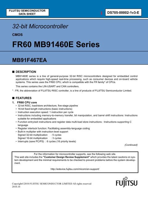
FUJITSU SEMICONDUCTOR<br />
DATA SHEET<br />
32-bit Microcontroller<br />
CMOS<br />
<strong>FR60</strong> <strong>MB91460E</strong> <strong>Series</strong><br />
MB91F467EA<br />
■ DESCRIPTION<br />
<strong>MB91460E</strong> series is a line of general-purpose 32-bit RISC microcontrollers designed for embedded control<br />
applications which require high-speed real-time processing, such as consumer devices and on-board vehicle<br />
systems. This series uses the <strong>FR60</strong> CPU, which is compatible with the FR family* of CPUs.<br />
This series contains the LIN-USART and CAN controllers.<br />
* : FR, the abbreviation of FUJITSU RISC controller, is a line of products of FUJITSU Semiconductor Limited.<br />
■ FEATURES<br />
1. <strong>FR60</strong> CPU core<br />
• 32-bit RISC, load/store architecture, five-stage pipeline<br />
• 16-bit fixed-length instructions (basic instructions)<br />
• Instruction execution speed: 1 instruction per cycle<br />
• Instructions including memory-to-memory transfer, bit manipulation, and barrel shift instructions: Instructions<br />
suitable for embedded applications<br />
• Function entry/exit instructions and register data multi-load store instructions : Instructions supporting C<br />
language<br />
• Register interlock function: Facilitating assembly-language coding<br />
• Built-in multiplier with instruction-level support<br />
Signed 32-bit multiplication : 5 cycles<br />
Signed 16-bit multiplication : 3 cycles<br />
• Interrupts (save PC/PS) : 6 cycles (16 priority levels)<br />
(Continued)<br />
For the information for microcontroller supports, see the following web site.<br />
This web site includes the "Customer Design Review Supplement" which provides the latest cautions on system<br />
development and the minimal requirements to be checked to prevent problems before the system development.<br />
http://edevice.fujitsu.com/micom/en-support/<br />
Copyright©2010 FUJITSU SEMICONDUCTOR LIMITED All rights reserved<br />
2010.10<br />
DS705-00002-1v3-E
<strong>MB91460E</strong> <strong>Series</strong><br />
(Continued)<br />
• Harvard architecture enabling program access and data access to be performed simultaneously<br />
• Instructions compatible with the FR family<br />
2. Internal peripheral resources<br />
• General-purpose ports : Maximum 170 ports<br />
• DMAC (DMA Controller)<br />
Maximum of 5 channels able to operate simultaneously. (External to external : 1 channel)<br />
3 transfer sources (external pin/internal peripheral/software)<br />
Activation source can be selected using software.<br />
Addressing mode specifies full 32-bit addresses (increment/decrement/fixed)<br />
Transfer mode (demand transfer/burst transfer/step transfer/block transfer)<br />
Transfer data size selectable from 8/16/32-bit<br />
Multi-byte transfer enabled (by software)<br />
DMAC descriptor in I/O areas (200H to 240H, 1000H to 1024H)<br />
• A/D converter (successive approximation type)<br />
10-bit resolution: 24 channels<br />
Conversion time: minimum 1 µs<br />
• External interrupt inputs : 14 channels<br />
8 channels shared with CAN RX or I2C pins<br />
• Bit search module (for REALOS)<br />
Function to search from the MSB (most significant bit) for the position of the first “0”, “1”, or changed bit in a word<br />
• LIN-USART (full duplex double buffer): 5 channels<br />
Clock synchronous/asynchronous selectable<br />
Sync-break detection<br />
Internal dedicated baud rate generator<br />
• I 2 C* bus interface (supports 400 kbps): 3 channels<br />
Master/slave transmission and reception<br />
Arbitration function, clock synchronization function<br />
• CAN controller (C-CAN): 2 channels<br />
Maximum transfer speed: 1 Mbps<br />
32 transmission/reception message buffers<br />
• Stepper motor controller : 6 channels<br />
4 high current output to each channel<br />
2 synchronized PWMs per channel (8/10-bit)<br />
• Sound generator : 1 channel<br />
Tone frequency : PWM frequency divide-by-two (reload value + 1)<br />
• Alarm comparator : 1 channel<br />
Monitor external voltage<br />
Generate an interrupt in case of voltage lower/higher than the defined thresholds (reference voltage)<br />
• 16-bit PPG timer : 12 channels<br />
• 16-bit PFM timer : 1 channel<br />
• 16-bit reload timer: 8 channels<br />
• 16-bit free-run timer: 8 channels (1 channel each for ICU and OCU)<br />
• Input capture: 8 channels (operates in conjunction with the free-run timer)<br />
• Output compare: 4 channels (operates in conjunction with the free-run timer)<br />
• Up/Down counter: 3 channels (3*8-bit or 1*16-bit + 1*8-bit)<br />
• Watchdog timer<br />
(Continued)<br />
2 DS705-00002-1v3-E
<strong>MB91460E</strong> <strong>Series</strong><br />
(Continued)<br />
• Real-time clock<br />
• Low-power consumption modes : Sleep/stop mode function<br />
• Supply Supervisor: Low voltage detection circuit for external VDD5 and internal 1.8V core voltage<br />
• Clock supervisor<br />
Monitors the sub-clock (32 kHz) and the main clock (4 MHz) , and switches to a recovery clock (CR oscillator,<br />
etc.) when the oscillations stop.<br />
• Clock modulator<br />
• Clock monitor<br />
• Sub-clock calibration<br />
Corrects the real-time clock timer when operating with the 32 kHz or CR oscillator<br />
• Main oscillator stabilization timer<br />
Generates an interrupt in sub-clock mode after the stabilization wait time has elapsed on the 23-bit stabilization<br />
wait time counter<br />
• Sub-oscillator stabilization timer<br />
Generates an interrupt in main clock mode after the stabilization wait time has elapsed on the 15-bit stabilization<br />
wait time counter<br />
3. Shutdown mode<br />
• In low leakage shutdown mode, the internal main power supply is switched off. Only the following resources<br />
and meories remain active:<br />
- Standby RAM (16 KByte)<br />
- Real Time Clock<br />
- 4 MHz oscillator, 32 kHz oscillator, RC oscillator<br />
- Power management logic<br />
- Hardware Watchdog and Clock Supervisor<br />
4. Package and technology<br />
• Package : LQFP-208 (low profile QFP)<br />
• CMOS 0.18 µm technology<br />
• Power supply range 3 V to 5 V (1.9V/1.8 V internal logic provided by a step-down voltage converter)<br />
• Operating temperature range: between − 40˚C and + 105˚C<br />
DS705-00002-1v3-E 3
<strong>MB91460E</strong> <strong>Series</strong><br />
■ PRODUCT LINEUP<br />
Feature MB91FV460B<br />
MB91F467DA<br />
MB91F467DB<br />
MB91F467EA<br />
Max. core frequency (CLKB) 100MHz 96MHz 100MHz<br />
Max. resource frequency (CLKP) 50MHz 48MHz 50MHz<br />
Max. external bus freq. (CLKT) 50MHz 48MHz 50MHz<br />
Max. CAN frequency (CLKCAN) 50MHz 48MHz 50MHz<br />
Technology 0.18um 0.18um 0.18um<br />
Software-Watchdog yes yes yes<br />
Hardware-Watchdog<br />
(RC osc. based)<br />
yes (disengageable),<br />
can be activated in<br />
SLEEP/STOP<br />
4 DS705-00002-1v3-E<br />
yes<br />
yes,<br />
can be activated in<br />
SLEEP/STOP<br />
Bit Search yes yes yes<br />
Reset input (INITX) yes yes yes<br />
Clock Modulator yes yes yes<br />
Clock Monitor yes yes yes<br />
Low Power Mode yes yes yes<br />
Shutdown Mode<br />
no,<br />
emulation by software<br />
no yes<br />
DMA 5 ch 5 ch 5 ch<br />
MMU/MPU MPU (16 ch) 1) MPU (8 ch) 1) MPU (8 ch) 1)<br />
Flash memory<br />
2112 KByte or external<br />
emulation SRAM<br />
1088 KByte 1088 KByte<br />
Flash Protection yes yes yes<br />
D-RAM 64 KByte 32 KByte 64 KByte<br />
ID-RAM 64 KByte 32 KByte 48 KByte<br />
Standby RAM no no 16 KByte<br />
Flash-Cache (F-cache) 16 KByte 8 KByte 8 KByte<br />
Boot-ROM / BI-ROM 16 KByte Boot Flash 4 KByte 4 KByte<br />
RTC 1 ch 1 ch 1 ch<br />
Free Running Timer 8 ch 8 ch 8 ch<br />
ICU 8 ch 8 ch 8 ch<br />
OCU 8 ch 4 ch 4 ch<br />
Reload Timer 8 ch 8 ch 8 ch<br />
PPG 16-bit 16 ch 12 ch 12 ch<br />
PFM 16-bit 1 ch 1 ch 1 ch
<strong>MB91460E</strong> <strong>Series</strong><br />
Sound Generator 1 ch 1 ch 1 ch<br />
Up/Down Counter (8/16-bit) 4 ch (8-bit)/2ch(16-bit) 3 ch (8-bit) / 1 ch (16-bit) 3 ch (8-bit)/1ch(16-bit)<br />
C_CAN 6 ch (128msg) 3 ch (32msg) 2 ch (32msg)<br />
LIN-USART 16 ch FIFO 1 ch + 4 ch FIFO 1 ch + 4 ch FIFO<br />
I2C (400k) 8 ch 3 ch 3 ch<br />
FR external bus<br />
yes (32bit addr,<br />
32bit data)<br />
yes (26bit addr,<br />
32bit data)<br />
yes (26bit addr,<br />
32bit data)<br />
External Interrupts 32 ch 14 ch 14 ch<br />
SMC 6 ch 6 ch 6 ch<br />
ADC (10 bit)<br />
Feature MB91FV460B<br />
32 ch, with<br />
Range Comparator<br />
MB91F467DA<br />
MB91F467DB<br />
DS705-00002-1v3-E 5<br />
24 ch<br />
MB91F467EA<br />
24 ch, with<br />
Range Comparator<br />
Alarm Comparator 2 ch 1 ch 1 ch<br />
Supply Supervisor<br />
(low voltage detection)<br />
yes yes yes<br />
Clock Supervisor yes yes yes<br />
Main clock oscillator 4MHz 4MHz 4MHz<br />
Sub clock oscillator 32kHz 32kHz 32kHz<br />
RC Oscillator 100kHz / 2MHz 100kHz / 2MHz 100kHz / 2MHz<br />
PLL x 25 x 24 x 25<br />
DSU4 yes - -<br />
EDSU yes (32 BP) *1 yes (16 BP) *1 yes (16 BP) *1<br />
Supply Voltage 1.8V + 3V / 5V 3V / 5V 3V / 5V<br />
Regulator no yes yes<br />
Power Consumption n.a. < 2 W < 1.3 W<br />
Temperatur Range (Ta) 0..70 C -40..105 C -40..105 C<br />
Package BGA896 QFP208 LQFP208
<strong>MB91460E</strong> <strong>Series</strong><br />
Feature MB91FV460B<br />
MB91F467DA<br />
MB91F467DB<br />
Power on to PLL run < 20 ms < 20 ms < 20 ms<br />
Flash Download Time < 8 sec typical < 6 sec typical < 6 sec typical<br />
*1 : MPU channels use EDSU breakpoint registers (shared operation between MPU and EDSU).<br />
MB91F467EA<br />
6 DS705-00002-1v3-E
<strong>MB91460E</strong> <strong>Series</strong><br />
DS705-00002-1v3-E 7<br />
■ PIN ASSIGNMENT<br />
1. MB91F467EA<br />
(TOP VIEW)<br />
FPT-208P-M06<br />
Note: Difference versus MB91460D series: At pins 95+96, RX2 and TX2 of CAN2 are removed.<br />
1<br />
2<br />
3<br />
4<br />
5<br />
6<br />
7<br />
8<br />
9<br />
10<br />
11<br />
12<br />
13<br />
14<br />
15<br />
16<br />
17<br />
18<br />
19<br />
20<br />
21<br />
22<br />
23<br />
24<br />
25<br />
26<br />
27<br />
28<br />
29<br />
30<br />
31<br />
32<br />
33<br />
34<br />
35<br />
36<br />
37<br />
38<br />
39<br />
40<br />
41<br />
42<br />
43<br />
44<br />
45<br />
46<br />
47<br />
48<br />
49<br />
50<br />
51<br />
52<br />
156<br />
155<br />
154<br />
153<br />
152<br />
151<br />
150<br />
149<br />
148<br />
147<br />
146<br />
145<br />
144<br />
143<br />
142<br />
141<br />
140<br />
139<br />
138<br />
137<br />
136<br />
135<br />
134<br />
133<br />
132<br />
131<br />
130<br />
129<br />
128<br />
127<br />
126<br />
125<br />
124<br />
123<br />
122<br />
121<br />
120<br />
119<br />
118<br />
117<br />
116<br />
115<br />
114<br />
113<br />
112<br />
111<br />
110<br />
109<br />
108<br />
107<br />
106<br />
105<br />
VDD5<br />
P29_7/AN7<br />
P29_6/AN6<br />
P29_5/AN5<br />
P29_4/AN4<br />
P29_3/AN3<br />
P29_2/AN2<br />
P29_1/AN1<br />
P29_0/AN0<br />
ALARM_0<br />
AVCC5<br />
AVRH5<br />
AVSS5<br />
P16_7/PPG15/ATGX<br />
P16_6/PPG14/PFM<br />
P16_5/PPG13/SGO<br />
P16_4/PPG12/SGA<br />
P16_3/PPG11<br />
P16_2/PPG10<br />
P16_1/PPG9<br />
P16_0/PPG8<br />
P17_7/PPG7<br />
P17_6/PPG6<br />
P17_5/PPG5<br />
P17_4/PPG4<br />
VSS5<br />
VDD5<br />
P14_7/ICU7/TIN7/TTG7/15<br />
P14_6/ICU6/TIN6/TTG6/14<br />
P14_5/ICU5/TIN5/TTG5/13<br />
P14_4/ICU4/TIN4/TTG4/12<br />
P14_3/ICU3/TIN3/TTG11<br />
P14_2/ICU2/TIN2/TTG10<br />
P14_1/ICU1/TIN1/TTG9<br />
P14_0/ICU0/TIN0/TTG8<br />
P15_3/OCU3/TOT3<br />
P15_2/OCU2/TOT2<br />
P15_1/OCU1/TOT1<br />
P15_0/OCU0/TOT0<br />
P18_6/SCK7/ZIN3/CK7<br />
P18_5/SOT7/BIN3<br />
P18_4/SIN7/AIN3<br />
P18_2/SCK6/ZIN2/CK6<br />
P18_1/SOT6/BIN2<br />
P18_0/SIN6/AIN2<br />
P19_6/SCK5/CK5<br />
P19_5/SOT5<br />
P19_4/SIN5<br />
P19_2/SCK4/CK4<br />
P19_1/SOT4<br />
P19_0/SIN4<br />
VSS5<br />
VSS5<br />
P01_0/D16<br />
P01_1/D17<br />
P01_2/D18<br />
P01_3/D19<br />
P01_4/D20<br />
P01_5/D21<br />
P01_6/D22<br />
P01_7/D23<br />
P00_0/D24<br />
P00_1/D25<br />
P00_2/D26<br />
P00_3/D27<br />
P00_4/D28<br />
P00_5/D29<br />
P00_6/D30<br />
P00_7/D31<br />
P07_0/A0<br />
P07_1/A1<br />
P07_2/A2<br />
P07_3/A3<br />
P07_4/A4<br />
P07_5/A5<br />
P07_6/A6<br />
P07_7/A7<br />
VDD35<br />
VSS5<br />
P06_0/A8<br />
P06_1/A9<br />
P06_2/A10<br />
P06_3/A11<br />
P06_4/A12<br />
P06_5/A13<br />
P06_6/A14<br />
P06_7/A15<br />
P05_0/A16<br />
P05_1/A17<br />
P05_2/A18<br />
P05_3/A19<br />
P05_4/A20<br />
P05_5/A21<br />
P05_6/A22<br />
P05_7/A23<br />
P04_0/A24<br />
P04_1/A25<br />
P08_0/WRX0<br />
P08_1/WRX1<br />
P08_2/WRX2<br />
P08_3/WRX3<br />
P08_4/RDX<br />
P08_5/BGRNTX<br />
VDD35<br />
53<br />
54<br />
55<br />
56<br />
57<br />
58<br />
59<br />
60<br />
61<br />
62<br />
63<br />
64<br />
65<br />
66<br />
67<br />
68<br />
69<br />
70<br />
71<br />
72<br />
73<br />
74<br />
75<br />
76<br />
77<br />
78<br />
79<br />
80<br />
81<br />
82<br />
83<br />
84<br />
85<br />
86<br />
87<br />
88<br />
89<br />
90<br />
91<br />
92<br />
93<br />
94<br />
95<br />
96<br />
97<br />
98<br />
99<br />
100<br />
101<br />
102<br />
103<br />
104<br />
208<br />
207<br />
206<br />
205<br />
204<br />
203<br />
202<br />
201<br />
200<br />
199<br />
198<br />
197<br />
196<br />
195<br />
194<br />
193<br />
192<br />
191<br />
190<br />
189<br />
188<br />
187<br />
186<br />
185<br />
184<br />
183<br />
182<br />
181<br />
180<br />
179<br />
178<br />
177<br />
176<br />
175<br />
174<br />
173<br />
172<br />
171<br />
170<br />
169<br />
168<br />
167<br />
166<br />
165<br />
164<br />
163<br />
162<br />
161<br />
160<br />
159<br />
158<br />
157<br />
VDD35<br />
P02_7/D15<br />
P02_6/D14<br />
P02_5/D13<br />
P02_4/D12<br />
P02_3/D11<br />
P02_2/D10<br />
P02_1/D9<br />
P02_0/D8<br />
P03_7/D7<br />
P03_6/D6<br />
P03_5/D5<br />
P03_4/D4<br />
P03_3/D3<br />
P03_2/D2<br />
P03_1/D1<br />
P03_0/D0<br />
P13_2/DEOTX0/DEOP0<br />
P13_1/DACKX0<br />
P13_0/DREQ0<br />
VSS5<br />
P25_7/SMC2M5<br />
P25_6/SMC2P5<br />
P25_5/SMC1M5<br />
P25_4/SMC1P5<br />
HVSS5<br />
HVDD5<br />
P25_3/SMC2M4<br />
P25_2/SMC2P4<br />
P25_1/SMC1M4<br />
P25_0/SMC1P4<br />
P26_7/SMC2M3/AN31<br />
P26_6/SMC2P3/AN30<br />
P26_5/SMC1M3/AN29<br />
P26_4/SMC1P3/AN28<br />
HVSS5<br />
HVDD5<br />
P26_3/SMC2M2/AN27<br />
P26_2/SMC2P2/AN26<br />
P26_1/SMC1M2/AN25<br />
P26_0/SMC1P2/AN24<br />
P27_7/SMC2M1/AN23<br />
P27_6/SMC2P1/AN22<br />
P27_5/SMC1M1/AN21<br />
P27_4/SMC1P1/AN20<br />
HVSS5<br />
HVDD5<br />
P27_3/SMC2M0/AN19<br />
P27_2/SMC2P0/AN18<br />
P27_1/SMC1M0/AN17<br />
P27_0/SMC1P0/AN16<br />
VSS5<br />
VSS5<br />
P08_6/BRQ<br />
P08_7/RDY<br />
P09_0/CSX0<br />
P09_1/CSX1<br />
P09_2/CSX2<br />
P09_3/CSX3<br />
P09_6/CSX6<br />
P09_7/CSX7<br />
P10_1/ASX<br />
P10_2/BAAX<br />
P10_3/WEX<br />
P10_4/MCLKO<br />
P10_5/MCLKI<br />
P10_6/MCLKE<br />
MONCLK<br />
VSS5<br />
MD_2<br />
MD_1<br />
MD_0<br />
INITX<br />
X1A<br />
X0A<br />
X1<br />
X0<br />
VDD5<br />
VSS5<br />
VCC18C<br />
VDD5R<br />
VDD5R<br />
P24_0/INT0<br />
P24_1/INT1<br />
P24_2/INT2<br />
P24_3/INT3<br />
P24_4/INT4/SDA2<br />
P24_5/INT5/SCL2<br />
P24_6/INT6/SDA3<br />
P24_7/INT7/SCL3<br />
P23_0/RX0/INT8<br />
P23_1/TX0<br />
P23_2/RX1/INT9<br />
P23_3/TX1<br />
P23_4/INT10<br />
P23_5<br />
P22_0/INT12<br />
P22_2/INT13<br />
P22_4/SDA0/INT14<br />
P22_5/SCL0<br />
P20_0/SIN2/AIN0<br />
P20_1/SOT2/BIN0<br />
P20_2/SCK2/ZIN0/CK2<br />
VDD5<br />
QFP-208
<strong>MB91460E</strong> <strong>Series</strong><br />
■ PIN DESCRIPTION<br />
1. MB91F467EA<br />
Pin no. Pin name I/O<br />
2 to 9<br />
10 to 17<br />
18 to 25<br />
28 to 35<br />
36 to 43<br />
44, 45<br />
46 to 49<br />
50<br />
51<br />
54<br />
55<br />
56 to 59<br />
60, 61<br />
62<br />
63<br />
64<br />
65<br />
I/O circuit<br />
type * 1<br />
Function<br />
P01_0 to P01_7<br />
General-purpose input/output ports<br />
I/O A<br />
D16 to D23 Signal pins of external data bus (bit16 to bit23)<br />
P00_0 to P00_7<br />
General-purpose input/output ports<br />
I/O A<br />
D24 to D31 Signal pins of external data bus (bit24 to bit31)<br />
P07_0 to P07_7<br />
General-purpose input/output ports<br />
I/O A<br />
A0 to A7 Signal pins of external address bus (bit0 to bit7)<br />
P06_0 to P06_7<br />
General-purpose input/output ports<br />
I/O A<br />
A8 to A15 Signal pins of external address bus (bit8 to bit15)<br />
P05_0 to P05_7<br />
General-purpose input/output ports<br />
I/O A<br />
A16 to A23 Signal pins of external address bus (bit16 to bit23)<br />
P04_0, P04_1<br />
General-purpose input/output ports<br />
I/O A<br />
A24, A25 Signal pins of external address bus (bit24, bit25)<br />
P08_0 to P08_3<br />
General-purpose input/output ports<br />
I/O A<br />
WRX0 to WRX3 External write strobe output pins<br />
P08_4<br />
General-purpose input/output port<br />
I/O A<br />
RDX External read strobe output pin<br />
P08_5<br />
General-purpose input/output port<br />
I/O A<br />
BGRNTX External bus release reception output pin<br />
P08_6<br />
General-purpose input/output port<br />
I/O A<br />
BRQ External bus release request input pin<br />
P08_7<br />
General-purpose input/output port<br />
I/O A<br />
RDY External ready input pin<br />
P09_0 to P09_3<br />
General-purpose input/output ports<br />
I/O A<br />
CSX0 to CSX3 Chip select output pins<br />
P09_6, P09_7<br />
General-purpose input/output ports<br />
I/O A<br />
CSX6, CSX7 Chip select output pins<br />
P10_1<br />
General-purpose input/output port<br />
I/O A<br />
ASX Address strobe output pin<br />
P10_2<br />
General-purpose input/output port<br />
I/O A<br />
BAAX Burst address advance output pin<br />
P10_3<br />
General-purpose input/output port<br />
I/O A<br />
WEX Write enable output pin<br />
P10_4<br />
General-purpose input/output port<br />
I/O A<br />
MCLKO Clock output pin for memory<br />
(Continued)<br />
8 DS705-00002-1v3-E
(Continued)<br />
Pin no. Pin name I/O<br />
66<br />
I/O circuit<br />
type *1<br />
<strong>MB91460E</strong> <strong>Series</strong><br />
Function<br />
P10_5<br />
General-purpose input/output port<br />
I/O A<br />
MCLKI Clock input pin for memory<br />
67<br />
P10_6<br />
MCLKE<br />
I/O A<br />
General-purpose input/output port<br />
Clock enable signal pin for memory<br />
68 MONCLK O M Clock monitor pin<br />
70 MD_2 I G<br />
71 MD_1 I G Mode setting pins<br />
72 MD_0 I G<br />
73 INITX I H External reset input pin<br />
74 X1A ⎯ J2 Sub clock (oscillation) output<br />
75 X0A ⎯ J2 Sub clock (oscillation) input<br />
76 X1 ⎯ J1 Clock (oscillation) output<br />
77 X0 ⎯ J1 Clock (oscillation) input<br />
83 to 86<br />
87<br />
88<br />
89<br />
90<br />
91<br />
92<br />
93<br />
P24_0 to P24_3<br />
General-purpose input/output ports<br />
I/O A<br />
INT0 to INT3 External interrupt input pins<br />
P24_4<br />
General-purpose input/output port<br />
INT4 I/O C External interrupt input pin<br />
SDA2 I2C bus DATA input/output pin<br />
P24_5<br />
General-purpose input/output port<br />
INT5 I/O C External interrupt input pin<br />
SCL2 I2C bus clock input/output pin<br />
P24_6<br />
General-purpose input/output port<br />
INT6 I/O C External interrupt input pin<br />
SDA3 I2C bus DATA input/output pin<br />
P24_7<br />
General-purpose input/output port<br />
INT7 I/O C External interrupt input pin<br />
SCL3 I2C bus clock input/output pin<br />
P23_0<br />
General-purpose input/output port<br />
RX0 I/O A RX input pin of CAN0<br />
INT8 External interrupt input pin<br />
P23_1<br />
General-purpose input/output port<br />
I/O A<br />
TX0 TX output pin of CAN0<br />
P23_2<br />
General-purpose input/output port<br />
RX1 I/O A RX input pin of CAN1<br />
INT9 External interrupt input pin<br />
(Continued)<br />
DS705-00002-1v3-E 9
<strong>MB91460E</strong> <strong>Series</strong><br />
(Continued)<br />
Pin no. Pin name I/O<br />
I/O circuit<br />
type *1<br />
Function<br />
94<br />
P23_3<br />
TX1<br />
I/O A<br />
General-purpose input/output port<br />
TX output pin of CAN1<br />
95 *2<br />
P23_4<br />
INT10<br />
I/O A<br />
General-purpose input/output port<br />
External interrupt input pin<br />
96 *2 P23_5 I/O A General-purpose input/output port<br />
97<br />
98<br />
99<br />
100<br />
101<br />
102<br />
103<br />
106<br />
107<br />
108<br />
P22_0<br />
General-purpose input/output port<br />
I/O A<br />
INT12 External interrupt input pin<br />
P22_2<br />
General-purpose input/output port<br />
I/O A<br />
INT13 External interrupt input pin<br />
P22_4<br />
General-purpose input/output port<br />
SDA0 I/O C I2C bus data input/output pin<br />
INT14 External interrupt input pin<br />
P22_5<br />
General-purpose input/output port<br />
I/O C<br />
SCL0 I2C bus clock input/output pin<br />
P20_0<br />
General-purpose input/output port<br />
SIN2 I/O A Data input pin of USART2<br />
AIN0 Up/down counter input pin<br />
P20_1<br />
General-purpose input/output port<br />
SOT2 I/O A Data output pin of USART2<br />
BIN0 Up/down counter input pin<br />
P20_2<br />
General-purpose input/output port<br />
SCK2<br />
ZIN0<br />
I/O A<br />
Clock input/output pin of USART2<br />
Up/down counter input pin<br />
CK2 External clock input pin of free-run timer 2<br />
P19_0<br />
General-purpose input/output port<br />
I/O A<br />
SIN4 Data input pin of USART4<br />
P19_1<br />
General-purpose input/output port<br />
I/O A<br />
SOT4 Data output pin of USART4<br />
P19_2<br />
General-purpose input/output port<br />
SCK4 I/O A Clock input/output pin of USART4<br />
CK4 External clock input pin of free-run timer 4<br />
(Continued)<br />
10 DS705-00002-1v3-E
(Continued)<br />
Pin no. Pin name I/O<br />
109<br />
110<br />
111<br />
112<br />
113<br />
114<br />
115<br />
116<br />
117<br />
118 to 121<br />
122 to 129<br />
I/O circuit<br />
type *1<br />
<strong>MB91460E</strong> <strong>Series</strong><br />
Function<br />
P19_4<br />
General-purpose input/output port<br />
I/O A<br />
SIN5 Data input pin of USART5<br />
P19_5<br />
General-purpose input/output port<br />
I/O A<br />
SOT5 Data output pin of USART5<br />
P19_6<br />
General-purpose input/output port<br />
SCK5 I/O A Clock input/output pin of USART5<br />
CK5 External clock input pin of free-run timer 5<br />
P18_0<br />
General-purpose input/output port<br />
SIN6 I/O A Data input pin of USART6<br />
AIN2 Up/down counter input pin<br />
P18_1<br />
General-purpose input/output port<br />
SOT6 I/O A Data output pin of USART6<br />
BIN2 Up/down counter input pin<br />
P18_2<br />
General-purpose input/output port<br />
SCK6<br />
ZIN2<br />
I/O A<br />
Clock input/output pin of USART6<br />
Up/down counter input pin<br />
CK6 External clock input pin of free-run timer 6<br />
P18_4<br />
General-purpose input/output port<br />
SIN7 I/O A Data input pin of USART7<br />
AIN3 Up/down counter input pin<br />
P18_5<br />
General-purpose input/output port<br />
SOT7 I/O A Data output pin of USART7<br />
BIN3 Up/down counter input pin<br />
P18_6<br />
General-purpose input/output port<br />
SCK7<br />
ZIN3<br />
I/O A<br />
Clock input/output pin of USART7<br />
Up/down counter input pin<br />
CK7 External clock input pin of free-run timer 7<br />
P15_0 to P15_3<br />
General-purpose input/output ports<br />
OCU0 to OCU3 I/O A Output compare output pins<br />
TOT0 to TOT3 Reload timer output pins<br />
P14_0 to P14_7<br />
General-purpose input/output ports<br />
ICU0 to ICU7 Input capture input pins<br />
TIN0 to TIN7<br />
TTG8 to TTG11,<br />
I/O A External trigger input pins of reload timer<br />
TTG4/12 to<br />
TTG7/15<br />
External trigger input pins of PPG timer<br />
(Continued)<br />
DS705-00002-1v3-E 11
<strong>MB91460E</strong> <strong>Series</strong><br />
(Continued)<br />
Pin no. Pin name I/O<br />
132 to 135<br />
136 to 139<br />
140<br />
141<br />
142<br />
I/O circuit<br />
type *1<br />
Function<br />
P17_4 to P17_7<br />
General-purpose input/output ports<br />
I/O A<br />
PPG4 to PPG7 Output pins of PPG timer<br />
P16_0 to P16_3<br />
General-purpose input/output ports<br />
I/O A<br />
PPG8 to PPG11 PPG timer output pins<br />
P16_4<br />
General-purpose input/output port<br />
PPG12 I/O A Output pin of PPG timer<br />
SGA SGA output pin of sound generator<br />
P16_5<br />
General-purpose input/output port<br />
PPG13 I/O A Output pin of PPG timer<br />
SGO SGO output pin of sound generator<br />
P16_6<br />
General-purpose input/output port<br />
PPG14 I/O A Output pin of PPG timer<br />
PFM Pulse frequency modulator output pin<br />
P16_7<br />
General-purpose input/output port<br />
143 PPG15 I/O A PPG timer output pin<br />
ATGX A/D converter external trigger input pin<br />
147 ALARM_0 I N Alarm comparator input pin<br />
148 to 155<br />
158<br />
159<br />
160<br />
161<br />
164<br />
P29_0 to P29_7<br />
General-purpose input/output ports<br />
I/O B<br />
AN0 to AN7 Analog input pins of A/D converter<br />
P27_0<br />
General-purpose input/output port<br />
SMC1P0 I/O F Controller output pin of Stepper motor<br />
AN16 Analog input pin of A/D converter<br />
P27_1<br />
General-purpose input/output port<br />
SMC1M0 I/O F Controller output pin of Stepper motor<br />
AN17 Analog input pin of A/D converter<br />
P27_2<br />
General-purpose input/output port<br />
SMC2P0 I/O F Controller output pin of Stepper motor<br />
AN18 Analog input pin of A/D converter<br />
P27_3<br />
General-purpose input/output port<br />
SMC2M0 I/O F Controller output pin of Stepper motor<br />
AN19 Analog input pin of A/D converter<br />
P27_4<br />
General-purpose input/output port<br />
SMC1P1 I/O F Controller output pin of Stepper motor<br />
AN20 Analog input pin of A/D converter<br />
(Continued)<br />
12 DS705-00002-1v3-E
(Continued)<br />
Pin no. Pin name I/O<br />
165<br />
166<br />
167<br />
168<br />
169<br />
170<br />
171<br />
174<br />
175<br />
176<br />
177<br />
I/O circuit<br />
type *1<br />
<strong>MB91460E</strong> <strong>Series</strong><br />
Function<br />
P27_5<br />
General-purpose input/output port<br />
SMC1M1 I/O F Controller output pin of Stepper motor<br />
AN21 Analog input pin of A/D converter<br />
P27_6<br />
General-purpose input/output port<br />
SMC2P1 I/O F Controller output pin of Stepper motor<br />
AN22 Analog input pin of A/D converter<br />
P27_7<br />
General-purpose input/output port<br />
SMC2M1 I/O F Controller output pin of Stepper motor<br />
AN23 Analog input pin of A/D converter<br />
P26_0<br />
General-purpose input/output port<br />
SMC1P2 I/O F Controller output pin of Stepper motor<br />
AN24 Analog input pin of A/D converter<br />
P26_1<br />
General-purpose input/output port<br />
SMC1M2 I/O F Controller output pin of Stepper motor<br />
AN25 Analog input pin of A/D converter<br />
P26_2<br />
General-purpose input/output port<br />
SMC2P2 I/O F Controller output pin of Stepper motor<br />
AN26 Analog input pin of A/D converter<br />
P26_3<br />
General-purpose input/output port<br />
SMC2M2 I/O F Controller output pin of Stepper motor<br />
AN27 Analog input pin of A/D converter<br />
P26_4<br />
General-purpose input/output port<br />
SMC1P3 I/O F Controller output pin of Stepper motor<br />
AN28 Analog input pin of A/D converter<br />
P26_5<br />
General-purpose input/output port<br />
SMC1M3 I/O F Controller output pin of Stepper motor<br />
AN29 Analog input pin of A/D converter<br />
P26_6<br />
General-purpose input/output port<br />
SMC2P3 I/O F Controller output pin of Stepper motor<br />
AN30 Analog input pin of A/D converter<br />
P26_7<br />
General-purpose input/output port<br />
SMC2M3 I/O F Controller output pin of Stepper motor<br />
AN31 Analog input pin of A/D converter<br />
(Continued)<br />
DS705-00002-1v3-E 13
<strong>MB91460E</strong> <strong>Series</strong><br />
(Continued)<br />
Pin no. Pin name I/O<br />
178<br />
179<br />
180<br />
181<br />
184<br />
185<br />
186<br />
187<br />
189<br />
190<br />
191<br />
192 to 199<br />
200 to 207<br />
I/O circuit<br />
type *1<br />
Function<br />
P25_0<br />
General-purpose input/output port<br />
I/O E<br />
SMC1P4 Controller output pin of Stepper motor<br />
P25_1<br />
General-purpose input/output port<br />
I/O E<br />
SMC1M4 Controller output pin of Stepper motor<br />
P25_2<br />
General-purpose input/output port<br />
I/O E<br />
SMC2P4 Controller output pin of Stepper motor<br />
P25_3<br />
General-purpose input/output port<br />
I/O E<br />
SMC2M4 Controller output pin of Stepper motor<br />
P25_4<br />
General-purpose input/output port<br />
I/O E<br />
SMC1P5 Controller output pin of Stepper motor<br />
P25_5<br />
General-purpose input/output port<br />
I/O E<br />
SMC1M5 Controller output pin of Stepper motor<br />
P25_6<br />
General-purpose input/output port<br />
I/O E<br />
SMC2P5 Controller output pin of Stepper motor<br />
P25_7<br />
General-purpose input/output port<br />
I/O E<br />
SMC2M5 Controller output pin of Stepper motor<br />
P13_0<br />
General-purpose input/output port<br />
I/O A<br />
DREQ0 DMA external transfer request input<br />
P13_1<br />
General-purpose input/output port<br />
I/O A<br />
DACKX0 DMA external transfer acknowledge output pin<br />
P13_2<br />
General-purpose input/output port<br />
DEOTX0 I/O A DMA external transfer EOT (End of Track) output pin<br />
DEOP0 DMA external transfer EOP (End of Process) output pin<br />
P03_0 to P03_7<br />
General-purpose input/output ports<br />
I/O A<br />
D0 to D7 Signal pins of external data bus (bit0 to bit7)<br />
P02_0 to P02_7<br />
General-purpose input/output ports<br />
I/O A<br />
D8 to D15 Signal pins of external data bus (bit8 to bit15)<br />
*1 : For information about the I/O circuit type, refer to “■ I/O CIRCUIT TYPES”.<br />
*2 : Difference versus MB91460D series: At pins 95+96, RX2 and TX2 of CAN2 are removed.<br />
14 DS705-00002-1v3-E
2. Power supply/Ground pins<br />
<strong>MB91460E</strong> <strong>Series</strong><br />
Pin no. Pin name I/O Function<br />
1, 27, 53, 69, 79, 105,<br />
131, 157, 188<br />
VSS5<br />
Ground pins<br />
163, 173, 183 HVSS5 Ground pins for Stepper motor controller<br />
26, 52, 208 VDD35 Power supply pins for external data bus<br />
78, 104, 130, 156 VDD5 Power supply pins<br />
162, 172, 182 HVDD5 Supply Power supply pins for Stepper motor controller<br />
81, 82 VDD5R Power supply pins for internal regulator<br />
144 AVSS5 Analog ground pin for A/D converter<br />
146 AVCC5 Power supply pin for A/D converter<br />
145 AVRH5 Reference power supply pin for A/D converter<br />
80 VCC18C Capacitor connection pin for internal regulator<br />
DS705-00002-1v3-E 15
<strong>MB91460E</strong> <strong>Series</strong><br />
■ I/O CIRCUIT TYPES<br />
Type Circuit Remarks<br />
A<br />
pull-up control<br />
CMOS level output<br />
(programmable IOL = 5mA, IOH = -5mA<br />
driver strength<br />
and IOL = 2mA, IOH = -2mA)<br />
control<br />
2 different CMOS hysteresis inputs with input<br />
data line<br />
shutdown function<br />
Automotive input with input shutdown function<br />
TTL input with input shutdown function<br />
Programmable pull-up resistor: 50kΩ approx.<br />
R<br />
pull- down control<br />
CMOS hysteresis type1<br />
CMOS hysteresis type2<br />
Automotive inputs<br />
TTL input<br />
standby control for<br />
input shutdown<br />
B<br />
pull-up control<br />
CMOS level output<br />
(programmable IOL = 5mA, IOH = -5mA<br />
driver strength<br />
control<br />
and IOL = 2mA, IOH = -2mA)<br />
2 different CMOS hysteresis inputs with input<br />
data line<br />
pull- down control<br />
shutdown function<br />
Automotive input with input shutdown function<br />
TTL input with input shutdown function<br />
Programmable pull-up resistor: 50kΩ approx.<br />
Analog input<br />
R<br />
CMOS hysteresis type1<br />
CMOS hysteresis type2<br />
Automotive inputs<br />
TTL input<br />
standby control for<br />
input shutdown<br />
analog input<br />
16 DS705-00002-1v3-E
Type Circuit Remarks<br />
<strong>MB91460E</strong> <strong>Series</strong><br />
C<br />
pull-up control<br />
CMOS level output (IOL = 3mA, IOH = -3mA)<br />
2 different CMOS hysteresis inputs with input<br />
shutdown function<br />
Automotive input with input shutdown function<br />
data line<br />
TTL input with input shutdown function<br />
Programmable pull-up resistor: 50kΩ approx.<br />
R<br />
pull- down control<br />
CMOS hysteresis type1<br />
CMOS hysteresis type2<br />
Automotive inputs<br />
TTL input<br />
standby control for<br />
input shutdown<br />
D<br />
pull-up control<br />
CMOS level output (IOL = 3mA, IOH = -3mA)<br />
2 different CMOS hysteresis inputs with input<br />
shutdown function<br />
Automotive input with input shutdown function<br />
data line<br />
TTL input with input shutdown function<br />
Programmable pull-up resistor: 50kΩ approx.<br />
Analog input<br />
R<br />
pull- down control<br />
CMOS hysteresis type1<br />
CMOS hysteresis type2<br />
Automotive inputs<br />
TTL input<br />
standby control for<br />
input shutdown<br />
analog input<br />
DS705-00002-1v3-E 17
<strong>MB91460E</strong> <strong>Series</strong><br />
Type Circuit Remarks<br />
E<br />
pull-up control<br />
CMOS level output<br />
(programmable IOL = 5mA, IOH = -5mA<br />
driver strength<br />
and IOL = 2mA, IOH = -2mA,<br />
control<br />
and IOL = 30mA, IOH = -30mA)<br />
data line<br />
2 different CMOS hysteresis inputs with input<br />
shutdown function<br />
Automotive input with input shutdown function<br />
TTL input with input shutdown function<br />
pull- down control<br />
Programmable pull-up resistor: 50kΩ approx.<br />
R<br />
CMOS hysteresis type1<br />
CMOS hysteresis type2<br />
Automotive inputs<br />
TTL input<br />
standby control for<br />
input shutdown<br />
F<br />
pull-up control<br />
CMOS level output<br />
(programmable IOL = 5mA, IOH = -5mA<br />
driver strength<br />
control<br />
and IOL = 2mA, IOH = -2mA,<br />
and IOL = 30mA, IOH = -30mA)<br />
data line<br />
2 different CMOS hysteresis inputs with input<br />
shutdown function<br />
Automotive input with input shutdown function<br />
TTL input with input shutdown function<br />
Programmable pull-up resistor: 50kΩ approx.<br />
pull- down control<br />
Analog input<br />
R<br />
CMOS hysteresis type1<br />
CMOS hysteresis type2<br />
Automotive inputs<br />
TTL input<br />
standby control for<br />
input shutdown<br />
analog input<br />
18 DS705-00002-1v3-E
Type Circuit Remarks<br />
G Mask ROM and EVA device:<br />
R<br />
Hysteresis<br />
inputs<br />
<strong>MB91460E</strong> <strong>Series</strong><br />
CMOS Hysteresis input pin<br />
Flash device:<br />
CMOS input pin<br />
12 V withstand (for MD [2:0])<br />
H CMOS Hysteresis input pin<br />
Pull-up resistor value: 50 kΩ approx.<br />
Pull-up<br />
Resistor<br />
R<br />
Hysteresis<br />
inputs<br />
J1 High-speed oscillation circuit:<br />
• Programmable between oscillation mode<br />
X1<br />
(external crystal or resonator connected<br />
to X0/X1 pins) and<br />
R<br />
Fast external Clock Input (FCI) mode<br />
(external clock connected to X0 pin)<br />
0<br />
1<br />
Xout • Feedback resistor = approx. 2 * 0.5 MΩ.<br />
Feedback resistor is grounded in the center<br />
when the oscillator is disabled or in FCI mode.<br />
X0<br />
R<br />
FCI or osc disable<br />
FCI<br />
J2 Low-speed oscillation circuit:<br />
• Feedback resistor = approx. 2 * 5 MΩ.<br />
X1A<br />
Xout Feedback resistor is grounded in the center<br />
when the oscillator is disabled.<br />
R<br />
X0A<br />
R<br />
osc disable<br />
DS705-00002-1v3-E 19
<strong>MB91460E</strong> <strong>Series</strong><br />
Type Circuit Remarks<br />
K<br />
pull-up control<br />
CMOS level output<br />
(programmable IOL = 5mA, IOH = -5mA<br />
driver strength<br />
and IOL = 2mA, IOH = -2mA)<br />
control<br />
2 different CMOS hysteresis inputs with input<br />
data line<br />
shutdown function<br />
Automotive input with input shutdown function<br />
TTL input with input shutdown function<br />
Programmable pull-up resistor: 50kΩ approx.<br />
pull- down control<br />
LCD SEG/COM output<br />
R<br />
CMOS hysteresis type1<br />
CMOS hysteresis type2<br />
Automotive inputs<br />
TTL input<br />
standby control for<br />
input shutdown<br />
LCD SEG/COM<br />
L<br />
pull-up control<br />
CMOS level output<br />
(programmable IOL = 5mA, IOH = -5mA<br />
driver strength<br />
control<br />
and IOL = 2mA, IOH = -2mA)<br />
2 different CMOS hysteresis inputs with input<br />
data line<br />
shutdown function<br />
Automotive input with input shutdown function<br />
TTL input with input shutdown function<br />
Programmable pull-up resistor: 50kΩ approx.<br />
Analog input<br />
pull- down control<br />
LCD Voltage input<br />
R<br />
CMOS hysteresis type1<br />
CMOS hysteresis type2<br />
Automotive inputs<br />
TTL input<br />
standby control for<br />
input shutdown<br />
VLCD<br />
20 DS705-00002-1v3-E
Type Circuit Remarks<br />
M CMOS level tri-state output<br />
(IOL = 5mA, IOH = -5mA)<br />
N<br />
tri-state control<br />
data line<br />
analog input line<br />
<strong>MB91460E</strong> <strong>Series</strong><br />
Analog input pin with protection<br />
DS705-00002-1v3-E 21
<strong>MB91460E</strong> <strong>Series</strong><br />
■ HANDLING DEVICES<br />
1. Preventing Latch-up<br />
Latch-up may occur in a CMOS IC if a voltage higher than (VDD5, VDD35 or HVDD5) or less than (VSS5 orHVSS5)<br />
is applied to an input or output pin or if a voltage exceeding the rating is applied between the power supply pins<br />
and ground pins. If latch-up occurs, the power supply current increases rapidly, sometimes resulting in thermal<br />
breakdown of the device. Therefore, be very careful not to apply voltages in excess of the absolute maximum<br />
ratings.<br />
2. Handling of unused input pins<br />
If unused input pins are left open, abnormal operation may result. Any unused input pins should be connected<br />
to pull-up or pull-down resistor (2KΩ to 10KΩ) or enable internal pullup or pulldown resisters (PPER/PPCR)<br />
before the input enable (PORTEN) is activated by software. The mode pins MD_x can be connected to VSS5 or<br />
VDD5 directly. Unused ALARM input pins can be connected to AVSS5 directly.<br />
3. Power supply pins<br />
In MB91460 series, devices including multiple power supply pins and ground pins are designed as follows; pins<br />
necessary to be at the same potential are interconnected internally to prevent malfunctions such as latch-up.<br />
All of the power supply pins and ground pins must be externally connected to the power supply and ground<br />
respectively in order to reduce unnecessary radiation, to prevent strobe signal malfunctions due to the ground<br />
level rising and to follow the total output current ratings. Furthermore, the power supply pins and ground pins of<br />
the MB91460 series must be connected to the current supply source via a low impedance.<br />
It is also recommended to connect a ceramic capacitor of approximately 0.1 µF as a bypass capacitor between<br />
power supply pin and ground pin near this device.<br />
This series has a built-in step-down regulator. Connect a bypass capacitor of 4.7 µF (use a X7R ceramic<br />
capacitator) to VCC18C pin for the regulator.<br />
4. Crystal oscillator circuit<br />
Noise in proximity to the X0 (X0A) and X1 (X1A) pins can cause the device to operate abnormally. Printed circuit<br />
boards should be designed so that the X0 (X0A) and X1 (X1A) pins, and crystal oscillator, as well as bypass<br />
capacitors connected to ground, are located near the device and ground.<br />
It is recommended that the printed circuit board layout be designed such that the X0 and X1 pins or X0A and<br />
X1A pins are surrounded by ground plane for the stable operation.<br />
Please request the oscillator manufacturer to evaluate the oscillational characteristics of the crystal and this<br />
device.<br />
5. Notes on using external clock<br />
When using the external clock, it is necessary to simultaneously supply the X0 (X0A) and the X1 (X1A) pins. In<br />
the described combination, X1 (X1A) should be supplied with a clock signal which has the opposite phase to<br />
the X0 (X0A) pins. At X0 and X1, a frequency up to 16 MHz is possible.<br />
(Continued)<br />
22 DS705-00002-1v3-E
(Continued)<br />
Example of using opposite phase supply<br />
X0 (X0A)<br />
X1 (X1A)<br />
<strong>MB91460E</strong> <strong>Series</strong><br />
DS705-00002-1v3-E 23
<strong>MB91460E</strong> <strong>Series</strong><br />
6. Mode pins (MD_x)<br />
These pins should be connected directly to the power supply or ground pins. To prevent the device from entering<br />
test mode accidentally due to noise, minimize the lengths of the patterns between each mode pin and power<br />
supply pin or ground pin on the printed circuit board as possible and connect them with low impedance.<br />
7. Notes on operating in PLL clock mode<br />
If the oscillator is disconnected or the clock input stops when the PLL clock is selected, the microcontroller may<br />
continue to operate at the free-running frequency of the self-oscillating circuit of the PLL. However, this selfrunning<br />
operation cannot be guaranteed.<br />
8. Pull-up control<br />
The AC standard is not guaranteed in case a pull-up resistor is connected to the pin serving as an external bus pin.<br />
9. Notes on PS register<br />
As the PS register is processed in advance by some instructions, when the debugger is being used, the exception<br />
handling may result in execution breaking in an interrupt handling routine or the displayed values of the flags in<br />
the PS register being updated.<br />
As the microcontroller is designed to carry out reprocessing correctly upon returning from such an EIT event,<br />
the operation before and after the EIT always proceeds according to specification.<br />
• The following behavior may occur if any of the following occurs in the instruction<br />
immediately after a DIV0U/DIV0S instruction:<br />
(a) a user interrupt or NMI is accepted;<br />
(b) single-step execution is performed;<br />
(c) execution breaks due to a data event or from the emulator menu.<br />
1. D0 and D1 flags are updated in advance.<br />
2. An EIT handling routine (user interrupt/NMI or emulator) is executed.<br />
3. Upon returning from the EIT, the DIV0U/DIV0S instruction is executed<br />
and the D0 and D1 flags are updated to the same values as those in 1.<br />
• The following behavior occurs when an ORCCR, STILM, MOV Ri,PS instruction is executed<br />
to enable a user interrupt or NMI source while that interrupt is in the active state.<br />
1. The PS register is updated in advance.<br />
2. An EIT handling routine (user interrupt/NMI or emulator) is executed.<br />
3. Upon returning from the EIT, the above instructions are executed and the PS register<br />
is updated to the same value as in 1.<br />
24 DS705-00002-1v3-E
■ NOTES ON DEBUGGER<br />
1. Execution of the RETI Command<br />
<strong>MB91460E</strong> <strong>Series</strong><br />
If single-step execution is used in an environment where an interrupt occurs frequently, the corresponding<br />
interrupt handling routine will be executed repeatedly to the exclusion of other processing. This will prevent the<br />
main routine and the handlers for low priority level interrupts from being executed (For example, if the time-base<br />
timer interrupt is enabled, stepping over the RETI instruction will always break on the first line of the time-base<br />
timer interrupt handler).<br />
Disable the corresponding interrupts when the corresponding interrupt handling routine no longer needs debugging.<br />
2. Break function<br />
If the range of addresses that cause a hardware break (including event breaks) is set to the address of the<br />
current system stack pointer or to an area that contains the stack pointer, execution will break after each<br />
instruction regardless of whether the user program actually contains data access instructions.<br />
To prevent this, do not set (word) access to the area containing the address of the system stack pointer as the<br />
target of the hardware break (including an event breaks).<br />
3. Operand break<br />
It may cause malfunctions if a stack pointer exists in the area which is set as the DSU operand break. Do not<br />
set the access to the areas containing the address of system stack pointer as a target of data event break.<br />
DS705-00002-1v3-E 25
<strong>MB91460E</strong> <strong>Series</strong><br />
■ BLOCK DIAGRAM<br />
1. MB91F467EA<br />
Flash-Cache<br />
8 KByte<br />
Flash memory<br />
1088 KByte (MB91F467EA)<br />
ID-RAM<br />
48 KByte<br />
(MB91F467EA)<br />
Extended D-bus<br />
32<br />
Standby-RAM<br />
16 KByte<br />
(MB91F467EA)<br />
Always ON Logic<br />
INT0 to INT3,<br />
INT6 to INT9<br />
INT0 to INT10,<br />
INT12 to INT14<br />
ICU0 to ICU7<br />
OCU0 to OCU3<br />
AIN0,AIN2,AIN3<br />
BIN0,BIN2,BIN3<br />
ZIN0,ZIN2,ZIN3<br />
ALARM_0<br />
DREQ0<br />
DACKX0<br />
DEOP0<br />
DEOTX0<br />
PFM<br />
<strong>FR60</strong> CPU<br />
core<br />
I-bus<br />
32<br />
D-bus<br />
32<br />
Bus converter<br />
DMAC<br />
5 channels<br />
Hardware Watchdog<br />
Real time clock<br />
Shutdown / Recovery<br />
Control<br />
External interrupt<br />
14 channels<br />
Interrupt controller<br />
Input capture<br />
8 channels<br />
Output compare<br />
4 channels<br />
Up/down counter<br />
3 channels<br />
PFM timer<br />
1 channel<br />
Alarm comparator<br />
1 channel<br />
D-RAM<br />
64 KByte<br />
CAN<br />
2 channels<br />
Bit search<br />
32 16<br />
bus adapter<br />
R-bus<br />
16<br />
External<br />
bus<br />
interface<br />
Clock modulator<br />
Clock supervisor<br />
Clock control<br />
BAAX<br />
WEX<br />
ASX<br />
RDX<br />
RX0 to RX1<br />
TX0 to TX1<br />
WRX0 to WRX3<br />
BRQ<br />
MCLKE<br />
MCLKI<br />
BGRNTX<br />
CSX0 to CSX3,CSX6,CSX7<br />
A0 to A25<br />
D0 to D31<br />
TTG8 to TTG11, TTG4/12 to TTG7/15<br />
PPG4 to PPG15<br />
TIN0 to TIN7<br />
TOT0 to TOT3<br />
CK2,CK4 to CK7<br />
SIN2,SIN4 to SIN7<br />
SOT2,SOT4 to SOT7<br />
SCK2,SCK4 to SCK7<br />
SDA0,SDA2,SDA3<br />
SCL0,SCL2,SCL3<br />
AN0 to AN7,<br />
AN16 to AN31<br />
ATGX<br />
SMC1P0 to SMC1P5<br />
SMC1M0 to SMC1M5<br />
SMC2P0 to SMC2P5<br />
SMC2M0 to SMC2M5<br />
26 DS705-00002-1v3-E<br />
MCLKO<br />
Clock monitor MONCLK<br />
PPG timer<br />
12 channels<br />
Reload timer<br />
8 channels<br />
Free-run timer<br />
8 channels<br />
LIN-USART<br />
5 channels<br />
I C<br />
3 channels<br />
2<br />
A/D converter<br />
24 channels<br />
Stepper motor controller<br />
6 channels<br />
Sound generator<br />
1 channel<br />
Always ON Logic<br />
SGA<br />
SGO
■ A/D CONVERTER / RANGE COMPARATOR<br />
<strong>MB91460E</strong> <strong>Series</strong><br />
The new A/D Converter with Range Comparator is available on MB91FV460B and some new flash devices and<br />
is backward compatible to the A/D converter used on older devices. Beside the Range Comparator, 32 separated<br />
result data registers, a second interrupt flag and a new behaviour regarding reading the ADCS0.ACH[5:0] bits<br />
have been implemented.<br />
There is one software incompatibility: Read-modify-write operation to the register ADCS0 is not allowed. See<br />
the description of the ADCS0.ACH[5:0] bits on 35ff.<br />
This chapter provides an overview of the A/D converter, describes the register structure and functions, and<br />
describes the operation of the A/D converter.<br />
1. Overview of A/D Converter and A/D Range Comparator<br />
The A/D converter converts analog input voltages into digital values and provides the following features. Any<br />
ADC cannel can be assigned to one of 4 Range Comparators.<br />
1.1. Features of the A/D converter:<br />
• Conversion time: minimum 1us per channel.<br />
• RC type successive approximation conversion with sample & hold circuit<br />
• 10-bit or 8-bit resolution<br />
• Program section analog input from 32 channels<br />
• 1 common result data register and 32 dedicated channel result data registers<br />
• Single conversion mode: Convert the specified channel(s) only once.<br />
• Continuous mode: Repeatedly convert the specified channels.<br />
• Scan conversion mode: Continuous conversion of multiple channels, programmable for up to 32 channels<br />
• Stop mode: Convert one channel, then temporarily halt until the next activation.<br />
(Enables synchronization of the conversion start timing.)<br />
• A/D conversion can be followed by an A/D conversion interrupt request to CPU. This interrupt, an option that<br />
is ideal for continuous processing can be used to start a DMA transfer of the results of A/D conversion to<br />
memory.<br />
• A/D conversion of all enabled channels (scan conversion) can be followed by an A/D End of Scan interrupt<br />
request to CPU. The data is stored into dedicated channel result registers, which can be read out using DMA<br />
transfer.<br />
• Conversion startup may be by software, external trigger (falling edge) or timer (rising edge).<br />
1.2. Features of the A/D Range Comparator (RCO):<br />
• 4 conversion result Range Comparator channels, comparing the upper 8 bit of the conversion result with an<br />
upper and a lower threshold. The thresholds are programmable for the 4 comparators independendly.<br />
• Any ADC channel can be assigned to one of the 4 range comparators.<br />
• The comparision results will set “overflow” and “interrupt” flags per ADC channel, depending on the configuration.<br />
It is possible to configure the comparision for:<br />
- “out of range”: The flags are set if the A/D result is below the lower OR above the upper threshold.<br />
- “inside range”: The flags are set if the A/D result is above the lower AND below the upper threshold.<br />
• The configuration can be set individually per ADC channel.<br />
• Range comparision can be followed by an A/D Range Comparator interrupt request to CPU.<br />
DS705-00002-1v3-E 27
<strong>MB91460E</strong> <strong>Series</strong><br />
2. A/D Converter Input Impedance<br />
The following figure shows the sampling circuit of the A/D converter:<br />
Analog<br />
signal<br />
source<br />
Rext ANx<br />
Rin<br />
Analog SW<br />
28 DS705-00002-1v3-E<br />
Cin<br />
Do not set Rext over maximum sampling time (Tsamp).<br />
Rext = Tsamp / (7*Cin) - Rin<br />
ADC
3. Block Diagram of A/D Converter<br />
The following figure shows block diagram of A/D converter.<br />
AN0<br />
AN1<br />
AN2<br />
AN3<br />
AN4<br />
AN5<br />
AN6<br />
AN7<br />
AN8<br />
AN9<br />
AN10<br />
AN11<br />
AN12<br />
AN13<br />
AN14<br />
AN15<br />
AN16<br />
AN17<br />
AN18<br />
AN19<br />
AN20<br />
AN21<br />
AN22<br />
AN23<br />
AN24<br />
AN25<br />
AN26<br />
AN27<br />
AN28<br />
AN29<br />
AN30<br />
AN31<br />
MPX<br />
Input Circuit<br />
ATGX<br />
16- bit<br />
Reload Timer<br />
CLKP<br />
Sample & Hold<br />
circuit<br />
Decoder<br />
Comparator<br />
ADC<br />
Range<br />
Comparator<br />
4 digital<br />
comparators<br />
with upper<br />
and lower<br />
threshold<br />
32 * 2 flags<br />
(2 flags per<br />
ADC channel)<br />
AVCC AVRH AVRL AVSS<br />
D/A converter<br />
Sequential<br />
comparison register<br />
<strong>MB91460E</strong> <strong>Series</strong><br />
A/D data register<br />
A/D control register 2<br />
A/D control register 0<br />
A/D control register 1<br />
Prescaler<br />
32<br />
A/D channel<br />
data registers<br />
ADCD00<br />
to<br />
ADCD31<br />
RCO Flags<br />
RCO INT<br />
ADC S 0/1<br />
Operating<br />
Clock<br />
DS705-00002-1v3-E 29<br />
INT2<br />
INT<br />
R - Bus
<strong>MB91460E</strong> <strong>Series</strong><br />
4. Registers of the A/D Converter<br />
The A/D converter with Range Comparator has the following registers:<br />
Address<br />
(ADC0)<br />
Address<br />
(ADC1 *1 )<br />
x=0 or 1 for ADC0, ADC1 * 1 respectively<br />
+0 +1 +2 +3<br />
Register<br />
0001A0H 0005E0H ADxERH ADxERL A/D channel Enable register<br />
0001A4H 0005E4H ADxCS1 ADxCS0 ADxCR1 ADxCR0<br />
A/D Control / Status register 0 + 1,<br />
A/D Conversion Result register<br />
0001A8H 0005E8H ADxCT1 ADxCT0 ADxSCH ADxECH<br />
Sampling timer setting register,<br />
Start Channel setting register,<br />
End Channel setting register<br />
0006B0H 0006DCH ADxCS2 - - - A/D Control / Status register 2<br />
000688H 0006B4H RCOxH0 RCOxL0 RCOxH1 RCOxL1<br />
00068CH 0006B8H RCOxH2 RCOxL2 RCOxH3 RCOxL3<br />
Range Comparator 0,1 High/Low threshold<br />
registers<br />
Range Comparator 2,3 High/Low threshold<br />
registers<br />
000690H 0006BCH RCOxIRS<br />
Range Comparator Inverted Range Select<br />
control<br />
000694H 0006C0H RCOxOF Range Comparator Overflow flags<br />
000698H 0006C4H RCOxINT Range Comparator Interrupt flags<br />
0006A0H 0006CCH ADxCC0 ADxCC1 ADxCC2 ADxCC3 Channel control for ch 0 to 7<br />
0006A4H 0006D0H ADxCC4 ADxCC5 ADxCC6 ADxCC7 Channel control for ch 8 to 16<br />
0006A8H 0006D4H ADxCC8 ADxCC9 ADxCC10 ADxCC11 Channel control for ch 16 to 23<br />
0006ACH 0006D8H ADxCC12 ADxCC13 ADxCC14 ADxCC15 Channel control for ch 24 to 31<br />
0006E0H 000720H ADCxD0 ADCxD1 ADC Channel Data register, channel 0,1<br />
0006E4H 000724H ADCxD2 ADCxD3 ADC Channel Data register, channel 2,3<br />
0006E8H 000728H ADCxD4 ADCxD5 ADC Channel Data register, channel 4,5<br />
0006ECH 00072CH ADCxD6 ADCxD7 ADC Channel Data register, channel 6,7<br />
0006F0H 000730H ADCxD8 ADCxD9 ADC Channel Data register, channel 8,9<br />
0006F4H 000734H ADCxD10 ADCxD11 ADC Channel Data register, channel 10,11<br />
0006F8H 000738H ADCxD12 ADCxD13 ADC Channel Data register, channel 12,13<br />
0006FCH 00073CH ADCxD14 ADCxD15 ADC Channel Data register, channel 14,15<br />
000700H 000740H ADCxD16 ADCxD17 ADC Channel Data register, channel 16,17<br />
000704H 000744H ADCxD18 ADCxD19 ADC Channel Data register, channel 18,19<br />
000708H 000748H ADCxD20 ADCxD21 ADC Channel Data register, channel 20,21<br />
00070CH 00074CH ADCxD22 ADCxD23 ADC Channel Data register, channel 22,23<br />
000710H 000750H ADCxD24 ADCxD25 ADC Channel Data register, channel 24,25<br />
000714H 000754H ADCxD26 ADCxD27 ADC Channel Data register, channel 26,27<br />
000718H 000758H ADCxD28 ADCxD29 ADC Channel Data register, channel 28,29<br />
00071CH 00075CH ADCxD30 ADCxD31 ADC Channel Data register, channel 30,31<br />
30 DS705-00002-1v3-E
1. On MB91F467E, ADC1 does not exist.<br />
4.1. A/D Input Enable Register (ADER)<br />
<strong>MB91460E</strong> <strong>Series</strong><br />
This register enables the analog input functions of the A/D converter. On MB91FV460B, additionally the bit<br />
ADCHE in PORTEN register influences the enabling of analog input.<br />
• ADERH : Access: Word, Half-word, Byte<br />
31 30 29 28 27 26 25 24 Bit<br />
ADE31 ADE30 ADE29 ADE28 ADE27 ADE26 ADE25 ADE24<br />
0 0 0 0 0 0 0 0 Initial value<br />
R/W R/W R/W R/W R/W R/W R/W R/W Attribute<br />
23 22 21 20 19 18 17 16 Bit<br />
ADE23 ADE22 ADE21 ADE20 ADE19 ADE18 ADE17 ADE16<br />
0 0 0 0 0 0 0 0 Initial value<br />
R/W R/W R/W R/W R/W R/W R/W R/W Attribute<br />
• ADERL : Access: Word, Half-word, Byte<br />
15 14 13 12 11 10 9 8 Bit<br />
ADE15 ADE14 ADE13 ADE12 ADE11 ADE10 ADE9 ADE8<br />
0 0 0 0 0 0 0 0 Initial value<br />
R/W R/W R/W R/W R/W R/W R/W R/W Attribute<br />
7 6 5 4 3 2 1 0 Bit<br />
ADE7 ADE6 ADE5 ADE4 ADE3 ADE2 ADE1 ADE0<br />
0 0 0 0 0 0 0 0 Initial value<br />
R/W R/W R/W R/W R/W R/W R/W R/W Attribute<br />
[ADE31-0]: A/D Input Enable<br />
PORTEN.<br />
ADEn<br />
ADCHE<br />
0 [initial] X<br />
1<br />
0 [initial]<br />
1<br />
Function<br />
Analog input of A/D channel n is disabled.<br />
The ADC will not sample/convert this channel.<br />
Analog input of the channel n is enabled. Additionally, the port function register<br />
(PFR,EPFR) of the corresponding port must be set . The PFR/EPFR will switch<br />
the port to input direction (output driver = HiZ) and disable the digital input lines.<br />
Analog input of the channel n is enabled. Setting the port function register(s) is<br />
not necessary. ADEn will disable the digital input lines of the ports, but it does<br />
not change the port’s direction.<br />
• Software reset (RST) clears ADEn and PORTEN.ADCHE to 0.<br />
• Be sure to set start channel and end channel to cover all enabled channels.<br />
DS705-00002-1v3-E 31
<strong>MB91460E</strong> <strong>Series</strong><br />
4.1. A/D Control Status Registers (ADCS2, ADCS1, ADCS0)<br />
The A/D control status registers control and show the status of A/D converter. Do not overwrite ADCS0 register<br />
during A/D converting.<br />
• ADCS2 : Access: Byte<br />
15 14 13 12 11 10 9 8 Bit<br />
BUSY INT INTE PAUS - - INT2 INTE2<br />
0 0 0 0 0 0 0 0 Initial value<br />
R R R R R0 R0 R/W R/W Attribute<br />
[bits 15:12] BUSY, INT, INTE, PAUS<br />
These bits are a mirror of the corresponding bits in ADCS1, intended to quickly read out all status and interrupt<br />
information using only one register access. To write the bits, access them via ADCS1.<br />
[bits 11:10] -<br />
These bits do not exist. Read operation returns 0.<br />
[bit 9] INT2 (End of Scan Flag)<br />
The End of Scan flag is set when conversion data of the last channel is stored in ADCR, whereas the last channel<br />
is defined by ADECH register setting.<br />
• If bit 8 (INTE2) is "1" when this bit is set, and the ADC runs in continous conversion mode, an End of Scan<br />
interrupt request is generated or, if activation of DMA is enabled, DMA is activated.<br />
• Only clear this bit by writing "0" when A/D conversion is halted.<br />
• Initialized to "0" by a reset.<br />
• If DMA is used, this bit is cleared at the end of DMA transfer.<br />
• Read-modify-write operations read this bit as “1”.<br />
[bit 8] INTE2 (Enable End of Scan Interrupt)<br />
INTE2 enables the End of Scan interrupt in continous conversion mode. In the other conversion modi, this bit<br />
has no effect.<br />
Additionally, setting INTE2 changes the protect function of converted data (see description of ADCS1.PAUS).<br />
INTE2 Function<br />
0 [initial]<br />
1<br />
Disable End of Scan interrupt,<br />
ADC result protection protects the ADCR register data.<br />
Enable End of Scan interrupt,<br />
ADC result protection protects the ADCD0...ADCD31 register data<br />
(in continous conversion mode only)<br />
32 DS705-00002-1v3-E
• ADCS1 : Access: Half-word, Byte<br />
[bit 15] BUSY (busy flag and stop)<br />
<strong>MB91460E</strong> <strong>Series</strong><br />
15 14 13 12 11 10 9 8 Bit<br />
BUSY INT INTE PAUS STS1 STS0 STRT reserved<br />
0 0 0 0 0 0 0 0 Initial value<br />
R/W R/W R/W R/W R/W R/W R/W R/W Attribute<br />
BUSY Function<br />
Reading<br />
Writing<br />
A/D converter operation indication bit. Set on activation of A/D conversion<br />
and cleared on completion.<br />
Writing "0" to this bit during A/D conversion forcibly terminates conversion.<br />
Use to forcibly terminate in continuous and stop modes.<br />
• Read-modify-write instructions read the bit as "1".<br />
• Cleared on the completion of A/D conversion in single conversion mode.<br />
• In continuous and stop mode, the flag is not cleared until conversion is terminated by writing "0".<br />
• Initialized to "0" by a software reset (RST).<br />
• Do not specify forcible termination and software activation (BUSY="0" and STRT="1") at the same time.<br />
[bit 14] INT (End of Conversion Interrupt flag)<br />
This bit is set when conversion data is stored in ADCR.<br />
• If bit 5 (INTE) is "1" when this bit is set, an interrupt request is generated or, if activation of DMA is enabled,<br />
DMA is activated.<br />
• Only clear this bit by writing "0" when A/D conversion is halted.<br />
• Initialized to "0" by a software reset (RST).<br />
• If DMA is used, this bit is cleared at the end of DMA transfer.<br />
[bit 13] INTE (End of Conversion Interrupt enable)<br />
This bit is enables or disables the conversion completion interrupt.<br />
INTE Function<br />
0 Disable interrupt [Initial value]<br />
1 Enable interrupt<br />
• Cleared by a software reset (RST).<br />
DS705-00002-1v3-E 33
<strong>MB91460E</strong> <strong>Series</strong><br />
[bit 12] PAUS (A/D converter pause)<br />
This bit is set when A/D conversion temporarily halts.<br />
The A/D converter has one register to store the conversion result (ADCR) and additionally 32 ADC channel data<br />
registers. If a conversion is finished and the data of the previous conversion has not been read out before,<br />
previous data would be overwritten.<br />
To avoid this problem, the next conversion data is not stored in the data registers until the previous value has<br />
been read out (e.g. by DMA). A/D conversion halts during this time. A/D conversion resumes when the ADC<br />
interrupt flag ADCR1.INT is cleared.<br />
The register protection function depends on the conversion mode and the setting of ADCR2.INTE2:<br />
Mode INTE2 Function<br />
Single,<br />
Stop<br />
X Protect ADCR (the common result register)<br />
Continous<br />
0 Protect ADCR (the common result register)<br />
1 Protect ADCD0...ADCD31 (the dedicated channel data registers)<br />
• In continous mode with INTE2==1, PAUS is set when data of the start channel (set by ADSCH) is ready for<br />
writing to the registers, but IRQ2 (End of Scan interrupt) is active.<br />
• In the other modes or if INTE2==0, PAUS is set when data of any channel is ready for writing to the registers,<br />
but IRQ (End of Conversion) is active.<br />
• PAUS is cleared by writing "0" or by a reset. (Not cleared at the end of DMA transfer.) However when waiting<br />
condition of DMA transfer, this bit cannot be cleared.<br />
• Regarding protect function of converted data, see Section “6. Operation of A/D Converter".<br />
[bit 11, 10] STS1, STS0 (Start source select)<br />
These bits select the A/D activation source.<br />
STS1 STS0 Function<br />
0 0 Software activation [Initial value]<br />
0 1 External trigger pin activation and software activation<br />
1 0 Timer activation and software activation<br />
1 1 External trigger pin activation, timer activation and software activation<br />
• These bits are initialized "00" by software reset (RST).<br />
• In multiple-activation modes, the first activation to occur starts A/D conversion.<br />
• The activation source changes immediately on writing to the register. Therefore care is required when switching<br />
activation mode during A/D operation.<br />
• The A/D converter detects falling edges on the external trigger pin. When external trigger level is "L" and if<br />
these bits are changed to external trigger activation mode, A/D converting may starts.<br />
• Selecting the timer selects the 16-bit reload timer 7.<br />
34 DS705-00002-1v3-E
<strong>MB91460E</strong> <strong>Series</strong><br />
[bit 9] STRT (Start)<br />
Writing "1" to this bit starts A/D conversion (software activation).<br />
• Write "1" again to restart conversion.<br />
• Initialized to "0" by a software reset (RST).<br />
• In continuous and stop mode, restarting is not occurred. Check BUSY bit before writing "1". (Activate conversion<br />
after clearing.)<br />
• Do not specify forcible termination and software activation (BUSY="0" and STRT="1") at the same time.<br />
[bit 8] reserved bit<br />
Always write "0" to this bit.<br />
• ADCS0 : Access: Half-word, Byte. Read-modify-write access is not allowed<br />
7 6 5 4 3 2 1 0 Bit<br />
MD1 MD0 S10 ACH4 ACH3 ACH2 ACH1<br />
ACH0 /<br />
ACHMD<br />
0 0 0 0 0 0 0 0 Initial value<br />
R/W R/W R/W R R R R R,W * 1 Attribute<br />
1. ACHMD is a new, control bit, see “[bit 0] ACHMD (ACH register mode, write-only)” on page 36.<br />
[bit 7, 6] MD1, MD0 (A/D converter mode set)<br />
These bits the operation mode.<br />
MD1 MD0 Operating mode<br />
0 0 Single mode 1 (Reactivation during A/D conversion is allowed)<br />
0 1 Single mode 2 (Reactivation during A/D conversion is not allowed)<br />
1 0 Continuous mode (Reactivation during A/D conversion is not allowed)<br />
1 1 Stop mode (Reactivation during A/D conversion is not allowed)<br />
• Single mode: A/D conversion is continously performed from the selected start channel (ADSCH)<br />
to the selected end channel (ADECH). The conversion stops once it has been done<br />
for all these channels.<br />
• Continuous mode:A/D conversion is repeatedly performed from the selected start channel (ADSCH)<br />
to the selected end channel (ADECH) in a row.<br />
• Stop mode: A/D conversion is performed from the selected start channel (ADSCH) to<br />
the selected end channel (ADECH), followed by a pause after each channel.<br />
The conversion is resumed upon activation.<br />
When A/D conversion is started in continuous mode or stop mode, conversion operation continued until stopped<br />
by the BUSY bit.<br />
Conversion is stopped by writing "0" to the BUSY bit.<br />
On activation after forcibly stopping, conversion starts from the start channel, selected by ADSCH register.<br />
Reactivation during A/D conversion is disabled for any of the timer, external trigger and software start sources<br />
in single mode 2, continuous and stop mode.<br />
DS705-00002-1v3-E 35
<strong>MB91460E</strong> <strong>Series</strong><br />
[bit 5] S10<br />
This bit defines resolution of A/D conversion. If this bit set "0", the resolution is 10-bit. In the other case, resolution<br />
is 8-bit and the conversion result is stored to ADCR0 and in the lower 8 bits of the dedicated ADC result registers.<br />
• Initialized to "0" by a reset.<br />
[bit 4 to 0] ACH4-0 (Analog convert select channel, read-only)<br />
These bits show the number of the currently or previously converted analog channel, depending on bit ACHMD<br />
(see below).<br />
ACH4 ACH3 ACH2 ACH1 ACH0 Converted channel<br />
0 0 0 0 0 AN0<br />
0 0 0 0 1 AN1<br />
... ...<br />
1 1 1 1 0 AN30<br />
1 1 1 1 1 AN31<br />
• Writing these bits has no effect (bit 0 is writeable with special function ADCHMD).<br />
• Initialized to "0000" by software reset (RST).<br />
[bit 0] ACHMD (ACH register mode, write-only)<br />
For reading out the ACH4-0 register bits (see below), there is a direct mode and a latched mode.<br />
In direct mode, ACH4-0 shows the number of the ADC channel which is currently in conversion, e.g. the internal<br />
conversion channel pointer. This pointer is incremented immediately after a conversion is finished. On MB91460<br />
series devices having the old ADC macro, ACH4-0 always show this mode.<br />
In the new latched mode, ACH4-0 shows the number of the ADC channel whose conversion was finished<br />
previously. After a conversion is finished, the conversion channel pointer is latched and the latched data can be<br />
read in this mode. At the end of the next conversion, the latch is overwritten if no PAUSE condition exists.<br />
ACHMD Function<br />
0 Direct ACH register mode [Initial value]<br />
1 Latched ACH register mode<br />
• ACHMD is a write-only bit.<br />
• Read- or read-modify-write access returns the value of bit ACH0, that’s why read-modify-write access is not<br />
allowed.<br />
• Initial value is 0.<br />
36 DS705-00002-1v3-E
4.2. Common Data Register (ADCR1, ADCR0)<br />
<strong>MB91460E</strong> <strong>Series</strong><br />
These registers store the conversion results of the A/D converter. ADCR0 stores lower 8-bit. ADCR1 stores<br />
upper 2-bit. The register values are updated at the completion of each conversion. The registers normally store<br />
the results of the previous conversion.<br />
• ADCR1 : Access: Word, Half-word, Byte<br />
15 14 13 12 11 10 9 8 Bit<br />
- - - - - - D9 D8<br />
0 0 0 0 0 0 X X Initial value<br />
R0, W0 R0, W0 R0, W0 R0, W0 R0, W0 R0, W0 R R Attribute<br />
• ADCR0 : Access: Word, Half-word, Byte<br />
7 6 5 4 3 2 1 0 Bit<br />
D7 D6 D5 D4 D3 D2 D1 D0<br />
X X X X X X X X Initial value<br />
R R R R R R R R Attribute<br />
• Bit 15 to 10 of ADCR1 are read as "0".<br />
• The A/D converter has a conversion data protection function. See the "Operation" section for further information.<br />
4.3. Dedicated A/D Channel Data Register (ADCD0 to ADCD31)<br />
There are 32 ADC result data registers, one per channel. The registers are written by hardware at the end of<br />
conversion of the attached channel. ADCD0 is attached to channel 0, ADCD31 is attached to channel 31.<br />
• ADCD0 ... ADCD31 : Access: Word, Half-word, Byte<br />
15 14 13 12 11 10 9 8 Bit<br />
- - - - - - D9 D8<br />
0 0 0 0 0 0 X X Initial value<br />
R0 R0 R0 R0 R0 R0 R R Attribute<br />
7 6 5 4 3 2 1 0 Bit<br />
D7 D6 D5 D4 D3 D2 D1 D0<br />
X X X X X X X X Initial value<br />
R R R R R R R R Attribute<br />
• Bit 15 to 10 of the ADCD registers are read as "0".<br />
• The A/D converter has a conversion data protection function. In continous conversion mode, the protection<br />
function can be changed to protect the A/D Channel Data registers rather then the A/D Data Register (ADCR1).<br />
See section “6.6. Protection of the ADC Channel Data Registers" for further information.<br />
DS705-00002-1v3-E 37
<strong>MB91460E</strong> <strong>Series</strong><br />
4.4. Sampling Timer Setting Register (ADCT)<br />
ADCT register controls the sampling time and comparison time of analog input. This register sets A/D conversion<br />
time. Do not update value of this register during A/D conversion operation.<br />
• ADCT1: Access: Word, Half-word, Byte<br />
15 14 13 12 11 10 9 8 Bit<br />
CT5 CT4 CT3 CT2 CT1 CT0 ST9 ST8<br />
0 0 0 1 0 0 0 0 Initial value<br />
R/W R/W R/W R/W R/W R/W R/W R/W Attribute<br />
• ADCT0: Access: Word, Half-word, Byte<br />
7 6 5 4 3 2 1 0 Bit<br />
ST7 ST6 ST5 ST4 ST3 ST2 ST1 ST0<br />
0 0 1 0 1 1 0 0 Initial value<br />
R/W R/W R/W R/W R/W R/W R/W R/W Attribute<br />
[bit 15 to 10] CT5-0 (A/D comparison time set)<br />
These bits specify clock division of comparison time.<br />
• Setting "000001" means one division (=CLKP).<br />
• Do not set these bits "000000".<br />
• Initialized these bits to "000100" by software reset (RST).<br />
• Comparison time = CT value * CLKP cycle * 10 + (4 * CLKP)<br />
• Do not set comparison time over 500 us.<br />
[bit 9 to 0] ST9-0 (Analog input sampling time set)<br />
These bits specify sampling time of analog input.<br />
• Initialized these bits to "0000101100" by software reset (RST).<br />
• Sampling time = ST value * CLKP cycle<br />
• Do not set sampling time below 1.2 us when AVCC is below 4.5 V.<br />
Necessary sampling time and ST value are calculated by following.<br />
• Necessary sampling time (Tsamp) = (Rext + Rin) * Cin * 7<br />
• ST9 to ST0 = Tsamp / CLKP cycle<br />
ST has to be set that sampling time is over Tsamp.<br />
Example: CLKP = 32MHz, AVCC >= 4.5V, Rext = 200K<br />
Tsamp = ( 200 * 103 + 2.52 * 103 ) * 10.7 * 10-12 * 7 = 15.17 [us]<br />
ST = 15.17-6 / 31.25-9 = 485.44<br />
ST has to be set over 486D (111100110B).<br />
Tsamp is decided by Rext. Thus conversion time should be considered together with Rext.<br />
38 DS705-00002-1v3-E
4.5. A/D Channel Setting Register (ADSCH, ADECH)<br />
<strong>MB91460E</strong> <strong>Series</strong><br />
These registers specify the channels for the A/D converter to convert. Do not update these registers while the<br />
A/D converting is operating.<br />
• ADSCH: Access: Word, Half-word, Byte<br />
15 14 13 12 11 10 9 8 Bit<br />
- - - ANS4 ANS3 ANS2 ANS1 ANS0<br />
- - - 0 0 0 0 0 Initial value<br />
RX, W0 RX, W0 RX, W0 R/W R/W R/W R/W R/W Attribute<br />
• ADECH : Access: Word, Half-word, Byte<br />
7 6 5 4 3 2 1 0 Bit<br />
- - - ANE4 ANE3 ANE2 ANE1 ANE0<br />
- - - 0 0 0 0 0 Initial value<br />
RX, W0 RX, W0 RX, W0 R/W R/W R/W R/W R/W Attribute<br />
These bits set the start and end channel for A/D converter.<br />
• Setting of ANE4 to ANE0 the same channel as in ANS4 to ANS0 specifies conversion for that channel only.<br />
(Single conversion)<br />
• In continuous or stop mode, conversion is performed up to the channel specified by ANE4 to ANE0. Conversion<br />
then starts again from the start channel specified by ANS4 to ANS0.<br />
• If ANS > ANE, conversion starts with the channel specified by ANS, continuous up to channel 31, starts again<br />
from channel 0, and ends with the channel specified by ANE.<br />
• Initialized to ANS="00000", ANE="00000" by a software reset (RST).<br />
Example: Channel Setting ANS=30ch, ANE=3ch, single conversion mode<br />
Operation : Conversion channel 30ch -> 31ch -> 0ch -> 1ch -> 2ch -> 3ch end<br />
[bit 12 to 8] ANS4-0 (Analog start channel set)<br />
[bit 4 to 0] ANE4-0 (Analog end channel set)<br />
ANS4<br />
ANE4<br />
ANS3<br />
ANE3<br />
ANS2<br />
ANE2<br />
ANS1<br />
ANE1<br />
ANS0<br />
ANE0<br />
Start / End Channel<br />
0 0 0 0 0 AN0<br />
0 0 0 0 1 AN1<br />
0 0 0 1 0 AN2<br />
0 0 0 1 1 AN3<br />
... ...<br />
1 1 1 0 1 AN29<br />
1 1 1 1 0 AN30<br />
1 1 1 1 1 AN31<br />
DS705-00002-1v3-E 39
<strong>MB91460E</strong> <strong>Series</strong><br />
5. Range Comparator<br />
5.1. Range Comparator Structure<br />
The Range Comparator has 4 comparsion groups with an upper and a lower threshold register each. The 32<br />
ADC channels can be enabled for range comparision and assigned to one of the 4 comparators individually. If<br />
enabled, the comparsision will set up to 2 flags for this ADC channel:<br />
• An interrupt flag RCOINT, signalling that the ADC result is outside the range or, by “inverted” configuration,<br />
inside the range.<br />
• An overflow flag RCOOF, showing that the range violation was an overflow and no underflow.<br />
Furthermore, each ADC channel can be enabled to send an interrupt request to the CPU, if the RCOINT flag is set.<br />
A/D Conversion result SAR[9:2]<br />
Upper/lower threshold regs Comparators<br />
RCOH0[7:0]<br />
RCOL0[7:0]<br />
RCOH1[7:0]<br />
RCOL1[7:0]<br />
RCOH2[7:0]<br />
RCOL2[7:0]<br />
RCOH3[7:0]<br />
RCOL3[7:0]<br />
AS[4:0] A/D Conversion current channel number<br />
A/D Conversion result register load pulse (strobe)<br />
ADE[31:0] A/D Channel Enable<br />
A/D Channel Control registers (per ADC channel)<br />
ADCC0 : RCOIE, RCOE, RCOS[1:0]<br />
ADCC1 : RCOIE, RCOE, RCOS[1:0]<br />
ADCC2 : RCOIE, RCOE, RCOS[1:0]<br />
ADCC3 : RCOIE, RCOE, RCOS[1:0]<br />
...<br />
ADCC30 : RCOIE, RCOE, RCOS[1:0]<br />
ADCC31 : RCOIE, RCOE, RCOS[1:0]<br />
RCOS[1:0]: Select one of the 4 comparators for this channel<br />
RCOE : Enable Comparision for this ADC channel<br />
RCOIE: Enable Comparision Interrupt for this ADC channel<br />
><br />
<<br />
><br />
<<br />
><br />
<<br />
><br />
<<br />
Flag<br />
setting<br />
logic<br />
RCOOF<br />
[0:31]<br />
32<br />
Overflow<br />
flags<br />
RCOINT<br />
[0:31]<br />
32<br />
Interrupt<br />
flags<br />
40 DS705-00002-1v3-E<br />
AND<br />
RCOIE[0:31]<br />
OR<br />
RCOIRS[0:31]<br />
to R-Bus<br />
to R-Bus<br />
RCOIRQ<br />
Inverted Range Selection register:<br />
Set the flags, if the ADC result is<br />
inside upper and lower threshold,<br />
instead of outside upper or lower<br />
threshold (default).
5.2. Range Comparator Registers<br />
The Range Comparator (RCO) has the following registers:<br />
• RCOHx[7:0] : Upper threshold register, one register per comparator block (x = 0...3)<br />
• RCOLx[7:0] : Lower threshold register, one register per comparator block (x = 0...3)<br />
• ADCCm[7:0] : ADC channel control, one register per 2 ADC channels (m = 0...15)<br />
• RCOIRS[0:31] : RCO Inverted Range Selection, one bit per ADC channel<br />
• RCOOF[0:31] : RCO Overflow Flags, one bit per ADC channel, read-only<br />
• RCOINT[0:31] : RCO Interrupt Flags, one bit per ADC channel<br />
5.2.1. Range Comparator Threshold registers (RCOH0/L0 to RCOH3/L3)<br />
• RCOH0-3 : Higher threshold, access: Word, Half-word, Byte<br />
<strong>MB91460E</strong> <strong>Series</strong><br />
15 14 13 12 11 10 9 8 Bit<br />
RCOH7 RCOH6 RCOH5 RCOH4 RCOH3 RCOH2 RCOH1 RCOH0<br />
1 1 1 1 1 1 1 1 Initial value<br />
R/W R/W R/W R/W R/W R/W R/W R/W Attribute<br />
[bit 7:0] RCOH[7:0] (Range Comparator High threshold)<br />
The RCOH bits define the higher comparision threshold of the Range Comparator channel.<br />
The upper Range Comparator compares that the upper 8 bits of the ADC conversion result are higher then<br />
RCOH[7:0]<br />
• RCOL0-3 : Lower threshold, access: Word, Half-word, Byte<br />
7 6 5 4 3 2 1 0 Bit<br />
RCOL7 RCOL6 RCOL5 RCOL4 RCOL3 RCOL2 RCOL1 RCOL0<br />
0 0 0 0 0 0 0 0 Initial value<br />
R/W R/W R/W R/W R/W R/W R/W R/W Attribute<br />
[bit 7:0] RCOL[7:0] (Range Comparator Low threshold)<br />
The RCOL bits define the lower comparision threshold of the Range Comparator channel.<br />
The lower Range Comparator compares that the upper 8 bits of the ADC conversion result are lower then<br />
RCOL[7:0]<br />
DS705-00002-1v3-E 41
<strong>MB91460E</strong> <strong>Series</strong><br />
5.2.2. A/D Converter Channel Control registers (ADCC0 to ADCC15)<br />
The A/D channel control registers serve 2 ADC channels per register and control the range comparision for<br />
these channels.<br />
ADCC0 register controls A/D channels 0 + 1,<br />
ADCC1 register controls A/D channels 2 + 3,<br />
...<br />
ADCC15 register controls A/D channels 30 + 31<br />
• ADCC0-15: Access: Word, Half-word, Byte<br />
7 6 5 4 3 2 1 0 Bit<br />
RCOIE1 RCOE1 RCOS11 RCOS10 RCOIE0 RCOE0 RCOS01 RCOS00<br />
0 0 0 0 0 0 0 0 Initial value<br />
R/W R/W R/W R/W R/W R/W R/W R/W Attribute<br />
Bits 7:4 control A/D channels 1,3,5,7,...31 Bits 3:0 control A/D channels 0,2,4,6,...,30<br />
[bit 7,3] RCOIE1, RCOIE0 (Range Comparator Interrupt enable)<br />
The RCOIE bits enable the Range Comparator interrupt for the corresponding ADC channel.<br />
RCOIE Function<br />
0 RCO interrupt for this ADC channel is disabled [default]<br />
1 RCO interrupt for this ADC channel is enabled<br />
[bit 6,2] RCOE1, RCOE0 (Range Comparator operation enable)<br />
The RCOE bits enable the Range Comparision for the corresponding ADC channel:<br />
RCOE Function<br />
RCO disabled,<br />
0<br />
RCO flags for this ADC channel will not be set [default]<br />
1 RCO enabled for this ADC channel<br />
[bits 5:4,1:0] RCOS1[1:0], RCOS0[1:0] (converter channel select)<br />
These bits select the A/D converter channel to be assigned to the Range Comparator channel:<br />
RCOS[1:0] Function<br />
00<br />
Select range comparator channel 0 for this ADC channel [default]<br />
01 Select range comparator channel 1 for this ADC channel<br />
10 Select range comparator channel 2 for this ADC channel<br />
11 Select range comparator channel 3 for this ADC channel<br />
42 DS705-00002-1v3-E
5.2.3. Inverted Range Selection register<br />
<strong>MB91460E</strong> <strong>Series</strong><br />
The RCOIRS register controlles that the comparision should check for “out of range” or “inside range”.<br />
The 32 bits of RCOIRS is organized “per ADC channel”. ADC channel 0 is located on the MSB of the register<br />
and ADC channel 31 is on the LSB.<br />
• RCOIRS : Access: Word, Half-word, Byte<br />
31 30 29 28 27 26 259 24 Bit<br />
RCOIRS0 RCOIRS1 RCOIRS2 RCOIRS3 RCOIRS4 RCOIRS5 RCOIRS6 RCOIRS7<br />
0 0 0 0 0 0 0 0 Initial value<br />
R/W R/W R/W R/W R/W R/W R/W R/W Attribute<br />
23 22 21 20 19 18 17 16 Bit<br />
RCOIRS8 RCOIRS9 RCOIRS10 RCOIRS11 RCOIRS12 RCOIRS13 RCOIRS14 RCOIRS15<br />
0 0 0 0 0 0 0 0 Initial value<br />
R/W R/W R/W R/W R/W R/W R/W R/W Attribute<br />
15 14 13 12 11 10 9 8 Bit<br />
RCOIRS16 RCOIRS17 RCOIRS18 RCOIRS19 RCOIRS20 RCOIRS21 RCOIRS22 RCOIRS23<br />
0 0 0 0 0 0 0 0 Initial value<br />
R/W R/W R/W R/W R/W R/W R/W R/W Attribute<br />
7 6 5 4 3 2 1 0 Bit<br />
RCOIRS24 RCOIRS25 RCOIRS26 RCOIRS27 RCOIRS28 RCOIRS29 RCOIRS30 RCOIRS31<br />
0 0 0 0 0 0 0 0 Initial value<br />
R/W R/W R/W R/W R/W R/W R/W R/W Attribute<br />
Note that bit[31] is assigned to ADC channel 0, bit[30] is assigned to ADC channel one and so on.<br />
[bits 31:0] RCOIRS[0:31] (Inverted Range Select)<br />
The RCOIRS bits control how the Range Comparator result flags are set.<br />
• If the RCOIRS[n] is 0, the flags are set when the ADC result is above the upper threshold<br />
OR below the lower threshold. That is called “out of range” mode.<br />
• If the RCOIRS[n] is 1, the flags are set when the ADC result is below or equal the upper threshold<br />
AND above or equal the lower threshold. That is called “inside range” mode.<br />
RCOIRS<br />
Function<br />
n<br />
0 Range comparision for this ADC channel checks for “out of range” (default)<br />
1 Range comparision for this ADC channel checks for “inside range”<br />
DS705-00002-1v3-E 43
<strong>MB91460E</strong> <strong>Series</strong><br />
5.2.4. Range Comparator Result Flags<br />
The result of range comparision is stored in 2 flag registers:<br />
• RCOINT[0:31]: Range comparision interrupt flags<br />
• RCOOF[0:31]: Range comparision overflow flags<br />
The Range Comparator Result flags are organized “per ADC channel”. There are 32 Range Comparator overflow<br />
flags and 32 interrupt flags. In case of a RCO interrupt, all interrupt flags can be read out by one 32-bit read<br />
operation and analyzed using the Bit Search Unit. The Bit Search Unit will return the number of the interrupting<br />
channel. Since bit search works from MSB to LSB (from left to right), ADC channel 0 is located on the MSB of<br />
the registers and ADC channel 31 is on LSB.<br />
• RCOINT[0:31] : Access: Word, Half-word, Byte<br />
31 30 29 28 27 26 259 24 Bit<br />
RCOINT0 RCOINT1 RCOINT2 RCOINT3 RCOINT4 RCOINT5 RCOINT6 RCOINT7<br />
0 0 0 0 0 0 0 0 Initial value<br />
R/W0 R/W0 R/W0 R/W0 R/W0 R/W0 R/W0 R/W0 Attribute<br />
23 22 21 20 19 18 17 16 Bit<br />
RCOINT8 RCOINT9 RCOINT10 RCOINT11 RCOINT12 RCOINT13 RCOINT14 RCOINT15<br />
0 0 0 0 0 0 0 0 Initial value<br />
R/W0 R/W0 R/W0 R/W0 R/W0 R/W0 R/W0 R/W0 Attribute<br />
15 14 13 12 11 10 9 8 Bit<br />
RCOINT16 RCOINT17 RCOINT18 RCOINT19 RCOINT20 RCOINT21 RCOINT22 RCOINT23<br />
0 0 0 0 0 0 0 0 Initial value<br />
R/W0 R/W0 R/W0 R/W0 R/W0 R/W0 R/W0 R/W0 Attribute<br />
7 6 5 4 3 2 1 0 Bit<br />
RCOINT24 RCOINT25 RCOINT26 RCOINT27 RCOINT28 RCOINT29 RCOINT30 RCOINT31<br />
0 0 0 0 0 0 0 0 Initial value<br />
R/W0 R/W0 R/W0 R/W0 R/W0 R/W0 R/W0 R/W0 Attribute<br />
Note that bit[31] is assigned to ADC channel 0, bit[30] is assigned to ADC channel one and so on.<br />
[bits 31:0] RCOINT[0:31] (Range Comparator Interrupt flags)<br />
The RCOINT flags show that a “out of range” or “inside range” condition has been found on the ADC channel.<br />
The bits are set under the following condition:<br />
• the ADC channel is enabled ADER.ADE[i] is set and<br />
• the range comparision for this channel is enabledADCCn.RCOE[i] is setand<br />
• the conversion of the ADC channel is just finished and<br />
• an interrupt condition was found (see the table on next page).<br />
• The bits are cleared by writing 0 or by software reset (RST). Writing 1 has no effect.<br />
• Read-modify-write operations read 1.<br />
44 DS705-00002-1v3-E
<strong>MB91460E</strong> <strong>Series</strong><br />
The interrupt condition depends on the comparision results and the RCOIRS setting for this channel:<br />
Mode RCOIRS<br />
out of<br />
range<br />
inside<br />
range<br />
0<br />
1<br />
Upper<br />
threshold<br />
comparator<br />
Lower<br />
threshold<br />
comparator<br />
Note: The upper threshold comparator returns 1 if the upper 8 bits of the ADC result are greather then the threshold<br />
value in RCOH[7:0].<br />
The lower threshold comparator returns 1 if the upper 8 bits of the ADC result are smaller then the threshold<br />
value in RCOL[7:0].<br />
• RCOOF[0:31] : Access: Read-only, Word, Half-word, Byte<br />
Interrupt condition<br />
1 x INT condition: above range, RCOOF is set<br />
0 0 -<br />
x 1 INT condition: below range, RCOOF is cleared<br />
1 x -<br />
0 0 INT condition: inside range<br />
x 1 -<br />
31 30 29 28 27 26 259 24 Bit<br />
RCOOF0 RCOOF1 RCOOF2 RCOOF3 RCOOF4 RCOOF5 RCOOF6 RCOOF7<br />
0 0 0 0 0 0 0 0 Initial value<br />
R R R R R R R R Attribute<br />
23 22 21 20 19 18 17 16 Bit<br />
RCOOF8 RCOOF9 RCOOF10 RCOOF11 RCOOF12 RCOOF13 RCOOF14 RCOOF15<br />
0 0 0 0 0 0 0 0 Initial value<br />
R R R R R R R R Attribute<br />
15 14 13 12 11 10 9 8 Bit<br />
RCOOF16 RCOOF17 RCOOF18 RCOOF19 RCOOF20 RCOOF21 RCOOF22 RCOOF23<br />
0 0 0 0 0 0 0 0 Initial value<br />
R R R R R R R R Attribute<br />
7 6 5 4 3 2 1 0 Bit<br />
RCOOF24 RCOOF25 RCOOF26 RCOOF27 RCOOF28 RCOOF29 RCOOF30 RCOOF31<br />
0 0 0 0 0 0 0 0 Initial value<br />
R R R R R R R R Attribute<br />
Note that bit[31] is assigned to ADC channel 0, bit[30] is assigned to ADC channel one and so on.<br />
[bits 31:0] RCOOF[0:31] (Range Comparator Overflow flag)<br />
The RCOOF read-only flags store the output signal of the upper threshold comparator at the time when an<br />
interrupt condition (see above) appeared and the corresponding RCOINT flag was not set. So the RCOOF flags<br />
indicate the upper comparator state when the RCOINT flag had the last rising edge.<br />
DS705-00002-1v3-E 45
<strong>MB91460E</strong> <strong>Series</strong><br />
The RCOOF flag for a ADC channel is loaded with the upper threshold comparator output signal under the<br />
following condition:<br />
• the corresponding RCOINT flag is not yet setand<br />
• the corresponding RCOINT flag has a set condition in this cycle.<br />
The flags are initialized by software reset (RST).<br />
RCOOFn Function<br />
0 The output of the upper threshold comparator was 0 [default]<br />
1 The output of the upper threshold comparator was 1<br />
5.3. Range Comparator Interrupt request<br />
The Range Comparator has one interrupt output line RCOIRQ. The interrupt output line becomes active if at<br />
least one of the Range Comparator interrupt flags RCOINT[31:0] is set and the corrsponding interrupt enable<br />
bit in the ADCC registers is set..<br />
It is not possible to activate a DMA request from the range comparator interrupts.<br />
46 DS705-00002-1v3-E
6. Operation of A/D Converter<br />
<strong>MB91460E</strong> <strong>Series</strong><br />
The A/D converter operates using the successive approximation method with 10-bit or 8-bit resolution. There is<br />
one 16-bit register provided to store conversion results (ADCR), which is updated each time conversion completes.<br />
Additionally, there is one ADC Channel Data register per channel (ADCD0...31), which is updated each<br />
time the assigned channel is converted. The Channel Data registers especially improve the continous conversion<br />
mode.<br />
It is recommended to use the DMA service. The following describes the operation modes.<br />
6.1. Single Mode<br />
In single conversion mode, the analog input signals selected by the ANS bits and ANE bits are converted in<br />
order until the completion of conversion on the end channel determined by the ANE bits. A/D conversion then<br />
ends. If the start channel and end channel are the same (ANS=ANE), only a single channel conversion is<br />
performed.<br />
Examples:<br />
• ANS=00000b, ANE=00011b<br />
Start -> AN0 -> AN1 -> AN2 -> AN3 -> End<br />
• ANS=00010b, ANE=00010b<br />
Start -> AN2 -> End<br />
6.2. Continuous Mode<br />
In continuous mode the analog input signals selected by the ANS bits and ANE bits are converted in order until<br />
the completion of conversion on the end channel determined by the ANE bits, then the converter returns to the<br />
ANS channel for analog input and repeats the process continuously. When the start and end channels are the<br />
same (ANS=ANE), conversion is performed continuously for that channel.<br />
Examples:<br />
• ANS=00000b, ANE=00011b<br />
Start -> AN0 -> AN1 -> AN2 -> AN3 -> AN0 ... -> repeat<br />
• ANS=00010b, ANE=00010b<br />
Start -> AN2 -> AN2 -> AN2 ... -> repeat<br />
In continuous mode, conversion is repeated until '0' is written to the BUSY bit. (Writing '0' to the BUSY bit forcibly<br />
stops the conversion operation.) Note that forcibly terminating operation halts the current conversion during midconversion.<br />
(If operation is forcibly terminated, the value in the conversion register is the result of the most<br />
recently completed conversion.)<br />
6.3. Stop Mode<br />
In stop mode the analog input signal selected by the ANS bits and ANE bits are converted in order, but conversion<br />
operation pauses after each channel. The pause is released by applying another start signal.<br />
At the completion of conversion on the end channel determined by the ANE bits, the converter returns to the<br />
ANS channel for analog input signal and repeats the conversion process continuously. When the start and end<br />
channel are the same (ANS=ANE), only a signal channel conversion is performed.<br />
Examples:<br />
• ANS=00000b, ANE=00011b<br />
Start -> AN0 -> stop -> start -> AN1 -> stop -> start -> AN2 -> stop -> start -> AN3 -> stop -> start -> AN0 ...<br />
-> repeat<br />
• ANS=00010b, ANE=00010b<br />
Start -> AN2 -> stop -> start -> AN2 -> stop -> start -> AN2 ... -> repeat<br />
DS705-00002-1v3-E 47
<strong>MB91460E</strong> <strong>Series</strong><br />
In stop mode the startup source is the source determined by the STS1, STS0 bits. This mode enables synchronization<br />
of the conversion start signal.<br />
6.4. Single-shot Conversion<br />
The following figure shows the operation of A/D converter in Single-shot conversion mode<br />
AN input<br />
Channel<br />
selection<br />
Activation<br />
(trigger)<br />
Internal level<br />
Conversion<br />
value<br />
Buffer<br />
(ADT)<br />
Conversion end<br />
(INT)<br />
BUSY<br />
(1)<br />
(2)<br />
(3)<br />
(4) (5)<br />
Sample<br />
hold<br />
Conversion<br />
a<br />
Conversion<br />
b<br />
Conversion<br />
c<br />
Conversion in progress Finalized<br />
Flag clear<br />
(A/D conversion<br />
activation,<br />
or software)<br />
(1) Channel selection<br />
(2) A/D conversion activation (Trigger input: Software trigger/Reload timer/External trigger)<br />
(3) INT flag clear, BUSY flag set<br />
(4) Sample hold<br />
(5) Conversion (Conversion a + Conversion b + Conversion c)<br />
(6) Conversion end, INT flag set, BUSY flag clear<br />
(7) Buffers the conversion value. Buffered data storage<br />
(8) Software-based INT flag clear<br />
48 DS705-00002-1v3-E<br />
(7)<br />
Previous conversion value New conversion value<br />
Flag clear on A/D conversion activation<br />
Conversion time<br />
(6)<br />
(8)
6.5. Scan Conversion<br />
The following figure shows the operation of A/D converter in Scan conversion mode<br />
AN input<br />
(1)<br />
Scan start<br />
channel<br />
selection<br />
Activation (2)<br />
(trigger)<br />
Result registers<br />
ADCD0<br />
ADCD1<br />
ADCD2<br />
ADCD3<br />
End of Scan INT<br />
PAUS<br />
(3)<br />
AN0<br />
(4)<br />
a, b, c<br />
AN1 AN2 AN3<br />
Sample hold<br />
(5)<br />
(6)<br />
(7)<br />
AN0 AN1 AN2 AN3<br />
(8)<br />
<strong>MB91460E</strong> <strong>Series</strong><br />
(1) Activation channel selection<br />
(2) A/D activation (Trigger: Software trigger/Reload timer/External trigger)<br />
(3) INT flag clear, PAUS flag clear<br />
(4) AN0 conversion<br />
a. Sample hold, conversion (conversion a + conversion b + conversion c)<br />
b. Conversion end<br />
c. Buffers the conversion value.<br />
(5) AN1 conversion<br />
(6) AN2 conversion<br />
(7) AN3 conversion<br />
(8) INT2 (End of Scan) flag is set, AN0 conversion starts<br />
(9) Because INT2 has not been cleared yet, the ADC protects the result register of AN0<br />
against overwriting and enters PAUSE state.<br />
(10)INT2 flag cleared by DMA or by software, the ADC stores the result of AN0 and continues sampling AN1.<br />
6.6. Protection of the ADC Channel Data Registers<br />
There are 32 ADC result data registers, one register per channel. The registers are written by hardware at the<br />
end of conversion of the attached channel. ADCD0 is attached to channel 0, ADCD31 is attached to channel 31.<br />
The CPU can read the data registers any time.<br />
DS705-00002-1v3-E 49<br />
(9)<br />
(10)<br />
AN0 conversion value<br />
AN1 conversion value<br />
AN2 conversion value<br />
AN3 conversion value<br />
AN0 next conversion value<br />
AN1 next value<br />
AN0<br />
AN2 next value
<strong>MB91460E</strong> <strong>Series</strong><br />
If a conversion is finished and the data of the previous conversion has not been read out before, previous data<br />
would be overwritten. To avoid this problem, the next conversion data is not stored in the data registers until the<br />
previous value has been read out (e.g. by DMA). A/D conversion halts during this time and the PAUS flag is set.<br />
A/D conversion restarts when the ADC interrupt flag ADCR1.INT is cleared.<br />
The register protection function depends on the conversion mode and the setting of ADCR2.INTE2:<br />
Mode INTE2 Function<br />
Single,<br />
Stop<br />
X Protection of ADCR<br />
Continous<br />
0 Protection of ADCR<br />
1 Protection of ADCD0...ADCD31<br />
6.6.1. Protection of ADCD0...31<br />
In continous mode with INTE2==1, PAUS is set when data of the start channel (set by ADSCH) is ready for<br />
writing to the registers, but IRQ2 (End of Scan interrupt) is already active.<br />
Example: Start channel =4, end channel=7, continous mode, ADCS1.INTE=0, ADCS2.INTE2=1<br />
Start by CPU --> convert channel 4 + safe data to ADCD4,<br />
convert channel 5 + safe data to ADCD5,<br />
convert channel 6 + safe data to ADCD6,<br />
convert channel 7 + safe data to ADCD7 ---> End of Scan interrupt (IRQ2),<br />
convert channel 4 + set PAUS (protect ADCD4...7).<br />
After the CPU or DMA have read the data registers and cleared IRQ2, the scan conversion continues.<br />
6.6.2. Protection of ADCR<br />
In the other modes or if INTE2==0, PAUS is set when data of any channel is ready for writing to the registers,<br />
but IRQ (End of Conversion) is active. Because in this mode the protection function is active after each single<br />
conversion, the ADCR register is protected.<br />
7. ADC Interrupt Generation and DMA Access<br />
There are 2 ADC interrupt sources: End of Conversion and End of Scan.<br />
7.1. End of Conversion<br />
The End of Conversion (EoC) interrupt is enabled by ADCS1.INTE bit and is compatible to the A/D convertes<br />
in old devices of MB91460 series. If EoC is enabled, it appeares after any conversion cycle. It is recommended<br />
to use DMA transfer to read out the data from ADCR.<br />
7.2. End of Scan<br />
The End of Scan (EoS) interrupt is enabled by ADCS2.INTE2 bit. If EoS is enabled, it appeares after the<br />
conversion of the end channel, which is defined by the setting of ADECH register.<br />
If the End of Conversion interrupt is enabled in parallel, both interrupt bits are set. In this case it is recommended<br />
that the interrupt routine reads out ADCS2 register (containing mirrored bits of ADCS1[7:4]) to check where the<br />
interrupt comes from.<br />
7.3. DMA Transfer<br />
DMA transfer can be triggered by End of Conversion interrupt or by End of Scan interrupt. The interrupts are<br />
assigned to separate DMA resource numbers (please refer to the Interrupt Vector Table).<br />
50 DS705-00002-1v3-E
<strong>MB91460E</strong> <strong>Series</strong><br />
The automatic interrupt clear after DMA transfer works for End of Conversion and for End of Scan separately.<br />
■ HARDWARE WATCHDOG (Extension)<br />
This chapter describes a new feature of the Hardware Watchdog. For reference, please refer to<br />
chapter 21 Hardware Watchdog in the MB91460 series hardware manual.<br />
1. Enabling the Hardware Watchdog in SLEEP and STOP State<br />
The Hardware Watchdog can now be enabled in SLEEP and STOP state by software. On old devices, the<br />
watchdog is cleared in SLEEP and STOP and restarts counting at the transition to RUN mode.<br />
Additionally, the restriction of MB91V460A about the settings ED1,ED0 = 01,10,11 has been removed.<br />
1.1. HWWDE: Hardware watchdog timer duration register<br />
The Hardware Watchdog Timer Duration register changes like following:<br />
7 6 5 4 3 2 1 0 Bit<br />
- - - STP_RUN - - ED1 ED0<br />
X X X 0 X X 0 0 Initial value<br />
RX, W0 RX, W0 RX, W0 R, W1 RX, W0 RX, W0 R, W R, W Attribute<br />
• Bit7-5: Reserved bits. Always write 0 to these bits.<br />
• Bit4: STP_RUN (Run in SLEEP/STOP mode):<br />
- STP_RUN = 1 enables that the Hardware Watchdog continues running in SLEEP and STOP mode.<br />
The RC Oscillator will continue operation in SLEEP and STOP too.<br />
- STP_RUN = 0 (default) the the Hardware Watchdog is cleared in SLEEP and STOP mode.<br />
- STP_RUN can be set by CPU, but it cannot be cleared by the CPU<br />
- STP_RUN is cleared by software reset (RST)<br />
• Bit3-2: Reserved bits. Always write 0 to these bits.<br />
• Bit1-0: ED (Elongate watchdog duration).<br />
- These bits are cleared by software reset (RST) and can be written and read by CPU.<br />
1.2. Caution<br />
ED1-0 Function<br />
00 The watchdog period is 216 CLKRC cycles [initial setting]<br />
01 The watchdog period is 217 CLKRC cycles<br />
10 The watchdog period is 218 CLKRC cycles<br />
11 The watchdog period is 219 CLKRC cycles<br />
The section “Caution” changes as follows:<br />
• Software disabling is not possible.<br />
The watchdog timer starts counting immediately after reset (release of INITX). Software cannot stop the<br />
counting.<br />
• Hardware disabling is only possible on the evaluation device MB91V460A and MB91FV460B.<br />
The watchdog timer can be permanently disabled by setting the corresponding jumper of the<br />
DS705-00002-1v3-E 51
<strong>MB91460E</strong> <strong>Series</strong><br />
■<br />
evaluation board (this is not possible on flash devices with this watchdog timer). So always ensure<br />
correct configuration of the evaluation system to reflect the behaviour of the flash device.<br />
• Postponement of reset<br />
In order to postpone the watchdog reset, the clearing of the watchdog timer is necessary. Whenever the CL<br />
bit of register is set to ‘0’ (there is no minimum writing limitation), the timer is cleared and the occurrence of<br />
reset is postponed. Just writing to the register without setting CL to ‘0’ does not clear the timer.<br />
• Timer stop and clear<br />
In modes where the CPU does not work (SLEEP state, STOP state or STOP with RTC active state), the timer<br />
is cleared first then the counting is stopped. If the bit HWWDE.STP_RUN is set, the counting continues,<br />
and the RC oscillator will continue too.<br />
• During DMA transfer<br />
During DMA transfer between D-bus modules, the writing e0f to CL bit is not possible. Thus, if the transfer<br />
timeis more than 328ms (calculated from the fastest frequency of the RC oscillator as minimum period), a<br />
reset occurs.<br />
• Duration setting<br />
Unlike on MB91V460 Rev.A it is possible to elongate the duration of the watchdog reset.<br />
• CLKRC frequency<br />
Unlike on MB91V460 Rev.A it is possible to change the CLKRC frequency to 2MHz. Even though the watchdog<br />
timer is always operated with a frequency of 100kHz (10us) typical.<br />
• Difference between watchdog reset, external reset and Power-on reset<br />
External reset pin (INITX), Clock Supervisor and Hardware Watchdog build a “reset chain”:<br />
External reset pin / Power-On reset<br />
→ Clock Supervisor<br />
→ Hardware Watchdog<br />
→ Shutdown Controller 1<br />
→ CPU<br />
Each module in the chain transferes the incoming reset signal to its reset output.<br />
External reset pin or Power-On will clear all the modules in the chain, but the Hardware Watchdog reset will<br />
not clear the Clock Supervisor.<br />
1. Shutdown Controller is implemented on MB91F467E only.<br />
52 DS705-00002-1v3-E
■ CLOCK SUPERVISOR (New Feature)<br />
<strong>MB91460E</strong> <strong>Series</strong><br />
This section gives an overview of the Clock Supervisor. Purpose of the Clock Supervisor is the supervision of the<br />
Main- and Sub oscillators. In case of oscillation (OSCMAIN or OSCSUB) failure the Clock Supervisor control logic<br />
will take action, i.e. switching to an internal RC-oscillation clock (CLKRC 100kHz), depending on the operation<br />
mode set in the control register.<br />
In MB91FV460B, MB91F467P and other new devices, an new Clock Supervisor version with extended functionality<br />
is implemented. This new feature is marked with the keyword “New feature”.<br />
1. Overview Clock Supervisor<br />
Figure 0-1 Block diagram of the clock supervisor<br />
Main<br />
Oscillator<br />
4MHz<br />
Sub<br />
Oscillator<br />
32kHz<br />
100kHz<br />
RC<br />
Oscillator<br />
2MHz<br />
OSCMAIN<br />
OSCSUB<br />
Main Clock SV<br />
Ctrl.<br />
Log ic<br />
Sub Clock SV<br />
Ctrl.<br />
Log ic<br />
0<br />
1<br />
CSCFG_<br />
RCSEL<br />
The purpose of the clock supervisor is the supervision of the main and sub oscillation clocks. In case of a<br />
oscillation failure (OSCMAIN and/or OSCSUB) it can be replaced by an on-chip RC-oscillation clock (CLKRC<br />
100kHz), depending on the configuration.<br />
If a clock the MCU currently uses, fails for a certain time (20-80 µ s for Main clock / 160-640 µ<br />
s for Sub clock)<br />
the MCU is reset by Setting Initialization Request (INIT) and the reset cause can be checked after reset vector<br />
fetch.<br />
If the Sub clock is failing while the MCU is in Main clock mode, reset can be delayed until the transition to Sub<br />
clock mode or no reset will be initiated. The user can choose the behaviour with a control bit in the Clock<br />
Supervisor Control Register.<br />
There are two independent supervisors, one for the Main clock and one for the Sub clock. They can be enabled/<br />
disabled separately.<br />
Main clock and Sub clock supervisor are disabled and re-enabled automatically if the corresponding oscillator<br />
is disabled and re-enabled.<br />
If the MCU changes to STOP state, the RC-oscillator can be automatically disabled by a control bit. It will be<br />
enabled again upon wake-up from STOP state.<br />
There are two status bits in the Clock Supervisor Control Register which indicate the failure of the Main clock<br />
and Sub clock. These bits can be available at two port pins (device dependent).<br />
Single clock devices can use the CLKRC as Sub clock.<br />
DS705-00002-1v3-E 53<br />
1<br />
0<br />
0<br />
1<br />
CSVCR_<br />
MSVE<br />
CSVCR_<br />
SSVE<br />
CLKRC 100kHz<br />
CLKMAIN<br />
CLKSUB<br />
CLKRC
<strong>MB91460E</strong> <strong>Series</strong><br />
New feature: The two Clock Supervisor status bits can be cleared by CPU access, if the main and/or sub oscillator<br />
has resumed oscillation. The clock is switched back to OSCMAIN and/or OSCSUB in this case.<br />
New feature: The RC oscillator is enabled in STOP mode automatically, if the Hardware Watchdog is configured<br />
to run during STOP. The RC oscillator can only be stopped in STOP mode, and then it depends on the Hardware<br />
Watchdog and the control bit in the Clock Supervisor Control Register.<br />
2. Clock Supervisor Register<br />
This section lists the Clock Supervisor Control Register and describes the function of each bit in detail.<br />
54 DS705-00002-1v3-E
2.1. Clock Supervisor Control Register (CSVCR)<br />
<strong>MB91460E</strong> <strong>Series</strong><br />
The Clock Supervisor Control Register (CSVCR) sets the operation mode of the Clock Supervisor. Figure 0-2<br />
shows the configuration of the Clock Supervisor Control Register.<br />
Figure 0-2 Configuration Clock Supervisor Control Register (CSVCR)<br />
7 6 5 4 3 2 1 0<br />
0004AD SCKS<br />
H<br />
MM SM RCE MSVE SSVE SRST OUTE Initial Value<br />
0 0 0 1 1 1 0 0 B<br />
R/W R/<br />
W0<br />
R/<br />
W0<br />
R/W R/W R/W R/W R/W bit0<br />
OUTE Output enable<br />
0<br />
Do not enable ports for MCLK_MISSING and<br />
SCLK_MISSING output pins<br />
1<br />
Enable ports for MCLK_MISSING and<br />
SCLK_MISSING output pins<br />
New feature<br />
R/W0 : Readable and writeable (0 only)<br />
R/W : Readable and writable<br />
R : Read only<br />
: Initial value<br />
bit1<br />
SRST Sub clock mode reset<br />
do not perform reset upon transition from Main clock to<br />
0<br />
Sub clock modes if Sub clock is already missing<br />
perform reset upon transition from Main clock to Sub<br />
1<br />
clock modes if Sub clock is already missing<br />
bit2<br />
SSVE Sub clock supervisor enable<br />
0 disable Sub clock supervisor<br />
1 enable Sub clock supervisor<br />
bit3<br />
MSVE Main clock supervisor enable<br />
0 disable Main clock supervisor<br />
1 enable Main clock supervisor<br />
bit4<br />
RCE RC oscillator enable<br />
0 disable RC-oscillator in STOP mode<br />
1 enable RC-oscillator in STOP mode<br />
bit5<br />
SM Sub clock missing<br />
0 Missing Sub clock has not been detected<br />
1 Missing Sub clock has been detected<br />
bit6<br />
MM Main clock missing<br />
0 Missing Main clock has not been detected<br />
1 Missing Main clock has been detected<br />
bit7<br />
SCKS Sub clock select (in single clock devices always 0)<br />
0 32k oscillation used as Sub clock<br />
1 RC oscillation used as Sub clock<br />
DS705-00002-1v3-E 55
<strong>MB91460E</strong> <strong>Series</strong><br />
Table 0-1 describes the function of each bit of the Clock Supervisor Control Register (CSVCR).<br />
Table 0-1 Functional Description of each bit of the Clock Supervisor Control Register<br />
Bit Name Function<br />
7<br />
6<br />
5<br />
4<br />
3<br />
2<br />
1<br />
0<br />
SCKS<br />
(Sub clock select)<br />
MM<br />
(Main clock<br />
missing)<br />
SM<br />
(Sub clock<br />
missing)<br />
RCE<br />
(RC-oscillator<br />
enable)<br />
MSVE<br />
(Main clock<br />
supervisor enable)<br />
SSVE<br />
(Sub clock supervisorenable)<br />
SRST<br />
(Sub clock<br />
mode reset)<br />
OUTE<br />
(Output enable)<br />
This bit is to select between 32 kHz external oscillation and internal RC oscillation as<br />
Sub clock. If this bit is ‘0’ then the external 32 kHz oscillation is used as Sub clock, if it’s<br />
‘1’ then the internal RC oscillation is used as Sub clock. This bit is cleared to ’0’ by Power-On<br />
reset or external reset. Other types of reset will not affect this bit.<br />
Note: Don’t change this bit while the CPU runs on Sub clock. First switch back to Main<br />
clock and then change SCKS!<br />
If this bit is 1, the Main clock supervisor has detected that the Main oscillation clock coming<br />
from X0, X1 is missing, e.g. by a broken crystal. If this bit is ‘0’, a missing Main clock<br />
has not been detected. This bit is cleared to ’0’ by Power-On reset or external reset. Other<br />
types of reset will not affect this bit.<br />
New feature: This bit can be cleared by CPU access, if the main oscillator has resumed<br />
oscillation. If the main oscillator is still failing, the write access is ignored.<br />
If this bit is 1, the Sub clock supervisor has detected that the sub oscillation clock coming<br />
from X0A, X1A is missing, e.g. by a broken crystal. If this bit is ‘0’, a missing Sub clock<br />
has not been detected. This bit is cleared to ’0’ by Power-On reset or external reset. Other<br />
types of reset will not affect this bit.<br />
New feature: This bit can be cleared by CPU access, if the sub oscillator has resumed<br />
oscillation. If the sub oscillator is still failing, the write access is ignored.<br />
Setting this bit to ‘1’ enables the RC-oscillator in STOP mode. Outside STOP mode, the<br />
RC-oscillator is always enabled. This bit is set to ’1’ by Power-On reset or external reset.<br />
Other types of reset will not affect this bit.<br />
New feature: If HWWDE.STP_RUN (=HWWDE[4]) is set in the Hardware Watchdog,<br />
then the RC oscillator is enabled and read and read-modify-write operations will return<br />
‘1’ independendly of RCE register setting.<br />
Effective RCE = RCE_Register or HWWDE.STP_RUN<br />
Setting this bit to ‘1’ enables the Main clock supervisor. This bit is set to ’1’ by Power-On<br />
reset only. Other types of reset will not affect this bit.<br />
Setting this bit to ‘1’ enables the Sub clock supervisor. This bit is set to ’1’ by Power-On<br />
reset only. Other types of reset will not affect this bit.<br />
If this bit is set to ‘1’, a reset is performed upon transition from Main/PLL clock mode to<br />
Sub clock mode if the Sub clock is already missing. If this bit is set to ‘0’, no reset is performed<br />
in this case. This bit is cleared to ’0’ by Power-On reset or external reset. Other<br />
types of reset will not affect this bit.<br />
This bit can be used as an output enable to output the signals MCLK_MISSING (bit 3 of<br />
CSVCR) and SCLK_MISSING (bit 4 of CSVCR) to port pins. For more information about<br />
the pins see the corresponding Datasheet. If this bit is set to ’1’, the ports are enabled<br />
for MCLK_MISSING and SCLK_MISSING output. This bit is cleared to ’0’ by Power-On<br />
reset or external reset. Other types of reset will not affect this bit.<br />
56 DS705-00002-1v3-E
3. Block Diagram Clock Supervisor<br />
<strong>MB91460E</strong> <strong>Series</strong><br />
This section presents a block diagram of the Clock Supervisor. The building blocks of the Clock Supervisor are:<br />
• Main Clock Supervisor<br />
• Sub Clock Supervisor<br />
• Control Logic<br />
• RC-Oscillator<br />
3.1. Block Diagram Clock Supervisor<br />
EXT_RST_IN<br />
PONR<br />
OSC_STAB<br />
OSCMAIN<br />
MCLK_STBY<br />
OSCSUB<br />
SCLK_STBY<br />
RC_CLK<br />
Figure 0-3 Bock Diagram of Clock Supervisor<br />
ERSX<br />
PONR<br />
TB_ST<br />
SCLK_STBY<br />
SSEN<br />
MCLK_STBY<br />
MSEN<br />
RC_CLK<br />
RC_CLK<br />
R-Bus<br />
Clock Supervisor<br />
Control Logic<br />
Clock Supervisor Control Register<br />
CSVCR<br />
7 6 5 4 3 2 1 0<br />
SCKS MM SM RCE MSVE SSVE SRST OUTE<br />
Timeout Counter<br />
CLK<br />
TO_MCLK<br />
TO_SCLK<br />
Main Clock<br />
Supervisor<br />
MCLK NO_MCLK<br />
EN<br />
STBY<br />
RC_CLK<br />
Sub Clock<br />
Supervisor<br />
SCLK NO_SCLK<br />
EN<br />
STBY<br />
RC_CLK<br />
SCLK_OUT and MCLK_OUT can be observed using the Clock Monitor Module. SCLK_MISSING and<br />
MCLK_MISSING can be programmed to device specific outputs (see the datasheet of the used device for the<br />
information which pins are used) by setting OUTE=1.<br />
DS705-00002-1v3-E 57<br />
ERSXO<br />
SM<br />
SCKS<br />
MM<br />
NO_MCLK<br />
RCE<br />
NO_SCLK<br />
RC_CLK<br />
f/2<br />
RC_CLK<br />
0<br />
1<br />
0<br />
1<br />
RC-Oscillator<br />
STBY RC_CLK RC_CLK<br />
S<br />
MUX<br />
S<br />
MUX<br />
OR<br />
EXT_RST_OUT<br />
OUTE<br />
SCLK_MISSING<br />
MCLK_MISSING<br />
CLKMAIN<br />
CLKSUB
<strong>MB91460E</strong> <strong>Series</strong><br />
Signal EXT_RST_IN is the reset input, connected to the external INITX pin.<br />
Signal EXT_RST_OUT is the reset output and causes Setting Initialization Request (INIT).<br />
4. Operation Modes<br />
This section describes all operation modes of the Clock Supervisor.<br />
4.1. Operation mode with initial settings<br />
In case the clock supervisor control register (CSVCR) is not configured at the beginning of the user program,<br />
the RC-oscillator, the Main clock supervisor and the Sub clock supervisor is enabled.<br />
• The RC-oscillator is enabled at power-on.<br />
• The Main clock supervisor is enabled after the ’oscillation stabilization wait time’ or in case the Main clock is<br />
missing before the completion of the ’oscillation stabilization wait time’, after the ’Main clock timeout’<br />
(TO_MCLK) from the timeout counter. The timeout counter is clocked with CLKRC. If the Main clock is missing<br />
from power-on, the power-on reset state is never left, which in this case is a safe state. The user must make<br />
sure with external pull-up/pull-down resistors that all relevant signal are pulled to the correct level.<br />
• The Sub clock supervisor is enabled after the completion of the ’Sub clock timeout’ (TO_SCLK) from the<br />
timeout counter. The timeout counter is clocked with CLKRC.<br />
• If the Main clock stops while the Main clock supervisor is enabled, the Main clock is replaced with CLKRC<br />
100kHz, the MM bit is set to ’1’ and reset (EXT_RST_OUT) is asserted.<br />
• If the Sub clock stops and the Sub clock supervisor is enabled, the behaviour depend on whether the MCU is<br />
in Main clock mode or in Sub clock mode. If the Sub clock stops in Sub clock mode, CLKRC divided by two<br />
substitutes the Sub clock, the SM bit is set to ’1’ and reset (EXT_RST_OUT) is asserted. If the Sub clock stops<br />
in Main clock mode, CLKRC divided by two substitutes the Sub clock, the SM bit is set to ’1’ and no reset<br />
occurs upon transition to Sub clock mode, since the SRST bit has its initial value of ’0’. If the SRST bit is ‘1’ a<br />
reset (INIT) occurs.<br />
58 DS705-00002-1v3-E
<strong>MB91460E</strong> <strong>Series</strong><br />
Figure 0-4 Timing Diagram: Initial settings, Main clock missing during power-on reset<br />
PONR<br />
MCLK<br />
SCLK<br />
RC_CLK<br />
OSC_STAB<br />
TO_MCLK<br />
TO_SCLK<br />
MSVE<br />
MSEN<br />
SSVE<br />
SSEN<br />
MCLK_STBY<br />
SCLK_STBY<br />
SRST<br />
EXT_RST<br />
EXT_RST_OUT<br />
MCLK_OUT<br />
SCLK_OUT<br />
MCLK_MISSING<br />
SCLK_MISSING<br />
DS705-00002-1v3-E 59
<strong>MB91460E</strong> <strong>Series</strong><br />
Figure 0-5 Timing Diagram: Initial settings, Main clock missing during ’oscillation stabilization wait time’<br />
PONR<br />
MCLK<br />
SCLK<br />
RC_CLK<br />
OSC_STAB<br />
TO_MCLK<br />
TO_SCLK<br />
MSVE<br />
MSEN<br />
SSVE<br />
SSEN<br />
MCLK_STBY<br />
SCLK_STBY<br />
SRST<br />
EXT_RST<br />
EXT_RST_OUT<br />
MCLK_OUT<br />
SCLK_OUT<br />
MCLK_MISSING<br />
SCLK_MISSING<br />
60 DS705-00002-1v3-E
<strong>MB91460E</strong> <strong>Series</strong><br />
Figure 0-6 Timing Diagram: Initial settings, Main clock missing after ’oscillation stabilization wait time’<br />
PONR<br />
MCLK<br />
SCLK<br />
RC_CLK<br />
OSC_STAB<br />
TO_MCLK<br />
TO_SCLK<br />
MSVE<br />
MSEN<br />
SSVE<br />
SSEN<br />
MCLK_STBY<br />
SCLK_STBY<br />
SRST<br />
EXT_RST<br />
EXT_RST_OUT<br />
MCLK_OUT<br />
SCLK_OUT<br />
MCLK_MISSING<br />
SCLK_MISSING<br />
DS705-00002-1v3-E 61
<strong>MB91460E</strong> <strong>Series</strong><br />
Figure 0-7 Timing Diagram: Initial settings, Sub clock missing before timeout<br />
PONR<br />
MCLK<br />
SCLK<br />
RC_CLK<br />
OSC_STAB<br />
TO_MCLK<br />
TO_SCLK<br />
MSVE<br />
MSEN<br />
SSVE<br />
SSEN<br />
MCLK_STBY<br />
SCLK_STBY<br />
SRST<br />
EXT_RST<br />
EXT_RST_OUT<br />
MCLK_OUT<br />
SCLK_OUT<br />
MCLK_MISSING<br />
SCLK_MISSING<br />
62 DS705-00002-1v3-E
<strong>MB91460E</strong> <strong>Series</strong><br />
Figure 0-8 Timing Diagram: Initial settings, Sub clock missing after timeout<br />
PONR<br />
MCLK<br />
SCLK<br />
RC_CLK<br />
OSC_STAB<br />
TO_MCLK<br />
TO_SCLK<br />
MSVE<br />
MSEN<br />
SSVE<br />
SSEN<br />
MCLK_STBY<br />
SCLK_STBY<br />
SRST<br />
EXT_RST<br />
EXT_RST_OUT<br />
MCLK_OUT<br />
SCLK_OUT<br />
MCLK_MISSING<br />
SCLK_MISSING<br />
DS705-00002-1v3-E 63
<strong>MB91460E</strong> <strong>Series</strong><br />
4.2. Disabling the RC-oscillator and the clock supervisors<br />
The initial point of this scenario is that the RC-oscillator and Main clock or Sub clock supervisor is enabled.<br />
• The RC-oscillator can be disabled only in STOP mode.<br />
First check that both SM and MM (bit 5 and bit 6 of CSVCR) are ’0’.<br />
Then disable the RC-oscillator by setting RCE to ’0’. If either SM or MM bit is ’1’, RCE must not be set to ’0’.<br />
• New feature: If the Hardware Watchdog is to run in STOP mode (HWWDE.STP_RUN=’1’) then the RCoscillator<br />
is enabled by hardware.<br />
• The Main clock supervisor is disabled by setting MSVE (bit 3 of CSVCR) to ’0’.<br />
• The Sub clock supervisor is disabled by setting SSVE (bit 2 of CVSVR) to ’0’.<br />
Figure 0-9 Timing Diagram: Disabling the RC-oscillator and the clock supervisors<br />
PONR<br />
MCLK<br />
SCLK<br />
RCE<br />
RC_CLK<br />
STOP<br />
OSC_STAB<br />
TO_MCLK<br />
TO_SCLK<br />
MSVE<br />
MSEN<br />
SSVE<br />
SSEN<br />
MCLK_STBY<br />
SCLK_STBY<br />
SRST<br />
EXT_RST<br />
EXT_RST_OUT<br />
MCLK_OUT<br />
SCLK_OUT<br />
MCLK_MISSING<br />
SCLK_MISSING<br />
64 DS705-00002-1v3-E
4.3. Re-enabling the RC-oscillator and the clock supervisors<br />
<strong>MB91460E</strong> <strong>Series</strong><br />
The initial point of this scenario is that the RC-oscillator and both Main clock and Sub clock supervisor are<br />
disabled.<br />
• The RC-oscillator is always enabled in RUN state. It can only be disabled in STOP, and after wakeup from<br />
STOP it will re-start automatically.<br />
• The Main clock supervisor is enabled by setting MSVE (bit 3 of CSVCR) to ’1’.<br />
• The Sub clock supervisor is enabled by setting SSVE (bit 2 of CSVCR) to ’1’.<br />
Figure 0-10 Timing Diagram: Re-enabling the RC-oscillator and the clock supervisors<br />
PONR<br />
MCLK<br />
SCLK<br />
RCE<br />
RC_CLK<br />
STOP<br />
OSC_STAB<br />
TO_MCLK<br />
TO_SCLK<br />
MSVE<br />
MSEN<br />
SSVE<br />
SSEN<br />
MCLK_STBY<br />
SCLK_STBY<br />
SRST<br />
EXT_RST<br />
EXT_RST_OUT<br />
MCLK_OUT<br />
SCLK_OUT<br />
MCLK_MISSING<br />
SCLK_MISSING<br />
DS705-00002-1v3-E 65
<strong>MB91460E</strong> <strong>Series</strong><br />
4.4. New feature: Switching back from RC to Main Oscillation<br />
The initial point of this scenario is that the Main clock was missing, the Main clock supervisor has set the MM<br />
flag and switched to RC clock. The CPU already got reset (INIT) from clock supervisor and has detected MM=1<br />
as reset source (See "Check if reset was asserted by the Clock Supervisor" on P. 73). The user is quite sure<br />
that the Main clock returned meanwhile or will return soon and wants to switch back to Main clock.<br />
• The MM flag can be cleared by writing ‘0’ (bit 6 of CSVCR).<br />
• If the Main clock is still missing during the write access, the write operation has no effect, the MM flag keeps<br />
‘1’ value and the clock supervisor continues giving out RC clock.<br />
• If the Main clock is operating during the write access, the MM flag is cleared and the clock is switched back<br />
to Main clock.<br />
• It is possible to poll the MM flag until the Main clock is resumed:<br />
ldi #_csvcr,r1<br />
clear_CSV_loop:<br />
bandh #0b1001,@r1 ;; Clear MM+SM<br />
btsth #0b0110,@r1 ;; Check: Is one of them 1?<br />
bne clear_CSV_loop<br />
4.5. New feature: Switching back from RC to Sub Oscillation<br />
The initial point of this scenario is that the CPU is running on Sub clock and Sub clock was missing. The Sub<br />
clock supervisor has set the SM flag and switched to RC clock (divided by 2). A clock supervisor reset was not<br />
generated because of CSVCR.SRST was ‘0’. Now the CPU is running user software on RC clock. The flag<br />
SM=1 was found by polling. The user is quite sure that the Sub oscillation returned meanwhile or will return<br />
soon and wants to switch back to Sub oscillation.<br />
• The SM flag can be cleared by writing ‘0’ (bit 5 of CSVCR).<br />
• If the Sub clock is still missing during the write access, the write operation has no effect, the SM flag keeps<br />
‘1’ value and the clock supervisor continues giving out RC clock.<br />
• If the Sub clock is operating during the write access, the SM flag is cleared and the clock is switched back to<br />
Sub clock.<br />
• It is possible to poll the SM flag like described in the Main clock example above.<br />
4.6. Sub clock modes<br />
The Main clock supervisor is automatically disabled in Sub clock modes. The enable bit MSVE remains unchanged.<br />
At transition from Sub clock mode to Main clock mode the Main clock supervisor is enabled after the<br />
’oscillation stabilization wait time’ or in case the Main clock is missing before the completion of the ’oscillation<br />
stabilization wait time’, after the ’Main clock timeout’ (TO_MCLK) from the timeout counter. The timeout counter<br />
is clocked with CLKRC.<br />
4.7. Changing the behaviour upon transition to Sub clock mode if the Sub clock has already<br />
stopped in Main clock mode<br />
If the Sub clock has stopped in Main clock mode and this was detected by the Sub clock supervisor, the behaviour<br />
upon transition to Sub clock mode depends on the state of the SRST bit.<br />
• If SRST is set to ’0’ (initial value), reset is not asserted at the transition to Sub clock mode. The transition is<br />
performed using the RC-oscillation clock as Sub clock. In this case it is recommended to check the SM bit<br />
before the transition to Sub clock mode to get the information if Sub clock or CLKRC is used.<br />
• If SRST is set to ’1’, reset is asserted at the transition to Sub clock mode.<br />
The following timing diagrams (Figure 0-11, Figure 0-12, ) illustrate this behaviour.<br />
66 DS705-00002-1v3-E
<strong>MB91460E</strong> <strong>Series</strong><br />
Figure 0-11 Timing Diagram: Sub clock missing in Main clock mode, SRST=0<br />
PONR<br />
MCLK<br />
SCLK<br />
RC_CLK<br />
OSC_STAB<br />
TO_MCLK<br />
TO_SCLK<br />
MSVE<br />
MSEN<br />
SSVE<br />
SSEN<br />
MCLK_STBY<br />
SCLK_STBY<br />
SRST<br />
EXT_RST<br />
EXT_RST_OUT<br />
MCLK_OUT<br />
SCLK_OUT<br />
MCLK_MISSING<br />
SCLK_MISSING<br />
Clock Mode Main Sub<br />
DS705-00002-1v3-E 67
<strong>MB91460E</strong> <strong>Series</strong><br />
Figure 0-12 Timing Diagram: Sub clock missing in Main clock mode, SRST=1<br />
PONR<br />
MCLK<br />
SCLK<br />
RC_CLK<br />
OSC_STAB<br />
TO_MCLK<br />
TO_SCLK<br />
MSVE<br />
MSEN<br />
SSVE<br />
SSEN<br />
MCLK_STBY<br />
SCLK_STBY<br />
SRST<br />
EXT_RST<br />
EXT_RST_OUT<br />
MCLK_OUT<br />
SCLK_OUT<br />
MCLK_MISSING<br />
SCLK_MISSING<br />
Clock Mode Main Main<br />
68 DS705-00002-1v3-E<br />
Sub
Timing Diagram: Waking up from Sub clock mode<br />
PONR<br />
MCLK<br />
SCLK<br />
RC_CLK<br />
OSC_STAB<br />
TO_MCLK<br />
TO_SCLK<br />
MSVE<br />
MSEN<br />
SSVE<br />
SSEN<br />
MCLK_STBY<br />
SCLK_STBY<br />
SRST<br />
EXT_RST<br />
EXT_RST_OUT<br />
MCLK_OUT<br />
SCLK_OUT<br />
MCLK_MISSING<br />
SCLK_MISSING<br />
Clock Mode<br />
Main Sub Main<br />
<strong>MB91460E</strong> <strong>Series</strong><br />
DS705-00002-1v3-E 69
<strong>MB91460E</strong> <strong>Series</strong><br />
4.8. STOP mode (with both oscillators disabled)<br />
In this section, “STOP mode” means that the CPU is in STOP state and both oscillators are disabled by setting<br />
STCR.OSCD1=’1’ and STCR.OSCD2=’1’. The Clock Supervisor’s inputs MCLK_SBY and SCLK_SBY are connected<br />
to the oscillator disable lines OCSD1 and OSCD2, respectively.<br />
If Main clock and Sub clock supervisors are enabled, they will be automatically disabled at transition into STOP<br />
state. The corresponding enable bits in the clock supervisor control register remain unchanged. So after wakeup<br />
from STOP mode the clock supervisors will be enabled again. If the corresponding enable bits are set to ’0’,<br />
the clock supervisors will stay disabled after wake-up from STOP mode.<br />
The RC-oscillator is disabled in STOP, if the RCE bit in the CSVCR register is cleared.<br />
New feature: If the Hardware Watchdog is enabled in STOP state (HWWDE.STP_RUN=’1’), then the RCoscillator<br />
is enabled by hardware during STOP. The RCE bit is unchanged, but read and read-modify-write<br />
operations return ‘1’.<br />
• The RC-oscillator is enabled immediately after wake-up from STOP mode.<br />
• The Main clock supervisor is enabled after the ’oscillation stabilization wait time’ or in case the Main clock is<br />
missing after wake-up from STOP mode, after the ’Main clock timeout’ (TO_MCLK) from the timeout counter.<br />
The timeout counter is clocked with CLKRC.<br />
• The Sub clock supervisor is enabled after the ’Sub clock timeout’ (TO_SCLK) from the timeout counter which<br />
is clocked with the CLKRC.<br />
Figure 0-13 Timing Diagram: Waking up from STOP state<br />
PONR<br />
MCLK<br />
SCLK<br />
RCE<br />
RC_CLK<br />
OSC_STAB<br />
TO_MCLK<br />
TO_SCLK<br />
MSVE<br />
MSEN<br />
SSVE<br />
SSEN<br />
MCLK_STBY<br />
SCLK_STBY<br />
SRST<br />
EXT_RST<br />
EXT_RST_OUT<br />
MCLK_OUT<br />
SCLK_OUT<br />
MCLK_MISSING<br />
SCLK_MISSING<br />
Clock Mode Main Stop Main<br />
Sub<br />
70 DS705-00002-1v3-E
4.9. RTC mode (STOP mode with Real Time Clock enabled)<br />
<strong>MB91460E</strong> <strong>Series</strong><br />
In this section, “RTC mode” means that the CPU is in STOP state and one of the quartz oscillators is enabled<br />
by setting STCR.OSCD1=’0’ or STCR.OSCD2=’0’. The enabled oscillator clock is switched to the Real Time<br />
Clock to keep it running during STOP. The behavoiur of the Clock Supervisor depends on several settings.<br />
• If the RTC is connected to Main clock, the behaviour of the main clock supervisor is like described in Table 0-2<br />
Table 0-2 Main Clock Supervisor in RTC mode.<br />
RC<br />
oscillator<br />
enable<br />
CSVCR.RCE<br />
Main<br />
Oscillator<br />
disable<br />
STCR.OSCD1<br />
Main clock<br />
supervisor<br />
enable<br />
SVCR.MSVE<br />
1 1 X<br />
1 0 1<br />
1 0 0<br />
0 X X<br />
Note New feature: RCE setting is valid if HWWDE.STP_RUN (HWWDE[4]) is ‘0’. Otherwise, RCE is overwritten to ‘1’.<br />
• If the RTC is connected to Sub clock, the behaviour of the sub clock supervisor is like described in Table 0-3<br />
Table 0-3 Sub Clock Supervisor in RTC mode.<br />
RC<br />
oscillator<br />
enable<br />
CSVCR.RCE<br />
Sub<br />
Oscillator<br />
disable<br />
STCR.OSCD2<br />
Sub clock<br />
supervisor<br />
enable<br />
SVCR.SSVE<br />
1 1 X<br />
1 0 1<br />
1 0 0<br />
0 X X<br />
Note New feature: RCE setting is valid if HWWDE.STP_RUN (HWWDE[4]) is ‘0’. Otherwise, RCE is overwritten to ‘1’.<br />
• The RC-oscillator is enabled immediately after wake-up from STOP state.<br />
Behaviour in STOP mode if Main clock fails and the RTC<br />
is connected to Main clock<br />
Main clock fail cannot be seen because the Main oscillator is<br />
disabled. The Main clock supervisor is disabled because of the Main<br />
oscillator is disabled. The RTC will not run because of the same<br />
reason. Note: This is no RTC mode.<br />
The clock supervisor will set MM flag, switch the Main clock to RC<br />
clock and generate an reset (INIT) to CPU. The STOP mode is<br />
cancelled by the reset. The RTC is initialized by the reset.<br />
Main clock supervisor is disabled by MSVE=0. In case of Main clock<br />
fail, the RTC clock simply stopps.<br />
Main clock supervisor is disabled because of it does not get RC<br />
clock. In case of Main clock fail, the RTC clock simply stopps.<br />
Behaviour in STOP mode if Sub clock fails and the RTC is<br />
connected to Sub clock<br />
Sub clock fail cannot be seen because the Sub oscillator is disabled.<br />
The Sub clock supervisor is disabled because of the Sub oscillator is<br />
disabled. The RTC will not run because of the same reason. Note:<br />
This is no RTC mode.<br />
The clock supervisor will set SM flag and switch the Sub clock to RC<br />
clock.The RTC continues running on RC clock. A reset is not<br />
generated because there is no transition from Main clock to Sub<br />
clock during STOP mode.<br />
Sub clock supervisor is disabled by SSVE=0. In case of Sub clock<br />
fail, the RTC clock simply stopps.<br />
Sub clock supervisor is disabled because of it does not get RC clock.<br />
In case of Sub clock fail, the RTC clock simply stopps.<br />
DS705-00002-1v3-E 71
<strong>MB91460E</strong> <strong>Series</strong><br />
• If the Main clock was disabled in STOP: The Main clock supervisor is enabled after the ’oscillation stabilization<br />
wait time’ or in case the Main clock is missing after wake-up from STOP state, after the ’Main clock timeout’<br />
(TO_MCLK) from the timeout counter. The timeout counter is clocked with CLKRC.<br />
• IF the Sub clock was disabled in STOP: The Sub clock supervisor is enabled after the ’Sub clock timeout’<br />
(TO_SCLK) from the timeout counter which is clocked with the CLKRC.<br />
4.10. RC-Clock as Sub Clock<br />
The Sub clock supervisor can provide the CLKRC as Sub clock. To enable this feature, SCKS bit (bit7 of CSVCR)<br />
must be set to ’1’.<br />
Figure 0-14 Timing Diagram: Sub clock mode with single clock device<br />
PONR<br />
MCLK<br />
SCLK<br />
RCE<br />
RC_CLK<br />
OSC_STAB<br />
TO_MCLK<br />
TO_SCLK<br />
MSVE<br />
MSEN<br />
SSVE<br />
SSEN<br />
MCLK_STBY<br />
SCLK_STBY<br />
SRST<br />
EXT_RST<br />
EXT_RST_OUT<br />
MCLK_OUT<br />
SCLK_OUT<br />
MCLK_MISSING<br />
SCLK_MISSING<br />
SCKS<br />
Clock Mode<br />
Main Sub<br />
72 DS705-00002-1v3-E
4.11. Check if reset was asserted by the Clock Supervisor<br />
<strong>MB91460E</strong> <strong>Series</strong><br />
To find out whether the Clock Supervisor has asserted reset, the software must check the reset cause by reading<br />
the RSRR register (see the hardware manual "RSRR: Reset Cause Register" on P. 229). On the most flash<br />
devices, the RSRR register is read and cleared by the Boot ROM software. The content of RSRR can be found<br />
in CPU register R4[7:0] after Boot ROM is done.<br />
If INIT (bit 7 of RSRR) is set, the cause was either external reset at the INITX pin or the clock supervisor or the<br />
hardware watchdog (HWWD). If neither SM bit nor MM bit (bit 5 and bit 6 of CSVCR) is set, reset cause was<br />
the external reset or the hardware watchdog. If SM is ’1’ the reset cause is a missing Sub clock and if MM is ’1’<br />
the reset cause is a missing Main clock.<br />
5. Cautions<br />
After a Clock Supervisor reset, the CLKPLL is not usable as clk source, if the clock supervisor reset was<br />
caused by a missing OSCMAIN.<br />
■ USART LIN/FIFO (Extension)<br />
This chapter describes an extension of the USART (LIN/FIFO USART).<br />
For reference, please refer to chapter 32 USART (LIN/FIFO) in the MB91460 series hardware manual.<br />
1. USART End of Transmission Interrupt (ET)<br />
The USART macros have been extended to generate an “End of Transmission” (ET) interrupt after the last bit<br />
of a transmission has been sent. If ET is enabled and there is no FIFO installed, the interrupt is generated after<br />
each transmission. If FIFO is installed, ET appeares after the transmission while the FIFO is empty.<br />
The ET interrupt cannot request a DMA transfer.<br />
The ET can be enabled and observed in the FSR (FIFO Status Register). Therefore, also USART modules which<br />
are not equipped with FIFO, have the FIFO Status Register.<br />
1.1. USART Interrupts<br />
With the ET interrupt, the list of USART interrupts extends to:<br />
Reception/<br />
transmission/<br />
ICU<br />
Reception<br />
Interrupt<br />
request<br />
flag<br />
Flag<br />
Register<br />
RDRF SSR x x x x<br />
Operation<br />
mode Interrupt<br />
cause<br />
0 1 2 3<br />
receive data is written<br />
to RDR<br />
(FIFO level reached)<br />
ORE SSR x x x x Overrun error<br />
FRE SSR x x * 1 x Framing error<br />
PE SSR x * 2 Parity error<br />
LBD ESCR x x<br />
TBI &<br />
RBI<br />
LIN synch break<br />
detected<br />
Interrupt<br />
cause<br />
enable bit<br />
SSR:RIE<br />
ESCR:<br />
LBIE<br />
ESCR x x x no bus activity ECCR:BIE<br />
How to clear<br />
the Interrupt<br />
Request<br />
Receive data<br />
is read<br />
"1" is written to<br />
clear rec. error<br />
bit (SCR: CRE)<br />
"0" is written to<br />
ESCR:LBD<br />
Receive data /<br />
Send data<br />
DS705-00002-1v3-E 73
<strong>MB91460E</strong> <strong>Series</strong><br />
Transmission<br />
Input Capture<br />
Unit<br />
.<br />
TDRE<br />
SSR or<br />
FSR * 3 x x x x<br />
ET FSR x x x x<br />
ICP4 IPCP x x<br />
ICP4 IPCP x x<br />
1. Only available if ECCR04/SSM = 1<br />
2. Only available if ECCR04/SSM = 1<br />
3. FSR:TDRE is a read-only mirror of the SSR:TDRE bit<br />
4. if FIFO is installed<br />
X: Used<br />
1.2. FSR: FIFO Status register for ET interrupt control<br />
Empty transmission<br />
register<br />
End of transmission<br />
[and FIFO empty * 4 ]<br />
1st falling edge of LIN<br />
synch field<br />
5th falling edge of<br />
LIN synch field<br />
SSR:TIE<br />
FSR:ETIE<br />
IPCP:ICE<br />
The FSR register ontrols and observes the ET interrupt and displays FIFO status (if FIFO is installed).<br />
• bit15: TDRE Transmission Data Register Empty flag (shadow)<br />
- This is a read-only shadow of TDRE flag. Interrupt routines can determine the interrupt source<br />
(TDRE or ET) by just reading the FSR register.<br />
• bit 14: ETINT End of Transmission interrupt flag<br />
- This flag is set when the ET condition has appeared:<br />
If no FIFO is installed, after the last bit of a transmission has been sent,<br />
if FIFO is installed, after the last bit of a transmission has been sent and the FIFO is empty.<br />
- This flag is cleared by software reset (RST) or by writing 0.<br />
- Writing 1 has no effect.<br />
- Read - modify - write access always reads 1.<br />
• bit13: ETIE End of Transmission interrupt enable<br />
- ETIE = 1 enables that the ET interrupt request is sent to the CPU when ETINT is set.<br />
- ETIE = 0 (default) disables the ET interrupt request.<br />
- This bit is cleared by software reset (RST) and can be written and read by CPU.<br />
• bit12-8: NVFD[4:0] Number of valid FIFO data<br />
- These bits indicate the number of stored receptions (SVD=0) or pending transmissions (SVD=1)<br />
in the FIFO buffer.<br />
- If no FIFO is installed, these bits return 0x00.<br />
Transfer data is<br />
written<br />
"0" is written to<br />
FSR:ETINT<br />
disable ICE<br />
temporary<br />
IPCP:ICE disable ICE<br />
15 14 13 12 11 10 9 8 Bit<br />
TDRE ETINT ETIE NVFD (Number of valid FIFO data)<br />
X X 0 0 0 0 0 0 Initial value<br />
R R,W0 R,W R R R R R Attribute<br />
74 DS705-00002-1v3-E
■<br />
<strong>MB91460E</strong> <strong>Series</strong><br />
DS705-00002-1v3-E 75
<strong>MB91460E</strong> <strong>Series</strong><br />
■ SHUTDOWN MODE<br />
1. Overview<br />
In Shutdown mode, the power supply of more then 80% of the internal logic and the main memories is switched<br />
off to minimize leakage.<br />
This mode is a type of STOP state.<br />
The device can enter this mode if it goes to STOP state when Shutdown is enabled.<br />
During this mode, the oscillators can stop oscillating and the power is not supplied except for some logic.<br />
The power continues to be supplied to the following circuits even in shutdown state:<br />
• Standby RAM 16 KByte for data (address FFFAC000H to FFFAFFFH)<br />
• Shutdown / recovery control circuit<br />
• Clock control logic<br />
• Real Time Clock<br />
• 4 MHz oscillator + 32 kHz oscillator + RC oscillator<br />
• Hardware Watchdog + Clock Supervisor<br />
In the “BLOCK DIAGRAM” on page 26, this part of the device is called “Always ON Logic”:<br />
Standby-RAM<br />
16 KByte<br />
(MB91F467EA)<br />
Always ON Logic<br />
INT0 to INT3,<br />
INT6 to INT9<br />
INT0 to INT10,<br />
INT12 to INT14<br />
DEOP0<br />
DEOTX0<br />
5 channels<br />
Hardware Watchdog<br />
Real time clock<br />
Shutdown / Recovery<br />
Control<br />
External interrupt<br />
14 channels<br />
Clock modulator<br />
Clock supervisor<br />
Clock control<br />
The device will recover from Shutdown mode after the following events:<br />
• Reset assertion by the INITX pin 1<br />
• External interrupt (8 sources)<br />
• Real Time Clock interrupt<br />
• Hardware watchdog reset<br />
• Main Clock Supervisor reset<br />
Clock monitor MONCLK<br />
PPG timer<br />
12 channels<br />
Reload timer<br />
8 channels<br />
Always ON Logic<br />
1. Reset by the INITX pin will kill the ShutDown state and restart the device like at power-on.<br />
TTG8 to TTG11, TTG4/12 to TTG7<br />
PPG4 to PPG15<br />
TIN0 to TIN7<br />
TOT0 to TOT3<br />
76 DS705-00002-1v3-E
2. Standby RAM<br />
<strong>MB91460E</strong> <strong>Series</strong><br />
MB91F467E containes a 16 KByte low-leakage RAM used as Standby RAM. The power supply of this RAM is<br />
not switched off in Shutdown state.<br />
The Standby RAM is located at addresses FFFAC000H to FFFAFFFH.<br />
To access it, to the RAM must be enabled by setting RAMEN bit in SHDE register. RAMEN is initialized by<br />
Software Reset (RST). If the RAM is to be accessed, make sure that no external bus Chip Select area overlaps<br />
the Standby RAM addresses.<br />
The bit RAMEN is written using CLKP, while the Standby RAM is accessed with CLKB. If CLKP is slower then<br />
CLKB, make sure to have some wait time (at least 2 CLKP periods) between setting of RAMEN and first RAM<br />
access.<br />
For the Standby RAM, low-leakage macros have been implemented. Read and write acces are performed with<br />
1 wait cycle.<br />
3. Shutdown Registers<br />
3.1. Notes About the Reset Signals<br />
The following register description mentiones different reset signals, which are explained shortly here. For more<br />
information, please refer to the MB91460 series hardware manual, “Chapter 9 Reset”.<br />
• Settings Initialization Reset (INIT):<br />
initializes all the device’s control and clock settings. INIT can be triggered<br />
- by low level on external INITX pin<br />
- by low level on external HSTX pin (no hardware standby pin available in <strong>MB91460E</strong> series)<br />
- by Hardware Watchdog Timer<br />
- by Clock Supervisor<br />
- by Software Watchdog Timer<br />
- by Low Voltage Detection<br />
• Operation Initialization Reset (RST, “Software Reset”):<br />
initializes CPU and peripherals and restarts the software. RST can be triggered<br />
- by low level on external RSTX pin (not available in <strong>MB91460E</strong> series)<br />
- by INIT (INIT always causes RST)<br />
- by software (STCR.SRST=0)<br />
• Shutdown Recovery: The Shutdown state is released when a valid recovery factor is found. Shutdown recovery<br />
causes a Settings Initialization Reset (INIT) with some exceptions. For details, please refer to “Recovery from<br />
shutdown mode” on page 88.<br />
DS705-00002-1v3-E 77
<strong>MB91460E</strong> <strong>Series</strong><br />
3.2. SHDE: Shutdown control register<br />
This register enables/disables the shutdown state as well as the Standby RAM.<br />
• SHDE : Address 0004D4H Access: Byte<br />
7 6 5 4 3 2 1 0<br />
SDENB - - - - - - RAMEN<br />
0 X X X X X X 0 Initial value 1<br />
retained X X X X X X 0 Initial value<br />
1. Initial value after external pin INITX=0 or Shutdown Recovery<br />
2<br />
R/W - - - - - - R/W Attribute<br />
2. Initial value after Software Reset (RST)<br />
[bit 7] SDENB : Shutdown enable<br />
SDENB Function<br />
1 Enable shutdown state: On transition to STOP mode, the device enters Shutdown state.<br />
0 Disable shutdown state: On transition to STOP mode, the device enters the normal STOP mode.<br />
[bit 6 to bit 1] Reserved bits<br />
• The read value is undefined.<br />
• Always write 0 to these bits.<br />
[bit 0] RAMEN : Standby RAM enable<br />
RAMEN Function<br />
1 Enable the Standby RAM 1 : Read and write access to the Standby RAM is possible<br />
0 Disable the Standby RAM: Read and write access to the Standby RAM is disabled.<br />
1. The Standby RAM is located inside the address space of External Bus. If the Standby RAM is<br />
enabled, make sure that no chip select area of the External Bus overlaps the standby RAM area.<br />
Note: RAMEN is cleared by INIT and by Software Reset because the chip select control registers (CSER,<br />
ACR0-7, ASR0-7, AWR0-7) are initialized by the same conditions. After both kinds of reset, chip select CS0<br />
is enabled to cover all addresses of external bus area, which would overlap the Standby RAM address space.<br />
Note: The bit RAMEN is written using CLKP, while the Standby RAM is accessed with CLKB. If CLKP is slower then<br />
CLKB, make sure to have some wait time (at least 2 CLKP periods) between setting of RAMEN and first<br />
RAM access.<br />
78 DS705-00002-1v3-E
3.3. EXTE: Shutdown recovery external interrupt enable register<br />
<strong>MB91460E</strong> <strong>Series</strong><br />
This register enables external interrupts as the source for recovering from the shutdown state.<br />
• EXTE : Address 0004D6H Access: Byte<br />
7 6 5 4 3 2 1 0<br />
RX1 RX0 INT7 INT6 INT3 INT2 INT1 INT0<br />
0 0 0 0 0 0 0 0 Initial value 1<br />
retained retained retained retained retained retained retained retained Initial value<br />
1. Initial value after external pin INITX=0 or Shutdown Recovery<br />
2<br />
R/W R/W R/W R/W R/W R/W R/W R/W Attribute<br />
2. Initial value after Software Reset (RST)<br />
Eight external interrupts that can be set as recovery sources are allocated to each bit, as shown in the table<br />
below:<br />
bit Pin No Pin Name<br />
7 93 P32_2/RX1/INT9<br />
6 91 P23_0/RX0/INT8<br />
5 90 P24_7/SCL3/INT7<br />
4 89 P24_6/SDA3/INT6<br />
3 86 P24_3/INT3<br />
2 85 P24_2/INT2<br />
1 84 P24_1/INT1<br />
0 83 P24_0/INT0<br />
[bit 7 to bit 0] Interrupt enable bits<br />
Value Function<br />
1 Enable recovery interrupt<br />
0 Disable recovery interrupt<br />
• These bits can be read and written.<br />
• External pin INITX=0 or Shutdown recovery clear these bits.<br />
DS705-00002-1v3-E 79
<strong>MB91460E</strong> <strong>Series</strong><br />
3.4. SHDINT: Shutdown recovery internal interrupt control and status register<br />
The SHDINT register containes control bits and flags for enabling and indicating internal interrupts for recovery<br />
from shutdown mode.<br />
• SHDINT : Address 0004DBH Access: Byte<br />
7 6 5 4 3 2 1 0<br />
- - - - HWWDF HWWDE RTCF RTCE<br />
X X X X 0 0 0 0 Initial value 1<br />
X X X X retain 0 retain 0 Initial value 2<br />
X X X X retain 0 retain retain Initial value 3<br />
- - - -<br />
1. Initial value after external pin INITX=0<br />
2. Initial value after Shutdown Recovery<br />
3. Initial value after Software Reset (RST)<br />
[bit 7 to bit 4] Reserved bits<br />
• The read value is undefined.<br />
• Always write 0 to these bits.<br />
R(RM1)/<br />
W0<br />
[bit 3] HWWDF: Hardware Watchdog recovery flag<br />
HWWDF Function<br />
1 Recovery factor from Hardware Watchdog found<br />
0 No recovery factor from Hardware Watchdog found<br />
• This bit is set in Shutdown mode, if HWWDE is set and if an INITX signal from Hardware Watchdog is detected.<br />
• Writing "1" to this bit does not affect the operation.<br />
• Writing "0" cleares the bit, external pin INITX=0 cleares the bit.<br />
• "1" is read by a read-modify-write instruction.<br />
[bit 2] HWWDE: Hardware Watchdog recovery enable (mirror of HWWDE.STP_RUN 1 )<br />
HWWDE Function<br />
1<br />
0<br />
Recovery reset from Hardware Watchdog is enabled,<br />
RC clock is enabled in STOP/Shutdown mode by hardware<br />
• This bit is a read-only mirror of HWWDE.STP_RUN, which can be set only once after reset and cannot be<br />
cleared by CPU access.<br />
• This bit is cleared by Software Reset (RST). Note that external pin INITX=0 or Shutdown recovery are always<br />
followed by a Software Reset RST.<br />
1. STP_RUN is bit HWWDE[4]<br />
80 DS705-00002-1v3-E<br />
R<br />
R(RM1)/<br />
W0<br />
Recovery reset from Hardware Watchdog is disabled,<br />
RC clock depends on CSVCR.RCE setting in STOP/Shutdown mode<br />
R/W Attribute
[bit 1] RTCF: Real Time Clock recovery flag<br />
RTCF Function<br />
1 Recovery factor from Real Time Clock found<br />
0 No recovery factor from Real Time Clock found<br />
<strong>MB91460E</strong> <strong>Series</strong><br />
• This bit is set in Shutdown mode, if RTCE is set and an interrupt signal from Real Time Clock is detected.<br />
• Writing "1" to this bit does not affect the operation.<br />
• Writing "0" cleares the bit, external pin INITX=0 cleares the bit.<br />
• "1" is read by a read-modify-write instruction.<br />
[bit 0] RTCE: Real Time Clock recovery enable<br />
RTCE Function<br />
1 Recovery reset from Real Time Clock is enabled<br />
0 Recovery reset from Real Time Clock is disabled<br />
• This bit can be read and written.<br />
• External pin INITX=0 or Shutdown recovery clear this bit.<br />
DS705-00002-1v3-E 81
<strong>MB91460E</strong> <strong>Series</strong><br />
3.5. EXTF: Shutdown recovery external interrupt source flags<br />
This register indicates the recovery source for when a shutdown recovery external interrupt is used to recover.<br />
• EXTF : Address 0004D7H Access: Byte<br />
7 6 5 4 3 2 1 0<br />
RX1 RX0 INT7 INT6 INT3 INT2 INT1 INT0<br />
0 0 0 0 0 0 0 0 Initial value 1<br />
retained retained retained retained retained retained retained retained Initial value 2<br />
retained retained retained retained retained retained retained retained Initial value 3<br />
R(RM1)/ R(RM1)/ R(RM1)/ R(RM1)/<br />
W0 W0 W0 W0<br />
1. Initial value after external pin INITX=0<br />
2. Initial value after Shutdown Recovery<br />
3. Initial value after Software Reset (RST)<br />
R(RM1)/<br />
W0<br />
The bit configuration is the same as for the EXTE register.<br />
R(RM1)/<br />
W0<br />
R(RM1)/<br />
W0<br />
R(RM1)/<br />
W0<br />
[bit 7 to bit 0] Interrupt factor flag bits<br />
The bit corresponding to any input signal found to be valid as a recovery factor is set to "1."<br />
Value Function<br />
1 Recovery factor found<br />
0 No recovery factor found<br />
Attribute<br />
• These bits are set in Shutdown mode, when the attached external interrupt channel is enabled by EXTE=1<br />
and a recovery factor (level / edge) from the external interrupt channel is detected.<br />
• Writing "1" to these bits does not affect the operation.<br />
• Writing "0" cleares the bits, external pin INITX=0 cleares the bits.<br />
• "1" is read by a read-modify-write instruction.<br />
82 DS705-00002-1v3-E
3.6. EXTLV1/2: Shutdown recovery external interrupt level selection register<br />
<strong>MB91460E</strong> <strong>Series</strong><br />
This register sets the pin level for recovering from the shutdown state using an external interrupt.<br />
• EXTLV1 : Address 0004D8H Access: Halfword, Byte<br />
15 14 13 12 11 10 9 8<br />
LB7 LA7 LB6 LA6 LB5 LA5 LB4 LA4<br />
0 0 0 0 0 0 0 0 Initial value 1<br />
retained retained retained retained retained retained retained retained Initial value<br />
1. Initial value after external pin INITX=0 or Shutdown Recovery<br />
2<br />
R/W R/W R/W R/W R/W R/W R/W R/W Attribute<br />
2. Initial value after Software Reset (RST)<br />
• EXTLV2 : Address 0004D9H Access: Halfword, Byte<br />
7 6 5 4 3 2 1 0<br />
LB3 LA3 LB2 LA2 LB1 LA1 LB0 LA0<br />
0 0 0 0 0 0 0 0 Initial value 1<br />
retained retained retained retained retained retained retained retained Initial value<br />
1. Initial value after external pin INITX=0 or Shutdown Recovery<br />
2<br />
R/W R/W R/W R/W R/W R/W R/W R/W Attribute<br />
2. Initial value after Software Reset (RST)<br />
Source levels of eight external interrupts that can be set as recovery sources are allocated to each bit, as shown<br />
in the table below.<br />
bit Pin No Pin Name<br />
15,14 93 P23_2/RX1/INT9<br />
13,12 91 P23_0/RX0/INT8<br />
11,10 90 P24_7/SCL3/INT7C<br />
9,8 89 P24_6/SDA3/INT6D<br />
7,6 86 P24_3/INT3<br />
5,4 85 P24_2/INT2<br />
3,2 84 P24_1/INT1<br />
1,0 83 P24_0/INT0<br />
[bit15 to bit0]: Interrupt level setting register<br />
LBx LAx Interrupt Level<br />
0 0 "L" level (initial value)<br />
0 1 "H" level<br />
1 0 Rising edge<br />
1 1 Falling edge<br />
Please refer to “External Interrupts: Level or Edge Setting” on page 87.<br />
DS705-00002-1v3-E 83
<strong>MB91460E</strong> <strong>Series</strong><br />
4. Shutdown Operation<br />
4.1. Transition to shutdown state<br />
Shutdown state is a special kind of the STOP state. During Shutdown, the settings in the STCR register for<br />
Oscillation Disable (STCR.OSCD1, STCR.OSCD2), Hi-Z mode (STCR.HIZ) and Oscillation Stabilization time<br />
(STCR.OS[1:0]) are valid the same kind as in normal STOP state. At recovery from Shutdown, STCR.OS[1:0]<br />
are not cleared to maintain the oscillator stabilisation time, while STCR.OSCD1, STCR.OSCD2 and STCR.HIZ<br />
are initialized by the recovery.<br />
For transition into Shutdown, do the following:<br />
• Enable at least one recovery condition (otherwise, recovery is only possible by external INITX pin)<br />
• Enable the Shutdown mode<br />
• Switch the device to STOP mode<br />
The details are explained below.<br />
4.1.1. Precautions<br />
Before enabling Shutdown, consider the following:<br />
• Data, which is needed after recovery from Shutdown, should be copied into the Standby RAM.<br />
• The CPU should run on Main- or Sub-Oscillation, not on PLL. The PLL should be disabled.<br />
• The Sub-Regulator can be set to 1.2V in STOP mode by setting REGSEL.SUBSEL = 0x00<br />
• Specify the levels of external interrupt signals used for recovery in EXTLV1/2 registers<br />
• Enable the channels of external interrupt signals for recovery in EXTE register<br />
4.1.2. Deep Shutdown Settings for maximal power saving<br />
The following settings generate Shutdown without any activity on the device:<br />
• Disable all pin pull-up/pull-down settings which are not required, or set the STCR.HIZ 1 bit when going to STOP.<br />
• Set external bus pins to port mode / input direction (otherwise some pins will output constant values,<br />
see “I/O Behaviour in Shutdown” on page 91).<br />
• Don’t set Hardware Watchdog Run in STOP mode (HWWDE.STP_RUN 2 =0, this is default setting)<br />
• Disable the RC oscillator in STOP mode (CSVCR.RCE=0)<br />
• Disable the Low Voltage Detection in STOP mode (LVDET.LVEPD=1, LVDET.LVIPD=1)<br />
• Disable the Main and the Sub oscillators in STOP mode (STCR.OSCD1=1, STCR.OSCD2=1)<br />
• Set the Shutdown Enable bit SHDE.SDENB=1 to enable shutdown mode<br />
• Go to STOP: set the STOP request STCR.STOP=1 and read back STCR two times.<br />
1. With STCR.HIZ=1, all pull-ups and pull-downs are disabled in STOP/Shutdown.<br />
2. STP_RUN is bit [4] of HWWDE register. It enables running the Hardware Watchdog in STOP mode.<br />
STP_RUN can only be set by software, but not cleared. STP_RUN is cleared by INIT.<br />
84 DS705-00002-1v3-E
4.1.3. Shutdown with Real Time Clock running<br />
<strong>MB91460E</strong> <strong>Series</strong><br />
The following settings generate Shutdown with the RTC running on Main-Oscillation, Sub-Oscillation or RC<br />
clock, and with recovery by RTC enabled:<br />
• Set the RTC prescaler values depending on the clock speed (WTBR register)<br />
• If recovery by the RTC is needed:<br />
- Enable at least one of the the RTC interrupts (half-second, second, minute, hour or day) in WTCR and/or<br />
WTCE register<br />
- Enable RTC recovery: set SHDINT.RTCE=1<br />
• If RTC uses Main Oscillation:<br />
- Disable the RC oscillator in STOP mode (CSVCR.RCE=0)<br />
- Disable the Sub oscillator in STOP mode (STCR.OSCD2=1) and keep Main oscillator running (OSCD1=0)<br />
- The RTC is connected to Main oscillation by default.<br />
• If RTC uses Sub Oscillation:<br />
- Disable the RC oscillator in STOP mode (CSVCR.RCE=0)<br />
- Disable the Main oscillator in STOP mode (STCR.OSCD1=1) and keep Sub oscillator running (OSCD2=0)<br />
- Connect the RTC to Sub oscillator: set CSCFG.CSC[1:0]=01<br />
• If RTC uses RC clock:<br />
- Enable the RC oscillator in STOP mode (CSVCR.RCE=1, this is default setting)<br />
- Disable the Main and the Sub oscillators in STOP mode (STCR.OSCD1=1, STCR.OSCD2=1)<br />
- Connect the RTC to RC oscillator: set CSCFG.CSC[1:0]=10<br />
• Set the Shutdown Enable bit SHDE.SDENB=1 to enable shutdown mode<br />
• Go to STOP: set the STOP request STCR.STOP=1 and read back STCR two times.<br />
4.1.4. Hardware Watchdog in Shutdown<br />
The Hardware Watchdog can run in STOP mode, if the bit HWWDE.STP_RUN 1 is set.<br />
• Outside STOP mode, the Hardware Watchdog timeout will send an INIT signal to the CPU via the Shutdown<br />
control.<br />
• In STOP mode without Shutdown, the Hardware Watchdog timeout will send an INIT signal to the CPU via<br />
the (inactive) Shutdown control, which cancelles the STOP mode immediately.<br />
• In STOP mode with Shutdown enabled, the Hardware Watchdog timeout will set the SHDINT.HWWDF flag,<br />
causing a recovery from Shutdown.<br />
The Hardware Watchdog can be enabled in Shutdown state like follows:<br />
• Enable the Hardware Watchdog operation in STOP mode: set HWWDE.STP_RUN = 1<br />
In parallel, this enables the RC oscillator by hardware, and the Hardware Watchdog recovery Enable bit<br />
SHDINT.HWWDE is set by hardware too.<br />
• If RTC is needed, enable it like described in 4.1.3. Shutdown with Real Time Clock running above.<br />
• Specify the levels of external interrupt signals used for recovery in EXTLV1/2 registers<br />
• Enable the channels of external interrupt signals for recovery in EXTE register<br />
• Set the Shutdown Enable bit SHDE.SDENB=1 to enable shutdown mode<br />
• Clear/restart the Hardware Watchdog: write 0 to bit HWWD.CL<br />
• Go to STOP: set the STOP request STCR.STOP=1 and read back STCR two times.<br />
1. STP_RUN is bit [4] of HWWDE register. It enables running the Hardware Watchdog in STOP mode.<br />
STP_RUN can only be set by software, but not cleared. STP_RUN is cleared by INIT.<br />
DS705-00002-1v3-E 85
<strong>MB91460E</strong> <strong>Series</strong><br />
If the timeout is reached, the Hardware Watchdog generates INIT, which cancelles the Shutdown state and<br />
forces recovery. The CPU will run on Main Oscillation after this recovery.<br />
WARNING: If a Hardware Watchdog timeout INIT signal appeares just at the transition to Standby Mode, the device<br />
may enter an unpredictable state. Always make sure that the hardware Watchdog has been cleared<br />
just before entering Shutdown.<br />
4.1.5. Clock Supervisor in Shutdown<br />
The INITX pin, Clock Supervisor and Hardware Watchdog form the “external INIT chain”, like shown in the figure<br />
in section “Determining the Reset Source after Shutdown” on page 89. The Shutdown control is part of this chain.<br />
An INIT signal from the Clock Supervisor will pass the Hardware Watchdog and arrive at the same Shutdown<br />
control input line as the INIT signal from Hardware Watchdog. Therefore, clock supervision in Shutdown mode<br />
is only possible if the Hardware Watchdog is operating in parallel.<br />
If the Hardware Watchdog is disabled in Shutdown mode, an INIT signal from the Clock Supervisor is ignored<br />
in Shutdown.<br />
The Clock Supervisor is enabled by default. In Shutdown mode, as long as the Main- and/or Sub-oscillator is<br />
running and the RC clock is not stopped, the CSV is supervising the Main- or Sub-oscillator, respectively.<br />
• The Clock Supervisor needs the RC clock, so set CSVCR.RCE=1, this is default setting.<br />
• If the Main-oscillator is not stopped (STCR.OSCD1=0), the Main clock supervisor is running.<br />
• If the Main-oscillator fails, the Main Clock Supervisor generates INIT, which can cancel the Shutdown state<br />
and force recovery. The CPU runs on RC clock during and after the recovery.<br />
• If the Sub-oscillator is not stopped (STCR.OSCD2=0), the Sub Clock Supervisor is running.<br />
• If the Sub-oscillator fails, the Sub clock is switched to RC clock divided by 2. An INIT is not generated, and<br />
the Real Time Clock continues running on on RC clock divided by 2, if RTC is enabled.<br />
To disable the Clock Supervisor, clear the bits CSVCR.MSVE and CSVCR.SSVE.<br />
4.1.6. Low Voltage Detection in Shutdown<br />
Low Voltage Detection is not supported in Shutdown mode. Always set the Low Voltage Detection into power<br />
down mode (LVDET.LVEPD=1, LVDET.LVIPD=1) before enabling Shutdown.<br />
4.1.7. External Interrupts: Input Voltage Setting<br />
The input voltages (CMOS-Schmitt, Automotive, TTL, CMOS-2) of the external interrupt lines are defined by the<br />
setting of PILR and EPILR of the appropriate ports. The PILR and EPILR settings for the 8 external recovery<br />
interrupt lines are maintained during Shutdown mode until they are cleared by the Software reset following the<br />
Recovery INIT.<br />
EPILR PILR Pin No Pin Name<br />
EPILR23[2] PILR23[2] 93 P23_2/RX1/INT9<br />
EPILR23[0] PILR23[0] 91 P23_0/RX0/INT8<br />
EPILR24[7] PILR24[7] 90 P24_7/SCL3/INT7C<br />
EPILR24[6] PILR24[6] 89 P24_6/SDA3/INT6D<br />
EPILR24[3] PILR24[3] 86 P24_3/INT3<br />
EPILR24[2] PILR24[2] 85 P24_2/INT2<br />
EPILR24[1] PILR24[1] 84 P24_1/INT1<br />
EPILR24[0] PILR24[0] 83 P24_0/INT0<br />
86 DS705-00002-1v3-E
4.1.8. External Interrupts: Level or Edge Setting<br />
<strong>MB91460E</strong> <strong>Series</strong><br />
The registers EXTLV1 and EXTLV2 are used to set the interrupt level or edge for recovery per interrupt channel.<br />
LBx LAx Interrupt Level<br />
0 0 "L" level (initial value)<br />
0 1 "H" level<br />
1 0 Rising edge<br />
1 1 Falling edge<br />
The settings “level” and “edge” generate different behaviour if the external source line is not changed back after<br />
recovery of if it changes to the sensitive level before Shutdown.<br />
Examples:<br />
• INT0 is enabled for recovery on risong edge. If a rising edge appeares during Shutdown state, recovery is<br />
performed. If a rising edge is outside Shutdown state, there will be no recovery:<br />
INT0<br />
STOP/ShutDown state<br />
Recovery INIT<br />
• INT0 is enabled for recovery on high level. If INT0 changes to high level during Shutdown state, recovery is<br />
performed. If INT0 changes to high level already before Shutdown state, the Shutdown is recovered immediately<br />
because the high level on INT0 is valid. Note that, in this case, a complete shut-down/power-up sequence<br />
with recovery INIT is performed:<br />
INT0<br />
STOP/ShutDown state<br />
Recovery INIT<br />
Note: If “H” level or “L” level is enabled for recovery, the level must be active for minimum 500 µs.<br />
DS705-00002-1v3-E 87
<strong>MB91460E</strong> <strong>Series</strong><br />
4.2. Recovery from shutdown mode<br />
The following factors are available to recover from the shutdown state:<br />
• Assert the reset signal at the INITX terminal for minimum 10 ms 12<br />
• Input of a valid recovery request via an external interrupt terminal<br />
• Real Ttime Clock Interrupt (when RTC interrupt is enabled)<br />
• Hardware Watchdog reset (when HWWD is enabled in STOP mode)<br />
• Main Clock Supervisor reset (when Main oscillator is running and Main Clock Supervisor is enabled and<br />
recovery by HWWD is enabled)<br />
Shutdown state is released when a valid recovery factor is permitted. After the Shutdown state release, the<br />
device restarts with a settings initialization reset (INIT), just like power-up operation. Only the Real Time Clock,<br />
the Oscillation Stabilization settings in STCR register, and the recovery source flags in the Shutdown registers<br />
EXTF and SHDINT are not cleared.<br />
The internal restart sequence is as follows:<br />
1. Resume the internal power supply.<br />
2. Reset and assert the initialization reset (INIT).<br />
3. Wait for oscillation stabilization.<br />
4. Start the reset sequence.<br />
As the external interrupt source flags and the RTC flag are retained in EXTF and SHDINT registers, it is possible<br />
to determine whether it is power-up operation or recovery from shutdown state by checking the flags.<br />
4.2.1. The Real Time Clock at Recovery from Shutdown<br />
In normal operation, the registers and settings of the Real Rime Clock are initialized by Software Reset (RST).<br />
At recovery from Shutdown, the RTC is not initialized:<br />
• The prescaler, second, minute and hour counters continue counting also during the recovery INIT state.<br />
• The clock selection for the RTC (by CSCFG.OSC1, CSCFG.OSC0) remains unchanged.<br />
• The RTC interrupt enable bits and interrupt flags (in WTCR and WTCE registers) remain unchanged.<br />
So at each recovery from Shutdown, the RTC continues running and the current time as well as the interrupt<br />
flags can be read from the RTC after recovery.<br />
Note: The Interrupt Control Register for RTC (ICR58), the Interrupt Level Mask (ILM) register as well as the Condition<br />
Code Register (CCR, containing the I-Flag) are cleared by the recovery INIT, so that all interrupt processing<br />
is disabled.<br />
If the software re-enables interrupt processing by setting ICR58, ILM and I-Flag, the software will process<br />
the pending RTC interrrupt immediately.<br />
1. The minimum INTX=0 pulse length is determined by the time the main oscillator needs for stabilization.<br />
2. Reset by INITX=0 will kill the ShutDown state and restart the device like at power-on.<br />
88 DS705-00002-1v3-E
4.3. Determining the Reset Source after Shutdown<br />
<strong>MB91460E</strong> <strong>Series</strong><br />
The recovery from Shutdown is followed by an Setting Initialization Reset (INIT). Because INIT is always followed<br />
by a Software Reset (RST), the CPU fetches the Mode- and Reset-Vectors and jumps to the Reset Vector, which<br />
is located in the Boot ROM.<br />
The following drawing shows how the Shutdown Control is located in the external INIT chain:<br />
INITX<br />
&<br />
Clock<br />
Supervisor<br />
Noise<br />
filter<br />
&<br />
Hardware<br />
Watchdog<br />
MM SM<br />
CPUF<br />
CL HWWDF<br />
RX1, RX0, INT7, INT6,<br />
RTCF<br />
CL CL<br />
INT3, INT2, INT1, INT0<br />
Recovery flags<br />
External interrupts<br />
Low Volt<br />
CL Detection<br />
Shutdown Control<br />
No Shutdown<br />
Shutdown State<br />
Control<br />
Regs and<br />
State<br />
Machine<br />
CL Recover!<br />
Real Time Clock<br />
PR<br />
LINIT<br />
PR SINIT<br />
The following table lists the registers and flags for determination of the reset source, including Shutdown:<br />
Register Addr. 7 6 5 4 3 2 1 0<br />
RSRR 480H 1 INIT HSTB WDOG ERST SRST LINIT WT1 WT0<br />
EXTF 4D7H RX1 RX0 INT7 INT6 INT3 INT2 INT1 INT0<br />
SHDINT 4DBH - - - - HWWDF HWWDE RTCF RTCE<br />
CSVCR 4ADH SCKS MM SM RCE MSVE SSVE SRST OUTE<br />
HWWD 4C7H - - - - CL - - CPUF<br />
1. RSRR is read and cleared by the Boot ROM software. After Boot ROM, the content of RSRR can be<br />
found in CPU register R4[7:0] and in a variable in memory.<br />
Note: RSRR: Reset Source register<br />
EXTF: External shutdown recovery flags, see page 82<br />
SHDINT: Hardware Watchdog/ Real Time Clock recovery flags, see page 80<br />
CSVCR: CLock Supervisor Control / Status register<br />
HWWD: Hardware Watchdog register<br />
For details about RSRR, CSVCR and HWWD, please refer to the hardware manual.<br />
Recovery from Shutdown will set the INIT bit in RSRR register. Because the INIT bit can also be set by external<br />
INIT (low level at INITX pin), Clock Supervisor or Hardware Watchdog, the flags in EXTF, SHDINT, CSVCR and<br />
HWWD should be checked for determining the reset source.<br />
DS705-00002-1v3-E 89<br />
&<br />
INIT<br />
LINIT<br />
Reset<br />
Source<br />
Register<br />
1<br />
INIT
<strong>MB91460E</strong> <strong>Series</strong><br />
The recovery flags in EXTF and SHDINT are set only in Shutdown mode and only if recovery by this channel<br />
is enabled.<br />
4.4. Registers which are not initialized by Shutdwon Recovery<br />
As described above, recovery from Shutdown performes a settings initialization reset (INIT) followed by software<br />
reset (RST). This sequence will initialize the complete device with some exceptions, explained in the following<br />
table.<br />
Registers which are not initialized by Shutdown Recovery:<br />
Register Address non-initialized Bits Reason<br />
STCR 481H OS1, OS0 Keep oscillation stabilization time setting<br />
CSVCR 4ADH all bits Clock Supervisor is not initialized by recovery<br />
CSCFG 4AEH all bits Keep RTC and Calibration clock source settings<br />
CMCFG 4AFH all bits Keep Clock Monitor settings<br />
WTCER 4A1H<br />
WTCR 4A2H - 4A3H<br />
WTBR 4A5H - 4A7H<br />
WTHR 4A8H<br />
WTMR 4A9H<br />
WTSR 4AAH<br />
CUCR 4B0H - 4B1H<br />
CUTD 4B2H - 4B3H<br />
CUTR1 4B4H - 4B5H<br />
CUTR2 4B6H - 4B7H<br />
all bits Real Time Clock to continue running<br />
all bits Subclock Calibration unit is part of RTC module<br />
HWWDE<br />
HWWD<br />
4C6H<br />
4C7H<br />
all bits<br />
all bits<br />
Hardware Watchdog is not initialized by recovery<br />
EXTF 4D7H all bits Keep external recovery flags<br />
SHDINT 4DBH HWWDF, RTCF Keep hardware watchdog and RTC recovery flags<br />
Note: If the ShutDown state is killed by external pin INITX=0, these registers are initialized like at normal power-on.<br />
90 DS705-00002-1v3-E
4.5. I/O Behaviour in Shutdown<br />
During Shutdown mode, the I/O pins are switched into dedicated states:<br />
Ports/Pins Port function Setting<br />
P00_0 to P00_7,<br />
P01_0 to P01_7,<br />
P02_0 to P02_7,<br />
P03_0 to P03_7.<br />
P08_6, P08_7,<br />
P10_5, P13_0<br />
P04_0 to P04_1,<br />
P05_0 to P05_7,<br />
P06_0 to P06_7,<br />
P07_0 to P07_7.<br />
P08_0 to P08_5,<br />
P09_0 to P09_7,<br />
P10_1 to P10_4,<br />
P10_6,<br />
P13_1, P13_2<br />
P24_0 to P24_3,<br />
P24_6, P24_7,<br />
P23_0,<br />
P23_2<br />
Pnn_m 1<br />
D[31:0]<br />
BRQ, RDY,<br />
MCLKI, DREQ0<br />
A[25:0]<br />
WRnX, RDX,<br />
BGRNTX,<br />
CSnX, ASX,<br />
BAAX, WEX,<br />
MCLKO, MCLKE<br />
INT0 to INT3,<br />
INT6, INT7,<br />
RX0/INT8,<br />
RX1/INT9<br />
1. nn = 14 to 29, m = 0 to 7<br />
External bus<br />
data I/O<br />
External bus<br />
control inputs<br />
External bus<br />
address outputs<br />
External bus<br />
control and<br />
clock outputs<br />
Pins used for<br />
Shutdown<br />
recovery<br />
all other Ports not mentioned<br />
above<br />
<strong>MB91460E</strong> <strong>Series</strong><br />
The pins are switched to input direction, but it is not possible<br />
to input signals on these pins.<br />
If STCR.HIZ (HiZ mode in STOP) is not set, the pull-up/pulldown<br />
settings are maintained during shutdown.<br />
If STCR.HIZ is set, the pull-up and pull-down resistors are<br />
disabled.<br />
If the pins were switched to output direction before shutdown<br />
(by PFR==1 or DDR==1), the pins will output ‘1’ value and<br />
the driver strength is switched to 2 mA.<br />
Otherwise, the pins keep input direction, but it is not possible<br />
to input signals on these pins. If STCR.HIZ is not set, the<br />
pull-up/pull-down settings are maintained. If STCR.HIZ is<br />
set, the pull-up and pull-down resistors are disabled.<br />
The pins are switched to input direction.<br />
If STCR.HIZ is not set, the pull-up/pull-down settings are<br />
maintained during shutdown. If STCR.HIZ is set, the pull-up<br />
and pull-down resistors are disabled.<br />
If external interrupt is enabled for recovery from Shutdown<br />
(Shutdown INTE=1), the input threshold setting (PILR,<br />
EPILR) is maintained during the shutdown mode and it is<br />
possible to input signals for recovery. After the first recovery<br />
factor is accepted, the port settings are initialized when the<br />
device proceeds to the reset (INIT/RST) sequence.<br />
All other pins are switched to input direction, but it is not possible<br />
to input signals on these pins. If STCR.HIZ is not set,<br />
the pull-up/pull-down settings are maintained during Shutdown.<br />
If STCR.HIZ is set, the pull-up and pull-down resistors<br />
are disabled.<br />
ALARM_0 ALARM analog input The state of ALARM input is not changed in Shutdown state.<br />
MD_0 to MD_2 Mode inputs The state of MD[2:0] is not changed in Shutdown state<br />
INITX External INIT<br />
VCC18C Regulator capacitor pin<br />
The state of INITX is not changed in Shutdown state. The<br />
pull-up is enabled. It is possible to input external INITX signal<br />
during Shutdown.<br />
The capacitor connection pin for internal regulator shows the<br />
voltage which is applied to internal Always-ON domain.<br />
DS705-00002-1v3-E 91
<strong>MB91460E</strong> <strong>Series</strong><br />
■ CPU AND CONTROL UNIT<br />
The FR family CPU is a high performance core that is designed based on the RISC architecture with advanced<br />
instructions for embedded applications.<br />
1. Features<br />
• Adoption of RISC architecture<br />
Basic instruction: 1 instruction per cycle<br />
• General-purpose registers: 32-bit 16 registers<br />
• 4 Gbytes linear memory space<br />
• Multiplier installed<br />
32-bit 32-bit multiplication: 5 cycles<br />
16-bit 16-bit multiplication: 3 cycles<br />
• Enhanced interrupt processing function<br />
Quick response speed (6 cycles)<br />
Multiple-interrupt support<br />
Level mask function (16 levels)<br />
• Enhanced instructions for I/O operation<br />
Memory-to-memory transfer instruction<br />
Bit processing instruction<br />
Basic instruction word length: 16 bits<br />
• Low-power consumption<br />
Sleep mode/stop mode<br />
2. Internal architecture<br />
• The FR family CPU uses the Harvard architecture in which the instruction bus and data bus are independent<br />
of each other.<br />
• A 32-bit ↔ 16-bit buffer is connected to the 32-bit bus (D-bus) to provide an interface between the CPU and<br />
peripheral resources.<br />
• A Harvard ↔ Princeton bus converter is connected to both the I-bus and D-bus to provide an interface between<br />
the CPU and the bus controller.<br />
92 DS705-00002-1v3-E
3. Programming model<br />
3.1. Basic programming model<br />
General-purpose registers<br />
Program counter<br />
Program status<br />
Table base register<br />
Return pointer<br />
System stack pointer<br />
User stack pointer<br />
Multiply & divide registers<br />
R0<br />
R1<br />
. . .<br />
. . .<br />
R12<br />
R13<br />
R14<br />
R15<br />
PC<br />
PS<br />
TBR<br />
RP<br />
SSP<br />
USP<br />
MDH<br />
MDL<br />
32 bits<br />
ILM SCR CCR<br />
<strong>MB91460E</strong> <strong>Series</strong><br />
DS705-00002-1v3-E 93<br />
. . .<br />
. . .<br />
AC<br />
FP<br />
SP<br />
Initial value<br />
XXXX XXXXH<br />
. . .<br />
. . .<br />
. . .<br />
. . .<br />
. . .<br />
XXXX XXXXH<br />
0000 0000H
<strong>MB91460E</strong> <strong>Series</strong><br />
4. Registers<br />
4.1. General-purpose register<br />
Registers R0 to R15 are general-purpose registers. These registers can be used as accumulators for computation<br />
operations and as pointers for memory access.<br />
Of the 16 registers, enhanced commands are provided for the following registers to enable their use for particular<br />
applications.<br />
R13 : Virtual accumulator<br />
R14 : Frame pointer<br />
R15 : Stack pointer<br />
R0<br />
R1<br />
. . .<br />
. . .<br />
R12<br />
R13<br />
R14<br />
R15<br />
Initial values at reset are undefined for R0 to R14. The value for R15 is 00000000H (SSP value).<br />
4.2. PS (Program Status)<br />
32 bits<br />
. . .<br />
. . .<br />
AC<br />
FP<br />
SP<br />
Initial value<br />
XXXX XXXXH<br />
This register holds the program status, and is divided into three parts, ILM, SCR, and CCR.<br />
All undefined bits (-) in the diagram are reserved bits. The read values are always “0”. Write access to these<br />
bits is invalid.<br />
94 DS705-00002-1v3-E<br />
. . .<br />
. . .<br />
. . .<br />
. . .<br />
. . .<br />
XXXX XXXXH<br />
0000 0000H<br />
Bit position → bit 31<br />
bit 20 bit 16 bit 10 bit 8 bit 7<br />
bit 0<br />
ILM SCR CCR
4.3. CCR (Condition Code Register)<br />
SV : Supervisor flag<br />
S : Stack flag<br />
I : Interrupt enable flag<br />
N : Negative enable flag<br />
Z : Zero flag<br />
V : Overflow flag<br />
C : Carry flag<br />
4.4. SCR (System Condition Register)<br />
<strong>MB91460E</strong> <strong>Series</strong><br />
Flag for step division (D1, D0)<br />
This flag stores interim data during execution of step division.<br />
Step trace trap flag (T)<br />
This flag indicates whether the step trace trap is enabled or disabled.<br />
The step trace trap function is used by emulators. When an emulator is in use, it cannot be used in execution<br />
of user programs.<br />
4.5. ILM (Interrupt Level Mask register)<br />
This register stores interrupt level mask values, and the values stored in ILM4 to ILM0 are used for level masking.<br />
The register is initialized to value “01111B” at reset.<br />
4.6. PC (Program Counter)<br />
bit 31<br />
bit 7<br />
bit 6<br />
SV<br />
bit 20 bit 19<br />
ILM4<br />
ILM3<br />
bit 5<br />
S<br />
- 000XXXXB<br />
The program counter indicates the address of the instruction that is being executed.<br />
The initial value at reset is undefined.<br />
bit 4<br />
I<br />
bit 3<br />
N<br />
bit 10 bit 9 bit 8<br />
DS705-00002-1v3-E 95<br />
bit 2<br />
Z<br />
bit 1<br />
V<br />
bit 0<br />
D1 D0 T XX0B<br />
bit 18 bit 17 bit 16<br />
C<br />
Initial value<br />
Initial value<br />
ILM2 ILM1 ILM0 01111B<br />
bit 0<br />
Initial value<br />
Initial value<br />
XXXXXXXXH
<strong>MB91460E</strong> <strong>Series</strong><br />
4.7. TBR (Table Base Register)<br />
bit 31<br />
The table base register stores the starting address of the vector table used in EIT processing.<br />
The initial value at reset is 000FFC00H.<br />
4.8. RP (Return Pointer)<br />
bit 31<br />
The return pointer stores the address for return from subroutines.<br />
During execution of a CALL instruction, the PC value is transferred to this RP register.<br />
During execution of a RET instruction, the contents of the RP register are transferred to PC.<br />
The initial value at reset is undefined.<br />
4.9. USP (User Stack Pointer)<br />
bit 31<br />
The user stack pointer, when the S flag is “1”, this register functions as the R15 register.<br />
• The USP register can also be explicitly specified.<br />
The initial value at reset is undefined.<br />
• This register cannot be used with RETI instructions.<br />
4.10. Multiply & divide registers<br />
bit 31<br />
MDH<br />
MDL<br />
These registers are for multiplication and division, and are each 32 bits in length.<br />
The initial value at reset is undefined.<br />
96 DS705-00002-1v3-E<br />
bit 0<br />
bit 0<br />
bit 0<br />
Initial value<br />
000FFC00H<br />
Initial value<br />
XXXXXXXXH<br />
Initial value<br />
XXXXXXXXH<br />
bit 0
■ EMBEDDED PROGRAM/DATA MEMORY (FLASH)<br />
<strong>MB91460E</strong> <strong>Series</strong><br />
1. Flash features<br />
• MB91F467EA: 1088 Kbytes (16 × 64 Kbytes + 8 × 8 Kbytes) = 8.5 Mbits<br />
• Programmable wait state for read/write access<br />
• Flash and Boot security with security vector at 0x0014:8000 - 0x0014:800F<br />
• Boot security<br />
• Basic specification: Same as MBM29LV400TC (except size and part of sector configuration)<br />
2. Operation modes<br />
(1) 64-bit CPU mode:<br />
• CPU reads and executes programs in word (32-bit) length units.<br />
• Flash writing is not possible.<br />
• Actual Flash Memory access is performed in d-word (64-bit) length units.<br />
(2) 32-bit CPU mode :<br />
• CPU reads, writes and executes programs in word (32-bit) length units.<br />
• Actual Flash Memory access is performed in word (32-bit) length units.<br />
(3) 16-bit CPU mode :<br />
• CPU reads and writes in half-word (16-bit) length units.<br />
• Program execution from the Flash is not possible.<br />
• Actual Flash Memory access is performed in half-word (16-bit) length units.<br />
Note: The operation mode of the flash memory can be selected using a Boot-ROM function. The function start<br />
address is 0xBF60. The parameter description is given in the Hardware Manual in chapter 54.6 "Flash<br />
Access Mode Switching".<br />
DS705-00002-1v3-E 97
<strong>MB91460E</strong> <strong>Series</strong><br />
3. Flash access in CPU mode<br />
3.1. Flash configuration<br />
3.1.1. Flash memory map MB91F467EA<br />
Address<br />
0014:FFFFh<br />
0014:C000h<br />
0014:BFFFh<br />
0014:8000h<br />
0014:7FFFh<br />
0014:4000h<br />
0014:3FFFh<br />
0014:0000h<br />
0013:FFFFh<br />
0012:0000h<br />
0011:FFFFh<br />
0010:0000h<br />
000F:FFFFh<br />
000E:0000h<br />
000D:FFFFh<br />
000C:0000h<br />
000B:FFFFh<br />
000A:0000h<br />
0009:FFFFh<br />
0008:0000h<br />
0007:FFFFh<br />
0006:0000h<br />
0005:FFFFh<br />
0004:0000h<br />
16bit read/write<br />
32bit read/write<br />
64bit read<br />
SA6 (8KB)<br />
SA4 (8KB)<br />
SA2 (8KB)<br />
SA0 (8KB)<br />
SA22 (64KB)<br />
SA20 (64KB)<br />
SA18 (64KB)<br />
SA16 (64KB)<br />
SA14 (64KB)<br />
SA10 (64KB)<br />
SA7 (8KB)<br />
SA5 (8KB)<br />
SA3 (8KB)<br />
SA1 (8KB)<br />
SA23 (64KB)<br />
SA21 (64KB)<br />
SA19 (64KB)<br />
SA17 (64KB)<br />
SA15 (64KB)<br />
SA12 (64KB) SA13 (64KB)<br />
SA11 (64KB)<br />
SA8 (64KB) SA9 (64KB)<br />
addr+0 addr+1 addr+2 addr+3 addr+4 addr+5 addr+6 addr+7<br />
dat[31:16] dat[15:0]<br />
dat[31:16] dat[15:0]<br />
dat[31:0] dat[31:0]<br />
dat[63:0]<br />
ROMS7<br />
ROMS6<br />
ROMS5<br />
ROMS4<br />
ROMS3<br />
ROMS2<br />
ROMS1<br />
ROMS0<br />
98 DS705-00002-1v3-E
3.2. Flash access timing settings in CPU mode<br />
<strong>MB91460E</strong> <strong>Series</strong><br />
The following tables list all settings for a given maximum Core Frequency (through the setting of CLKB or<br />
maximum clock modulation) for Flash read and write access.<br />
3.2.1. Flash read timing settings (synchronous read)<br />
Core clock (CLKB) ATD ALEH EQ WEXH WTC Remark<br />
to 24 MHz 0 0 0 - 1<br />
to 48 MHz 0 0 1 - 2<br />
to 80 MHz 1 1 3 - 4<br />
3.2.2. Flash write timing settings (synchronous write)<br />
Core clock (CLKB) ATD ALEH EQ WEXH WTC Remark<br />
to 32 MHz 1 - - 0 4<br />
to 48 MHz 1 - - 0 5<br />
to 64 MHz 1 - - 0 6<br />
to 80 MHz 1 - - 0 7<br />
DS705-00002-1v3-E 99
<strong>MB91460E</strong> <strong>Series</strong><br />
3.3. Address mapping from CPU to parallel programming mode<br />
The following tables show the calculation from CPU addresses to flash macro addresses which are used in<br />
parallel programming.<br />
3.3.1. Address mapping MB91F467EA<br />
CPU Address<br />
(addr)<br />
14:0000h<br />
to<br />
14:FFFFh<br />
14:0000h<br />
to<br />
14:FFFFh<br />
04:0000h<br />
to<br />
13:FFFFh<br />
04:0000h<br />
to<br />
13:FFFFh<br />
Note: FA result is without 20:0000h offset for parallel Flash programming .<br />
Set offset by keeping FA[21] = 1 as described in section “Parallel Flash programming mode”.<br />
:<br />
Condition<br />
addr[2]==0<br />
addr[2]==1<br />
addr[2]==0<br />
addr[2]==1<br />
Flash<br />
sectors<br />
SA0, SA2, SA4, SA6<br />
(8 Kbyte)<br />
SA1, SA3, SA5, SA7<br />
(8 Kbyte)<br />
SA8, SA10, SA12, SA14,<br />
SA16, SA18, SA20, SA22<br />
(64 Kbyte)<br />
SA9, SA11, SA13, SA15,<br />
SA17, SA19, SA21, SA23<br />
(64 Kbyte)<br />
FA (flash address) Calculation<br />
FA := addr - addr%00:4000h + (addr%00:4000h)/2<br />
- (addr/2)%4 + addr%4 - 05:0000h<br />
FA := addr - addr%00:4000h + (addr%00:4000h)/2<br />
- (addr/2)%4 + addr%4 - 05:0000h<br />
+ 00:2000h<br />
FA := addr - addr%02:0000 + (addr%02:0000h)/2<br />
- (addr/2)%4 + addr%4 + 0C:0000h<br />
FA := addr - addr%02:0000h + (addr%02:0000h)/2<br />
- (addr/2)%4 + addr%4 + 0C:0000h<br />
+ 01:0000h<br />
100 DS705-00002-1v3-E
4. Parallel Flash programming mode<br />
4.1. Flash configuration in parallel Flash programming mode<br />
Parallel Flash programming mode (MD[2:0] = 111):<br />
MB91F467EA<br />
FA[21:0]<br />
003F:FFFFh<br />
003F:0000h<br />
003E:FFFFh<br />
003E:0000h<br />
003D:FFFFh<br />
003D:0000h<br />
003C:FFFFh<br />
003C:0000h<br />
003B:FFFFh<br />
003B:0000h<br />
003A:FFFFh<br />
003A:0000h<br />
0039:FFFFh<br />
0039:0000h<br />
0038:FFFFh<br />
0038:0000h<br />
0037:FFFFh<br />
0037:0000h<br />
0036:FFFFh<br />
0036:0000h<br />
0035:FFFFh<br />
0035:0000h<br />
0034:FFFFh<br />
0034:0000h<br />
0033:FFFFh<br />
0033:0000h<br />
0032:FFFFh<br />
0032:0000h<br />
0031:FFFFh<br />
0031:0000h<br />
0030:FFFFh<br />
0030:0000h<br />
002F:FFFFh<br />
002F:E000h<br />
002F:DFFFh<br />
002F:C000h<br />
002F:BFFFh<br />
002F:A000h<br />
002F:9FFFh<br />
002F:8000h<br />
002F:7FFFh<br />
002F:6000h<br />
002F:5FFFh<br />
002F:4000h<br />
002F:3FFFh<br />
002F:2000h<br />
002F:1FFFh<br />
002F:0000h<br />
SA23 (64KB)<br />
SA22 (64KB)<br />
SA21 (64KB)<br />
SA20 (64KB)<br />
SA19 (64KB)<br />
SA18 (64KB)<br />
SA17 (64KB)<br />
SA16 (64KB)<br />
SA15 (64KB)<br />
SA14 (64KB)<br />
SA13 (64KB)<br />
SA12 (64KB)<br />
SA11 (64KB)<br />
SA10 (64KB)<br />
SA9 (64KB)<br />
SA8 (64KB)<br />
SA7 (8KB)<br />
SA6 (8KB)<br />
SA5 (8KB)<br />
SA4 (8KB)<br />
SA3 (8KB)<br />
SA2 (8KB)<br />
SA1 (8KB)<br />
SA0 (8KB)<br />
FA[1:0]=00 FA[1:0]=10<br />
16bit write mode DQ[15:0] DQ[15:0]<br />
Remark: Always keep FA[0] = 0 and FA[21] = 1<br />
<strong>MB91460E</strong> <strong>Series</strong><br />
DS705-00002-1v3-E 101
<strong>MB91460E</strong> <strong>Series</strong><br />
4.2. Pin connections in parallel programming mode<br />
Resetting after setting the MD[2:0] pins to [111] will halt CPU functioning. At this time, the Flash memory’s<br />
interface circuit enables direct control of the Flash memory unit from external pins by directly linking some of<br />
the signals to General Purpose Ports. Please see table below for signal mapping.<br />
In this mode, the Flash memory appears to the external pins as a stand-alone unit. This mode is generally set<br />
when writing/erasing using the parallel Flash programmer. In this mode, all operations of the 8.5 Mbits Flash<br />
memory’s Auto Algorithms are available.<br />
Correspondence between MBM29LV400TC and Flash Memory Control Signals<br />
MBM29LV400TC<br />
External pins<br />
FR-CPU mode<br />
Flash memory<br />
mode<br />
MB91F467EA external pins<br />
Normal function Pin number<br />
⎯ INITX ⎯ INITX 73<br />
RESET ⎯ FRSTX P09_6 60<br />
Comment<br />
⎯ ⎯ MD_2 MD_2 70 Set to ‘1’<br />
⎯ ⎯ MD_1 MD_1 71 Set to ‘1’<br />
⎯ ⎯ MD_0 MD_0 72 Set to ‘1’<br />
RY/BY FMCS:RDY bit RY/BYX P09_0 56<br />
BYTE Internally fixed to ’H’ BYTEX P09_2 58<br />
WE<br />
WEX P13_2 191<br />
OE OEX P13_1 190<br />
CE<br />
Internal control signal<br />
CEX P13_0 189<br />
⎯ + control via interface ATDIN P25_7 187 Set to ‘0’<br />
⎯<br />
circuit<br />
EQIN P25_6 186 Set to ‘0’<br />
⎯ TESTX P09_3 59 Set to ‘1’<br />
⎯ RDYI P09_1 57 Set to ‘0’<br />
A-1<br />
FA0 P25_5 185 Set to ‘0’<br />
A0 to A3 FA1 to FA4 P27_0 to P27_3 158 to 161<br />
A4 to A7 FA5 to FA8 P27_4 to P27_7 164 to 167<br />
A8 to A11 Internal address bus FA9 to FA12 P26_0 to P26_3 168 to 171<br />
A12 to A15 FA13 to FA16 P26_4 to P26_7 174 to 177<br />
A16 to A19 FA17 to FA20 P25_0 to P25_3 178 to 181<br />
⎯ FA21 P25_4 184 Set to ‘1’<br />
DQ0 to DQ7<br />
DQ0 to DQ7 P03_0 to P03_7 192 to 199<br />
Internal data bus<br />
DQ8 to DQ15 DQ8 to DQ15 P02_0 to P02_7 200 to 207<br />
102 DS705-00002-1v3-E
5. Poweron Sequence in parallel programming mode<br />
<strong>MB91460E</strong> <strong>Series</strong><br />
The flash memory can be accessed in programming mode after a certain wait time, which is needed for Security<br />
Vector fetch:<br />
• Minimum wait time after VDD5/VDD5R power on: 2.76 ms<br />
• Minimum wait time after INITX rising: 1.0 ms<br />
6. Flash Security<br />
6.1. Vector addresses<br />
Two Flash Security Vectors (FSV1, FSV2) are located parallel to the Boot Security Vectors (BSV1, BSV2)<br />
controlling the protection functions of the Flash Security Module:<br />
FSV1: 0x14:8000 BSV1: 0x14:8004<br />
FSV2: 0x14:8008 BSV2: 0x14:800C<br />
6.2. Security Vector FSV1<br />
The setting of the Flash Security Vector FSV1 is responsible for the read and write protection modes and the<br />
individual write protection of the 8 Kbytes sectors.<br />
6.2.1. FSV1 (bit31 to bit16)<br />
The setting of the Flash Security Vector FSV1 bits [31:16] is responsible for the read and write protection modes.<br />
Explanation of the bits in the Flash Security Vector FSV1 [31:16]<br />
FSV1[31:19]<br />
FSV1[18]<br />
WriteProtection<br />
Level<br />
FSV1[17]<br />
Write Protection<br />
FSV1[16]<br />
Read Protection<br />
set all to “0” set to “0” set to “0” set to “1”<br />
set all to “0” set to “0” set to “1” set to “0”<br />
set all to “0” set to “0” set to “1” set to “1”<br />
set all to “0” set to “1” set to “0” set to “1”<br />
set all to “0” set to “1” set to “1” set to “0”<br />
set all to “0” set to “1” set to “1” set to “1”<br />
Flash Security Mode<br />
Read Protection (all device modes,<br />
except INTVEC mode MD[2:0] = “000”)<br />
Write Protection (all device modes,<br />
without exception)<br />
Read Protection (all device modes,<br />
except INTVEC mode MD[2:0] = “000”)<br />
and Write Protection (all device modes)<br />
Read Protection (all device modes,<br />
except INTVEC mode MD[2:0] = “000”)<br />
Write Protection (all device modes,<br />
except INTVEC mode MD[2:0] = “000”)<br />
Read Protection (all device modes,<br />
except INTVEC mode MD[2:0] = “000”)<br />
and Write Protection (all device modes<br />
except INTVEC mode MD[2:0] = “000”)<br />
DS705-00002-1v3-E 103
<strong>MB91460E</strong> <strong>Series</strong><br />
6.2.2. FSV1 (bit15 to bit0)<br />
The setting of the Flash Security Vector FSV1 bits [15:0] is responsible for the individual write protection of the<br />
8 Kbytes sectors. It is only evaluated if write protection bit FSV1[17] is set.<br />
Explanation of the bits in the Flash Security Vector FSV1 [15:0]<br />
FSV1 bit Sector<br />
Enable Write<br />
Protection<br />
Disable Write<br />
Protection<br />
Comment<br />
FSV1[0] SA0 set to “0” set to “1”<br />
FSV1[1] SA1 set to “0” set to “1”<br />
FSV1[2] SA2 set to “0” set to “1”<br />
FSV1[3] SA3 set to “0” set to “1”<br />
FSV1[4] SA4 set to “0” ⎯ Write protection is mandatory!<br />
FSV1[5] SA5 set to “0” set to “1”<br />
FSV1[6] SA6 set to “0” set to “1”<br />
FSV1[7] SA7 set to “0” set to “1”<br />
FSV1[8] ⎯ set to “0” set to “1” not available<br />
FSV1[9] ⎯ set to “0” set to “1” not available<br />
FSV1[10] ⎯ set to “0” set to “1” not available<br />
FSV1[11] ⎯ set to “0” set to “1” not available<br />
FSV1[12] ⎯ set to “0” set to “1” not available<br />
FSV1[13] ⎯ set to “0” set to “1” not available<br />
FSV1[14] ⎯ set to “0” set to “1” not available<br />
FSV1[15] ⎯ set to “0” set to “1” not available<br />
Note : It is mandatory to always set the sector where the Flash Security Vectors FSV1 and FSV2 are located to<br />
write protected (here sector SA4). Otherwise it is possible to overwrite the Security Vector to a setting where<br />
it is possible to either read out the Flash content or manipulate data by writing.<br />
See section “Flash access in CPU mode” for an overview about the sector organisation of the Flash<br />
Memory.<br />
104 DS705-00002-1v3-E
6.3. Security Vector FSV2<br />
<strong>MB91460E</strong> <strong>Series</strong><br />
The setting of the Flash Security Vector FSV2 bits [31:0] is responsible for the individual write protection of the<br />
64 Kbytes sectors. It is only evaluated if write protection bit FSV1 [17] is set.<br />
Explanation of the bits in the Flash Security Vector FSV2[31:0]<br />
FSV2 bit Sector<br />
Enable Write<br />
Protection<br />
Disable Write<br />
Protection<br />
FSV2[0] SA8 set to “0” set to “1”<br />
FSV2[1] SA9 set to “0” set to “1”<br />
FSV2[2] SA10 set to “0” set to “1”<br />
FSV2[3] SA11 set to “0” set to “1”<br />
FSV2[4] SA12 set to “0” set to “1”<br />
FSV2[5] SA13 set to “0” set to “1”<br />
FSV2[6] SA14 set to “0” set to “1”<br />
FSV2[7] SA15 set to “0” set to “1”<br />
FSV2[8] SA16 set to “0” set to “1”<br />
FSV2[9] SA17 set to “0” set to “1”<br />
FSV2[10] SA18 set to “0” set to “1”<br />
FSV2[11] SA19 set to “0” set to “1”<br />
FSV2[12] SA20 set to “0” set to “1”<br />
FSV2[13] SA21 set to “0” set to “1”<br />
FSV2[14] SA22 set to “0” set to “1”<br />
FSV2[15] SA23 set to “0” set to “1”<br />
FSV2[31:16] ⎯ set to “0” set to “1” not available<br />
Comment<br />
Note : See section “Flash access in CPU mode” for an overview about the sector organisation of the Flash Memory.<br />
DS705-00002-1v3-E 105
<strong>MB91460E</strong> <strong>Series</strong><br />
■ MEMORY SPACE<br />
The FR family has 4 Gbytes of logical address space (232 addresses) available to the CPU by linear access.<br />
• Direct addressing area<br />
The following address space area is used for I/O.<br />
This area is called direct addressing area, and the address of an operand can be specified directly in an<br />
instruction.<br />
The size of directly addressable area depends on the length of the data being accessed as shown below.<br />
Byte data access : 000H to 0FFH<br />
Half word access : 000H to 1FFH<br />
Word data access : 000H to 3FFH<br />
106 DS705-00002-1v3-E
■ MEMORY MAPS<br />
1. MB91F467EA<br />
00000000H<br />
00000400H<br />
00001000H<br />
00002000H<br />
00004000H<br />
00006000H<br />
00007000H<br />
00008000H<br />
0000B000H<br />
0000C000H<br />
0000D000H<br />
00020000H<br />
00030000H<br />
0003C000H<br />
00040000H<br />
00150000H<br />
00180000H<br />
MB91F467EA<br />
I/O (direct addressing area)<br />
I/O<br />
DMA<br />
Flash-Cache (8 KByte)<br />
Flash memory control<br />
Boot ROM (4 KByte)<br />
CAN<br />
D-RAM (0 wait, 64 KByte)<br />
ID-RAM (48 KByte)<br />
Flash memory (1088 KByte)<br />
External bus area<br />
00500000H External data bus<br />
FFFAC000H<br />
FFFB0000H<br />
FFFFFFFFH<br />
Standby-RAM (16 KByte)<br />
Note: Access prohibited areas<br />
<strong>MB91460E</strong> <strong>Series</strong><br />
DS705-00002-1v3-E 107
<strong>MB91460E</strong> <strong>Series</strong><br />
■ I/O MAP<br />
1. MB91F467EA<br />
Address<br />
000000H<br />
Register<br />
+ 0 + 1 + 2 + 3<br />
PDR0 [R/W]<br />
XXXXXXXX<br />
PDR1 [R/W]<br />
XXXXXXXX<br />
Read/write attribute<br />
PDR2 [R/W]<br />
XXXXXXXX<br />
Register initial value after reset<br />
Note : Initial values of register bits are represented as follows:<br />
“ 1 ” : Initial value “ 1 ”<br />
“ 0 ” : Initial value “ 0 ”<br />
“ X ” : Initial value “ undefined ”<br />
“ - ” : No physical register at this location<br />
Access is barred with an undefined data access attribute.<br />
PDR3 [R/W]<br />
XXXXXXXX<br />
Block<br />
T-unit<br />
port data register<br />
Register name (column 1 register at address 4n, column 2 register at<br />
address 4n + 1...)<br />
Leftmost register address (for word access, the register in column 1<br />
becomes the MSB side of the data.)<br />
108 DS705-00002-1v3-E
Address<br />
000000H<br />
000004H<br />
000008H<br />
Register<br />
+ 0 + 1 + 2 + 3<br />
PDR00 [R/W]<br />
XXXXXXXX<br />
PDR04 [R/W]<br />
- - - - - - XX<br />
PDR08 [R/W]<br />
XXXXXXXX<br />
00000CH Reserved<br />
000010H<br />
000014H<br />
000018H<br />
PDR16 [R/W]<br />
XXXXXXXX<br />
PDR20 [R/W]<br />
- - - - - XXX<br />
PDR24 [R/W]<br />
XXXXXXXX<br />
00001CH Reserved<br />
000020H<br />
to<br />
00002CH<br />
000030H<br />
000034H<br />
000038H<br />
00003CH<br />
to<br />
00004CH<br />
000050H<br />
000054H<br />
000058H,<br />
00005CH<br />
EIRR0 [R/W]<br />
XXXXXXXX<br />
EIRR1 [R/W]<br />
XXXXXXXX<br />
DICR [R/W]<br />
- - - - - - - 0<br />
SCR02 [R/W, W]<br />
00000000<br />
ESCR02 [R/W]<br />
00000X00<br />
PDR01 [R/W]<br />
XXXXXXXX<br />
PDR05 [R/W]<br />
XXXXXXXX<br />
PDR09 [R/W]<br />
XX - - XXXX<br />
PDR13 [R/W]<br />
- - - - - XXX<br />
PDR17 [R/W]<br />
XXXX - - - -<br />
Reserved<br />
PDR25 [R/W]<br />
XXXXXXXX<br />
PDR29 [R/W]<br />
XXXXXXXX<br />
ENIR0 [R/W]<br />
00000000<br />
ENIR1 [R/W]<br />
00000000<br />
HRCL [R/W]<br />
0 - - 11111<br />
SMR02 [R/W, W]<br />
00000000<br />
ECCR02<br />
[R/W, R, W]<br />
-00000XX<br />
PDR02 [R/W]<br />
XXXXXXXX<br />
PDR06 [R/W]<br />
XXXXXXXX<br />
PDR10 [R/W]<br />
- XXXXXX -<br />
PDR14 [R/W]<br />
XXXXXXXX<br />
PDR18 [R/W]<br />
- XXX - XXX<br />
PDR22 [R/W]<br />
- - XX - X - X<br />
PDR26 [R/W]<br />
XXXXXXXX<br />
Reserved<br />
<strong>MB91460E</strong> <strong>Series</strong><br />
PDR03 [R/W]<br />
XXXXXXXX<br />
PDR07 [R/W]<br />
XXXXXXXX<br />
Reserved<br />
PDR15 [R/W]<br />
- - - - XXXX<br />
PDR19 [R/W]<br />
- XXX - XXX<br />
PDR23 [R/W]<br />
- - XXXXXX<br />
PDR27 [R/W]<br />
XXXXXXXX<br />
Block<br />
R-bus<br />
Port Data<br />
Register<br />
Reserved Reserved<br />
ELVR0 [R/W]<br />
00000000 00000000<br />
ELVR1 [R/W]<br />
00000000 00000000<br />
External interrupt<br />
(INT 0 to INT 7)<br />
External interrupt<br />
(INT 8 to INT 10,<br />
INT 12 to INT 14)<br />
Reserved Delay Interrupt<br />
Reserved Reserved<br />
SSR02 [R/W, R]<br />
00001000<br />
FSR02 [RW/R]<br />
xx00 0000<br />
RDR02/TDR02<br />
[R/W]<br />
00000000 LIN-USART<br />
2<br />
Reserved<br />
Reserved Reserved<br />
(Continued)<br />
DS705-00002-1v3-E 109
<strong>MB91460E</strong> <strong>Series</strong><br />
(Continued)<br />
Address<br />
000060H<br />
000064H<br />
000068H<br />
00006CH<br />
000070H<br />
000074H<br />
000078H<br />
00007CH<br />
Register<br />
+ 0 + 1 + 2 + 3<br />
SCR04 [R/W, W]<br />
00000000<br />
ESCR04 [R/W]<br />
00000X00<br />
SCR05 [R/W, W]<br />
00000000<br />
ESCR05 [R/W]<br />
00000X00<br />
SCR06 [R/W, W]<br />
00000000<br />
ESCR06 [R/W]<br />
00000X00<br />
SCR07 [R/W, W]<br />
00000000<br />
ESCR07 [R/W]<br />
00000X00<br />
SMR04 [R/W, W]<br />
00000000<br />
ECCR04<br />
[R/W, R, W]<br />
-00000XX<br />
SMR05 [R/W, W]<br />
00000000<br />
ECCR05<br />
[R/W, R, W]<br />
-00000XX<br />
SMR06 [R/W, W]<br />
00000000<br />
ECCR06<br />
[R/W, R, W]<br />
-00000XX<br />
SMR07 [R/W, W]<br />
00000000<br />
ECCR07<br />
[R/W, R, W]<br />
-00000XX<br />
SSR04 [R/W, R]<br />
00001000<br />
FSR04 [RW/R]<br />
xx00 0000<br />
SSR05 [R/W, R]<br />
00001000<br />
FSR05 [RW/R]<br />
xx00 0000<br />
SSR06 [R/W, R]<br />
00001000<br />
FSR06 [RW/R]<br />
xx00 0000<br />
SSR07 [R/W, R]<br />
00001000<br />
FSR07 [RW/R]<br />
xx00 0000<br />
RDR04/TDR04<br />
[R/W]<br />
00000000<br />
FCR04 [R/W]<br />
0001 - 000<br />
RDR05/TDR05<br />
[R/W]<br />
00000000<br />
FCR05 [R/W]<br />
0001 - 000<br />
RDR06/TDR06<br />
[R/W]<br />
00000000<br />
FCR06 [R/W]<br />
0001 - 000<br />
RDR07/TDR07<br />
[R/W]<br />
00000000<br />
FCR07 [R/W]<br />
0001 - 000<br />
Block<br />
LIN-USART<br />
4<br />
with FIFO<br />
LIN-USART<br />
5<br />
with FIFO<br />
LIN-USART<br />
6<br />
with FIFO<br />
LIN-USART<br />
7<br />
with FIFO<br />
000080H Reserved Reserved<br />
000084H<br />
000088H<br />
00008CH<br />
000090H<br />
BGR102 [R/W]<br />
00000000<br />
BGR104 [R/W]<br />
00000000<br />
BGR106 [R/W]<br />
00000000<br />
BGR002 [R/W]<br />
00000000<br />
BGR004 [R/W]<br />
00000000<br />
BGR006 [R/W]<br />
00000000<br />
PWC20 [R/W]<br />
- - - - - - XX XXXXXXXX<br />
000094H Reserved<br />
000098H<br />
PWC21 [R/W]<br />
- - - - - - XX XXXXXXXX<br />
00009CH Reserved<br />
BGR105 [R/W]<br />
00000000<br />
BGR107 [R/W]<br />
00000000<br />
Reserved<br />
BGR005 [R/W]<br />
00000000<br />
BGR007 [R/W]<br />
00000000<br />
PWC10 [R/W]<br />
- - - - - - XX XXXXXXXX<br />
PWS20 [R/W]<br />
-0000000<br />
PWS10 [R/W]<br />
- -000000<br />
PWC11 [R/W]<br />
- - - - - - XX XXXXXXXX<br />
PWS21 [R/W]<br />
-0000000<br />
PWS11 [R/W]<br />
- -000000<br />
Baud rate<br />
Generator<br />
LIN-USART<br />
2,4 to 7<br />
Stepper Motor 0<br />
Stepper Motor 1<br />
(Continued)<br />
110 DS705-00002-1v3-E
(Continued)<br />
Address<br />
0000A0H<br />
Register<br />
+ 0 + 1 + 2 + 3<br />
PWC22 [R/W]<br />
- - - - - - XX XXXXXXXX<br />
0000A4H Reserved<br />
0000A8H<br />
PWC23 [R/W]<br />
- - - - - - XX XXXXXXXX<br />
0000ACH Reserved<br />
0000B0H<br />
PWC24 [R/W]<br />
- - - - - - XX XXXXXXXX<br />
0000B4H Reserved<br />
0000B8H<br />
PWC25 [R/W]<br />
- - - - - - XX XXXXXXXX<br />
0000BCH Reserved<br />
0000C0H Reserved<br />
0000C4H Reserved<br />
0000C8H Reserved<br />
PWC0 [R/W]<br />
-00000--<br />
PWC2 [R/W]<br />
-00000--<br />
PWC4 [R/W]<br />
-00000--<br />
PWC12 [R/W]<br />
- - - - - - XX XXXXXXXX<br />
PWS22 [R/W]<br />
-0000000<br />
<strong>MB91460E</strong> <strong>Series</strong><br />
PWS12 [R/W]<br />
- -000000<br />
PWC13 [R/W]<br />
- - - - - - XX XXXXXXXX<br />
PWS23 [R/W]<br />
-0000000<br />
PWS13 [R/W]<br />
- -000000<br />
PWC14 [R/W]<br />
- - - - - - XX XXXXXXXX<br />
PWS24 [R/W]<br />
-0000000<br />
PWS14 [R/W]<br />
- -000000<br />
PWC15 [R/W]<br />
- - - - - - XX XXXXXXXX<br />
PWS25 [R/W]<br />
-0000000<br />
Reserved<br />
Reserved<br />
Reserved<br />
PWS15 [R/W]<br />
- -000000<br />
PWC1 [R/W]<br />
-00000--<br />
PWC3 [R/W]<br />
-00000--<br />
PWC5 [R/W]<br />
-00000--<br />
Block<br />
Stepper Motor 2<br />
Stepper Motor 3<br />
Stepper Motor 4<br />
Stepper Motor 5<br />
Stepper Motor Control<br />
0 to 5<br />
0000CCH Reserved Reserved<br />
0000D0H<br />
0000D4H<br />
IBCR0 [R/W]<br />
00000000<br />
ITMKH0 [R/W]<br />
00 - - - - 11<br />
0000D8H Reserved<br />
0000DCH<br />
to<br />
000100H<br />
000104H<br />
000108H<br />
000110H<br />
to<br />
00012CH<br />
IBSR0 [R]<br />
00000000<br />
ITMKL0 [R/W]<br />
11111111<br />
IDAR0 [R/W]<br />
00000000<br />
GCN11 [R/W]<br />
00110010 00010000<br />
GCN12 [R/W]<br />
00110010 00010000<br />
ITBAH0 [R/W]<br />
- - - - - - 00<br />
ISMK0 [R/W]<br />
01111111<br />
ICCR0 [R/W]<br />
00011111<br />
ITBAL0 [R/W]<br />
00000000<br />
ISBA0 [R/W]<br />
- 0000000<br />
Reserved<br />
(Continued)<br />
DS705-00002-1v3-E 111<br />
I 2 C 0<br />
Reserved Reserved<br />
Reserved<br />
Reserved<br />
GCN21 [R/W]<br />
- - - - 0000<br />
GCN22 [R/W]<br />
- - - - 0000<br />
PPG Control<br />
4 to 7<br />
PPG Control<br />
8 to 11<br />
Reserved Reserved
<strong>MB91460E</strong> <strong>Series</strong><br />
(Continued)<br />
Address<br />
000130H<br />
000134H<br />
000138H<br />
00013CH<br />
000140H<br />
000144H<br />
000148H<br />
00014CH<br />
000150H<br />
000154H<br />
000158H<br />
00015CH<br />
000160H<br />
000164H<br />
000168H<br />
00016CH<br />
000170H<br />
000174H<br />
000178H<br />
Register<br />
+ 0 + 1 + 2 + 3<br />
PTMR04 [R]<br />
11111111 11111111<br />
PDUT04 [R/W]<br />
XXXXXXXX XXXXXXXX<br />
PTMR05 [R]<br />
11111111 11111111<br />
PDUT05 [R/W]<br />
XXXXXXXX XXXXXXXX<br />
PTMR06 [R]<br />
11111111 11111111<br />
PDUT06 [R/W]<br />
XXXXXXXX XXXXXXXX<br />
PTMR07 [R]<br />
11111111 11111111<br />
PDUT07 [R/W]<br />
XXXXXXXX XXXXXXXX<br />
PTMR08 [R]<br />
11111111 11111111<br />
PDUT08 [R/W]<br />
XXXXXXXX XXXXXXXX<br />
PTMR09 [R]<br />
11111111 11111111<br />
PDUT09 [R/W]<br />
XXXXXXXX XXXXXXXX<br />
PTMR10 [R]<br />
11111111 11111111<br />
PDUT10 [R/W]<br />
XXXXXXXX XXXXXXXX<br />
PTMR11 [R]<br />
11111111 11111111<br />
PDUT11 [R/W]<br />
XXXXXXXX XXXXXXXX<br />
P0TMCSRH<br />
[R/W]<br />
- 0 - 000 - 0<br />
P0TMCSRL<br />
[R/W]<br />
- - - 00000<br />
P0TMRLR [W]<br />
XXXXXXXX XXXXXXXX<br />
P1TMRLR [W]<br />
XXXXXXXX XXXXXXXX<br />
PCSR04 [R/W]<br />
XXXXXXXX XXXXXXXX<br />
PCNH04 [R/W]<br />
0000000 -<br />
PCNL04 [R/W]<br />
000000 - 0<br />
PCSR05 [R/W]<br />
XXXXXXXX XXXXXXXX<br />
PCNH05 [R/W]<br />
0000000 -<br />
PCNL05 [R/W]<br />
000000 - 0<br />
PCSR06 [R/W]<br />
XXXXXXXX XXXXXXXX<br />
PCNH06 [R/W]<br />
0000000 -<br />
PCNL06 [R/W]<br />
000000 - 0<br />
PCSR07 [R/W]<br />
XXXXXXXX XXXXXXXX<br />
PCNH07 [R/W]<br />
0000000 -<br />
PCNL07 [R/W]<br />
000000 - 0<br />
PCSR08 [R/W]<br />
XXXXXXXX XXXXXXXX<br />
PCNH08 [R/W]<br />
0000000 -<br />
PCNL08 [R/W]<br />
000000 - 0<br />
PCSR09 [R/W]<br />
XXXXXXXX XXXXXXXX<br />
PCNH09 [R/W]<br />
0000000 -<br />
PCNL09 [R/W]<br />
000000 - 0<br />
PCSR10 [R/W]<br />
XXXXXXXX XXXXXXXX<br />
PCNH10 [R/W]<br />
0000000 -<br />
PCNL10 [R/W]<br />
000000 - 0<br />
PCSR11 [R/W]<br />
XXXXXXXX XXXXXXXX<br />
PCNH11 [R/W]<br />
0000000 -<br />
P1TMCSRH<br />
[R/W]<br />
- 0 - 000 - 0<br />
PCNL11 [R/W]<br />
000000 - 0<br />
P1TMCSRL<br />
[R/W]<br />
- - - 00000<br />
P0TMR [R]<br />
XXXXXXXX XXXXXXXX<br />
P1TMR [R]<br />
XXXXXXXX XXXXXXXX<br />
Block<br />
PPG 4<br />
PPG 5<br />
PPG 6<br />
PPG 7<br />
PPG 8<br />
PPG 9<br />
PPG 10<br />
PPG 11<br />
00017CH Reserved Reserved<br />
(Continued)<br />
112 DS705-00002-1v3-E<br />
PFM
(Continued)<br />
Address<br />
000180H Reserved<br />
000184H<br />
000188H<br />
00018CH<br />
000190H<br />
000194H<br />
000198H<br />
00019CH<br />
0001A0H<br />
0001A4<br />
0001A8H<br />
Register<br />
+ 0 + 1 + 2 + 3<br />
ICS01 [R/W]<br />
00000000<br />
IPCP0 [R]<br />
XXXXXXXX XXXXXXXX<br />
IPCP2 [R]<br />
XXXXXXXX XXXXXXXX<br />
OCS01 [R/W]<br />
- - - 0 - - 00 0000 - - 00<br />
OCCP0 [R/W]<br />
XXXXXXXX XXXXXXXX<br />
OCCP2 [R/W]<br />
XXXXXXXX XXXXXXXX<br />
SGCRH [R/W]<br />
0000 - - 00<br />
SGCRL [R/W]<br />
- - 0 - - 000<br />
SGAR [R/W]<br />
Reserved<br />
00000000<br />
ADERH [R/W]<br />
00000000 00000000<br />
ADCS1 [R/W]<br />
00000000<br />
ADCT1 [R/W]<br />
00010000<br />
ADCS0 [R/W]<br />
00000000 [R]<br />
- - - - - - - 0 [W]<br />
ADCT0 [R/W]<br />
00101100<br />
0001ACH Reserved<br />
ACSR0 [R/W]<br />
- 11XXX00<br />
0001B0H<br />
TMRLR0 [W]<br />
XXXXXXXX XXXXXXXX<br />
0001B4H Reserved<br />
0001B8H<br />
TMRLR1 [W]<br />
XXXXXXXX XXXXXXXX<br />
0001BCH Reserved<br />
0001C0H<br />
TMRLR2 [W]<br />
XXXXXXXX XXXXXXXX<br />
0001C4H Reserved<br />
Reserved<br />
<strong>MB91460E</strong> <strong>Series</strong><br />
ICS23 [R/W]<br />
00000000<br />
IPCP1 [R]<br />
XXXXXXXX XXXXXXXX<br />
IPCP3 [R]<br />
XXXXXXXX XXXXXXXX<br />
OCS23 [R/W]<br />
- - - 0 - - 00 0000 - - 00<br />
OCCP1 [R/W]<br />
XXXXXXXX XXXXXXXX<br />
OCCP3 [R/W]<br />
XXXXXXXX XXXXXXXX<br />
Block<br />
Input<br />
Capture<br />
0 to 3<br />
Output<br />
Compare<br />
0 to 3<br />
SGFR [R/W, R]<br />
XXXXXXXX XXXXXXXX Sound<br />
SGTR [R/W]<br />
XXXXXXXX<br />
SGDR [R/W]<br />
XXXXXXXX<br />
ADERL [R/W]<br />
00000000 00000000<br />
ADCR1 [R]<br />
000000XX<br />
ADSCH [R/W]<br />
- - - 00000<br />
ADCR0 [R]<br />
XXXXXXXX<br />
ADECH [R/W]<br />
- - - 00000<br />
Generator<br />
A/D<br />
Converter 0<br />
Reserved Alarm Comparator 0<br />
TMR0 [R]<br />
XXXXXXXX XXXXXXXX<br />
TMCSRH0<br />
[R/W]<br />
- - - 00000<br />
TMCSRL0<br />
[R/W]<br />
0 - 000000<br />
TMR1 [R]<br />
XXXXXXXX XXXXXXXX<br />
TMCSRH1<br />
[R/W]<br />
- - - 00000<br />
TMCSRL1<br />
[R/W]<br />
0 - 000000<br />
Reload Timer 0<br />
Reload Timer 1<br />
TMR2 [R]<br />
XXXXXXXX XXXXXXXX Reload Timer 2<br />
TMCSRH2<br />
[R/W]<br />
- - - 00000<br />
TMCSRL2<br />
[R/W]<br />
0 - 000000<br />
(PPG 4, PPG 5)<br />
(Continued)<br />
DS705-00002-1v3-E 113
<strong>MB91460E</strong> <strong>Series</strong><br />
(Continued)<br />
Address<br />
0001C8H<br />
Register<br />
+ 0 + 1 + 2 + 3<br />
TMRLR3 [W]<br />
XXXXXXXX XXXXXXXX<br />
0001CCH Reserved<br />
0001D0H<br />
TMRLR4 [W]<br />
XXXXXXXX XXXXXXXX<br />
0001D4H Reserved<br />
0001D8H<br />
TMRLR5 [W]<br />
XXXXXXXX XXXXXXXX<br />
0001DCH Reserved<br />
0001E0H<br />
TMRLR6 [W]<br />
XXXXXXXX XXXXXXXX<br />
0001E4H Reserved<br />
0001E8H<br />
TMRLR7 [W]<br />
XXXXXXXX XXXXXXXX<br />
0001ECH Reserved<br />
0001F0H<br />
0001F4H<br />
0001F8H<br />
0001FCH<br />
TCDT0 [R/W]<br />
XXXXXXXX XXXXXXXX<br />
TCDT1 [R/W]<br />
XXXXXXXX XXXXXXXX<br />
TCDT2 [R/W]<br />
XXXXXXXX XXXXXXXX<br />
TCDT3 [R/W]<br />
XXXXXXXX XXXXXXXX<br />
Block<br />
TMR3 [R]<br />
XXXXXXXX XXXXXXXX Reload Timer 3<br />
TMCSRH3<br />
[R/W]<br />
- - - 00000<br />
TMCSRL3<br />
[R/W]<br />
0 - 000000<br />
(PPG 6, PPG 7)<br />
TMR4 [R]<br />
XXXXXXXX XXXXXXXX Reload Timer 4<br />
TMCSRH4<br />
[R/W]<br />
- - - 00000<br />
TMCSRL4<br />
[R/W]<br />
0 - 000000<br />
(PPG 8, PPG 9)<br />
TMR5 [R]<br />
XXXXXXXX XXXXXXXX Reload Timer 5<br />
TMCSRH5<br />
[R/W]<br />
- - - 00000<br />
TMCSRL5<br />
[R/W]<br />
0 - 000000<br />
(PPG 10, PPG 11)<br />
TMR6 [R]<br />
XXXXXXXX XXXXXXXX Reload Timer 6<br />
TMCSRH6<br />
[R/W]<br />
- - - 00000<br />
TMCSRL6<br />
[R/W]<br />
0 - 000000<br />
TMR7 [R]<br />
XXXXXXXX XXXXXXXX<br />
TMCSRH7<br />
[R/W]<br />
- - - 00000<br />
Reserved<br />
Reserved<br />
Reserved<br />
Reserved<br />
TMCSRL7<br />
[R/W]<br />
0 - 000000<br />
TCCS0 [R/W]<br />
00000000<br />
TCCS1 [R/W]<br />
00000000<br />
TCCS2 [R/W]<br />
00000000<br />
TCCS3 [R/W]<br />
00000000<br />
(PPG 12, PPG 13)<br />
Reload Timer 7<br />
(PPG 14, PPG 15)<br />
(A/D Converter)<br />
Free Running<br />
Timer 0<br />
(ICU 0, ICU 1)<br />
Free Running<br />
Timer 1<br />
(ICU 2, ICU 3)<br />
Free Running<br />
Timer 2<br />
(OCU 0, OCU 1)<br />
Free Running<br />
Timer 3<br />
(OCU 2, OCU 3)<br />
(Continued)<br />
114 DS705-00002-1v3-E
(Continued)<br />
Address<br />
000200H<br />
000204H<br />
000208H<br />
00020CH<br />
000210H<br />
000214H<br />
000218H<br />
00021CH<br />
000220H<br />
000224H<br />
000228H<br />
to<br />
00023CH<br />
000240H<br />
000244H<br />
to<br />
0002CCH<br />
Register<br />
+ 0 + 1 + 2 + 3<br />
DMACA0 [R/W]<br />
00000000 0000XXXX XXXXXXXX XXXXXXXX<br />
DMACR [R/W]<br />
00 - - 0000<br />
0002D0H Reserved<br />
0002D4H<br />
0002D8H<br />
0002DCH<br />
to<br />
0002ECH<br />
0002F0H<br />
DMACB0 [R/W]<br />
00000000 00000000 XXXXXXXX XXXXXXXX<br />
DMACA1 [R/W]<br />
00000000 0000XXXX XXXXXXXX XXXXXXXX<br />
DMACB1 [R/W]<br />
00000000 00000000 XXXXXXXX XXXXXXXX<br />
DMACA2 [R/W]<br />
00000000 0000XXXX XXXXXXXX XXXXXXXX<br />
DMACB2 [R/W]<br />
00000000 00000000 XXXXXXXX XXXXXXXX<br />
DMACA3 [R/W]<br />
00000000 0000XXXX XXXXXXXX XXXXXXXX<br />
DMACB3 [R/W]<br />
00000000 00000000 XXXXXXXX XXXXXXXX<br />
DMACA4 [R/W]<br />
00000000 0000XXXX XXXXXXXX XXXXXXXX<br />
DMACB4 [R/W]<br />
00000000 00000000 XXXXXXXX XXXXXXXX<br />
ICS045 [R/W]<br />
00000000<br />
IPCP4 [R]<br />
XXXXXXXX XXXXXXXX<br />
IPCP6 [R]<br />
XXXXXXXX XXXXXXXX<br />
TCDT4 [R/W]<br />
XXXXXXXX XXXXXXXX<br />
Reserved<br />
Reserved<br />
<strong>MB91460E</strong> <strong>Series</strong><br />
Block<br />
DMAC<br />
Reserved Reserved<br />
Reserved<br />
ICS67 [R/W]<br />
00000000<br />
IPCP5 [R]<br />
XXXXXXXX XXXXXXXX<br />
IPCP7 [R]<br />
XXXXXXXX XXXXXXXX<br />
Input<br />
Capture<br />
4 to 7<br />
Reserved Reserved<br />
Reserved<br />
TCCS4 [R/W]<br />
00000000<br />
Free Running<br />
Timer 4<br />
(ICU 4, ICU 5)<br />
(Continued)<br />
DS705-00002-1v3-E 115
<strong>MB91460E</strong> <strong>Series</strong><br />
(Continued)<br />
Address<br />
0002F4H<br />
0002F8H<br />
0002FCH<br />
000300H Reserved<br />
000304H<br />
000308H,<br />
00030CH<br />
000310H<br />
000314H<br />
000318H<br />
Register<br />
+ 0 + 1 + 2 + 3<br />
TCDT5 [R/W]<br />
XXXXXXXX XXXXXXXX<br />
TCDT6 [R/W]<br />
XXXXXXXX XXXXXXXX<br />
TCDT7 [R/W]<br />
XXXXXXXX XXXXXXXX<br />
UDCCH0 [R/W]<br />
00000000<br />
UDRC3 [W]<br />
00000000<br />
UDCCH2 [R/W]<br />
00000000<br />
UDCCH3 [R/W]<br />
00000000<br />
UDRC0 [W]<br />
00000000<br />
UDCCL0 [R/W]<br />
00001000<br />
UDRC2 [W]<br />
00000000<br />
UDCCL2 [R/W]<br />
00001000<br />
UDCCL3 [R/W]<br />
00001000<br />
Reserved<br />
Reserved<br />
Reserved<br />
Reserved<br />
Reserved<br />
TCCS5 [R/W]<br />
00000000<br />
TCCS6 [R/W]<br />
00000000<br />
TCCS7 [R/W]<br />
00000000<br />
UDCR0 [R]<br />
00000000<br />
UDCS0 [R/W]<br />
00000000<br />
Block<br />
Free Running<br />
Timer 5<br />
(ICU 6, ICU 7)<br />
Free Running<br />
Timer 6<br />
Free Running<br />
Timer 7<br />
Up/Down<br />
Counter<br />
0<br />
Reserved Reserved<br />
UDCR3 [R]<br />
00000000<br />
Reserved<br />
Reserved<br />
UDCR2 [R]<br />
00000000<br />
UDCS2 [R/W]<br />
00000000<br />
UDCS3 [R/W]<br />
00000000<br />
Up/Down<br />
Counter<br />
2 to 3<br />
00031CH Reserved Reserved<br />
000320H<br />
000324H<br />
to<br />
00032CH<br />
000330H<br />
000334H<br />
000338H<br />
00033CH<br />
000340H<br />
000344H<br />
GCN13 [R/W]<br />
00110010 00010000<br />
PTMR12 [R]<br />
11111111 11111111<br />
PDUT12 [R/W]<br />
XXXXXXXX XXXXXXXX<br />
PTMR13 [R]<br />
11111111 11111111<br />
PDUT13 [R/W]<br />
XXXXXXXX XXXXXXXX<br />
PTMR14 [R]<br />
11111111 11111111<br />
PDUT14 [R/W]<br />
XXXXXXXX XXXXXXXX<br />
Reserved<br />
GCN23 [R/W]<br />
- - - - 0000<br />
PPG Control<br />
12 to 15<br />
Reserved Reserved<br />
PCSR12 [R/W]<br />
XXXXXXXX XXXXXXXX<br />
PCNH12 [R/W]<br />
0000000 -<br />
PCNL12 [R/W]<br />
000000 - 0<br />
PCSR13 [R/W]<br />
XXXXXXXX XXXXXXXX<br />
PCNH13 [R/W]<br />
0000000 -<br />
PCNL13 [R/W]<br />
000000 - 0<br />
PCSR14 [R/W]<br />
XXXXXXXX XXXXXXXX<br />
PCNH14 [R/W]<br />
0000000 -<br />
PCNL14 [R/W]<br />
000000 - 0<br />
PPG 12<br />
PPG 13<br />
PPG 14<br />
(Continued)<br />
116 DS705-00002-1v3-E
(Continued)<br />
Address<br />
000348H<br />
00034CH<br />
000350H<br />
to<br />
000364H<br />
000368H<br />
00036CH<br />
Register<br />
+ 0 + 1 + 2 + 3<br />
PTMR15 [R]<br />
11111111 11111111<br />
PDUT15 [R/W]<br />
XXXXXXXX XXXXXXXX<br />
IBCR2 [R/W]<br />
00000000<br />
ITMKH2 [R/W]<br />
00 - - - - 11<br />
000370H Reserved<br />
000374H<br />
000378H<br />
IBCR3 [R/W]<br />
00000000<br />
ITMKH3 [R/W]<br />
00 - - - - 11<br />
00037CH Reserved<br />
000380H<br />
to<br />
00038CH<br />
000390H<br />
000394H<br />
to<br />
0003ECH<br />
0003F0H<br />
0003F4H<br />
0003F8H<br />
0003FCH<br />
000400H<br />
to<br />
00043CH<br />
IBSR2 [R]<br />
00000000<br />
ITMKL2 [R/W]<br />
11111111<br />
IDAR2 [R/W]<br />
00000000<br />
IBSR3 [R]<br />
00000000<br />
ITMKL3 [R/W]<br />
11111111<br />
IDAR3 [R/W]<br />
00000000<br />
ROMS [R]<br />
11111111 00000000 (MB91F467EA)<br />
PCSR15 [R/W]<br />
XXXXXXXX XXXXXXXX<br />
PCNH15 [R/W]<br />
0000000 -<br />
<strong>MB91460E</strong> <strong>Series</strong><br />
PCNL15 [R/W]<br />
000000 - 0<br />
Block<br />
PPG 15<br />
Reserved Reserved<br />
ITBAH2 [R/W]<br />
- - - - - - 00<br />
ISMK2 [R/W]<br />
01111111<br />
ICCR2 [R/W]<br />
00011111<br />
ITBAH3 [R/W]<br />
- - - - - - 00<br />
ISMK3 [R/W]<br />
01111111<br />
ICCR3 [R/W]<br />
00011111<br />
ITBAL2 [R/W]<br />
00000000<br />
ISBA2 [R/W]<br />
- 0000000<br />
Reserved<br />
ITBAL3 [R/W]<br />
00000000<br />
ISBA3 [R/W]<br />
- 0000000<br />
Reserved<br />
(Continued)<br />
DS705-00002-1v3-E 117<br />
I 2 C 2<br />
I 2 C 3<br />
Reserved Reserved<br />
Reserved ROM Select Register<br />
Reserved Reserved<br />
BSD0 [W]<br />
XXXXXXXX XXXXXXXX XXXXXXXX XXXXXXXX<br />
BSD1 [R/W]<br />
XXXXXXXX XXXXXXXX XXXXXXXX XXXXXXXX<br />
BSDC [W]<br />
XXXXXXXX XXXXXXXX XXXXXXXX XXXXXXXX<br />
BSRR [R]<br />
XXXXXXXX XXXXXXXX XXXXXXXX XXXXXXXX<br />
Bit Search Module<br />
Reserved Reserved
<strong>MB91460E</strong> <strong>Series</strong><br />
(Continued)<br />
Address<br />
000440H<br />
000444H<br />
000448H<br />
00044CH<br />
000450H<br />
000454H<br />
000458H<br />
00045CH<br />
000460H<br />
000464H<br />
000468H<br />
00046CH<br />
000470H<br />
000474H<br />
000478H<br />
00047CH<br />
000480H<br />
000484H<br />
Register<br />
+ 0 + 1 + 2 + 3<br />
ICR00 [R/W]<br />
---11111<br />
ICR04 [R/W]<br />
---11111<br />
ICR08 [R/W]<br />
---11111<br />
ICR12 [R/W]<br />
---11111<br />
ICR16 [R/W]<br />
---11111<br />
ICR20 [R/W]<br />
---11111<br />
ICR24 [R/W]<br />
---11111<br />
ICR28 [R/W]<br />
---11111<br />
ICR32 [R/W]<br />
---11111<br />
ICR36 [R/W]<br />
---11111<br />
ICR40 [R/W]<br />
---11111<br />
ICR44 [R/W]<br />
---11111<br />
ICR48 [R/W]<br />
---11111<br />
ICR52 [R/W]<br />
---11111<br />
ICR56 [R/W]<br />
---11111<br />
ICR60 [R/W]<br />
---11111<br />
RSRR [R/W]<br />
10000000<br />
CLKR [R/W]<br />
---- 0000<br />
ICR01 [R/W]<br />
---11111<br />
ICR05 [R/W]<br />
---11111<br />
ICR09 [R/W]<br />
---11111<br />
ICR13 [R/W]<br />
---11111<br />
ICR17 [R/W]<br />
---11111<br />
ICR21 [R/W]<br />
---11111<br />
ICR25 [R/W]<br />
---11111<br />
ICR29 [R/W]<br />
---11111<br />
ICR33 [R/W]<br />
---11111<br />
ICR37 [R/W]<br />
---11111<br />
ICR41 [R/W]<br />
---11111<br />
ICR45 [R/W]<br />
---11111<br />
ICR49 [R/W]<br />
---11111<br />
ICR53 [R/W]<br />
---11111<br />
ICR57 [R/W]<br />
---11111<br />
ICR61 [R/W]<br />
---11111<br />
STCR [R/W]<br />
00110011<br />
WPR [W]<br />
XXXXXXXX<br />
ICR02 [R/W]<br />
---11111<br />
ICR06 [R/W]<br />
---11111<br />
ICR10 [R/W]<br />
---11111<br />
ICR14 [R/W]<br />
---11111<br />
ICR18 [R/W]<br />
---11111<br />
ICR22 [R/W]<br />
---11111<br />
ICR26 [R/W]<br />
---11111<br />
ICR30 [R/W]<br />
---11111<br />
ICR34 [R/W]<br />
---11111<br />
ICR38 [R/W]<br />
---11111<br />
ICR42 [R/W]<br />
---11111<br />
ICR46 [R/W]<br />
---11111<br />
ICR50 [R/W]<br />
---11111<br />
ICR54 [R/W]<br />
---11111<br />
ICR58 [R/W]<br />
---11111<br />
ICR62 [R/W]<br />
---11111<br />
TBCR [R/W]<br />
00XXX - 00<br />
DIVR0 [R/W]<br />
00000011<br />
ICR03 [R/W]<br />
---11111<br />
ICR07 [R/W]<br />
---11111<br />
ICR11 [R/W]<br />
---11111<br />
ICR15 [R/W]<br />
---11111<br />
ICR19 [R/W]<br />
---11111<br />
ICR23 [R/W]<br />
---11111<br />
ICR27 [R/W]<br />
---11111<br />
ICR31 [R/W]<br />
---11111<br />
ICR35 [R/W]<br />
---11111<br />
ICR39 [R/W]<br />
---11111<br />
ICR43 [R/W]<br />
---11111<br />
ICR47 [R/W]<br />
---11111<br />
ICR51 [R/W]<br />
---11111<br />
ICR55 [R/W]<br />
---11111<br />
ICR59 [R/W]<br />
---11111<br />
ICR63 [R/W]<br />
---11111<br />
Block<br />
Interrupt<br />
Controller<br />
CTBR [W]<br />
XXXXXXXX Clock<br />
DIVR1 [R/W]<br />
00000000<br />
Control<br />
000488H Reserved Reserved<br />
(Continued)<br />
118 DS705-00002-1v3-E
(Continued)<br />
Address<br />
00048CH<br />
000490H<br />
000494H<br />
000498H<br />
Register<br />
+ 0 + 1 + 2 + 3<br />
PLLDIVM [R/W]<br />
- - - - 0000<br />
PLLCTRL [R/W]<br />
- - - - 0000<br />
OSCC1 [R/W]<br />
- - - - - 010<br />
PORTEN [R/W]<br />
- - - - - - 00<br />
PLLDIVN [R/W]<br />
- - 000000<br />
OSCS1 [R/W]<br />
00001111<br />
PLLDIVG [R/W]<br />
- - - - 0000<br />
Reserved<br />
OSCC2 [R/W]<br />
- - - - - 010<br />
Reserved<br />
<strong>MB91460E</strong> <strong>Series</strong><br />
PLLMULG [W]<br />
00000000<br />
OSCS2 [R/W]<br />
00001111<br />
Block<br />
PLL Interface<br />
Main/Sub<br />
Oscillator<br />
Control<br />
Port Input Enable<br />
Control<br />
00049CH Reserved Reserved<br />
0004A0H Reserved<br />
0004A4H Reserved<br />
0004A8H<br />
0004ACH<br />
0004B0H<br />
0004B4H<br />
0004B8H<br />
0004BCH<br />
0004C0H<br />
WTHR [R/W]<br />
- - - 00000<br />
CSVTR [R/W]<br />
- - - 00010<br />
WTCER [R/W]<br />
- - - - - - 00<br />
WTCR [R/W]<br />
00000000 000 - 00 - 0<br />
WTBR [R/W]<br />
- - - XXXXX XXXXXXXX XXXXXXXX<br />
WTMR [R/W]<br />
- - 000000<br />
CSVCR<br />
[R/W/W0]<br />
00011100<br />
CUCR [R/W]<br />
- - - - - - - - - - - 0 - - 00<br />
CUTR1 [R]<br />
- - - - - - - - 00000000<br />
CMPR [R/W]<br />
- - 000010 11111101<br />
CMT1 [R/W]<br />
00000000 1 - - - 0000<br />
CANPRE [R/W]<br />
0 - - - 0000<br />
CANCKD [R/W]<br />
- - - - - - 00 * 1<br />
1. Depends on the number of available CAN channels.<br />
WTSR [R/W]<br />
- - 000000<br />
CSCFG [R/W]<br />
0X000000<br />
Reserved<br />
CMCFG [R/W]<br />
00000000<br />
Real Time Clock<br />
(Watch Timer)<br />
Clock-<br />
Supervisor / Selector /<br />
Monitor<br />
CUTD [R/W]<br />
10000000 00000000 Calibration of Sub<br />
CUTR2 [R]<br />
00000000 00000000<br />
Reserved<br />
CMT2 [R/W]<br />
- - 000000 - - 000000<br />
Clock<br />
CMCR [R/W]<br />
- 001 - - 00 Clock<br />
Modulator<br />
Reserved CAN Clock Control<br />
(Continued)<br />
DS705-00002-1v3-E 119
<strong>MB91460E</strong> <strong>Series</strong><br />
(Continued)<br />
Address<br />
0004C4H<br />
0004C8H<br />
0004CCH<br />
Register<br />
+ 0 + 1 + 2 + 3<br />
LVSEL [R/W]<br />
00000111<br />
OSCRH [R/W]<br />
000 - - 001<br />
OSCCR [R/W]<br />
- - - - - - 00 *2<br />
LVDET [R/W]<br />
0000 0 - 00<br />
OSCRL [R/W]<br />
- - - - - 000<br />
Reserved<br />
HWWDE [R/W]<br />
- - - 0 - - 00 *1<br />
WPCRH [R/W]<br />
00 - - - 000<br />
REGSEL [R/W]<br />
- - 11 0110 *3<br />
HWWD [R/W, W]<br />
00011000<br />
WPCRL [R/W]<br />
- - - - - - 00<br />
REGCTR [R/W]<br />
- - - 0 - - 00<br />
Block<br />
Low Voltage Detection/<br />
Hardware Watchdog<br />
Main-/Sub-Oscillation<br />
Stabilisation Timer<br />
Main- Oscillation<br />
Standby Control<br />
Main-/Subregulator<br />
Control<br />
0004D0H Reserved Reserved<br />
0004D4H<br />
0004D8H<br />
0004DCH<br />
to<br />
00063CH<br />
SHDE [R/W]<br />
0 - - - - - - 0<br />
reserved<br />
EXTLV [R/W]<br />
0000 0000 0000 0000<br />
EXTE [R/W]<br />
0000 0000<br />
reserved<br />
EXTF [R/W0]<br />
0000 0000<br />
SHDINT [R/W]<br />
- - - - 0000<br />
Shutdown Control<br />
Reserved Reserved<br />
1. HWWDE[4] is STP_RUN, see “HARDWARE WATCHDOG (Extension)” on page 51<br />
2. OSCCR[1] is OSCDS2, see MB91460 series hardware manual<br />
3. Main regulator default is 1.9V, sub regulator 1.8V (MB91F467D regulator defaults are 1.8V/1.6V)<br />
(Continued)<br />
120 DS705-00002-1v3-E
(Continued)<br />
Address<br />
+ 0 + 1<br />
Register<br />
+ 2 + 3<br />
000640H<br />
ASR0 [R/W]<br />
00000000 00000000<br />
ACR0 [R/W]<br />
1111**00 00100000 * 1<br />
000644H<br />
ASR1 [R/W]<br />
XXXXXXXX XXXXXXXX<br />
ACR1 [R/W]<br />
XXXXXXXX XXXXXXXX<br />
000648H<br />
ASR2 [R/W]<br />
XXXXXXXX XXXXXXXX<br />
ACR2 [R/W]<br />
XXXXXXXX XXXXXXXX<br />
00064CH<br />
ASR3 [R/W]<br />
XXXXXXXX XXXXXXXX<br />
ACR3 [R/W]<br />
XXXXXXXX XXXXXXXX<br />
000650H<br />
ASR4 [R/W]<br />
XXXXXXXX XXXXXXXX<br />
ACR4 [R/W]<br />
XXXXXXXX XXXXXXXX<br />
000654H<br />
ASR5 [R/W]<br />
XXXXXXXX XXXXXXXX<br />
ACR5 [R/W]<br />
XXXXXXXX XXXXXXXX<br />
000658H<br />
ASR6 [R/W]<br />
XXXXXXXX XXXXXXXX<br />
ACR6 [R/W]<br />
XXXXXXXX XXXXXXXX<br />
00065CH<br />
ASR7 [R/W]<br />
XXXXXXXX XXXXXXXX<br />
ACR7 [R/W]<br />
XXXXXXXX XXXXXXXX<br />
000660H<br />
AWR0 [R/W]<br />
01001111 11111011<br />
AWR1 [R/W]<br />
XXXXXXXX XXXXXXXX<br />
000664H<br />
AWR2 [R/W]<br />
XXXXXXXX XXXXXXXX<br />
AWR3 [R/W]<br />
XXXXXXXX XXXXXXXX<br />
000668H<br />
AWR4 [R/W]<br />
XXXXXXXX XXXXXXXX<br />
AWR5 [R/W]<br />
XXXXXXXX XXXXXXXX<br />
00066CH<br />
AWR6 [R/W]<br />
XXXXXXXX XXXXXXXX<br />
AWR7 [R/W]<br />
XXXXXXXX XXXXXXXX<br />
000670H<br />
MCRA [R/W]<br />
XXXXXXXX<br />
MCRB [R/W]<br />
XXXXXXXX<br />
Reserved<br />
000674H Reserved<br />
000678H<br />
IOWR0 [R/W]<br />
XXXXXXXX<br />
IOWR1 [R/W]<br />
XXXXXXXX<br />
IOWR2 [R/W]<br />
XXXXXXXX<br />
IOWR3 [R/W]<br />
XXXXXXXX<br />
00067CH Reserved<br />
000680H<br />
CSER [R/W]<br />
00000001<br />
CHER [R/W]<br />
11111111<br />
Reserved<br />
TCR [R/W]<br />
0000**** * 2<br />
000684H<br />
RCRH [R/W]<br />
00XXXXXX<br />
RCRL [R/W]<br />
XXXX0XXX<br />
Reserved<br />
<strong>MB91460E</strong> <strong>Series</strong><br />
Block<br />
External Bus<br />
DS705-00002-1v3-E 121
<strong>MB91460E</strong> <strong>Series</strong><br />
Address<br />
000688H<br />
00068CH<br />
RCO0H0 [R/W]<br />
11111111<br />
RCO0H2 [R/W]<br />
1111111<br />
RCO0L0 [R/W]<br />
0000 0000<br />
RCO0L2 [R/W]<br />
0000 0000<br />
RCO0H1 [R/W]<br />
1111111<br />
RCO0H3 [R/W]<br />
1111111<br />
000690H<br />
RCO0IRS [R/W]<br />
00000000 00000000 00000000 00000000<br />
000694H<br />
RCO0OF [R]<br />
00000000 00000000 00000000 00000000<br />
000698H<br />
RCO0INT [R/W0]<br />
00000000 00000000 00000000 00000000<br />
00069CH reserved<br />
0006A0H<br />
0006A4H<br />
0006A8H<br />
0006ACH<br />
0006B0H<br />
0006B4H<br />
to<br />
0006DCH<br />
0006E0H<br />
0006E4H<br />
0006E8H<br />
0006ECH<br />
0006F0H<br />
0006F4H<br />
0006F8H<br />
0006FCH<br />
000700H<br />
AD0CC0 [R/W]<br />
0000 0000<br />
AD0CC4 [R/W]<br />
0000 0000<br />
AD0CC8 [R/W]<br />
0000 0000<br />
AD0CC12 [R/W]<br />
0000 0000<br />
AD0CS2 [RW]<br />
0000 - - 00<br />
AD0CC1 [R/W]<br />
0000 0000<br />
AD0CC5 [R/W]<br />
0000 0000<br />
AD0CC9 [R/W]<br />
0000 0000<br />
AD0CC13 [R/W]<br />
0000 0000<br />
ADC0D0 [R]<br />
- - - - - - XX XXXXXXXX<br />
ADC0D2 [R]<br />
- - - - - - XX XXXXXXXX<br />
ADC0D4 [R]<br />
- - - - - - XX XXXXXXXX<br />
ADC0D6 [R]<br />
- - - - - - XX XXXXXXXX<br />
ADC0D8 [R]<br />
- - - - - - XX XXXXXXXX<br />
ADC0D10 [R]<br />
- - - - - - XX XXXXXXXX<br />
ADC0D12 [R]<br />
- - - - - - XX XXXXXXXX<br />
ADC0D14 [R]<br />
- - - - - - XX XXXXXXXX<br />
ADC0D16 [R]<br />
- - - - - - XX XXXXXXXX<br />
Register<br />
+ 0 + 1 + 2 + 3<br />
Reserved<br />
AD0CC2 [R/W]<br />
0000 0000<br />
AD0CC6 [R/W]<br />
0000 0000<br />
AD0CC10 [R/W]<br />
0000 0000<br />
AD0CC14 [R/W]<br />
0000 0000<br />
reserved<br />
RCO0L1 [R/W]<br />
0000 0000<br />
RCO0L3 [R/W]<br />
0000 0000<br />
AD0CC3 [R/W]<br />
0000 0000<br />
AD0CC7 [R/W]<br />
0000 0000<br />
AD0CC11 [R/W]<br />
0000 0000<br />
AD0CC15 [R/W]<br />
0000 0000<br />
ADC0D1 [R]<br />
- - - - - - XX XXXXXXXX<br />
ADC0D3 [R]<br />
- - - - - - XX XXXXXXXX<br />
ADC0D5 [R]<br />
- - - - - - XX XXXXXXXX<br />
ADC0D7 [R]<br />
- - - - - - XX XXXXXXXX<br />
ADC0D9 [R]<br />
- - - - - - XX XXXXXXXX<br />
ADC0D11 [R]<br />
- - - - - - XX XXXXXXXX<br />
ADC0D13 [R]<br />
- - - - - - XX XXXXXXXX<br />
ADC0D015 [R]<br />
- - - - - - XX XXXXXXXX<br />
ADC0D17 [R]<br />
- - - - - - XX XXXXXXXX<br />
Block<br />
A/D Converter 0<br />
Range Comparator<br />
A/D Converter 0 Channel<br />
Control<br />
A/D Converter 0 Control<br />
register 2<br />
A/D Converter 0 Channel<br />
Data registers<br />
122 DS705-00002-1v3-E
Address<br />
000704H<br />
000708H<br />
00070CH<br />
000710H<br />
000714H<br />
000718H<br />
00071CH<br />
000720H<br />
to<br />
0007F8H<br />
ADC0D18 [R]<br />
- - - - - - XX XXXXXXXX<br />
ADC0D20 [R]<br />
- - - - - - XX XXXXXXXX<br />
ADC0D22 [R]<br />
- - - - - - XX XXXXXXXX<br />
ADC0D24 [R]<br />
- - - - - - XX XXXXXXXX<br />
ADC0D26 [R]<br />
- - - - - - XX XXXXXXXX<br />
ADC0D28 [R]<br />
- - - - - - XX XXXXXXXX<br />
ADC0D30 [R]<br />
- - - - - - XX XXXXXXXX<br />
Register<br />
+ 0 + 1 + 2 + 3<br />
Reserved<br />
ADC0D19 [R]<br />
- - - - - - XX XXXXXXXX<br />
ADC0D21 [R]<br />
- - - - - - XX XXXXXXXX<br />
ADC0D23 [R]<br />
- - - - - - XX XXXXXXXX<br />
ADC0D25 [R]<br />
- - - - - - XX XXXXXXXX<br />
ADC0D27 [R]<br />
- - - - - - XX XXXXXXXX<br />
ADC0D29 [R]<br />
- - - - - - XX XXXXXXXX<br />
ADC0D31 [R]<br />
- - - - - - XX XXXXXXXX<br />
<strong>MB91460E</strong> <strong>Series</strong><br />
Block<br />
A/D Converter 0 Channel<br />
Data registers<br />
0007FCH Reserved<br />
MODR [W]<br />
XXXXXXXX<br />
Reserved Mode Register<br />
1. ACR0 [11 : 10] depends on bus width setting in Mode vector fetch information.<br />
2. TCR [3 : 0] INIT value = 0000, keeps value after RST<br />
DS705-00002-1v3-E 123
<strong>MB91460E</strong> <strong>Series</strong><br />
(Continued)<br />
Address<br />
000800H<br />
to<br />
000CFCH<br />
000D00H<br />
000D04H<br />
000D08H<br />
Register<br />
+ 0 + 1 + 2 + 3<br />
PDRD00 [R]<br />
XXXXXXXX<br />
PDRD04 [R]<br />
- - - - - - XX<br />
PDRD08 [R]<br />
XXXXXXXX<br />
000D0CH Reserved<br />
000D10H<br />
000D14H<br />
000D18H<br />
PDRD16 [R]<br />
XXXXXXXX<br />
PDRD20 [R]<br />
- - - - - XXX<br />
PDRD24 [R]<br />
XXXXXXXX<br />
000D1CH Reserved<br />
000D20H<br />
to<br />
000D3CH<br />
000D40H<br />
000D44H<br />
000D48H<br />
DDR00 [R/W]<br />
00000000<br />
DDR04 [R/W]<br />
- - - - - - 00<br />
DDR08 [R/W]<br />
00000000<br />
000D4CH Reserved<br />
000D50H<br />
000D54H<br />
000D58H<br />
DDR16 [R/W]<br />
00000000<br />
DDR20 [R/W]<br />
- - - - - 000<br />
DDR24 [R/W]<br />
00000000<br />
000D5CH Reserved<br />
000D60H<br />
to<br />
000D7CH<br />
PDRD01 [R]<br />
XXXXXXXX<br />
PDRD05 [R]<br />
XXXXXXXX<br />
PDRD09 [R]<br />
XX - - XXXX<br />
PDRD13 [R]<br />
- - - - - XXX<br />
PDRD17 [R]<br />
XXXX - - - -<br />
Reserved<br />
PDRD25 [R]<br />
XXXXXXXX<br />
PDRD29 [R]<br />
XXXXXXXX<br />
DDR01 [R/W]<br />
00000000<br />
DDR05 [R/W]<br />
00000000<br />
DDR09 [R/W]<br />
00 - - 0000<br />
DDR13 [R/W]<br />
- - - - - 000<br />
DDR17 [R/W]<br />
0000 - - - -<br />
Reserved<br />
DDR25 [R/W]<br />
00000000<br />
DDR29 [R/W]<br />
00000000<br />
Block<br />
Reserved Reserved<br />
PDRD02 [R]<br />
XXXXXXXX<br />
PDRD06 [R]<br />
XXXXXXXX<br />
PDRD10 [R]<br />
- XXXXXX -<br />
PDRD14 [R]<br />
XXXXXXXX<br />
PDRD18 [R]<br />
- XXX - XXX<br />
PDRD22 [R]<br />
- - XX - X - X<br />
PDRD26 [R]<br />
XXXXXXXX<br />
Reserved<br />
PDRD03 [R]<br />
XXXXXXXX<br />
PDRD07 [R]<br />
XXXXXXXX<br />
Reserved<br />
PDRD15 [R]<br />
- - - - XXXX<br />
PDRD19 [R]<br />
- XXX - XXX<br />
PDRD23 [R]<br />
- - XXXXXX<br />
PDRD27 [R]<br />
XXXXXXXX<br />
R-bus<br />
Port Data<br />
Direct Read<br />
Register<br />
Reserved Reserved<br />
DDR02 [R/W]<br />
00000000<br />
DDR06 [R/W]<br />
00000000<br />
DDR10 [R/W]<br />
- 000000 -<br />
DDR14 [R/W]<br />
00000000<br />
DDR18 [R/W]<br />
- 000 - 000<br />
DDR22 [R/W]<br />
- - 00 - 0 - 0<br />
DDR26 [R/W]<br />
00000000<br />
Reserved<br />
DDR03 [R/W]<br />
00000000<br />
DDR07 [R/W]<br />
00000000<br />
Reserved<br />
DDR15 [R/W]<br />
- - - - 0000<br />
DDR19 [R/W]<br />
- 000 - 000<br />
DDR23 [R/W]<br />
- - 000000<br />
DDR27 [R/W]<br />
00000000<br />
R-bus<br />
Port Direction<br />
Register<br />
Reserved Reserved<br />
(Continued)<br />
124 DS705-00002-1v3-E
(Continued)<br />
Address<br />
000D80H<br />
000D84H<br />
000D88H<br />
Register<br />
+ 0 + 1 + 2 + 3<br />
PFR00 [R/W]<br />
00000000 * 1<br />
PFR04 [R/W]<br />
- - - - - - 00 *1<br />
PFR08 [R/W]<br />
00000000 *1<br />
000D8CH Reserved<br />
000D90H<br />
000D94H<br />
000D98H<br />
PFR16 [R/W]<br />
00000000<br />
PFR20 [R/W]<br />
- - - - - 000<br />
PFR24 [R/W]<br />
00000000<br />
000D9CH Reserved<br />
000DA0H<br />
to<br />
000DBCH<br />
000DC0H<br />
000DC4H<br />
000DC8H<br />
EPFR00 [R/W]<br />
- - - - - - - -<br />
EPFR04 [R/W]<br />
- - - - - - - -<br />
EPFR08 [R/W]<br />
- - - - - - - -<br />
000DCCH Reserved<br />
000DD0H<br />
000DD4H<br />
000DD8H<br />
EPFR16 [R/W]<br />
0000 - - - -<br />
EPFR20 [R/W]<br />
- - - - - 00 -<br />
EPFR24 [R/W]<br />
- - - - - - - -<br />
000DDCH Reserved<br />
000DE0H<br />
to<br />
000DFCH<br />
PFR01 [R/W]<br />
00000000 *1<br />
PFR05 [R/W]<br />
00000000 *1<br />
PFR09 [R/W]<br />
00 - - 0000 *1<br />
PFR13 [R/W]<br />
- - - - - 000 *1<br />
PFR17 [R/W]<br />
0000 - - - -<br />
Reserved<br />
PFR25 [R/W]<br />
00000000<br />
PFR29 [R/W]<br />
00000000<br />
EPFR01 [R/W]<br />
- - - - - - - -<br />
EPFR05 [R/W]<br />
- - - - - - - -<br />
EPFR09 [R/W]<br />
- - - - - - - -<br />
EPFR13 [R/W]<br />
- - - - - 0 - -<br />
EPFR17 [R/W]<br />
- - - - - - - -<br />
Reserved<br />
EPFR25 [R/W]<br />
- - - - - - - -<br />
EPFR29 [R/W]<br />
- - - - - - - -<br />
PFR02 [R/W]<br />
00000000 *1<br />
PFR06 [R/W]<br />
00000000 *1<br />
PFR10 [R/W]<br />
- 000 000 - *1<br />
PFR14 [R/W]<br />
00000000<br />
PFR18 [R/W]<br />
- 000 - 000<br />
PFR22 [R/W]<br />
- - 00 - 0 - 0<br />
PFR26 [R/W]<br />
00000000<br />
Reserved<br />
<strong>MB91460E</strong> <strong>Series</strong><br />
PFR03 [R/W]<br />
00000000 *1<br />
PFR07 [R/W]<br />
00000000 *1<br />
Reserved<br />
PFR15 [R/W]<br />
- - - - 0000<br />
PFR19 [R/W]<br />
- 000 - 000<br />
PFR23 [R/W]<br />
- - 000000<br />
PFR27 [R/W]<br />
00000000<br />
Block<br />
R-bus<br />
Port Function<br />
Register<br />
Reserved Reserved<br />
EPFR02 [R/W]<br />
- - - - - - - -<br />
EPFR06 [R/W]<br />
- - - - - - - -<br />
EPFR10 [R/W]<br />
- - 00 - - - -<br />
EPFR14 [R/W]<br />
00000000<br />
EPFR18 [R/W]<br />
- 00 - - 00 -<br />
EPFR22 [R/W]<br />
- - - - - - - -<br />
EPFR26 [R/W]<br />
00000000<br />
Reserved<br />
EPFR03 [R/W]<br />
- - - - - - - -<br />
EPFR07 [R/W]<br />
- - - - - - - -<br />
Reserved<br />
EPFR15 [R/W]<br />
- - - - 0000<br />
EPFR19 [R/W]<br />
- 0 - - - 0 - -<br />
EPFR23 [R/W]<br />
- - - - - - - -<br />
EPFR27 [R/W]<br />
00000000<br />
R-bus Extra<br />
Port Function<br />
Register<br />
Reserved Reserved<br />
1. In internal vector fetch mode (MD[2:0]=000) PFR00 to PFR13 are initialized to 0x00 for GPIO mode.<br />
In external vector fetch mode (MD[2:0]=001) PFR00 to PFR13 are initialized to 0xFF to enable the<br />
external bus.<br />
(Continued)<br />
DS705-00002-1v3-E 125
<strong>MB91460E</strong> <strong>Series</strong><br />
(Continued)<br />
Address<br />
000E00H<br />
000E04H<br />
000E08H<br />
Register<br />
+ 0 + 1 + 2 + 3<br />
PODR00 [R/W]<br />
00000000<br />
PODR04 [R/W]<br />
- - - - - - 00<br />
PODR08 [R/W]<br />
00000000<br />
000E0CH Reserved<br />
000E10H<br />
000E14H<br />
000E18H<br />
PODR16 [R/W]<br />
00000000<br />
PODR20 [R/W]<br />
- - - - - 000<br />
PODR24 [R/W]<br />
00000000<br />
000E1CH Reserved<br />
000E20H<br />
to<br />
000E3CH<br />
000E40H<br />
000E44H<br />
000E48H<br />
PILR00 [R/W]<br />
00000000<br />
PILR04 [R/W]<br />
- - - - - - 00<br />
PILR08 [R/W]<br />
00000000<br />
000E4CH Reserved<br />
000E50H<br />
000E54H<br />
000E58H<br />
PILR16 [R/W]<br />
00000000<br />
PILR20 [R/W]<br />
- - - - - 000<br />
PILR24 [R/W]<br />
00000000<br />
000E5CH Reserved<br />
000E60H<br />
to<br />
000E7CH<br />
PODR01 [R/W]<br />
00000000<br />
PODR05 [R/W]<br />
00000000<br />
PODR09 [R/W]<br />
00 - - 0000<br />
PODR13 [R/W]<br />
- - - - - 000<br />
PODR17 [R/W]<br />
0000 - - - -<br />
Reserved<br />
PODR25 [R/W]<br />
00000000<br />
PODR29 [R/W]<br />
00000000<br />
PILR01 [R/W]<br />
00000000<br />
PILR05 [R/W]<br />
00000000<br />
PILR09 [R/W]<br />
00 - - 0000<br />
PILR13 [R/W]<br />
- - - - - 000<br />
PILR17 [R/W]<br />
0000 - - - -<br />
Reserved<br />
PILR25 [R/W]<br />
00000000<br />
PILR29 [R/W]<br />
00000000<br />
PODR02 [R/W]<br />
00000000<br />
PODR06 [R/W]<br />
00000000<br />
PODR10 [R/W]<br />
- 000000 -<br />
PODR14 [R/W]<br />
00000000<br />
PODR18 [R/W]<br />
- 000 - 000<br />
PODR22 [R/W]<br />
- - 00 - 0 - 0<br />
PODR26 [R/W]<br />
00000000<br />
Reserved<br />
PODR03 [R/W]<br />
00000000<br />
PODR07 [R/W]<br />
00000000<br />
Reserved<br />
PODR15 [R/W]<br />
- - - - 0000<br />
PODR19 [R/W]<br />
- 000 - 000<br />
PODR23 [R/W]<br />
- - 000000<br />
PODR27 [R/W]<br />
00000000<br />
Block<br />
R-bus Port<br />
Output Drive Select<br />
Register<br />
Reserved Reserved<br />
PILR02 [R/W]<br />
00000000<br />
PILR06 [R/W]<br />
00000000<br />
PILR10 [R/W]<br />
- 000000 -<br />
PILR14 [R/W]<br />
00000000<br />
PILR18 [R/W]<br />
- 000 - 000<br />
PILR22 [R/W]<br />
- - 00 - 0 - 0<br />
PILR26 [R/W]<br />
00000000<br />
Reserved<br />
PILR03 [R/W]<br />
00000000<br />
PILR07 [R/W]<br />
00000000<br />
Reserved<br />
PILR15 [R/W]<br />
- - - - 0000<br />
PILR19 [R/W]<br />
- 000 - 000<br />
PILR23 [R/W]<br />
- - 000000<br />
PILR27 [R/W]<br />
00000000<br />
R-bus Port<br />
Input Level Select<br />
Register<br />
Reserved Reserved<br />
(Continued)<br />
126 DS705-00002-1v3-E
(Continued)<br />
Address<br />
000E80H<br />
000E84H<br />
000E88H<br />
Register<br />
+ 0 + 1 + 2 + 3<br />
EPILR00 [R/W]<br />
00000000<br />
EPILR04 [R/W]<br />
- - - - - - 00<br />
EPILR08 [R/W]<br />
00000000<br />
000E8CH Reserved<br />
000E90H<br />
000E94H<br />
000E98H<br />
EPILR16 [R/W]<br />
00000000<br />
EPILR20 [R/W]<br />
- - - - - 000<br />
EPILR24 [R/W]<br />
00000000<br />
000E9CH Reserved<br />
000EA0H<br />
to<br />
000EBCH<br />
000EC0H<br />
000EC4H<br />
000EC8H<br />
PPER00 [R/W]<br />
00000000<br />
PPER04 [R/W]<br />
- - - - - - 00<br />
PPER08 [R/W]<br />
00000000<br />
000ECCH Reserved<br />
000ED0H<br />
000ED4H<br />
000ED8H<br />
PPER16 [R/W]<br />
00000000<br />
PPER20 [R/W]<br />
- - - - - 000<br />
PPER24 [R/W]<br />
00000000<br />
000EDCH Reserved<br />
000EE0H<br />
to<br />
000EFCH<br />
EPILR01 [R/W]<br />
00000000<br />
EPILR05 [R/W]<br />
00000000<br />
EPILR09 [R/W]<br />
00 - - 0000<br />
EPILR13 [R/W]<br />
- - - - - 000<br />
EPILR17 [R/W]<br />
0000 - - - -<br />
Reserved<br />
EPILR25 [R/W]<br />
00000000<br />
EPILR29 [R/W]<br />
00000000<br />
PPER01 [R/W]<br />
00000000<br />
PPER05 [R/W]<br />
00000000<br />
PPER09 [R/W]<br />
00 - - 0000<br />
PPER13 [R/W]<br />
- - - - - 000<br />
PPER17 [R/W]<br />
0000 - - - -<br />
Reserved<br />
PPER25 [R/W]<br />
00000000<br />
PPER29 [R/W]<br />
00000000<br />
EPILR02 [R/W]<br />
00000000<br />
EPILR06 [R/W]<br />
00000000<br />
EPILR10 [R/W]<br />
- 000000 -<br />
EPILR14 [R/W]<br />
00000000<br />
EPILR18 [R/W]<br />
- 000 - 000<br />
EPILR22 [R/W]<br />
- - 00 - 0 - 0<br />
EPILR26 [R/W]<br />
00000000<br />
Reserved<br />
<strong>MB91460E</strong> <strong>Series</strong><br />
EPILR03 [R/W]<br />
00000000<br />
EPILR07 [R/W]<br />
00000000<br />
Reserved<br />
EPILR15 [R/W]<br />
- - - - 0000<br />
EPILR19 [R/W]<br />
- 000 - 000<br />
EPILR23 [R/W]<br />
- - 000000<br />
EPILR27 [R/W]<br />
00000000<br />
Block<br />
R-bus Extra<br />
Port Input Level<br />
Select Register<br />
Reserved Reserved<br />
PPER02 [R/W]<br />
00000000<br />
PPER06 [R/W]<br />
00000000<br />
PPER10 [R/W]<br />
- 000000 -<br />
PPER14 [R/W]<br />
00000000<br />
PPER18 [R/W]<br />
- 000 - 000<br />
PPER22 [R/W]<br />
- - 00 - 0 - 0<br />
PPER26 [R/W]<br />
00000000<br />
Reserved<br />
PPER03 [R/W]<br />
00000000<br />
PPER07 [R/W]<br />
00000000<br />
Reserved<br />
PPER15 [R/W]<br />
- - - - 0000<br />
PPER19 [R/W]<br />
- 000 - 000<br />
PPER23 [R/W]<br />
- - 000000<br />
PPER27 [R/W]<br />
00000000<br />
R-bus Port<br />
Pull-Up/Down Enable<br />
Register<br />
Reserved Reserved<br />
(Continued)<br />
DS705-00002-1v3-E 127
<strong>MB91460E</strong> <strong>Series</strong><br />
(Continued)<br />
Address<br />
000F00H<br />
000F04H<br />
000F08H<br />
Register<br />
+ 0 + 1 + 2 + 3<br />
PPCR00 [R/W]<br />
11111111<br />
PPCR04 [R/W]<br />
- - - - - - 11<br />
PPCR08 [R/W]<br />
11111111<br />
000F0CH Reserved<br />
000F10H<br />
000F14H<br />
000F18H<br />
PPCR16 [R/W]<br />
11111111<br />
PPCR20 [R/W]<br />
- - - - - 111<br />
PPCR24 [R/W]<br />
11111111<br />
000F1CH Reserved<br />
000F20H<br />
to<br />
000F3CH<br />
001000H<br />
001004H<br />
001008H<br />
00100CH<br />
001010H<br />
001014H<br />
001018H<br />
00101CH<br />
001020H<br />
001024H<br />
001028H<br />
to<br />
001FFCH<br />
PPCR01 [R/W]<br />
11111111<br />
PPCR05 [R/W]<br />
11111111<br />
PPCR09 [R/W]<br />
11 - - 1111<br />
PPCR13 [R/W]<br />
- - - - - 111<br />
PPCR17 [R/W]<br />
1111 - - - -<br />
Reserved<br />
PPCR25 [R/W]<br />
11111111<br />
PPCR29 [R/W]<br />
11111111<br />
PPCR02 [R/W]<br />
11111111<br />
PPCR06 [R/W]<br />
11111111<br />
PPCR10 [R/W]<br />
- 111111 -<br />
PPCR14 [R/W]<br />
11111111<br />
PPCR18 [R/W]<br />
- 111 - 111<br />
PPCR22 [R/W]<br />
- - 11 - 1 - 1<br />
PPCR26 [R/W]<br />
11111111<br />
Reserved<br />
PPCR03 [R/W]<br />
11111111<br />
PPCR07 [R/W]<br />
11111111<br />
Reserved<br />
PPCR15 [R/W]<br />
- - - - 1111<br />
PPCR19 [R/W]<br />
- 111 - 111<br />
PPCR23 [R/W]<br />
- - 111111<br />
PPCR27 [R/W]<br />
11111111<br />
Block<br />
R-bus Port<br />
Pull-Up/Down Control<br />
Register<br />
Reserved Reserved<br />
DMASA0 [R/W]<br />
XXXXXXXX XXXXXXXX XXXXXXXX XXXXXXXX<br />
DMADA0 [R/W]<br />
XXXXXXXX XXXXXXXX XXXXXXXX XXXXXXXX<br />
DMASA1 [R/W]<br />
XXXXXXXX XXXXXXXX XXXXXXXX XXXXXXXX<br />
DMADA1 [R/W]<br />
XXXXXXXX XXXXXXXX XXXXXXXX XXXXXXXX<br />
DMASA2 [R/W]<br />
XXXXXXXX XXXXXXXX XXXXXXXX XXXXXXXX<br />
DMADA2 [R/W]<br />
XXXXXXXX XXXXXXXX XXXXXXXX XXXXXXXX<br />
DMASA3 [R/W]<br />
XXXXXXXX XXXXXXXX XXXXXXXX XXXXXXXX<br />
DMADA3 [R/W]<br />
XXXXXXXX XXXXXXXX XXXXXXXX XXXXXXXX<br />
DMASA4 [R/W]<br />
XXXXXXXX XXXXXXXX XXXXXXXX XXXXXXXX<br />
DMADA4 [R/W]<br />
XXXXXXXX XXXXXXXX XXXXXXXX XXXXXXXX<br />
DMAC<br />
Reserved Reserved<br />
(Continued)<br />
128 DS705-00002-1v3-E
(Continued)<br />
Address<br />
002000H<br />
to<br />
006FFCH<br />
007000H<br />
007004H<br />
007008H<br />
00700CH<br />
007010H<br />
007014H<br />
to<br />
007FFCH<br />
008000H<br />
to<br />
00BFFCH<br />
00C000H<br />
00C004H<br />
00C008H<br />
00C00CH<br />
00C010H<br />
00C014H<br />
00C018H<br />
00C01CH<br />
Register<br />
+ 0 + 1 + 2 + 3<br />
MB91F467EA Flash-cache size is 8 Kbytes : 004000H to 005FFCH<br />
FMCS [R/W]<br />
01101000<br />
FMCR [R]<br />
- - - 00000<br />
FMWT [R/W]<br />
11111111 11111111<br />
FCHCR [R/W]<br />
- - - - - - 00 10000011<br />
FMWT2 [R]<br />
- 001 - - - -<br />
FMAC [R]<br />
00000000 00000000 00000000 00000000<br />
FCHA0 [R/W]<br />
- - - - - - - - - - - 00000 00000000 00000000<br />
FCHA1 [R/W]<br />
- - - - - - - - - - - 00000 00000000 00000000<br />
<strong>MB91460E</strong> <strong>Series</strong><br />
FMPS [R/W]<br />
- - - - - 000<br />
Block<br />
Flash-cache /<br />
I-RAM area<br />
Flash Memory/<br />
Flash-cache/<br />
I-RAM Control<br />
Register<br />
Flash-cache Noncacheable<br />
area setting<br />
Register<br />
Reserved Reserved<br />
MB91F467EA Boot-ROM size is 4 Kbytes : 00B000H to 00BFFCH<br />
(instruction access is 1 wait cycle, data access is 1 wait cycle)<br />
CTRLR0 [R/W]<br />
00000000 00000001<br />
ERRCNT0 [R]<br />
00000000 00000000<br />
INTR0 [R]<br />
00000000 00000000<br />
BRPE0 [R/W]<br />
00000000 00000000<br />
IF1CREQ0 [R/W]<br />
00000000 00000001<br />
IF1MSK20 [R/W]<br />
11111111 11111111<br />
IF1ARB20 [R/W]<br />
00000000 00000000<br />
IF1MCTR0 [R/W]<br />
00000000 00000000<br />
STATR0 [R/W]<br />
00000000 00000000<br />
BTR0 [R/W]<br />
00100011 00000001<br />
TESTR0 [R/W]<br />
00000000 X0000000<br />
Reserved<br />
IF1CMSK0 [R/W]<br />
00000000 00000000<br />
IF1MSK10 [R/W]<br />
11111111 11111111<br />
IF1ARB10 [R/W]<br />
00000000 00000000<br />
Reserved<br />
Boot ROM area<br />
CAN 0<br />
Control<br />
Register<br />
CAN 0<br />
IF 1 Register<br />
(Continued)<br />
DS705-00002-1v3-E 129
<strong>MB91460E</strong> <strong>Series</strong><br />
(Continued)<br />
Address<br />
00C020H<br />
00C024H<br />
00C028H,<br />
00C02CH<br />
00C030H<br />
00C034H<br />
00C038H,<br />
00C03CH<br />
00C040H<br />
00C044H<br />
00C048H<br />
00C04CH<br />
00C050H<br />
00C054H<br />
00C058H,<br />
00C05CH<br />
00C060H<br />
00C064H<br />
00C068H<br />
to<br />
00C07CH<br />
Register<br />
+ 0 + 1 + 2 + 3<br />
IF1DTA10 [R/W]<br />
00000000 00000000<br />
IF1DTB10 [R/W]<br />
00000000 00000000<br />
IF1DTA20 [R/W]<br />
00000000 00000000<br />
IF1DTB20 [R/W]<br />
00000000 00000000<br />
IF2CREQ0 [R/W]<br />
00000000 00000001<br />
IF2MSK20 [R/W]<br />
11111111 11111111<br />
IF2ARB20 [R/W]<br />
00000000 00000000<br />
IF2MCTR0 [R/W]<br />
00000000 00000000<br />
IF2DTA10 [R/W]<br />
00000000 00000000<br />
IF2DTB10 [R/W]<br />
00000000 00000000<br />
IF2DTA20 [R/W]<br />
00000000 00000000<br />
IF2DTB20 [R/W]<br />
00000000 00000000<br />
Reserved<br />
Reserved<br />
Reserved<br />
Reserved<br />
IF1DTA20 [R/W]<br />
00000000 00000000<br />
IF1DTB20 [R/W]<br />
00000000 00000000<br />
IF1DTA10 [R/W]<br />
00000000 00000000<br />
IF1DTB10 [R/W]<br />
00000000 00000000<br />
IF2CMSK0 [R/W]<br />
00000000 00000000<br />
IF2MSK10 [R/W]<br />
11111111 11111111<br />
IF2ARB10 [R/W]<br />
00000000 00000000<br />
Reserved<br />
IF2DTA20 [R/W]<br />
00000000 00000000<br />
IF2DTB20 [R/W]<br />
00000000 00000000<br />
IF2DTA10 [R/W]<br />
00000000 00000000<br />
IF2DTB10 [R/W]<br />
00000000 00000000<br />
Block<br />
CAN 0<br />
IF 1 Register<br />
CAN 0<br />
IF 2 Register<br />
(Continued)<br />
130 DS705-00002-1v3-E
(Continued)<br />
Address<br />
00C080H<br />
00C084H<br />
to<br />
00C08CH<br />
00C090H<br />
00C094H<br />
to<br />
00C09CH<br />
00C0A0H<br />
00C0A4H<br />
to<br />
00C0ACH<br />
00C0B0H<br />
00C0B4H<br />
to<br />
00C0FCH<br />
00C100H<br />
00C104H<br />
00C108H<br />
00C10CH<br />
00C110H<br />
00C114H<br />
00C118H<br />
00C11CH<br />
00C120H<br />
00C124H<br />
Register<br />
+ 0 + 1 + 2 + 3<br />
TREQR20 [R]<br />
00000000 00000000<br />
NEWDT20 [R]<br />
00000000 00000000<br />
INTPND20 [R]<br />
00000000 00000000<br />
MSGVAL20 [R]<br />
00000000 00000000<br />
CTRLR1 [R/W]<br />
00000000 00000001<br />
ERRCNT1 [R]<br />
00000000 00000000<br />
INTR1 [R]<br />
00000000 00000000<br />
BRPE1 [R/W]<br />
00000000 00000000<br />
IF1CREQ1 [R/W]<br />
00000000 00000001<br />
IF1MSK21 [R/W]<br />
11111111 11111111<br />
IF1ARB21 [R/W]<br />
00000000 00000000<br />
IF1MCTR1 [R/W]<br />
00000000 00000000<br />
IF1DTA11 [R/W]<br />
00000000 00000000<br />
IF1DTB11 [R/W]<br />
00000000 00000000<br />
Reserved<br />
Reserved<br />
Reserved<br />
TREQR10 [R]<br />
00000000 00000000<br />
NEWDT10 [R]<br />
00000000 00000000<br />
INTPND10 [R]<br />
00000000 00000000<br />
MSGVAL10 [R]<br />
00000000 00000000<br />
<strong>MB91460E</strong> <strong>Series</strong><br />
Block<br />
CAN 0<br />
Status Flags<br />
Reserved Reserved<br />
STATR1 [R/W]<br />
00000000 00000000<br />
BTR1 [R/W]<br />
00100011 00000001<br />
TESTR1 [R/W]<br />
00000000 X0000000<br />
Reserved<br />
IF1CMSK1 [R/W]<br />
00000000 00000000<br />
IF1MSK11 [R/W]<br />
11111111 11111111<br />
IF1ARB11 [R/W]<br />
00000000 00000000<br />
Reserved<br />
IF1DTA21 [R/W]<br />
00000000 00000000<br />
IF1DTB21 [R/W]<br />
00000000 00000000<br />
CAN 1<br />
Control<br />
Register<br />
CAN 1<br />
IF 1 Register<br />
(Continued)<br />
DS705-00002-1v3-E 131
<strong>MB91460E</strong> <strong>Series</strong><br />
(Continued)<br />
Address<br />
00C128H,<br />
00C12CH<br />
00C130H<br />
00C134H<br />
00C138H,<br />
00C13CH<br />
00C140H<br />
00C144H<br />
00C148H<br />
00C14CH<br />
00C150H<br />
00C154H<br />
00C158H,<br />
00C15CH<br />
00C160H<br />
00C164H<br />
00C168H<br />
to<br />
00C17CH<br />
00C180H<br />
00C184H<br />
to<br />
00C18CH<br />
00C190H<br />
00C194H<br />
to<br />
00C19CH<br />
Register<br />
+ 0 + 1 + 2 + 3<br />
IF1DTA21 [R/W]<br />
00000000 00000000<br />
IF1DTB21 [R/W]<br />
00000000 00000000<br />
IF2CREQ1 [R/W]<br />
00000000 00000001<br />
IF2MSK21 [R/W]<br />
11111111 11111111<br />
IF2ARB21 [R/W]<br />
00000000 00000000<br />
IF2MCTR1 [R/W]<br />
00000000 00000000<br />
IF2DTA11 [R/W]<br />
00000000 00000000<br />
IF2DTB11 [R/W]<br />
00000000 00000000<br />
IF2DTA21 [R/W]<br />
00000000 00000000<br />
IF2DTB21 [R/W]<br />
00000000 00000000<br />
TREQR21 [R]<br />
00000000 00000000<br />
NEWDT21 [R]<br />
00000000 00000000<br />
Reserved<br />
Reserved<br />
Reserved<br />
Reserved<br />
Reserved<br />
Reserved<br />
IF1DTA11 [R/W]<br />
00000000 00000000<br />
IF1DTB11 [R/W]<br />
00000000 00000000<br />
IF2CMSK1 [R/W]<br />
00000000 00000000<br />
IF2MSK11 [R/W]<br />
11111111 11111111<br />
IF2ARB11 [R/W]<br />
00000000 00000000<br />
Reserved<br />
IF2DTA21 [R/W]<br />
00000000 00000000<br />
IF2DTB21 [R/W]<br />
00000000 00000000<br />
IF2DTA11 [R/W]<br />
00000000 00000000<br />
IF2DTB11 [R/W]<br />
00000000 00000000<br />
TREQR11 [R]<br />
00000000 00000000<br />
NEWDT11 [R]<br />
00000000 00000000<br />
Block<br />
CAN 1<br />
IF 1 Register<br />
CAN 1<br />
IF 2 Register<br />
CAN 1<br />
Status Flags<br />
(Continued)<br />
132 DS705-00002-1v3-E
(Continued)<br />
Address<br />
00C1A0H<br />
00C1A4H<br />
to<br />
00C1ACH<br />
00C1B0H<br />
00C1B4H<br />
to<br />
00C1FCH<br />
00C200H<br />
to<br />
00EFFCH<br />
Register<br />
+ 0 + 1 + 2 + 3<br />
INTPND21 [R]<br />
00000000 00000000<br />
MSGVAL21 [R]<br />
00000000 00000000<br />
Reserved<br />
Reserved<br />
INTPND11 [R]<br />
00000000 00000000<br />
MSGVAL11 [R]<br />
00000000 00000000<br />
<strong>MB91460E</strong> <strong>Series</strong><br />
Block<br />
CAN 1<br />
Status Flags<br />
Reserved Resedved<br />
(Continued)<br />
DS705-00002-1v3-E 133
<strong>MB91460E</strong> <strong>Series</strong><br />
(Continued)<br />
Address<br />
00F000H<br />
00F004H<br />
00F008H<br />
00F00CH<br />
00F010H<br />
00F014H<br />
to<br />
00F01CH<br />
00F020H<br />
00F024H<br />
00F028H<br />
00F02CH<br />
00F030H<br />
to<br />
00F07CH<br />
00F080H<br />
00F084H<br />
00F088H<br />
00F08CH<br />
00F090H<br />
00F094H<br />
00F098H<br />
Register<br />
+ 0 + 1 + 2 + 3<br />
BCTRL [R/W]<br />
- - - - - - - - - - - - - - - - 11111100 00000000<br />
BSTAT [R/W]<br />
- - - - - - - - - - - - - 000 00000000 10 - - 0000<br />
BIAC [R]<br />
- - - - - - - - - - - - - - - - 00000000 00000000<br />
BOAC [R]<br />
- - - - - - - - - - - - - - - - 00000000 00000000<br />
BIRQ [R/W]<br />
- - - - - - - - - - - - - - - - 00000000 00000000<br />
Reserved<br />
BCR0 [R/W]<br />
- - - - - - - - 00000000 00000000 00000000<br />
BCR1 [R/W]<br />
- - - - - - - - 00000000 00000000 00000000<br />
BCR2 [R/W]<br />
- - - - - - - - 00000000 00000000 00000000<br />
BCR3 [R/W]<br />
- - - - - - - - 00000000 00000000 00000000<br />
Block<br />
EDSU / MPU<br />
Reserved Reserved<br />
BAD0 [R/W]<br />
XXXXXXXX XXXXXXXX XXXXXXXX XXXXXXXX<br />
BAD1 [R/W]<br />
XXXXXXXX XXXXXXXX XXXXXXXX XXXXXXXX<br />
BAD2 [R/W]<br />
XXXXXXXX XXXXXXXX XXXXXXXX XXXXXXXX<br />
BAD3 [R/W]<br />
XXXXXXXX XXXXXXXX XXXXXXXX XXXXXXXX<br />
BAD4 [R/W]<br />
XXXXXXXX XXXXXXXX XXXXXXXX XXXXXXXX<br />
BAD5 [R/W]<br />
XXXXXXXX XXXXXXXX XXXXXXXX XXXXXXXX<br />
BAD6 [R/W]<br />
XXXXXXXX XXXXXXXX XXXXXXXX XXXXXXXX<br />
EDSU / MPU<br />
(Continued)<br />
134 DS705-00002-1v3-E
Address<br />
00F09CH<br />
00F0A0H<br />
00F0A4H<br />
00F0A8H<br />
00F0ACH<br />
00F0B0H<br />
00F0B4H<br />
00F0B8H<br />
00F0BCH<br />
00F0C0H<br />
to<br />
01FFFCH<br />
020000H<br />
to<br />
02FFFCH<br />
030000H<br />
to<br />
03FFFCH<br />
Register<br />
+ 0 + 1 + 2 + 3<br />
BAD7 [R/W]<br />
XXXXXXXX XXXXXXXX XXXXXXXX XXXXXXXX<br />
BAD8 [R/W]<br />
XXXXXXXX XXXXXXXX XXXXXXXX XXXXXXXX<br />
BAD9 [R/W]<br />
XXXXXXXX XXXXXXXX XXXXXXXX XXXXXXXX<br />
BAD10 [R/W]<br />
XXXXXXXX XXXXXXXX XXXXXXXX XXXXXXXX<br />
BAD11 [R/W]<br />
XXXXXXXX XXXXXXXX XXXXXXXX XXXXXXXX<br />
BAD12 [R/W]<br />
XXXXXXXX XXXXXXXX XXXXXXXX XXXXXXXX<br />
BAD13 [R/W]<br />
XXXXXXXX XXXXXXXX XXXXXXXX XXXXXXXX<br />
BAD14 [R/W]<br />
XXXXXXXX XXXXXXXX XXXXXXXX XXXXXXXX<br />
BAD15 [R/W]<br />
XXXXXXXX XXXXXXXX XXXXXXXX XXXXXXXX<br />
<strong>MB91460E</strong> <strong>Series</strong><br />
Block<br />
EDSU / MPU<br />
Reserved Reserved<br />
MB91F467EA D-RAM size is 64 Kbytes : 020000H to 02FFFCH<br />
(data access is 0 wait cycles)<br />
MB91F467EA ID-RAM size is 48 Kbytes : 030000H to 03BFFCH<br />
(instruction access is 0 wait cycles, data access is 1 wait cycle)<br />
D-RAM area<br />
ID-RAM area<br />
DS705-00002-1v3-E 135
<strong>MB91460E</strong> <strong>Series</strong><br />
2. Flash memory and external bus area<br />
32bit read/write dat[31:0] dat[31:0]<br />
16bit read/write dat[31:16] dat[15:0] dat[31:16] dat[15:0]<br />
Address<br />
040000H<br />
to<br />
05FFF8H<br />
060000H<br />
to<br />
07FFF8H<br />
080000H<br />
to<br />
09FFF8H<br />
0A0000H<br />
to<br />
0BFFF8H<br />
0C0000H<br />
to<br />
0DFFF8H<br />
0E0000H<br />
to<br />
0FFFF0H<br />
0FFFF8H<br />
100000H<br />
to<br />
11FFF8H<br />
120000H<br />
to<br />
13FFF8H<br />
140000H<br />
to<br />
143FF8H<br />
144000H<br />
to<br />
147FF8H<br />
148000H<br />
to<br />
14BFF8H<br />
14C000H<br />
to<br />
14FFF8H<br />
150000H<br />
to<br />
17FFF8H<br />
Register<br />
+ 0 + 1 + 2 + 3 + 4 + 5 + 6 + 7<br />
Block<br />
SA8 (64KB) SA9 (64KB) ROMS0<br />
SA10 (64KB) SA11 (64KB) ROMS1<br />
SA12 (64KB) SA13 (64KB) ROMS2<br />
SA14 (64KB) SA15 (64KB) ROMS3<br />
SA16 (64KB) SA17 (64KB) ROMS4<br />
SA18 (64KB)<br />
FMV [R] 1<br />
06 00 00 00H<br />
SA19 (64KB)<br />
FRV [R] 2<br />
00 00 BF F8H<br />
SA20 (64KB) SA21 (64KB)<br />
SA22 (64KB) SA23 (64KB)<br />
SA0 (8KB) SA1 (8KB)<br />
SA2 (8KB) SA3 (8KB)<br />
SA4 (8KB) SA5 (8KB)<br />
SA6 (8KB) SA7 (8KB)<br />
Reserved<br />
ROMS5<br />
ROMS6<br />
ROMS7<br />
136 DS705-00002-1v3-E
32bit read/write dat[31:0] dat[31:0]<br />
16bit read/write dat[31:16] dat[15:0] dat[31:16] dat[15:0]<br />
Address<br />
180000H<br />
to<br />
1BFFF8H<br />
1C0000H<br />
to<br />
1FFFF8H<br />
200000H<br />
to<br />
27FFF8H<br />
280000H<br />
to<br />
2FFFF8H<br />
300000H<br />
to<br />
37FFF8H<br />
380000H<br />
to<br />
3FFFF8H<br />
400000H<br />
to<br />
47FFF8H<br />
480000H<br />
to<br />
4FFFF8H<br />
500000H<br />
to<br />
FFFABFF8H<br />
FFFAC000H<br />
to<br />
FFFAFFF8H<br />
FFFB0000H<br />
to<br />
FFFFFFF8H<br />
Register<br />
+ 0 + 1 + 2 + 3 + 4 + 5 + 6 + 7<br />
External Bus Area<br />
External Bus Area<br />
<strong>MB91460E</strong> <strong>Series</strong><br />
Block<br />
ROMS8<br />
ROMS9<br />
ROMS10<br />
ROMS11<br />
ROMS12<br />
ROMS13<br />
ROMS14<br />
ROMS15<br />
MB91F467EA Standby-RAM 16 KBytes (1 wait cycle) Standby RAM<br />
External Bus Area<br />
1. Write operations to address 0FFFF8H is not possible. When reading these addresses, the values<br />
shown above will be read.<br />
2. Write operations to address 0FFFFCH is not possible. When reading these addresses, the values<br />
shown above will be read.<br />
DS705-00002-1v3-E 137
<strong>MB91460E</strong> <strong>Series</strong><br />
■ INTERRUPT VECTOR TABLE<br />
Interrupt<br />
Decimal<br />
Interrupt<br />
number<br />
Hexadecimal<br />
Interrupt level * 1 Interrupt vector *2<br />
Setting<br />
Register<br />
Register<br />
address<br />
Offset<br />
Default Vector<br />
address<br />
DMA<br />
Resource<br />
number<br />
Reset 0 00 ⎯ ⎯ 3FCH 000FFFFCH ⎯<br />
Mode vector 1 01 ⎯ ⎯ 3F8H 000FFFF8H ⎯<br />
System reserved 2 02 ⎯ ⎯ 3F4H 000FFFF4H ⎯<br />
System reserved 3 03 ⎯ ⎯ 3F0H 000FFFF0H ⎯<br />
System reserved 4 04 ⎯ ⎯ 3ECH 000FFFECH ⎯<br />
CPU supervisor mode<br />
(INT #5 instruction) *5 5 05 ⎯ ⎯ 3E8H 000FFFE8H ⎯<br />
Memory Protection exception *5 6 06 ⎯ ⎯ 3E4H 000FFFE4H ⎯<br />
System reserved 7 07 ⎯ ⎯ 3E0H 000FFFE0H ⎯<br />
System reserved 8 08 ⎯ ⎯ 3DCH 000FFFDCH ⎯<br />
System reserved 9 09 ⎯ ⎯ 3D8H 000FFFD8H ⎯<br />
System reserved 10 0A ⎯ ⎯ 3D4H 000FFFD4H ⎯<br />
System reserved 11 0B ⎯ ⎯ 3D0H 000FFFD0H ⎯<br />
System reserved 12 0C ⎯ ⎯ 3CCH 000FFFCCH ⎯<br />
System reserved 13 0D ⎯ ⎯ 3C8H 000FFFC8H ⎯<br />
Undefined instruction exception 14 0E ⎯ ⎯ 3C4H 000FFFC4H ⎯<br />
NMI request 15 0F FH fixed 3C0H 000FFFC0H ⎯<br />
External Interrupt 0<br />
External Interrupt 1<br />
16<br />
17<br />
10<br />
11<br />
ICR00 440H<br />
3BCH<br />
3B8H<br />
000FFFBCH<br />
000FFFB8H<br />
0, 16<br />
1, 17<br />
External Interrupt 2<br />
External Interrupt 3<br />
18<br />
19<br />
12<br />
13<br />
ICR01 441H<br />
3B4H<br />
3B0H<br />
000FFFB4H<br />
000FFFB0H<br />
2, 18<br />
3, 19<br />
External Interrupt 4<br />
External Interrupt 5<br />
20<br />
21<br />
14<br />
15<br />
ICR02 442H<br />
3ACH<br />
3A8H<br />
000FFFACH<br />
000FFFA8H<br />
20<br />
21<br />
External Interrupt 6<br />
External Interrupt 7<br />
22<br />
23<br />
16<br />
17<br />
ICR03 443H<br />
3A4H<br />
3A0H<br />
000FFFA4H<br />
000FFFA0H<br />
22<br />
23<br />
External Interrupt 8<br />
External Interrupt 9<br />
24<br />
25<br />
18<br />
19<br />
ICR04 444H<br />
39CH<br />
398H<br />
000FFF9CH<br />
000FFF98H<br />
⎯<br />
⎯<br />
External Interrupt 10<br />
Reserved<br />
26<br />
27<br />
1A<br />
1B<br />
ICR05 445H<br />
394H<br />
390H<br />
000FFF94H<br />
000FFF90H<br />
⎯<br />
⎯<br />
External Interrupt 12<br />
External Interrupt 13<br />
28<br />
29<br />
1C<br />
1D<br />
ICR06 446H<br />
38CH<br />
388H<br />
000FFF8CH<br />
000FFF88H<br />
⎯<br />
⎯<br />
External Interrupt 14<br />
Reserved<br />
30<br />
31<br />
1E<br />
1F<br />
ICR07 447H<br />
384H<br />
380H<br />
000FFF84H<br />
000FFF80H<br />
⎯<br />
⎯<br />
(Continued)<br />
138 DS705-00002-1v3-E
(Continued)<br />
Interrupt<br />
Decimal<br />
Interrupt<br />
number<br />
Hexadecimal<br />
<strong>MB91460E</strong> <strong>Series</strong><br />
Interrupt level *1 Interrupt vector *2<br />
Setting<br />
Register<br />
Register<br />
address<br />
Offset<br />
Default Vector<br />
address<br />
DMA<br />
Resource<br />
number<br />
Reload Timer 0<br />
Reload Timer 1<br />
32<br />
33<br />
20<br />
21<br />
ICR08 448H<br />
37CH<br />
378H<br />
000FFF7CH<br />
000FFF78H<br />
4, 32<br />
5, 33<br />
Reload Timer 2<br />
Reload Timer 3<br />
34<br />
35<br />
22<br />
23<br />
ICR09 449H<br />
374H<br />
370H<br />
000FFF74H<br />
000FFF70H<br />
34<br />
35<br />
Reload Timer 4<br />
Reload Timer 5<br />
36<br />
37<br />
24<br />
25<br />
ICR10 44AH<br />
36CH<br />
368H<br />
000FFF6CH<br />
000FFF68H<br />
36<br />
37<br />
Reload Timer 6<br />
Reload Timer 7<br />
38<br />
39<br />
26<br />
27<br />
ICR11 44BH<br />
364H<br />
360H<br />
000FFF64H<br />
000FFF60H<br />
38<br />
39<br />
Free Run Timer 0<br />
Free Run Timer 1<br />
40<br />
41<br />
28<br />
29<br />
ICR12 44CH<br />
35CH<br />
358H<br />
000FFF5CH<br />
000FFF58H<br />
40<br />
41<br />
Free Run Timer 2<br />
Free Run Timer 3<br />
42<br />
43<br />
2A<br />
2B<br />
ICR13 44DH<br />
354H<br />
350H<br />
000FFF54H<br />
000FFF50H<br />
42<br />
43<br />
Free Run Timer 4<br />
Free Run Timer 5<br />
44<br />
45<br />
2C<br />
2D<br />
ICR14 44EH<br />
34CH<br />
348H<br />
000FFF4CH<br />
000FFF48H<br />
44<br />
45<br />
Free Run Timer 6<br />
Free Run Timer 7<br />
46<br />
47<br />
2E<br />
2F<br />
ICR15 44FH<br />
344H<br />
340H<br />
000FFF44H<br />
000FFF40H<br />
46<br />
47<br />
CAN 0<br />
CAN 1<br />
48<br />
49<br />
30<br />
31<br />
ICR16 450H<br />
33CH<br />
338H<br />
000FFF3CH<br />
000FFF38H<br />
⎯<br />
⎯<br />
Reserved<br />
Reserved<br />
50<br />
51<br />
32<br />
33<br />
ICR17 451H<br />
334H<br />
330H<br />
000FFF34H<br />
000FFF30H<br />
⎯<br />
⎯<br />
Reserved<br />
Reserved<br />
52<br />
53<br />
34<br />
35<br />
ICR18 452H<br />
32CH<br />
328H<br />
000FFF2CH<br />
000FFF28H<br />
⎯<br />
⎯<br />
Reserved<br />
Reserved<br />
54<br />
55<br />
36<br />
37<br />
ICR19 453H<br />
324H<br />
320H<br />
000FFF24H<br />
000FFF20H<br />
6, 48<br />
7, 49<br />
Reserved<br />
Reserved<br />
56<br />
57<br />
38<br />
39<br />
ICR20 454H<br />
31CH<br />
318H<br />
000FFF1CH<br />
000FFF18H<br />
8, 50<br />
9, 51<br />
LIN-USART 2 RX 58 3A<br />
314H 000FFF14H 52<br />
LIN-USART 2 TX<br />
LIN-USART (FIFO) 2 EoT<br />
59 3B<br />
ICR21 455H<br />
310H 000FFF10H<br />
53<br />
--<br />
Reserved<br />
Reserved<br />
60<br />
61<br />
3C<br />
3D<br />
ICR22 456H<br />
30CH<br />
308H<br />
000FFF0CH<br />
000FFF08H<br />
54<br />
55<br />
Reserved 62 3E<br />
ICR23 * 3 Delayed Interrupt 63 3F<br />
457H<br />
304H<br />
300H<br />
000FFF04H<br />
000FFF00H<br />
⎯<br />
⎯<br />
(Continued)<br />
DS705-00002-1v3-E 139
<strong>MB91460E</strong> <strong>Series</strong><br />
(Continued)<br />
Interrupt<br />
Decimal<br />
Interrupt<br />
number<br />
Hexadecimal<br />
Interrupt level *1 Interrupt vector *2<br />
Setting<br />
Register<br />
Register<br />
address<br />
Offset<br />
Default Vector<br />
address<br />
DMA<br />
Resource<br />
number<br />
System reserved * 4 System reserved *<br />
64 40<br />
(ICR24) (458H)<br />
2FCH 000FFEFCH ⎯<br />
4 65 41 2F8H 000FFEF8H ⎯<br />
LIN-USART (FIFO) 4 RX 66 42<br />
2F4H 000FFEF4H 10, 56<br />
LIN-USART (FIFO) 4 TX<br />
LIN-USART (FIFO) 4 EoT<br />
67 43<br />
ICR25 459H<br />
2F0H 000FFEF0H<br />
11, 57<br />
--<br />
LIN-USART (FIFO) 5 RX 68 44<br />
2ECH 000FFEECH 12, 58<br />
LIN-USART (FIFO) 5 TX<br />
LIN-USART (FIFO) 5 EoT<br />
69 45<br />
ICR26 45AH<br />
2E8H 000FFEE8H<br />
13, 59<br />
--<br />
LIN-USART (FIFO) 6 RX 70 46<br />
2E4H 000FFEE4H 60<br />
LIN-USART (FIFO) 6 TX<br />
LIN-USART (FIFO) 6 EoT<br />
71 47<br />
ICR27 45BH<br />
2E0H 000FFEE0H<br />
61<br />
--<br />
LIN-USART (FIFO) 7 RX 72 48<br />
2DCH 000FFEDCH 62<br />
LIN-USART (FIFO) 7 TX<br />
LIN-USART (FIFO) 7 EoT<br />
73 49<br />
ICR28 45CH<br />
2D8H 000FFED8H<br />
63<br />
--<br />
I2C 0 / I2C 2<br />
I<br />
74 4A<br />
ICR29 45DH<br />
2D4H 000FFED4H ⎯<br />
2C 3 75 4B 2D0H 000FFED0H ⎯<br />
Reserved<br />
Reserved<br />
76<br />
77<br />
4C<br />
4D<br />
ICR30 45EH<br />
2CCH<br />
2C8H<br />
000FFECCH<br />
000FFEC8H<br />
64<br />
65<br />
Reserved<br />
Reserved<br />
78<br />
79<br />
4E<br />
4F<br />
ICR31 45FH<br />
2C4H<br />
2C0H<br />
000FFEC4H<br />
000FFEC0H<br />
66<br />
67<br />
Reserved<br />
Reserved<br />
80<br />
81<br />
50<br />
51<br />
ICR32 460H<br />
2BCH<br />
2B8H<br />
000FFEBCH<br />
000FFEB8H<br />
68<br />
69<br />
Reserved<br />
Reserved<br />
82<br />
83<br />
52<br />
53<br />
ICR33 461H<br />
2B4H<br />
2B0H<br />
000FFEB4H<br />
000FFEB0H<br />
70<br />
71<br />
Reserved<br />
Reserved<br />
84<br />
85<br />
54<br />
55<br />
ICR34 462H<br />
2ACH<br />
2A8H<br />
000FFEACH<br />
000FFEA8H<br />
72<br />
73<br />
Reserved<br />
Reserved<br />
86<br />
87<br />
56<br />
57<br />
ICR35 463H<br />
2A4H<br />
2A0H<br />
000FFEA4H<br />
000FFEA0H<br />
74<br />
75<br />
Reserved<br />
Reserved<br />
88<br />
89<br />
58<br />
59<br />
ICR36 464H<br />
29CH<br />
298H<br />
000FFE9CH<br />
000FFE98H<br />
76<br />
77<br />
Reserved<br />
Reserved<br />
90<br />
91<br />
5A<br />
5B<br />
ICR37 465H<br />
294H<br />
290H<br />
000FFE94H<br />
000FFE90H<br />
78<br />
79<br />
(Continued)<br />
140 DS705-00002-1v3-E
(Continued)<br />
Interrupt<br />
Decimal<br />
Interrupt<br />
number<br />
Hexadecimal<br />
<strong>MB91460E</strong> <strong>Series</strong><br />
Interrupt level *1 Interrupt vector *2<br />
Setting<br />
Register<br />
Register<br />
address<br />
Offset<br />
Default Vector<br />
address<br />
DMA<br />
Resource<br />
number<br />
Input Capture 0<br />
Input Capture 1<br />
92<br />
93<br />
5C<br />
5D<br />
ICR38 466H<br />
28CH<br />
288H<br />
000FFE8CH<br />
000FFE88H<br />
80<br />
81<br />
Input Capture 2<br />
Input Capture 3<br />
94<br />
95<br />
5E<br />
5F<br />
ICR39 467H<br />
284H<br />
280H<br />
000FFE84H<br />
000FFE80H<br />
82<br />
83<br />
Input Capture 4<br />
Input Capture 5<br />
96<br />
97<br />
60<br />
61<br />
ICR40 468H<br />
27CH<br />
278H<br />
000FFE7CH<br />
000FFE78H<br />
84<br />
85<br />
Input Capture 6<br />
Input Capture 7<br />
98<br />
99<br />
62<br />
63<br />
ICR41 469H<br />
274H<br />
270H<br />
000FFE74H<br />
000FFE70H<br />
86<br />
87<br />
Output Compare 0<br />
Output Compare 1<br />
100<br />
101<br />
64<br />
65<br />
ICR42 46AH<br />
26CH<br />
268H<br />
000FFE6CH<br />
000FFE68H<br />
88<br />
89<br />
Output Compare 2<br />
Output Compare 3<br />
102<br />
103<br />
66<br />
67<br />
ICR43 46BH<br />
264H<br />
260H<br />
000FFE64H<br />
000FFE60H<br />
90<br />
91<br />
Reserved<br />
Reserved<br />
104<br />
105<br />
68<br />
69<br />
ICR44 46CH<br />
25CH<br />
258H<br />
000FFE5CH<br />
000FFE58H<br />
92<br />
93<br />
Reserved<br />
Reserved<br />
106<br />
107<br />
6A<br />
6B<br />
ICR45 46DH<br />
254H<br />
250H<br />
000FFE54H<br />
000FFE50H<br />
94<br />
95<br />
Sound Generator<br />
Phase Frequency Modulator<br />
108<br />
109<br />
6C<br />
6D<br />
ICR46 46EH<br />
24CH<br />
248H<br />
000FFE4CH<br />
000FFE48H<br />
⎯<br />
⎯<br />
Reserved 110 6E<br />
ICR47 * 3 Reserved 111 6F<br />
46FH<br />
244H<br />
240H<br />
000FFE44H<br />
000FFE40H<br />
⎯<br />
⎯<br />
Reserved<br />
Reserved<br />
112<br />
113<br />
70<br />
71<br />
ICR48 470H<br />
23CH<br />
238H<br />
000FFE3CH<br />
000FFE38H<br />
15, 96<br />
97<br />
Reserved<br />
Reserved<br />
114<br />
115<br />
72<br />
73<br />
ICR49 471H<br />
234H<br />
230H<br />
000FFE34H<br />
000FFE30H<br />
98<br />
99<br />
PPG4<br />
PPG5<br />
116<br />
117<br />
74<br />
75<br />
ICR50 472H<br />
22CH<br />
228H<br />
000FFE2CH<br />
000FFE28H<br />
100<br />
101<br />
PPG6<br />
PPG7<br />
118<br />
119<br />
76<br />
77<br />
ICR51 473H<br />
224H<br />
220H<br />
000FFE24H<br />
000FFE20H<br />
102<br />
103<br />
PPG8<br />
PPG9<br />
120<br />
121<br />
78<br />
79<br />
ICR52 474H<br />
21CH<br />
218H<br />
000FFE1CH<br />
000FFE18H<br />
104<br />
105<br />
PPG10<br />
PPG11<br />
122<br />
123<br />
7A<br />
7B<br />
ICR53 475H<br />
214H<br />
210H<br />
000FFE14H<br />
000FFE10H<br />
106<br />
107<br />
(Continued)<br />
DS705-00002-1v3-E 141
<strong>MB91460E</strong> <strong>Series</strong><br />
(Continued)<br />
Interrupt<br />
Decimal<br />
Interrupt<br />
number<br />
Hexadecimal<br />
Interrupt level *1 Interrupt vector *2<br />
Setting<br />
Register<br />
Register<br />
address<br />
Offset<br />
Default Vector<br />
address<br />
DMA<br />
Resource<br />
number<br />
PPG12<br />
PPG13<br />
124<br />
125<br />
7C<br />
7D<br />
ICR54 476H<br />
20CH<br />
208H<br />
000FFE0CH<br />
000FFE08H<br />
108<br />
109<br />
PPG14<br />
PPG15<br />
126<br />
127<br />
7E<br />
7F<br />
ICR55 477H<br />
204H<br />
200H<br />
000FFE04H<br />
000FFE00H<br />
110<br />
111<br />
Up/Down Counter 0<br />
Reserved<br />
128<br />
129<br />
80<br />
81<br />
ICR56 478H<br />
1FCH<br />
1F8H<br />
000FFDFCH<br />
000FFDF8H<br />
⎯<br />
⎯<br />
Up/Down Counter 2<br />
Up/Down Counter 3<br />
130<br />
131<br />
82<br />
83<br />
ICR57 479H<br />
1F4H<br />
1F0H<br />
000FFDF4H<br />
000FFDF0H<br />
⎯<br />
⎯<br />
Real Time Clock<br />
Calibration Unit<br />
132<br />
133<br />
84<br />
85<br />
ICR58 47AH<br />
1ECH<br />
1E8H<br />
000FFDECH<br />
000FFDE8H<br />
⎯<br />
⎯<br />
A/D Converter 0<br />
Reserved<br />
134<br />
135<br />
86<br />
87<br />
ICR59 47BH<br />
1E4H<br />
1E0H<br />
000FFDE4H<br />
000FFDE0H<br />
14, 112<br />
⎯<br />
Alarm Comparator 0<br />
Reserved<br />
136<br />
137<br />
88<br />
89<br />
ICR60 47CH<br />
1DCH<br />
1D8H<br />
000FFDDCH<br />
000FFDD8H<br />
⎯<br />
⎯<br />
Low Voltage Detection<br />
SMC Comparator 0 to 5<br />
138<br />
139<br />
8A<br />
8B<br />
ICR61 47DH<br />
1D4H<br />
1D0H<br />
000FFDD4H<br />
000FFDD0H<br />
⎯<br />
⎯<br />
Timebase Overflow<br />
PLL Clock Gear<br />
140<br />
141<br />
8C<br />
8D<br />
ICR62 47EH<br />
1CCH<br />
1C8H<br />
000FFDCCH<br />
000FFDC8H<br />
⎯<br />
⎯<br />
DMA Controller<br />
Main/Sub OSC stability wait<br />
142<br />
143<br />
8E<br />
8F<br />
ICR63 47FH<br />
1C4H<br />
1C0H<br />
000FFDC4H<br />
000FFDC0H<br />
⎯<br />
⎯<br />
Security vector 144 90 ⎯ ⎯ 1BCH 000FFDBCH ⎯<br />
Used by the INT instruction.<br />
145<br />
to<br />
255<br />
91<br />
to<br />
FF<br />
⎯ ⎯<br />
1B8H to<br />
000H<br />
000FFDB8H<br />
to<br />
000FFC00H<br />
*1 : The Interrupt Control Registers (ICRs) are located in the interrupt controller and set the interrupt level for each<br />
interrupt request. An ICR is provided for each interrupt request.<br />
*2 : The vector address for each EIT (exception, interrupt or trap) is calculated by adding the listed offset to the<br />
table base register value (TBR) . The TBR specifies the top of the EIT vector table. The addresses listed in the<br />
table are for the default TBR value (000FFC00H) . The TBR is initialized to this value by a reset. The TBR is set<br />
to 000FFC00H after the internal boot ROM is executed.<br />
*3 : ICR23 and ICR47 can be exchanged by setting the REALOS compatibility bit (addr 0C03H : IOS[0])<br />
*4 : Used by REALOS<br />
*5 : Memory Protection Unit (MPU) support<br />
142 DS705-00002-1v3-E<br />
⎯
■ RECOMMENDED SETTINGS<br />
1. PLL and Clockgear settings<br />
<strong>MB91460E</strong> <strong>Series</strong><br />
Please note that for MB91F467EA the core base clock frequencies are valid in the 1.9V operation mode of the<br />
Main regulator and Flash.<br />
Recommended PLL divider and clockgear settings<br />
PLL<br />
Input (CLK)<br />
[MHz]<br />
Frequency Parameter Clockgear Parameter<br />
PLL<br />
Output (X)<br />
[MHz]<br />
Core Base<br />
Clock<br />
[MHz]<br />
Remarks<br />
DIVM DIVN DIVG MULG MULG<br />
4 2 25 16 24 200 100<br />
4 2 24 16 24 192 96 .<br />
4 2 23 16 24 184 92<br />
4 2 22 16 24 176 88<br />
4 2 21 16 20 168 84<br />
4 2 20 16 20 160 80<br />
4 2 19 16 20 152 76<br />
4 2 18 16 20 144 72<br />
4 2 17 16 16 136 68<br />
4 2 16 16 16 128 64<br />
4 2 15 16 16 120 60<br />
4 2 14 16 16 112 56<br />
4 2 13 16 12 104 52<br />
4 2 12 16 12 96 48<br />
4 2 11 16 12 88 44<br />
4 4 10 16 24 160 40<br />
4 4 9 16 24 144 36<br />
4 4 8 16 24 128 32<br />
4 4 7 16 24 112 28<br />
4 6 6 16 24 144 24<br />
4 8 5 16 28 160 20<br />
4 10 4 16 32 160 16<br />
4 12 3 16 32 144 12<br />
DS705-00002-1v3-E 143
<strong>MB91460E</strong> <strong>Series</strong><br />
2. Clock Modulator settings<br />
The following table shows all possible settings for the Clock Modulator in a base clock frequency range from<br />
32MHz up to 98MHz.<br />
The Flash access time settings need to be adjusted according to Fmax while the PLL and clockgear settings<br />
should be set according to base clock frequency.<br />
Clock Modulator settings, frequency range and supported supply voltage<br />
Modulation Degree<br />
(k)<br />
Random No<br />
(N)<br />
CMPR<br />
[hex]<br />
Baseclk<br />
[MHz]<br />
Fmin<br />
[MHz]<br />
Fmax<br />
[MHz]<br />
1 3 026F 88 79.5 98.5<br />
1 3 026F 84 76.1 93.8<br />
1 3 026F 80 72.6 89.1<br />
1 5 02AE 80 68.7 95.8<br />
2 3 046E 80 68.7 95.8<br />
1 3 026F 76 69.1 84.5<br />
1 5 02AE 76 65.3 90.8<br />
1 7 02ED 76 62 98.1<br />
2 3 046E 76 65.3 90.8<br />
3 3 066D 76 62 98.1<br />
1 3 026F 72 65.5 79.9<br />
1 5 02AE 72 62 85.8<br />
1 7 02ED 72 58.8 92.7<br />
2 3 046E 72 62 85.8<br />
3 3 066D 72 58.8 92.7<br />
1 3 026F 68 62 75.3<br />
1 5 02AE 68 58.7 80.9<br />
1 7 02ED 68 55.7 87.3<br />
1 9 032C 68 53 95<br />
2 3 046E 68 58.7 80.9<br />
2 5 04AC 68 53 95<br />
3 3 066D 68 55.7 87.3<br />
4 3 086C 68 53 95<br />
1 3 026F 64 58.5 70.7<br />
1 5 02AE 64 55.3 75.9<br />
1 7 02ED 64 52.5 82<br />
1 9 032C 64 49.9 89.1<br />
1 11 036B 64 47.6 97.6<br />
2 3 046E 64 55.3 75.9<br />
2 5 04AC 64 49.9 89.1<br />
Remarks<br />
(Continued)<br />
144 DS705-00002-1v3-E
<strong>MB91460E</strong> <strong>Series</strong><br />
(Continued)<br />
Modulation Degree Random No CMPR Baseclk Fmin Fmax<br />
(k)<br />
(N)<br />
[hex] [MHz] [MHz] [MHz]<br />
3 3 066D 64 52.5 82<br />
4 3 086C 64 49.9 89.1<br />
5 3 0A6B 64 47.6 97.6<br />
1 3 026F 60 54.9 66.1<br />
1 5 02AE 60 51.9 71<br />
1 7 02ED 60 49.3 76.7<br />
1 9 032C 60 46.9 83.3<br />
1 11 036B 60 44.7 91.3<br />
2 3 046E 60 51.9 71<br />
2 5 04AC 60 46.9 83.3<br />
3 3 066D 60 49.3 76.7<br />
4 3 086C 60 46.9 83.3<br />
5 3 0A6B 60 44.7 91.3<br />
1 3 026F 56 51.4 61.6<br />
1 5 02AE 56 48.6 66.1<br />
1 7 02ED 56 46.1 71.4<br />
1 9 032C 56 43.8 77.6<br />
1 11 036B 56 41.8 84.9<br />
1 13 03AA 56 39.9 93.8<br />
2 3 046E 56 48.6 66.1<br />
2 5 04AC 56 43.8 77.6<br />
2 7 04EA 56 39.9 93.8<br />
3 3 066D 56 46.1 71.4<br />
3 5 06AA 56 39.9 93.8<br />
4 3 086C 56 43.8 77.6<br />
5 3 0A6B 56 41.8 84.9<br />
6 3 0C6A 56 39.9 93.8<br />
1 3 026F 52 47.8 57<br />
1 5 02AE 52 45.2 61.2<br />
1 7 02ED 52 42.9 66.1<br />
1 9 032C 52 40.8 71.8<br />
1 11 036B 52 38.8 78.6<br />
1 13 03AA 52 37.1 86.8<br />
1 15 03E9 52 35.5 96.9<br />
2 3 046E 52 45.2 61.2<br />
Remarks<br />
(Continued)<br />
DS705-00002-1v3-E 145
<strong>MB91460E</strong> <strong>Series</strong><br />
(Continued)<br />
Modulation Degree Random No CMPR Baseclk Fmin Fmax<br />
(k)<br />
(N)<br />
[hex] [MHz] [MHz] [MHz]<br />
2 5 04AC 52 40.8 71.8<br />
2 7 04EA 52 37.1 86.8<br />
3 3 066D 52 42.9 66.1<br />
3 5 06AA 52 37.1 86.8<br />
4 3 086C 52 40.8 71.8<br />
5 3 0A6B 52 38.8 78.6<br />
6 3 0C6A 52 37.1 86.8<br />
7 3 0E69 52 35.5 96.9<br />
1 3 026F 48 44.2 52.5<br />
1 5 02AE 48 41.8 56.4<br />
1 7 02ED 48 39.6 60.9<br />
1 9 032C 48 37.7 66.1<br />
1 11 036B 48 35.9 72.3<br />
1 13 03AA 48 34.3 79.9<br />
1 15 03E9 48 32.8 89.1<br />
2 3 046E 48 41.8 56.4<br />
2 5 04AC 48 37.7 66.1<br />
2 7 04EA 48 34.3 79.9<br />
3 3 066D 48 39.6 60.9<br />
3 5 06AA 48 34.3 79.9<br />
4 3 086C 48 37.7 66.1<br />
5 3 0A6B 48 35.9 72.3<br />
6 3 0C6A 48 34.3 79.9<br />
7 3 0E69 48 32.8 89.1<br />
1 3 026F 44 40.6 48.1<br />
1 5 02AE 44 38.4 51.6<br />
1 7 02ED 44 36.4 55.7<br />
1 9 032C 44 34.6 60.4<br />
1 11 036B 44 33 66.1<br />
1 13 03AA 44 31.5 73<br />
1 15 03E9 44 30.1 81.4<br />
2 3 046E 44 38.4 51.6<br />
2 5 04AC 44 34.6 60.4<br />
2 7 04EA 44 31.5 73<br />
2 9 0528 44 28.9 92.1<br />
Remarks<br />
(Continued)<br />
146 DS705-00002-1v3-E
<strong>MB91460E</strong> <strong>Series</strong><br />
(Continued)<br />
Modulation Degree Random No CMPR Baseclk Fmin Fmax<br />
(k)<br />
(N)<br />
[hex] [MHz] [MHz] [MHz]<br />
3 3 066D 44 36.4 55.7<br />
3 5 06AA 44 31.5 73<br />
4 3 086C 44 34.6 60.4<br />
4 5 08A8 44 28.9 92.1<br />
5 3 0A6B 44 33 66.1<br />
6 3 0C6A 44 31.5 73<br />
7 3 0E69 44 30.1 81.4<br />
8 3 1068 44 28.9 92.1<br />
1 3 026F 40 37 43.6<br />
1 5 02AE 40 34.9 46.8<br />
1 7 02ED 40 33.1 50.5<br />
1 9 032C 40 31.5 54.8<br />
1 11 036B 40 30 59.9<br />
1 13 03AA 40 28.7 66.1<br />
1 15 03E9 40 27.4 73.7<br />
2 3 046E 40 34.9 46.8<br />
2 5 04AC 40 31.5 54.8<br />
2 7 04EA 40 28.7 66.1<br />
2 9 0528 40 26.3 83.3<br />
3 3 066D 40 33.1 50.5<br />
3 5 06AA 40 28.7 66.1<br />
3 7 06E7 40 25.3 95.8<br />
4 3 086C 40 31.5 54.8<br />
4 5 08A8 40 26.3 83.3<br />
5 3 0A6B 40 30 59.9<br />
6 3 0C6A 40 28.7 66.1<br />
7 3 0E69 40 27.4 73.7<br />
8 3 1068 40 26.3 83.3<br />
9 3 1267 40 25.3 95.8<br />
1 3 026F 36 33.3 39.2<br />
1 5 02AE 36 31.5 42<br />
1 7 02ED 36 29.9 45.3<br />
1 9 032C 36 28.4 49.2<br />
1 11 036B 36 27.1 53.8<br />
1 13 03AA 36 25.8 59.3<br />
Remarks<br />
(Continued)<br />
DS705-00002-1v3-E 147
<strong>MB91460E</strong> <strong>Series</strong><br />
(Continued)<br />
Modulation Degree Random No CMPR Baseclk Fmin Fmax<br />
(k)<br />
(N)<br />
[hex] [MHz] [MHz] [MHz]<br />
1 15 03E9 36 24.7 66.1<br />
2 3 046E 36 31.5 42<br />
2 5 04AC 36 28.4 49.2<br />
2 7 04EA 36 25.8 59.3<br />
2 9 0528 36 23.7 74.7<br />
3 3 066D 36 29.9 45.3<br />
3 5 06AA 36 25.8 59.3<br />
3 7 06E7 36 22.8 85.8<br />
4 3 086C 36 28.4 49.2<br />
4 5 08A8 36 23.7 74.7<br />
5 3 0A6B 36 27.1 53.8<br />
6 3 0C6A 36 25.8 59.3<br />
7 3 0E69 36 24.7 66.1<br />
8 3 1068 36 23.7 74.7<br />
9 3 1267 36 22.8 85.8<br />
1 3 026F 32 29.7 34.7<br />
1 5 02AE 32 28 37.3<br />
1 7 02ED 32 26.6 40.2<br />
1 9 032C 32 25.3 43.6<br />
1 11 036B 32 24.1 47.7<br />
1 13 03AA 32 23 52.5<br />
1 15 03E9 32 22 58.6<br />
2 3 046E 32 28 37.3<br />
2 5 04AC 32 25.3 43.6<br />
2 7 04EA 32 23 52.5<br />
2 9 0528 32 21.1 66.1<br />
2 11 0566 32 19.5 89.1<br />
3 3 066D 32 26.6 40.2<br />
3 5 06AA 32 23 52.5<br />
3 7 06E7 32 20.3 75.9<br />
4 3 086C 32 25.3 43.6<br />
4 5 08A8 32 21.1 66.1<br />
5 3 0A6B 32 24.1 47.7<br />
5 5 0AA6 32 19.5 89.1<br />
6 3 0C6A 32 23 52.5<br />
Remarks<br />
(Continued)<br />
148 DS705-00002-1v3-E
(Continued)<br />
Modulation Degree<br />
(k)<br />
Random No<br />
(N)<br />
CMPR<br />
[hex]<br />
Baseclk<br />
[MHz]<br />
<strong>MB91460E</strong> <strong>Series</strong><br />
Fmin<br />
[MHz]<br />
Fmax<br />
[MHz]<br />
7 3 0E69 32 22 58.6<br />
8 3 1068 32 21.1 66.1<br />
9 3 1267 32 20.3 75.9<br />
10 3 1466 32 19.5 89.1<br />
Remarks<br />
DS705-00002-1v3-E 149
<strong>MB91460E</strong> <strong>Series</strong><br />
■ ELECTRICAL CHARACTERISTICS<br />
1. Absolute maximum ratings<br />
Parameter Symbol<br />
Min<br />
Rating<br />
Max<br />
Unit Remarks<br />
Power supply slew rate ⎯ ⎯ 50 V/ms<br />
Power supply voltage 1* 1 VDD5R − 0.3 + 6.0 V<br />
Power supply voltage 2* 1 VDD5 − 0.3 + 6.0 V<br />
Power supply voltage 3* 1 HVDD5 − 0.3 + 6.0 V<br />
Power supply voltage 4* 1 VDD35 − 0.3 + 6.0 V<br />
Relationship of the supply voltages<br />
HVDD5<br />
AVCC5<br />
VDD5-0.3 VDD5+0.3 V SMC mode<br />
VSS5-0.3 VDD5+0.3 V<br />
VDD5-0.3 VDD5+0.3 V<br />
VSS5-0.3 VDD5+0.3 V<br />
General purpose port<br />
mode<br />
At least one pin of the<br />
Ports 25 to 29 (SMC,<br />
ANn) is used as digital<br />
input or output.<br />
All pins of the Ports 25 to<br />
29 (SMC, ANn) follow the<br />
condition of VIA<br />
Analog power supply voltage* 1 AVCC5 − 0.3 + 6.0 V *2<br />
Analog reference<br />
power supply voltage* 1 AVRH5 − 0.3 + 6.0 V *2<br />
Input voltage 1* 1 VI1 Vss5 − 0.3 VDD5 + 0.3 V<br />
Input voltage 2* 1 VI2 Vss5 − 0.3 VDD35 + 0.3 V External bus<br />
Input voltage 3* 1 VI3 HVss5 − 0.3 HVDD5 + 0.3 V Stepper motor controller<br />
Analog pin input voltage* 1 VIA AVss5 − 0.3 AVcc5 + 0.3 V<br />
Output voltage 1* 1 VO1 Vss5 − 0.3 VDD5 + 0.3 V<br />
Output voltage 2* 1 VO2 Vss5 − 0.3 VDD35 + 0.3 V External bus<br />
Output voltage 3* 1 VO3 HVss5 − 0.3 HVDD5 + 0.3 V Stepper motor controller<br />
Maximum clamp current ICLAMP − 4.0 + 4.0 mA *3<br />
Total maximum clamp current Σ |ICLAMP| ⎯ 20 mA *3<br />
“L” level maximum<br />
output current* 4<br />
IOL<br />
⎯<br />
⎯<br />
10<br />
40<br />
mA<br />
mA Stepper motor controller<br />
“L” level average<br />
output current* 5<br />
IOLAV<br />
⎯<br />
⎯<br />
8<br />
30<br />
mA<br />
mA Stepper motor controller<br />
“L” level total maximum<br />
output current<br />
“L” level total average<br />
output current* 6<br />
“H” level maximum<br />
output current* 4<br />
ΣIOL<br />
ΣIOLAV<br />
IOH<br />
⎯ 100 mA<br />
⎯ 360 mA Stepper motor controller<br />
⎯ 50 mA<br />
⎯ 230 mA Stepper motor controller<br />
⎯ − 10 mA<br />
⎯ − 40 mA Stepper motor controller<br />
150 DS705-00002-1v3-E
“H” level average<br />
output current* 5<br />
Parameter Symbol<br />
“H” level total maximum<br />
output current<br />
“H” level total average output<br />
current* 6<br />
IOHAV<br />
ΣIOH<br />
ΣIOHAV<br />
<strong>MB91460E</strong> <strong>Series</strong><br />
Min<br />
Rating<br />
Max<br />
Unit Remarks<br />
⎯ − 4 mA<br />
⎯ − 30 mA Stepper motor controller<br />
⎯ − 100 mA<br />
⎯ − 360 mA Stepper motor controller<br />
⎯ − 25 mA<br />
⎯ − 230 mA Stepper motor controller<br />
⎯ 1100 *8 mW at TA ≤ 85 °C<br />
Permitted power dissipation *7 PD<br />
⎯ 1100 *8 mW<br />
at TA ≤ 105 °C, no Flash<br />
program/erase *9<br />
⎯ 555 *8 mW at TA ≤ 105 °C<br />
Operating temperature TA − 40 + 105 °C<br />
Storage temperature Tstg − 55 + 150 °C<br />
*1 : The parameter is based on VSS5 = HVSS5 = AVSS5 = 0.0 V.<br />
*2 : AVCC5 and AVRH5 must not exceed VDD5 + 0.3 V.<br />
*3 : • Use within recommended operating conditions.<br />
• Use with DC voltage (current).<br />
•+B signals are input signals that exceed the VDD5 voltage. +B signals should always be applied by<br />
connecting a limiting resistor between the +B signal and the microcontroller.<br />
• The value of the limiting resistor should be set so that the current input to the microcontroller pin does not<br />
exceed the rated value at any time , either instantaneously or for an extended period, when the +B signal<br />
is input.<br />
• Note that when the microcontroller drive current is low, such as in the low power consumption modes, the<br />
+B input potential can increase the potential at the power supply pin via a protective diode, possibly affecting<br />
other devices.<br />
• Note that if the +B signal is input when the microcontroller is off (not fixed at 0 V), power is supplied through<br />
the +B input pin; therefore, the microcontroller may partially operate.<br />
• Note that if the +B signal is input at power-on, since the power is supplied through the pin, the power-on reset<br />
may not function in the power supply voltage.<br />
DS705-00002-1v3-E 151
<strong>MB91460E</strong> <strong>Series</strong><br />
• Do not leave +B input pins open.<br />
• Example of recommended circuit :<br />
• Input/output equivalent circuit<br />
+B input (0 V to 16 V)<br />
Limiting<br />
resistor<br />
Protective diode<br />
*4 : Maximum output current is defined as the value of the peak current flowing through any one of the corresponding<br />
pins.<br />
*5 : Average output current is defined as the value of the average current flowing through any one of the<br />
corresponding pins for a 100 ms period.<br />
*6 : Total average output current is defined as the value of the average current flowing through all of the<br />
corresponding pins for a 100 ms period.<br />
*7 : The maximum permitted power dissipation depends on the ambient temperature, the air flow velocity and the<br />
thermal conductance of the package on the PCB.<br />
The actual power dissipation depends on the customer application and can be calculated as follows:<br />
PD = PIO + PINT<br />
PIO = Σ (|VSS-VOL| * IOL + |VDD-VOH| * IOH) (IO load power dissipation, sum is performed on all IO ports)<br />
PINT = VDD5R * ICC + AVCC5 * IA + AVRH5 * IR (internal power dissipation)<br />
*8 : Worst case value for the QFP package mounted on a 4-layer PCB at specified TA without air flow.<br />
*9 : Please contact <strong>Fujitsu</strong> for reliability limitations when using under these conditions.<br />
WARNING: Semiconductor devices can be permanently damaged by application of stress (voltage, current,<br />
temperature, etc.) in excess of absolute maximum ratings. Do not exceed these ratings.<br />
152 DS705-00002-1v3-E<br />
R<br />
VCC<br />
P-ch<br />
N-ch
2. Recommended operating conditions<br />
Parameter Symbol<br />
Power supply voltage<br />
Smoothing capacitor at<br />
VCC18C pin<br />
Value<br />
Min Typ Max<br />
<strong>MB91460E</strong> <strong>Series</strong><br />
Unit Remarks<br />
VDD5 3.0 ⎯ 5.5 V<br />
VDD5R 3.0 ⎯ 5.5 V Internal regulator<br />
VDD35 3.0 ⎯ 5.5 V External bus<br />
(VSS5 = AVSS5 = 0.0 V)<br />
4.5 ⎯ 5.5 V Stepper motor controller<br />
HVDD5<br />
3.0 ⎯ 5.5 V<br />
Stepper motor controller<br />
(when all pins are used as general-purpose<br />
ports)<br />
AVCC5 3.0 ⎯ 5.5 V A/D converter<br />
CS ⎯ 4.7 ⎯ µF<br />
Use a X7R ceramic capacitor or<br />
a capacitor that has similar frequency<br />
characteristics.<br />
Power supply slew rate ⎯ ⎯ 50 V/ms<br />
Operating temperature TA − 40 ⎯ + 105 °C<br />
Stepper motor control<br />
slew rate<br />
40 ns Cload = 0 pF<br />
Main Oscillation<br />
stabilisation time<br />
10 ms<br />
Lock-up time PLL<br />
(4 MHz ->16 ...100MHz)<br />
0.6 ms<br />
ESD Protection<br />
(Human body model)<br />
Vsurge 2 kV<br />
Rdischarge = 1.5kΩ<br />
Cdischarge = 100pF<br />
RC Oscillator<br />
fRC100kHz 50 100 200 kHz VDDCORE ≥ 1.65V<br />
fRC2MHz 1 2 4 MHz<br />
WARNING: The recommended operating conditions are required in order to ensure the normal operation of the<br />
semiconductor device. All of the device’s electrical characteristics are warranted when the device is<br />
operated within these ranges.<br />
Always use semiconductor devices within their recommended operating condition ranges. Operation<br />
outside these ranges may adversely affect reliability and could result in device failure.<br />
No warranty is made with respect to uses, operating conditions, or combinations not represented on<br />
the data sheet. Users considering application outside the listed conditions are advised to contact their<br />
FUJITSU representatives beforehand.<br />
DS705-00002-1v3-E 153
<strong>MB91460E</strong> <strong>Series</strong><br />
CS<br />
VCC18C<br />
VSS5<br />
154 DS705-00002-1v3-E<br />
AVSS5
3. DC characteristics<br />
<strong>MB91460E</strong> <strong>Series</strong><br />
Note: In the following tables, “VDD” means VDD35 for pins of ext. bus or HVDD5 for SMC pins or VDD5 for other pins.<br />
In the following tables, “VSS” means Hvss5 for ground Pins of the stepper motor and VSS5 for the other pins.<br />
(VDD5 = AVCC5 = 3.0 V to 5.5 V, VSS5 = AVSS5 = 0V,TA =−40 °C to + 105 °C)<br />
Parameter Symbol Pin name Condition<br />
Input “H”<br />
voltage<br />
Input “L”<br />
voltage<br />
VIH<br />
⎯<br />
⎯<br />
⎯<br />
⎯<br />
Port inputs if CMOS<br />
Hysteresis 0.8/0.2<br />
input is selected<br />
Port inputs if CMOS<br />
Hysteresis 0.7/0.3<br />
input is selected<br />
AUTOMOTIVE<br />
Hysteresis input is<br />
selected<br />
Port inputs if TTL<br />
input is selected<br />
Value<br />
Min Typ Max<br />
0.8 × VDD ⎯ VDD + 0.3 V<br />
Unit Remarks<br />
CMOS<br />
hysteresis<br />
input<br />
0.7 × VDD ⎯ VDD + 0.3 V 4.5 V ≤ VDD ≤ 5.5 V<br />
0.74 × VDD ⎯ VDD + 0.3 V 3 V ≤ VDD < 4.5 V<br />
0.8 × VDD ⎯ VDD + 0.3 V<br />
2.0 ⎯ VDD + 0.3 V<br />
VIHR INITX ⎯ 0.8 × VDD ⎯ VDD + 0.3 V<br />
VIHM<br />
MD_2 to<br />
MD_0<br />
INITX input pin<br />
(CMOS<br />
Hysteresis)<br />
⎯ VDD − 0.3 ⎯ VDD + 0.3 V Mode input pins<br />
VIHX0S X0, X0A ⎯ 2.5 ⎯ VDD + 0.3 V<br />
VIHX0F X0 ⎯ 0.8 × VDD ⎯ VDD + 0.3 V<br />
VIL<br />
⎯<br />
⎯<br />
⎯<br />
⎯<br />
Port inputs if CMOS<br />
Hysteresis 0.8/0.2<br />
input is selected<br />
Port inputs if CMOS<br />
Hysteresis 0.7/0.3<br />
input is selected<br />
Port inputs if<br />
AUTOMOTIVE<br />
Hysteresis input is<br />
selected<br />
Port inputs if TTL<br />
input is selected<br />
VSS − 0.3 ⎯ 0.2 × VDD V<br />
VSS − 0.3 ⎯ 0.3 × VDD V<br />
External clock in<br />
“Oscillation mode”<br />
External clock in<br />
“Fast Clock Input<br />
mode”<br />
VSS − 0.3 ⎯ 0.5 × VDD V 4.5 V ≤ VDD ≤ 5.5 V<br />
VSS − 0.3 ⎯ 0.46 × VDD V 3 V ≤ VDD < 4.5 V<br />
VSS − 0.3 ⎯ 0.8 V<br />
VILR INITX ⎯ VSS − 0.3 ⎯ 0.2 × VDD V<br />
VILM<br />
MD_2 to<br />
MD_0<br />
INITX input pin<br />
(CMOS<br />
Hysteresis)<br />
⎯ VSS − 0.3 ⎯ VSS + 0.3 V Mode input pins<br />
VILXDS X0, X0A ⎯ VSS − 0.3 ⎯ 0.5 V<br />
External clock in<br />
“Oscillation mode”<br />
DS705-00002-1v3-E 155
<strong>MB91460E</strong> <strong>Series</strong><br />
Parameter Symbol<br />
Input “L”<br />
voltage<br />
Output “H”<br />
voltage<br />
Output “L“<br />
voltage<br />
Input leakage<br />
current<br />
Pin<br />
name<br />
(VDD5 = AVCC5 = 3.0 V to 5.5 V, VSS5 = AVSS5 = 0V,TA =−40 °C to + 105 °C)<br />
Condition<br />
Value<br />
Min Typ Max<br />
VILXDF X0 ⎯ VSS − 0.3 ⎯ 0.2 × VDD V<br />
VOH2<br />
VOH5<br />
VOH3<br />
VOH30<br />
VOL2<br />
VOL5<br />
VOL3<br />
VOL30<br />
IIL<br />
4.5V VDD 5.5V,<br />
Normal IOH = − 2mA<br />
outputs 3.0V VDD 4.5V,<br />
IOH = − 1.6mA<br />
4.5V VDD 5.5V,<br />
Normal IOH = − 5mA<br />
outputs 3.0V VDD 4.5V,<br />
IOH = − 3mA<br />
I2C 3.0V VDD 5.5V,<br />
outputs IOH = − 3mA<br />
4.5V VDD 5.5V,<br />
TA = -40 °C,<br />
High IOH = -40mA<br />
current 4.5V VDD 5.5V,<br />
outputs IOH = -30mA<br />
3.0V VDD 4.5V,<br />
IOH = -20mA<br />
4.5V VDD 5.5V,<br />
Normal IOL = + 2mA<br />
outputs 3.0V VDD 4.5V,<br />
IOL = + 1.6mA<br />
4.5V VDD 5.5V,<br />
Normal IOL = + 5mA<br />
outputs 3.0V VDD 4.5V,<br />
IOL = + 3mA<br />
I2 ≤ ≤<br />
≤ ≤<br />
≤ ≤<br />
≤ ≤<br />
≤ ≤<br />
≤ ≤<br />
≤ ≤<br />
≤ ≤<br />
≤ ≤<br />
≤ ≤<br />
≤ ≤<br />
≤ ≤<br />
C 3.0V ≤ VDD ≤ 5.5V,<br />
outputs IOL = + 3mA<br />
High<br />
current<br />
outputs<br />
Pnn_m<br />
* 1<br />
4.5V ≤ VDD ≤ 5.5V,<br />
TA = -40 °C,<br />
IOL = +40mA<br />
4.5V ≤ VDD ≤ 5.5V,<br />
IOL = +30mA<br />
3.0V ≤ VDD ≤ 4.5V,<br />
IOL = +20mA<br />
3.0V ≤ VDD ≤ 5.5V<br />
VSS5 < VI < VDD<br />
TA=25 °C<br />
3.0V ≤ VDD ≤<br />
5.5V<br />
VSS5 < VI < VDD<br />
TA=105 °C<br />
VDD − 0.5 ⎯ ⎯ V<br />
VDD − 0.5 ⎯ ⎯ V<br />
VDD − 0.5 ⎯ ⎯ V<br />
VDD − 0.5 V<br />
⎯ ⎯ 0.4 V<br />
⎯ ⎯ 0.4 V<br />
⎯ ⎯ 0.4 V<br />
− 1 ⎯ + 1<br />
− 3 ⎯ + 3<br />
0.5 V<br />
Unit Remarks<br />
External clock in<br />
“Fast Clock Input<br />
mode”<br />
Driving strength<br />
set to 2 mA<br />
Driving strength<br />
set to 5 mA<br />
Driving strength<br />
set to 30mA<br />
Driving strength<br />
set to 2 mA<br />
Driving strength<br />
set to 5 mA<br />
Driving strength<br />
set to 30mA<br />
156 DS705-00002-1v3-E<br />
µA
Parameter Symbol<br />
Analog inputleakage<br />
current<br />
Sum input<br />
leakage<br />
current<br />
Pull-up<br />
resistance<br />
Pull-down<br />
resistance<br />
Input<br />
capacitance<br />
IAIN ANn * 2<br />
Σ IL<br />
RUP<br />
Pnn_m<br />
*3 ,<br />
ALARM<br />
_0<br />
Pnn_m<br />
* 4<br />
INITX<br />
RDOWN Pnn_m<br />
* 5<br />
CIN<br />
Pin<br />
name<br />
All except<br />
VDD5,<br />
VDD5R,<br />
VSS5,<br />
AVCC5,<br />
AVSS,<br />
AVRH5<br />
Condition<br />
3.0V ≤ VDD ≤ 5.5V<br />
TA=25 °C<br />
3.0V ≤ VDD ≤ 5.5V<br />
TA=105 °C<br />
VDD5 ≥ VIN ≥ VSS5,<br />
AVCC5 ≥ VIN ≥ AVSS5<br />
Σ (1 to n)<br />
[max(|ILHi|,<br />
|ILLi|)]<br />
Value<br />
Min Typ Max<br />
<strong>MB91460E</strong> <strong>Series</strong><br />
− 1 ⎯ + 1 µA<br />
− 3 ⎯ + 3 µA<br />
− 8 30 µA<br />
3.0V ≤ VDD ≤ 3.6V 40 100 160<br />
4.5V ≤ VDD ≤ 5.5V 25 50 100<br />
3.0V ≤ VDD ≤ 3.6V 40 100 180<br />
4.5V ≤ VDD ≤<br />
5.5V 25 50 100<br />
f = 1 MHz - 5 15 pF<br />
Unit Remarks<br />
n = number of IO<br />
= 65 GPIO + 1<br />
ALARM<br />
ILH: leakage at<br />
high level input;<br />
ILL: leakage at<br />
low level input<br />
1. Pnn_m includes all GPIO pins. Analog (AN) channels and PullUp/PullDown are disabled.<br />
2. ANn includes all pins where AN channels are enabled.<br />
3. Pnn_m includes all GPIO pins beside the external bus pins (P00 to P13) and Stepper Motor pins (P25,<br />
P26, P27). Analog (AN) channels and PullUp/PullDown are disabled.<br />
4. Pnn_m includes all GPIO pins. The pull up resistors must be enabled by PPER/PPCR setting and<br />
the pins must be in input direction.<br />
5. Pnn_m includes all GPIO pins. The pull down resistors must be enabled by PPER/PPCR setting and<br />
the pins must be in input direction.<br />
(Continued)<br />
DS705-00002-1v3-E 157<br />
kΩ<br />
kΩ
<strong>MB91460E</strong> <strong>Series</strong><br />
(Continued)<br />
Parameter Symbol Pin name Condition<br />
Power<br />
supply<br />
current<br />
MB91<br />
F467EA<br />
ICC VDD5R<br />
ICCH VDD5R * 1<br />
(VDD5 = AVCC5 = 3.0 V to 5.5 V, VSS5 = AVSS5 = 0V,TA =−40 °C to + 105 °C)<br />
MB91F467EA:<br />
CLKB: 100 MHz<br />
CLKP: 50 MHz<br />
CLKT: 50 MHz<br />
CLKCAN: 50 MHz<br />
Value<br />
Min Typ Max<br />
⎯ 110 140 mA<br />
Unit Remarks<br />
Code fetch from<br />
Flash<br />
TA = + 25 °C ⎯ 10 30 µA ShutDown mode<br />
with RTC running<br />
on 32 kHz Sub<br />
clock * 2<br />
TA = + 85 °C ⎯ 80 150 µA<br />
TA = + 105 °C ⎯ 160 300 µA<br />
TA = + 25 °C ⎯ 15 35 µA ShutDown mode<br />
with RTC running<br />
on 100 kHz RC<br />
clock *3<br />
TA = + 85 °C ⎯ 85 160 µA<br />
TA = + 105 °C ⎯ 170 320 µA<br />
TA = + 25 °C ⎯ 30 100 µA<br />
At STOP mode *4<br />
TA = + 85 °C ⎯ 450 1000 µA<br />
TA = + 105 °C ⎯ 1000 2200 µA<br />
TA = + 25 °C ⎯ 140 300 µA<br />
RTC :<br />
4 MHz mode *5<br />
TA = + 85 °C ⎯ 500 1200 µA<br />
TA = + 105 °C ⎯ 1000 2400 µA<br />
TA = + 25 °C ⎯ 120 200 µA<br />
RTC :<br />
100 kHz mode *6<br />
TA = + 85 °C ⎯ 500 1100 µA<br />
TA = + 105 °C ⎯ 1000 2300 µA<br />
ILVE VDD5 ⎯ ⎯ 70 150 µA<br />
ILVI VDD5R ⎯ ⎯ 50 100 µA<br />
IOSC VDD5<br />
⎯ ⎯ 250 500 µA<br />
⎯ ⎯ 20 40 µA<br />
External low voltage<br />
detection<br />
Internal low voltage<br />
detection<br />
Main clock<br />
(4 MHz)<br />
Sub clock<br />
(32 kHz)<br />
1. Current on regulator supply pin VDD5R does not include IOSC and ICC of the I/O ring.<br />
2. ShutDown mode with standby RAM enabled, sub regulator set to 1.2V, Low voltage detection disabled.<br />
Same current consumption if RTC and Sub oscillator are disabled.<br />
3. ShutDown mode with standby RAM enabled, sub regulator set to 1.2V, Low voltage detection disabled,<br />
RC oscillator enabled 100 kHz.<br />
4. STOP mode, sub regulator set to 1.2V, Low voltage detection disabled, RC oscillator disabled.<br />
5. STOP mode, sub regulator set to 1.2V, Low voltage detection disabled, RC oscillator disabled,<br />
Main oscillator enabled.<br />
6. STOP mode, sub regulator set to 1.2V, Low voltage detection disabled, RC oscillator enabled 100 kHz.<br />
158 DS705-00002-1v3-E
<strong>MB91460E</strong> <strong>Series</strong><br />
4. A/D converter characteristics<br />
(VDD5 = AVCC5 = 3.0 V to 5.5 V, VSS5 = AVSS5 = 0V,TA =−40 °C to + 105 °C)<br />
Parameter Symbol Pin name<br />
Min<br />
Value<br />
Typ Max<br />
Unit Remarks<br />
Resolution ⎯ ⎯ ⎯ ⎯ 10 bit<br />
Total error ⎯ ⎯ − 3 ⎯ + 3 LSB<br />
Nonlinearity error ⎯ ⎯ − 2.5 ⎯ + 2.5 LSB<br />
Differential nonlinearity<br />
error<br />
⎯ ⎯ − 1.9 ⎯ + 1.9 LSB<br />
Zero reading voltage VOT ANn<br />
Full scale reading voltage VFST ANn<br />
Compare time Tcomp ⎯<br />
Sampling time Tsamp ⎯<br />
Conversion time Tconv ⎯<br />
1. Paramater is under re-evaluation.<br />
AVRL −<br />
1.5 LSB<br />
AVRH −<br />
3.5 LSB<br />
Note : The accuracy gets worse as AVRH - AVRL becomes smaller<br />
AVRL +<br />
0.5 LSB<br />
AVRH −<br />
1.5 LSB<br />
AVRL +<br />
2.5 LSB<br />
AVRH +<br />
0.5 LSB<br />
0.6 ⎯ t.b.d. 1<br />
(Continued)<br />
DS705-00002-1v3-E 159<br />
V<br />
V<br />
µs<br />
2.0 ⎯ t.b.d. 1 µs<br />
0.4 ⎯ ⎯ µs<br />
1.0 ⎯ ⎯ µs<br />
1.0 ⎯ ⎯ µs<br />
3.0 ⎯ ⎯ µs<br />
Input capacitance CIN ANn ⎯ ⎯ 11 pF<br />
Input resistance RIN ANn<br />
⎯ ⎯ 2.6 kΩ<br />
⎯ ⎯ 12.1 kΩ<br />
4.5 V ≤ AVCC5 ≤<br />
5.5 V<br />
3.0 V ≤ AVCC5 ≤<br />
4.5 V<br />
4.5 V ≤ AVCC5 ≤<br />
5.5 V,<br />
REXT < 2 kΩ<br />
3.0 V ≤ AVCC5 ≤<br />
4.5 V,<br />
REXT < 1 kΩ<br />
4.5 V ≤ AVCC5 ≤<br />
5.5 V<br />
3.0 V ≤ AVCC5 ≤<br />
4.5 V<br />
4.5 V ≤ AVCC5 ≤<br />
5.5 V<br />
3.0 V ≤ AVCC5 ≤<br />
4.5 V<br />
Analog input leakage<br />
current<br />
IAIN ANn<br />
− 1<br />
− 3<br />
⎯<br />
⎯<br />
+ 1<br />
+ 3<br />
µA<br />
µA<br />
TA = + 25 °C<br />
TA = + 105 °C<br />
Analog input voltage range VAIN ANn AVRL ⎯ AVRH V<br />
Offset between input channels<br />
⎯ ANn ⎯ ⎯ 4 LSB
<strong>MB91460E</strong> <strong>Series</strong><br />
(Continued)<br />
Parameter Symbol Pin name<br />
Reference voltage range<br />
Power supply current<br />
Reference voltage current<br />
* 1 : Supply current at AVCC5, if A/D converter and ALARM comparator are not operating,<br />
(VDD5 = AVCC5 = AVRH = 5.0 V)<br />
* 2 : Input current at AVRH5, if A/D converter is not operating, (VDD5 = AVCC5 = AVRH = 5.0 V)<br />
Sampling Time Calculation<br />
Tsamp = ( 2.6 kOhm + REXT) × 11pF × 7; for 4.5V ≤ AVCC5 ≤ 5.5V<br />
Tsamp = (12.1 kOhm + REXT) × 11pF × 7; for 3.0V ≤ AVCC5 ≤ 4.5V<br />
Conversion Time Calculation<br />
Tconv = Tsamp + Tcomp<br />
AVRH AVRH5<br />
Value<br />
Min Typ Max<br />
0.75 ×<br />
AVCC5<br />
AVRL AVSS5 AVSS5 ⎯<br />
⎯ AVCC5 V<br />
AVCC5 ×<br />
0.25<br />
IA AVCC5 ⎯ 2.5 5 mA<br />
IAH AVCC5 ⎯ ⎯ 5 µA<br />
IR AVRH5 ⎯ 0.7 1 mA<br />
IRH AVRH5 ⎯ ⎯ 5 µA<br />
Unit Remarks<br />
Definition of A/D converter terms<br />
• Resolution<br />
Analog variation that is recognizable by the A/D converter.<br />
• Nonlinearity error<br />
Deviation between actual conversion characteristics and a straight line connecting the zero transition point<br />
(00 0000 0000B ↔ 00 0000 0001B) and the full scale transition point (11 1111 1110B ↔ 11 1111 1111B).<br />
• Differential nonlinearity error<br />
Deviation of the input voltage from the ideal value that is required to change the output code by 1 LSB.<br />
• Total error<br />
This error indicates the difference between actual and theoretical values, including the zero transition error,<br />
full scale transition error, and nonlinearity error.<br />
160 DS705-00002-1v3-E<br />
V<br />
A/D Converter<br />
active<br />
A/D Converter<br />
not operated * 1<br />
A/D Converter<br />
active<br />
A/D Converter<br />
not operated * 2
Digital output<br />
3FFH<br />
3FEH<br />
3FDH<br />
004H<br />
003H<br />
002H<br />
001H<br />
1LSB' (ideal value) =<br />
AVSS5<br />
Total error of digital output N =<br />
Actual conversion<br />
characteristics<br />
{1 LSB’ (N − 1) + 0.5 LSB’}<br />
0.5 LSB'<br />
Total error<br />
Analog input<br />
AVRH − AVSS5<br />
[V]<br />
1024<br />
1.5 LSB’<br />
VNT<br />
(measurement value)<br />
Actual conversion<br />
characteristics<br />
Ideal characteristics<br />
<strong>MB91460E</strong> <strong>Series</strong><br />
(Continued)<br />
DS705-00002-1v3-E 161<br />
AVRH<br />
VNT − {1 LSB' × (N − 1) + 0.5 LSB'}<br />
1 LSB'<br />
N : A/D converter digital output value<br />
VOT' (ideal value) = AVSS5 + 0.5 LSB' [V]<br />
VFST' (ideal value) = AVRH − 1.5 LSB' [V]<br />
VNT : Voltage at which the digital output changes from (N + 1) H to NH
<strong>MB91460E</strong> <strong>Series</strong><br />
(Continued)<br />
Digital output<br />
3FFH<br />
3FEH<br />
3FDH<br />
004H<br />
003H<br />
002H<br />
001H<br />
Nonlinearity error<br />
Actual conversion characteristics<br />
{1 LSB (N - 1) + VOT}<br />
AVSS5 AVRH<br />
Analog input<br />
VFST<br />
(measurement<br />
value)<br />
VNT<br />
(measurement<br />
value)<br />
Actual conversion<br />
characteristics<br />
Ideal characteristics<br />
VTO (measurement value)<br />
Nonlinearity error of digital output N =<br />
Differential nonlinearity error of digital output N =<br />
1LSB =<br />
VFST − VOT<br />
1022<br />
[V]<br />
162 DS705-00002-1v3-E<br />
Digital output<br />
(N+1)H<br />
NH<br />
(N-1)H<br />
(N-2)H<br />
VNT − {1LSB × (N − 1) + VOT}<br />
1LSB<br />
V (N + 1) T − VNT<br />
1LSB<br />
Differential nonlinearity error<br />
Actual conversion characteristics<br />
Ideal<br />
characteristics<br />
AVSS5 AVRH<br />
Analog input<br />
[LSB]<br />
− 1 [LSB]<br />
N : A/D converter digital output value<br />
VOT : Voltage at which the digital output changes from 000H to 001H.<br />
VFST : Voltage at which the digital output changes from 3FEH to 3FFH.<br />
VFST<br />
(measure-<br />
VNT ment value)<br />
(measurement<br />
value)<br />
Actual conversion<br />
characteristics
5. Alarm comparator characteristics<br />
Parameter Symbol Pin name<br />
Power supply<br />
current<br />
ALARM pin input<br />
current<br />
ALARM pin input<br />
voltage<br />
range<br />
Alarm upper<br />
limit<br />
voltage<br />
Alarm lower<br />
limit<br />
voltage<br />
Alarm hysteresis<br />
voltage<br />
Alarm input<br />
resistance<br />
Comparion<br />
time<br />
IA5ALMF<br />
AVCC5<br />
Value<br />
Min Typ Max<br />
Note: *1 : The fast Alarm Comparator mode is enabled by setting ACSR.MD=1<br />
Setting ACSR.MD=0 sets the normal mode.<br />
<strong>MB91460E</strong> <strong>Series</strong><br />
⎯ 25 40 µA<br />
IA5ALMS ⎯ 7 10 µA<br />
IA5ALMH ⎯ ⎯ 5 µA<br />
IALIN<br />
ALARM_n<br />
Unit Remarks<br />
Alarm comparator<br />
enabled in<br />
fast mode (per<br />
channel) *1<br />
Alarm comparator<br />
enabled in<br />
normal mode<br />
(per channel)<br />
*1<br />
Alarm comparator<br />
disabled<br />
− 1 ⎯ + 1 µA TA=25 °C<br />
− 3 ⎯ + 3 µA TA=105 °C<br />
VALIN 0 ⎯ AVCC5 V<br />
VIAH<br />
VIAL<br />
AVCC5 × 0.78<br />
− 3%<br />
AVCC5 × 0.36<br />
− 5%<br />
AVCC5 × 0.78<br />
AVCC5 × 0.36<br />
AVCC5 × 0.78<br />
+ 3%<br />
AVCC5 × 0.36<br />
+ 5%<br />
VIAHYS 50 ⎯ 250 mV<br />
RIN 5 ⎯ ⎯ MΩ<br />
tCOMPF ⎯ 0.1 0.2 µs<br />
tCOMPS ⎯ 1 2 µs<br />
DS705-00002-1v3-E 163<br />
V<br />
V<br />
Alarm comparator<br />
enabled in<br />
fast mode *1<br />
Alarm comparator<br />
enabled in<br />
normal mode<br />
*1
<strong>MB91460E</strong> <strong>Series</strong><br />
6. FLASH memory program/erase characteristics<br />
6.1. MB91F467EA<br />
(TA = 25 o C, Vcc = 5.0V)<br />
Parameter<br />
Value<br />
Min Typ Max<br />
Sector erase time - 0.5 2.0 s<br />
Chip erase time - n*0.5 n*2.0 s<br />
Word (16 or 32-bit width)<br />
programming time<br />
- 6 100 µs<br />
Programme/Erase cycle 10 000 cycle<br />
Unit Remarks<br />
Erasure programming time not<br />
included<br />
n is the number of Flash sector<br />
of the device<br />
System overhead time not included<br />
Flash data retention time 20 year *1<br />
*1: This value was converted from the results of evaluating the reliability of the technology (using Arrhenius<br />
equation to convert high temperature measurements into normalized value at 85 o C)<br />
164 DS705-00002-1v3-E
7. AC characteristics<br />
7.1. Clock timing<br />
Parameter Symbol Pin name<br />
Clock frequency fC<br />
• Clock timing condition<br />
X0,<br />
X1,<br />
X0A,<br />
X1A<br />
X0<br />
X1<br />
X0A<br />
X1A<br />
<strong>MB91460E</strong> <strong>Series</strong><br />
(VDD5 = 3.0 V to 5.5 V, Vss5 = AVss5 = 0V,TA =−40 °C to + 105 °C)<br />
tC<br />
PWH PWL<br />
Value<br />
Min Typ Max<br />
3.5 4 16 MHz<br />
3.5 4 8 MHz<br />
32 32.768 100 kHz<br />
0.8 VCC<br />
0.2 VCC<br />
Unit Condition<br />
Opposite phase external<br />
supply or crystal<br />
Opposite phase external<br />
supply or ceramic resonator<br />
DS705-00002-1v3-E 165
<strong>MB91460E</strong> <strong>Series</strong><br />
7.2. Reset input ratings<br />
INITX input time<br />
(at power-on)<br />
INITX input time<br />
(other than the above)<br />
(VDD5 = 3.0 V to 5.5 V, VSS5 = AVSS5 = 0V,TA =−40 °C to + 105 °C)<br />
Parameter Symbol Pin name Condition<br />
INITX<br />
tINTL INITX ⎯<br />
Value<br />
Min Max<br />
166 DS705-00002-1v3-E<br />
tINTL<br />
0.2 VCC<br />
Unit<br />
10 ⎯ ms<br />
20 ⎯ µs
7.3. LIN-USART Timings at VDD5 = 3.0 to 5.5 V<br />
• Conditions during AC measurements<br />
• All AC tests were measured under the following conditions:<br />
• - IOdrive = 5 mA<br />
• - VDD5 = 3.0 V to 5.5 V, Iload = 3 mA<br />
• - VSS5 = 0 V<br />
• - Ta = -40 °C to +105 °C<br />
• - Cl = 50 pF (load capacity value of pins when testing)<br />
• - VOL = 0.2 x VDD5<br />
• - VOH = 0.8 x VDD5<br />
• - EPILR = 0, PILR = 1 (Automotive Level = worst case)<br />
<strong>MB91460E</strong> <strong>Series</strong><br />
(VDD5 = 3.0 V to 5.5 V, VSS5 = AVSS5 = 0V,TA =−40 °C to + 105 °C)<br />
Parameter Symbol Pin name Condition VDD5 = 3.0 V to 4.5 V VDD5 = 4.5 V to 5.5 V Min Max<br />
Unit<br />
Min Max<br />
Serial clock<br />
cycle time<br />
tSCYCI SCKn<br />
4 tCLKP ⎯ 4 tCLKP ⎯ ns<br />
SCK ↓→ SOT<br />
delay time<br />
SOT → SCK ↓<br />
delay time<br />
Valid SIN →<br />
SCK ↑ setup time<br />
SCK ↑→valid<br />
SIN hold time<br />
Serial clock<br />
“H” pulse width<br />
Serial clock<br />
“L” pulse width<br />
SCK ↓→SOT<br />
delay time<br />
Valid SIN →<br />
SCK ↑ setup time<br />
SCK ↑→valid<br />
SIN hold time<br />
tSLOVI<br />
tOVSHI<br />
tIVSHI<br />
tSHIXI<br />
SCKn<br />
SOTn<br />
SCKn<br />
SOTn<br />
SCKn<br />
SINn<br />
SCKn<br />
SINn<br />
tSHSLE SCKn<br />
Internal<br />
clock<br />
operation<br />
(master<br />
mode)<br />
External<br />
clock<br />
operation<br />
(slave<br />
mode)<br />
* : Parameter m depends on tSCYCI and can be calculated as :<br />
• if tSCYCI = 2*k*tCLKP, then m = k, where k is an integer > 2<br />
• if tSCYCI = (2*k + 1)*tCLKP, then m = k + 1, where k is an integer > 1<br />
Notes : • The above values are AC characteristics for CLK synchronous mode.<br />
• tCLKP is the cycle time of the peripheral clock.<br />
− 30 30 − 20 20 ns<br />
m ×<br />
tCLKP − 30*<br />
DS705-00002-1v3-E 167<br />
⎯<br />
m ×<br />
tCLKP − 20*<br />
⎯ ns<br />
tCLKP + 55 ⎯ tCLKP + 45 ⎯ ns<br />
0 ⎯ 0 ⎯ ns<br />
tCLKP + 10 ⎯ tCLKP + 10 ⎯ ns<br />
tSLSHE SCKn tCLKP + 10 ⎯ tCLKP + 10 ⎯ ns<br />
tSLOVE<br />
tIVSHE<br />
tSHIXE<br />
SCKn<br />
SOTn<br />
SCKn<br />
SINn<br />
SCKn<br />
SINn<br />
⎯ 2tCLKP + 55 ⎯ 2 tCLKP + 45 ns<br />
10 ⎯ 10 ⎯ ns<br />
tCLKP + 10 ⎯ tCLKP + 10 ⎯ ns<br />
SCK rising time tFE SCKn ⎯ 20 ⎯ 20 ns<br />
SCK falling time tRE SCKn ⎯ 20 ⎯ 20 ns
<strong>MB91460E</strong> <strong>Series</strong><br />
• Internal clock mode (master mode)<br />
SCKn<br />
for ESCR:SCES = 0<br />
SCKn<br />
for ESCR:SCES = 1<br />
SOTn<br />
SINn<br />
• External clock mode (slave mode)<br />
SCKn<br />
for ESCR:SCES = 0<br />
SCKn<br />
for ESCR:SCES = 1<br />
SOTn<br />
SINn<br />
VOH<br />
VOL<br />
tFE<br />
VOL<br />
tSLOVI<br />
VOL<br />
tOVSHI<br />
VOH<br />
VOL<br />
tIVSHI<br />
VIH<br />
VIL<br />
VOH<br />
168 DS705-00002-1v3-E<br />
tSCYCI<br />
tSHIXI<br />
VOL<br />
VOH VOH<br />
VOL<br />
VOH<br />
tSLOVE<br />
tSLSHE<br />
VOH<br />
VOL<br />
VOL<br />
VOH<br />
tRE<br />
tIVSHE<br />
VIH<br />
VIL<br />
VOH<br />
VOL<br />
tSHSLE<br />
tSHIXE<br />
VOL<br />
VOH<br />
VIH<br />
VIL<br />
VIH<br />
VIL
7.4. I 2 C AC Timings at VDD5 = 3.0 to 5.5 V<br />
• Conditions during AC measurements<br />
All AC tests were measured under the following conditions:<br />
- IOdrive = 3 mA<br />
- VDD5 = 3.0 V to 5.5 V, Iload = 3 mA<br />
- VSS5 = 0 V<br />
- Ta = − 40 °C to + 105 °C<br />
- Cl = 50 pF<br />
- VOL = 0.3 × VDD5<br />
- VOH = 0.7 × VDD5<br />
- EPILR = 0, PILR = 0 (CMOS Hysteresis 0.3 × VDD5/0.7 × VDD5)<br />
Fast mode:<br />
Note: tCLKP is the cycle time of the peripheral clock.<br />
<strong>MB91460E</strong> <strong>Series</strong><br />
(VDD5 = 3.0 V to 5.5 V, VSS5 = AVSS5 = 0V,TA =−40 °C to + 105 °C)<br />
Parameter Symbol Pin name<br />
Value<br />
Min Max<br />
Unit Remark<br />
SCL clock frequency<br />
Hold time (repeated) START<br />
fSCL SCLn 0 400 kHz<br />
condition. After this period, the first<br />
clock pulse is generated<br />
tHD;STA SCLn, SDAn 0.6 ⎯ µs<br />
LOW period of the SCL clock tLOW SCLn 1.3 ⎯ µs<br />
HIGH period of the SCL clock tHIGH SCLn 0.6 ⎯ µs<br />
Setup time for a repeated START<br />
condition<br />
tSU;STA SCLn, SDAn 0.6 ⎯ µs<br />
Data hold time for I2C-bus devices tHD;DAT SCLn, SDAn 0 0.9 µs<br />
Data setup time tSU;DAT SCLn SDAn 100 ⎯ ns<br />
Rise time of both SDA and SCL<br />
signals<br />
tr SCLn, SDAn 20 + 0.1Cb 300 ns<br />
Fall time of both SDA and SCL<br />
signals<br />
tf SCLn, SDAn 20 + 0.1Cb 300 ns<br />
Setup time for STOP condition tSU;STO SCLn, SDAn 0.6 ⎯ µs<br />
Bus free time between a STOP<br />
and START condition<br />
tBUF SCLn, SDAn 1.3 ⎯ µs<br />
Capacitive load for each bus line Cb SCLn, SDAn ⎯ 400 pF<br />
Pulse width of spike suppressed<br />
by input filter<br />
tSP SCLn, SDAn 0<br />
(1..1.5) ×<br />
tCLKP<br />
ns * 1<br />
1. The noise filter will suppress single spikes with a pulse width of 0ns and between (1 to 1.5) cycles of<br />
peripheral clock, depending on the phase relationship between I2C signals (SDA, SCL) and peripheral<br />
clock<br />
DS705-00002-1v3-E 169
<strong>MB91460E</strong> <strong>Series</strong><br />
tf<br />
S Sr P S<br />
tr<br />
SDA<br />
tBUF<br />
tSU;STA<br />
tHD;DAT<br />
tSP<br />
tSU;STO<br />
tHD;STA<br />
tSU;DAT<br />
tHD;STA<br />
170 DS705-00002-1v3-E<br />
SCL<br />
tHIGH<br />
tLOW<br />
tr<br />
tf
7.5. Free-run timer clock<br />
Input pulse width<br />
Parameter Symbol Pin name Condition<br />
Note : tCLKP is the cycle time of the peripheral clock.<br />
CKn<br />
7.6. Trigger input timing<br />
tTIWH<br />
tTIWL<br />
Note : tCLKP is the cycle time of the peripheral clock.<br />
<strong>MB91460E</strong> <strong>Series</strong><br />
(VDD5 = 3.0 V to 5.5 V, VSS5 = AVSS5 = 0V,TA =−40 °C to + 105 °C)<br />
Value<br />
Min Max<br />
(VDD5 = 3.0 V to 5.5 V, VSS5 = AVSS5 = 0V,TA =−40 °C to + 105 °C)<br />
DS705-00002-1v3-E 171<br />
Unit<br />
CKn ⎯ 4tCLKP ⎯ ns<br />
tTIWH tTIWL<br />
Parameter Symbol Pin name Condition<br />
Min<br />
Value<br />
Max<br />
Unit<br />
Input capture input trigger tINP ICUn ⎯ 5tCLKP ⎯ ns<br />
A/D converter trigger tATGX ATGX ⎯ 5tCLKP ⎯ ns<br />
ICUn,<br />
ATGX<br />
tATGX, tINP
<strong>MB91460E</strong> <strong>Series</strong><br />
7.7. External Bus AC Timings at VDD35 = 4.5 to 5.5 V<br />
• Conditions during AC measurements<br />
All AC tests were measured under the following conditions:<br />
- IOdrive = 5 mA<br />
- VDD35 = 4.5 V to 5.5 V, Iload = 5 mA<br />
- VSS5 = 0 V<br />
- Ta = − 40 °C to + 105 °C<br />
- Cl = 50 pF<br />
- VOL = 0.5 × VDD35<br />
- VOH = 0.5 × VDD35<br />
- EPILR = 0, PILR = 1 (Automotive Level = worst case)<br />
7.7.1. Basic Timing<br />
MCLKO<br />
Parameter Symbol Pin name<br />
MCLKO ↓ to CSXn delay time<br />
MCLKO ↑ to CSXn delay time<br />
(Addr → CS delay)<br />
MCLKO ↓ to ASX delay time<br />
MCLKO ↓ to BAAX delay time<br />
Note : tCLKT is the cycle time of the external bus clock.<br />
(VDD35 = 4.5 V to 5.5 V, Vss5 = AVss5 = 0V,TA =−40 °C to + 105 °C)<br />
Value<br />
Min Max<br />
172 DS705-00002-1v3-E<br />
Unit<br />
tCLCH<br />
1/2 x tCLKT − 2 1/2 × tCLKT + 2 ns<br />
MCLKO<br />
tCHCL 1/2 × tCLKT − 2 1/2 × tCLKT + 2 ns<br />
tCLCSL<br />
MCLKO ↓ to Address valid delay time tCLAV<br />
⎯ 7 ns<br />
tCLCSH MCLKO<br />
CSXn<br />
⎯ 7 ns<br />
tCHCSL − 1 + 6 ns<br />
tCLASL MCLKO<br />
⎯ 7 ns<br />
tCLASH ASX<br />
⎯ 7 ns<br />
tCLBAL MCLKO<br />
⎯ 7 ns<br />
tCLBAH BAAX<br />
2 ⎯ ns<br />
MCLKO<br />
A25 to A0<br />
⎯ 8 ns
MCLKO<br />
CSXn<br />
delayed CSXn<br />
ASX<br />
ADDRESS<br />
BAAX<br />
tCLCH tCHCL tCYC<br />
tCLCSL<br />
tCLAV<br />
tCLASL<br />
tCLBAL<br />
<strong>MB91460E</strong> <strong>Series</strong><br />
DS705-00002-1v3-E 173<br />
tCHCSL<br />
tCLASH<br />
tCLBAH<br />
tCLCSH
<strong>MB91460E</strong> <strong>Series</strong><br />
7.7.2. Synchronous/Asynchronous read access with external MCLKI input<br />
(VDD35 = 4.5 V to 5.5 V, Vss5 = AVss5 = 0V,TA =−40 °C to + 105 °C)<br />
Parameter Symbol Pin name<br />
MCLKO ↑ /MCLKI ↑ to RDX delay<br />
time<br />
Note: The usage of the external feedback from MCLKO to MCLKI is not recommended.<br />
tCHRL<br />
tCHRH<br />
Data valid to RDX ↑ setup time tDSRH<br />
RDX ↑ to Data valid hold time<br />
(external MCLKI input)<br />
tRHDX<br />
Data valid to MCLKI ↑ setup time tDSCH<br />
MCLKI ↑ to Data valid hold time tCHDX<br />
MCLKO ↓ to WRXn (as byte enable)<br />
delay time<br />
MCLKO ↓ to CSXn delay time<br />
MCLKO<br />
RDX<br />
MCLKI<br />
RDX<br />
RDX<br />
D31 to D0<br />
RDX<br />
D31 to D0<br />
MCLKI<br />
D31 to D0<br />
MCLKI<br />
D31 to D0<br />
Value<br />
Min Max<br />
174 DS705-00002-1v3-E<br />
Unit<br />
− 1 6 ns<br />
8 16 ns<br />
19 ⎯ ns<br />
0 ⎯ ns<br />
3 ⎯ ns<br />
1 ⎯ ns<br />
tCLWRL MCLKO<br />
⎯ 9 ns<br />
tCLWRH WRXn<br />
− 1 ⎯ ns<br />
tCLCSL MCLKO<br />
⎯ 7 ns<br />
tCLCSH CSXn<br />
⎯ 7 ns
MCLKO<br />
MCLKI<br />
CSXn<br />
WRXn<br />
(as byte enable)<br />
RDX<br />
DATA IN<br />
tCLWRL<br />
tCHRL<br />
<strong>MB91460E</strong> <strong>Series</strong><br />
DS705-00002-1v3-E 175<br />
tCLCSL<br />
tCHRH<br />
tDSRH tRHDX<br />
tDSCH<br />
tCHDX<br />
tCLCSH<br />
tCLWRH
<strong>MB91460E</strong> <strong>Series</strong><br />
7.7.3. Synchronous/Asynchronous read access with internal MCLKO --> MCLKI feedback<br />
(VDD35 = 4.5 V to 5.5 V, Vss5 = AVss5 = 0V,TA =−40 °C to + 105 °C)<br />
Parameter Symbol Pin name<br />
MCLKO ↑ to RDX delay time<br />
Data valid to RDX ↑ setup time tDSRH<br />
RDX ↑ to Data valid hold time<br />
(internal MCLKO → MCLKI /<br />
/MCLKI feedback)<br />
MCLKO ↓ to WRXn<br />
(as byte enable) delay time<br />
MCLKO ↓ to CSXn delay time<br />
MCLKO<br />
CSXn<br />
WRXn<br />
(as byte enable)<br />
RDX<br />
DATA IN<br />
Value<br />
Min Max<br />
176 DS705-00002-1v3-E<br />
Unit<br />
tCHRL<br />
− 1 6 ns<br />
MCLKO RDX<br />
tCHRH − 1 7 ns<br />
tRHDX<br />
RDX<br />
D31 to D0<br />
RDX<br />
D31 to D0<br />
16 ⎯ ns<br />
0 ⎯ ns<br />
tCLWRL MCLKO<br />
⎯ 9 ns<br />
tCLWRH WRXn<br />
− 1 ⎯ ns<br />
tCLCSL MCLKO<br />
⎯ 7 ns<br />
tCLCSH CSXn<br />
⎯ 7 ns<br />
tCLCSL<br />
tCLWRL tCLWRH<br />
tCHRL<br />
tCHRH<br />
tDSRH tRHDX<br />
tCLCSH
<strong>MB91460E</strong> <strong>Series</strong><br />
7.7.4. Synchronous write access - byte control type<br />
(VDD35 = 4.5 V to 5.5 V, Vss5 = AVss5 = 0V,TA =−40 °C to + 105 °C)<br />
Parameter Symbol Pin name<br />
MCLKO ↓ to WEX delay time<br />
Data valid to WEX ↓ setup time tDSWL<br />
WEX ↑ to Data valid hold time tWHDH<br />
MCLKO ↓ to WRXn (as byte enable)<br />
delay time<br />
MCLKO ↓ to CSXn delay time<br />
MCLKO<br />
CSXn<br />
WRXn<br />
(as byte enable)<br />
WEX<br />
DATA OUT<br />
Value<br />
Min Max<br />
DS705-00002-1v3-E 177<br />
Unit<br />
tCLWL MCLKO<br />
⎯ 7 ns<br />
tCLWH WEX<br />
2 ⎯ ns<br />
WEX<br />
D31 to D0<br />
WEX<br />
D31 to D0<br />
− 4 ⎯ ns<br />
tCLKT − 5 ⎯ ns<br />
tCLWRL MCLKO<br />
⎯ 9 ns<br />
tCLWRH WRXn<br />
− 1 ⎯ ns<br />
tCLCSL MCLKO<br />
⎯ 7 ns<br />
tCLCSH CSXn<br />
⎯ 7 ns<br />
tCLCSL<br />
tCLWRL<br />
tCLWL<br />
tDSWL<br />
tCLWH<br />
tWHDH<br />
tCLCSH<br />
tCLWRH
<strong>MB91460E</strong> <strong>Series</strong><br />
7.7.5. Synchronous write access - no byte control type<br />
(VDD35 = 4.5 V to 5.5 V, Vss5 = AVss5 = 0V,TA =−40 °C to + 105 °C)<br />
MCLKO ↓ to WRXn delay time<br />
Parameter Symbol Pin name<br />
Data valid to WRXn ↓ setup time tDSWRL<br />
WRXn ↑ to Data valid hold time tWRHDH<br />
MCLKO ↓ to CSXn delay time<br />
MCLKO<br />
CSXn<br />
WRXn<br />
DATA OUT<br />
Value<br />
Min Max<br />
178 DS705-00002-1v3-E<br />
Unit<br />
tCLWRL MCLKO<br />
⎯ 9 ns<br />
tCLWRH WRXn<br />
− 1 ⎯ ns<br />
WRXn<br />
D31 to D0<br />
WRXn<br />
D31 to D0<br />
− 6 ⎯ ns<br />
tCLKT − 6 ⎯ ns<br />
tCLCSL MCLKO<br />
⎯ 7 ns<br />
tCLCSH CSXn<br />
⎯ 7 ns<br />
tCLCSL<br />
tCLWRL<br />
tCLWRH<br />
tDSWRL tWRHDH<br />
tCLCSH
<strong>MB91460E</strong> <strong>Series</strong><br />
7.7.6. Asynchronous write access - byte control type<br />
(VDD35 = 4.5 V to 5.5 V, Vss5 = AVss5 = 0V,TA =−40 °C to + 105 °C)<br />
Parameter Symbol Pin name<br />
Min<br />
Value<br />
Max<br />
Unit<br />
WEX ↓ to WEX ↑ pulse width tWLWH WEX tCLKT − 2 ⎯ ns<br />
Data valid to WEX ↓ setup time tDSWL<br />
WEX ↑ to Data valid hold time tWHDH<br />
WEX to WRXn delay time<br />
WEX to CSXn delay time<br />
CSXn<br />
WRXn<br />
(as byte enable)<br />
WEX<br />
DATA OUT<br />
WEX<br />
D31 to D0<br />
WEX<br />
D31 to D0<br />
1/2 × tCLKT − 16 ⎯ ns<br />
1/2 × tCLKT − 6 ⎯ ns<br />
tWRLWL WEX<br />
⎯ 1/2 × tCLKT + 2 ns<br />
tWHWRH WRXn 1/2 × tCLKT − 1 ⎯ ns<br />
tCLWL WEX<br />
⎯ 1/2 × tCLKT + 1 ns<br />
tWHCH CSXn 1/2 × tCLKT − 1 ⎯ ns<br />
tCLWL<br />
tWRLWL<br />
tDSWL<br />
DS705-00002-1v3-E 179<br />
tWLWH<br />
tWHCH<br />
tWHWRH<br />
tWHDH
<strong>MB91460E</strong> <strong>Series</strong><br />
7.7.7. Asynchronous write access - no byte control type<br />
(VDD35 = 4.5 V to 5.5 V, Vss5 = AVss5 = 0V,TA =−40 °C to + 105 °C)<br />
Parameter Symbol Pin name<br />
Min<br />
Value<br />
Max<br />
Unit<br />
WRXn ↓ to WRXn ↑ pulse width tWRLWRH WRXn tCLKT − 1 ⎯ ns<br />
Data valid to WRXn ↓ setup time tDSWRL<br />
WRXn ↑ to Data valid hold time tWRHDH<br />
WRXn to CSXn delay time<br />
CSXn<br />
WRXn<br />
DATA OUT<br />
WRXn<br />
D31 to D0<br />
WRXn<br />
D31 to D0<br />
1/2 × tCLKT − 6 ⎯ ns<br />
1/2 × tCLKT − 6 ⎯ ns<br />
tCLWRL WRXn<br />
⎯ 1/2 × tCLKT − 1 ns<br />
tWRHCH CSXn 1/2 × tCLKT − 2 ⎯ ns<br />
tCLWRL<br />
tDSWRL<br />
tWRLWRH<br />
180 DS705-00002-1v3-E<br />
tWRHCH<br />
tWRHDH
7.7.8. RDY waitcycle insertion<br />
Parameter Symbol Pin name<br />
RDY setup time tRDYS<br />
RDY hold time tRDYH<br />
MCLKO<br />
RDY<br />
<strong>MB91460E</strong> <strong>Series</strong><br />
(VDD35 = 4.5 V to 5.5 V, Vss5 = AVss5 = 0V,TA =−40 °C to + 105 °C)<br />
tRDYS tRDYH<br />
MCLKO<br />
RDY<br />
MCLKO<br />
RDY<br />
Value<br />
Min Max<br />
DS705-00002-1v3-E 181<br />
Unit<br />
12 ⎯ ns<br />
0 ⎯ ns
<strong>MB91460E</strong> <strong>Series</strong><br />
7.7.9. Bus hold timing<br />
Parameter Symbol Pin name<br />
(VDD35 = 4.5 V to 5.5 V, Vss5 = AVss5 = 0V,TA =−40 °C to + 105 °C)<br />
Value<br />
Min Max<br />
MCLKO ↓ to BGRNTX delay time<br />
tCLBGL<br />
tCLBGH<br />
MCLKO<br />
BGRNTX<br />
⎯<br />
⎯<br />
5<br />
6<br />
ns<br />
ns<br />
Bus HIZ to BGRNTX ↓ tAXBGL BGRNTX<br />
MCLK*<br />
A0 to An<br />
tCLKT + 5 ⎯ ns<br />
BGRNTX ↑ to Bus drive tBGHAV RDX, ASX<br />
WRXn,WEX<br />
CSXn,BAAX<br />
tCLKT + 6 ⎯ ns<br />
Note : BRQ must be kept High until the bus is granted (this is acknowledged by the falling edge of BGRNTX).<br />
It must be kept High as long as the bus shall be hold.<br />
After releasing the bus (BRQ set to Low) this is acknowledged by the rising edge of BGRNTX.<br />
Note : Condition for tAXBGL and tBGHAV :<br />
- VOL = 0.2 × VDD35<br />
- VOH = 0.8 × VDD35<br />
MCLKO<br />
BRQ<br />
BGRNTX<br />
ADDR, RDX, WRX,<br />
WEX, CSXn, ASX,<br />
MCLKE, MCLKI,<br />
MCLKO, BAAX<br />
tCLBGL tCLBGH<br />
tAXBGL tBGHAV<br />
182 DS705-00002-1v3-E<br />
Unit
7.7.10. Clock relationships<br />
<strong>MB91460E</strong> <strong>Series</strong><br />
(VDD35 = 4.5 V to 5.5 V, Vss5 = AVss5 = 0V,TA =−40 °C to + 105 °C)<br />
Parameter Symbol Pin name<br />
MCLKO ↓ to MCLKE (in sleep mode)<br />
MCLKO<br />
MCLKE(sleep)<br />
Value<br />
Min Max<br />
DS705-00002-1v3-E 183<br />
Unit<br />
tCLML MCLKO ⎯ 7 ns<br />
tCLMH MCLKE − 1 ⎯ ns<br />
tCLML tCLMH
<strong>MB91460E</strong> <strong>Series</strong><br />
7.7.11. DMA transfer<br />
Parameter Symbol Pin name<br />
MCLKO ↓ to DACKX delay time<br />
MCLKO ↓ to DEOP delay time<br />
MCLKO ↑ to DACKX delay time<br />
(ADDR → delayed CS)<br />
MCLKO ↑ to DEOP delay time<br />
(ADDR → delayed CS)<br />
(VDD35 = 4.5 V to 5.5 V, Vss5 = AVss5 = 0V,TA =−40 °C to + 105 °C)<br />
Value<br />
Min Max<br />
Note : DREQ and DEOTX must be applied for at least 5 × tCLKT to ensure that they are really sampled and evaluated.<br />
Under best case conditions (DMA not busy) only setup and hold times are required.<br />
184 DS705-00002-1v3-E<br />
Unit<br />
tCLDAL MCLKO<br />
⎯ 7 ns<br />
tCLDAH DACKXn<br />
⎯ 7 ns<br />
tCLDEL MCLKO<br />
⎯ 9 ns<br />
tCLDEH DEOPn<br />
⎯ 9 ns<br />
tCHDAL<br />
tCHDEL<br />
DREQ setup time tDRQS<br />
DREQ hold time tDRQH<br />
DEOTXn setup time tDTXS<br />
DEOTXn hold time tDTXH<br />
MCLKO<br />
DACKXn<br />
MCLKO<br />
DEOPn<br />
MCLKO<br />
DREQn<br />
MCLKO<br />
DREQn<br />
MCLKO<br />
DEOTXn<br />
MCLKO<br />
DEOTXn<br />
1 6 ns<br />
1 8 ns<br />
12 ⎯ ns<br />
0 ⎯ ns<br />
12 ⎯ ns<br />
0 ⎯ ns
MCLKO<br />
DACKX<br />
DEOP<br />
delayed DACKX<br />
delayed DEOP<br />
DREQ<br />
DEOTX<br />
tCLDAL tCLDAH<br />
tCLDEL<br />
tCHDAL<br />
tCHDEL<br />
tDRQS<br />
tDTXS<br />
<strong>MB91460E</strong> <strong>Series</strong><br />
DS705-00002-1v3-E 185<br />
tCLDEH<br />
tDRQH<br />
tDTXH
<strong>MB91460E</strong> <strong>Series</strong><br />
7.8. External Bus AC Timings at VDD35 = 3.0 to 4.5 V<br />
• Conditions during AC measurements<br />
All AC tests were measured under the following conditions:<br />
- IOdrive = 5 mA<br />
- VDD35 = 3.0 V to 4.5 V, Iload = 3 mA<br />
- VSS5 = 0 V<br />
- Ta = − 40 °C to + 105 °C<br />
- Cl = 50 pF<br />
- VOL = 0.5 × VDD35<br />
- VOH = 0.5 × VDD35<br />
- EPILR = 0, PILR = 1 (Automotive Level = worst case)<br />
7.8.1. Basic Timing<br />
MCLKO<br />
Parameter Symbol Pin name<br />
MCLKO ↓ to CSXn delay time<br />
MCLKO ↑ to CSXn delay time<br />
(Addr → CS delay)<br />
MCLKO ↓ to ASX delay time<br />
MCLKO ↓ to BAAX delay time<br />
Note : tCLKT is the cycle time of the external bus clock.<br />
(VDD35 = 3.0 V to 4.5 V, Vss5 = AVss5 = 0V,TA =−40 °C to + 105 °C)<br />
Value<br />
Min Max<br />
186 DS705-00002-1v3-E<br />
Unit<br />
tCLCH<br />
1/2 × tCLKT − 2 1/2 × tCLKT + 4 ns<br />
MCLKO<br />
tCHCL 1/2 × tCLKT − 4 1/2 × tCLKT + 2 ns<br />
tCLCSL<br />
MCLKO ↓ to Address valid delay time tCLAV<br />
⎯ 6 ns<br />
tCLCSH MCLKO<br />
CSXn<br />
⎯ 8 ns<br />
tCHCSL − 1 + 5 ns<br />
tCLASL MCLKO<br />
⎯ 7 ns<br />
tCLASH ASX<br />
⎯ 9 ns<br />
tCLBAL MCLKO<br />
⎯ 7 ns<br />
tCLBAH BAAX<br />
2 ⎯ ns<br />
MCLKO<br />
A25 to A0<br />
⎯ 13 ns
MCLKO<br />
CSXn<br />
delayed CSXn<br />
ASX<br />
ADDRESS<br />
BAAX<br />
tCLCH tCHCL tCYC<br />
tCLCSL<br />
tCLAV<br />
tCLASL<br />
tCLBAL<br />
<strong>MB91460E</strong> <strong>Series</strong><br />
DS705-00002-1v3-E 187<br />
tCHCSL<br />
tCLASH<br />
tCLBAH<br />
tCLCSH
<strong>MB91460E</strong> <strong>Series</strong><br />
7.8.2. Synchronous/Asynchronous read access with external MCLKI input<br />
(VDD35 = 3.0 V to 4.5 V, Vss5 = AVss5 = 0V,TA =−40 °C to + 105 °C)<br />
Parameter Symbol Pin name<br />
MCLKO ↑/MCLKI ↑ to RDX<br />
delay time<br />
Note: The usage of the external feedback from MCLKO to MCLKI is not recommended.<br />
tCHRL<br />
tCHRH<br />
Data valid to RDX ↑ setup time tDSRH<br />
RDX ↑ to Data valid hold time<br />
(external MCLKI input)<br />
tRHDX<br />
Data valid to MCLKI ↑ setup time tDSCH<br />
MCLKI ↑ to Data valid hold time tCHDX<br />
MCLKO ↓ to WRXn<br />
(as byte enable) delay time<br />
MCLKO ↓ to CSXn delay time<br />
MCLKO<br />
RDX<br />
MCLKI<br />
RDX<br />
RDX<br />
D31 to D0<br />
RDX<br />
D31 to D0<br />
MCLKI<br />
D31 to D0<br />
MCLKI<br />
D31 to D0<br />
Value<br />
Min Max<br />
188 DS705-00002-1v3-E<br />
Unit<br />
− 1 5 ns<br />
8 16 ns<br />
19 ⎯ ns<br />
0 ⎯ ns<br />
3 ⎯ ns<br />
1 ⎯ ns<br />
tCLWRL MCLKO<br />
⎯ 12 ns<br />
tCLWRH WRXn<br />
0 ⎯ ns<br />
tCLCSL MCLKO<br />
⎯ 6 ns<br />
tCLCSH CSXn<br />
⎯ 9 ns
MCLKO<br />
MCLKI<br />
CSXn<br />
WRXn<br />
(as byte enable)<br />
RDX<br />
DATA IN<br />
tCLWRL<br />
tCHRL<br />
<strong>MB91460E</strong> <strong>Series</strong><br />
DS705-00002-1v3-E 189<br />
tCLCSL<br />
tCHRH<br />
tDSRH tRHDX<br />
tDSCH<br />
tCHDX<br />
tCLCSH<br />
tCLWRH
<strong>MB91460E</strong> <strong>Series</strong><br />
7.8.3. Synchronous/Asynchronous read access with internal MCLKO --> MCLKI feedback<br />
(VDD35 = 3.0 V to 4.5 V, Vss5 = AVss5 = 0V,TA =−40 °C to + 105 °C)<br />
Parameter Symbol Pin name<br />
MCLKO ↑ to RDX delay time<br />
Data valid to RDX ↑ setup time tDSRH<br />
RDX ↑ to Data valid hold time<br />
(internal MCLKO → MCLKI /<br />
/MCLKI feedback)<br />
MCLKO ↓ to WRXn<br />
(as byte enable) delay time<br />
MCLKO ↓ to CSXn delay time<br />
MCLKO<br />
CSXn<br />
WRXn<br />
(as byte enable)<br />
RDX<br />
DATA IN<br />
Value<br />
Min Max<br />
190 DS705-00002-1v3-E<br />
Unit<br />
tCHRL<br />
− 1 5 ns<br />
MCLKO RDX<br />
tCHRH − 1 7 ns<br />
tRHDX<br />
RDX<br />
D31 to D0<br />
RDX<br />
D31 to D0<br />
18 ⎯ ns<br />
0 ⎯ ns<br />
tCLWRL MCLKO<br />
⎯ 12 ns<br />
tCLWRH WRXn<br />
0 ⎯ ns<br />
tCLCSL MCLKO<br />
⎯ 6 ns<br />
tCLCSH CSXn<br />
⎯ 8 ns<br />
tCLCSL<br />
tCLWRL tCLWRH<br />
tCHRL<br />
tCHRH<br />
tDSRH tRHDX<br />
tCLCSH
<strong>MB91460E</strong> <strong>Series</strong><br />
7.8.4. Synchronous write access - byte control type<br />
(VDD35 = 3.0 V to 4.5 V, Vss5 = AVss5 = 0V,TA =−40 °C to + 105 °C)<br />
Parameter Symbol Pin name<br />
MCLKO ↓ to WEX delay time<br />
Data valid to WEX ↓ setup time tDSWL<br />
WEX ↑ to Data valid hold time tWHDH<br />
MCLKO ↓ to WRXn (as byte enable)<br />
delay time<br />
MCLKO ↓ to CSXn delay time<br />
MCLKO<br />
CSXn<br />
WRXn<br />
(as byte enable)<br />
WEX<br />
DATA OUT<br />
Value<br />
Min Max<br />
DS705-00002-1v3-E 191<br />
Unit<br />
tCLWL MCLKO ⎯ 7 ns<br />
tCLWH WEX<br />
1 ⎯ ns<br />
WEX<br />
D31 to D0<br />
WEX<br />
D31 to D0<br />
− 11 ⎯ ns<br />
tCLKT − 5 ⎯ ns<br />
tCLWRL MCLKO ⎯ 12 ns<br />
tCLWRH WRXn<br />
0 ⎯ ns<br />
tCLCSL MCLKO ⎯ 6 ns<br />
tCLCSH CSXn<br />
⎯ 8 ns<br />
tCLCSL<br />
tCLWRL<br />
tCLWL<br />
tDSWL<br />
tCLWH<br />
tWHDH<br />
tCLCSH<br />
tCLWRH
<strong>MB91460E</strong> <strong>Series</strong><br />
7.8.5. Synchronous write access - no byte control type<br />
(VDD35 = 3.0 V to 4.5 V, Vss5 = AVss5 = 0V,TA =−40 °C to + 105 °C)<br />
Parameter Symbol Pin name<br />
MCLKO ↓ to WRXn delay time<br />
Data valid to WRXn ↓ setup time tDSWRL<br />
WRXn ↑ to Data valid hold time tWRHDH<br />
MCLKO ↓ to CSXn delay time<br />
MCLKO<br />
CSXn<br />
WRXn<br />
DATA OUT<br />
Value<br />
Min Max<br />
192 DS705-00002-1v3-E<br />
Unit<br />
tCLWRL MCLKO<br />
⎯ 12 ns<br />
tCLWRH WRXn<br />
0 ⎯ ns<br />
WRXn<br />
D31 to D0<br />
WRXn<br />
D31 to D0<br />
− 11 ⎯ ns<br />
tCLKT − 6 ⎯ ns<br />
tCLCSL MCLKO<br />
⎯ 6 ns<br />
tCLCSH CSXn<br />
⎯ 8 ns<br />
tCLCSL<br />
tCLWRL<br />
tCLWRH<br />
tDSWRL tWRHDH<br />
tCLCSH
<strong>MB91460E</strong> <strong>Series</strong><br />
7.8.6. Asynchronous write access - byte control type<br />
(VDD35 = 3.0 V to 4.5 V, Vss5 = AVss5 = 0V,TA =−40 °C to + 105 °C)<br />
Parameter Symbol Pin name<br />
Min<br />
Value<br />
Max<br />
Unit<br />
WEX ↓ to WEX ↑ pulse width tWLWH WEX tCLKT − 2 ⎯ ns<br />
Data valid to WEX ↓ setup time tDSWL<br />
WEX ↑ to Data valid hold time tWHDH<br />
WEX to WRXn delay time<br />
WEX to CSXn delay time<br />
CSXn<br />
WRXn<br />
(as byte enable)<br />
WEX<br />
DATA OUT<br />
WEX<br />
D31 to D0<br />
WEX<br />
D31 to D0<br />
1/2 × tCLKT − 11 ⎯ ns<br />
1/2 × tCLKT − 6 ⎯ ns<br />
tWRLWL WEX<br />
⎯ 1/2 × tCLKT + 3 ns<br />
tWHWRH WRXn 1/2 × tCLKT − 3 ⎯ ns<br />
tCLWL WEX<br />
⎯ 1/2 × tCLKT − 3 ns<br />
tWHCH CSXn 1/2 × tCLKT − 3 ⎯ ns<br />
tCLWL<br />
tWRLWL<br />
tDSWL<br />
DS705-00002-1v3-E 193<br />
tWLWH<br />
tWHCH<br />
tWHWRH<br />
tWHDH
<strong>MB91460E</strong> <strong>Series</strong><br />
7.8.7. Asynchronous write access - no byte control type<br />
(VDD35 = 3.0 V to 4.5 V, Vss5 = AVss5 = 0V,TA =−40 °C to + 105 °C)<br />
Parameter Symbol Pin name<br />
Min<br />
Value<br />
Max<br />
Unit<br />
WRXn ↓ to WRXn ↑ pulse width tWRLWRH WRXn tCLKT − 2 ⎯ ns<br />
Data valid to WRXn ↓ setup time tDSWRL<br />
WRXn ↑ to Data valid hold time tWRHDH<br />
WRXn to CSXn delay time<br />
CSXn<br />
WRXn<br />
DATA OUT<br />
WRXn<br />
D31 to D0<br />
WRXn<br />
D31 to D0<br />
1/2 × tCLKT − 11 ⎯ ns<br />
1/2 × tCLKT − 6 ⎯ ns<br />
tCLWRL WRXn<br />
⎯ 1/2 × tCLKT − 2 ns<br />
tWRHCH CSXn 1/2 × tCLKT − 3 ⎯ ns<br />
tCLWRL<br />
tDSWRL<br />
tWRLWRH<br />
194 DS705-00002-1v3-E<br />
tWRHCH<br />
tWRHDH
7.8.8. RDY waitcycle insertion<br />
Parameter Symbol Pin name<br />
RDY setup time tRDYS<br />
RDY hold time tRDYH<br />
MCLKO<br />
RDY<br />
<strong>MB91460E</strong> <strong>Series</strong><br />
(VDD35 = 3.0 V to 4.5 V, Vss5 = AVss5 = 0V,TA =−40 °C to + 105 °C)<br />
MCLKO<br />
RDY<br />
MCLKO<br />
RDY<br />
tRDYS tRDYH<br />
Value<br />
Min Max<br />
DS705-00002-1v3-E 195<br />
Unit<br />
14 ⎯ ns<br />
0 ⎯ ns
<strong>MB91460E</strong> <strong>Series</strong><br />
7.8.9. Bus hold timing<br />
(VDD35 = 3.0 V to 4.5 V, Vss5 = AVss5 = 0V,TA =−40 °C to + 105 °C)<br />
Parameter Symbol Pin name<br />
Value<br />
Min Max<br />
MCLKO ↓ to BGRNTX delay time<br />
tCLBGL<br />
tCLBGH<br />
MCLKO<br />
BGRNTX<br />
⎯<br />
⎯<br />
5<br />
6<br />
ns<br />
ns<br />
Bus HIZ to BGRNTX ↓ tAXBGL BGRNTX<br />
MCLK*<br />
A0 to An<br />
tCLKT + 8 ⎯ ns<br />
BGRNTX ↑ to Bus drive tBGHAV RDX, ASX<br />
WRXn,WEX<br />
CSXn,BAAX<br />
tCLKT + 1 ⎯ ns<br />
Note : BRQ must be kept High until the bus is granted (this is acknowledged by the falling edge of BGRNTX).<br />
It must be kept High as long as the bus shall be hold.<br />
After releasing the bus (BRQ set to Low) this is acknowledged by the rising edge of BGRNTX.<br />
Note : Condition for tAXBGL and tBGHAV :<br />
- VOL = 0.2 × VDD35<br />
- VOH = 0.8 × VDD35<br />
MCLKO<br />
BRQ<br />
BGRNTX<br />
ADDR, RDX, WRX,<br />
WEX, CSXn, ASX,<br />
MCLKE, MCLKI,<br />
MCLKO, BAAX<br />
tCLBGL tCLBGH<br />
tAXBGL tBGHAV<br />
196 DS705-00002-1v3-E<br />
Unit
7.8.10. Clock relationships<br />
MCLKO ↓ to MCLKE<br />
(in sleep mode)<br />
Parameter Symbol Pin name<br />
MCLKO<br />
MCLKE(sleep)<br />
<strong>MB91460E</strong> <strong>Series</strong><br />
(VDD35 = 3.0 V to 4.5 V, Vss5 = AVss5 = 0V,TA =−40 °C to + 105 °C)<br />
Value<br />
Min Max<br />
DS705-00002-1v3-E 197<br />
Unit<br />
tCLML MCLKO ⎯ 3 ns<br />
tCLMH MCLKE<br />
0 ⎯ ns<br />
tCLML tCLMH
<strong>MB91460E</strong> <strong>Series</strong><br />
7.8.11. DMA transfer<br />
Parameter Symbol Pin name<br />
MCLKO ↓ to DACKX delay time<br />
MCLKO ↓ to DEOP delay time<br />
MCLKO ↑ to DACKX delay time<br />
(ADDR → delayed CS)<br />
MCLKO ↑ to DEOP delay time<br />
(ADDR → delayed CS)<br />
(VDD35 = 3.0 V to 4.5 V, Vss5 = AVss5 = 0V,TA =−40 °C to + 105 °C)<br />
Value<br />
Min Max<br />
Note : DREQ and DEOTX must be applied for at least 5 × tCLKT to ensure that they are really sampled and evaluated.<br />
Under best case conditions (DMA not busy) only setup and hold times are required.<br />
198 DS705-00002-1v3-E<br />
Unit<br />
tCLDAL MCLKO ⎯ 7 ns<br />
tCLDAH DACKXn ⎯ 8 ns<br />
tCLDEL MCLKO ⎯ 7 ns<br />
tCLDEH DEOPn ⎯ 11 ns<br />
tCHDAL<br />
tCHDEL<br />
DREQ setup time tDRQS<br />
DREQ hold time tDRQH<br />
DEOTXn setup time tDTXS<br />
DEOTXn hold time tDTXH<br />
MCLKO<br />
DACKXn<br />
MCLKO<br />
DEOPn<br />
MCLKO<br />
DREQn<br />
MCLKO<br />
DREQn<br />
MCLKO<br />
DEOTXn<br />
MCLKO<br />
DEOTXn<br />
− 1 4 ns<br />
− 1 6 ns<br />
16 ⎯ ns<br />
0 ⎯ ns<br />
16 ⎯ ns<br />
0 ⎯ ns
MCLKO<br />
DACKX<br />
DEOP<br />
delayed DACKX<br />
delayed DEOP<br />
DREQ<br />
DEOTX<br />
tCLDAL tCLDAH<br />
tCLDEL<br />
tCHDAL<br />
tCHDEL<br />
tDRQS<br />
tDTXS<br />
<strong>MB91460E</strong> <strong>Series</strong><br />
DS705-00002-1v3-E 199<br />
tCLDEH<br />
tDRQH<br />
tDTXH
<strong>MB91460E</strong> <strong>Series</strong><br />
■ ORDERING INFORMATION<br />
Part number Package Remarks<br />
MB91F467EAPMC-GSE2<br />
208-pin low profile QFP<br />
(FPT-208P-M06)<br />
Lead-free package<br />
200 DS705-00002-1v3-E
■ PACKAGE DIMENSION<br />
208-pin plastic LQFP<br />
(FPT-208P-M06)<br />
157<br />
208<br />
LEAD No.<br />
156<br />
C 2003 FUJITSU LIMITED F208027S-c-3-3<br />
1<br />
Please confirm the latest Package dimension by following URL.<br />
http://edevice.fujitsu.com/fj/DATASHEET/ef-ovpklv.html<br />
<strong>MB91460E</strong> <strong>Series</strong><br />
208-pin plastic LQFP Lead pitch 0.50 mm<br />
(FPT-208P-M06)<br />
INDEX<br />
30.00±0.20(1.181±.008)SQ<br />
* 28.00±0.10(1.102±.004)SQ<br />
0.50(.020)<br />
0.22±0.05<br />
(.009±.002)<br />
105<br />
52<br />
0.08(.003) M<br />
©2003-2008 FUJITSU MICROELECTRONICS LIMITED F208027S-c-3-4<br />
104<br />
Package width ×<br />
package length<br />
28.0 × 28.0 mm<br />
Lead shape Gullwing<br />
Sealing method Plastic mold<br />
Mounting height 1.70 mm MAX<br />
Weight 2.55g<br />
Code<br />
(Reference)<br />
0.145±0.055<br />
(.006±.002)<br />
Details of "A" part<br />
1.50 +0.20<br />
–0.10<br />
+.008<br />
.059 –.004<br />
0.60±0.15<br />
(.024±.006)<br />
P-LFQFP208-28×28-0.50<br />
0.25(.010)<br />
0.10±0.05<br />
(.004±.002)<br />
(Stand off)<br />
DS705-00002-1v3-E 201<br />
53<br />
Note 1) * : These dimensions do not include resin protrusion.<br />
Note 2) Pins width and pins thickness include plating thickness.<br />
Note 3) Pins width do not include tie bar cutting remainder.<br />
"A"<br />
0.08(.003)<br />
0˚~8˚<br />
(Mounting height)<br />
Dimensions in mm (inches).<br />
Note: The values in parentheses are reference values.
<strong>MB91460E</strong> <strong>Series</strong><br />
■ REVISION HISTORY<br />
Version/<br />
Date<br />
Ver. 0.01<br />
2009-04-16<br />
Ver. 0.2<br />
2009-07-03<br />
Ver. 0.3<br />
2009-08-03<br />
Ver. 0.4<br />
2009-08-04<br />
Ver. 0.5<br />
2009-08-19<br />
Ver. 0.6<br />
2009-09-08<br />
Page Section Change Results<br />
- - Initial version based on MB91F467D<br />
all all<br />
Various updates following the proof read results on<br />
other MB91460 series datasheets<br />
76 Shutdown Mode Chapter “Shutdown Mode” added<br />
4 Product Lineup<br />
Corrected that the software watchdog cannot be activated<br />
in SLEEP/STOP<br />
76-<br />
92<br />
Chapter Shutdown Mode Total update<br />
120 IO Map; SHDINT register Removed bits [3:2]<br />
151<br />
ELECTRICAL CHARACTERISTICS,<br />
Absolute maximum ratings<br />
Permitted power dissipation (calculated) added<br />
157 DC Characteristics Added Sum input leakage current<br />
159<br />
A/D converter characteristics;<br />
Zero reading voltage,<br />
Full scale reading voltage<br />
Changed the units from “LSB” into “V” and the values<br />
from + into +<br />
165 AC Characteristics Removed the AC specification temporary<br />
201 Package Dimension<br />
Updated the the drawing of FPT-208P-M04 into<br />
FPT-208P-M06, updated the URL for download<br />
all Total update after first spec review No change bars in this revision!<br />
73 USART LIN/FIFO (Extension) This chapter added for “End of Transmission” IRQ<br />
108 I/O Map<br />
Marked all differences versus MB91F467D<br />
with colors<br />
138 Interrupt Vector Table Added the USART “End of Transmission” IRQs<br />
87<br />
86<br />
Shutdown mode: External Interrupts:<br />
Level or Edge Setting<br />
Shutdown mode: Input Voltage Selection<br />
80 Shutdown mode: SHDINT register<br />
78 Shutdown mode: All registers<br />
89<br />
Shutdown mode: Determining the reset<br />
source<br />
Added this section<br />
Added this section<br />
Re-added bits [3:2] HWWDF, HWWDE for hardware<br />
watchdog<br />
Updated the bit descriptions of all flags, updated the<br />
reset conditions of all registers<br />
Figure updated, Hardware watchdog + Clock supervisor<br />
updated<br />
85 Shutdown mode: Hardware watchdog Updated the parts about Hardware watchdog, Clock<br />
Supervisor completely<br />
86 Shutdown mode: Clock Supervisor<br />
202 DS705-00002-1v3-E
Version/<br />
Date<br />
Ver. 0.8<br />
2009-10-19<br />
Ver. 0.9<br />
2009-11-24<br />
Ver. 1.0<br />
2009-12-15<br />
Ver. 1.1<br />
2010-01-21<br />
Ver 1.11<br />
2010-06-02<br />
<strong>MB91460E</strong> <strong>Series</strong><br />
Page Section Change Results<br />
77 Shutdwon Mode: Standby RAM Changed: 1 wait cycle for read, 0 wait cycles for write<br />
78 Hardware Watchdog: Caution<br />
84 Shutdown Mode: Precautions<br />
90<br />
Shutdown Mode: Registers which are<br />
not initialized by Shutdown Recovery<br />
26 Block Diagram<br />
56 Clock Supervisor, CSVCR register<br />
Updated “Difference between watchdog reset, external<br />
reset and Power-on reset”<br />
Add setting of EXTE and EXTLV; removed this from<br />
Deep Shutdown settings<br />
Added this section<br />
Corrected the connection of Standby RAM (to extended<br />
D-bus)<br />
Added note that bit SCKS must not be changed during<br />
CPU runs in Sub clock.<br />
all Header<br />
Changed from “Preliminary Short Specification” into<br />
“Preliminary Datasheet”<br />
3 Features Removed the note about PHILIPS I2C license<br />
15<br />
Pin Description : Power supply/Ground<br />
pins<br />
Added pin 208 to the list of VDD35 pins<br />
77 Shutdown Mode: Standby RAM StandBy RAM 1 wait state for read and write<br />
125 I/O Map Added note about external bus PFR initial values<br />
137 I/O Map StandBy RAM 1 wait state for read and write<br />
138 Interrupt Vector Table Re-arranged the table to set correct page breaks<br />
201 Package Dimension Link to package database corrected<br />
74<br />
USART LIN/FIFO (Extension) :<br />
FIFO status register for<br />
End of Transmission interrupt control<br />
Bits [12:8] of FSR register named NVFD[5:0]<br />
(Number of valid FIFO data), name is needed for<br />
Softune header file.<br />
77 Shutdown Mode: Standby RAM Added notes that, if CLKP is slower then CLKB,<br />
78 Shutdown Mode: SHDE Register<br />
there must be a wait time between setting RAMEN<br />
and Standby RAM access.<br />
76 Shutdown Mode: Overview<br />
88 Shutdown Mode: Recovery<br />
Added notes that reset by external pin INITX=0 will<br />
kill the Shutdown state and restart the device like at<br />
90<br />
Shutdown Mode: Registers which are<br />
not initialized by Shutdown Recovery<br />
power-on.<br />
4 Product Lineup Changed max. CLKB frequency to 100 MHz<br />
143<br />
144<br />
158<br />
165<br />
Recommended Settings<br />
PLL and Clockgear settings Enabled / allowed the settings which reach<br />
Recommended Settings<br />
Clock modulator settings<br />
Electrical Characteristics<br />
DC Characteristics<br />
Electrical Characteristics<br />
AC Characteristics<br />
CLKB up to 100MHz<br />
Changed Icc max for<br />
CLKB:P:T:CAN = 100:50:50:50 MHz;<br />
Updated all current consumption characteristics<br />
Chapter AC Characteristics added<br />
DS705-00002-1v3-E 203
<strong>MB91460E</strong> <strong>Series</strong><br />
DS705-00002-1v2-E 2010-08-15<br />
Page Section Changes<br />
1 ■ DESCRIPTION <strong>Fujitsu</strong> Microelectronics --> <strong>Fujitsu</strong> Semiconductor<br />
22<br />
55<br />
57<br />
73<br />
157<br />
158<br />
159<br />
172<br />
186<br />
172<br />
186<br />
■ HANDLING DEVICES<br />
3. Power supply pins<br />
■ CLOCK SUPERVISOR<br />
2.1. Clock Supervisor Control Register (CSVCR)<br />
■ CLOCK SUPERVISOR<br />
3. Block Diagram Clock Supervisor<br />
■ CLOCK SUPERVISOR<br />
4.11. Check if reset was asserted by the Clock<br />
Supervisor<br />
■ ELECTRICAL CHARACTERISTICS<br />
3. DC characteristics<br />
Sum input leakage current<br />
■ ELECTRICAL CHARACTERISTICS<br />
3. DC characteristics<br />
Power supply current MB91 F467EA<br />
■ ELECTRICAL CHARACTERISTICS<br />
4. A/D converter characteristics<br />
Compare time<br />
■ ELECTRICAL CHARACTERISTICS<br />
7. AC characteristics<br />
7.7. External Bus AC Timings at VDD35 = 4.5 to 5.5 V<br />
7.8. External Bus AC Timings at VDD35 = 3.0 to 4.5 V<br />
■ ELECTRICAL CHARACTERISTICS<br />
7. AC characteristics<br />
7.7. External Bus AC Timings at VDD35 = 4.5 to 5.5 V<br />
■ ELECTRICAL CHARACTERISTICS<br />
7. AC characteristics<br />
7.8. External Bus AC Timings at VDD35 = 3.0 to 4.5 V<br />
200 ■ ORDERING INFORMATION<br />
Changed “MB91460D series” --> “MB91460 series”<br />
Description of SCKS bit:<br />
On single clock devices always 0<br />
Changed input EXT_RST ---> EXT_RST_IN in the<br />
drawing<br />
Changed the cross reference text “RSRR: Reset Cause<br />
Register" so that the hardware manual is mentioned.<br />
Changed from max. 40µA to max. 30µA<br />
Updated all IccH values according to evaluation results<br />
Changed Tcomp max from 16,500 µs to “t.b.d.” because<br />
this parameter is under re-evaluation.<br />
Changed all symbol names from upper case strings to<br />
the commonly used style.<br />
Example: Changed TCLCH into tCLCH<br />
Updated all timing information according to the evaluation<br />
results<br />
Updated all timing information according to the evaluation<br />
results<br />
Removed the remark that the "device is under development"<br />
204 DS705-00002-1v3-E
■ CHANGES IN THIS EDITION<br />
DS705-00002-1v3-E 2010-10-01<br />
Page Section Changes<br />
172<br />
186<br />
182<br />
196<br />
■ ELECTRICAL CHARACTERISTICS<br />
7. AC characteristics<br />
7.7. External Bus AC Timings at VDD35 = 4.5 to 5.5 V<br />
7.8. External Bus AC Timings at VDD35 = 3.0 to 4.5 V<br />
■ ELECTRICAL CHARACTERISTICS<br />
7. AC characteristics<br />
7.7.9. Bus hold timing<br />
7.8.9. Bus hold timing<br />
200 ■ ORDERING INFORMATION<br />
<strong>MB91460E</strong> <strong>Series</strong><br />
Corrected the condition of<br />
VOL from 0.2 × VDD35 into 0.5 × VDD35<br />
VOH from 0.8 × VDD35 into 0.5 × VDD35<br />
Added note about condition for tAXBGL and tBGHAV :<br />
- VOL = 0.2 × VDD35<br />
- VOH = 0.8 × VDD35<br />
Corrected the product number<br />
from MB91F467EAPFVS-GSE2<br />
into MB91F467EAPMC-GSE2<br />
DS705-00002-1v3-E 205
<strong>MB91460E</strong> <strong>Series</strong><br />
■ MEMO AND DISCLAIMER<br />
MEMO<br />
206 DS705-00002-1v3-E
MEMO<br />
<strong>MB91460E</strong> <strong>Series</strong><br />
DS705-00002-1v3-E 207
<strong>MB91460E</strong> <strong>Series</strong><br />
FUJITSU SEMICONDUCTOR LIMITED<br />
Nomura Fudosan Shin-yokohama Bldg. 10-23, Shin-yokohama 2-Chome,<br />
Kohoku-ku Yokohama Kanagawa 222-0033, Japan<br />
Tel: +81-45-415-5858<br />
http://jp.fujitsu.com/fsl/en/<br />
For further information please contact:<br />
North and South America<br />
FUJITSU SEMICONDUCTOR AMERICA, INC.<br />
1250 E. Arques Avenue, M/S 333<br />
Sunnyvale, CA 94085-5401, U.S.A.<br />
Tel: +1-408-737-5600 Fax: +1-408-737-5999<br />
http://www.fma.fujitsu.com/<br />
Europe<br />
FUJITSU SEMICONDUCTOR EUROPE GmbH<br />
Pittlerstrasse 47, 63225 Langen, Germany<br />
Tel: +49-6103-690-0 Fax: +49-6103-690-122<br />
http://emea.fujitsu.com/semiconductor/<br />
Korea<br />
FUJITSU SEMICONDUCTOR KOREA LTD.<br />
206 Kosmo Tower Building, 1002 Daechi-Dong,<br />
Gangnam-Gu, Seoul 135-280, Republic of Korea<br />
Tel: +82-2-3484-7100 Fax: +82-2-3484-7111<br />
http://kr.fujitsu.com/fmk/<br />
Asia Pacific<br />
FUJITSU SEMICONDUCTOR ASIA PTE. LTD.<br />
151 Lorong Chuan,<br />
#05-08 New Tech Park 556741 Singapore<br />
Tel : +65-6281-0770 Fax : +65-6281-0220<br />
http://www.fmal.fujitsu.com/<br />
FUJITSU SEMICONDUCTOR SHANGHAI CO., LTD.<br />
Rm. 3102, Bund Center, No.222 Yan An Road (E),<br />
Shanghai 200002, China<br />
Tel : +86-21-6146-3688 Fax : +86-21-6335-1605<br />
http://cn.fujitsu.com/fmc/<br />
FUJITSU SEMICONDUCTOR PACIFIC ASIA LTD.<br />
10/F., World Commerce Centre, 11 Canton Road,<br />
Tsimshatsui, Kowloon, Hong Kong<br />
Tel : +852-2377-0226 Fax : +852-2376-3269<br />
http://cn.fujitsu.com/fmc/en/<br />
Specifications are subject to change without notice. For further information please contact each office.<br />
All Rights Reserved.<br />
The contents of this document are subject to change without notice.<br />
Customers are advised to consult with sales representatives before ordering.<br />
Theinformation, suchas descriptions offunction and application circuit examples, in this document are presented solelyfor the purpose<br />
of reference to show examples of operations and uses of FUJITSU SEMICONDUCTORdevice; FUJITSU SEMICONDUCTOR does<br />
not warrant proper operation of thedevice with respect to use based on such information.When you develop equipment incorporating<br />
the device based on such information, you must assume any responsibility arising out of such use of the information.<br />
FUJITSU SEMICONDUCTOR assumes no liability for any damages whatsoever arising out of the use of the information.<br />
Any information in this document, including descriptions of function and schematic diagrams, shall not be construed as license of the use<br />
or exercise ofany intellectual property right, suchaspatent right or copyright, or any other rightof FUJITSU SEMICONDUCTORorany<br />
third party or does FUJITSU SEMICONDUCTOR warrant non-infringement of any third-party's intellectual property rightorother right<br />
by using such information. FUJITSU SEMICONDUCTOR assumes no liability for any infringement of the intellectual property rights or<br />
other rights of third parties which would result from the use of information contained herein.<br />
The products described in this document are designed, developed and manufactured as contemplated for general use, including without<br />
limitation, ordinary industrial use, generaloffice use, personal use,and household use,but are not designed, developed and manufactured<br />
as contemplated (1) for use accompanying fatal risksordangers that, unless extremelyhigh safety is secured, could have a serious effect<br />
to the public, and could lead directly to death, personal injury, severe physical damage or other loss (i.e., nuclear reaction control in<br />
nuclear facility, aircraft flight control, air traffic control, mass transport control, medical life support system, missile launch control in<br />
weapon system), or (2) for use requiring extremely high reliability (i.e., submersible repeater and artificial satellite).<br />
Please note that FUJITSU SEMICONDUCTOR will not beliable against you and/or any third party for any claimsordamages arising<br />
in connection with above-mentioned uses of the products.<br />
Any semiconductor devices have an inherent chance of failure. You must protect against injury, damage or loss from such failures<br />
by incorporating safety design measures into your facilityand equipment suchas redundancy, fire protection,and prevention of overcurrent<br />
levels and other abnormal operating conditions.<br />
Exportation/release of any products described in this document may require necessary procedures in accordance with the regulations<br />
of the Foreign Exchange and Foreign Trade Control Law of Japan and/or US export control laws.<br />
The company names and brand names herein are the trademarks or registered trademarks of their respective owners.<br />
Edited: <strong>Fujitsu</strong> Semiconductor Europe GmbH<br />
208 DS705-00002-1v3-E
<strong>MB91460E</strong> <strong>Series</strong><br />
DS705-00002-1v3-E 209