
Create successful ePaper yourself
Turn your PDF publications into a flip-book with our unique Google optimized e-Paper software.
I<br />
OPERATING AND SERVICE MANUAL -<br />
<strong>DIGITAL</strong><br />
<strong>VOLTMETER</strong><br />
3455A<br />
7,- HEWLETT<br />
k PACKARD
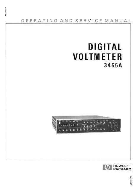
OPERATING AND SERVICE MANUAL<br />
MODEL 3455A<br />
<strong>DIGITAL</strong> <strong>VOLTMETER</strong><br />
Serial Numben: 1622A00101 and Greater<br />
IMPORTANT NOTICE<br />
This loose leaf manual does not normally require a change sheet: All<br />
major change information has been integrated into the manual by<br />
page revision. In eases where only minor changes are muird. a<br />
change sheet may be supplied.<br />
If the Serial Number of your instrument is lower than the one on<br />
this title page, the manual contains revisions that do not applv to<br />
your instrument. Backdating information given in the manual adapts<br />
it to earlier instruments.<br />
Where practical, backdating information is integrated into the text,<br />
parts list and schematic diagrams. Backdating changes are denoted<br />
by a delta slgn. An open delta !A1 or lettared delta (AA) on a given<br />
page. refen to the cotreswndinp backdatrng note on that page,<br />
Backdating changes not integrated into the manual are denoted by<br />
a numlxred delta (Al 1 wh~ch refers to the corresponding change in<br />
the Backdating section (Sectron VSII.<br />
To help minimize the possibility of electricat fire or shock<br />
hazards, do not expose this instrument to rain of excesive<br />
moisture.<br />
Manad Part No. 03455-90003<br />
Microfiche Part No. 03455-90053<br />
@Copyright Hewlett-Packard Company I W6<br />
P.O. Box 301, Loveland, CoIorado, 80537 U.S.A.<br />
Printed: July 1979
MEWLET T<br />
PACKARD<br />
CERTIFICATION<br />
Hewlett-Packard Company certvies that this product met its published specifications at the rime of shipment from the<br />
factory. He wletr-Packard further cerrgies that its calibrcrtion measurements are rmceeble ro the United States Na-<br />
tional Bureau of Standards. lo the exrent allowed by the Bureau's colibrarion facility, ond to the calibration facilities<br />
of other international Standards Orgunirarion members.<br />
WARRANTY<br />
This Htwlat-Paekard product is warranted against defects in material and workmanship for a period of one year<br />
from date of shipment [,txcept that in the case of certain components listed in Section I of this manual, the warranty<br />
shall be for the specified period] . During the warranty period, Hewletz-Packard Company will, at its option, either<br />
repair w replace products which prove to be defective.<br />
For warranty service or repair, this product must be returned to a service facility designated by -hp-. Buyer shall<br />
prepay shipping charges to -hp- and -hp- shall pay shipping charges to raurn the product to Buyer. However, Buyer<br />
shall pay all shipping charges, duties, and taxes for products returned to -hp- from another country,<br />
Hewlctt-Packatd warrants that its software and firmware designated by -hp- for use with an instrument will execute its<br />
programming instructions when properly installed on that instrument. Mtwlett-Packard does not warrant that the<br />
operation of the instrument, or software, or firmware will be uninterrupted or error free.<br />
LIMITATION OF WARRANTY<br />
The foregoing warranty shall not apply to defects resulting from improper or inadequate maintenance by Buyer,<br />
Buytr-supplied software or interfacing, unauthorized modification or misuse, operation outside of the environmental<br />
specificat ions for the product, or improper site preparation or maintenance.<br />
NO OTHER WARRANTY IS EXPRESSED OR IMPLIED. HEWLETT-PACKARD SPECIFlCALLY<br />
DISCLAIMS THE IMPLIED WARRANTIES OF MERCHANTABILITY AND FITNESS FOR A PARTICULAR<br />
PURPOSE.<br />
EXCLUSIVE REMEDIES<br />
THE REMEDIES PROVIDED HEREIN ARE BUYER'S SOLE AND EXCLUSIVE REMEDIES. HEWLETT-<br />
PACKARD SHALL NOT BE LIABLE FOR ANY DIRECT, INDIRECT, SPECIAL, INCIDENTAL, OR CONSE-<br />
QUENTIAL DAMAGES, WHETHER BASED ON CONTRACT, TORT, OR ANY OTHER LEGAL THEORY.<br />
ASSISTANCE<br />
Product maintenance ogreemenis and other customer assistance agreements are available<br />
for Hewlert-Packard products.<br />
For any assisrancc, conract your nearest He wlet t-Packard Sales and Service Office.<br />
add^^ are provided at the back of this manua!.
Pa HEWLETT<br />
PACKARD<br />
SAFETY SUMMkRY<br />
T h folluwhg ufrtl pmlltima murt k obwrwd during rll phwr of apsntien, dm, mild mpdr of tAh<br />
inltrumsnt Rilun ro comply with them prsclutions or with spsleific worninga elmwhen in thi8 manual violatus<br />
mfety mndmrda of hige, mmlnufmtturs, md intended uw of ths instrument Hswlstt-Pmekard Compeny assumen no<br />
linbility for the ewlnmm'r failure to comply with the88 rspuirsmsnt~. This is s Safety Class 1 imtrurnsat.<br />
GAOUlD THE IlltTRUMEllT<br />
To minimize shock hazard, the instrument chassis and cabinet must be connected to an elec-<br />
trical ground. The instrument is equipped with a three-conductor ac power cable. The power<br />
cable must either be plugged into an approved three-contact electrical outlet or used with a<br />
three-contact to two-contact adapter with the grounding wire {green) firmly connected to an<br />
electrical ground (safety ground) at the power outlet. The power jack and mating plug of the<br />
power cable meet International Electrotechnical Commission IIEC) safety standards.<br />
DO NOT OPERATE IR All EXPLOSIVE ATMOSPHERE<br />
Do not operate the instrument in the presence of ffamrnabl~ gases or fumes. Operation of any<br />
electrical instrument in such an environment constitutes a definite safety hazard.<br />
KEEP AWAY FROM LIVE CIRCUITS<br />
Operating personnel must not remove instrument covers. Component replacement and internal<br />
adjustments must be made by qualified maintenance personnel. Do not replace components<br />
with power cable connected. Under certain conditions, dangerous voltages may exist even with<br />
the power cable removed. To avoid injuries, always disconnect power and discharge circuits<br />
before touching them.<br />
DO NOT SERWCL OR ADJUST ALONE<br />
Do not attempt internal service or adjustment unless another person, capable of rendering first<br />
aid and resuscitation, is present.<br />
Because of the danger of introducing additional hazards, do not install substitute parts or per-<br />
form any unauthorized modification to the instrument, Return the instrument to a Hewlett-<br />
Packard Sales and Service Office for service and repair to ensure that safety features are main-<br />
tained.<br />
DANGEROUS PROCEDURE WARllllllGS<br />
Warnings, such as the example below, precede patentially dangerous procedures throughout<br />
this manual. Instructions contained in the warnings must be followed.<br />
I WARNING )<br />
Dm~rora<br />
voltmpw, mpnbls of causing death, Ire pmnt in thb inrtrumsnt Uw ex-<br />
tmma mutian whms hsndling, bslting, and adjusting
I<br />
I<br />
SAFETY SYMBOLS<br />
Genaral Definitions af Safety Symbols Used On Equipment or In Manuab.<br />
Instruction manual symbol: the product will be marked with this<br />
symbol when it is necessary for the user to refer ro the instruction<br />
manual En order to protect against damage to the instrument.<br />
Indicates dangerous voltage (terminals fed from the interior by<br />
voltage exceeding 1OOO volts must be so marked).<br />
Protective conductor terminal. For protcctisn against electrical<br />
shock in case of a fault. Used with field wiring terminals to in-<br />
- dicate the terminal which must be connected to ground before<br />
operating equipment.<br />
/f7 OR<br />
-<br />
Low-noise or noiseless, clean ground (earth) terminal. Used for a<br />
signal common, as well as providing prokction against electrical<br />
shock in case of a fault. A terminal marked with this symbol must<br />
be connected to ground in the manner described in the installation<br />
(operating) manual, and before operating the equipment.<br />
Frame or chassis terminal. A connection to the frame (chassis) of<br />
the equipment which normally includes all exposed metal structures.<br />
Alternating current (power line).<br />
--- Direct current (power line).<br />
Alternating or direct current (power line).<br />
The WARNING sign denotes a hazard. It calls attention to a pro-<br />
cedure, practice, condition or the like, which, if not correctly per-<br />
formed or adhered to, could result in injury or death to personnel.<br />
The CAUTION sign denotes a hazard. 11 calls attention to an<br />
CAVT'QN<br />
operating procedure, practice, condif ion or the like, which,if nor<br />
correctly performed or adhered to, could result in damage to or<br />
destruction of part or all of the product.<br />
' : The NOTE sign denotes important information. It calls attention<br />
to procedure, practice, condition oi the like, which is essential to<br />
highlight.
Model 3455A<br />
1-2, This Operating and &Senrice Manual contains informa-<br />
tion necessary to install, operate, test. adjust, and service<br />
the Hewlett-Paekard Model 3455A Digital Voltmeter.<br />
1-3. Included with this manual is an Operating information<br />
supplement. The supplement is a duplication of the first<br />
three sections of this manual and should be kept with the<br />
instrument for use by the operator.<br />
14. This section of the manual contains the performance<br />
specifications and general operating characteristics of the<br />
3455~, Also listed aw available options and accessories,<br />
and instrument and manual identification infonation.<br />
1.8. Instrument identification by serial number i s Iocated<br />
on the rear panel. Hewlett-Packard uses r two-section serial<br />
number consisting of a four-digit prefix and a fivedigit<br />
suffm separated by a letter designating the country in<br />
which the instrument was manufactured. (A = U.S.A.;<br />
G = West Germany; J = Japan; U = United Kingdom.) The<br />
prefuc is the same for all identical instruments and changes<br />
onIy when a major instrument change is made. The suffix,<br />
however, is assigned sequentidly and is unique to each<br />
instrument.<br />
1-9. This manual applies to instruments with serial num-<br />
bers indicated an the title page. If changes have been made<br />
in the instrument since this manual was printed, a yellow<br />
"Manual Changes" supplement supplied with the manual<br />
will define these changes and explain how to adapt the<br />
manual to the newer instruments. In addition, backdating<br />
information contained in Section V11 adapts the manual to<br />
instruments with serial numbers lower than those listed on<br />
the title page.<br />
1-10. hrt numbers for the manual and the microfiche<br />
copy of the manual arc also listed on the title page.<br />
1.1 1. D ESCR lPTlO l.<br />
1-12. The Model 3455A Digital Voltmeter makes ac volt-<br />
SECTION I<br />
Section I<br />
age measurements with five digit resolution and dc voltage<br />
and resistance measurements with 5 or 6 digit resolution as<br />
programmed by the user. The 3455A employs an automatic<br />
calibration (AUTO CALI feature which automatically cor-<br />
rects for possible gain and offset erron in the andog cir-<br />
cuitry to provide maximum accuracy. A remavable refer-<br />
ence module permits external calibration of the dc voltage<br />
and resistance functions. The reference module can be<br />
removed, calibrated and returned to the instrument, or the<br />
module can be replaced with another recently calibrated.<br />
reference. A MATH feature permits voItage or resistance<br />
measurements to be scaled into convenient units or to be<br />
read directly in percent enor from a selected recerence.<br />
The 3455A is HPdB proflmrnabIe for system applications.<br />
HP-=IB is Havlett-Pockoml 's implementation of<br />
1-5. SPE CI F I CATIO 'NS.<br />
IEEE std 488- 19 75, "'srond(~rd digitaI interface<br />
Id. Operating specifications for the 3455A are listed in for pmgrammobIe imfmmentation ':<br />
Tabk 1-1. These specifications are the performance standards<br />
or limits again. which the inarumcnt is tested. Table 1-13. O ~ ~ O N S<br />
1-2 lists general operating characteristics of the instrument.<br />
These characteristics are not specifications but are typical The options are available u+ with the<br />
operating characteristics included as additional information<br />
Model 3455A3<br />
for the user. Option 00 1: Average Responding AC Converter<br />
Option 907: Front Handle Kit<br />
1.7, IISTRUMENT AND MANUAL IDENTIFICATION. Option 908: Rack Mounting Kit<br />
Option 909: Front Handle and Rack Mounting Kit<br />
Option 9 10: Additional Set of Operating Information<br />
and Operating and Service Manuals<br />
1 - t 5. Accsasorias Supplied.<br />
1-16. A senice kit (-hp- Part No. 03455-8441 1) consisting<br />
of a PC extender board and a fuse is supplied with the<br />
Model J455A.<br />
1-17. ACCESSORIES AVAILABLE.<br />
1- 18. The following is a list of accessories available for use<br />
with the Model 3455A<br />
Accessory No. 1 Description<br />
-<br />
I1 177A<br />
3411tA<br />
I063 1 A<br />
106318<br />
I063IC<br />
03455-6 1609<br />
3455A Reference Module<br />
High Voltage Probe (40 kV dc)<br />
HP-IB Cable 1 meter 139.37 in.)<br />
IP-IB Cable 2 meter (78.74 in.)<br />
HP-IB Cable 4 meter (1 57.48 in.)<br />
Inguatd/Outguard Service Cable<br />
1-19. Recommended Test Equipmsmt.<br />
1-20. Equipment required to maintain the Model 345SA is<br />
listed in Table 1-3. Other equipment may be substituted if<br />
it meets the requirements listed in the table.
Section I Model 3455A<br />
Table 1-1. -if ieations.<br />
DC Voltage<br />
Specifications apply with Auto-Cal ON<br />
mmxtram<br />
&.a#mm: DImplav: km.cg: (I digir = JWI% of range)<br />
High High High High<br />
Resolution Resolution Resolution RexlluHon<br />
Off On Off On<br />
.TV - t.149999V -<br />
1V 1 Y 2 1.49994Y 5 1.49-V<br />
10V I0 V z 14.9999V z 14.99999V<br />
lmv IOOV ? 149.999V r 149 9999V<br />
lOOOV lOOOV 2 1000. OOV 2 1000. OOOV<br />
Rmw Srleetlon: Manual. Automatic, or Remote<br />
Performance (High Resolution Off)<br />
24 hours; 23°C % l°C<br />
10V mnge: % (0.002% of readng + 3 dl*)<br />
100 & lOOW mnge: -t1(0.004% of reading + 3 chits)<br />
1V range: * (0.003% of reading + 4 digits]<br />
90 days: 23°C ?SvC<br />
10V range: -. (0 005% of teading + 3 dglk)<br />
100 & lOOOV range.: +{0.007% of reading + 3 digits)<br />
1V range: *.(O.M)6% of reading + 4 digits)<br />
6 months: 23°C 25°C<br />
10V range: ?(0.008% of reading + 3 digits)<br />
100 & 10WV mnge: r (0.01 0% of reading + 3 drgts)<br />
1V mnge: 2 tO.M39% of reading +- 5 digts)<br />
tmrp8rmture CaafCicler#: [PC to 51PC)<br />
O.IV range: -t(O.lXK)3% of readlng + 0.15<br />
drgi&S/"C<br />
1 year. 23°C 2 5°C<br />
1QV range: ? (0.013% of reading + 3 digits)<br />
100 & lOOOV range: =(0.015% d reading + 3 digits)<br />
1V range: +(0.024% of reading + 6 dlgts)<br />
1V range: z [0.0003% of reading + 0.015<br />
digits)/"C<br />
1OV mnge: z (0.00015% of reading + 0.01 Input Characteristics<br />
digitslIoC<br />
100 & lOOOV range: = [O.MK)39& ot readfng + .01<br />
digits)/"C<br />
Accnrmw (1 digit = .001% of range):<br />
24 hours; 23°C 2 1°C<br />
1 QV range: * (0.002 W of readlng + 1 digit)<br />
1V range: 2 (0.003% ol reading + 1 digit)<br />
0.1Y range: =(0.004% of reading + 4 digits)<br />
100 & lMH3V range: = (0.004% d reading + 1 d~git)<br />
tmpu* haErt.nea:<br />
0.lV through 10V range: >lQm ohms<br />
lOOV and lOOOV range: 10 megohm %0.1%<br />
[with Auto-Cal OFF)<br />
Mufrnm Emput blt.ae:<br />
High to Low Input Terminals: *1000V peak<br />
Guard to Chassis: * 500V peak<br />
Guard to Low Terminal: +200V peak<br />
W days; 23'C 25°C<br />
10V range; ? (0.005% of readlng + 1 d@t)<br />
1V range: ?(0.006% of reading -i- 1 d~git)<br />
0.1V range: t (0.007% of reading + 4 digits)<br />
100 & 1WV range: * [O 007% of reading + 1 dig111<br />
1Yorr.E Mode ReJectioa (WIWR): NMR is the ratio of the<br />
peak normal-mode voltage to the peak error voltage in<br />
the reading.<br />
50 Hz optration: > 60 dB at 50 Hz * 0.1%<br />
60 Hz operalion: > 60 dB a1 M) Hz 2 0.1 WO<br />
6 months: 23°C t 5°C<br />
10V range: + (0.008% of reading + 1 diglt)<br />
Effectbat Com=on Mode RejecUon (ECMR): ECMR<br />
is the ratio of the peak common-mode voliage to the<br />
IV range: ? (0.009% of reading + 1 digit]<br />
resulrant peak error voltage in the reading with 1 kfl un-<br />
O.lY range: 2 (0.010% of reading + 5 digits)<br />
100 & FOOOV range: *(O 010% of read~ng + 1 dlgt)<br />
balancc in low lead.<br />
AC Inpui:<br />
I year, 23°C 15°C<br />
IOV mnge: =(0.013% of reading + 1 digit)<br />
IY range: 2 (0.014% of reading + 1 digit)<br />
O.1V range: =I0.015% of reading + 6 digits)<br />
100 & lOMlV range: (0.015% of read~ng + 1 digt )<br />
50 Hz opwation: > 160 dB at SO Hz k 0. I %<br />
60 Hz operation: > 160 dB at 60 Hz 0.1 %<br />
DC Input:<br />
> ladB<br />
~ ~ ~ ~ d ~ I d ~ l ~ ~ , ~ : =<br />
Performance (High Resolution On)<br />
64% 6ate h # b<br />
Ibolmtfmm B#olatlom<br />
toMl 5 readlngslsec. 3 readingslsec.<br />
Lto-oh !24 readlngsisec. 6 madingslsec.<br />
mlk mt. Im*<br />
Terpmmtmm Cwtticknb (WC to 50°C)<br />
1 V range: 2 (0.0003% of reading + 0.15<br />
digits)/"C<br />
IOV range: z (0.00015% of reading + 6.1<br />
Ruolwtlon Rmsolatllom<br />
digits)/"C<br />
100. & l w V range: 2 (0.0003% of reading + 0.1<br />
digitsI/"C<br />
5 readingslwc.
Model 3455A Section I<br />
Table 1-1. Specifications (Cont"d1.<br />
Ohms<br />
MaxImrm<br />
hn-: Dlmplmy: Accmep: 4 wlre k ohms* (1 digit = .00016'o of range)<br />
High High High mh 24 hours: 23°C t l'C<br />
Resolution Resolution Resolution Rexllution IkR range: =(0.0025% of reading -+ 4 digits)<br />
Off On Off On lOkIl range: 2 I0 M)45% of reading + 4 dig&)<br />
lOOkR rangem 1(0.0020% of reading +- 5 digits)<br />
.I kfl<br />
.14mkn -<br />
1000k12 range: -~(0.0120% of reading + 4 diqts)<br />
lkfl lkfl 1.49999kR 1.499999kfl<br />
10,aXlkfl range: (0. IOOQ% of reading + 4 digits)<br />
10 kR 10 kn 14.9Wkl1 14.99999kfl<br />
200kR lWkR 149 999kll 149.9999kR<br />
90 days; 23°C 25°C<br />
IOOOkR lOOOkR 1499 99k11 1499.999kR I kR range: * (0 0035% of reading + 5 digits)<br />
1OOMkR lM300kfl 14M 9k11 14999.99kil 1 OkR range: 2(0.0060'% of reading + 5 digits)<br />
100k12 range: +(0.0035% of reading + 6 digjts)<br />
Bmrsm 9.leemlol: Manual, Automatic, or Remote<br />
100akIl range: %(0.0135% of reading -t 5 d~glts)<br />
10,000kfl range: ?(0.1000% of reading + 5 d~gts)<br />
FmncCloa SIIdon: 2 wire k ohms w 4 wlre k ohms<br />
6 months; 23°C *5"C<br />
Performance (High Resolution Off)<br />
Tmrpnrtwe Codidark (0°C to 50°C)<br />
0.1 klk range. (0.0003% of reading + 0 2<br />
dlgiklloC<br />
1, 10 and lQQkR range: (0.0003% of reading + 002<br />
dlQitsl/"C<br />
la00kfl mnge: I0 TXX153h of reading * 0.02<br />
digits)/T<br />
10.000kR range: (0 004% of reading + 0.02<br />
dlgits)/C<br />
Acmm- 4 wire k ohms* t I digit = .MI4 of range]<br />
24 hours: 23'C f l'C<br />
O.lkfl range: *(O.M)3% of reading + 4 digits)<br />
~kfl range: ?(0.0040% of reading -t. 6 digits)<br />
IOkR range: ~(0.0065% of reading + 6 digits)<br />
lOOkR rangem ?{0.0040% of reading + 7 digits]<br />
lOOOkfl range. %{0.0140% of reading -I. 6 dlglts)<br />
10,000kIl range: e(0.1000X of reading + 6 dlgitsl<br />
l year. 23OC 25OC<br />
1 kR range: k(O.OW5sh of reading + 7 digits)<br />
l0kll lange: 2 10.0070% of reading + 7 digits)<br />
100kfl mnge: 2 (0.0045% of reading -I- 8 dqts)<br />
1000kIl range: + 10,0145% of reading + 3 dlglts)<br />
10,000kll range: 2 [0.100073 of readlng + 7 d~grts)<br />
*Atemncyr. 2 wire k ohms<br />
All accuracy specihcations are the same as 4 wire k ohms ex-<br />
,,pt 0 . ~ 4to k ~ readings,<br />
lkfl range: lr(0.0039 of reading + 1 digit)<br />
lOkR range: +.(0.005% of reading + 2 diyts) lnpllt characteristics<br />
wmhem #mmaf.td amom<br />
lOakfl range: ?(1).002% of reading + 2 dig~ts)<br />
lOOOki1 range: 2[0.012'% of readlng + 5 dlgrts)<br />
10.000kil range: ~(0.1% of reading + 5 digits)<br />
90 days; 23°C ?5T<br />
0.1 kfl range: *(0.005% of readlng + 5 digits)<br />
1 kR range: *(0.005% of rea$ing + I digit)<br />
IOkll range: + (0.007% of reading + 2 digits)<br />
100kfl range: ~(0.004% of reading + 2 digits)<br />
1000kIl range: k(0.0145 of reading + 5 dig~ts)<br />
1O.MXIkll range: =(0.100% oof readmg + 5 digits)<br />
6 months: 23T zS"C<br />
0.1 kil range: + (0.005% of reading + 6 digltsl<br />
1 kft range: z (0.0059; of reading + I digit)<br />
l0kll range: 2{0.007% d reading + 2 digrts)<br />
100kf1: range: ?(Q 004% of readtng + 3 dlglts)<br />
1000kIl range: %{Q.OI4'% of read~ng + 5 d~gts)<br />
10,000k11 range: ?(O. IOO% of reading + 5 dig~trl<br />
1 year; 23°C t5C<br />
0.1 kn range: c(Q.006% of reading + 7 digits)<br />
lkfl range: ~(0.006% of reading + 2 digits)<br />
loif1 range: =(0.008% of reading + 3 dtgits)<br />
100kfl range: 2(Q.005T9 of reading + 4 d~gits)<br />
1000kfl range: +(0.015% of reading + 6 dlgitsl<br />
10.000k11 range: *(0 100% of reading + 6 digits1<br />
Hm~ammm<br />
unknown:<br />
< 5 volts for oope circuit<br />
~4.7 volts for valid readlng<br />
-"I Dtl*q ~'omimm'):<br />
Olkfl. 1kO<br />
.d:D
Section I Model 3455A<br />
Ill.rlmrm<br />
hW-I D8oplay:<br />
High Rewlution High Resolution<br />
On or Off On or Off<br />
1V 1 . 4 ~ ~<br />
10V 14.9993V<br />
lOOV 149.999V<br />
IOOOV 1090 OOQ<br />
R.e#m SIIacUor: Manual. Automatic. or Remote<br />
Fumedon Saketiom: ACV or Fasf ACV<br />
Table 1-1. Specifications (Cont'dl.<br />
AC Voltage (RMS converter)<br />
Performance<br />
Jemptr.tum CorCficlest: (0°C to 50°C) for inputs 1W of full scale: 2(0.002% of reading + 2 dlglh)/T<br />
AC coupled. input < 156 of full scale: 002% of reading + b digits)/"C<br />
AC/DC coupled. ~(0.002% of teadlng * 6 dIgitsl/'C<br />
Aoeurmcy: % of reading + digits or (96 of range) I' IAC Coupling)'<br />
FASIT ACV. SblHr-2OkH+ tlkwx- Il@kHr IHkWr-2 SOkH.' 251kHz-SOOLHf SMkUm IMh'<br />
ACV' SOH.*Z,kHa 20kHs.100kHz I WkHr-250kHau 251kHz-5~OhHzo 500kH1-1 MH+'<br />
I4 bra: 2S"C z 1°C<br />
amp.; ZS°C * ST<br />
L ran: XS'C zS°C<br />
I ymmt: 03°C 15°C<br />
~rdmuub.~ommndlubu 'FmwAC IXrarWudlwd . d d r D * r . d h r Zn4nlm,borwrwur1* rrv<br />
%r#h.lm+ m mAr h :WE k.* imn I* ol r a p la*mnRCtKcnuCirdmmi.bor'diVlru*l '~;dha~.r.Wlm~n~~rbrrr~tur-~Wb*<br />
FwAl
Model 3455A Section I<br />
Mmxi~mm<br />
B.m#me: Wmplny:<br />
Table f -1. Specifications (Cont'dl.<br />
AC Voltage (Average Converter Opt. 001)<br />
High Redutlon High Resolution<br />
On or Off On or Off<br />
IV 1.49999V<br />
10V 14.9999V<br />
lOOV 149.999V<br />
1OOOV 1oOo.00v<br />
hrgr Slketlom: Manual, Automatic, or Remote<br />
FaactCor &l*cBor: ACV or Fast ACV<br />
Performance<br />
krmmtrm Corffidant: (WC to 5PC)<br />
-1 (0.WZx of reading + 2 digits)/'C<br />
Aeemey: 5 [% of reading + digits or (% of range) ] l<br />
FAST ACV' WIk5WtL 5WlhlhHr ILMx-lWkh l~H+-tSW<br />
ACV~ 30HpWH+ 56Hr~iOQll. 1a).lt-1WkH. 1Wklt*251kW<br />
24 h.: 53% ?1'C<br />
Wd.gm:XSOC=SOC<br />
6 mom: 2ST ?ST<br />
1 r.: 2ST 28°C<br />
Input Characteristics<br />
0.47% + 70 dlg.<br />
(.07%)<br />
0 32% + 50 Mg.<br />
t.mW<br />
0,35%+50drg,<br />
'G,."lmuab.dsrta.<br />
(kIk1Wrmp .dd001p~nluoll-kI+<br />
Sprrh.r-nh me lor nw kwh m b a * 1 IIW d rangr<br />
' T r m w v l pu,~ 1h.n ImMr~abda I ud 1W d y<br />
Acrurrr n nm .prllld d 7 h r mrk k r l l pmdwt 111'<br />
lmpmt 1-pmdmnca:<br />
Front Terminals-2Mll= 1% shunted by less than l@F<br />
Rear Terminals-PMflz 1% shunted by less than 75pS<br />
Marlmum Impml Uoltanr:<br />
High to Law Terminals: * 1414 volts peak (Subject to a<br />
voll - Hz limitation)<br />
Guard to Chassis: 2500Y peak<br />
Guard to Low Terminal: 2200V peak<br />
imam Remdlmg ate:<br />
mH. Oat. t.ytL IIH. ate W L<br />
RU~OIH TI-:<br />
ACV and FAST ACV<br />
First reading to 4.1% of step size when Mggered coincj-<br />
dent with step change when on correct range<br />
(for AC signals with no DC componenf)<br />
0 09% + 25 dl9<br />
{.M5%)<br />
0 70% + M1 dig<br />
OSQ%+70dig<br />
( 07%)<br />
(.05051<br />
0.1% +25d1g.<br />
f.M5%1<br />
106%)<br />
0.75% + 60 d~g<br />
tm%I<br />
0.50% + 70 dig. 0.40% + 60 dig 0.1% + 30 dig. 0.75% + 70 dlg.<br />
1.07~)<br />
0.50% + 70 dig.<br />
(.~%i (.Q3%1<br />
0.40% + 70 dig. 0.12% + 35 dig.<br />
(.a7t9)<br />
0.75% + 80 dlg.<br />
t.M%l / @%I<br />
1.1 read~ngslsec. 12 readw~gslwc.
Section I Model 34556<br />
1-6<br />
Table 1-1. Specifications (Cant'd ).<br />
Math<br />
% E m X-Y 100%<br />
(.><br />
X Is present reading. Y and Z are previously entered read- X Is present reading. Y is a previously entered reading, or<br />
ing. numbementered from the front panel armluesentered number entered from the front panel or by external program.<br />
by external program.<br />
Mm~lmrr Nrrh (Entered or Displayed)<br />
~mnlrrr Nrrbn: (Entered or Displayed) -c 199.999 9<br />
-. 199.999 9<br />
Accrrmqey:<br />
Accnncgi *(ACCURACY OF X READING t 1 DIGIf OF DIS.<br />
-(ACCURACY OF X READING r l DIGIT OF DIS- PLAYED ANSWER)'<br />
PLAYED ANSWER)'<br />
'This assumes no "Y' emr.<br />
'This assumes no "Y' or "F' emr.<br />
Raw %-Ion: Mnrsl. Automk, or Asme<br />
Function Clmlon:<br />
DC Vdts<br />
AC Voltr (ACV w FAST ACV)<br />
OHMS (2 wlr* kllohm or 4 wlrr kllohml<br />
TEST<br />
MDRMAL MODE RWECTION (50 Hz DPERATIOFIJ<br />
racoutlucriwrr<br />
fable 1-2. Typical Oprrtting Charwteristlcs.<br />
Effmiw Noh kndwldth<br />
T - 1 IBO mc for 5 &@it 6tF Hz Operation<br />
T - 2115 let for 6 digtt a] Hr Opsrntion<br />
T 1 EO rec for 5 digrt 60 Hz Owration<br />
T - 4/25 sec for 6 d8grt 50 Hz Operation<br />
COMMON MODE REJECTION 11 KILOHM IMBALANCE)<br />
,%3<br />
9-<br />
1m<br />
=<br />
Y 'W<br />
5<br />
2 $70<br />
NORHA EFFECTIVE C<br />
m urn<br />
M 14<br />
W !m<br />
rn<br />
1; " - 150<br />
2<br />
* m<br />
10<br />
I0<br />
0<br />
P REUurwY ,HI!<br />
Nwml Mode Rajmion a M log 1 - ::if T 1<br />
im<br />
PO<br />
w<br />
I<br />
2 rta<br />
+<br />
U w<br />
: 1 9<br />
110<br />
111<br />
I 10 I w<br />
r *r~UtkCr IM,I<br />
1<br />
i<br />
I
Model 3455A Section I<br />
EFFECTIVE COMMON MODE REJECTION (60 Mz OPERATIOW)<br />
urn<br />
Typicsl HP-I8 Handshake Tim:<br />
Ac~ept Data - (3455A addre- to lirten or ATN true)<br />
500 ~ sec per character typical (0 delay sourel<br />
Output Oeta - (3455R ddrwsed to tatkl<br />
250 pwc per chsracfar typld (0 delay acceptor1<br />
1-21, SAFETY COtrlSIOERATlQNS.<br />
1-22. The 3455A is a safety class 1 instrument (provided<br />
with a protecrive earth terminal j. The instrument and man-<br />
ua! should bc reviewed for safety symbols and instructions<br />
before operation.<br />
Table 1-2. Typical Operating Charactwristi~ {Cont'dl.<br />
General (Auto Cat must be on fw 75 seconds to meet 811<br />
specifiwtionsl<br />
Overload Indication: OL<br />
Operating Temperature: O'C to 50'~<br />
Warmup Time: One hour to meeiall spmifications<br />
Humidity Range: < 95% R6H., 0 C tg 40 C<br />
Storage Temperaturn: 40 C ta *75 C<br />
Power: 10011201240 V +5%. -10% 48 Hz to 4aE Hz Ilrm<br />
operation < 60 VA<br />
220 V + TO% 48 Hz 10 400 Hz line operation<br />
< 60 VA<br />
Dlmenslons: 88.9 mm hlgh x 425.5 mm wide x 527.1<br />
mm deep 13%" high x 16%" wide K 20%" deep)<br />
Weights: Net - 9 kg (21 Ibs.)<br />
Shipping - 12 kg (28 Ibs.)
Section 1 Model 3455A<br />
'<br />
Reference Divider<br />
DC Transfer Standard<br />
Electronic Counter<br />
Resistan~e Standard<br />
Bun System Anelyzm<br />
Celculator<br />
~eclllorcape<br />
Digital Voltmeter<br />
Reoistors<br />
Signature Analyzer<br />
Table 1-3. Recommended Test Equipment<br />
Division Ratio Accuracy + ,001 %<br />
Output Voltage Range - 1 Y to 1 kV<br />
Output Voltages: 1 Y. 1.018 V.<br />
1.01 9V. 10 V<br />
Accuracr: i 5 PPm<br />
Stabilitv: f -001 % (30 days)<br />
50 Hz to 60 Hz<br />
Resistance: 1 kf2<br />
Accuracy: + .MK)S%<br />
Resistance: 100 K<br />
Accuracy: i .002%<br />
HP.1 E Control Capebllilv<br />
HP-I 8 Control ambiritv must<br />
serve as printer for 3455A<br />
Output data.<br />
Bandwidth: DC to 10 MHz<br />
Sweep 5me: 0.1 w to 1 secldiv<br />
Sensif ivity: 1 Vldlv<br />
Voltage Range: 10 mV to 1 OOO V<br />
Resolution: l0 pV<br />
1 Resistances:<br />
1 kn+lO%<br />
TO kR t 0.7 %<br />
1 Ma 20.1%<br />
P - Performance Checks T = Troubleshooting<br />
A = Adjustments 0 = Operators Check<br />
Fluke Model 750A<br />
Reference Divider<br />
Fluke Model 731 A<br />
DC Transfer Standard<br />
+hp Mo~el5300Ai5302A<br />
Messuring Sysrern<br />
Guildlne Model<br />
833011 K or 9330Al1 K<br />
Guildline Model 9330F100 K<br />
-h~- Model 59401 A<br />
Bus System AnslyzW<br />
+hp Mode1 9825A<br />
hp Model l8OCJD<br />
Otcilloscoge with<br />
1801 A and 18211 A<br />
plug-in unin<br />
-hp Model 3490A<br />
+hp Part No.<br />
0684-1 021<br />
06984357<br />
0698-6369<br />
-hp- Model 5004A<br />
I<br />
PA<br />
PA<br />
P<br />
A<br />
T<br />
OT<br />
T<br />
PAT<br />
P
Model 3455A<br />
2-2. This section contains information and inst ructions<br />
necessary to install and interface the Model 3455A Digital<br />
Voltmeter. Also included are initial inspection procedures,<br />
power and grounding requirements, environmental inforrna-<br />
tion, and repackaging instructions.<br />
2.3. INITIAL INSPECTION.<br />
24. This instrument was carefully inspected both rnechan-<br />
icaliy and electrically before shipment. It should be free of<br />
mars and scratches and in perfect electrical order. The<br />
instrument should be inspected upon receipt for damage<br />
that might have occurred in transit. If the shipping con-<br />
tainer or cushioning material is damaged, it should be kept<br />
until the contents of the shipment have been checked for<br />
completeness and the instrument has been mechanicfly<br />
and etectricdly checked. Procedures for testing electrical<br />
performance of the 34S5A are given in Section IV. If the<br />
contents are incomplete, if there is mechanical damage or<br />
defect, or if the multimeter does not pass the Performance<br />
Tests, notify the nearest Hewlett-Packard Office. (A list of<br />
the -hp- Sales and Service Offices is presented at the back of<br />
the manual.) IF the shipping container is damaged, or the<br />
cushioning material shows signs of stress, notify the carrier<br />
as well as the Hewlett-Packard Office. Save the shipping<br />
materids for the carrier's inspection.<br />
2-5. PREPARATION FOR USE.<br />
2-6. Power Requirements.<br />
SECTION II<br />
2WW 4, Irn *"I<br />
rzo *IN* WvmI"<br />
TOO volts 90 to 105 volts<br />
120 volts 3 08 to 3 26 volts 0.5 A<br />
220 volts 198 to 231 volts 0.25 A<br />
240 vorrs 21 6 to 252 volts 0.25 A<br />
Figure 2-1. Lima Voltage Selection.<br />
Section 11<br />
used far -hp- power cables. The -hp- part numbcr directly<br />
below each drawing is rhe part number for a power cable<br />
equipped with a connector of that configuration. If the<br />
appropriate power cable is not included with the instru-<br />
ment, notify the nearest -hp- Safes and Service OFfice and<br />
the proper cable will be provided.<br />
2-12. Grounding Requirernsnrs.<br />
2-1 3. To protect operating personnel, the Nat ienal Electri-<br />
cal Manufacturer's Association (NEMA) recommends that<br />
the instrument panel and cabinet be grounded. The Model<br />
3455A is equipped with a three conductor power cable<br />
which, when plugged into an appropriate receptacle,<br />
grounds the instrument.<br />
2-7. The Model 3455A requires a power source of 100, 2-14. Bench Use.<br />
120.220, or 240 V ac (+ 56 - lo%), 48 Hz to 400 Hz single<br />
phase. Maximum power consumption js 60 Vd.<br />
2-1 5. The Model 3455A is shipped with plastic feet and tilt<br />
stands installed and is ready for use as a bench instrument.<br />
2-8. tine Voltage Selection.<br />
The plastic feet are shapcd to permit "stacking" with other<br />
2-9. Before connecting ac power to the 3455A, make sure<br />
the rear panel line selector switches are set to correspond to<br />
the voltage of the available power line as shown in Figure<br />
2-1. Also, be sure the proper Fuse Is installed. The multi-<br />
meter is shipped with the line voltage and fuse selected for<br />
120 V ac operation.<br />
Be sure the 50 - 60 Hz rear panel s~'tch is set<br />
for the proper line frequenq for your lecatiorr,<br />
2.1 0. Power Cable,<br />
2- 1 1. Figure 2-2 illustrates the standard configurations Figura 2-2. Power Cord Configurations.<br />
2- 1
Section I1 Model 3455A<br />
full-module Hewlett-Packard instruments. The tilt stands<br />
permit the operator to elevate the front pane[ far operating<br />
and viewing convenience.<br />
2-1 6. Rack Mounting.<br />
2-17. The Modd 3455A may be rack mounted by adding<br />
rack mounting kit Option 908 or Option 909. Option 908<br />
contains the basic hardware and instructions for rack<br />
mounting; Option 909 adds front handles to the basic rack<br />
mount kit. The rack mount kits are designed to permit<br />
the Multimeter to be installed in a standard 19 inch rack.<br />
When rack mounting, additional support must be provided<br />
at the rear of the instrument. Be sure that the air intake at<br />
the rear of the instrument is unobstructed.<br />
2-18. Ihterfgcs Connections.<br />
2-19. The Mode1 3455A is compatible with the Hewlett-<br />
Packard Interface Bus (HP-IIB).<br />
NOTE<br />
HP-lB is Havlert-Packad 3- implementation of<br />
lEEE std 488-19 75, 'Standard Digito I Interface<br />
for fiogrurn~nrrble Insrnimenrarion ".<br />
The Multirncttr is connected to the HP-IB by connecting an<br />
HP-IB interface cable to the 24-pin connector Iocated on<br />
the rear panel. Figure 2-3 illustrates typical HP-IB system<br />
interconnections and shows the 1063 1 AJBJC HP-IB Inter-<br />
face Cable connectors. Each end of the cable has both a<br />
male and female connector to simplily intcrconnection of<br />
instruments and cablcs. As many as 15 instruments can be<br />
connected by the same interface bus; however. the maxi-<br />
mum length of cable that can be used to connect a group of<br />
2-2<br />
instruments must not exceed 2 meters (4.5 ft.) times the<br />
number of instruments to be connected, or 20 meters<br />
(65.6 ft.), whichever is less.<br />
2-20. Address Selection. The HP-IB address switch,<br />
located on the rear panel, permits the user to set the "talk"<br />
and "listen" address of the instrument. The talk and listen<br />
address is a 7-bit code which is selected to provide a unique<br />
address for each bus instrument. The 3455A normally<br />
leaves the factory with the address switch set to a "Listen"<br />
address of 6 and a "talk'hddress of V. The address switch<br />
also allows selection of a "talk-only" mode. Refer to<br />
Paragraph 3-42 for address selection instructions.<br />
2-21. External Trigger. A BNC connector, located on the<br />
tear panel, is provided for an external trigger input. The<br />
trigger input is to be driven with TTL level signals.<br />
2-22. ENVIRONMENTAL REQUIREMENTS.<br />
piiq<br />
To prevent eiectricol shock or fire hazard, do<br />
not expose the instrurnent ro soin or moisture.<br />
2-23. Operating aad Storage Temperature.<br />
Figure 2-3. Typical HP-I5 Synem Intereonnectiona.<br />
2-24. In order to meet the specifications listed in Table<br />
1-1, the instrument should be operated within an ambient<br />
temperature range of 23°C * 5OC (73°F 2 9°F). Tht inslmmen<br />
t may be operated within an ambient temperature<br />
range of O"C to + 55"~ (+ 32°F to + 13 1 OF) with degraded<br />
accuracy.<br />
2-25. The instrument may be stored or shipped where the<br />
ambient temperature range is within 4 0 ' ~ to +75'~<br />
(40°F to + 1 6J°F). However, the instrument should not
e stored or shipped where temperature fluctuations cause<br />
condensation within the instrument.<br />
2-26. Humidity.<br />
2-27. The instrument may be operated in environments<br />
with relative humidity of up to 95%. However, the instru-<br />
ment must be protected from temperature extremes which<br />
cause condensation within the instrument.<br />
2-28. Attitude,<br />
2-29. The instrument may be operated at altitudes up to<br />
4572 meters ( 1 5,000 feet).<br />
2-30. REPACKAGING FOR SHIPMENT.<br />
Nrn<br />
If the insmment is ro be shipped to Hewleft-<br />
Packard for service or repair, attach a rag to the<br />
instrument Edenrifying rite owner and indicating<br />
the sewice or repair to be accompiished.<br />
Include rhe model number and full serial num-<br />
ber of rite instrument. In any correspondence,<br />
identrjy the instrument by model number and<br />
full serial number. If you have any questions,<br />
mntact your nearest -hp- Sales and Service<br />
Office.<br />
Section IE<br />
2-3 1. The following is a general guide for repackaging the<br />
instrument for shipment. If the original container is avail-<br />
able, place the instrument in the container with appropriate<br />
packing material and seal well with strong tape or metal<br />
bands. If the original container is not available. proceed as<br />
~olollows:<br />
a. Wrap instrument in heavy paper or plastic before<br />
placing in an inner con t ajner.<br />
6. Ptacc packing material around all sides of instrument<br />
and protect panel face with cardboard strips or plastic<br />
foam.<br />
c. Place instrument and inner container in a heavy<br />
carton and seal with strong tape or metal bands.<br />
d. Mark shipping container '"DELICATE IKSTRU-<br />
MENT", "'FRAGILE", etc.
Section III Model 3455A<br />
3-0<br />
HP-la* status indiceton: High Resolution switch - swttches display from 5.112<br />
located rn the center of the key indicates High ResoFu-<br />
tron on when lit.<br />
TALK - lights when the 3455A is addressed to "talk". Trigger Selection K~ys - permits setection of INTER.<br />
LOCAL switch - permits; the operator to return the<br />
Display - Indicates polarity and amplitude of the<br />
@ measurement. Measurement results are presented in either<br />
5-3 12 d~glto or 6-1 R digbts depend~ng upon whether the<br />
HIGH RESOLUTION feature 1s off or on. An LED rn the<br />
upper left corner of the display rndicates sample rate of<br />
the 3455.4 Five LEO'S. located to ihe right of the display.<br />
~nd~cate whether the display vs presenting DC Voltage,<br />
AC Voltage, Ohms, Scale or % error measurement<br />
results.<br />
Range Selection Keys - permit selection of ranges as<br />
DC vorts: .I V, 1 V, 10 V. IMI v. I kv. AUTO<br />
AC Volts. 7 V. 10 V. f OO V. 1 kV, AUTO<br />
Ohms: .I K, 1 K, 10 K, 100 K, 1.000 K, 10.000 K, AUTO<br />
LED'S located in the center of thp! keys indicate which<br />
range is selected.<br />
key has an LEO which lights to rndlcate the trrgqer source<br />
Sample Rere Centrots - permit selectcon of ma~imum<br />
@ sample rate ai the present sample rare diuidd by 2. The<br />
maximum sample rate may be dlvlded by 2 uo to 6 times<br />
for a minimum sample rate of: maximum sample rate<br />
1 @<br />
@<br />
Binary Program Indicator - indicates when the 3455A is<br />
operating in the Binary Program mode. Rafar ta<br />
Paragraph 3-66.<br />
Math Controls - Selen SCALE ( E l , % ERROR<br />
Y<br />
tw x 100). or MATH OFF. The Math feature selected<br />
Y<br />
is indicated by an LED located in the key (Paregraph<br />
3-1 91.<br />
Function Selection Keys - DC Volts. AC Volts, FAST<br />
@ AC Voltr.2WlREXn.4WlREkn.andTEST.LEO'r<br />
located rn the center of the keys ~ndlcate whlch funct~on<br />
IS selected.<br />
Auto Ca'l switch - allows the Auto-Cal feature to be turn-<br />
a ed on or off. LED in center of Key indicates Auto-CaI on.<br />
Refer to Paragraph 3-29.<br />
@<br />
@<br />
@<br />
ENTER controls - Recall the number stored in the Y or Z<br />
regis7.r 10 the display. also "shifts" the front .and<br />
keyboard to permit entry of new data to be stored in the<br />
Y or Z registers (Paragraph 3-23).<br />
STORE Controls - The Store controls transfar the<br />
number presently being displayed info the Y or Z register<br />
(Paragraph 3-23E.<br />
Rear Terminal Indicator - indicates when the rear input<br />
terminals have been selected.<br />
Figure 3-1. Front and Rear Panel Features.<br />
64<br />
1
Model 3455A Section III<br />
3-2. This section contains infomation and instructions<br />
necessary for operation of the Modtl 3455A Digital<br />
Voltmeter. Included is a description of operation<br />
characteristics, a description of the operating controls<br />
and indicators, and functional checks to be performed<br />
by the operator.<br />
3-3. OPEflATkllG CHARACTERISTICS.<br />
3-5. Befare connecting ac power to the 345519, make<br />
certain the rear panel lint selector switches are set to<br />
correspond to the voltage and frequency of the available<br />
power line and that the proper fuse is installed for the<br />
voltage selected. For rated measurement accuracy, the<br />
3455A should be aIlowed to warm up for at least one<br />
hour.<br />
SECTION Ill<br />
OPERATING INSTRUCTIONS<br />
logic of the instrument. When all these measurements<br />
and caSculations are compIeted. the 34S5A wilI display<br />
+ .8.8.8.8.8.8.8. and the self-test operation will start<br />
again. In order to bring the instrument out of this mode,<br />
any other function button must be pressed.<br />
3-8. En the event of a cal constant failure, the Self-Test<br />
operation will stop and the failing cal constant's number<br />
will be displayed (an integer number from 13 to 0). If<br />
the dummy calculation fails, a non integer number is<br />
displayed {e.g., 9.998 or 10.Mi2 etc.).<br />
3-9. The Self-Test function can be remotely programm-<br />
ed, as described in the programming portion of this sec-<br />
tion. The 3455A will output a 10 upon a succtssful com-<br />
pletion of the tat and if addressed to "talk." If the<br />
dummy calculation fails, the answer of the dummy<br />
calc~llation will be the output (9.998 or 10.002 etc.). If<br />
any auto-cal constants fail, the 3455A will not output<br />
any readings, (times out).<br />
3.6. s8R Tmt Opantlon. NOTE<br />
3-7. Thc internal test function of the 3455A verifies the The seCf test fmm does not test opemrion<br />
operation of the dc analog circuitry, inguard and of the ohms or ac sections nor the measure-<br />
outguard logic circuitry, and the front panel indicators ment amuracy of the 3455A.<br />
and display. The primary test of the dc analog circuitry<br />
is the measurement of various Auto-Cal constants. A 3-10, QC Yohqs Ma~rmtmt<br />
logic check is also performed, when all the cal constant<br />
measurements are taken. The logic check consists of a 3-1 1. The Model W55A measures dc voltagc from 1<br />
dummy cal constant calculation made in the outguard microvolt to 1OOO volts in five ranges extending from .1<br />
Ohms Slgnnl Terminals - supplims drhra signal fw<br />
4-WIRE Ohms measurements (Paragraph 3-1 21.<br />
Input Terminals<br />
GUAAO switch - Internally connects the Guard terminal<br />
to the LO Input terminal Ifor front panel opemtion only,<br />
Paragraph 3-41 1.<br />
GUARD Terminal<br />
Ohms Signal Terminals<br />
Input Terminals<br />
Guard Terminals<br />
REAR PANEL<br />
FrontlRear INPUT SELECT switch<br />
HP-IS" Connector - see Paragraph 2-1 8 and 3-48<br />
AC or AClOC Input Select~on sw~tch - refw to Paragraph<br />
5-14.<br />
Cine Frequency Selection Switch - must be set to cones<br />
pond to The power line frequency 450 Hz or 60 Hz).<br />
Reference Module<br />
EXTERNAL TRIGGER Input Connacror<br />
HP-IS" Address Sa!mtion Switch - mkr to Paragraph<br />
3-53.<br />
Cooling Fan<br />
Power Line Voltage Selection Switches - refer to Para-<br />
graph 2-8.<br />
Fuse - 90 W to 126 V - 0.5 amp. 198 V to 252 V -<br />
0.25 amp.<br />
AC Power Connector.<br />
Figure 3-1. Front and Rear Panel Features (Cont'd).<br />
"HP-1B IS Hewlett-Packard's implementation of IEEE Srd.<br />
488-1975. "Standard D~gital Interface for Programmable<br />
InstrumenTation".
Section I11 Model 34556<br />
4-WIRE MEASUREMENT 2-WIRE MEASUREMENT<br />
ilSIBNAL INWT GUARD nSlGNAt INPUT GUARD<br />
(4 WIRE) (2 W Ie)<br />
volt full-scale to 1OOO volts full-scale. Measurement<br />
results are presented in 5-I/2 digits during normal<br />
operation or in 6-1/2 digits when the 345% is set to the<br />
High Resolution mode. All ranges except the IOOO voIt<br />
range have 50% overrange capability and are overload<br />
gratected from input voltages up to ~tr 1 OOO volts. Input<br />
resistance in the dc function is greater than 101%ohms<br />
on the -1 V, 1 V, and 10 V ranges and equal to 10<br />
megohms on the 100 V and 1000 V ranges. Refer to<br />
Table 1-1 for DC Accuracy specifications.<br />
3-13. The Model 3455A measures resistance from 1<br />
milliohm to IS megohms in six ranges extending from .I<br />
kilohms ful scale to 10,000 kilohms full scale. Measure-<br />
ment results are presented in 5-1/2 digits during normal<br />
operation or in &1/2 digits when the 3455A is set to the<br />
High Resolution mode, The only exception is that the .I<br />
V range can only take a measurement in the 5-1/2 digit<br />
mode. Resistance may be measured in "CWIRE" con-<br />
figuration for optimum accuracy or "2-WIRE" eon-<br />
figuration may be selected for measurement conve-<br />
nience. Figure 3-2 shows proper connections for making<br />
resistance measurements, The nominal output signal<br />
current on the .1 kilohm, 1 kilohm and 100 kiIohrn<br />
ranges is .7 mA. The nominal output current on the<br />
1000 kilohm and 10,000 kilahm ranges is .7 microamp.<br />
Maximum output voltage is limited to less than 5 volts<br />
on all ranges. Refer to Table f -I for ohm accuracy<br />
specifications.<br />
Figure 3-2, Ohmmeter Meaw rement Connections.<br />
3455-8- 4667<br />
volts RMS. Readings taken in the ac function art<br />
display in the 5-1/2 digit mode only. Input impedance<br />
of both convertors is 2 rnegohms in parallel with<br />
< 75 pF for rear terminal input and < 90 pF for front<br />
terminal input. In addition to the normal ac voIts func-<br />
tion, the 3455A also has a fast ac volts function. The<br />
fast ac function has a faster ac reading rate than the nor-<br />
mal ac function.<br />
3-16. The frequency response of the true RMS conver-<br />
tor is from 30 Hz to 1 MHz in the normal ac volts func-<br />
tion and from 3QO Hz to 1 MHz in the fast ac volts func-<br />
tion. Both ac signals or ac plus dc signals (ac signals<br />
superimposed on a dc level) can bt measured by the true<br />
RMS convertor, Selection of the ac or ac + dc inputs<br />
are chosen by a switch Iccated behind the rear panels<br />
reference cover. Refer to Table 1-1 for accuracy<br />
specifications of each ac mode.<br />
3-17. The frequency response of the average converter<br />
is from 30 Hz to 250 Hz in the normal ac volts function<br />
and from 300 Hz to 250 kHz in the Fast ac voIts func-<br />
tion. Only ac signals (no dc component) can be<br />
measured by the average converter. Refer to Table 1-1<br />
for accuracy specification of each ac mode.<br />
3-18. In order to get accurate ac readings (especially<br />
with high voltage inputs at high frequencies), the low in-<br />
put terminaI (front and rear) should be connected to the<br />
guard terminal (front and rear). Refer to paragraph 3-39<br />
for guarding information.<br />
3-15. The -hp Model 3455A offers a choise of true<br />
RMS (standard unit) or average responding at: conver- NOTE<br />
tors (Option 001). Both methods measure ac voltages<br />
from 10 microvolts to 1000 volts in four ranges exten- The front pneI guard pushbutton appii~<br />
ding from I volt to 1000 volts ranges. AIE ranges, except only for front panel inputs. Be sure to wire<br />
the 1OOO volts range, have 50% overrange capability and rear panel guard connections yourself, V ifare<br />
protected from input voltage components up to 1000 ing the m r panel input terminals.
Model 3455A Section I11<br />
3-20. The math feature of th 3455A allows the measure-<br />
ment value to be offset and/or scaled by known values<br />
or to be expressed in percent of a reference value.<br />
3.21. Sale Mods. The scale mode of the math feature is<br />
described by the formula: result = X-Z where x is the<br />
Y<br />
measurement value, z is the offset value, and y is the<br />
scale factor. This mode allows the measurement value to<br />
be modified by the addition, subtraction, multiplication<br />
or division of a known value. Addition and subtraction<br />
are performed by entering the nurnber to be added or<br />
subtracted in "2" and entering 1 in "y". The scale for-<br />
muIa then becomes: result = x - (* d = x - ( f z).<br />
1<br />
Division is performed by entering 0 in "z'9ad the<br />
divisor value in "y." The scale formula then<br />
becomts: result = 5 -5 Multiplication is perform-<br />
Y Y<br />
performed by dividing the measurement value by the in-<br />
verse of the multipIier value; that is, multiplication is<br />
performed by dividing by a fraction. The scale formula<br />
becomes: result = . X - 0 = xy. As an example: to<br />
1 /Y<br />
multiply by 10, divide by the inverse of 10 which is 1/10<br />
or .I. Various examples using the scale mode are as<br />
follows:<br />
a. Current Measurement: Accurate current<br />
measurements can be made by using a low value resistor<br />
shunting the 3455A's input terminals. The value of the<br />
resistor is then entered in the '"y" register (see<br />
Paragraph 3-22), and zero is entered in the "z" register<br />
Wirh the resistor connected at the input terminal and the<br />
instrument set in the voltage mode, current<br />
measurements can now be made. You can do this by<br />
connecting the input across the resistor and measuring<br />
the voltage drop across the resistor. This voltage drop is<br />
proportional to the current through the resistor. By<br />
switching the 3455A to the scale mode, the reading<br />
becomes an accurate current reading in rnilliamps. Since<br />
the resistor value is in kiIo ohms (R) and stored in "y",<br />
and since zero is stored in "z". the scale equation<br />
becomes:<br />
v-0 v<br />
X'Y = - = -= current in rnilliamps<br />
Y R R<br />
where R = Resistor across the input terminaZs<br />
V = Voltage drop across the resistor<br />
b. Temperature Measurement: A temperature mea-<br />
surement can be made by using a line or resistive<br />
temperature sensor.<br />
Assume that the sensor has a resistance of 1 kiIohrn at<br />
25°C and changes 5900 ppm/"C. At 0'C the sensor<br />
would have a resistance of 852.5 ohm (1 kilohm - 15.9<br />
ohms) 25). This number is divided by 1000 since the<br />
3455A measurement results are expressed in kilohrn and<br />
is entered in the "2" register to remove the offset at<br />
0°C. The measurement result of the 3455A is scaled ?a<br />
read directly in degrees centigrade by solving the equa-<br />
tion for the value of "y". This is done where the results<br />
of the equation are equal to 25°C since the sensor<br />
resistance is specified at that temperature. The scale<br />
equation becomes:<br />
solving for y:y = = -12459 with this number<br />
25<br />
entered in the "y" register, the 3455A measurement<br />
result will be presented directly in "C.<br />
c. Accurate 2 Wire Ohm Memrement: When trying<br />
to make an accurate 2 wire ohm measurement, the input<br />
lead resistance and the internal resistance of the 3455A<br />
should be subtracted out from the reading. This is done<br />
by setting the instrument to the desired range and short<br />
the input leads at the measuring point. Store a 1 in "y"<br />
and store the input lead resistance reading in "z". Open<br />
the input Ieads and connect the unknown resistor to the<br />
leads. With the 3455A set in the Scale mode, the value<br />
of the unknown resistor is displayed without the input<br />
lead resistance. Since a 1 is stored in "y" and the lead<br />
resistance (RE is stared in "z", the scale equation<br />
becomes:<br />
x-y =<br />
Y 1<br />
= unknown resistance in ohms<br />
whwe x = total measured resistance incIuding R<br />
R = lead resistance<br />
3.22. % Error Mods. The % error mode of the math<br />
feature is described by the formula: result in % = z x<br />
Y<br />
100, where "x" is the present measurement value and<br />
"y" is the reference value. An application of this<br />
feature might be an inspection rest of resist rs. This<br />
nominal resistor value would be entered in the "y"<br />
register in kilohrn (3455A) resistance measurements are<br />
presented in kiIohm). As an example, assume the test is<br />
made on a group of 750 ohm resistors with a tolerance<br />
of 5Vo. The nominal resistor value (750 ohms) is entered<br />
in the "y" register as .750. The % error equation<br />
becomes: result in To = x--750 x 100, A resistor with<br />
.750<br />
an actual value of 790 ohms would give a measurement<br />
result of: % error = .7W-750 x 100 = 5.33333%,<br />
750<br />
indicating the resistor is out of tolerance by -33333%.<br />
d. Limit Tmting: The Scale mode of the 345SA can<br />
also be used to do Limit Testing. This can be ac-<br />
complished since the largest number which can be
Section tlI Model 34556<br />
displayed is +200,000 and the smallest number is<br />
-200.00. If the magnitude of the display exceeds<br />
200,000, either a " + LL"' or a "-LL" is displayed.<br />
Therefore, the 'Vy" and onstan st ants must be chosen<br />
so that when "x" (the reading) is equal to the upper<br />
Iimit, the display is + 200,000 and when "xv' is equal to<br />
the loww limit, the display is -200,000. This can be accomplished<br />
as follows:<br />
When x = the Lower Limit, the DISPLAY should =<br />
-200,m<br />
When x = the Upper Limit, the DISPLAY should =<br />
+ 200,000<br />
therefore, -200,000 = Lower Limit - z<br />
Y<br />
and + 200,000 = Upper Limit - x<br />
This leaves two equations to sotve for the unknown "y"<br />
and "z" constants. The two constants can be found the<br />
following way:<br />
-200,000 (y) = Lower Limit - z<br />
+ 200,000 (y) = Upper Limit - 2<br />
0 = Lower Limit + Upper Limit -22<br />
(add these two equations)<br />
therefore. z =<br />
Upper Limit + Lower Limit<br />
200,000 = Upper Limit - z<br />
Y<br />
200.000 (Y) =<br />
Upper Limit -<br />
and, y =<br />
Y<br />
Upper Limit + Lower Limit<br />
2<br />
= Upper Limit - Lower Limit<br />
2<br />
Upper Limit - Lower Limit<br />
rn,m<br />
The following is an example of how to use this math<br />
technique. In this example a DC voltage is measured<br />
and compared with a Sower Limit of 10 volts and an<br />
Upper Limit of 30 volts:<br />
'Upper Limit - Lower = 30 - 10 = .m5<br />
Y = -<br />
2 =<br />
400,~ 400,~<br />
Upper Limit + Lowet Limit = 30 + 10 = 20<br />
2 2<br />
By entering ,00005 into the "y" register and 20 into the<br />
register, and then pushing the SCALE and DCV<br />
buttons, the 3455A becomes a limit testing DYM. If the<br />
input exceeds 30 volts a *' + LL'Yis displayed, and if the<br />
input is Iess than 10 volts a "-LL" is displayed. IF the in-<br />
put is within the limits set, a number is dispIayed.<br />
3.23. Enter and Stom.<br />
3-24. The "Y" and "2" ENTER keys have two functions.<br />
When one of the enter keys is pressed, the number<br />
presently stored in the respective memory register is<br />
displayed on the front panel readout. This allows the<br />
operator to check the contents of the "Y'9r "Z*'<br />
memory registers. Pressing the enter key aPso "shifts'"<br />
the front panel keyboard, disabling all keys except those<br />
labeled in blue. These keys can now be used to enter the<br />
desired values to be stored in the 'Tv' or "2" memory<br />
registers. As the value is entered it is displayed on the<br />
front panel readout. Numerical values from .000000 to<br />
+ or - 199,999.9 may be entered in either the Y or Z<br />
registers.<br />
3-25. The STORE keys are used ta transfer the number<br />
presently being displayed in the "Y" or "2" memory<br />
registers and to return the voltmeter to normal opera-<br />
tion.<br />
3-26. The following describes how the ENTER and<br />
STORE features may be used:<br />
a. To view the value presently in memory, press the<br />
ENTER key of the appropriate register (ENTER Y or<br />
ENTER 2). To return this number to memory, press the<br />
STORE key of the appropriate register.<br />
b. To enter a new number, press the ENTER key of<br />
the register to receive the number. Enter the desired<br />
number into the display by pressing the keys labeled in<br />
blue. Store the number entered by pressing the STORE<br />
key of the appropriate register.<br />
c. To enter a measurement value presently being<br />
displayed, press the STORE key of the desired register<br />
(Y or 2).<br />
NOTE<br />
The operotion of the ENTER and STORE<br />
keys ore no! mutually exclusive. That k, the<br />
number being displayed may b stored in<br />
&her the Y or Z regis~er independently of<br />
the register seEected by the ENTER keys.<br />
3.27. High Rmolutlon Mode.<br />
3-28. When the 3455A is used in the HIGH RESOLU-<br />
TION mode, the instrument changes from a 5-1/2 digit<br />
measurement to a 6-1/2 digit measurement. This<br />
changes the measurement resolution from 10 parts/ 1.5<br />
million (5-1/2 digit mode) to 1 partJ1.5 million (6-1/2<br />
digit mode). The integration period will also change<br />
from 1/60 second (I /SO second for 50 Hz operation) to<br />
8/60 second (8/50 second for 50 Hz operation). The<br />
High Resolution mode cannot be used in the AC mode<br />
or the .I V DC and E K ohm ranges. The reading rate in<br />
the DC and Ohms mode will also increase when the<br />
High Resolwtion function is turned off. Table 3-1 gives<br />
the various reading rates of the DC and Ohms functions
Model 3455A Section 111<br />
with High Resolution turned on or off.<br />
3-30 The purpose of the AUTO-CAC feature is to<br />
eliminate offsets, gain non-linearity, and drift which<br />
maybe present in the analog measuring circuits of the<br />
345SA. This is accomplished by measuring the offset<br />
and gain errors and then mathematically correcting the<br />
measurement reading to exclude them. Each of the gain<br />
and error measurements, called Auto-CaI constants, are<br />
stored in the "memory" by the 3455A's main con-<br />
troller. These Auto-Cal constants are usually taken be-<br />
tween each sample of the instrument and are updated<br />
each time a new cal constant measurement is made.<br />
3-29. The reading rate of the 3455A increases when the<br />
Auto-Cal feature is turned off. Table 3-1 gives the<br />
reading rate of the various functions with Auto-Cal on<br />
or off,<br />
3-32. The last set of constants are used to correct<br />
measurements, when the Auto-CaI mode is turned off.<br />
As bng as the input amplifier offsets, gain linearity<br />
and drift do not vary the 3455A should remain within<br />
it's accuracy specifications. The time period over which<br />
these parameters will not change may vary from instru-<br />
ment to instrument. When the Auto-Cat function is<br />
disabled to obtain faster reading rates, it is recommend-<br />
ed to periodically return the 3455A to the Auto-Cal<br />
mode in order to update the cal constants. This can be<br />
done after a block of readings hare been taken or when<br />
the instrument is not in use. The instrument will then<br />
update the cal constants for accurate measurements.<br />
Allow about 6 seconds for updaring the cal constants, if<br />
the 3455k is in the Hold mode.<br />
3-34. The 3455A has three trigger modes. INTERNAL,<br />
EXTERNAL, and HOLD/MANUAL. The following is<br />
an explanation of each trigger mode.<br />
a. Inl~rnal Trigger: This trigger is generated inter-<br />
nally and triggers the 3455A to take a reading, after the<br />
previous operation is completed (a reading or Auto-Cal<br />
measurement). This trigger mode is entered when the in-<br />
strument is turned on, when the Internal Trigger button<br />
is pressed, or a Device Clear message is remotely sent.<br />
b. External Trigger: When the 3455A is the External<br />
Trigger mode, the user can triggw the instrument from<br />
an external trigger pulse. This trigger pulse has to be ap-<br />
plied to the rear External Trigger Connector and should<br />
have a negative TTL edge and must be at least 3 seconds<br />
wide. The instrument wilt take a measurement, when<br />
this trigger pulse is received. After the measurement is<br />
taken, the 34S5A can be triggered again for a new<br />
reading. IT the instrument is triggered while making a<br />
measurement, the new trigger is delayed. After the first<br />
measurement cycle is completed, the delayed trigger will<br />
iniate a second measurement cycle. Only one trigger will<br />
be delayed during any given measurement cycle. Any ex-<br />
tra triggers sent during this cycle will be ignored.<br />
c. Hold/Mc~nuc~I Trigger: This trigger is similar to<br />
the External Trigger, except it can be executed by the<br />
Hold/Manual button. The Hold/Manual button must<br />
be pressed once in order to place the 3455A in the Hold<br />
mode. After pressing the HoId/Manual button the second<br />
time, a measurement is taken. When the mtasurement<br />
c ycIe is completed, the Hold/Manual button can<br />
be pressed again for a new reading. Ir is important to<br />
remember that the Hold/Manual button should be<br />
pushed twice in order to take the first reading. If triggered<br />
while a measurement is taken, the trigger is<br />
delayed until the measurement cycle is complete. The<br />
delayed trigger will initiate a second measurement cycle,<br />
when the first one is completed. Only one trigger will be<br />
delayed during any given measurement cycle. Any extra<br />
triggers sent during this cycle will be ignored.<br />
3-35. Auto-CaE constants measurements also depmd on<br />
the Trigger mode used. An input reading and a cal cons-<br />
tant measurement will alternately be taken, when the<br />
3455A is in the Internal Trigger mode. A typica! se-<br />
quence would be an input reading, one cal constant<br />
measurement, another input reading, the next cal cons-<br />
tant measurement, and so on. An attempt of this se-<br />
quence (input reading/cal Constant measurement) is<br />
also made when the instrument is in the Hold/Manual<br />
or External Trigger modes. If, however, a trigger is<br />
received while a cal constant measurement is taken, this<br />
measurement is aborted and an input reading is taken.<br />
After this reading. the aborted cal constant measure-<br />
ment is then retaken. I I a new trigger is received before<br />
the cal constant measurement is finished, the measure-<br />
ment is again aborted and a new input reading is taken.<br />
The cal constant measurement can be aborted a number<br />
of times, depending on the function of the instrument.<br />
The table below lists the number of times the cal cons-<br />
tant measurements can be aborted. After this number<br />
has been reached, the trigger will be delayed and the<br />
Auto-Cal constant measurement is then completed.<br />
Functiun<br />
Maximum Number of CeI<br />
Constant Termination<br />
OC 128<br />
DC {High Resorutionl 32<br />
AC Fast 64<br />
AC Normsl 8<br />
Ohms 64<br />
Ohms (High Resolution) 16<br />
These numbers are aecumlative when Auto-Cal is on.<br />
3-36. Sanyls Rats {Displnyl.<br />
3-37. The SAMPLE RATE of the 345SA is set internal-<br />
ly and depends on the function selected, the power line
Section 111 Model 345519<br />
frequency, and use of the Auto-Cal and High Resolu-<br />
tion modes. When the Sample Rate buttons are pressed,<br />
the display rate of the reading are changed. By depress-<br />
ing the Decrease + 2 button on the front panel, the<br />
display rate can be decreased. Each time this button is<br />
pressed, the display rate is divided by two. The rate may<br />
be divided a maximum of six times for a display rate of<br />
1/64 of the maximum rate. The 3455A can be reset to<br />
the maximum rate by depressing the maximum button,<br />
after the display rate has been decreased. Table 3-1 gives<br />
the maximum number of readings the instrument can<br />
display on the front panel, in local operation.<br />
Func<br />
Function<br />
DC Volts<br />
Ohms<br />
AC Volts<br />
Fast<br />
AC Volts<br />
Table 3.1. Mahum Franr Panel Reading Rates.<br />
High<br />
Resolution<br />
ON<br />
OFF<br />
ON<br />
OFF<br />
ON<br />
OFF<br />
ON<br />
OFF<br />
Not<br />
Applicable<br />
Not<br />
Applicable<br />
Not<br />
Applicable<br />
Not<br />
Applicable<br />
Auto<br />
Calibration<br />
ON<br />
ON<br />
OFF<br />
OFF<br />
ON<br />
ON<br />
OFF<br />
OFF<br />
ON<br />
OFF<br />
ON<br />
OFF<br />
Maximum Sample Rate<br />
Maximum Sample Rate<br />
3 read~ngslsec (60 Hz1<br />
2.5 readingslsec 150 Hzl<br />
5 readingstsee (80 Hz)<br />
3.5 readingslsec I50 Hz)<br />
6 readingslsec 160 Hzl<br />
5 readingslssc 150 Hzl<br />
24 readingslsec I60 Hzl<br />
22 readingstsee 150 Hz)<br />
2 readingslsec t 60 HzF<br />
1.8 readinglsec I50 Hzl<br />
45 readingslsec (60 Hzl<br />
4 raadingslsec 150 Hz)<br />
3 readingslsec 160 Hzl<br />
2.5 readingslsec 150 Hz)<br />
12 readlngslsec (60 Hz)<br />
11 readingslsec (50 Hz)<br />
1.3 raadingslsec I60 Hz)<br />
1 .1 readingslsec I50 Hz)<br />
1.3 readingslsec 160 Hz)<br />
1 .1 readtngslsec 150 Hz).<br />
4.5 readingslsec (60 Hz)<br />
3.5 readingslrec (50 Hz)<br />
13 readingslsec 160 Hz) I<br />
1 2 readingslsec 150 Hz)<br />
3-39. The AUTO RANGE feature of the 3455A can be<br />
used to automatically uprange and downrange the in-<br />
strument to the optimum range. This action takes place<br />
when an input measurement is taken. Upranging is d ~ne<br />
when the reading is 150Vo of Full scale and downranging<br />
at 14% of full scale, The Auto Range operation can be<br />
observed by applying 1.4 volts to the input of the<br />
3455A. The range selected by the instrument is the 1 V<br />
range. When the input voltage exceeds 1.5 volts, the<br />
3455A upranges to the I0 V range. When the input<br />
voltage is decreased below I .4 volts, the 1 V range is<br />
again selected. The uprange points, the downrange<br />
points, and the accuracy of the instrument should be<br />
kept in mind when making a measurement. Tirne-<br />
varient inputs may cause the 3455A to constantly<br />
uprange and downrange. If this happens, manually set<br />
the instrument to the higher range.<br />
3-40. Measurement time may also change, when the in-<br />
strument is in the Auto Range mode. If the instrument Is<br />
not on the optimum range, a reading is taken and the<br />
3455A will either uprange or downrange. Another<br />
reading is then taken and if the optimum range has been<br />
found the reading will be displayed. If not, the instru-<br />
ment continues to uprange or downrange. A reading is<br />
taken on at1 intermediate non-optimum ranges untiI the<br />
correct range is found. The measurement time on each<br />
range should be added to the total measurement time.<br />
3-41. GUARDIHG.<br />
3-42. Common-Mods Voltages,<br />
3-43. Common-mode voltages are those which are<br />
generated between the power line ground point of the<br />
source and the LO input and power line ground point of<br />
the 3455A. Currents caused by common-mode voltage<br />
can be included in the measurement circuit, causing<br />
measurement errors.<br />
3-44. Gunrd Connection.<br />
3-45. Figure 3-3 illustrates three methods of connecting<br />
the 3455A Guard terminal to reduce errors caused by<br />
common-mode voltages. In example A, Guard is at<br />
nearly the same potential as the LO measurement ter-<br />
minal so that currents caused by common-mode voltage<br />
flows through Guard and not the measurement circuit.<br />
In example B, the 3455A guard switch is closed connec-<br />
ting guard to the LO input termina1. This allows<br />
common-mode current to flow through lead resistance<br />
Rb causing some measurement error. This connection<br />
may be used if common-mode voltages are not expected<br />
to be a problem. Example C is similar to A with the ex-<br />
ception that connecting guard in this manner alIows any<br />
common-mode current generated between the source<br />
low and powerline ground to flow in the measurement<br />
circuit.<br />
NOTE<br />
The front pnel guard pushbutton applies<br />
only for frunl panel inputs. Be sure to wire<br />
rear punel guard connections youael/, if-<br />
using rhe rear pone/ input terminals.<br />
3-46. Guarding Infomation.<br />
3-47. More detailed information on purpose and<br />
methods of guarding may be found in -hp- Application<br />
~oie No. 123, "Floating Measurements and<br />
Guarding'" This apppcation note is available through<br />
your nearest -hp- Sales and Service Office.
a. nm LDC*~CTW*I-~ E ~ H E C m ~ uu*r ~ -.<br />
m,,,<br />
B W-0 CDI*CTtD fl) LW A1 WLIYLICI.<br />
s ---<br />
C WhRU CDIlFOm 10 E M H -0.<br />
rl(lLr1w<br />
m c m r a<br />
6WeW11<br />
W -7-<br />
W CWw*r W E IRW<br />
tws r-mww IIb<br />
QlYDIIQAI<br />
wt -7501<br />
(PwDDtflllCM<br />
LOU rmenrr r,.<br />
c*uqrm r m<br />
-<br />
axe RZrkm aun<br />
Figure 3-3. Connecting the Guard,<br />
Guard should olw~ys be connecfed. either to<br />
the inslrumen! LO rerminaf or lo a point in<br />
the source circuit as indicated in Figure 3-3.<br />
If the guard ~erminai is left open, commonmode<br />
voltages may exceed the LO-to-Guard<br />
breakdown rating ond damog~ the insirumen!.<br />
5-40. REMOTE OPERATION.<br />
3-50. The Model 3455A is remotely controlled by<br />
means of the Hewlett-Packard Interface Bus (HP-10).<br />
The HP-IB is a carefully defined instrumentation inter-<br />
face which simplifies the integration of instruments,<br />
calc~lators, and computers into systems.<br />
NOTE<br />
HP-IB is Hewlen-Pockord's implementution<br />
of IEEE Sfd. 488-1975, "Sundurd Digital<br />
Interface Jar Progranrmoble Insrrumenra-<br />
lion. "<br />
Section 111<br />
3-51. The capability of a device connected to the Bus is<br />
specified by the interface functions it has. Table 3-2 Iists<br />
the Interface Functions included in the Model 3455k.<br />
These functions are also listed above the rear panel MB-<br />
IB connector (see Figure 3- 1). The number following the<br />
interface function code indicates the particular capabili-<br />
ty of that function as listed in Appendix C of IEEE Std.<br />
488-1975.<br />
Code<br />
SHI<br />
AH?<br />
T5<br />
L4<br />
SR1<br />
R LI<br />
PPO<br />
DC1<br />
DT1<br />
C@<br />
El<br />
Table 3-2. AP-I0 Intarflee Capability.<br />
Interface Functron<br />
Source Handshake mpab1111y<br />
Acceptor Handshake Capabltity<br />
Talker {bas~c talker. serral poll. talk onfy mode.<br />
wnaddress to talk !f addressed to listen)<br />
Lrstener (bas~c Irstener. unaddress to l~sten ~f<br />
addressed to rslkl<br />
Servtce Request Capabilrty<br />
RemotelLocal Capab~l~ty<br />
No Parallcl Poll Capabrl~ty<br />
Device Clear Capab~lrty<br />
Qevlee Trlgger Capabrllty<br />
No Controller Capability<br />
Open Collector lBus Drivers<br />
Interface Functions provide the means for a dwice to<br />
receive, process and send messages over the bus.<br />
3-52. Messages are the means by which devices ex-<br />
change control and measurement information. These<br />
messages permit communication and/or control bet-<br />
ween:<br />
Controller and Device(s)<br />
Device and Device(s)<br />
Controller and Controller(s)<br />
Table 3-3 lists the Bus Messages and gives a brief<br />
description of each. The messages are categorized by<br />
Bus function.<br />
3.53. Address Sslection.<br />
3-54. The '"talk" and "listen" addresses of the 3455A<br />
are seIected by the INSTRUMENT ADDRESS switch.<br />
This switch is a seven section "Dip" switch located on<br />
the rear panel (see Figure 3- 1). The Five switches, labeled<br />
I through 5 are used to select a unique talk and listen ad-<br />
dress. Figure 3-4 lists the available address codes and the<br />
corresponding switch settings. The 3455A normally<br />
leaves the factory with the switch set to listen address 6<br />
and talk address V (decimal code 44).<br />
3-55, Talk Only IHo Cotrtrallsf). Tbe 3455A may be used to<br />
provide measurement data to another device, such as a<br />
printer, without having a controller on the Bus.<br />
However, the device must be HP-I8 compatible. The<br />
talk only switch must be set to the TALK ONLY posi-<br />
tion. In this mode the 3455A will output measurement<br />
1
I<br />
Section 111<br />
Ball<br />
out<br />
TibC 3-3. 011s Memaw.<br />
data each time a measurement sample is made. Section<br />
of FUNCTION, RANGE, TRIGGER, etc. is ac-<br />
complished manually using the front pane1 conttols.<br />
NOTE<br />
Bus supervisory role.<br />
Abort Uncondt!ronally terminates Bus<br />
cornmunicat~ons and returns con-<br />
trol ta the system controller.<br />
When the 3455A is connected lo a vstem<br />
with a controller, the TALK OM Y switch<br />
must be set to the off position.<br />
3-57. AT1 front panel controls, except the CINE switch,<br />
3-8<br />
I<br />
Model 3455A<br />
GUARD witch, and SAMPLE RATE switches, are<br />
programmable from the Bus. The program codes for<br />
each control ate listed in, Table 34. The program codes<br />
can also be determined from the front panel markings.<br />
For multi-control features such as FUNCTEON,<br />
WGE, TRIGGER, and MATH the program code<br />
consists of the combination of the underlined letter in<br />
the control group heading and the position number of<br />
the particutar control. See the following example:<br />
CONTROL GROUP CODE<br />
(UNDERLINED) \<br />
Y5sd-fiw.<br />
POSITION 1 2 3 4 5 6<br />
PROGRAM F1 F2 F3 F4 F5 F6<br />
CODE<br />
INSTRUMENT<br />
ADDRESS<br />
. . . .<br />
TALK -<br />
ONLY 5 1<br />
0 POSITION (DOWN1 1 POSITION lUPl<br />
ASCII Code<br />
Character<br />
Lasten Talk<br />
SP<br />
I<br />
#<br />
s<br />
%<br />
fi<br />
I<br />
I<br />
t<br />
-<br />
/<br />
Q<br />
1<br />
2<br />
3<br />
#<br />
5<br />
5<br />
7<br />
B<br />
9<br />
<<br />
><br />
c<br />
A<br />
0<br />
C<br />
O<br />
E<br />
F<br />
H<br />
I<br />
J<br />
K<br />
L<br />
M<br />
N<br />
0<br />
P<br />
Q<br />
R<br />
6<br />
T<br />
u<br />
V<br />
W<br />
X<br />
Y<br />
Z<br />
I<br />
\<br />
I<br />
NOT USED<br />
Addyers Swtcher<br />
A5 A4 A3 A2 At<br />
o a o o o<br />
o a a o l<br />
0 0 0 1 0<br />
0 0 0 1 1<br />
a o 1 o o<br />
0 0 1 0 1<br />
0 0 1 1 0<br />
G I O O 1 l l<br />
o r 0 0 0<br />
0 1 0 0 1<br />
0 1 0 1 0<br />
0 1 0 1 1<br />
0 1 1 a o<br />
O 1 1 O t<br />
O f 1 1 0<br />
0 1 1 1 1<br />
1 0 0 0 0<br />
1 O O O 1<br />
1<br />
1<br />
0<br />
D<br />
0<br />
O<br />
1<br />
I<br />
0<br />
l<br />
1 O l O O<br />
1 0 1 0 1<br />
1 0 1 1 0<br />
1 0 1 1 1<br />
1 1 0 0 0<br />
1 1 0 0 1<br />
1 1 0 1 0<br />
1 1 0 1 1<br />
1 1 1 0 0<br />
$ 1 1 0 1<br />
1 1 1 1 0<br />
Figure 3.4. Addretr Sslsetion.<br />
Sbir<br />
Dscrrnal Code<br />
M)<br />
07<br />
02<br />
03<br />
04<br />
05<br />
06<br />
07<br />
OR<br />
W<br />
10<br />
11<br />
IT<br />
13<br />
14<br />
15<br />
16<br />
17<br />
18<br />
19<br />
20<br />
21<br />
22<br />
23<br />
24<br />
25<br />
26<br />
27<br />
28<br />
29<br />
30<br />
I I<br />
I
Model 3455A<br />
Table 3-4. HP-IB Program Codes.<br />
3-58. The program code for single control features<br />
which can only be programmed on or off (AUTO CAL<br />
and HIGH RESOLUTION) consist of the letter<br />
underlined in the control heading and the number "0"<br />
for off or the number " 1" for on. This also applies to<br />
the DATA READY Request feature which is Bus pro-<br />
grammable only.<br />
Example:<br />
control code<br />
Program Code<br />
(off) AO ng<br />
(on) A 1 D 1<br />
3-59. Program codes for the ENTER and STORE<br />
features consist of the letter underlined in the control<br />
Section I11<br />
heading and thc undtrlined letter of th~ particular control.<br />
Example:<br />
cantrol group code<br />
[un de dined)<br />
control coder/b 6<br />
[underlined)<br />
program code EY EZ SY SZ<br />
3-60. The program code of the BINARY PROGRAM<br />
feature consists of only the underlined character in the<br />
control heading (B).<br />
3-62. The major portion of communications transmit-<br />
ted over the Bus is accomplished by data messages. Data<br />
messages are used by the controller to program the<br />
Mode1 345519 and are used by the 3455A to transmit<br />
measurement data. These Functions are explained in the<br />
following paragraphs.<br />
3.83. Programming. The 3455A is programmed by means<br />
of data messages sent over the Bus from the controller.<br />
These messages are composed of two parts - the ad-<br />
dress command and the program information. The ad-<br />
dress command contains the "talk" and "listen" ad-<br />
dresses of the devices involved; in this case, the talk ad-<br />
dress of the controller and the listen address of the<br />
3455A. The program information contains the codes of<br />
the 3455A controls to be programmed. Syntax of the ad-<br />
dress command portion of the data message is depen-<br />
dent upon the controller being used. For the proper syn-<br />
tax refer to the controller manual. Syntax for the pro-<br />
gram information postian consists of the program codes<br />
listed in Table 3-4.<br />
Example program data messages:<br />
output t o4<br />
unlisten<br />
command<br />
controller<br />
"talk" address<br />
Address 345SA Program<br />
Command Information<br />
CMD "2 U r, "5 K3 A0 H1 M3 K<br />
3455A<br />
"listen" address 1<br />
-<br />
MATH off<br />
HIGH RESOLUTION<br />
1 10 V RANGE<br />
DC Volts FUNCTION<br />
Program data message using the 9830A Calculator.<br />
3-9
Section 111<br />
-<br />
Address<br />
,<br />
3455A Program<br />
Command<br />
,<br />
Information<br />
/<br />
wrt 722, "FI R3 AQ HI MI TI"<br />
3455A listen<br />
ad dress<br />
output to the (decimal equivalent)<br />
bus, includes<br />
the unlisten command<br />
and calculator talk<br />
address<br />
Program data message using the 9825A CaIculator.<br />
3.64, Entmring MRTW Conmntr IT and t) from ths Bar. The<br />
following data message illustrates the program in formation<br />
necessary to enter numbers into the Y and Z<br />
registers:<br />
Address Program<br />
Command Information<br />
v- n *<br />
(refer to Controller Ey 123.456 SY EZ 45.6789 52'"<br />
Manual] I<br />
Enters number<br />
in "2" Register<br />
L<br />
Programs the<br />
3455A to store<br />
the displayed<br />
number in the<br />
"Y" Register.<br />
Number to<br />
bc entered<br />
Prop rams the<br />
34554 to enter<br />
numerical data<br />
into the display<br />
addresses controller to<br />
"talk" and 3455 A to "listen"<br />
The number stored in the Y or Z register can be read<br />
from the Bus by programming the ENTER feature and<br />
the particular register. This transfers the number from<br />
the storage register specified to the display. The number<br />
displayed is output to the Bus by addressing the 3455A<br />
to "talk". The number is returned to the storage<br />
register by programming the STORE feature and the<br />
desired register. The following example illustrates how<br />
to read the numbers stored in the Y and Z register from<br />
the Bus:<br />
Address<br />
Command<br />
-<br />
wrt 722 ,&W<br />
Addresses the Transfers the number<br />
controller (9825A) stored in the Y register<br />
to "talk*' and the into the 3455A display<br />
3455A to "listen"<br />
j 1 Addresses<br />
Outputs the contents of<br />
the 3455A<br />
thc controller's "A" register<br />
to "talk" and<br />
to the display<br />
rhe controller<br />
L Specifies the<br />
(982SA) to con troller register<br />
"listen" to receive the<br />
number<br />
wrt 722 , "SY"<br />
I T<br />
J<br />
Addresses the<br />
Returns thc number in<br />
controller (982514) to<br />
the 3455A display to the Y<br />
"talk" and the 3455A<br />
to "listen"<br />
register<br />
3-85. Dmtr Rerdy Rsquwt. The DATA READY Request<br />
feature permits the 3455A to signal the controller upon<br />
the completion of a measurement. This feature would<br />
normally be used where the 3455A is triggered from an<br />
external source. In this mode of operation, the 345SA is<br />
programmed to the appropriate measurement<br />
parameters (FUNCTION, RANGE, etc.). The con-<br />
troller is then <strong>Free</strong> to control other instruments on the<br />
Bus. Upon being triggered, the 3455A makes a measure-<br />
ment and outputs a "Require Service" message to<br />
notify the controller that the measurement information<br />
information is ready. Upon receiving the service re-<br />
quest, the controller with serial poll the 34SSA to deter-<br />
mine the nature of the service request. Upon being poll-<br />
ed, the 345514 outputs a status byte, in this case the<br />
ASCII character "A"(decimal 65), indicating the<br />
measurement data is ready. The controller then disables<br />
the serial poll and reads the measurement data. The pro-<br />
gram codes for the DATA READY RQS feature are:<br />
I30 Data Ready Request off<br />
D 1 Data Ready Request on<br />
3-HI$. Binnq Program hrtrm. The BINARY PROGRAM<br />
feature permits the status of the FUNCTION, RANGE,<br />
TRIGGER, MATH, AUTO-CAL and HIGH RESO-<br />
LUTIO N controls to be determined or programmed<br />
from the bus in four 8-bit binary words. The BINARY<br />
PROGRAM feature allows faster programming of the<br />
3455A by reducing the number of program data bytes<br />
from a maximum of 12 for normal programming to 4<br />
data bytes for binary programming. The BINARY<br />
PROGRAM codes can also be read and stored by the<br />
controller to re-program the 3455A at a later time (see<br />
Appendix A). One important thing to remember is to<br />
send a '"B'" to the 3455A in order to put the instrument<br />
into the BINARY mode. Table 3-5 lists the allowable<br />
BINARY PROGRAM codes for each of the four data<br />
bytes and the front panel keys they control.
I<br />
Model 3455A<br />
3-67. The foIlewing data message examples illustrate 3455A. To read control status:<br />
how to read or program the front panel controI of the<br />
wrt 722, "F'<br />
Table 3-5. BlNARV PROGRAM Codes.<br />
F~rn BINARY PROGRAM Data 8vla<br />
Cantml$ Aflacnd SCALE. % ERROR. OFF IMkTHl<br />
Proqrsm W e<br />
% ERROR 61<br />
SCALE 62<br />
Ssmnd BlWARY PROGRAM Data Bym<br />
Conrmlr Affansd: AUTO CAL. AUTO RANGE. HIGH RESOLU-<br />
TION. HOLDMANUAL EXTERNAL, INTERNAL<br />
Thltd BINARY PROGRAM b ta @we<br />
mntrolr AflMsd: 10 K, 1 K. 100,10,1, .I (RANGE)<br />
Rogsm Code<br />
1 61<br />
62<br />
Faunh 8lNAAV PROGRAM Oara Bqta<br />
Conrroh Alfemad: T€ST. 4 WIRE Im. 2 WIRE 4n. FAST ACV.<br />
ACV. DCV IFUNCTION)<br />
Program Cods<br />
FAST ACV<br />
ACV 61<br />
DCV > 62<br />
Section Ill<br />
--I L Address the Set the 3455A to the<br />
3455A to BINARY PROGRAM<br />
"listen" mode<br />
Since normalIy four data bytes are used in Binary pro-<br />
gramming, the 3455A may indicate an SRQ condition<br />
when only a " B is sent.<br />
red 722<br />
Address the 3455A 1<br />
to "talk"<br />
The 3455A, after receiving the "talk" command, will out-<br />
put the front panel control status codes (4 bytes). As an<br />
example, if the front pane1 controls were in the "turn-on"<br />
state, the 3455A would output the following codes:<br />
I I MATH OFF 1 IOCVdt.<br />
AUTO CAL ON ' 1<br />
AUTO RANGE ON<br />
HIGH RESOLUTION OFF<br />
INTERNAL TRIGGER<br />
To program front panel controls:<br />
Address the 1<br />
34556 to<br />
""listen"<br />
wrt 722. "B ; K = "<br />
1 T I<br />
FUNCTION<br />
(depends on input appIied)<br />
Desired program<br />
codes (see Table 3-5)<br />
Set 3455A to<br />
BINARY PROGRAM<br />
mode<br />
3.68. M m u Dm. ~ Measurement data is output by<br />
the 34551% in the following general format:<br />
OUTPUT FORMAT: 2 D.DQDDDDE ? DD C&F<br />
Polarity of measurement<br />
(does not apply to ACV<br />
I Terminates<br />
or OHM measurements)<br />
message<br />
Measurement reading<br />
expressed in scientific<br />
notation<br />
This format is printed in the lower left comer of the<br />
3455A front panel for convenience, The following is an<br />
example of a data message output by the 3455A:
Model 3455A<br />
3-a?. Smtn8 IlyZ. M-. The status byte message is<br />
output by the 3435A in response to a serial poll and in-<br />
dicatcs, to the controller, the nature of a service request<br />
message (SRQ) from the 3455A. The following is a list<br />
of the basic status byte codes output by the 34554:<br />
Data Ready - Indicates to the con-<br />
mcasuremml data is being output<br />
to the bus. Watns of possible in-<br />
correct measurement information.<br />
It is possible for more than one of the basic status byte<br />
messages to be true. In this case the resulting status byte<br />
code would be the combintation of the basic starus byte<br />
codes being output. As an example, the resulting code<br />
for the combination of the syntax error and trigger too<br />
fast messages would be ASCII character J decimal code<br />
74. The following illustrates the status Byte rncssagt in-<br />
dicating the purpose of each relevant "bit".<br />
STATUS BYTE MESSAGE<br />
bits 5 and 6 sct lli~h A<br />
I I SYNTAXERROR<br />
L<br />
BINARY FUNCTION<br />
ERKOR<br />
TRIGGI!K TOO FAST<br />
NOTE<br />
All "bits" are low true: bit 8 is nor used,<br />
3-82. DATA OUTPUT CHARACT'ERIST ICS.<br />
3-83. The protocol used by the 345SA to output<br />
measurement data must be followed in order to preserve<br />
proper data transfer over the HP-IB, the following<br />
notes on data transfer over the HP-IB may be helpful:<br />
a. If a reading has bccn taken and thus resides in the<br />
output buffer, the buffer is not considered busy until<br />
the output handshaking begins. Thus, a new trigger will<br />
indicate a measurement and the new reading will replace<br />
the old reading. Thc old reading is lost and there is no<br />
SRQ condition.<br />
b. Onct the first character of measurement data has<br />
been handshakm out, the buffer is considered busy un-<br />
ti1 one of the following occurs:<br />
I. The balance of the reading is handshaken out.<br />
2. "Device" or "Selcctcd Device" clear is given.<br />
3. The 3455A power is interrupted, triggering<br />
while the buffer is busy wiIl lose the new<br />
reading and cause a "'Trigger too Fast" SRQ<br />
mndit ion.<br />
c. When triggering and taking measurements in a<br />
loop, sufficient time must be allowed for the 345SA to<br />
pcrfom the entire A-To-D measurement cycle and buf-<br />
fer data to btcome available after the first reading. The<br />
"'Wait" statements in many 9800 series calculators are<br />
canvenitnf methods to avoid outputting the previous<br />
buffer contents. This condition shows up as being "One<br />
reading behind" in your measurement sequence.<br />
d. If you know the output buffer is not busy, but<br />
don't know whether it is full or not, sending a '%wice'"<br />
or selected device" clear followed by reprogramming<br />
the desired conditions is a safe way to clear the output<br />
buffer.<br />
3-BE, Abort The Abort message unconditionally terminates<br />
all Bus cornrnuniations and mums control to<br />
the system controller. Only the system contsaIler can<br />
send the Abort message. Refer to the Operating Manual<br />
of the con~rolkr being used for instructions on sending<br />
the Aborr Message.<br />
3-87. In the Rmott Operating mode, the T455A takes a<br />
certain amount of time to respond to a trigger message.<br />
The overall time depends on the range, function, and<br />
particular controIler used. This rime may also vary from<br />
instrument to instrument. Table 3-6 gives the typical<br />
measurement times, using the HP-IB. These times are<br />
not part of the operating specifications OF the instru-
Model 345514,<br />
Figure 3-5. Operaton Chmk Flowchart.<br />
Section III
Model 3455A<br />
PERFORMANCE TESTS<br />
41. INI'RODUCTIOH. 4-1 1. PERFORMANCE TEST FAILURE.<br />
Section 1V<br />
4-2. his section contains perfomance and operationf<br />
verification test ~rmdures which can be used to verify<br />
that the 3455A meets its published swcifications (listed<br />
in Table 1-1). All tests be performed without access<br />
to the interior of the instrument. The performance tests<br />
in this section do not test the 34S5A Math Functions or<br />
HP-IB Interface. These functions can be rested using<br />
4-12. IF the 3455A fails any of the performance tests or<br />
operational verification test, perform the adjustments<br />
outlined in Section V. If the prt>biem cannot torrmted<br />
by the adjustment, refer to Section Vlll for<br />
troubleshooting information.<br />
the operators test procedures included in Section 111.<br />
4-1 3, SPEClFlCATION BREAKDOWI.<br />
414. The dc, nc and ohms accuracy specifications<br />
(Table 2-1) are grouped according to the selected inaru-<br />
44* tnt quipment rrquired Ihc ment function, i.e., High Resolution On or Off, ACV<br />
tests is listed at the beginning of tach procedure and in<br />
or Fast and 2-Wire or ohms. Within each<br />
the Recommended Test Equipment Table in Section I.<br />
If the recommended equipment is not available, use<br />
substitute equipment that meets the critical specifica-<br />
tions given in the table.<br />
4-5, PERFORMARCE T€ST CARD.<br />
410, Unless otherwise specified, the test signals for the<br />
performance tests can be applied to either the front or<br />
rear INPUT terminals. All tests must be performed in<br />
the INTERNAL Trigger Mode with AUTO CAL on and<br />
MATH off. For standard instruments (rms convener)<br />
the rear panel AC - AC/DC switch must be in the ac<br />
position. Other control settings are iacIudcd in the test<br />
procedures.<br />
group there are sets of<br />
a. 24 hour (23°C k 1°C)<br />
b. 90 day (23OC * 5°C)<br />
c. 6 months (23°C k 5°C)<br />
4-15, The time ptriod over which a set of specifications<br />
'-6. PerfOmance Tat Cards are provided at the end of<br />
is relative to the time the instrument is initially<br />
this smion for your in reording Ihe perat<br />
the factory or is prapcr[y<br />
formance of the 345514 during tither test. These cards<br />
ding to procedures outlined in Section V. Before<br />
can be removed and as a perma- proceeding with the dc, ae and ohms accuracy tests, it<br />
nent raord of the .incoming inspection or of a routine<br />
will be necessary determine which set of specifiesprfomance<br />
test' The Test Cards may rcprodrrced<br />
tions applies to your instrument. If the instrument has<br />
without written permission from Hewlett-Packard.<br />
just been received and is to be tested as part of the incoming<br />
inspection, test for the 90-day specifications. If<br />
4-7, CALIBRATION CYCLE.<br />
the instrument has been readjusted within a period of 24<br />
hours, test for the 24-hour specifications. ~ est limits for<br />
48. The 3455A aquires periodic verification of perforthe<br />
24-hour and %day specifications are included in the<br />
mance. The performance shoutd be tested as part of the<br />
tables for the accuracy tests. Test limits for the 6-month<br />
incoming inspection and at %day or imonth intervals,<br />
specifications must be derived from the specifications<br />
depending on the environmental conditions and your<br />
listed in Table 1-1. If the instrument is operated outside<br />
specific accuracy requirements. Two tests (performance for the temperature range for a given set of specificaand<br />
opertional verification) are provided in this section. tions, the appropriate temperature coefficients, listed in<br />
The operational verification test should be performed as Table 1-1, must bc added to those specifications. The<br />
an incoming inspection of the instrument. The complete<br />
test limits given in the tables for the dc, ac and ohms acperformance<br />
test can be used at the 90day or dmonth<br />
curacy tests do not include temperature coefficients.<br />
intervals, and following a complete calibration of ? he inst<br />
rument.<br />
416. Each set of specifications includes an accuracy<br />
specification for each voltage or ohms range. Accuracy<br />
is specified as a percentage of reading plus an add-on of<br />
one or more digits (counts). For example, the 24-hour<br />
DC Accuracy specification for the I-volt range (High<br />
Resolution Off) is:<br />
J: (0.003% of reading + 1 digits)<br />
At full salt (1 V) the least significant display digit,<br />
equal to 10 microvolt, is 0.001% of reading. The full-<br />
scale accuracy is therefore:
Section IV Model 3455 A<br />
4 (0.003% + 0.00 1%) = 0.004% of reading<br />
Similarly, at one tenth of fuB scale (0.1 V) the least signifi-<br />
cant digit (10 microvolt) is equal to 0.01% of reading so the<br />
accuracy specification is:<br />
k (0.003% + 0.01%) = * 0.013 k of reading<br />
These specifications do not include the temperature coeffi-<br />
cient that must be added jf the instrument is operated out-<br />
side of the 22OC to 24OC range.<br />
4-17. DC ACCURACY TEST CONSIDERATIONS.<br />
4-18. Because of the high dc accuracy of the 3455A, a<br />
precision dc calibration standard is required to verify that<br />
it meets its dc accuracy specifications. To thoroughly test<br />
the performance on aH ranges. the standard must be capable<br />
of deIivering outputs within the range of 0. I0000 V dc to<br />
1000.000 V dc. The accuracy of the standard must be such<br />
that its errors do not introduce significant uncertainties in<br />
the 3455A test readings. Ideally, the accuracy of the stand-<br />
ard should be ten times better than the 3455A specifics-<br />
tions being tested - a ten to one error reduction nearly<br />
eliminates measurement uncertainties caused by the stand-<br />
ard. To test accuracy specifications on the order of<br />
+ 0.005% of reading, however, a standard with a specified<br />
accuracy of f 0.0005% (5 ppm) would be required. Since<br />
this type of accuracy, over the range needed to completely<br />
test the accuracy of the 3455A, is generally not available<br />
outside of a standards laboratory, some compromises may<br />
be required. If you have access to primary in-house (NRS<br />
certified) standards or have calibrated transfer standards<br />
that are capable of deliverjag the required output voltages,<br />
we recommend that you use them. If you do not have<br />
access to such facilities you may. depending on your specif-<br />
ic accuracy requirements, choose to do one of the follow-<br />
ing:<br />
a. Use a dc calibration standard that is four or five<br />
times more accurate than the 3455A specifications to<br />
be tested. (A discussion of the potential uncertainties is<br />
given in following paragraphs.)<br />
b. Use a highly stable calibrated standard and add the<br />
correction factors (given on the calibration chart) to the<br />
345SA test readings.<br />
c. Send the 3455A to an -hp Service Center or some<br />
other NBS-certified standards facility for calibration.<br />
4-19. Several of today's commerciaIFy available dc calibra-<br />
tion standards provide the output vol rage range and resolu-<br />
tion needed to test the performance of the 345SA but they<br />
are not, in general, an order of magnitude more accurate<br />
than the 3455k. When using such standards it is important<br />
to be aware of the uncertainties or "ambiguities" that may<br />
be encountered. These poten rid ambiguities are described<br />
in the following paragraphs.<br />
4-20. First, consider the case where a digital voltmeter<br />
(DVM) is to be tested for a full-scale accuracy of * 0.01%<br />
of reading on its 1-volt range. The DVM is connected to a<br />
dc calibration standard whose specified accuracy is<br />
0.00 1% of setting and with the standard set to * 1.00000 V,<br />
the DVM reads *Q.99992 Y which is 0.008% low. The dc<br />
standard's speciffed accuracy is ten dimes better than the<br />
specification being tested and at 1 V its maximum error<br />
contribution to the DVM reading is 10 microvolt or<br />
0.001%. If the standard is 0.001% low the actual DVM<br />
error is - 0.003%; if it is 0,001% high, the actual DVM error<br />
is - 0.009%. In either case the D m is within its specifica-<br />
tion and, since this, measurement is not a calibration but is<br />
only intended to verify that the DVM meets its specifica-<br />
tion, the standard's error can be ignored.<br />
4-21. But what if the DVM reading is + 0.999908 V? Here,<br />
the DVM appean to be in tolerance (0.0092% low) but the<br />
margin is only 0.0008% which is less than the 0.001% maxi-<br />
mum allowable error contribution of the standard. If the<br />
standard's output is 0.00 1% low, the actual DVM error is<br />
- 0.0082% rather than - 0.0092% so the DVM is within its<br />
specification. If, on the other hand. the standard's output is<br />
0.001% high, the actual DVM enar is - 0.102% and the<br />
DVM is slightly out of tolerance. Chances are good that the<br />
DVM is within its specification but the only way to tell for<br />
sure is to use a more accurate standard. As the example<br />
points out, there are regions of ambiguity even when the<br />
standard is ten times more accurate than the instrument<br />
being tested. With a ten-to-one error reduction, however,<br />
these regions are relatively narrow. In this case, the DVM<br />
could be out of tolerance but if so, its maximum out-of-<br />
tolerance error is only - 0.0002%. As long as the DVM<br />
reading is within specified tolerances, the maximum DVM<br />
error that can exist is k 0.01 1% which is the sum of the<br />
maximum DVM error and the maximum allowable error<br />
of the standard. A potentid deviation of * 0.00 1% from the<br />
DVM specifications could, in many cases, be acceptable.<br />
Also, if the standard has been recendy calibrated and is<br />
known to be well within its specification, reading in the<br />
narrow ambiguous regions may reflect marginal DVM per-<br />
formance or indicate the need for adjustment.<br />
422. Now suppose the dc standard's specified accuracy is<br />
+- 0.0025% - only four times better than the ? 0.01% DVM<br />
accuracy specification. If the DVM reading is + 0,949890<br />
volt. it appears that the DVM is 0.01 1% low. Howewr. if<br />
the dc standard is 0.092% low (well within its specification)<br />
the DVM is only 0.009% low and is in tolerance. Conversely,<br />
if the DVM reading is + 1.00081 V the DVM<br />
appears to be 0.0081% high and we11 within its specification.<br />
But if the standard is 0.0023% low. the actual DVM<br />
emor is + 0.01 4% and the DVM is out of tolerance.<br />
4-23. Figure 4-1 shows how the error tolerances of the<br />
standard combine with those of the D W to produce the<br />
positive and negative ambiguous regions used in the preceding<br />
examples. From Figure 4-1, the following observations<br />
can be made:<br />
a. 'If the DVM reading is in tolerance by a percentage<br />
that is greater than the maximum allowabk error of the<br />
standard, the DVM is definitely within its specification.
Section IV Model 3455A<br />
Table 4-2, verifying its 10-volt full scale accuracy with<br />
High Resolution off,<br />
to 1000 V and center its course and fine adjustment controls.<br />
g. set the ~~~~~f~ standard far an output of v and<br />
set the 3455A RANGE to I Y. Set the 345511 GUARD<br />
Set the Reference Divider's Output Voltage switch to<br />
Im '-<br />
to OFF; connect the 3455A GUARD terminal to the<br />
High INPUT terminal.<br />
o. Set the 3455A controls as fo,lows:<br />
h. Reverse the 3455A INPUT connection to obtain a<br />
negative 1 V reading. Repeat steps c through f to verify<br />
the 1 Y and 10 Y full-scale accuracy for negative<br />
readings.<br />
i. Disconnect the Transfer Standard From the 3455A<br />
INPUT. Disconnect the GUARD terminal from the<br />
High INPUT terminal and set the GUARD to ON.<br />
j. Using short pieces of number 20 AWG (or thinner)<br />
insuiated solid copper wire, connect the Transfer Stan-<br />
dard and DC Null Voltmeter to the Reference Divider as<br />
shown in Figure 46.<br />
k. Turn off the DC Standard's output. Using 24" (or<br />
shorter) shielded cables equipped with banana-plug con-<br />
nectors, connect the DC Standard and the 3455A ra the<br />
Reference Divider as shown in Figure 4-2.<br />
FWNCTION ...................... DCV<br />
RANGE.. ....................... .I kV<br />
HIGH RESOLUTION. ............. .ON<br />
GUARD ......................... ON<br />
The dc standard" output should be turned<br />
on and the voltage adjusted by upranging or<br />
downranging the standard whenever the<br />
standard's output needs to be changed. If a<br />
345SA input voltage greater than 100 V is<br />
needed, the following procedure should<br />
always be fotlowed.<br />
p. Turn the dc standard's output on and by the<br />
following method adjust the standard for an output of<br />
+ 1000.00 v:<br />
I. Set the Standard Cell Voltage controls on the 1. Set the dc standard's First decade to "0".<br />
Reference Djvider to correspond to the calibrated<br />
standard-cell setting on the Transfer Standard. Set the 2. Uprange the dc standard to the 1OOO V range.<br />
Transfer Standard to output the calibrated srandardxell<br />
voltage. 3. Increase the standard's first decade so that tOOO<br />
V is reached by increasing the voltage in 100 V<br />
rn. Zero the DC Null Voltmeter on its 3 microvolt increments.<br />
range and then set it to the 300 microvolt range.<br />
q. Set the Reference Divider's Standard Cell switch<br />
n. Set the Reference Divider's Input Voltage switch to the Locked position. Adjust the dc standard's output
Model 3455A<br />
voltage and vmier controls for a zero reading on the<br />
null meter.<br />
r. Downrange the Null Meter and adjust the<br />
Reference Divider's course and fine controls for a null is<br />
obtained on the 3 rnicrovoIt range.<br />
s. Set the Reference Divider's Standard Cell switch to<br />
Open. Allow ten minutes for the Reference Divider to<br />
warm-up and stablize.<br />
t. Set the Reference Divider's Standard Cell switch to<br />
Momentary and, if necessary, readjust the fine control<br />
for a nu11 indication. Release the Standard Cell switch.<br />
u. The 3455A reading should be within the Test<br />
Limits given in Table 4-3. (1000 V, I kV range), verifying<br />
the full-scale accuracy at + 1 0 V with High<br />
Resolution on.<br />
AUTO-CAL may have to be turned off<br />
when making measurements on the 100 Y<br />
and 2000 V mges. This is only necessary<br />
when using o DC Standard sensirive lo a<br />
changing load impdunce.<br />
Table 4-2, DC Accuracy TW (High Wmalation OW.<br />
3455A 24 Hour 90 Day<br />
Test Limits Test Limits<br />
10 V a 9.9997 to 10.0003 9.9994 to 10.0QO6<br />
NOTE<br />
Each lime the Reference Divider Output<br />
Votrage setting is changed, check for null<br />
and, if necessary, readjust the Reference<br />
Divider's fine control to obtain a null indica-<br />
tion.<br />
Always downrange the Reference Divider<br />
befoe downranging the 3455A. When<br />
upranging, always upran;ge the 3455A before<br />
upranging the Reference Divider.<br />
24 Hour<br />
'For positive readings only. Do not apply negative voltages greater<br />
than - 500 V dc.<br />
Section IV<br />
v. Set the Reference Divider's Output Voltage and<br />
3455A RANGE to each setting (100 V and below) listed<br />
in Tables 4-2 and 4-3 with High Resolution on or off as<br />
indicated. Aa each setting, the 345SA reading should be<br />
within the Test Limits given in the table. (Be sure to<br />
maintain null when the Reference Divider" output is<br />
changed.)<br />
In the fdawing tests for negative readings,<br />
the inpur lo the 3455A mrrsf nor exceed -500<br />
V dc, due to the k 500 V guard f o chassis<br />
limitation,<br />
w. Downrange the dc standard to 1 Y output and<br />
turn off the dc standard's output. Reverse the polarity<br />
of the 3455A INPUT connection to obtain negative<br />
readings. Turn the dc standard's output back on. Verify<br />
the negative dc accuracy for all settings 100 V and<br />
lower. Again, do not apply more than -500 Y dc to he<br />
3455A INPUT.<br />
4-32. The 3455A ac voltmeter accuracy can be verified<br />
for frequencies up to 100 kHz on a11 voltage ranges us-<br />
ing an AC Calibrator such as the -hp- Model<br />
745A/746A. To minimize measurement uncertainties<br />
for frequencies below 50 Hz and above 20 kHz, the AC<br />
Calibrator should be calibrated and its error measure-<br />
ment control should be used to adjust out the errors in-<br />
dicated on the calibration chart. For example, if the<br />
calibration chan indicates that the 74% output is<br />
0.04% high at 1 V, 50 kHz, set the 745A error measure-<br />
ment control to + 0.04% to obtain a precise 1 V output.<br />
The 745A/746A can be calibrated during a routine pw-<br />
forrnance test using the procedures outlined in the<br />
745A/746A Operating and Service Manuals. Calibra-<br />
tion charts for these instruments are normally valid for<br />
at least 30 days.<br />
4-33. A Test Oscillator such as the -hp Model 652A can<br />
be used to verify the ac voltmeter accuracy of the 3455A<br />
for frequencies above 100 kHz (specified for 1 V and 10<br />
V ranges only). The required accuracy can be obtained<br />
by adjusting the Test Oscillator output so that the<br />
3455A reading at I0 kHz is the same as the reading ob-<br />
tained with the highly accurate AC Calibrator. This<br />
reference level can then be maintained to within 2<br />
0.25% over the 100 kHz to 1 MHz range using the<br />
expanded-scale meter on the Test Oscillator. If higher<br />
accuracy is desired, an ac-to-dc thermal triinsfer techni-<br />
que (Figure 4-3) can be used.<br />
4-34. Twt Proeedun.<br />
Equipment Required:<br />
AC Calibrator (-hp- Mode! 745A/746A)<br />
Test Oscillator (-hp Model 65ZA)
Section IV Model 3455A<br />
TEST OSMLATOR DIGIT& mTMETER<br />
hp 6524 hp 34554<br />
PROCEDURE:<br />
'hp KIWC I lO5lP. or<br />
I 13wn cvl 0.<br />
ssulvalel<br />
Apply accurate dc voltage (1 V or 3 VI from DC Standard to<br />
Thermal Converter and adjust DC Differential Voltmeter for<br />
nulr. Disconnect the DC Standard and apply the Tast Oscilletor<br />
ourput to both the Jherma! Converter and the 3455A. Adjust<br />
the Test Oscillator output level for a null indicat~on on the 06<br />
Differential Voltmeter. This makes the rms value of the ac input<br />
to the 3455A equal to the highly accurate output of the DC<br />
Standard. Repeat this procedure each time the Test Oscillator<br />
frequency is changed.<br />
000000<br />
Figure 4-3. AC/QC Thermal Transfer Measurement (Altsmate Frequency Response f est).<br />
a. Set the 3455A controls as follows:<br />
FUNCTION ..................... ACV<br />
RANGE .......................... 1 V<br />
GUARD .......................... ON<br />
INPUT SELECT ............... FRONT<br />
b. Stt the AC Calibrator for an output of 1 V, 30 Hz<br />
(745A 3 V range). Set the AC Calibrator's error<br />
measurement control to offset the 1 V, 30 Hz error in-<br />
dicated on the calibration chart (745A 0.1 error range).<br />
c. Connect the output of the AC Calibrator to the<br />
345511 front panel INPUT.<br />
Calibrator, verify the 3455A ac voltmeter ac-<br />
curacy for each Test Frequency, Input Level<br />
and 3455A Range listed in Table 4-4. The<br />
3455A display readings should be within the<br />
Test Limits given in the table.<br />
2, 3455A Option 001: Using the AC Calibrator,<br />
verify the 3455A ac voltmeter accuracy for each<br />
Test Frequency [ACV), Input Level and 3455A<br />
Range listed in Table 66. The 3455A display<br />
readings should be within the Test Limits given<br />
in the table.<br />
f. Set the 3455A FUNCTION to FAST ACV.<br />
d. 1. Standard Model 3455A: The 3455A I V, 30 Hz g. I. Standard Model 3455A: Using the AC<br />
reading should be within the Test Limits listed Calibrator, verify the 3455A ac voltmeter ac-<br />
in Table 4-4. curacy (Fast ACV) for each Test Frequency<br />
above 10 kHz, each Input Level and 3455A<br />
2. 345514 Option Oal: The 3445A 1 V, 30 Hz Range listdl in fable 4-4. The 345514 display<br />
(ACV) reading should be within the Test Limits readings should be within the Test Limits given<br />
listed in Table 4-6. in the table.<br />
e. 1. Standard Model 3455A: Using the AC 2. 3455A Option 001: Using the AC Calibrator,<br />
J
Section IV<br />
Tabt 4-6. AC Amncy Twt 310 Hz te IQII kHz (34SSA Option Bat only).<br />
90 Day*<br />
Test Limits<br />
0.99430 80 1.00570<br />
0.9sQO to 1 .QO400<br />
0.991 90 to 1.0081 0<br />
4.9680 to 5.0320<br />
4.9925 to 5.0075<br />
4.9565 to 5.0435<br />
9.9430 to 10.0570<br />
9.9875 to 10.01 25<br />
9.9875 to 10.01 25<br />
99.430to100.570<br />
99.875rotQO.125<br />
994.30 to F005.70<br />
998.65to1001.35<br />
*The$e test limits do not include the temperature coefficients that must be added if the instru-<br />
ment is operated outside of the temperarure range wer which the 24-hour or 9 Mav specifi-<br />
cations apply 14ee Table 1-31, Derive 6-rnonvh test limits from AC Accuracy specrfications<br />
listed in Table 2-1.<br />
the meter of the Test Oscillator and use control to main- fable 4-7. TwwWFw Ohm decursey 1 wt<br />
taio this reading whenever the frequency is varied.<br />
s. Repeat step q.<br />
Frequency<br />
(ACVl<br />
30 Hz<br />
50 Hz<br />
250 kHz<br />
30 Hz<br />
, TOO~HZ<br />
250 kHz<br />
30 Hz<br />
100 Hz<br />
100 kHz<br />
30 Hz<br />
' TOOkHz<br />
30 Hr<br />
10 kHz<br />
Frequency<br />
l FAST ACV)<br />
300 Hz<br />
500 Hz<br />
250 kHz<br />
300 Hz<br />
100 kHz<br />
250kHr<br />
300 Hz<br />
1 kHz<br />
100 kHz<br />
300 Hz<br />
100 kHz<br />
300 Hz<br />
10 kHz<br />
1 Y<br />
1 V<br />
1 V<br />
5 V<br />
5V<br />
' 5V<br />
10V<br />
10 V<br />
10 V<br />
100V<br />
1M3V<br />
1000 Y<br />
TOMEV<br />
t. Set the 3455A FUNCTION to ACV and RANGE<br />
to 10 V. Remove the 50-ohm termination from the Test<br />
OscilIator's output. Connect the 50-ohm output of the<br />
Test Oscillator (unterminated) to the 3455A front panel<br />
INPUT. Set the Test Oscil tafor frequency to 10 kHz and<br />
adjust its level controls for the 5 volt 34554 reading<br />
recorded in step 1. Adjust the meter reference controls<br />
far a zero reading on the meter of the Test Oscillator<br />
and use the level controls to maintain this reading<br />
whenever the frequency is varied.<br />
u. 1. Standard Model 3455A: Set the Test Oscitlator<br />
to each of the last two Test Frequencies listed in<br />
Table 4-5 (maintain reference level on meter of<br />
Test Oscillator). At each frequency setting, the<br />
345% reading should be within the Test Limits<br />
given in the table.<br />
34S5A<br />
Range<br />
1 V<br />
1 Y<br />
1 V<br />
10 V<br />
10V<br />
10Y<br />
10 V<br />
10 V<br />
10V<br />
l00V<br />
l00V<br />
1000 V<br />
100OV<br />
24 Hour'<br />
Test Limits<br />
0.94460 to 1 .mwo<br />
0.99630 to 1.00370<br />
0.99240 to 1.00760<br />
4.9695 to 5.0305<br />
4.9930 to 5.0070<br />
4.9590 to 5.04 10<br />
9.9460 to 10.0540<br />
9.9885 to 10.01 1 5<br />
9.8885 to 10.01 1 5<br />
99460to100.540<br />
99$851o100.t15<br />
994.60 to 1005.40<br />
998.75to1001.25<br />
Test LirnRs<br />
(High Ree. On1<br />
24 Hwr' 90 Day'<br />
*These last Limits do not incfude the tempsnture coefficiena<br />
that must be added if the instrument i s operated outside of the<br />
temperature range wer dtich the 24-hour or 90-clay spacifica-<br />
ttons apply (see Tabla 1-1 1. Derive 6-month test limits from<br />
Ohms Accuracy specifications listed in TaMe 1-1.<br />
x. 'Shis cornptetes the AC Voltmeter Accuracy Test.<br />
Disconnect the Test Oscillator from the 3455A.<br />
4-35. Ohmmmr Accuracy Twt.<br />
4-36. This test requires a calibmred decade resistor with<br />
settings that range from 100 ohms to 10 megohms. The<br />
correction factors indicated on the decade resistor's<br />
2. 3455A Option 061. Set the Test Oscillator Fre- calibration chart must be algebraically added to the<br />
quency to 250 kHz (maintain reference lever on<br />
3455A display readings to achieve the required test acmeter<br />
of Test Oscillator). The 3455A display curacy'<br />
reading should be between 4.9590 V and 5.0410 637. Tsrt Prowdun.<br />
Y (24-hour spec.) or between 4.9565 V and<br />
5.0435 V (Way spec.). Equipment Required:<br />
v. Set the 3455A FUNCTION to FAST ACV. Set the Decade Resistor (calibrated General Radio<br />
Test Oscillator frequency to 10 kHz and adjust its level Model 14332)<br />
controls for the 5 V 3455A reading recorded in step m.<br />
Adjust the meter reference controls for a zero reading a. Set the 3455A controls as follows:<br />
on the meter of the Test Oscillator and use the level controls<br />
to maintain this reading whenever the frequency is FUNCHON ........... 2 WIRE K OHM<br />
varied. RANGE .......................... 100<br />
HIGH RESOLUTION .............. ON<br />
w. Repeat step u. GUARD .......................... ON
Table 4.8. Four-Win Ohm Accuney Tnrt<br />
1 Al (Bl<br />
I Tist Limits Yalt Limits<br />
[High Res. Off)<br />
(High Re. On1<br />
Decade<br />
Resiltor<br />
rmn<br />
I ka<br />
10 kR<br />
100 kR<br />
3 MQ<br />
10 Mn<br />
3455A<br />
Range<br />
---<br />
0.1<br />
1<br />
10<br />
100<br />
1 K<br />
10 K<br />
24 Hour*<br />
0.099993 to 0.1 0~307<br />
'Th~hese test limits do not include the temperature wefficients that must be added if the instrument is opermed outside of<br />
the tempererum mna ovar which the 24-hour or 90-day specifications apply (see TaMe 1-1 I . Derive Grnonth ten limits<br />
frmOhmr Accurscy specificetions listed in Table 1-1.<br />
Section 1V<br />
b. Using a shielded cable equipped with banma-plug<br />
connectors, connect the Decade Resistor to the INPUT<br />
DC Standard Systron Donner Model M106A<br />
Resistor (1 M# ~t 0.01 k 1 J4 W -hp- part<br />
of the 345519. Set the Decade Resistor to 100 K ohms. number 08 1.1 -0202)<br />
c. Algtbraically add the Decade Resistor's correction<br />
factor to the 3455A reading. The algebraic sum should<br />
be within the test Limits given in Table 4-7, verifying the<br />
34SSA 2-wire ohms accuracy.<br />
d. Set the 3455A controls as follows:<br />
FUNCTION ........... 4 WIRE K OHM<br />
RANGE ................... . .. 0.1<br />
HIGH RESOLUTION ............. OFF<br />
90 Day'<br />
e. Set the Decade Resistor to 100 ohms. Connect a<br />
shielded cable, equipped with banana-plug connectors,<br />
between the 3455A OHM SIGNAL output and the input<br />
of the Decade Resistor. (Leave the other cable con-<br />
nected between the 3455A INPUT and the input of the<br />
Decade Resistor).<br />
f. Algebraidly add the Decade Resistor's mrrcetion<br />
factor to the 3455A reading. The algebraic sum should<br />
be within the Test Limits given in Table 4-8 (A), verify-<br />
ing the 3455A 4-wire ohms accuracy with High Resolu-<br />
tion off.<br />
g. Set the 3455A RANGE to 1 and HIGH RESOLU-<br />
TION to ON. Set the Decade Resistor to 1,000 ohms.<br />
h. Algebraicaliy add the Decade Resistor's correction<br />
factor to the 3455A reading. The algebraic sum should<br />
Ibe within the Test Limits given in Table 4-8(B), verify-<br />
ing the 3455A 4-wire ohms accuracy with High Resolu-<br />
tion on.<br />
i. Repeat Step h for each additional Decade Resistor<br />
setting and 3455A Range listed in Table 4-8 (B).<br />
0.- to 0.10001 o<br />
24 Hour'<br />
0.999971 to 1 .OW029<br />
9.99951 fa 10.OOiM9<br />
99.9975 to 100.0025<br />
999.876 to 100D.124<br />
9989.96 to 1001 0.04<br />
dW. DC VO17METER IHPW RESlSTAllCE TEST. 639 PERFORMANCE TEST.<br />
90 Day'<br />
0.999960 to 1.000040<br />
9.9993 5 to 10.0006 5<br />
99.9959 to 100.004 1<br />
999.860 to 1000.140<br />
9989 95 to 1001 0.05<br />
a. Connect the low output of the DC Standard to the<br />
Low Input terminal of the 3455A. Using short clip leads<br />
insert the 1 megohm resistor in series between the DC<br />
Standard's high output and the Nigh INPUT terminal<br />
of the 3455A. Connect a clip lead across the resistor.<br />
b. Set the 3455A controls as follows:<br />
FUNCTlON ..................... DCV<br />
RANGE ......................... 10 V<br />
HIGH RESOLUTION .............. ON<br />
GUARD .......................... ON<br />
c. Adjust the DC Standard for a 3455A reading of<br />
+ 10.00000 v.<br />
d. Remove the clip lead from across the 1 mtgohrn<br />
resistor.<br />
e. The 3455A reading should be between 9.99900 V<br />
and 10.00000 V, verifying that the input resistance is<br />
greater than laP%ohrns.<br />
f. Set the 3455A RANGE to 100 V; AWTO-CAL off.<br />
Reconnect the dip lead across the 1 megohm resistor.<br />
g. Adjust the DC: Standard for a 3455A reading of<br />
+ 10.00000 V.<br />
h. Remove the clip lead from across the 1 mcgohm<br />
rcsistor.<br />
i, The 3455A reading should be between + 9.0900 V<br />
and + 9.0917 V, verifying that the input resistance is I0<br />
megohrns * 0.1%.<br />
Equipment Required: 4-40. DC <strong>VOLTMETER</strong> ACCURACY 1 EST.
Section IV Model 3455A<br />
4-41. The DC Transfer Standard required for the e. Set the 3455A RANGE to 10 V. Sa the Transfer<br />
following test must be calibrated to a 1,017 V to 1.019 V Standard for an output of f 0 V. The 3455A reading<br />
standard cell that has been calibrated by the National should be within the test limits list4 in Table 4-10, veri-<br />
Bureau of Standards (NBS), If the 3455A is to be tested fying its 10-volt full scale accuracy with High Rcsolu-<br />
for its 24-hour accuracy specifications, the Transfer tEon on.<br />
Standard must be adjusted for optimum I-volt and<br />
10-volt output accuracy using NBS-calibrated stan- Tmhk 4-lt DC Ammq Tmt It V, 10 V Frll Swk; High<br />
dards. It is recommended that the Transfer Standard be Rwolution On).<br />
calibrated and adjusted just prior to use. After calibra-<br />
tion, it should be left on and, if possible, kept in a con-<br />
trolled environmtnc where the ambient temperature is<br />
within one or two degrees of the temperature in which it<br />
was calibrated. The following procedure should be per-<br />
formed in that same environment.<br />
4-42. If the recommended DC Transfer Standard or its<br />
equivdmt is nor available, an NBS-calibrated standard f. Set the 345% HIGH RESOLUTION to OFF. The<br />
cell (l.O1 7 v to .O1 V) cm be substituted. If this is 3455A reading should be within test limits listed in<br />
done, check the accuracy of the 3455~ 1 v and Table 49, verifying its l@volt full sca~e accuracy with<br />
10 V ranges usinn the Reference Divider recommended High<br />
in the pr~cedue. -<br />
g. Set thc Transfer Standard for an output of 1 V and<br />
4-43. Tmtt Pdem.<br />
set the 3455A RANGE to 1 V. Set the 3425A GUARD<br />
to OFF; connect the 3455A GUARD terminal to the<br />
Equipment Required:<br />
High INPUT terminal.<br />
Reference Divider (Fluke Mudel 750A)<br />
DC Transfer Standard (Fluke Model T31A)<br />
DC Standard (Systron Donner Model M1MA)<br />
DC Null Voltmeter (-hg Model 419A)<br />
a. Set the 3455A controls as Follows:<br />
FUNCTION ..................... DCV<br />
RANGE .......................... 1 V<br />
HIGH RESOLUTION ............. OFF<br />
AUTO CAL ....................... ON<br />
GUARD .......................... ON<br />
TRIGGER ................ INTERNAL<br />
b. Set the DC Transfer Standard for an output of 1<br />
V. Connect the output of the transfer standard to the<br />
34554 INPUT.<br />
c. The 3455A reading should be within the tat limits<br />
listed in Table 4-9, verifying its l -volt full-scale accuracy<br />
with High Resolution off.<br />
hbk 44. DC Acc~mer Kmt It V, 10 V Frft-Scale High<br />
Rt#olution Off).<br />
24 Hour 90 Day<br />
Test Limits Limits<br />
d. Set the 345SA HIGH RESOLUTION to ON, The<br />
3455A reading should be within the test limits listed in<br />
Table 4-10, verifying its 1-volt full scale accuracy with<br />
High Resolution on.<br />
h. Reverse the 3455A INPUT connection to obtain a<br />
negative 1 V reading. Repeat Steps c through F to verify<br />
the 1 V and 10 V full-scale accuracy for negative<br />
readings.<br />
i. Disconnect the Transfer Standard from the 3455A<br />
INPUT. Disconnect the GUARD terminal from the<br />
High INPUT terminal and set the GUARD to ON,<br />
j. Using short pieces of number 20 AWG (or thinner)<br />
insulated solid copper wire, connect the Transfer Stan-<br />
dard and DC Null Voltmeter to the Reference Divider as<br />
shown in Figure 44.<br />
k. Turn off the DC Standard" output. Using 24" (or<br />
shorter) shielded cables equipped with banana-plug con-<br />
nectors, connect the DC Standard and the 34556 to the<br />
Reference Divider as shown in Figure 4-4.<br />
1. Set the Standard Ceft Voltage controls on the<br />
Reference Divider to correspond to the calibrated<br />
standard-cell setting on the Transfer Standard. Set the<br />
Transfer Standard to output the calibrated standard-cell<br />
voltage.<br />
rn. Zero the DC Null Voltmeter on its 3 microvolt<br />
range and then set it to the 300 microvolt range.<br />
n. Set the Reference Divider's Input Voltage switch<br />
to 1OOO V and center its course and fine adjustmmt con-<br />
trols. Set the Reference Divider's Output Voltage switch<br />
to 1m V.<br />
o. Set the 3455A controls as follows:
Model 345419 Section IV<br />
FUNCTION ..................... DCV s. Set the Reference Divider's Standard Cell switch to<br />
RANGE ......................... 1 kV Open. Allow ten minutes for the Reference Divider to<br />
HIGH RESOLUTION ............. OFF warmup and stabilize.<br />
GUARD .......................... ON<br />
Tabla 4.11. OC Aeeuncy Tblt (High Rwolutlon Mfl.<br />
CA UTION<br />
24 Hour 90 Day<br />
The dc standard's output should be fumed<br />
on ond the voltage udjrrsled by upranging or<br />
downranging the standard whenever the<br />
standard's output needs to be changed. If a<br />
3455.4 inpuf voltage greater than 100 V is<br />
needed, I he folio wing procedure should 'For positive readings only. Do not spply negative voltages<br />
afwar~ be followed. greater than - 500 V dc.<br />
p. Turn the dc standard's output an and by the Tot Tabk 4-12. DC Aenrmq T at (High Rwofntiam On).<br />
lowing method adjust the standard for an output of<br />
4- 1000.00 v:<br />
1. Set the dc standard's first decade to 'V".<br />
2. Uprange the dc standard to the 1000 V range.<br />
3. Increase the standard's first decade so that 3000<br />
V is reached by increasing the voltage in 100 V<br />
increments.<br />
'For positlve readings only. Pa nor apply negative voltages<br />
q. Set the Reference Divider's Standard Cell switch than dc.<br />
lo the Locked ~osition. Adiust the DC Standard's out-<br />
Diu~der<br />
Our~ut<br />
imm V.<br />
500 V<br />
100 Y<br />
roo V<br />
50 V<br />
la v<br />
5 V<br />
1 V<br />
05V<br />
0.1 V<br />
put voltage and vernier controls for a zero reading on t. Set the Reference Divider's Standard Cell switch to<br />
the null meter. Momentary and, if necessary, readjust the fine control<br />
for a null indication. Release the Standard Cell switch.<br />
r. Downrange the Null Meter and adjust the<br />
Reference Divider's coarse and fine controIs for a null NOTE<br />
indication. Repeat until a nuIl is obtained on the 3<br />
microvolt range. A UTOCAL may have to be turned off<br />
345%<br />
Range<br />
I~OD v<br />
1W0 V<br />
lOOa V<br />
lW V<br />
100 Y<br />
iao v<br />
10 V<br />
1D V<br />
1 V<br />
1 V<br />
24 Hour<br />
Test Lim~rs<br />
ss9.951 ro 1000.043<br />
499.977 ra 500.023<br />
99 993 rn 1OO.DM<br />
99.9Y57 ro 100.OW3<br />
49.9977 ra 50.0023<br />
9.9993 to 10 om7<br />
4 99987 to 5.000 13<br />
0.99935 to 1 .Dm05<br />
P 499981 to 0 500019<br />
Q.[MW93 to 0.100007<br />
90Oay<br />
Test Limats<br />
999.927 to F000.073<br />
499862 to 500.038<br />
99.990 to 100.010<br />
99.9927 10 100.0073<br />
49 5362 to 50.0038<br />
9 9w0 to ~ODOIQ<br />
4.999 72 to 5.00028<br />
0 9W32 to 1 .OOWB<br />
0 499966 10 0 MW34<br />
Q 093390 ro 0.lOOOlO
Section IV Mdel3455A<br />
TEST OSMLLAXWI <strong>DIGITAL</strong> <strong>VOLTMETER</strong><br />
hb 652A hp 345SA<br />
, A J A J J A O a<br />
PROCEDURE:<br />
*hp WEL I 1o51a ~t<br />
1 IOMh C?VI Or<br />
equ "0 Ian<br />
IV or 3v rsonl<br />
Apply accurate dc voltage (1 V or 3 W) from DC Standard to<br />
Thermal Convener and adjust DC Differential Voltmeter for<br />
null. D~sconnect the DC Standard and apply the Test Oxillator<br />
output to bath the Thermal Convener and the 3455A. Adlust<br />
the Test Oxillator output level for a null indication on the DC<br />
D~fferential Voltmeter. This makes the rmr value of the ac input<br />
to the 3455A equal to the hlghlr accurate output of the DC<br />
Standard. Repeat this procedure each time the Te5t Oscillator<br />
frequency IS changed.<br />
m J J J A A J o<br />
FLUKE<br />
WEL 885AB M:<br />
a. Set the 34SSA controls as follows: e. 1. Standard Model 3455A: Using the AC<br />
Calibrator, vwify the 3455A ac voltmeter ac-<br />
FUNCTION ..................... ACV curacy for each Test Frequency, Input Level<br />
RANGE .......................... 1 V and 3455A Range listed in Table 4-13. The<br />
GUARD .......................... ON 345514 display readings should be within the<br />
lNPClT SELECT ............... FRONT Test Limits given in the table.<br />
b. Set the AC Calibrator for an output of 1 V, 30 Hz<br />
(745A 1 V range). Set the AC Calibrator's error<br />
measurement control to offset the 1 V, 30 Hz error in-<br />
dicated on the calibration chart (745A 0.1 error range).<br />
c. Connect the output of the AC Calibrator to the<br />
3455A front panel INPUT.<br />
d. 1. Standard Model 345SA: The 3455A 1 V, 30 Hz<br />
reading should be within the Test Limits listed<br />
in Table 4-13,<br />
2. 3455A Option 001: The 345SA 1 V, 30 Hz<br />
(ACV) reading should be within the Test Limits<br />
listed in Table 4-15.<br />
2. 3455A Option 001: Using the AC Calibrator,<br />
verify the 34S5A ac voltmeter accuracy for each<br />
Test Frequency (ACV), lnput Levd and 3455A<br />
Range listed in Table 4-15. The 345SA display<br />
readings should be within the Test Limits given<br />
in the table.<br />
f. Set the 3455A FUNCTION to FAST ACV.<br />
g. 1. Standard Model 3455A: Using the AC<br />
Calibrator, verify the 3455A ac voltmeter ac-<br />
curacy (Fast ACV) for each Test Frequency<br />
above 100 Hz, each Input Level and 3455A<br />
Range listed in TabIt 4-13. The 3455A display<br />
readings should be within the Tat Limits given<br />
I
Section IV Model 34S;SA<br />
Tsblu rE13. AC Accumy Tmt 30 Hz to 100 kHz (Standard Model 3455A onlv).<br />
1<br />
Test Input<br />
Frequenq Led ----<br />
30 Hz' 1 V<br />
300 Hz 1 V<br />
10 kHz 1 V<br />
20 kHz 1 Y<br />
50 kHz 1 V<br />
100 kHz 1 V<br />
30 Hx' 5 V<br />
300 Hz 5 V<br />
20 kHz 5 V<br />
100 kHz 5 V<br />
30 Hz* 10 V<br />
50 Hz" 10 V<br />
100 HzD 10 V<br />
500 Hz 10 V<br />
1 kHz 10 V<br />
5 kHz 10 V<br />
10 kHz 10 V<br />
I<br />
20 kHz<br />
50 kHz<br />
10 V<br />
10 V<br />
100 kHz<br />
30 Hz'<br />
10 V<br />
100 V<br />
300 Hz IOOW<br />
10 HZ IQO Y<br />
I 20 kHz<br />
100 kHz<br />
100 V<br />
f OO V<br />
30 Hz'<br />
300 Hz<br />
1000 V<br />
1000V<br />
10 kHz 1OOOV<br />
3455A<br />
Range<br />
1 V<br />
1 V<br />
1 V<br />
1 V<br />
1 V<br />
1 V<br />
10 V<br />
10 V<br />
10V<br />
TO V<br />
10 Y<br />
10 V<br />
10 V<br />
10 V<br />
10 V<br />
TO V<br />
10 V<br />
10 V<br />
10 V<br />
10 V<br />
100 V<br />
loav<br />
ioav<br />
l00V<br />
100 V<br />
1000 V<br />
IOOOV<br />
1OOOV<br />
i. Record the 345514 reading; V. q. 1. Standard Model 3455A Set the Test Oscillator<br />
j. Set the 3455A FUNCTION to FAST ACV. Record<br />
the 3455A reading: V.<br />
to each of the first four Test Frequencies listed<br />
in Table 4- 14 (maintain reference level on meter<br />
of Test Oscillator). At tach frequency setting,<br />
the 3455A display reading should be within the<br />
k. Set the 3455A FUNCTION to ACV and RANGE Test Limits given in the table.<br />
to f 0 V. Set the AC Calibrator for an output of 6 Y, 10<br />
kHz.<br />
2. 345SA Option 001: Set the Test Oscillator frequency<br />
to 250 kHz (maintain reference level on<br />
l.Recordthe3455Areading: V, meter of Test Oscillator). The 3455A display<br />
reading should be between 0.99240 Y and<br />
m. Set the 3455A FUNCTION to FAST ACV.<br />
Record the 34556 reading: V.<br />
1.00760V (24-hour spec.) ar between 0.99190 V<br />
and 1.00810 V (90-day spec.).<br />
n. Disconnect the AC Calibrator from the 3455A. Set<br />
the 3455A FUNCTION so ACV and RANGE to 1 V.<br />
24 Hour*"<br />
"Frequencies below 300 Hz apply to ACV Function only.<br />
I<br />
99.920 to 100.080<br />
I 99.520 to 100.480<br />
I<br />
, 99.900 to 1MI.lMI<br />
I 99.400 to 100.600<br />
998.00 to 1002.00 997.50 to 1002.50<br />
*'These test limits do nor include the tamperature coefllcients that must be added<br />
if the instrument 1s operated outs~de af the temperature range- over which the<br />
24.hour or 9Odav specifications apPIy (see Table 1-1 1. Derive 6.month test<br />
limits from AC Accuracy specifications listed in Table I-?.<br />
in the table. o, Set the Test OscilIator for an output of 1 V, 10<br />
kHz. Connect the 50-ohm output of the Test Oscillator,<br />
2. 345514 Option 001 : Using the AC Calibrator, terminated in a 5&ohm load, to the 345519 front panel<br />
verify the 345514 ae voltmeter accuracy for each INPUT.<br />
Test Frequency (Fast ACV), Input Level and<br />
3455A Range listed in Table 4- 15. The 3455A p. Adjust the Test Oscillator level controls for a 3455A<br />
display readings should be within the Test reading as close as possible to the reading recorded in<br />
Limits given in the table. Step i. Set the Test OscilFator's meter switch to expanded<br />
scale and adjust the meter reference controls for a<br />
h. Set the AC Calibrator for an output OF 1 V, 10 zero reading an the Test OscilIator's meter. Use the Test<br />
khz. Set the 3455A FUNCTION to ACV and RANGE Oscillator's level controls to maintain this zero reading<br />
to 1 V. whenever the Test Oscillator frequency is varied.<br />
I<br />
I<br />
r. Set the 3455A FUNCTION to FAST ACV. Set the<br />
Test Oscillator frequency to 10 kHz and adjust its out-
Section IV<br />
r<br />
Test<br />
Frequency<br />
110 kHz<br />
250 kHz<br />
500 kHz<br />
1 MHz<br />
IlOkHr<br />
250 kHz<br />
500 kHz<br />
1 MHz<br />
Input<br />
Level<br />
1 V<br />
1 V<br />
1 V<br />
1 V<br />
6V<br />
6 V<br />
6 V<br />
6 V<br />
3455A<br />
Range<br />
1 V<br />
1 V<br />
1 V<br />
1 V<br />
10 V<br />
10 V<br />
10 V<br />
10 V<br />
24 Hour'<br />
Test Limits<br />
0.98000 to 1 .MOW<br />
I<br />
0.95600 ro 1 .W4W<br />
0.92400 to 1.076m<br />
5.8720 to 6.1280<br />
I<br />
5.7200 to 62800<br />
5.5500 to 6.4500<br />
90 Day'<br />
Test Limit5<br />
0.91750 to 1.02250<br />
I<br />
0.94500 to 1.05500<br />
0.92000 to 1.08000<br />
5.8550 to 6.1450<br />
I<br />
5.6500 to 6.3500<br />
5.4400 to 6.5600<br />
'These test limits do not inctude the temperature coefficients that must be<br />
added if the instrument is operated outside of the tempemure range owr<br />
which the 24-hour or 90-dav specifications apply (see fable 1-1 1. Derive<br />
Gmonth tcst limits from AC Accuracy specificatFons listed In Table<br />
3-1.<br />
putlwelforthe3455ArcadingrecordedinStepj.Ad- adjusritslcvtIcontrolsforthe6V3455Areading<br />
just meter reference controls for a zero reading on the recorded in Step 1. Adjust the mcttr reference controls<br />
mcter of the Test Oscillator and use the level control to for a zero reading on the meter of the Test Oscillator<br />
maintain this reading whenever the frequency is varied. and use the level controls to maintain this reading<br />
whenever the frequency is varied.<br />
3, Repeat Step q.<br />
u. 1. Standard Model 3455%: Set the Test Oscillator<br />
t. Set the 345SA FUNCTION to ACV and RANGE to each of the second four Test Frequencies<br />
to 10 V. Remove the 50-ohm termination from the Test listed in Table 4-6 (maintain reference level on<br />
Oscillator's output. Connect the 50-ohm output of the meter of Test Oscillator). At each. frequency<br />
Test Oscillator (unterminated) to the 3455A front panel setting, the 3455A reading should be within the<br />
INPUT. Set the Test Oscillator frequency to 10 kHz and Test Limits given in the table.<br />
T8bl0 4-15. AC Accuraer Tml 30 Hz to 100 kHz 13455A Option 001 anlyl.<br />
'These test llrnrts do not include the temperature coeff rcients that must be added 11 the instrument<br />
is operated outside of the temperature range over which the 24-hour or go-day specificat~ons<br />
apply (see 1 able 1-1 1. Dmrive 6-month test limits f rorn Accuracy Specifications listed In<br />
Table 1-1.
Section IV<br />
Decade 3455A<br />
Resistor Range<br />
100 R<br />
1 kfi<br />
10 kS2<br />
l00kn<br />
1 MR<br />
JOMn<br />
0.1<br />
1<br />
10<br />
IOO<br />
1 K<br />
1OK<br />
Table 4-1 0. Twa-Win Ohm Acewmy TmL<br />
la1<br />
Test Limits Test Limlts<br />
(High Res. Off) (High Res. On)<br />
'These test rimits do not include the temperature coefficients that must beadded if the tnstrument isoperated<br />
outslde of the temperature range over which the 24-hour or 9O.day s~clfi~atbons awlv b e Table 1-1 I. Derive<br />
6-month test limits from Ohms Accuracp specifications listed in Table 1-1.<br />
2. 3455A Option 001. Set the Test Osdllator fre-<br />
quency ta 250 kHz (maintain reference level on<br />
meter of Test Oscillator). The 3455A dispiay<br />
reading should be between 5.9520 V and 6.0480<br />
V (24-hour spec.) or between 5.9490 V and<br />
6.05 10 V (90-day spec.).<br />
v. Set the 3455A FUNCTION to FAST ACV. Set the<br />
Test Oscillator frequency to 10 kHz and adjust its level<br />
controls for the 6 V 3455A reading recorded in Step rn.<br />
Adjust the meter reference controls for a zero reading<br />
on the meter of the Test Oscillator and use the Ievel con-<br />
trols to maintain this reading whenever the frequency is<br />
varied.<br />
w. Repeat Step u.<br />
24 Hour-<br />
x. This completes the AC Voltmeter Accuracy test.<br />
Disconnect the Test OsciIlator from the 3455A.<br />
4-49. This test requires a ca3ibraCed decade resistor with<br />
settings that range from I00 ohms to 10 rnegohrns. The<br />
correction factors indicated on the decade resistor's<br />
calibration chart must be algebraicaYFy added to the<br />
3455A display readings to achieve the required test ac-<br />
curacy.<br />
4-50. Tart Proesdum.<br />
Equipment Requited:<br />
' 0.099593 to 0.1 00407<br />
0.99956 to 1.00044<br />
9.9989 to 10.001 1<br />
99.996to100.0[)4,<br />
999.83 to 1000.1 7<br />
99895to10010.5<br />
Decade Resistor (calibrated General Radio<br />
Model 14332)<br />
DC Voltmeter (-hp- Model 419A)<br />
90 Day' 24 Hour*<br />
Model 3455A<br />
0.099590 to 0.10041 0<br />
0.99954 to 1,00046 0.999571 to 1.000429 0.999560 to f .000440<br />
9.9987 to 10.001 3 9.9991 '1 to 1 0.00089 9 9989 5 ta 10.00 105<br />
99.994 to 1 00.006 999971 to 100.0029 99.9955 to 100.0045<br />
999.81 to 1000..19 999,876 to 1000.124 999.860 to 1000.1 40<br />
connectors, connect the Decade Resistor to the INPUT<br />
of the 345SA. Set the Decade Resistor to 160 ohms.<br />
c. Algebraically add the Decade Resistor's correction<br />
factor to the 3455A reading. The algebraic sum should<br />
be within the Test Limits given in Table 4-16(A), verify-<br />
ing the 3455A 2-wire ohms accuracy with High Resolu-<br />
tion off.<br />
d. Repeat Step c for each Decade Resistor setting and<br />
3455A Range listed in Table 4-16.<br />
e. Set the 3454A RANGE to 1 and HIGH RESOLU-<br />
TION to ON. Set the Decade Resistor to 1,000 ohms.<br />
f. Algebraically add the Decade Resistor's correction<br />
factor to the 3455A reading. The algebraic sum should<br />
be within the Test Limits given in Table 4-IqB), verify<br />
the 345514, 2-wire ohms accuracy with High Resolution<br />
on.<br />
g, Repeat Step f for each additional Decade Resistor<br />
setting and 3455A Range listed in Table 4-16(A).<br />
h. Set the 3455A controls as follows:<br />
...........<br />
FUNCTION 4 WIRE K OHM<br />
MNGE .......................... 0.1<br />
HIGH RESOLUTION ............. OW i. Set the Decade Resistor to 100 ohms. Connect a<br />
shielded cable, equipped with banana-plug connectors,<br />
between the 3455A OHM SIGNAL output and the input<br />
of the Decade Redstor. (Leave the other cable con-<br />
nected between the 3455A INPUT and the input of the<br />
Decade Resistor.)<br />
a. Set the 345SA controls as follows: j. Algebraically add the Decade Resistor's correction<br />
FUNCTION ........... 2 WIRE K OHM<br />
RANGE ...................... . 0.1<br />
HIGH RESOLUTION ............. OFF<br />
factor to the 345% reading. The algebraic sum should<br />
be within the Test Limits given in Table 4- 17(A), verifying<br />
the 345SA 4-wire ohms accuracy with High ResIution<br />
off.<br />
GUARD .......................... ON<br />
k. Repeat Step j for each 0ecade Resistor setting and<br />
b. Using a shielded cable equipped with banana-plug 3455A Range listed in Table 4-17(A).
Model 34SSA<br />
Decade<br />
Resistor<br />
1000<br />
1 kn<br />
10 kn 100 kn<br />
1Mil<br />
10MR<br />
345514<br />
Range<br />
0.1<br />
1<br />
10<br />
100<br />
1K<br />
10K<br />
24 Hour4<br />
0.099993 w 0.100007<br />
099996 to 1 .ODOW<br />
99993 to f 0.0007<br />
99 996 TO F 00.004<br />
999.83 to f 000.1 7<br />
9989.5to10010.5<br />
Tablm 4-1 7. fwr-Win Ohm Ammq Tost<br />
(A)<br />
Test Limits<br />
[High Re. Off)<br />
*These test limits do not include the temmtature coafficlents that must be added if the instrument is owrated<br />
outside of the temperature range over whcch the 24-hour or 90dav specifImtions apply (see Tabla 1.1 1. Derm<br />
6.manrh test limits from Ohms Accuracy specifications listed rn Table 1-1.<br />
I. Set the 345419 RANGE to 1 and HIGH RESOLU-<br />
TION to ON. Set the Decade Resistor ta 1,000 ohms.<br />
90 Day'<br />
0.099995 to 0.10001 0<br />
0.93394 to 1.00006<br />
9.999 1 m 108009<br />
99.994 to 100.006<br />
999.81 to 1000.19<br />
9989.5 to 1001 0.5<br />
24 Hourg<br />
0.939971 to t ,000029<br />
9.99951 to 10.00049<br />
99.9975 to 100.0025<br />
999.:76 to 1000.124<br />
9989.96 to 1001 9.04<br />
(8)<br />
Tea Limits<br />
(High Aes. On)<br />
90 Day'<br />
0.999960 to 1.000WO<br />
9.99935 to 10.00065<br />
99.9959 to 100.0a4 1<br />
999.860 to f000.140<br />
9989.95 to 10010.05<br />
Section IV<br />
NMR = 20 Iog Peak AC Superimposed Voltage<br />
Effect on Reading (Volts)<br />
m. Algebraically add the Made Resistor" correction<br />
faaor to the 3455A reading. The aIgebraic sum<br />
should be within the Test Limits given in Table 417(B),<br />
verifying the 3455A Gwire ohms accuracy with High<br />
4-54. Tmt Pdrm Equipment Required:<br />
Resolution on.<br />
n. Repeat Step 1 for each additional Decade Resistor<br />
setting and 3455A Range listed in Table 4-17(0).<br />
DC Standard (Systron Donner Model M106A)<br />
AC Calibrator (-hp- Model 745A)<br />
Frequency Counter (-hg Model 5300A)<br />
Resistor (1 kR 5 10% 1/4 W -h~- Part<br />
a. Set the 54556 RANGE to 10 K. Str the Decade<br />
Resistor to 14.99 K.<br />
Number 0684-102'1)<br />
Resistor (10 kfi & 10% 1 /4 W -hp- Part<br />
Number 0684-1031)<br />
p. Using the DC Voltmeter, measure the voltage a. Connect the 1 K resistor between the 345SA High<br />
across the Decade Resistor terminals. The voltage and Low l*puT terminals, connect *he GUARD tershould<br />
be less than 4.7 V dc, verifying the maximum<br />
minal: to the High INPUT<br />
output voltage specification for a valid ohms reading.<br />
b. Set the 345SA controls as foItows:<br />
q. Disconnect the Decade Resistor. (Leave the 3455A<br />
OHMS SIGNAL output connected to the INPUT). FUNCTION ..................... DCV<br />
RANGE .......................... 1 Y<br />
r. Measure the voltage across the 3455A INPUT ter- HIGH RESOLUTION .............. ON<br />
rninals. The voltage shouId be less than 5 V dc, verifying<br />
GUARD ......................... OFF<br />
the maximum output voltage specification for an opencircuit<br />
condition. c. Record the 3455A reading: - V.<br />
4-61. EOMMOll-MODE AND IORMAZ-MODE REJECTION TEST.<br />
4-52. Effective common-mode rejection is the ratio of<br />
the wak common-mode voltage to the resultant wak error<br />
in the reading, with a 1 kilohrn imbalance in ;he Low<br />
input lead. The formula for calculating effective<br />
common-mode rejection (ECM R) is:<br />
ECMR = 20 Ion Peak Common-Mode Voltage<br />
-<br />
Effective on Reading (Volts)<br />
d. Connect the ZH: Standard tout~ut . . offl between<br />
the High INPUT terminal and the chassis of ;he 3455A<br />
as shown in Figure 4-6,<br />
e. Set the DC Standard for an output of + 500 V dc.<br />
f. The 345SA reading should be within 0.000050 V of<br />
the reading recotded in Step c, verifying that the dc<br />
common-mode rejection is greater - than 140 dB.<br />
g. This completes the dc common-mode Rejection<br />
453. Normd-mode rejection is the ratio of the peak ac<br />
normal-mode voltage to the peak error it introduces in a<br />
dc voltmeter reading. The formula for calculating<br />
normal-mode rejection (NMR) is:<br />
test. Turn off the DC Standard output and disconnect<br />
the DC Standard from the 3455A. Disconnect the 1 K<br />
resistor and cannect the 10 K resistor across the 3455A<br />
INPUT terminals (leave GUARD connected to High).
Model 345SA Section IY<br />
1 f 3 <strong>DIGITAL</strong> <strong>VOLTMETER</strong><br />
DC ST~NO~RD PO 3455A<br />
SYSfROhl WNNER MOOEL MO6A<br />
COYVECTEC IT<br />
CH4SSIS GRCUNC I<br />
3( A A - r J A J J J A J J J A J<br />
1 MY-8-4111<br />
h. Set the AC Calibrator for an output of 1 V. Con-<br />
nect the Frequency Counter to the output of the AC<br />
Calibrator and adjust the AC Calibrator's frequency to<br />
50 Hz or 60 Hz * O.l%, corresponding to the power-<br />
line frequency being used.<br />
i. Record the 3455A reading: V .<br />
j. Disconntct the Frequency Counter and connect the<br />
AC Calibrator between the High INPUT terminal and<br />
chassis of the 3455A as shown in Figure 4-7.<br />
k. Without disturbing the frequency setting, set the<br />
AC Calibrator for an output of 70.7 V (100 V peak).<br />
1, The 3455A reading should be within 0.000010 V of<br />
the reading recorded in Step i, verifying that the 50 Hz<br />
or 60 Hz ac common-mode rejection is greater than 1dQ<br />
dB.<br />
m, Without disturbing the frequency setting set the<br />
AC Calibrator for an output of 7.07 V (10 V peak).<br />
Disconnect the AC Calibrator from the 3455A.<br />
n. Remove the 10 K resistor from the 3455A INPUT<br />
terminals. Connect a short jumper between the 3455A<br />
4- 18<br />
AC CALIBRATOR<br />
hp 7450,<br />
L<br />
-<br />
a n n [I [I O uno<br />
ELEC~KI<br />
@I@@@@@<br />
I'<br />
COUNTER<br />
High and Low INPUT terminals.<br />
o. kt the 3455A RANGE to 10 V and record the<br />
display reading: V.<br />
p. Rmovc the jumper from the 3455A INPUT ter-<br />
minals. Connect the AC Calibrator output to the 3455A<br />
INPUT.<br />
q. The 3455A reading should be within 00.0100 V of<br />
the reading recorded in Step o, verifying that the 50 Hz<br />
or 60 Hz normal-mode rejection is greater than 60 dB.<br />
r. This completes the Common-Mode and Normal-<br />
Mode Rejection Tests. Disconnect the AC Cdibrator<br />
from the 3455A and disconnect the GUARD from the<br />
High INPUT terminal.<br />
455, OC <strong>VOLTMETER</strong> INPUT RESISTANCE TEST.<br />
Equipment Required:<br />
0-@ COmECTED To<br />
Ern =El3 CWbSSIS GROUND<br />
0<br />
Fipm M. AC Commo~Modu Reluction Twt.<br />
DC Standard (Systron Donner Model M 106N<br />
Resistor (1 Mfl 5 0.01% I/4 W -hp Part<br />
Number 08 1 1-0202)
Model 3455A Section IV<br />
a. Connect the low output of the DC Standard to the<br />
Cow INPUT terminal: of the 3455A. Using short dip<br />
leads, insert the 1 megohrn resistor in series between the<br />
DC Standard's high output and the High ENPUT ter-<br />
minaI of the 3455A. Connect a clip Iead across the<br />
resistor.<br />
b. Set the 3455A controls as follows:<br />
FUNCTION ..................... DCV<br />
RANGE ......................... 10 V<br />
HIGH RESOLUTION .............. ON<br />
GUARD .......................... ON<br />
c. Adjust the DC Standard for a 3455A reading of<br />
+ 10.00000 V.<br />
d. Remove the clip lead from across the 1 megohm<br />
resistor.<br />
e. The 3455A reading should be between 9.99900 V<br />
and E0.OQMO V, verifying that the input resistance is<br />
greater than 1Olo ohms.<br />
f. Set the 3455A RANGE to 100 V; Auto-Cal OFF.<br />
Reconnect the clip lead across the I rnegohm resistor.<br />
g. Adjust the DC Standard for a 3455A reading of<br />
+ 1 0.m v.<br />
h. Remove the clip lead from across the 1 megohm<br />
resistor.<br />
i. The 345SA reading should be between + 9.Q900 V<br />
and + 9.091 J V, verifying that the input resistance is 10<br />
megohms f 0.1 % .<br />
4-58. AC YOLTMEfEfl INPUT IMPEDAlVCE TEST.<br />
Equipment Required:<br />
Test Oscillator (-hp- Model 652A)<br />
Resistor (I Mn i 0.1 % -hp- Part Number<br />
06984369)<br />
Resistor (100 ka 0.1 070 -tip- Part Number<br />
081 1-1997)<br />
a. Set the 3455A controls as follows:<br />
FUNCTION ..................... ACY<br />
RANGE .......................... 1 V<br />
GUARD .......................... ON<br />
INPUT SELECT (rear pane11 .... FRONT<br />
AUTO-CAL ...................... ON<br />
b. Connect the Test Oscillator 56-ohm output (tet-<br />
minated in 50-ohm load) to the 3455A front panel IN-<br />
PUT.<br />
c. Set the Test Oscillator frequency lo 50 Hz and ad-<br />
just its output level for a 3455A reading of 1.00000 Y.<br />
d. Using short clip leads, insert the 1 megohm<br />
resistor in series between the terminated Test Oscillator<br />
output and the High INPUT terminal of the 34554.<br />
e. The 3455A reading should be between 0.66443 V<br />
and 0.66887 V, verifying that the input resistance is 2<br />
rnegohms k 1%.<br />
f. Disconn~t the resistor and reconnect the Test<br />
OsciIlatot output to the 3455A INPUT.<br />
g. Set the Test Oscillator frequency to 20 kHz and<br />
adjust its output level for a 3455A reading of 1.00000 Y.<br />
h. Using short clip leads, insert the 100 kilohm<br />
resistor in series between the terminated Test Oscillator<br />
output and the High INPUT terminal of the 3455A.<br />
i. The 3455A reading should be greater than<br />
0.61017 V, verifying that the input shunt capacitance is<br />
less than 100 pF.<br />
j. Set the rear panel INPUT SELECT switch to<br />
REAR. Connect the Test Oscillator 50-ohm output (ter-<br />
minated in 50-ohm load} to the 3455A rear-panel IN-<br />
PUT.<br />
k. Repeat Steps c through i to test the input im-<br />
pedance at the rear INPUT terminals. In Step i, the<br />
3455A reading should be greater than 0.70822 V verify-<br />
ing that the rear termha1 input shunt capacitance is less<br />
than 75 pF.
Hswlett-Peekard Model 3d5SA IStandsrdt Test$ Psrfomed By:<br />
Digital Voltmeter Data<br />
Serid No.<br />
DC ACCURACY TEST<br />
Input<br />
bvnr<br />
OFF<br />
ON<br />
ON<br />
ON<br />
ON<br />
OFF<br />
ON<br />
ON<br />
' 3455A<br />
Posltlw<br />
Reading Tm Limits*<br />
'Record 24-hwr or 90day mst limits from tabla deslgn8ted In test pmeb<br />
dure, Derive Srnwrth test lirnlo from sp~lf~catl~ns listed In Teble 1-1.<br />
+*Fw writlvs mdlnp anly. 'Do not mlv negwive wl-w Blaster than<br />
-500Vdc.<br />
AC <strong>VOLTMETER</strong> ACCURACY f EST 30 HE 70 t MHz<br />
(Standard Model 3455A Only1<br />
Test<br />
Frequency<br />
30 Hzg<br />
1M)kHz<br />
350kHt<br />
30 Hz*<br />
100kHz<br />
1 MHz<br />
1 MHz<br />
30 Hz*<br />
20 kHz<br />
1Ml kHz<br />
30 Hz*<br />
100 kHz<br />
Input<br />
Lwd<br />
1 V<br />
1V<br />
SV<br />
SV<br />
5V<br />
1 V<br />
5V<br />
tO V<br />
10V<br />
10Y<br />
100Y<br />
lOOV<br />
3465A<br />
Renge<br />
1 V<br />
1 V<br />
10 V<br />
TO V<br />
10 V<br />
?V<br />
10 V<br />
1DV<br />
10V<br />
1DV<br />
100V<br />
1mV<br />
30 Hz' 1OOOV 1MK)V<br />
lokHz j1MIOV 11MKIV .-<br />
34654<br />
Reading<br />
(ACVF<br />
-<br />
-<br />
-<br />
-<br />
-<br />
3466A<br />
Readlng<br />
(FAST ACV)<br />
-*--<br />
-<br />
*- - --<br />
- -----<br />
-----<br />
- -<br />
- --- --<br />
I I I<br />
Test Limits**<br />
*'Record 24-hwr ar W a y test limits from the tables designWed in the<br />
test procedure. Oarive 6-month test Ifmlm from rpecificetion~ listed in<br />
fable 1-1.
OPERATIONAL VERIFICATION TEST CARD (Cent'd).<br />
OHMS ACCURACY TEST<br />
Decede<br />
Resistor<br />
100R<br />
1 kn<br />
10 kn<br />
100 kn<br />
100 kO<br />
1 Mn<br />
10 Mn<br />
3455A<br />
Range<br />
Q. 1<br />
1<br />
10<br />
100<br />
100<br />
1 K<br />
lo K<br />
Ohmy<br />
Function<br />
4 wrre<br />
4 Wlre<br />
4 Wire<br />
4 Wire<br />
2 Wire<br />
4 Wire<br />
4 wre<br />
*Record 24-hour or =day teat llmlts from table designed in tea<br />
procedum. Darhrr Smcnth test limb fmm specificatione listed in<br />
TaMe 1-1.<br />
DC <strong>VOLTMETER</strong> INPUT RESISTANCE TEST<br />
345SA fm<br />
Renw Reading Ibn Limits
OPERAT1PNAL VERIFICATION TEST CARD<br />
Heden-Packad Model 3455A (Option 001) Test Performed By.<br />
Digital Voltmeter Dat~<br />
Ssrial No.<br />
DC ACCURACY f EST<br />
3455A 3455A<br />
Input 3455A Hlgh Positive Negative<br />
Level Renw Rwalutlon Reading Readinn TmtLimits*<br />
OFF - -<br />
O.TV 1 V I<br />
5 V<br />
1OY<br />
10 V<br />
100 V<br />
1000 V*'<br />
b V 1 ON<br />
10 V<br />
10 V<br />
10 V<br />
100 V<br />
IOOQ V<br />
1<br />
ON<br />
ON<br />
OFF<br />
ON<br />
OM<br />
- 1 1<br />
'Record 24-hour or Wday test limits from tabledesignated In test<br />
procedure. Derive 6-month tat limiff from specifications listed In<br />
Table 1-1.<br />
**Far positive readings only. Do not apply negative vdtags graazer<br />
than - 500 V dc.<br />
AC <strong>VOLTMETER</strong> ACCURACY TEST [OPT ION 001 ONLY)<br />
Frequency<br />
(ACV)<br />
30 Hz<br />
50 Hz<br />
250 kHz<br />
30 Hz<br />
100 HE<br />
25a kHz<br />
30 Hz<br />
1110 Hz<br />
100 kHz<br />
30 Hz<br />
t OO kHz<br />
30 Hz<br />
10 kHz<br />
Frequency<br />
(FAST ACVl<br />
300 Hz<br />
WQ Hz<br />
250 kHz<br />
300 Hz<br />
100 kHz<br />
250 kHz<br />
300 Hz<br />
1 kHz<br />
100 kHz<br />
300 Hz<br />
100 kHz<br />
300 Hz<br />
10 kHz<br />
Input<br />
Lwel<br />
I V<br />
1 V<br />
1 Y<br />
5V<br />
5V<br />
5V<br />
fOV<br />
10V<br />
10V<br />
200 V<br />
lOaV<br />
1 W V<br />
lO00V<br />
3455A<br />
Range<br />
1 V<br />
1 V<br />
1 V<br />
10 V<br />
10 V<br />
10 V<br />
70 V<br />
10V<br />
1DV<br />
100V<br />
10oV<br />
IMHIV<br />
lO00V<br />
'Record 24-hour or 90.day test limits from tables designated in the test prmedure. Derive Bmonth<br />
test limits from ~pecifications<br />
listed in Table 1-1.<br />
1<br />
-<br />
P<br />
3455A<br />
Reading<br />
fACW<br />
-<br />
-<br />
-<br />
-<br />
-<br />
-"---<br />
-<br />
3456A<br />
Reading<br />
[FAST ACVI Test Limits'<br />
------<br />
-----<br />
--- - -<br />
-- -- --<br />
*-- - --<br />
1
OPERATIONAL VERIFICATlflU TEST CARD (Cont'd).<br />
OHMS ACCURACY TEST<br />
Decsds<br />
Resistor<br />
loon<br />
2 kR<br />
10 kSl<br />
100 kR<br />
IQO kn<br />
1 Mfl<br />
10 Mn<br />
Reeding<br />
'Record =hour ar W h y ts~t llmin from table dshgnated tn test<br />
procedure. Derlw &month rert IirnlU from specifications linted in<br />
Tabla 7-1.<br />
DC <strong>VOLTMETER</strong> INPUT RESISTANCE TEST<br />
3456A Tmt<br />
Ran pa<br />
10 V<br />
100v<br />
Reeding Ten Limits<br />
- V 9 . m v to 10.00m V<br />
I-V I 9.0900Vto9.0917 V
Hewlstt-Packard Model 345SA (Standard Mods1 Only!<br />
Digital Vultmtar<br />
Orial No.<br />
DC ACCURACY TEST {High Raoluth oft)<br />
355A<br />
Range<br />
Positive Negativu<br />
' 1: 1 2 1 TastLimits4<br />
PERFORMdNCE TEST CARD<br />
*Record 24-hour or 90-day tesf limits from table designated In test procedure,<br />
Oer~ve 6month test llrnlts from ~pecifrcations lrsted In Table 1-7.<br />
"*For positive readmgs only. Do not apply negative voltages greater than - 500 V dc.<br />
DC ACCURACY TEST [High Raolution on1<br />
lnput<br />
Level<br />
'Record 24-hour or 90day ten limits from table designated in ten<br />
procedure, Derive 6-month test limits from specifimtions listed in<br />
Table 1-1.<br />
**Fur wJtW readlnm only. Do not apply nqtiva wltaw great-<br />
than-smvec.<br />
Tests Performed By:<br />
Date
AC <strong>VOLTMETER</strong> ACCURACY TEST 30 Hz TO 1 MHz<br />
(Standard Mdel3455A only)<br />
-<br />
100 Hz' 10 V lOV - ----<br />
SW] Hz YO V IOV - !<br />
1 kHz 10 v 10 V I<br />
5 kHz 10 V 10 Y I<br />
10 kHz 10 V 10 V<br />
20 kHz 10 V 1OV -<br />
50 kHz 10 V 10Y -<br />
100 kHz 10 V ?OW<br />
30 Hz'<br />
300 Hz<br />
10 kHz<br />
20 kHz<br />
100 kHz<br />
lOOV<br />
100V<br />
FOOV<br />
100V<br />
100V<br />
*ACV Function Only<br />
lOQV<br />
1QOV<br />
100V<br />
tOOV<br />
100V<br />
'*Record 24hour or 90-day test limits from the tables designated in the<br />
test procedure. Derive Bmonth test lim~ts from specifications l~sted in<br />
Table 1-1.<br />
PERFORMANCE TEST CARD (Cont'd)<br />
- ----<br />
-<br />
.-<br />
-<br />
- ----<br />
30 Hz* 1WOV IOMIV<br />
300 Hz<br />
10 kHz<br />
loOaV lOOOV,<br />
IOOOV I 1000V 1 -<br />
I<br />
110 kHz 1 V 1 V<br />
250 kHz 1 V 1 V<br />
500 kHz 1 Y 1 V<br />
1 MHz<br />
110 kHz<br />
250 kHz<br />
500 kHz<br />
1 V<br />
6 V<br />
6 V<br />
6 V<br />
1 V<br />
tOV<br />
10V<br />
TOV<br />
I 1<br />
-<br />
1 MHz 6 V 10V<br />
- 1<br />
1
'MTO-W1RE OHMS ACCURACY TEST<br />
M e<br />
Rmistor<br />
im n<br />
1 kR<br />
10 kn<br />
1mkn<br />
rMn<br />
10 MR<br />
MSSA<br />
Range<br />
0.1<br />
t<br />
10<br />
100<br />
rK<br />
10 K<br />
Reeding<br />
-<br />
-<br />
-<br />
High Rm. Of1<br />
Test Urnia*<br />
'Reeord 24-hour or 90-day test limits from table designated in rm<br />
procedure. Derive 6-month tar limns from specifications lined in<br />
Table 1-1,<br />
FOUR-WIRE OHMS ACCURACY TEST<br />
High Rm. Off<br />
PERFORMANCE TE!T CARD (Codd)<br />
High Res, On<br />
1mm 100<br />
IMR 1K<br />
10Mn ?OK -<br />
'Record 24.hour or 90dsy test limits from table designstmi in test<br />
procedure, Derive &month tea limits from specFfications listed in<br />
Table 1-1.<br />
I<br />
hxlinp<br />
-<br />
Rmdtng<br />
-<br />
Tea bJmitsm<br />
High Am. On<br />
OHMS VOLTAGE TEST<br />
I<br />
Voltage for Valid Reding: V I< 4.7 V de)<br />
Own.Cireu+t<br />
;yfnm<br />
Yottaga: V (< 5 V dc]<br />
COMMOW-MODE AND NORMAL-MODE REJECTION TESTS<br />
Refmce Tat 3655A<br />
Tan Llmlr<br />
Amding Reading (Relathre to Reference)<br />
DC-CMR * O.M)[W)50V<br />
ACCMR i 0.000010 V<br />
a. WMR r 0.0100 V<br />
DC <strong>VOLTMETER</strong> INPUT RESISTANCE TEST<br />
Tat Limits<br />
AC VQDTMETER INPUT IMPEDANCE TEST<br />
TeM Umla'<br />
Front-Terminal Rmding (Stape): v (0.66443 V to 0.86887 Y1<br />
Front-Tmmlnal Reading (Step i): V t X.610171<br />
Rasr-Terrnlnal Reading (Step el:- v (0.66443 V to 0.66881 Y)<br />
bar- Termma\ Reading (Step k): V (> 0.70822)
Hewlett-Packard Model 3455A (Optlon 001 only)<br />
Digltsl Voltmeter<br />
Serial No.<br />
DC ACCURACY TEST (His Resolution off1<br />
I I<br />
Positive Nagatiw<br />
Reding Reading Tesl Llrnits*<br />
Y55A Y=5A<br />
PERFORMANCE TEST CARD<br />
"Record 24-hour or 90day test limits fram table designated in test procedure.<br />
Dmve 6-month test limits from specificat~ons listed In Table 1-1.<br />
**For positive readings only. 00 not wply negatiw volt- greater than - 500 Vdc.<br />
DC ACCURACY f EST [High Reaolutfon on)<br />
lnput 3455A<br />
Lml Range<br />
1 v 1 V<br />
10 V 10 V<br />
m v tmv<br />
1130 v<br />
TOO V loo v<br />
50V 1mv<br />
to V 1mv<br />
5V 10 v<br />
1 v 10 V<br />
0.5 V f V<br />
0.1 V 1 v<br />
*Record 24-hour or 90day test limits from table designated in test<br />
procedure, Derive &month test limits from specifications listed in<br />
Table 1-1.<br />
**For positiva readingr only. Do not apply negstiw voltages greater<br />
than - 500 V dc.<br />
Tarts Performed By :.<br />
Date
+WO-WIRE OHMS ACCURACY TEST<br />
M e<br />
Resistor<br />
imn<br />
1 kn<br />
10 kn<br />
7Mlm<br />
1Mhl.<br />
10MR<br />
3455A<br />
Range<br />
o,i<br />
1<br />
10<br />
100<br />
1K<br />
?OK<br />
High Urn. Off<br />
*Ramrd 24-hcur or 90dav tegt limits from table designated in test<br />
procedure. DeriveSmonth test limits from specifications listed in<br />
Table 1-1.<br />
FOUR-WIRE OHMS ACCURACY TEST<br />
[)ecsde<br />
Resistor<br />
1WR<br />
1 ksl<br />
10kR<br />
1Mkn<br />
1MR<br />
10Mn<br />
3455A<br />
Range<br />
0.1<br />
1<br />
10<br />
100<br />
1K<br />
10K<br />
PERFORMANCE TEST CARD (Com'dj<br />
High Res. On<br />
Rsading Tsst Lirnlts' Reading Test Limit#*<br />
-<br />
-<br />
-<br />
.-)<br />
RWLnq<br />
-<br />
High Res. Off<br />
Tmst Limits*<br />
-<br />
High Re. On<br />
*Record 24-hour or Wday test limits from table designated in test<br />
procedure. Derive &month test L~mits from speclflcat~ons listed In<br />
Table '#-I.<br />
OHMS VOLTAGE TEST<br />
Voltags for<br />
1 1 1<br />
Valid Reading: V (< 4.7 V dcl<br />
Own-Circuit Voltage: V (< 5 Y dcl<br />
COMMON-MODE AN0 NORMAL-MODE REJECTION TESTS<br />
Reference Reference 3455A Test Llmir<br />
Step R-ding<br />
Reading (Relative to Reference)<br />
* O.M)[HMO v<br />
AC-CMA i 0.OM)OlO V<br />
0, NMR * oaioo v<br />
DC <strong>VOLTMETER</strong> INPUT RESISTANCE =ST<br />
Tat Limits<br />
AC <strong>VOLTMETER</strong> INPUT FMPEDANCE TEST<br />
I<br />
Resding<br />
-<br />
I<br />
Test Limits'<br />
Front-Terminal Reding (Step el: V (0.66443 \1 w 0.68887 V)<br />
Front-Terminal Reading [Step i): V 1>0.610171<br />
Rear-Terminal Readrng (Step a): V 10.66443 V ta 0.66887 Vl<br />
Rear-Terminal Reading (Step kl: V 1 > 0.70822)
AC <strong>VOLTMETER</strong> ACCURACY TEST (OPTION 001 ONLY)<br />
Frsqueney<br />
(ACV)<br />
30 Hz<br />
50 Hz<br />
100 Hz<br />
10 kHz<br />
60 kHz<br />
1MlkHz<br />
30 Hz<br />
50 Hr<br />
100 Hz<br />
10 kHz<br />
50 kHz<br />
Fmqueney<br />
(FAST ACV)<br />
3M3 Hz<br />
500 Hz<br />
t kHz<br />
10 kHz<br />
50 kHz<br />
fM)kHz<br />
Input<br />
Lml<br />
1 Y<br />
1 V<br />
1 V<br />
1 V<br />
1 V<br />
1 V<br />
---<br />
300 Hz<br />
500 Hz<br />
1 kHz<br />
10 kHz<br />
50 kHz<br />
100 ~HZ 100 kHz<br />
5 V<br />
5 V<br />
5 v<br />
5 v<br />
5 Y<br />
5 V<br />
'Record 24-hour or 90dsy test limits frnm tables designated in rhe<br />
test procedure. Oerive 6-monrh test limits from specificefions listed<br />
in Table 1 -1.<br />
PERFORMANCE TEST CARD (Cont'd)<br />
3455A<br />
Range<br />
1 Y<br />
1 V<br />
1 V<br />
1 V<br />
3455A<br />
Reading<br />
(ACV)<br />
-<br />
10V -<br />
10V<br />
yov 1<br />
10 V<br />
10 V<br />
10 V<br />
--<br />
'<br />
100 kHz 100 kHz 10 v 10 V<br />
----<br />
30 Hz 300 Hz 100V<br />
50 Hz<br />
100 HZ<br />
500 Hz<br />
1 HZ<br />
100V<br />
ioav ioov<br />
10 HZ 10 HZ iaov ioov<br />
50 kHz 50 kH2 100V l0OV<br />
100 kHz 100 kHz 100V 10OV<br />
39 Hz<br />
50 Hz<br />
300 Hz<br />
5WHr<br />
lOM1Y<br />
IOMIV<br />
1OOOV<br />
IOOOV<br />
100 Hz 1 kHz 100OV lOM1V<br />
10 kHz 10 kHz 10MIV 1OOOY<br />
250 kHz 150 kHz 1 V<br />
250 kHz 250 kHz 6V 10 V<br />
-<br />
~-><br />
10 v -<br />
10V ,-<br />
10 V -<br />
10 v<br />
10 v<br />
to V -<br />
3455A<br />
Reading<br />
(FAST ACV)<br />
!<br />
1<br />
Test Urnits'<br />
-<br />
TOO V - -<br />
l00V -, -<br />
-<br />
-,<br />
-<br />
-,
Maintenance described herein is performed<br />
with power supplied to the instrument, and pro-<br />
tective co vers remo ved. Such maintenance<br />
should be performed on/ y by service-trained<br />
persome/ who are aware of the hazards in-<br />
volved (fur example, fire and elecrrical shock).<br />
Where maintenance can be performed without<br />
power applied, the power should be removed.
5-1. INTRODUCTION.<br />
5-2. This section contains complete adjustment procedures<br />
far the Model 3455A Digital YoItmeler. After tlre instnr-<br />
ment is adjusted according to the procedures given in this<br />
section, it should meet the 24-hour accuracy specifications<br />
listed in Table 1-1.<br />
53. EQUIPMENT REQUIRED.<br />
54. The test equipment required for the adjustments is<br />
listed at the beginning of each adjustment procedure and<br />
in the Recommended Test Equipment table in Section I.<br />
If the recommended equipment is not available, use sub-<br />
stitute equipment that meets the critical specifications<br />
given in the table.<br />
6-5. ADJUSTMENT INTE RVAC.<br />
5-6. The 345514 adjustments should be performed at 90-<br />
day or 6-month intervals depending on the environmental<br />
conditions and your specific accuracy requirements. Adjust-<br />
ments should also be performed after the instrument has<br />
been repeaired.<br />
5-7, ADJUSTMENT SEQUENCE.<br />
5-8. The 3455A Adjustments must be performed in the<br />
sequence in which thcy are presented. If the dc and ohms<br />
accuracy of the instrument are satisfactory, the DC Zcro<br />
Adjustments and Reference Adjustments can be omitted<br />
and the RMS or Average Converter adjustments can be<br />
performed to optimize the ac voltmeter accuracy.<br />
5-9. TEST POINT AND ADJUSTMENT LOGATIOMS.<br />
5-10. Test points and adjustments are labeled on the top<br />
inner cover and rear panel (Reference Module) of the<br />
instrument or are shown, in figures designated in the adjust-<br />
ment procedurcs.<br />
5-11, DCZERO ADJUSTMENTS.<br />
Equipment Required:<br />
DC Digital Voltmeter C-hp- Model 3490A or 3455A)<br />
a. Remove the 3455A top outer cover and lop inner<br />
cover to gain access to the A1 0 (Mother) board.<br />
b. Set the 3455A controls as Ibllows:<br />
FUNCTION.. .................. DCV<br />
SECTIQN V<br />
ADJUSTMENTS<br />
ZERO<br />
ADJ<br />
R65<br />
Figure 5-1. 100 Volt Zero Adjustment.<br />
RANGE.. ..................... 10V<br />
HIGH RESOLUTION. .............. ON<br />
AUTOCAL .................... OFF<br />
GUARD ....................... ON<br />
TRIGGER. ..................... INT<br />
MATH. ....................... OFF<br />
c. Set the test DVM to measure dc volts (autorange).<br />
Connect the DVM's low input to the AE 0 board ground nest<br />
point and the high input to AIOTO I (Figure 5-1 3.<br />
d. Adjust A10R66 (Figure 5-1) for a DVM reading of<br />
0 V + 50 microvolt. Disconnect the test DVM.<br />
e. Set the 3455A RANGE to I00 V and AUTO CAL to<br />
ON. The 345SA Reading should bc 0.0000 V 4 1 count. If<br />
it is not, repeat Steps b through d. If this does not correct<br />
lthe problem, refer to Section ViII for ~roublcshooting<br />
information.<br />
f. ReinstaIl the top inner cover with two or three screws<br />
and reinszall the top outer cover (bottom covers must be<br />
installed).<br />
g. Set the 3455A RANGE to 1 V. Connect a copper<br />
shorting. strap across the 3455A INPUT terminals.<br />
h. Allow the 345SA to run at room temperature for<br />
at least 30 minutes.<br />
i. The 345SA reading should be 0.000000 V + 4 counts.<br />
If it is, proceed to the DC Reference Adjustments (Pan-<br />
graph 5-12). If it is not, it will be necessary to change the<br />
valuc of padding resistor AlORl I0 as outlined in the<br />
following stops.<br />
j. Record the 3455A reading: -.
Section V Model 3455A<br />
Figure 5-2, 1 Volt Zero Adjustment.<br />
k. Remove the top covets and note the value of<br />
AIOR106 - if there is an Rl10 installed (sec Figure 5-2).<br />
Refer to Table 5-1 and record the Offset Voltage that corresponds<br />
to the current value of AlORl10:. (If there<br />
is no A lORl 10, record 0.0000M3 V.) If RI I0 is connected<br />
to the terminal matked "+", the poIarity of the Offset<br />
Voltage is negative: if R110 is connected to the terminal<br />
marked "'-", the polarity of the offset is positive.<br />
1. Add the voltages recorded in Steps j and k to abtain<br />
the total offset:<br />
rn. Refer to Table 5-1 and locate the Offset Voltage<br />
that is closest to fhc total offset voltage recorded In Step 1.<br />
Obtain a rcsistot that corresponds to that offset voltage.<br />
n. Rcmovc the original AIORl Ill (Figure 5-2). If the<br />
total offset (Step I) is positive. connect the new RI 10<br />
between the unnlarkcd terminal and the terminal marked<br />
'"-"'; if the total offset is negative, connect it between the<br />
unmarked terminal and the terminal marked "+".<br />
o, Reinstall the top covers and again allow the instru-<br />
ment to run at room temperature fur 30 minutes. At the<br />
end of that period, the 3455A reading should Se<br />
0.000000 V + 4 counts. IF it is not. repeat Stcps j through<br />
n.<br />
Tabla 5-1. DC Zero Adjustment Cddfng List IA1OR1101.<br />
'All resiston are f: 5%. 114 W. carbon.<br />
5-12. DC AND OHMS REFERENCE ADJUSTMENTS.<br />
5-13. The De Transfer Standard required for the following<br />
adjustments must be adjusted for optimum 1-volt and<br />
10-volt output accuracy using NBS-calibtated voltage<br />
standards. The Transfer Standard should be adjusted just<br />
prior to use. After adjustment, it should be left on and, ii<br />
possible, kept in a controlled environment where the<br />
ambient temperature is witbin one or two degrees of thc<br />
temperature at which it was adjusted. The following pro-<br />
cedure should be performed in that same cnvironmcnt.<br />
5-14. Adjustment Procedure.<br />
Equipment Required:<br />
DC Transfer Standard (Fluke Model 73 1 A)<br />
Standard Resistor (1 kiIohm * 0,0005%; Guildline<br />
933011 KI<br />
Standard Resistor (1 00 kilohm + 0.002%; GuRdlinc<br />
93301100 K)<br />
NOTE<br />
AIl of the refererlce adjustments are screw<br />
driver adjustments and are accessible through<br />
holes in the rear panel of the Referettce Module<br />
(rear panel of insmmenr). Adjusmtenr<br />
Designators are marked on the panel. The<br />
arljusrmmrs should be perfmed after a 30-<br />
rninute warmup period witlr all covers irtstallcd.<br />
a. Sea the 3455A controls as follows:<br />
FUNCTION.. .................. DCV<br />
RANGE. ...................... 10 V<br />
HIGH RESOLUTIOK. .............. ON<br />
AUTO CAL ..................... ON<br />
GUARD ....................... ON<br />
TRIGGER. ..................... lNT<br />
MATH ........................ OFF<br />
b. Set the DC Transfer Standard for an output of I0 V.<br />
Using short pieces of number 20 AWG (or larger) insulated<br />
soIid copper wire, connect the output of the Transfer Stan-<br />
dard to the 3455A INPUT.<br />
c. Adjust the 10 V pot for a 3455A reading of<br />
+ 10.00000 v.<br />
d. Set the Transfer Standard for an output of 1 V. Set<br />
the 3455A RANGE to 1 V.<br />
e. Adjust the 10:l pot for a 3455A reading of<br />
1.000000 V (k 1 count).<br />
I. Set the 34S5A RANGE to 10 V and set thc Transfer<br />
Standard for an output of I0 V.<br />
g. Repeat Stcps c through f until optimum adjustmcnl<br />
is obtained.
Model 3455A Section V<br />
h. Disconnect the DC Transfer Standard. Set the 34S5k<br />
FUNCTION to $-WIRE K OHMS and RANGE to 1.<br />
i. Using short pieces of number 20 AWG insulated solid<br />
copper wire, connect the I kilohm Standard Resistor to the<br />
345SA INPUT and OHMS SIGNAL terminals in a 4-wire<br />
ohms measurement configuration.<br />
j. Adjust the 1 kilohrn pot for a 345SA reading of<br />
1.000000 kilohm.<br />
k. Disconnect the 1 kilohm Standard Resistor and<br />
connect the 100 K standard resistor using the same 4<br />
wire ohm measurement configuration.<br />
I. Set the 3455A RANGE to 100.<br />
m. Adjust the 1 megohm pot for a 3455A reading of<br />
160.0000 kilohrn (& I count).<br />
n. Set the 3455A RANGE to 1. Repeat Steps i through<br />
rn to obtain optimum adjustment.<br />
5-1 5. RMS CONVERTE'R ADSUSTMEMTS (A1 5 Am.,<br />
Standsrd Madel 3455A Only).<br />
NOTE<br />
For 3455A Option 001 inshuments. refer ro<br />
the Average Convener Adjustments (Param<br />
h 5-1 61.<br />
Equipment Required:<br />
ACDC Digital Voltmeter (-hp- Model 3490A or<br />
3455A)<br />
DC Standard (Systron Donner Model 106A)<br />
AC Calibrator (hp- Model T45A)<br />
a. Set the 3455A controls as follows:<br />
FUNCTION.. .................. ACV<br />
RANGE.. ..................... 10Y<br />
AUTO CAL ..................... ON<br />
GUARD ....................... ON<br />
TRIGGER. ..................... INT<br />
MATH.. ...................... OFF<br />
AC-AC/DC(Rear Panel). ............ AC<br />
b. Connect a short across thc 34556 INPUT terminals.<br />
c. Set the Digital Voltmeter (DVM) to measure dc volts<br />
(auto range). Connect the DVM low input teminal to TP6<br />
and the high input terminal to TP8.<br />
d. Adjust R65 (PREAMP OFFSET kDJ) for a DW<br />
reading of 0 V + 10 microvolt.<br />
e. Connect the DVM Low io TP6 and High to Tf5.<br />
Adjust R56 (ABS AMP OFFSET ADJ) for a DVM reading<br />
of 0 V k 10 microvolts.<br />
f. Disconnect the DVM. Connect a clip lead between<br />
TP3 and TPS. Adjust R16 (INT AMP OFFSET) for a<br />
3455A display reading of O V + 1 count.<br />
g. Remove the clip lead from TP3 and TP6. Adjust R29<br />
(LOGGER AMP OFFSET) for a 3455A display reading<br />
between 0.0998 Y and 0.1002 V with a 100 mV, 100 Hz<br />
signal applied to the input terminals.<br />
h. Set the rear panel AC - ACDC switch to ACIDC. Set<br />
the DC Standard for an output of 10 V dc. Connect the DC<br />
Slandard output (Negative Polarity) to the 345 SA INPUT.<br />
i. Note the 34S5A reading.<br />
j. Reverse the polarity of the DC Standard's output and<br />
note the 3455A reading.<br />
k. Adjust R51: (AC-DC TURNOVER ADJJ sa that the<br />
readings in Steps i and j are equal 2 0.0005 V.<br />
1. Disconnect the DC Standard from the 3455A INPUT.<br />
Set the rear panel AC-ACDC switch to AC.<br />
m. Set the 34556 RANGE to 1 V. Connect the DVM<br />
(AC function, autorange) Low to TP6 and High ro TPS.<br />
Set the AC Calibrator for an output of 1 V, 100 Hz. Con-<br />
nect the AC Calibrator output to the 3455A INPUT.<br />
n. Adjust R74 (1 V, 100 Hz ADJ) for a DVM reading<br />
of 1 .OW00 V ? 1 count. Disconnect the DVM.<br />
a. Adjust R17 (GAIN) for a 3455A reading of<br />
1.00000 Y + 5 counts.<br />
NOTE<br />
If. in the fu!lowing steps, there is insufficient<br />
adjiwtment range for the I V, 10 Yor 100 V<br />
high- frequency (40 kHz) adjustment, the<br />
adjustment range can be expanded by removing<br />
the appropnkte jumper wire on the A15<br />
bomd (see Table 3-21. Refer to the A15<br />
board compot~enf locator (Section VlIl) for<br />
jumper locations.<br />
p. Set the AC Calibrator frequency to 40 kHz. Adjust<br />
R7S [I V. 40 kHz ADJ) for a 34S5A reading of 1.00010 V<br />
(tolerance = + 20 counts).<br />
q, Set the 345SA RANGE lo I0 V. Set the AG Calibra-<br />
tor for an output of I0 V, 100 Hz. Adjust R73 (10 V,<br />
100 Hz ADJ) for a 3455A display reading of 10.0000 V<br />
f 5 counts.<br />
r, Set the AC Calibrator frequency to 40 kHz. Adjust<br />
R72 (10 V, 40 kHz ADJ) for a 345519 reading of<br />
IO.0010 V (tolerance = + 20 counts).<br />
s. Set the 3455A RANGE to 100 V. Set the AC Cali-<br />
brator for an output of 100 V, 100 Hz. Adjust R94 (100 V,<br />
100 Hz ADJ) for a 3455A reading of 100.000 V + 5 counts.
Section V Model 3455A<br />
t. Set the AC Calibrator frequency to 40 kHz. Adjust<br />
C34 (100 Y, 40 kHz ADJj for a 3455A reading of<br />
100.010 V (tolerance = + 20 counts).<br />
u. Set the AC Calibrator for an output of 1 V, 100 Hz.<br />
Set the 3455A RANGE to 1 Y. Repeat Steps o through u<br />
until optimum adjustment is obtained.<br />
Table 5-2. Jumper Removal (A15 hard).<br />
1 V.40 kHx Jumper 2<br />
10 Y. 40 kHz Jumper 3<br />
5-16. AVERAGE CONVERTER AQJUSTMENTS (A13<br />
Assy., 3455A Option 001 Only).<br />
5-1 7. The following adjustments require an AC Calibrator<br />
such as the -hp Model 745k For optimum adjustment ac-<br />
curacy, the AC Calibrator should be calibrated at 1 V, 10 V<br />
and I00 V at I00 kHz. The AC CaIibrator" error rneasure-<br />
ment control should then be used to adjust out the<br />
100 kH7 errors indicated on the calibration chart. For<br />
example, if the calibration chart indicates that the 745A<br />
output is 0,W% high at 1 V, 100 kHz, set the error mea-<br />
surement control to + 0.04% to obtain a precise l V<br />
output. The 74519 can be calibrated during a routine per-<br />
formance test using the procedures outlined in the 745A<br />
Operating and Service Manual.<br />
5-1 8. Adjustment Procedure.<br />
Equipment Required:<br />
AC Calibrator (-hp Model 745A)<br />
a. Set the 3455A controls as follows:<br />
FWCTION.. .................. ACV<br />
RANGE. ....................... 1 V<br />
AUTO CAL ..................... ON<br />
GUARD ....................... ON<br />
TRIGGER ...................... INT<br />
MATH.. ...................... OFF<br />
b. Set the AC Calibrator for an output of 10 mV,<br />
1 kHz. Connect the AC Calibrator output to the 3455A<br />
INPUT.<br />
c. Adjust R12 (DC OFFSET) for a 3455A reading of<br />
0.01000 V 2 3 counts.<br />
d. Set the AC Calibrator to 1 V, 100 kHz (use error<br />
measurement control). Adjust R13 (1 V HI FREQ) for a<br />
3455A reading of 1.00000 V + 5 counts,<br />
e. Set the AC Calibrator frequency to 1 kHz (turn off<br />
error measurement controt). Adjust R36 (1 V LOW FREQ)<br />
for a 3455A reading of 1.00000 V ? 5 counts.<br />
f. Set the 3455A RANGE to 10 V. Set the AC Calibra-<br />
tor to 10 V, I kHz. Adjust R23 (10 V LOW FREQ) Tor a<br />
345SA reading of 10.0000 V ? 5 counts.<br />
NOTE<br />
If, in the following steps, rhm is ksuffcient<br />
adjustment range for the I0 V or 100 V highfrequency<br />
(100 kHz) adjustnlent, the edjlrstment<br />
range can be expanded by removi~~ the<br />
appropn'are jumper wire on rhe A13 board<br />
(see Table 5-3). Refer to the A13 board component<br />
locator (Section VJII) for jumper<br />
Iocarions.<br />
g. Set the AC Calibrator frequency to 100 kHz Adjust<br />
C 15 (1 0 V HI FREQ) for a 3455A reading of 101.0000 V<br />
+ 10 counts.<br />
h. Set the 3455A RANGE to 100 V. Set the AC Cali-<br />
brator to 100 V, 1 kHz. Adjust R46 (100 V LOW FREQ)<br />
for a 3455A reading of 100.000 V + 5 counts.<br />
i. Set the AC Calibrator frequency to 100 kHz. Adjust<br />
C34 (100 V HI FREQ) for a 345SA reading of 100.000 V<br />
1: 10 counts.<br />
j. Repeat Steps d through i untiI optimum adjustment is<br />
obtained.<br />
Table 5-3. Jumper Removal (A13 board).<br />
10 V. 100 kHz Jumper 2
Model 3455A Section V1<br />
6-2. This section contains information for ordering nplace-<br />
ment parts. Table 6-3 lists parts in alphameric order of their<br />
reference designators and indicates the description, -hp<br />
Part Number of each part, together with any applicable<br />
notes, and provides the following:<br />
a. Total quantity used in the instrument (Qty column).<br />
The total quantity of a par? is given the first time the part<br />
number appears.<br />
b. Description of the part. (See abbreviations listed in<br />
Table 6-1.)<br />
c. Typical manufacturer of the part in a five-digit code,<br />
(See Table 6-2 for list of manufacturers.)<br />
d. Manufacturers part number.<br />
6-3. MisceIlaneous parts are Iisted at the end of Table 6-3,<br />
6-4. ORDERING INFORMATION.<br />
SECTION VI<br />
REPLACEABLE PARTS<br />
parts by their Hewlett-Packard part numbers. Include<br />
instrument model and serial numbers.<br />
6.6. NONbLISTED PARTS.<br />
6-7. To obtain a part that is not listed, include:<br />
a. Instrument model number.<br />
b. Instrument serial number.<br />
c. Description of the part.<br />
d. Function and location OF the part.<br />
164. PARTS CHANG ES.<br />
6-9. Components which have been changed are so marked<br />
by one of three symbols; i.e., A, A with a letter subscript,<br />
e.g., A,, or A with a number subscript, e.g., Al A A with<br />
no subscript indicates the component listed is the preferred<br />
replacement for an earlier cornponcnt. A A with a letter<br />
subscript indicates a change which is explained in a note at<br />
the bottom of the page. k A with a number subscript indi-<br />
cates the related change is discussed in backdating (Section<br />
VII). The number of the subscript indicates the number of<br />
the change in backdating which should be referred to.<br />
6-5. To obtain replacement parts, address order or inquiry 6-1Q. PROPRIETARY PARTS.<br />
to your local Hcwlett-Packard Field Office. (Field Office<br />
locations are listed at the back of the manual.) Identify 6-1 1. Items marked by a dagger (f) in the reference desig-<br />
-<br />
Table 6-1. Standard Abbreviations.<br />
f<br />
Am<br />
m"m<br />
Smrum<br />
-11 m<br />
W - m r me*la v -1 ~4)<br />
nu&- .*<br />
mu -.I<br />
. ng.orr-mu U<br />
I--mc-l m T - 10 9 -04. SpST<br />
ra -nh ~ * p l r ~ h<br />
*<br />
-*Nm<br />
-& upCtkm*<br />
mcO r ~ w d m ~ ~ ~ t 14 Wl*m<br />
C C m w on& nmulm18mnl#h II hW.1 TC -.M'e duml<br />
U* . c w m obd w bl abs?.~mm Tat tl- ~a.m<br />
d mlf~~nrnl 4 M l m ! -<br />
- - -<br />
lo.3mrmm Otr . -r 4- IoOpY<br />
corn r-mg. In* LIIDMU. 10.3hnl 1.1<br />
~ h m r ~ .<br />
CDmD mW11M 0 . # trnm urn-<br />
'- .cmnwilon C mbrrm @ -HmI TSTR *m*lm<br />
m W U L V PC rmnd r#c~l<br />
ds m I.pT v - M U 10 - 77 f r d m V vmlU<br />
llPDT m**. mum- W . .d * V W * o n W W U W<br />
-*. --v--mzz<br />
OP5T -&ln.l. worr Id<br />
10 3- LO PI, .I "m<br />
Ynz Ed: ::::=: ~rn"l.1 udr* dm Nmm d k p "0lU.p<br />
*.cT .*wmc MO . . .wan,-<br />
-w --d mlhc m n I,Lm ~ par m~8mmra W . umnlu<br />
-<br />
m?, lrawlrlvln OD VL 10 p.h 18 *I*<br />
F +MU mr mnaucana wm anawmllon rm . . +m--ug.<br />
m (wddlatamrr~* mla mwl,n~ m.c p.cl*on t~ carramnu WID<br />
*bttsn<br />
fnd . r..d mu -1- ro 3 en. mom I~W-.L I- . . -W*E<br />
.F 411wd111<br />
aa4a muwrBndl.1 R -*c :t -<br />
GM. m u - 10 6 ID1 M~CII<br />
- m* M*l., @ mu r o a ~ m ~ r . ' o D a r m W W r * c g d L L + r q .<br />
E "01 IOt.ll -*u.kamIpnmvhm"nMl<br />
I<br />
** rnswd*~1~.nundlrn~<br />
@ *rnMl.dl n* -Dl - 10- p mP13<br />
W -clod S. r*num -1.d OI * m U I-<br />
n -1ml M nnn rO ma4.l<br />
-<br />
w WCu.. Qm -em b wym @Ram--<br />
-ill<br />
A FL I,~W D r -nw<br />
0 mw M WR . nrmra u . . . .-<br />
IIT bnrr K rn- r.wr Alm munorIgu*l v . . ..rum Nbh r*pl A4 moc*I. .Ic<br />
C J w L Rl mrrm~a~or W 4<br />
CII boa- lhvlrw K '.h S .rach X . WL.7<br />
m a u v u n L b r m T wm,lwm XOB .<br />
. M*u<br />
0% uno U I.*.* Tll -1wM *I<br />
-m<br />
t mr-mn 114. mrme* 7M TC Ir*lmo4m 1 nrm~rl<br />
r IVY P ryl T* 7m.r mw 2 Mlorl
Section VI Model 3455A<br />
nator column are available only for repair and sentice of exchange basis, Use the following part numbers and descrip-<br />
Hewlett-Packard Instruments. tions when ordering the exchange assemblies.<br />
6-12. EXCHANGE ASSEMBLIES.<br />
6-13. Exchange asssernblies ere factory repaired and tested<br />
assemblies and are available only on a trade-in basis; there-<br />
fore, the defective assembly must be returned for credit.<br />
For this reason, assemblies required for spare parts stock<br />
must be ordered by the new assembly part number listed in<br />
Table 6-3,<br />
6- 14. For service convenience, the Processor Assembly<br />
(A3) and Reference kssembly (A1 1) may be replaced on an<br />
Manufacturer<br />
Number<br />
FROM<br />
GM077<br />
00000<br />
0011.l<br />
0022U<br />
01 121<br />
01 295<br />
02735<br />
03888<br />
04713<br />
07263<br />
11236<br />
11237<br />
11 502<br />
14140<br />
15818<br />
16365<br />
17856<br />
19701<br />
24226<br />
24355<br />
24546<br />
2493 1<br />
27014<br />
27264<br />
28480<br />
32997<br />
34335<br />
56289<br />
71 785<br />
72136<br />
73138<br />
74970<br />
7591 5<br />
79727<br />
BG464<br />
91637<br />
9 t 833<br />
99800<br />
Processor Eschange Assembly (A3), -hp part number<br />
03455-69503.<br />
Reference Exchange Assembly (A1 1), -hp- part num-<br />
ber 1 1 177.69501<br />
61 5. SERVICE KIT.<br />
Table 6-2. Code tisf of Manufacturers.<br />
Manufacturer Name<br />
EFCO Components<br />
Amp Dsutschland<br />
U.S.A. Common<br />
Jermyn lndusrries<br />
United Ckem~con Inc<br />
Allen-Bradley Co<br />
Texes Instr Inc SernFcand Cmpnt Div<br />
RCA Corp Soltd State Div<br />
KDI Pyrofllm Carp<br />
Motorola Semiconductor Produets<br />
Fairchild Semicanductor Diu<br />
CTS of Berne Inc<br />
CTS Keene Enc<br />
TRW Enc Boona Div<br />
Ediron Elek Div WcGraw-EdIson<br />
Teled~ne Semiconductor<br />
Dayton Rogen Mfg Co<br />
Seliconix inc<br />
MepcolElectra Corp<br />
Gowanda Electronics Corp<br />
Analog Devices Inc<br />
Corning Glass Works lBrsdfordf<br />
Specrelty Connector Co Inc<br />
National Semiconduetor Gorp<br />
Molex Products Ca<br />
Hewlett-Packard Co Corporete H(1<br />
Bourns Inc Trimpot Prod Div<br />
Advanced Micro Devices Inc<br />
Sprague Electric Co<br />
3RW Elek Components Cinch Div<br />
Elenro Motive Corp Sub IEC<br />
Beckman lnsrrumentr Inc Hell~t Div<br />
Johnson E F Co<br />
Littelfuse Inc<br />
C-W Industries<br />
Bergquist Co<br />
Dsle Electronics Inc<br />
Keystone Ele~trOnich Corp<br />
Amer Prcrr Ind Inc Delevan Div<br />
6-1 6. A service kit is available to aid in the repair of the<br />
3455A. This kit contains Processor and Reference Amm-<br />
blies (A3 and A1 I) and selected components necessary for<br />
efficient repair. The Service fit may be ordered through<br />
your nearest Hewlett-Packard Office. Order Service Kit<br />
Number 03455-69800.<br />
Address<br />
Saint-Melo France 35<br />
Germany<br />
Any Supplier of the U.S.<br />
Milweukee. WI 53212<br />
Dellas. TX 75231<br />
Sommewille, NJ 0887 6<br />
Whippany. NJ 07981<br />
Phoenix, AZ 85008<br />
Mountain View. CA 94040<br />
Berne. IN 4671 1<br />
Bwne. NC 2m7<br />
Menchester, NH 03330 I<br />
Mountain Vim. CA 94040<br />
M~nneawlis, MN 55407<br />
Santa Clara, CA 95050<br />
M~neral Wells, TX 76067<br />
Gowanda. NY 14070<br />
Norwood, MA 02062<br />
Bradford, PA 16701<br />
Indianapolis, IN 46227<br />
Santa Clare, CA 95051<br />
Downers Grow, l L 6051 5<br />
Palo Alto, CA 94304<br />
Riverside, CA 92507<br />
Sunnvvele, CA 94086<br />
North Adams. MA 01 247<br />
Elk Grove Village, I L m 7<br />
Wiltimentic. CT 06226<br />
Fullterton, CA 92634<br />
Wesecs. MN 56093<br />
Des Pfaines, I L 60016<br />
Warminster, PA 18974<br />
M~nneapolis, MN 55420<br />
Columbus, NE 68601<br />
New York, NY 10012<br />
Aurora. MY 14052<br />
I
Reference<br />
Designation<br />
I1<br />
ALL1<br />
AIL2<br />
A1L1<br />
*LC+<br />
AIL5<br />
A1Lb<br />
ALLT<br />
AlLB<br />
ALLP<br />
AIL11<br />
llC12<br />
*LC13<br />
hlCL4 1<br />
A1110<br />
A1117<br />
AILlU<br />
AIL19<br />
AILLI<br />
AlCZ2<br />
AALZ)<br />
AIL24<br />
1 AIL23<br />
h l ~ 2 b<br />
AlcdT<br />
~ILLB<br />
hILlt<br />
AIL11<br />
AIL& &A<br />
I l L 3 j<br />
AIL*<br />
h1I;JS<br />
AlL3b<br />
AIL37<br />
AlL3u<br />
AlLId<br />
A l U l<br />
AlM?<br />
AlC43 Ag<br />
AlC44 AC<br />
AlcHl<br />
XlLkZ<br />
AAcn2<br />
ALLY5<br />
AILa<br />
Altbtt<br />
AlCW<br />
hlGHY I<br />
ArLRll<br />
hILUIL<br />
ALLK~I<br />
AILALI<br />
A1W13<br />
AICHlo<br />
A141<br />
h1J4<br />
A M 1<br />
AlJ%<br />
AlJb<br />
A14 r<br />
AIJU<br />
A1L 1<br />
11U1<br />
AWL<br />
AM3<br />
AAU4<br />
A1117<br />
A1Jb<br />
AlYI<br />
AIJ~<br />
ALuY<br />
*lull<br />
Cls a<br />
HPPart<br />
Number<br />
034S5-W501<br />
01-03bZ<br />
01-0291<br />
Olltu-0'374<br />
0180-0197<br />
01 @O-1735<br />
0180-OLP7<br />
OLM-LX~~<br />
01 BO-U31+<br />
01ao-ot~r<br />
01 8C-1735<br />
01 -037*<br />
01 -0128<br />
0180-OJ74<br />
01-DL91<br />
Di 80-OcVL<br />
OLm-ObP3<br />
01 -0LZB<br />
do-OLYI<br />
0 1 8D-W4.P<br />
DII+UZtl<br />
01 BO-0291<br />
UI OD-DL91<br />
rll4WUIP8<br />
D l -0L'aI<br />
o~t4.+2.?0*<br />
0180-1335<br />
DlW-OLPL<br />
YIBV-1735<br />
0 A &+ZLrU5<br />
0160-0;roZ<br />
0 1 ~ O L P 1<br />
0150-OOP3<br />
01 w-~302<br />
U1 CO-OLY 1<br />
OIIIU-OLP1<br />
01W-O t 95<br />
0180-0~1<br />
OIBQ-026El<br />
OJW-1901<br />
IPUI-QLOO<br />
1YUi-WZOO<br />
I Y 01-uu5u<br />
19tl-OU>3<br />
1PCL*OY>D<br />
1PU-0631<br />
1POL-W28<br />
1901-UOZB<br />
LYOI-0050<br />
lVGZ-Ld34P<br />
IPW-0126<br />
LPDZ-Obll<br />
1901-UU53<br />
1902-3136<br />
1251-31'35<br />
1251-4313<br />
1251-3274<br />
12 51-3Z7b<br />
1.?51-2U3$<br />
1251-4315<br />
1L 51-*>A4<br />
91W-013?<br />
IVY-0010<br />
111%-0d10<br />
IS 54-0;10<br />
1851-UUIJ<br />
185+OLIU<br />
I&>+ DUIV<br />
I# 53-ObLU<br />
1~53-WLJ<br />
11 54-UULO<br />
1854-DCU7<br />
0180-3897<br />
Ad SEE NOTE ON SCHEMATIC B<br />
d0 SEE MOTE ON SCHEMATIC 10<br />
*C SEE NOTE ON SCHEMATIC ID<br />
*G SEE NOTE OM SCHEMATIC 10<br />
I<br />
1<br />
3<br />
H<br />
5<br />
7<br />
5;<br />
1<br />
3<br />
1<br />
1<br />
2<br />
5<br />
I<br />
4<br />
2<br />
1<br />
4<br />
45<br />
3<br />
LZ<br />
5<br />
3<br />
1<br />
1<br />
2<br />
4<br />
I<br />
1<br />
I<br />
5<br />
3<br />
15<br />
B<br />
Table 6-3. Rephcea bh Parts<br />
Description<br />
C.C ISSEIIIILIm WT60 111<br />
UPhLfTOll-FXD 51OPF t.5t 300YYDC MICA<br />
ChPhLlfOm-FED lUF+lDS 35VDC fA<br />
C4P4ClmR-FXD lQUF+lOt ZOVOC TA<br />
C&PIClTOR-FXa Z.ZW*-iOZ ZOVK 1h<br />
CAP4ClTUA-FKD.22UFt-1Of35Y~1A<br />
ShPACITUR-FXO 2.2UFrlOt 2SvDC TA<br />
CAPICI IOU-FIIO .IZVF+-10% ~WDC r~<br />
WPhCI TUR-FXO 1OUFu-101 ZQVOC tA<br />
CAP&LI~OR-FXD Z.LUF+AOI ZOVDC IA<br />
CAPACI TOLE-FXO .ZZUF+-10% 35VOC TA<br />
C~PALI~R-FXD LQUF~~OZ ZOYDC fh<br />
LAPhG3fDR-FXD 2mZUF +ZPX 5OdVW CEA<br />
CAP~C&~UK-FXD IOUF+IOI ZOVDG 7 1<br />
CAPILLFOR-$XU 1UFt-1OI 35VPC f A<br />
LAP4LITUK-FXD 1UFklOL I5VilL TA<br />
CAPIEITOR-FXD lOOOW+5+10S 2SVDC U<br />
CAPACSrUA-CYO ZZUFt-LO& IIYDC 3A<br />
C4PhC 1 IUH-FXP lllF+lOI 35YOC 1A<br />
CIPACSrOR-PXD ISOOUF+IQ0-1UL ZLYOC U<br />
CAP~CITOR-FXD lUF4-IOI 35VOC lh<br />
CAP4CITURFXO I W t l O Z 35YDt f A<br />
CAPAClfOA-FXO LWFlPAOL JSVOE TA<br />
t*PIClfOR-FXD ZODPF +-51 AODilVDC MICA<br />
CAPAC 1 TUN-FXO lUF+-108 35VOC 1A<br />
CAP*CITUR-FXU LOOP$ r-sa >OWVQC MIC~<br />
LAPIE I IDA-FXO .LZM+-1OI 35VOL Tl<br />
CAPIC IWR-FXU lUF+lOL 3SVDC fA<br />
t&PhCLfWR-FXD .22 UF+-lOX35VIJCTA<br />
LAPACITUII-FXD .ULW +BC-20t 25MYDC ZER<br />
LAPACZIOU-FXII 510PF +-51 JDOYVM: MICh<br />
GAPICI TOR-FXD ldF+LOX YSVOC f A<br />
CAPICIIWR-FXO<br />
LAPICIIOR-FXD<br />
-0IW +BWZOt EDOYYDC CER<br />
~LOPF *-sf ~OMIVQC M~U<br />
CAP4C I TOR-FXD IUFI-10s 35YOC LA<br />
Cap*: IIWA-FXU IUF-IOZ 35UdL 14<br />
CAPACITOR-FXD lOOOPF +-Z(rY 2WVAC CEA<br />
CAPACITORFXO IUF clG% 35VDC TA<br />
CAPACITOR-FXD IUF +-IN 3SYDC TA<br />
CAPACITOR-FXD 8 8UF +-2I).b BVWC TA<br />
DIUIE-PMR AECT 10OV I.$*<br />
DlU3E-RUN ArCT IOOV k.5h<br />
0100€-SUIfLHINE BOW 3OOMA 2NS -1<br />
OIOWE-5WlTCHlNG BUV 20UMA ZHS DO-?<br />
OI Udt-SY1TLUlHC BOY LUUMA 2NS OW1<br />
OIOPE-LHR 1853518 14Y 51 PPSY TC-*711<br />
VIUDE-WR ALCT 40OV 750Mh 30-29<br />
DIOOE-AR AkCI 400V 750WA 00-29<br />
[HJOE-SYITLHLNG 8 0 ZOORA ~ ZNS W-1<br />
DIODE-JNR 6.1W 5s OWI PD..CY ft-+-0221<br />
DIOOE-LHR 2.blY 5.t -7 PLa.4Y TC=-.013t<br />
0133E-LUU EN55518 14Y 5I PO*bh fC=+?5Z<br />
010DE-SwlfCHlNri BOY ZOOM1 ZMS MI-J<br />
UIOJE-UIR 8mLloV 51 O*? P0..4Y TC-hOSZL<br />
LOXNELTUUI--RlMMPOSIMPE<br />
CUYNECTOR If-P111 M POAT TYPE<br />
CO'dNECTOH &RIN Y POST TYPk<br />
CUUHELIDH b P l l l M Pdb7 7YPk<br />
CUNNCLIUR-PC €lGk 15-COMIFAOII 2-ROY5<br />
CUNNEZlUR 1'-PIN N PUSf TlPE<br />
CVNNECTUK lS-S'lI4 II PUS1 IYPL<br />
CUIC-NLD SRH 5% LI-LO .lJDX.+*LG SRF-31H2<br />
IHIYSIS7W PWP Sl TWL8 PO-3eONY<br />
rUhNSISrOR HPM LHZZZ2 51 13-tb PO-5OQW<br />
IUhHSlSIQI( NPN LNZ22Z 51 TJ-ld PI)190WY<br />
TBlYSI STDR PUP 51 TO-18 CO-3bUMY<br />
IK4HS I STOH NPH ZNJLL.7 51 IU-ld P0=5O[MY<br />
TUAMSISfPR PUP 51 1-18 PO-3oORY<br />
TYIISLSTORPW51PPJJOA~FT=l5UMHL<br />
ranus I s r ~ PW l SI PU~~OJMW FT+ISOMHL<br />
TKkYSISIUR PHP SE PU=3OUMm Ff-1SOHhP<br />
THbrUSLSTUR PPrP 51 UAdC TO-ZZOAB PO-6OY<br />
CAPACITOR-FXO .tUF+80-20% 1MIVDC CER<br />
See Sntductlon to this aectian lor orderlnp inrotmalion<br />
Mfr<br />
Cale<br />
21-0<br />
21480 I<br />
56214<br />
56ZlP<br />
%28P<br />
%ZIP<br />
%Z19<br />
5bzmg<br />
1 5htB9<br />
1628')<br />
Jb289<br />
%28g<br />
ZB4BQ<br />
5bZBP<br />
5b284<br />
5bZBP<br />
WZ2U<br />
SCLB9<br />
SLZBP<br />
ZB*BII<br />
5bZB9<br />
5btlJ<br />
5L281<br />
72136<br />
5b28P<br />
28~83<br />
%La9<br />
56ZIP<br />
58289<br />
28183<br />
28480<br />
56209<br />
28480<br />
t8IEO<br />
56249<br />
5o~a9<br />
W80<br />
56284<br />
042m<br />
042a0<br />
04913<br />
W713<br />
ZBC80<br />
28580<br />
2g4BO<br />
MT13<br />
Ztl+80<br />
20480<br />
Z0CBP<br />
28480<br />
h f 1 3<br />
04713<br />
211401)<br />
1<br />
272M<br />
ZTZbb<br />
272b4<br />
4<br />
flfl5<br />
ZfZM<br />
ZfZbC<br />
W&00<br />
ZB4BO<br />
04711<br />
WT13<br />
ZYIBD<br />
04f13<br />
28480<br />
ZUlUP<br />
ZBCE~<br />
28+80<br />
ZelHO<br />
28480<br />
Mfr Part Number<br />
03*55-66501<br />
DIhO-03W<br />
1500105XP(U512<br />
15001DbZPIYO6T<br />
15.00225X90211U<br />
150OZZtX9035AE<br />
15ODZZIX902DkZ<br />
~ ~ D O Z Z ~ ~ ~ O ~ ~ A Z<br />
15ODtWXPOZOB2<br />
L~OPLZ~XPOZO~Z<br />
150D224X9035AL<br />
1500l~X902032<br />
0160-0128<br />
15001ObXPRZOB2<br />
1500105X9035A2<br />
15ODlOSXV03SAZ<br />
ZSYBSLlOOO<br />
ISOOLZLX?O1112<br />
150DlO5XPO35~X<br />
(118~0bQ*<br />
1500105X9035U<br />
150010SX~035M2<br />
150DL05XP03512<br />
DM15F20 lJ030DdVlC1<br />
150D105X1035A2<br />
DILO-2204<br />
150032+%9035&Z<br />
1500105XPO35I2<br />
~ J O M ~ ~ X ~ S A ~<br />
01bKkZb05<br />
0160-0362<br />
15PD105X9D35&2<br />
0150-0093<br />
0160-0442<br />
llQP105X9055AZ<br />
1500105~9035~<br />
0160-0195<br />
lMD105Xm5A2<br />
1500105X9U35A2<br />
1 WD685XI1006AZ<br />
SRI04&9<br />
SR1146-9<br />
1901-0050<br />
1901-PO50<br />
LPW1-0050<br />
1NS351B<br />
1901-OOt8<br />
IPUl-OO.!B<br />
19U1-0350<br />
APOZ-0044<br />
5L 1033S-14<br />
1M53518<br />
1901-0050<br />
5L lOP39-155<br />
09-60-IMlt Z+OJ-O*Ij<br />
22-04-2Lkll<br />
09-60-1Wl<br />
I)+bWkOCI<br />
Z52-15-30-300<br />
22-0+2(1B1<br />
ZZ-04-Zl61<br />
2500-28<br />
1853-OOLO<br />
,?HZ222<br />
ZH2LZZ<br />
IB53-0010<br />
2HL222<br />
1853-0010<br />
1853-0020<br />
L ~ ~ ~ - O O Z O<br />
1853-OOtJ<br />
1853-MOP<br />
01603822<br />
63
Reference<br />
Designation<br />
htJO<br />
A1117<br />
A LU&<br />
Aid?<br />
AIJAO<br />
4tUll<br />
AIU~L<br />
1IJIj<br />
*lUIC<br />
AAd L5<br />
*LUIC<br />
AEU17<br />
AIrllU<br />
AldlP<br />
AIJIU<br />
AlULl<br />
* 1 JLc<br />
AIU13<br />
A 1 JL*<br />
hLJ.45<br />
AIUZ8<br />
Ald4f<br />
ALuL&<br />
AIUCY<br />
ALLIJU<br />
A3d31<br />
ALUM<br />
IlUM<br />
A I JA4<br />
4lr14B<br />
AAU>h<br />
hl.13f<br />
A hUjB<br />
AIU3Y<br />
#id40<br />
hill41<br />
A1 WL<br />
*Id41<br />
Aid44<br />
AAUP5<br />
AIJ4D<br />
AlrlsF<br />
*I JQU<br />
41J+'J<br />
AhI1SU<br />
hirl5l<br />
AIU%?<br />
h1J53<br />
4tJ-S<br />
AAJ>:,<br />
4AJ-<br />
AIrl>T &A<br />
~ l l l b m<br />
A10>3<br />
AIJW<br />
AIUbI<br />
AIU&L<br />
ALlrtrl<br />
*tub*<br />
A IU01<br />
Aid&<br />
* hU-1<br />
ALUM<br />
.IldbP<br />
ALUlrl<br />
I AIUli<br />
Al1L<br />
AA SEE NOTE ON SCHEMATIC 10<br />
f4PPan<br />
Number<br />
IBiWl558<br />
1B2Wl2.Ob<br />
i82WliYP<br />
iQl(tlS5U<br />
lB.?+1IV'I<br />
lEM-1IJb<br />
18 m-1ssu<br />
LU20-Id01<br />
182Pl197<br />
PaZ*ll9B<br />
IIIZ*IIP&<br />
1BM-114E<br />
l t I ~ l i P 8<br />
IIILO-ILPb<br />
1BZ~119b<br />
182It.lSbd<br />
IBzP.1568<br />
1Y20-1lPb<br />
182W119b<br />
L&?WllUb<br />
1820-1112<br />
LPMI)0?5<br />
Il2+1LBO<br />
1820-1196<br />
IrZdD-1280<br />
1BP1196<br />
IBdO-LZOB<br />
lUi+ldlb<br />
11320-1508<br />
lcl.?O-l3bd<br />
1820-1432<br />
11-S*32<br />
1120-1201<br />
18-11qP<br />
1820-lllZ<br />
182Q-1214<br />
48 dbkSbB<br />
11>1561<br />
181B-0199<br />
IP la-0199<br />
Id2+11P11<br />
lQI+1.2U1<br />
LaLC-1621<br />
18ZU-1199<br />
LSd+lL97<br />
1820-1196<br />
1820-1199<br />
IdZO-12Ob<br />
182+1X9b<br />
Id2+lIYF<br />
l S 20-1445<br />
1YZC-W37<br />
182C+llPb<br />
LY~+~IPB<br />
181~-IIPB<br />
1112W1197<br />
111291bO+<br />
ItlZrl-119b<br />
18 d0-Id45<br />
182Q-114b<br />
18-1196<br />
L820-119b<br />
IdLO-llVb<br />
Id2P.ll9b<br />
IdJO-iIqb<br />
ltlLPll40<br />
W*1+1WL<br />
12W-O*BS<br />
ILW-0+73<br />
UdtiJ-ObBb<br />
Q3tO-Dm87<br />
504W017U<br />
4<br />
2<br />
B<br />
24<br />
I<br />
9<br />
6<br />
1<br />
z<br />
1<br />
2<br />
Z<br />
X<br />
1<br />
2<br />
1<br />
1<br />
1<br />
1<br />
L<br />
2<br />
2<br />
7<br />
z<br />
Table 6-3. Replaceable Parts<br />
Description<br />
IC-036ITU MUHlR TTL* WhD<br />
IC-PIGITLL SW~LSZTN TTL LS TPL 3 1*)&<br />
10-DItlThP SN74LSW ?tL LS HEE 1<br />
IC-DIGIIAL RC344tP TIL* OUAD<br />
IC-<strong>DIGITAL</strong> SN74LSMM TTL LS HEX 1<br />
IC-OlGIf~L SNFUSI1~M fTL LJ MEX<br />
IC-DIGIT*L YC~HIP T~L* WI~D<br />
IC-<strong>DIGITAL</strong> 5H14LSOBN TTL LS WAD 2 AMD<br />
IC-<strong>DIGITAL</strong> SNJUSOOH TfL L5 MJhD Z WAN0<br />
IC-DICllU 5N?+LS03M 11L LZ QUA0 2 NU40<br />
IC-<strong>DIGITAL</strong> S ~ ~ L S O T~I. ~ M is WAD z NAND<br />
JC-DIClTlL<br />
IC-DSblTAL<br />
SH72L503H ffl L5 OWAD Z NAND<br />
5k74L503M IJL L4 UUAD 2 NAHD<br />
IC-DICI~AL SNI*LSIl*II TIL LS HEY<br />
IC-<strong>DIGITAL</strong> SNJILStl4W fIL LS HEX<br />
Sf-01GllAC 5NfSLS125n ITL LS QUA0 l BUS<br />
1C-DLGIThL SN'tW5125H YlL CJ QUA0 1 BUS<br />
IC-OIGIIhL SM7US114N TlL LS HE*<br />
1C-DIGIIAL SMJ4tS174H TlL 1 5 HEX<br />
It-OlttlAL SMIYS114M TrL LS HEX<br />
It-DI6f'ThL SNfUS14N ffL LS DUAL<br />
OIDOE AARAV<br />
IC-~1611~~ SWUSLB~W ~11 LS<br />
IC-3lGlTAL SWU5114N 1tL LS HEX<br />
It-<strong>DIGITAL</strong> SHJ4LSlBlH I l L lS<br />
IC-l)lGlT*L SHTU.SIb3H TTL L4 BIM<br />
IC-DtG#TALSMfbLSlb3MTTLLJ BIN<br />
IL-JIGlfU SMl+LSOBH TlL LS WAD Z *I1P<br />
IL-DIGLlAL SHF4CSO4N 1TL 45 HE# 1<br />
IC-UI GllAL 5N14LS74N TIL 'LS UUAL<br />
IC-O~GITAL S U T ~ L S I TTL ~ ~ LS ~ 3<br />
It-OIGIfAL 517USlZSN T1L LS QUO 1 BUS<br />
IC-Dl GLrAL SNT4LSIZ5N fIC LS QUA0 1 BUS<br />
IC ARJIIZkPC IK RAW R#OS<br />
1G AMYLlfAPf 1K RhH HlUS<br />
IC-<strong>DIGITAL</strong> SU7US03M T TL LS QUAD 2 WAND<br />
LC-LIlClTAL SMIMSOBN fTL LS QUA0 2 AM0<br />
tL-3fGlfAL SNYU.SIZ3M IFC LS DUAL<br />
IC-OICltAL SHTSLSDIPI tTL LS HEX. 1<br />
IC-PfGLTAL 5M34LSOOH fTC CS QUAD 2 PUN0<br />
IC-DIGIIU SN74LSL74W T14 LS HEX<br />
IC-DEGlfAL SHI4LSWN TIL LS HEX 1<br />
It-DIEfTAL SHlOLS27N 1TL LS fPL 3 UUR<br />
It-<strong>DIGITAL</strong> SmUEl74W IFL LS HEX<br />
IE-DIGCTAL SM74LJWM tTC LS PUAO 2 WAN0<br />
JE-DI6ltAL SIY14lS155W fTL L5 OU41 2<br />
IC EHEM TTL L 8-INP<br />
IG-DlGIlAL SHfUStT4N 1fL CS HEX<br />
IC-DlCITI* SM14L503N 114 L5 PUAO 2 HA110<br />
~ ~ - r I.I~AL ~ a 5 ~ 4 ~ 5 TIL 0 1 LS ~ YWAO 2 HAND<br />
IC-DIGItY SN74LSOOM fSL LS QUAD 2 MANO<br />
IC-<strong>DIGITAL</strong> SM4LS4BM TIC CS 4<br />
1E-UIGITAL 5HIUSlT4R TrL LS ME1<br />
1C-3lGIfAL 5H7645155N YfL LS DUAL 2<br />
IC-PIClIAL SH14LSI74N 111 L5 HEY<br />
tt-DICI~AL SM~LSLTW~ rfL LS HEX<br />
IC-OIGIlhL SNJWLZI~IN flL LS HEX<br />
IC-OIGITAL SH74LSIT4M 1TL LS HEX<br />
IC-DltllAL SHI4LSIJ*H I l L LS HEX<br />
It-Df GlIaL SNIUSI7*N TtC LS HEX<br />
IC->lGSThL trS88b3R MOS* OSPL ORVA<br />
CIVSIhL. WAR12 1.3MHZ<br />
LEI€ I11C 14-PI)I PC MWNTING<br />
SUCKET-1 IZ Ib-LONT OIP-SLOR 1<br />
*lUS U111-11823<br />
*BUS BAR-Me23<br />
~ ~ ~ J E ~ P L U G - ~ W P C B L I A ~ O<br />
See Intrductlon to this section for ordering Information<br />
Mfr<br />
Code<br />
04713<br />
01295<br />
01295<br />
Wfll<br />
01295<br />
OIZ99<br />
01713<br />
01295<br />
01295<br />
CJ1295<br />
oizvs<br />
01295<br />
01291<br />
OlL'tl<br />
01295<br />
01295<br />
01295<br />
01295<br />
OIL95<br />
Oi 295<br />
01295<br />
Zl4EO<br />
01295<br />
0129%<br />
Ol295<br />
Mfr Part Numlwr<br />
It-<strong>DIGITAL</strong><br />
IC-OlGlflL<br />
SH7USl74H T1L LS HEX<br />
SHfUZ32H fTL Lf QUA0 2 OR<br />
OIL95<br />
OLZPS<br />
Stll*CSI 7*N<br />
5NT415IZU<br />
IC-OIGI7AC SKI4LSIIaII tTL LS 3<br />
IC-OIGlrAL 5HTUS125N FEL LS OWAD 1 BUS<br />
OlZPS<br />
01295<br />
5NJ4LS138M<br />
SN14t 51251<br />
I C - D ~ G ~ ~ A L S ~ ~ * C S I ~ ~ M ~ T L L S U U 01205 ~ O ~ B U S 5 ~ 7 4 4 ~ 1 2 ~ ~<br />
01295<br />
01295<br />
01295<br />
01295<br />
01295<br />
012PS<br />
OlZP5<br />
01295<br />
34335<br />
34335<br />
01195<br />
01295<br />
01295<br />
01245<br />
UIlPI<br />
01295<br />
01295<br />
01295<br />
1 01295<br />
01295<br />
01295<br />
02237<br />
01293<br />
OL295<br />
01245<br />
01295<br />
01295<br />
1 01295<br />
01295<br />
OlZYS<br />
' 28M0<br />
91295<br />
01Zq5<br />
01295<br />
01295<br />
01295<br />
2TOt4<br />
28480<br />
38180<br />
OOOOP<br />
OOJOO<br />
28480<br />
llC3+41P<br />
5117U527M<br />
SN74LSO4M<br />
MC34*lP<br />
SN14LSOW<br />
5117USlT4M<br />
~ 3 4 4 1 ~<br />
SMF4LSOBW<br />
SH74CfOW<br />
SN74LSD3Y<br />
SMXILSON<br />
SHT4LJOSH<br />
SHF*LS0311<br />
SN7MSi 14N<br />
SNf4LS174M<br />
SNT4LSIZSW<br />
SNT4LSIZSN<br />
SUT4LS174U<br />
SN74 Sh 76PI<br />
SN74LSllQN<br />
SHtSLSlW<br />
1POb-0075<br />
SN14LSlBlW<br />
5MJU 51 74ll<br />
SH~4CSlRLB<br />
SH74LSLb3M<br />
SH14LSL&3N<br />
4NJ2~50Bn<br />
SN74LSO4Y<br />
5YJ4LSlrM<br />
SNf4LSI3lM<br />
SHF4LS125M<br />
SHTILS125M<br />
AM4112APL<br />
A*QilZAPC<br />
SNf4LS03fl<br />
5N74LSDBH<br />
SN74LShL3W.<br />
SH74LSOW<br />
SN74LS00M<br />
5N74LSl7QM<br />
SHTSLSObN<br />
SH74PST IN<br />
SN74CSlI4II<br />
5M74LSOOM<br />
SH74LS155F1<br />
93L18PC<br />
5H74L Slf+W<br />
St4741 SOPI<br />
LM~~LSO~N<br />
SH7+LSOON<br />
SH74LSG8N<br />
SHJ4LSLI4W<br />
EHltLS155N<br />
SN74LSl?*N<br />
SHI*LStfbM<br />
5M74L S172H<br />
SNlIL511W<br />
SHI+LSl?bN<br />
SHT4LSlt4N<br />
DS&BbYI<br />
MLO-LPOL<br />
1200-MO5<br />
1200-0+71<br />
080<br />
080<br />
505U-D1?0<br />
6-5
, SEE NOTE OM SCHEMATIC 10<br />
64<br />
Designation Number<br />
Tabb 6-3. Replaceable Parts<br />
Description<br />
A2 03+55-WSOZ 1 PClSSE11~Y.DtZPlhY<br />
h2CR1 19-05SI 34 LEO-V IS1 ME LUlF l M-2RCD IF=ZOII*-HAM<br />
ALbRi! 3993-05SI LED-VISI WLE WH-INT-ZMCI) IF-ZORA-MAX<br />
*.?CKi lPPo-C154f LtJ-VI St BLE Luk-lflTrlMC0 IFIZOIIA-MU<br />
ALI-UC 19W-Olr+? LED-V I S I BLE Wn-INl=2MCP IF*20ltA-M**<br />
*LLA> L9Pd-Ofr*F LEO-Y 1Sl BtE WR- LNT-2MCO IF*ZOM*-MA*<br />
*LCI(L<br />
ALLIII<br />
19 * 0517<br />
IPPJ-O5I'1<br />
UD-Y ISIBLE LUWINI-ZMCO<br />
LED-Y lSIQCE LUM-EHf -2HCO<br />
IF-ZOM-MAX<br />
tF=ZOMA-#AU<br />
AZCAII<br />
4dkY9<br />
IPPO*U5*?<br />
LPPD-0bII<br />
LCD-VISIIBLE<br />
LkO-VISIBLE<br />
LUH-IHT-ZMO<br />
LUM-IHT-ZMCD<br />
IF-ZDR*MAX<br />
IF-ZONk-#AX,<br />
A2CYla 19 'lW-05*7 L t 0-V IS1 BCE LUM-INT-IRCO IF.IOM+L--lAX<br />
IJLAlf<br />
PL-UAL<br />
AZLAII<br />
AdL1114<br />
A~Lu45<br />
llCHlb<br />
ALLHI1<br />
AlLRlU<br />
I2*Y19<br />
ALLR~U<br />
ALLWl<br />
lLvHiL<br />
A2LUla<br />
hccULC<br />
A C ~ ~ L S<br />
AICr(;rL<br />
ALbttd 1<br />
*LLRLd<br />
ddcM.!3<br />
PLcMjU<br />
AICHsI<br />
ALLH3L<br />
AICY33<br />
4LcR>*<br />
44b.43 J<br />
A ~ U A ~ L<br />
ALJML<br />
a~rlau)<br />
&LdbIC<br />
*.u>n~<br />
A2 JA~u-DSMB<br />
A?PI<br />
CUP2<br />
&4?<br />
I PW-OSI7<br />
LP93-05SF<br />
I 9 %-O>O?<br />
IP W-U5+T<br />
L~PPO>~*<br />
195+054U<br />
t090-0540<br />
AYYv.0'140<br />
IY ~O-YS~U<br />
L9W0549<br />
125t-4340<br />
1751-3478<br />
rlbE3-ZU15<br />
008+-iLI5<br />
Jbd3- ILL^<br />
Ub B3-3~35<br />
PbU3-3305<br />
00 a3-3335<br />
Ilb83-3>0><br />
Yb.83-35U5<br />
Jbll3-3305<br />
008~-3305<br />
0683-3305<br />
La 10-0223<br />
1B 10-0229<br />
1CIO-UdL9<br />
1tll+OdZP<br />
l8lPOCZP<br />
L l l l r t . ~<br />
18 1+020&<br />
50-9436<br />
8 1 hl-225*<br />
U34>Fulb01<br />
12&047l<br />
I<br />
i<br />
7<br />
t<br />
4<br />
3<br />
I<br />
5<br />
2<br />
m<br />
i<br />
1<br />
8<br />
LEO-V1SI BCE LUltiHT*tMCO tF-10Rh-kAX<br />
LED-Y ISIBLE LUM-IM~-~~CO ~~=zo~r-arn<br />
LED-Y ISIBtE LUIC IHT-2MCU IF-ZOM*-M4X<br />
LkD-VISIBLE LUH-IHT.2UCD IF-ZUWA-MAX.<br />
LED-YI SI BLE LUH- IHT-ZHCO IF-ZOMA-MAX<br />
LEO-V I $1 BLf LUH-I Nt-ZMCO IF-ZORh-MIX<br />
LEO-Y I SIBLE LUM-INT-ZUCO IF-ZOW-MAX<br />
LED-V IS1 BLE LWIC IN-ZUCD LF*ZOMCM**<br />
LkD-YtSIBLE LUM-fHf*ZMCD IF=20Uh*MAX<br />
to-VISIBLC LYM-INT-ZULU IF-IOMA-MAX<br />
LCD-Y C SI BLE LWN-1 BT-WW IF-2OMh-ICAII<br />
LED-Y1SI OLE LUC-INIrZRCU IF-?OW-MAX<br />
LEO-VISIBLE CUI+IWT-ZFICO IF*20114-MAX<br />
LEO-Y IS1 BLE LUK-IHf-2MCU IF-ZOM4-MAX<br />
L~J-VISIBLE LVM-IHT-ZMCO IF-row*-n~x<br />
LEO-YI SIEILE LUH-1YI-2MCO IF-tOU&--YAX<br />
LkD-VI SI BLE LUW-l Nf-lMCD IFm2WlA-MAX<br />
LED-YlSI BLE LUM-IHf*LMCD lF.dOM*-ll*%<br />
LtQ-VISIMLE CUM-INf-ZMCD IFmZUMA-MAX<br />
LCD-Y IS1 BLE CUH-IHT-2MLD IF=ZOllA-MAX<br />
LED-Y 1 SI BLE LUH-INT=ZRCO IF=LOMh-MIX<br />
CtO-Y1SlILE LU+lll=2MCU IF%?OIIA-WU<br />
LED--Y ISIBLE LVWIHT*ZRCU 1F.2OMA-MAX<br />
LED-Y IS1 BI.6 LUM-IHF-ZMLD IF.LOHA-MAX<br />
LkJ-VISt BLE LUH-IHT-2MCD IF-LUnA-MAX<br />
OISVLIV-w<br />
SEG -5-CHIA .wa-H<br />
UlSPClY-WM<br />
DISPLAY-HUM<br />
SEE 1-CHM -43-H<br />
SEG 1-cn*~ -4rn<br />
03 SPLAY-HIM StG 1-CHAR m43-H<br />
DISPLAY-HUM SLG IH<br />
no PART NUMBER: SEE m i<br />
CONNECTOR 16-PIN F POST TYPE<br />
CONTACT-CONN UNd POST TWE FEM CRP (PK) F21<br />
RtSlSIOR 200 5% .25# FC TC=-4OOItbOO<br />
At51STORLLU51.15MFCTC=-WOItbOO<br />
RkSI STOR 2LD 32 .25Y FC TC*-tOO/*cOO<br />
AkS151UR 33 5I .Z5U PC TLm-4001t500<br />
RE51 51CH 33 51 .25Y FC TC--4OO/*500<br />
RES15lW 31 TI .Z5W FC TC--400/+5OQ<br />
RE5151[R 33 51 -25H FL TC*-400/*500<br />
RESISIOR 33 51 ,25U FC fC--4OOI*500<br />
RtSlSIW 33 5s .25* FC rE=-4~~/*500<br />
RtSlSIUR 33 51 -2% FC fC3-50014500<br />
RESlSlDA 33 5f .Z1Y FC TC*-400/*500<br />
HE IUORX-RE5 8-PIN-58P<br />
NFlUUMK-RE5 I-PIN-SIP<br />
NC~WO~K-:-RES &-PIU-SIP<br />
.I-PIN-SPCG<br />
.A-PIH-SPCG<br />
. L-PIN-SPLC<br />
NtIdOKK-RLS 8-PIN-SIP .I-Plft-SPCG<br />
NETWORK-GS E-PIPI-SIP .1-PIM-SPCG<br />
HtTMOR11-RE5 8-PIN-SEP .P-PIM-SPLG<br />
HCTUUH11-AES 8-PIN-SIP -1-PIWSPCC<br />
PUSHBUTTlm SUIlCH<br />
*L*BLE ASSEMRLlr DISPLhYllHCLUDES PI1<br />
CAlCE ASSEMBLY w KEra0&kDIlNCLUDES P2)<br />
SOCKET-IC L*-CaLf DIP-SLUR<br />
See introductiou t~ thls section ror ardertm Infonnstlon<br />
Mfr<br />
Code<br />
28410<br />
28480<br />
2BI8O<br />
ZBIUO<br />
28400<br />
~8413a<br />
20460<br />
ZB4BD<br />
2BIBO<br />
28185<br />
20480<br />
28+10<br />
28cno<br />
2BIQO<br />
I ZB9QS<br />
ZB480<br />
28480<br />
28480<br />
Zb4SO<br />
ZBCd3<br />
201~3<br />
ZBQBO<br />
Zd4BO<br />
28*80<br />
La480<br />
284~0<br />
28400<br />
Za4BO<br />
2ICBO<br />
20480<br />
2fl180<br />
28480<br />
Ze4BQ<br />
2B4aO<br />
28483<br />
28*83<br />
~8480<br />
28480<br />
28480<br />
ZBlbO<br />
284811<br />
ZB480<br />
27281<br />
284[#)<br />
01121<br />
OllZl<br />
OLLZI<br />
Oh121<br />
OilZi I<br />
01121<br />
01121<br />
OIL21<br />
OIL21<br />
OLlZl<br />
01121<br />
11234<br />
11236<br />
11234<br />
1L23b<br />
11231.<br />
Q2483<br />
02483<br />
2BI0O<br />
28*80<br />
2B48a<br />
28410<br />
Mfr Part Number<br />
P?*JS-b45ilOl<br />
1**054T<br />
t990-0547<br />
199+05+7<br />
1990-0541<br />
1*9n-05*1<br />
IPPIF.0547<br />
1P90-051t<br />
1990-05.1<br />
1 9 § ~ 0 5 4 1<br />
1990-0547<br />
I990-05+1<br />
LPPD-O~~~<br />
1990-0547<br />
1990-0547<br />
1970-05.7<br />
1PPWO4bt<br />
3990-054?<br />
IPPQ-0561<br />
1PVO-05&J<br />
iwa-0517<br />
1PPU-0547<br />
1WO-05U<br />
1990-OJ*1<br />
1990-0517<br />
1~90-05*r<br />
1We05bI<br />
1'1PW05+t<br />
19PO-0541<br />
SPPO--0547<br />
1990-05~<br />
LP90-05.1<br />
1WO-05*?<br />
1990-0541<br />
19911r0547<br />
1990-0541<br />
I'JPO-05-<br />
1P9U-OZW<br />
IPPD-0540<br />
1490-0510<br />
1490-0540<br />
lW0-OSM)<br />
22-Ot-2161<br />
1251--3176<br />
~12015<br />
C82215<br />
CB2215<br />
C83305<br />
Cf133G5<br />
LB3301<br />
CB3301<br />
C83305<br />
CB3305<br />
LB3305<br />
En3305<br />
750-01-R390<br />
75WBl-R430<br />
750-81-R330<br />
750-01-R14U<br />
750-81-U230<br />
7-1-RlOK<br />
750-01-R10K<br />
SObD-9E36<br />
8120-2Z51<br />
034511-61601<br />
1250-Mf* I<br />
&<br />
I<br />
I
Reference<br />
Designation<br />
4LrlL>1<br />
IIIUC5L<br />
ALUc>l<br />
hlucS4<br />
AAOLsh<br />
AldL5d<br />
A10Llt<br />
A1Jc5d<br />
&1dL99<br />
ALUCUA<br />
l1JLoL<br />
AIOtb3<br />
A1UL45<br />
AiI1Lea<br />
AICrLRL<br />
AIdLk2<br />
1ISLks<br />
AArlL*l.<br />
A1 JCK3<br />
A LOCR4<br />
A 1 3 ~ k l<br />
113Lko<br />
AluCltg<br />
AI~LXLI<br />
A tulA IL<br />
IIUCYIA<br />
ALULUlf<br />
*kdCU&%<br />
*lock I a<br />
A LUCY 17<br />
AAJWIB<br />
AIUCRIY<br />
AIOLULL<br />
A IIILKLL<br />
hIJCUL3<br />
AAJCRLI<br />
AlUCHL5<br />
~IJ~HLS<br />
AldlYL?<br />
IIUC*Ld<br />
IAJCUL9<br />
AAOU3I<br />
hlULHJ.4<br />
l I U ~ d a 3<br />
AlULt(3*<br />
&IOLY35<br />
XtUCK3I<br />
AIULMI<br />
a LUCKSd<br />
&LOLA39 1<br />
~LIJCY+~<br />
&LULL*.?<br />
AlaLk,~<br />
AlULkCC<br />
l lOLR45<br />
AIwLk48<br />
hIOLRI1<br />
AAJEU4tr<br />
AIJCH4Y<br />
AIOLRYI<br />
ALULRSI<br />
*~uCmar<br />
AlrlLl(5f<br />
AI~LWYY<br />
AAWUIab<br />
hIUCU'rF<br />
11UCY3II<br />
AIIICaIY<br />
ALJCkoA<br />
A LJLRuP<br />
AAdLrm><br />
AlOtKa*<br />
AldLAa><br />
IIULmbC<br />
HPPart<br />
Number<br />
I11 m3-2055<br />
U160.LW5<br />
dl&Zbd=<br />
& l dG-Vcarl<br />
U L &Ul1t OL~D-~L~O<br />
U 1 a(t20ZA<br />
UI LW~CLII<br />
0 1 WJ-dLAU<br />
UILI+UI'IJ<br />
JIW-MY3<br />
I 1 WULJU<br />
01dO-W95<br />
r)Ie!J-U23J<br />
L 9 01-QbBb<br />
LY U1-Dbdb<br />
IYC-jAJ*<br />
19 GI-UUSU<br />
19Ul-OU>U<br />
1901-OU5P<br />
1902-01114<br />
I JUI-ousu<br />
1 Y UL-U 1 I4<br />
IVU-oiar<br />
1901-W5U<br />
l Y 01-0070<br />
I 9 02-30UZ<br />
IYUI-OU49<br />
I 9 01-OU5J<br />
1901-0050<br />
1901-OSBC<br />
19~1-USBC<br />
1901-(r58a<br />
I~OI-O'~BC<br />
1901-0350<br />
LPtl-0u50<br />
19Cl-UJSU<br />
IPCI-OUSL)<br />
14 Ct-U31C<br />
4901-OJ?b<br />
19w-o~&+<br />
4902-Old4<br />
1901-VU5D<br />
IYCL-Ob>J<br />
19 01-OU50<br />
19aI-OUTU<br />
YPGL-OU50<br />
19 (rl-ausu<br />
1901-UU>U<br />
19CI-OU50<br />
19C1-OU5J<br />
1901-OU3U<br />
I 9CI-0050<br />
LPOl-UU>U<br />
1901-0050<br />
1901-OuhJ<br />
1 9 CL-ous a<br />
1901-0UZH<br />
I I9Oh-OUZH<br />
1901-0020<br />
19C1-UULB<br />
1961-OUZE<br />
1901-OULU<br />
LYOL-UULB<br />
I9oI-UOLB<br />
Lb3G1-0u2d<br />
I9C1-0r)LII<br />
lYCS-*U>J I<br />
19UZ-OU+Y<br />
1qPA-0200<br />
tPC1-ULDJ<br />
LPU-Ullb<br />
LY U2-UUOP<br />
170-OkIb<br />
Ohl<br />
L<br />
L<br />
L<br />
Z<br />
5<br />
L<br />
2<br />
I<br />
,<br />
Table 6-3. Replaceable Parts<br />
Description<br />
CAPACI TOR-FXO .OIWF +BO-2Ot I O ~ U V K CtR<br />
CMACITUR-FXU .O2W *SO-205 L5YVDL CEK<br />
LAP4Clir)U-FXO .U2UF *dWL3& Z>YVDL CfR<br />
L~P~GITLIY-FIU 1UFt-201 5WdC 1A<br />
CAPAC llUR-F110 IUF 4-ZJZ L53VOL CFR<br />
CMACl TUR-FXO IIIF+-201 5OYDC TA<br />
CAPAC I TUR-f XD 2ZOUF*50-101 SOY= AL<br />
LAP4C I IUR-FXD 220UF*5+101 5OYOf AL<br />
CPPALI 1UH-FXO lUF+-LOI 5OYDC I &<br />
CAPAC I OR-FXD 1000uc *S*IOI L~VDC AL<br />
CAPICI TOR-FXD IOOWF*5U-IOC LSVDt U<br />
t1P4C ITUP-FXU 1UF4-20% 5UVDC 11<br />
GAUAC I TUR-FKII 4ZUUUf +100-1UZ 12VOC *L<br />
LAPAClrUA-FA0 tUFrlDL 5OYDL FA<br />
UIU3E-bEH PIP 30V 25MA r0-TZ<br />
OLDJE-GkN PUP 3QV Z5M* tL+TZ<br />
UIDOE-LNR 5.6LV $I DU-7 PD*.+Y TC.+.U16S<br />
010OE-SdITCHlMb aOV LlJrlMA 2MS W)-7<br />
U1 UOE-SUiTClllNG BOW LbQIIk LHS W-1<br />
1 DIUPE-3UlTCHINC 80V LOHA 2N5 -1<br />
OI7DE-LHR IL.LY 51 OD-I W..bY rC-hO6bS<br />
UIJ~E-~UZIL~IIHE BOY ZOUMA ZMI m-a<br />
UIODt-1NR 1b.LY Sf OU-7 P0=.4Y FC-*.PIbI.<br />
U~JDE-LHR IL.LV 5s OU-7 PO-,+* tc-+.OWZ<br />
DID>€-SUITCUM BOY 2OOWh ZNS -7<br />
D100E-SUllCHING BOY ZOOMA ZNS W-7<br />
DIOUE-LNH 2.379 5* DU-7 PD=.4Y TW-.D74%<br />
DI~~JE-LNR b.1~~ 51 01.1-7 ~m.4~ TC'+.OZZZ<br />
UI1JE-SYITCHIHG 8OV LOOMA ZHS W-1<br />
IIl03t-SYItCHIHS llOY ZUOM ZHS MI-7<br />
DIODE-GEM PRP MY ZSMA no-72<br />
DIODE-G~H PRP 30'1 2 5 rw-72 ~ ~<br />
UIIJPE-CtN PHA JJV 25RA TU-72<br />
DIODE-GEM PUP NY ZSM r~-IL<br />
OlOD6-SUITCHlffi BOY 20Wl 2HS OU-f<br />
DILILXE-SWflCHINt BUY 2UOW1 ZHS m-1<br />
OIWUE-WlfCHING<br />
OIUIIE-SUITC~LNG<br />
80V ZOUUA 2NS 0-1<br />
BOY zouna 2 ~ DU-;I 5<br />
t)lUOE+M PKP 35V MRh DO-l<br />
0100E-GtH PRP 35W TOW DWF<br />
DIDUE-IMR IC.ZY 5t UO-7 PIT.+* I~-+.OLLE<br />
DrUUE-LNA 1C.ZV SI DU-I P0*.4Y Ftr+.DM%<br />
UIJJE-SUllGHLnG BUY ZOOM 2NS D[E-7<br />
vlUdE-SYlfCHIW IlOY 2dr)MA .?US W-T<br />
DInDE-SYITCHING BUY 200111 2NI OU-#<br />
DIODE-SYIICHING BOV LOOM1 ZNS DU-7<br />
UIJ>E-SM~ICHIN& BOY ~ O O R LHS ~ 0-3<br />
DIUDE-SUIVL~~UG BUV ~ u o ZNS n ~ nu-7<br />
UIOdE-SWIICMLW BUY 20OR* 1Hh LXI-7<br />
UIUDE-SYlTCMING BOV 2OURh 2MS M1-7<br />
UIODE-SY ITCHWE BJV ZOUR& LHS W 7<br />
Dl ODE-SY1 ILHlMb 80V 203WA ZHS DU-7<br />
UIUJE-SYlfCHING BOV LUOMA ZF1S Wff<br />
D!O>E-~WIlCHIHG BUV 3UJMA LNS W-J<br />
OIOOE-SYITCHM SOY ZUOMA 2HS 00-7<br />
DIUDE-SYEFCMlW BUV 30011h ZHS 0-7<br />
uIOJE-SWITCHING BUY 2U3M4 .?& 00-1<br />
W100E-PMR RtLf *OOY 750M1 DO-ZP<br />
OIODE-PMR MEKT 4OOV 750UA YWd9<br />
DIUOE-FWI RtLT WdV 75WA 0-29<br />
UIUDE-AIR<br />
UIDIE-PWR<br />
HEGl 4OW 75OHA DO-ZP<br />
ntct ~Oav YSDMA uU-ZP<br />
DZ UUE-RIR RECF 4OOV r>OHA 00-29<br />
WIUDE-PYR I(~.CI ~ O O V I>~H* UC-29<br />
1<br />
UIOOE-PYII<br />
DIODE-PwK<br />
RECI SOOV 750RA 9-29<br />
RtCT 400V 750114 JO-29<br />
UIUOt-PWR RLCT +[IOU 153MA OWdP<br />
DIJOE-SUI ICHIffi UUV ZOOMA lN5 W-7<br />
PIUJE-LMR a. IYV 58 Ow7 PO. .4Y fC-*.O22t<br />
DIODE-PMR RECf LOW 1-54<br />
DIDO€-PYR SltCF lOOU 1.54<br />
U13JE-ZNU 4T.>Y 5Z OV-LS PO-LY IC-+.O&lI<br />
UIOJE-ZMR b. IYY 5% OW7 PO-.4Y TE**.0222<br />
DIaIE-ZHR 47.5V 51 00-15 PO-Lw ?C-*.a811<br />
See kkltrod~ctlon ta thls section lot ordering lniormation<br />
Mfr<br />
Code<br />
28483<br />
29480<br />
28483<br />
56289<br />
2U480<br />
56289<br />
28480<br />
ZY+BJ<br />
56289<br />
OOZLU<br />
0022J<br />
5bZLI1<br />
211CBD<br />
582BJ<br />
284BO<br />
ZBIBO<br />
15810<br />
24&&0<br />
LB400<br />
Z8*BD<br />
WT13<br />
Z8I80<br />
04113<br />
o r<br />
ZBIlP<br />
28480<br />
15818<br />
28480<br />
t8+&P<br />
28480<br />
38480<br />
ZB+8P<br />
Lab80<br />
28480<br />
28180<br />
ZBIBD<br />
28480<br />
ZBl80<br />
2BlbD<br />
2l*BO<br />
or713<br />
04111<br />
214190<br />
tUlBO<br />
28480<br />
ZB4BU<br />
28+90<br />
28480<br />
28b10<br />
21~80<br />
28480<br />
28*BQ<br />
Zd480<br />
ZH+80<br />
Z8*80<br />
2B4hO<br />
ZU480<br />
29480<br />
Zkh+&U<br />
28t8O<br />
28480<br />
Z04Ba<br />
ZdClP<br />
18480<br />
tB4aO<br />
28480<br />
ZBIBO<br />
28460<br />
Zd480<br />
W7IJ<br />
wr~3<br />
O+Tt3<br />
IdOUO<br />
5*?11<br />
Mfr Part Number<br />
OibO-2055<br />
0160-2605<br />
(1160-2005<br />
lSO0105XOD53A2<br />
OlbO-OLLf<br />
15001P5X0050*2<br />
0160-2b28<br />
OLOO-21211<br />
150010~*0050AZ<br />
2SVB3LEOOO<br />
Z5VBSL1000<br />
1500105XOOIDA2<br />
0180-0695<br />
150010SXOO50h2<br />
1901-0586<br />
1901-OSPb<br />
CO J5b3C<br />
LYO1-0053<br />
LPO1-0050<br />
1901-0050<br />
SL 10939-212<br />
1901-0050<br />
SZ 10939-ZI2<br />
SL 1Dq>+ZIL<br />
1901-0050<br />
1901-0050 I<br />
LD 3552b<br />
1902-00b9<br />
1901-OJSO<br />
1301-0050<br />
1901-O5Bb<br />
1901-0586<br />
1901-O59b I<br />
1901-0581<br />
1901-0050<br />
1901-0050<br />
k901-OD50<br />
1901-00 50<br />
IPOI-03 Tb<br />
1901-03 76<br />
st 10939-242<br />
51 1093Q-ZC2<br />
1901-0050<br />
19oI-oo5a<br />
1901-DOSO<br />
19OldPU50<br />
IPUL-OJ5D<br />
IPOL-0050<br />
IPOl-0050<br />
1901-0010<br />
1901-OPM<br />
SPOL-0050<br />
IPUI-0050<br />
LPOl-0050<br />
1901-DO50<br />
1901-OD50<br />
1901-00 50<br />
I901-0020<br />
1901-OOZE<br />
1901-DOZB<br />
LPQ1-0028<br />
IPO~-OOZB<br />
1 IPO1-OOZB<br />
1901-ooze<br />
~qOl-oOL~<br />
1901-0024<br />
1931-032&<br />
1901-005V<br />
kP02-0049<br />
SRIZI46-9<br />
S R ~ B C ~ P<br />
Sl-11213-335<br />
1902-004P<br />
SZ-lLZ13-335<br />
I<br />
I
Table 6-3. Replacwble Parts<br />
Reference<br />
Description Mfr Part Number<br />
oesiqnation I KPCr I I<br />
*Ions<br />
4IrlHL<br />
lIUK4<br />
A 1 JKC<br />
Aid&*<br />
OI~JE-ZNR ins3s~d 14v 5x PQ-5u rc-*t5a<br />
DIODE-S~IFCHINL BW ZOOMA zns rm-3<br />
DIODE-SWITCHING BDV ZMIMA ZN5 -7<br />
CIMHECTOR-PC EWE 154UHIIRUU 2-AOUS<br />
CUYNELTOR-PC EU3E IS-CUNTliUU r-ROU.5<br />
cWHEL~OK-PC EDGE 15-CONTIROW2 ROWS<br />
CUYMECIUR 10-PIN H POST TYPf<br />
CU~MECIDR +PIN rmr rvpt<br />
Rtur:nEEo<br />
R~LAV-REED IA inon* looouuc ~oc-COIL<br />
RtLAY-HEEO 14 IOOCIA 1OOIIVO1: SYDC-COIL<br />
AZLAI-REEU 1A 10OMA 25QVOC SVOC-CUIL<br />
RELAY-REED 1 A IUOMA lOOUUDC SVOC-CUIL<br />
CUI L-MLO 240W 5X 9-65 .L550X.315LG<br />
CONNECTOR 0-PIN F WSY TYPE<br />
CONTACT-CONN VMI WST TYPE FFM CRP IPlOPIl<br />
CUNHECTOR 2-PtM F POST TYPE I<br />
IRAMSlSrOR. FE;<br />
fAhMS14lOR~ FE1<br />
IQANSISTIIR+ FET KOYIRLF 51005<br />
rr&nstsrm~~. FET Itov*asr 53005<br />
TRAH31SIUR-JFET DUAL M-CHhN @-MOO€ $1<br />
TRlWSISrOR-JhE? DWL H-CHAM &MODE ?WfE<br />
lRLNSl5TQR NPH $1 Pm30011Y FT*Z0011HZ<br />
~MANSISIOR PW TI ~-3~utlw FT-~OMHL<br />
IkLNSISl W PW St PO-KIDMY FT-LIUMIU<br />
fAANS1 SrUR HPN SI PU*30UMW Fl-TOUMHL<br />
IRlYSISt~ HWI 51 P0*3bQPI# FT-75HHL<br />
lHANS151(rR. FEl<br />
TRANS1 SIOR. FET I<br />
1<br />
TRINSISTDR J-F~T M-CHAM wnwr~ 10-72 st<br />
1RANSlSfUR J-FET N-CHAM -DOE 10-72 51<br />
*tH*MSISTURr JFET &CHANNEL LIWB5l<br />
*TRAHllSfORrn JFET H-CHANNEL LY4857<br />
TRhHSISrDK J-FLf 2~4391 + C W &MODE<br />
1RLNS I STOR JlFET 2N4391 H H * M LI-MON<br />
fH4MSlSfOR J-PET H-CHAN WOOF TO-72 51<br />
IRANSIZrOR Jf ET h-CHAM WH[10t 10-12 51<br />
Id4Y 5 I SlOR-Aft T DUAL N-CHAM WIWOE TO-71<br />
THANSISfURrn fET KWURSF 53005<br />
IRINSISTORrn FEI KOVARSF 53009<br />
1YAWSISIOR J-FCT M-CMN D-HUUE TO-72 51<br />
TMhH5tSII)A PllP $1 PD.JDORY FK-LSOIIHZ<br />
TH4HhISIa PMP 51 PU*3UO** FT-l5(*IHI.<br />
IRIYSI SIOK PNP S I PV=IVOMI F F=15I1CIHL<br />
1 AC SERIAL NUMBERS 18lZAOlBMI AND ABOVE: REPW<br />
I I I<br />
a Oiodcr CR7l and CR72 awlv only to rCrlel wmbmr 1622AWl awl 4 k .<br />
See l liroduction to this sectian tor ordtrim Information
A1UUPI<br />
ALdlt90<br />
*IUUY~<br />
AAo*Yd<br />
AIUUP9<br />
AlOA101. Rl02<br />
A10R103<br />
AIOAIW<br />
AiRfOS'<br />
4 LUKlOO<br />
fii~nlu?<br />
& LOR1 01<br />
4LUkll)Y<br />
AlORlll AA<br />
hlrlbl dB<br />
llUtl<br />
ALdYP<br />
AlOU1<br />
AIUUL<br />
*IOU3<br />
AIwU4<br />
AlUW<br />
AAOUb<br />
1~11ui<br />
AL~W<br />
&LdUY<br />
AIUUbL<br />
llUU12<br />
AIUUIA<br />
~arlulb<br />
AIUUI?<br />
AIUUIL<br />
*IOU11<br />
AIUUIC<br />
AIUUIV<br />
AlUUZI<br />
JLlUULd<br />
*LOULA<br />
A ArlUc4<br />
AIOULa<br />
AlOVrc<br />
1I11IU~I<br />
AiJULS<br />
AlJULP<br />
AIUIJA<br />
#IUUjr<br />
JlUUAI<br />
I 1UU3Q<br />
AIUUJII<br />
41UU3b<br />
lid438<br />
AlUW3d<br />
&LOU9<br />
AlJdl<br />
lIOY2<br />
A10h1<br />
AIJYi<br />
ALL bC<br />
0483-2015<br />
06 63-201 5<br />
uha3-~0zs<br />
00 83- 1025<br />
IIYS984SJf<br />
0683-ZM5<br />
m83-4125<br />
C16R3- 1335<br />
08994258<br />
0698-3697<br />
0757-0437<br />
0357435<br />
0157-WU<br />
13598-4436<br />
0698-31513<br />
07--027+<br />
04-2025<br />
DbU-17L5<br />
Olrt13-4125<br />
a8834725<br />
DOP+ObUL<br />
PlC+OLJB<br />
91 03-3b79<br />
111 *0141<br />
I~Z+OIOP<br />
1826-0904<br />
182bOdb7<br />
lbib-Oh+?<br />
182baA3+f<br />
tezm77<br />
IUd6-OJ41<br />
183bOj41<br />
IYII)-ILPh<br />
lI32O-lLPL<br />
1dZD-11Pb<br />
laru-l~lb<br />
LLlZ+lIPI<br />
IBLO-I19b<br />
A8d0-1191<br />
La&-0343<br />
llii0-0471<br />
L B Z ~ I I Y I<br />
lB.?+IIqP<br />
182+1420<br />
18LWM71<br />
l d lB-2210<br />
03455-82501<br />
I(IL*IIPO<br />
IBZI)-II'IP<br />
III Mr119i<br />
I E LU-~~LO<br />
161LC-A112<br />
Itll4+Il12<br />
19W-047 l<br />
1YW-05fl<br />
IUdb-0150<br />
1U 2b-UIYP<br />
lllcb-0338<br />
18Z*OL?t<br />
LZUF03UP<br />
03 445-bib07<br />
0345S-bl*UII<br />
IZ(l0-WU<br />
04lLbO4&3<br />
504+017J<br />
11 171-~8609<br />
1 l lV7A<br />
I<br />
t<br />
1<br />
I<br />
2<br />
3<br />
t<br />
1<br />
1<br />
1<br />
1<br />
2<br />
2<br />
1<br />
5<br />
1 1<br />
Table 6-3. Repheable Ports<br />
RESISIOP. 200 St -2% FC 1t~-4001+sOO<br />
RESISIU1 ZOO 5s -2IY fE fC--+00t+C00<br />
RESLSIOR ZK H . Z~Y FC rcr-+oo/*tno<br />
RELISTm 2K 51 .25U FC ltr-WW4100<br />
RESISI[Lt FXD TOW OHM .&i<br />
RESISTOR 2M 6% .25W FC Tt5600Ie<br />
RESISTOR 4.7K 5% .26W FC TC--dOY+m<br />
RESISTOR 13K 6% 3 5W FC TCWftBMI<br />
PADDING LIST lPlO 015!?4250?~<br />
RESISTOR 1.87K 1% .125W f fCelOO(.l W]<br />
RESISTOR 6.WK I% .125W F TC'O*-TW(-25VI<br />
RESISTOR 4.75K 1% .125W F TC-O+rYW{-3.W)<br />
RESISTOR 3WK.t% .l2M F TC-W-1W13.6VE<br />
RESISTOR 3.32K 1% .17M F T0-WrrZM44.0V)<br />
RESISTOR 28K 1% .125V F TC+-101)146VI<br />
RESISTOR 2.37K 1% .1Z5W F .TC~(H-lOOI~5.OVI<br />
AESISTa 1-2EK 1Z A25Y F TE-O+LOO<br />
RkSlSTCR 2U 5I .25Y F t ~t--400/+100<br />
RESISTDR 4-711 51 .25Y FC TCm-400/+JW<br />
AESISrM 4.71 5Z .Z5Y Ft lt*-*00/+7MI<br />
RESISTOR 4.1K !i% .26W FC TMl*7W SUl1CH-IUt REED FUM A 3VA lZUOW CWf<br />
rR4IS.f ORER. PULSE<br />
TlthMSFDRMER. PULSE<br />
IC fit 1434C UP AHP<br />
IC HA zar5 OP UFP<br />
1E LF 355 01 AMP<br />
IC. J LBWUIU LM3P SEE.<br />
ILI J COMPUTLA CM33V SPEC.<br />
Itr J tPMPUIER lM33q SPEC.<br />
1~ OP AMP LGW.DRIFTTO~<br />
IL. J L~WUTCR P H ~ ~ SPEC. P<br />
ILI J CDWFUlER LR339 SPEC.<br />
It-OIOITAL SNF*LSI74N TTL LS HEX<br />
IC-DIGIT& SN7U5174N rlL Lf H a<br />
IC-OlGlfAL SN74LSITIN Ttt LS HEX<br />
IC-DLGITAL SHIMSA~~N TVL LS 3<br />
1C-DIG13AL 5U74LS174N ttL LS HEX<br />
IC-UltlIhL SHT4LSL7bH TTC LS HEX<br />
IC-DIGIZU SMlUS174H tTL LS HEX<br />
IL IK 1436C [P AfiP<br />
IC-<strong>DIGITAL</strong> SMWCW TfL HE* I<br />
IC-<strong>DIGITAL</strong> SNI4tSOON fZL LS QUAD 2 MUD<br />
It-<strong>DIGITAL</strong> 5HT4L5HN I'tL LS HEX 1<br />
IC-DIG11 AL SWI*LS92R STL LS 01-X-I2<br />
IC-<strong>DIGITAL</strong> SWWLIW ftL ME31 f<br />
IL. MIIS--R~<br />
FIANOPAOCESSOR ASSY INCtUDESA10R106'<br />
IC-JllrlTAL SPllUS03N TrL LS RUlD Z MA110<br />
d~ RESISTOR AlOR111 APPLIES ONLY M SERIAL NUMBERS lBnAOW11 AND ABOVE.<br />
AB REED WITCH AlOS1 APPLIES ONLY TO SERIAL NUMBERS 1622AM1410 AND BELMH.<br />
A6 REPLACE WITH AM ASSEMBLY PART NUMBER 1,11778 FOR REPLACEMENT OA EXCHANGE.<br />
1 I<br />
I<br />
4<br />
2<br />
1<br />
2<br />
1<br />
I<br />
1<br />
I<br />
4<br />
L<br />
1<br />
i<br />
1<br />
I<br />
1 1<br />
IL-<strong>DIGITAL</strong> TPRWSWN ZTL L5 HEX 1<br />
IC-OltiITAL SII74LIIWN ff4 L5 QUAD 2 MAMD<br />
IC-DI GITAL 511~1~~92~ r t 44 ~ DIY-X-12<br />
IC-DItl TAt SHTcCS74M T1L LS DUM<br />
IC-DtGffAL 5N3+LS7*N 1TL LS OWhL<br />
WTD- I SWTOlt LED-PDlOIXSfR IF-SMl-IF&#<br />
OP1I)-ISOLATOR LEbPDIUIXStR IF-5011-<br />
It Y RELIR<br />
IL V AGLTH<br />
IC JBIX- Y RGLTR<br />
It L R 320 V RGLTR<br />
HElT IIMK SGL TI)-ZZO-PKE<br />
CABLE &5S€MLYm C.~.(IHCLWES PI1<br />
CABLE.LWiOfYlOER<br />
SOCKET-It 4D
I Designation<br />
Tabla 6.1. Replaceabln Parts[Con~'d)<br />
HP Pan Numbsr Ofy hription I<br />
A12<br />
nl2~t<br />
~ 1 2 ~ 2<br />
At2C3 AH<br />
AI1CAl-CA*<br />
Al2CR5<br />
AlZCAG CAt<br />
A19CRR<br />
A17CR9<br />
Al?CAll CR15<br />
AIM1<br />
A 1702<br />
A1203<br />
~1104<br />
~17-2,<br />
A12R1<br />
AlZR?<br />
A12A3<br />
AlZR4<br />
A17R5<br />
A12A8<br />
AI7r1, R8 I<br />
A1?1+9<br />
ni?ari<br />
nl?Al?<br />
A12R13<br />
A1191<<br />
AI2Rlj 1<br />
At2RlfiRl?.lg.-IB<br />
Al?RlB<br />
A17R19<br />
&12R>I<br />
Al?R?2<br />
0355-66511<br />
0180-02m<br />
mm-air~<br />
Oll;[Y-0tCll<br />
1901 - W,O<br />
1902-11177<br />
lw-0050<br />
190t -WJS<br />
1902.-3139<br />
1901-IX60<br />
1B50T47<br />
IR~~-WZO<br />
185t-~m~<br />
1854-IKn3<br />
1835-0241<br />
I)683-1115<br />
0683-4315<br />
075V-lW5!<br />
Oh83-213i<br />
10698 - 441%<br />
063B -4702<br />
nr57-Md2<br />
Oi11i3- 1735<br />
06u3-1?15<br />
W,XJ - ZL.!a<br />
0 5A-Wa<br />
W98- 351 Q60683-,1735<br />
0157-Md7<br />
OW3-4335<br />
0684- 153s<br />
(SH3 1733<br />
01.43- 1125<br />
-\A SEE UO:F ON SCHEKATIC 4<br />
3 B SFE NOTt OV SCH:I4ATIC 4<br />
1<br />
1<br />
1<br />
1<br />
1<br />
1<br />
1<br />
1<br />
1<br />
1<br />
1<br />
3<br />
1<br />
d<br />
6<br />
3<br />
?<br />
1<br />
1<br />
1<br />
3<br />
1<br />
I<br />
I<br />
PC ASEMBLY. OHM CONVERTOA<br />
CAPACITOR FXO tUF *-2m SQVUC TA<br />
CAPACITORFXT) 039Uf. ln',mvw<br />
CAPACITUR FXD 47MIPF -10 .?MVDC<br />
UIOOF-SWtTCHIRC BOV XQMA 2YS Da-7<br />
DIO3E-LNR IN875 6 2V 5. DO 7 PO- 25W<br />
UlIIDE-SiYlTCHI\G 8 V 2mMA 3VS DO ?<br />
U~OOL-HV RFCT IKV G W W ~ w m<br />
DlOTE-LVR 8 23V 53 DO- I PO 4W TC-a 0534<br />
DIODE -SiVlTCHI%G HOV 700UA INS 00-1<br />
TRAICSISTOR-JFET DUAL N-CHAH D-UCOE 10-71<br />
THANFISTOR PNP 51 PO-~MW FT-I WMHZ<br />
TR*1N%IS?OR NPN SI P0=360MIV FT.75MHZ<br />
TRA\SISTOA NPW 7Y3431 51 to-5 PI>-1W<br />
TRIFISISTOH-JFET DUAL N-CHAN D MOOF TO-7%<br />
RESISTOR 110 W .25W FC TC--4K"BIIO<br />
RESISTOR 4 3K 5% 25W FC TCr-4001.<br />
RESISTOR 1K 14 5W F TCrO*-100<br />
100<br />
REFISTOR 11K 5% 75W FC TC- -4@3'*RIXI<br />
HFSIFTOR 1 13K I% 175tV F TC'O--1W<br />
RLSI
'<br />
Table 6-3. Replaceable Parts<br />
QV Description<br />
Mf r<br />
Code<br />
AIZTUS OT~POOO~ 1 RCSIST~ 1001 ~t iw M TC-or200 lLS02 IIM~?<br />
h12rl PLOD-0679 I TMWSFCRIIEIIa PULSE 21480 1100-0s79<br />
Al2Ul 16-0223 Z IE LM 301A OP AMP 27014 L113DlW<br />
ILLW 1820-0223 IC LM 301A OP AW 2fOLb LB301AM<br />
All 035b-513 1 P.C. LSSEIIICtr AC CWERTER 28460 QHJ5hl5lJ<br />
A13C1 01-2199 4 ChPIEIf(llt-FXD 301F *-51 IO0YVI)C UIC* 21WO 01-Zls4<br />
AksC2 01 -4404 1 CkPACIJWFXD -1SW +-I01 IOWYOC PI*YP Z21+80 OIID-MD*<br />
Al3L.3 01-4401 3 CAPhCtFOR-FYO .OlV +-lot lOWYOC POLYP 28480 0160-WO1<br />
4I4C4 0 1-4402 1 CAP&ClXORFXD -1UF +lOl IOOWYIX POLlP 28480 Olb+L-+IOZ<br />
a1j~5 QI@-31Y9 CAPACITOR-FXO JOPF 4-31 JOOYVUL MICA ZB4BO OLLU-ZIPP<br />
Mfr Part Numbr<br />
h1Sb 01Hb439I 3 CAPACIIVR-FXO -082W *-lo% 2OOYVOC POLWP 21480 Ol60-WPB<br />
AI1Ct Dl-4398 CAPAClXOR-FXLl -D82UF +10Z 200YVDC PDlVP tU4BO 01ba-4398<br />
AL4kl OLbO-*IOl I CAPACITOR-FXO .OIUF +lot IQOYYOC POLYP 28480 I 01hl)r~o1<br />
II3CY 0 1 W +49 1 CAPAC L JnR-FXD .01W C-10s L0OYYI)C WLTP 25400 016**01<br />
A1jL11 (It 80-02.29 CAPlCllUR-FWD 3JUFclOf lOVUC TA 54Z8P 15003~X9Q1082<br />
411~12<br />
413L13<br />
AkjLAI<br />
o~t~o-okvr<br />
01 80-1735<br />
0140-ZIPP<br />
UP~C I~DR-FXD 2.2wtiot roum ;A<br />
CAP4CITQRFIIII .22UFt101 35YOC IA<br />
C4P4CITOR-FXO 30PF *-5% l0OYVDC MICA<br />
-2a9<br />
-289<br />
la4BO<br />
~ ~ w z z ~ ~ w w . ~ ~<br />
L5DOZ24X903SU<br />
a160-ZlVP<br />
AlSLI5<br />
Ah1L10<br />
AlXtf<br />
At3C10<br />
A13C18<br />
A13C21<br />
A13C22<br />
~1~113<br />
01 i1-0432<br />
01&-07b3<br />
0180-0363<br />
OIW7-1746<br />
01EO-349<br />
01-3<br />
01~4187<br />
ow-3134<br />
1<br />
1<br />
1<br />
1<br />
2<br />
2<br />
CAPhCITOR-Y TAM-AIR lm7/14.1PF 350V<br />
CAPACIYOR-FID 5PF +10S 50UUWPC M1C4<br />
CAPACITOR-FXD BZOPF 4% 3D3WDC MICA<br />
CAPACITOA-FXD 15WEcWMWDC T k<br />
CAPUITOR-FXD 346Ph +-I% WWVJX.PORC<br />
CAPACnOR-FXD DlUF *80-m 1WVDC.CPB<br />
CAPACLTOR-FXD 1 >UP+--10% 20VDO TA<br />
cwacrran-FX~ oruf +-lo% m m c CER<br />
tt910<br />
26bBO<br />
284M<br />
%?&a<br />
2B4m<br />
Z8W<br />
581#<br />
P W ~<br />
114-505-125<br />
0160-OF63<br />
01W-0363<br />
1500156X4M082<br />
0160-Bl8<br />
alW--BOB3<br />
L 9 D 1 2 W<br />
0160-3134<br />
AlX24<br />
At3C26'AA<br />
~ 1 3 ~ 1<br />
A13C2f<br />
01834197<br />
016&0318<br />
0160-2150<br />
0140-01911<br />
0160-3945<br />
at W-WS6<br />
CAPACETOR-FXD 2 2UFhlOX ZOVUC TA<br />
CAPACIT OR-FXD 21PF t-5% SOWDC MICA<br />
CAPACITOR-FXD 33PF +-6% 3WWVDC MICA<br />
CAPACl TOR-FXD XIPF +-5%3WWVDC MICA<br />
; CAPACITOR-FXD WPF +- 1% 5 0 0 ~ MICA " ~ ~<br />
1 CAPACITOR-FXD .OSUF *E!-2h lOOWVDC CER<br />
58189<br />
28480<br />
2BW<br />
2WW<br />
2 m<br />
28480<br />
1500225X9MZIAZ<br />
0160-01&t<br />
[Ilfio-21%<br />
014049U<br />
0150-w<br />
OJ%0(198<br />
~ 1 3 ~ 2 ~ DIM-El99 LAFALLTOR-FXD 30PF +-5f 30OYYDC RlCh 21*10 OlbWZlW<br />
A13Li3 01 -3Yf L 1 C4PhtIlDR-FXD IOPF +-Lt 1000YY4C PORC 28480 0~60-3~7h<br />
AA3L31 OIW-3‘JJF 1 CIIPIICITOR-E-FXO 970PF t k f lOOYWOC PORC 28480 0110-3P7l<br />
A13L3L 0140-0202 L CAPACIXUR-f XL) 15PF -52 SOOYYUC hICA 7213b OMIStl5WO3OOIYlCU<br />
ALALj3 0 1 W-3930 I LAPhCIIQR-FXW IOPF +-1% t500HYDE PURC Z&*BQ DlbD-3930<br />
h13C3+ 0131-0434 II CAPhClUIII-Y TWR-AIR 2-4/24.5PF 150V 7+970 189-509-123<br />
AA3L35 01*3581 Z CAP4ClTOR-FXD -1UF 4-201930YVM ME1 FROOZ OOTlDIbO<br />
A43LK1 1903237 3 OIOOE-LNR 20Y 5% M)-t PDr-CY It-**073% Wtl3 St lOPl+Xb9<br />
AlJLill L90A-W34 2 DIODE-EN PRR 180V ZOOM OD-7 ZMBO 1901-0033<br />
A13CY J 1901-OU40 24 VIODE-SUITCHING 30V SOHA 3NS OW34 Z8480 IPO1-W4U<br />
bI3cK4 1901-Dud3 DIOUE-UN PRR 1BOY 2DUHA W-7 ZBSBO lP01-0033<br />
A13CR3 1901-U5IJ 5 DEODE-StHDTI#I Z8JBO 1301-0518<br />
h11ClcE 1901-O5t& Di ODE -XMI 1KY 28480 1901-OSII<br />
&lltm/ 1PW-312& 1 DIDO€-LnR 7.32V 5s -7 PP.4Y TC-+.WBI M713 $2 1093-143<br />
AIILK& 19GI-Ou*W 0103.f-Sul~CHlF+6 30V 50111 ZNS 00-34 28C80 1901-0040<br />
A I3GU3 1JGI-0040 DIUDE-SYITCWlNG 301 SOHA ZNS V0-35 ZB+BO 1901-OD*<br />
413Llcl1 IY GI-UU40 DIODE-SYlllHIHL 30V SOMA 2HS BO-35 28+80 1901-0040<br />
AlICRlL 1901-0040 DIODE-SYIfEHlNG 30Y SOMA 2115 0-33 28+80 1401-0040<br />
AAILUA8 1POZ-JUQ b Z OlilOE-INR 4-7bV 2s MI-7 PD=.4Y TCw-.OlPl 0+Tl3 5.l 10939-90<br />
AA4LUl.r 1PW-30Bb D13DE-LHR 4.75V L% Dl+? PO*r4Y 8C---O19f M713 SL lOP3P-PO<br />
AlILNl5 1 POI-OU40 YIII3E-SHlfCHIHC 30V 50MA ZNS D*35 ZB*8D 1901-OO*O<br />
AL4LWlO LVOI-UU*U DIODE-5UlTCMlMC 30V 5onA 2Hi OW35 Zllb80 I90l-D0+0<br />
AlSCRLT 1901-Wh7 Z DIODE-6UlTCHtNG 201 75UA IONS 28400 LPOI~OOSF<br />
I43ClclB<br />
Al>C~13<br />
IA9LhLI<br />
AI3LMZL<br />
l901-0~&?<br />
1901-OU4U<br />
1 P 01-0040<br />
19 OI-0~40<br />
DIODE-SYEfSHYIC 2QV 7511* lUNS<br />
0103E-SY11LHlNG 30Y 5OMA 2N4 DD-35<br />
DIODE-SWITCHING 3I)V SUM4 2NS DQ-3s<br />
OIQOE-SYlTCHlNG 30Y 50UP. ZM5 D-35<br />
ZBIBO<br />
IS4BO<br />
2 ~ 4 ~<br />
28480<br />
lPOll-M4?<br />
1901-0D*o<br />
0 1901-0040<br />
1901-OOU1<br />
*Ark1 0*99-W RtLAV-REEO ll 100HA IOOOVM. SUM-COIL 28480 O+PG-W83<br />
IIML 04 'H)- a683 IECAY-REED lb LOOMA lDD0VDC SVOC-COIC 28460 WPU-0683<br />
~LAYJ o+w)-oL~~ RELAY-RE~D 1~ l oon* ~ooavoc ~VK-LOIL ZB~EO (HYO-0~63<br />
ALWI I a frc-ou71 TAANSISIDR l l 51 ~ W-IDOMY ~ F~=ZOMHL ieleo ~a~+oot~<br />
AA3UL 18+0U71 TR4 US 1 SI OR HPN 5 1 Pr)l30(lMY Ff -2ODllHZ 28480 1854-0011<br />
AI5U3 18:5-01&- + TRhYSI SrOg +FEl IN4392 H-CHAM D-MOO€ 0$313 ZHb19.2<br />
A130C 18 5PUdBb TUhftSISTUR J-FkT ZN4392 &-CHAM *MOUE 04713 3H43JZ<br />
413Wb ASS+OjUb IRANSISTOR J-f tF 2W3PL W-CH4H 0-MODE ~ 1 1 3 ZH4392<br />
n13uo 1855-0380 YA*NSISI~ J-GET zrn~9z N-~wti bnonE 01713 2~4392<br />
A15UI 185+0351 Z 1RhNSESIOR NRN SI TPAB PW360CY 284EO 1B54-0351<br />
A13Ud iB!+UO10 TnhYSISTOU PW' SI TD-18 P0=3oDMY ZB480 1853- 0010<br />
hlJG-4 1Y 55-0420 lHLMSI STOR J-FEI 2M391 H-CHAM MODE 04713 ZH4391<br />
AISULI ld%-0551 fK4HSISTOR LPN $1 l(E-18 UU-3bOWH 2&4BO L85C-0311<br />
AA SEE NOTE DN SCHEMATIC 2<br />
Scc Intraduction ta this 68ctIon tor ordering Information<br />
6.13
614<br />
AI3rllZ<br />
At1Ulj<br />
4i3U14<br />
* LIUC 5<br />
11d11<br />
ALJRZ<br />
A I >n3<br />
AISYC<br />
A13k5<br />
AIJRL<br />
I SlJRZ<br />
& L-lUU<br />
A I ~ P<br />
A IdBl I<br />
A1;IAlZ<br />
1 A1dAA3<br />
A131114<br />
ALSYIT<br />
*IjY1e<br />
hllML7<br />
A1JRAd<br />
hL3Kh9<br />
ALANLL<br />
4IAYdL<br />
1<br />
AISLU3<br />
nijuzs<br />
#1~1(1><br />
AlJUlb<br />
&I JYCF<br />
~ l j u z d<br />
AlSr(LY<br />
AIAHJL<br />
h 1SM3L<br />
*IAN> 3<br />
ltJR34<br />
*LAM35<br />
M138jo<br />
hldn3l<br />
&ldrr3U<br />
hljR39<br />
*I3L(*l<br />
4 LJH4c<br />
AIJRc~<br />
4 L1*14*<br />
lljY45<br />
A I ~ U ~ U<br />
AllUl<br />
alsuz<br />
1 *I>U1<br />
~1 3 ~ 4<br />
ALIU><br />
AlsUb<br />
A14<br />
11-1<br />
A14CZ<br />
A1*L3<br />
AI*LO<br />
*I'd5<br />
h1-b<br />
HCULI<br />
hI4UL *A<br />
A 1CLY.4<br />
4 t*~u+<br />
AlrCK3<br />
*k~Cdo AA<br />
A14bd7<br />
bl4LKd<br />
bl4CK.E<br />
AI*Lk 10<br />
18 53-9010<br />
LB!d-OUli<br />
1 i35+0420<br />
18 15-OLOZ<br />
0683-5145<br />
0683-2235<br />
Ob83-2L35<br />
OLYa-J+5%<br />
UCM-345B<br />
Of 37-DIO5<br />
0157-0270<br />
UL&f2235<br />
~083-1035<br />
ObU-5145<br />
21W33Ob<br />
12(Ip.33J9<br />
Y ~ 9 8 - ? ~ l<br />
0083-1034<br />
r) 751-0401<br />
DL-3122<br />
0683-24*5<br />
ObBt-ShUS<br />
01 57-0153<br />
069@-*188<br />
2 1W330m<br />
O~LU-ZOZS<br />
ObP*BZL5<br />
UbB3-ZOi5<br />
0663-1015<br />
DL 83-261 5<br />
Yh84-d445<br />
Ub0f lOJ5<br />
0683-51*5<br />
07 5I-[HSZ<br />
Oos3-1135<br />
0683-3025<br />
2 1 Gr)-3JOb<br />
O&B3-4715<br />
Ub98-U215<br />
Oh%-*ZQZ<br />
ObPB-4402<br />
ObM-4tDZ<br />
Oh 9&&L L 5<br />
OOVB-B1Lb<br />
069&8L16<br />
2 5-3911<br />
L B ~ ~ W > P<br />
tezeou59<br />
IB lOrY;50<br />
1826-0~59<br />
lB2blr109<br />
1820-WF1<br />
ILW-OII5<br />
+04+0748<br />
03455-LhSib<br />
OtX2-OW+<br />
O L w + j Y B<br />
014+0109<br />
LIlW-0084<br />
D l W-UUBS<br />
OlU-2204<br />
IPOT-~IIT<br />
1901-MfB<br />
1901-UU40<br />
IVGI-UJIL<br />
IYUL-DJF.6<br />
1901-ODs<br />
1902-3~3I<br />
IPGI-UU*Q<br />
1901-0040<br />
I Y CI-OU4J<br />
1<br />
1<br />
I<br />
2<br />
1<br />
3<br />
1<br />
1<br />
1<br />
2<br />
5<br />
1<br />
1<br />
3<br />
4<br />
1<br />
4<br />
z<br />
3<br />
A<br />
1<br />
2<br />
1<br />
3<br />
L<br />
Table 6-3. Repheable Push<br />
Description<br />
TRlMSISTm PW St 70-18 P013bOW<br />
TRANSfSIT*I llPPl 51 Pl)r3001AI FT-200MW<br />
IRAHSISTOR ~ 4 2 ~ ~ 7 9 1 WROW<br />
lR*H5tSTOK-J6€1 WAL NXHUI 0-#ODE 51 I<br />
RElfSTLIR 5101 SI -34W fC lE=-IOOI*~<br />
RESISTOR 22* 51 -25U FC TC-400/+800<br />
RESl S1DR Z2K 51 .25M Ft IC--400/+900<br />
RESISIW 348U LI .123Y F 1C*01-100<br />
RESISIJX 3488 1CIf -1ZSY F TL.O*-100<br />
RESIStW 1001 1X .125W F TK-O*-100<br />
RESlSrm 24W 1s .125W F fC.O*-lO(I<br />
RESlSIUl 3ZM 51 .25M FC JC=-400/*BUO<br />
RtStsrm IQX 51 .25Y FC TCW-+OOI*FOO<br />
RESISIOR 5LOR 5s ,25Y IFC 1C.-800/*900<br />
AA SERIAL NUMBERS 1612AOS231 AND ABOVE. NOTE Id81 ON SEUEMAfVC8.<br />
I<br />
I<br />
I<br />
RESI SIm-?MU 5011 1Df C IIOL-ADJ 17-TRll<br />
RESPSl01-7RRR 2K 10% C SlOf-APJ 17-TAM<br />
RkSISrW 1,0% if -125Y F fC*O+lOO<br />
RESISfOR 1OK 5I -2SY FE ?C*-4OOf*7M)<br />
RChISiOR 100 L -125Y F It-04-100<br />
RESISIat 412 II: .125Y F TC-Ot-100<br />
RESISIOR zoou 5s . 2 5 ~ FC ~C=-BOOI*POO<br />
HESISl[R 5 1 51 .ZZY FC It--400/+500<br />
RtSI51UR 30.1K If -1L5Y F TC*O+-lOO<br />
RtS1S1DR2b.7~11.115YffC-0t~00<br />
RE41 ST(R-TRMll 5K I01 1 SIPE-IDJ IT-TllU<br />
RESISIIIR 2n 51 .zw fc rc--roo/*roo<br />
RESI SIOR 61K .5% I?/O MATCHEO SET R?53,UE<br />
RkSISIW 2% 51 .t5Y FL fC=-400/+700<br />
YE5LSTCH kilD 51 .Z5Y FC TC*-+OOI+SOO<br />
RESI srm 240 51 .25~ FC rc=-*~o/t~oo<br />
RESISICM ZZK 5a .Z5Y FC 1Cf-40014600<br />
RtSJSf[R 1011 5X rZ5Y F& fL=-*OO/t700<br />
RESIS~W 51011 5s -25~ FC ~~*-8001*900<br />
Rt5tSr(R IOU 11 .IZ5Y F TC-Ot-LUP<br />
RESlSIm 82U 5I .2SY FC TCI-400/*800<br />
RESI SIm 3R 11 .25Y FC TC~-W014~00<br />
RESI S tm-TRMR 50U LOX C SlOE-ADJ 17-rRW<br />
RESISTUR +TI1 51 .ZW FC EC--4OOltbOO<br />
RESI STUR I07K "5% (PI0 MATCHED SET R25.3S.131<br />
RESISTOR 8.1171 1% .125Y F IC.O+LOO<br />
REIISILR 8.871 1% al25Y F TC.O+lOO<br />
RESISTCR B+B?K 1Z .123Y F It-Ot100<br />
RkSt STOR 2M .5%(PIO MATCHEDSET R25.38.43)<br />
RLSI SIDR 202K ,580 (PI0 uATCHEO SET A44. R46)<br />
RE55SlW 2~ -M IPM MATCHEBSET ~44, ~451<br />
RESISTOR-TRMR 500 10% c LISE-bm 17-FRM<br />
ItLM ZOILWAMP<br />
IC PM ZOLA oc *UP<br />
LC* F I E LINE CHIP<br />
cc LM 201~ w &np<br />
IC Ha 2625 UP IMP<br />
Id-DfClTAL 51174ULll tTL HEX 1<br />
STAIIPIntr BRS .0ZOm THK<br />
EXTR4ClOU-PC BW BLi PULTC .OLZ-8WTMMS<br />
P.C. ASSEMBLY* A0 CWVERTER<br />
L4PACITOR-FXO<br />
CAPACITOR-Fa0<br />
.LUF 4IO-20% lOOYYQC CER<br />
.UBLW +-101 1OdYVOC POLYP<br />
CAPACITOR-FXO 1 1 7 0 ~ +-5~ ~ ~DO~VDC MSCA<br />
LIP4C lTUR-FXD<br />
CAPACITUR-FXD<br />
IUF +SO-20%<br />
.IUF *8Q-ZOL<br />
LOPUVOC CEO<br />
100hYDC CER<br />
C4PACITOP;.FXO IOOPF -5L 330hYDC MICA<br />
OISDE-UIR ZOV 5'1 W-l ?D=-4M<br />
DlU3E-GEN PRP 35V WMA 0036<br />
tC~+-OY3Z<br />
DIUOE-SHIlCHIHG 30V 50M 2NS 00-35<br />
D~O~E-GEM PUP ~IY 50na m-r<br />
OI3Uk-C€N PwP 35V 50MA DO-?<br />
olr)~~-GEn PRP 38V W A IK) 39<br />
OIJJE-ZNA ZOV 51 Ow7 PD=-*Y T*+.DI3S<br />
013>t-5YI?CMlNG 3W 5 0 M ZUS Ow35<br />
IIIIUOE-SWYTCHlMG 30* TOHA 2HS Ow34<br />
UiilUE-SUITCHING 30Y >OM* INS 00-35<br />
See intrductioa to thla section for orderins Information<br />
Mfr<br />
Code<br />
2 ~ 1 0 ~ 11~S-001o<br />
38480<br />
04713<br />
185b0071<br />
2 ~ 4 ~ 1<br />
l7Ulib €421<br />
01121<br />
OLfZl<br />
01121<br />
OtbS?<br />
Qlb3?<br />
XIIIh<br />
2+54b<br />
OllLl<br />
01121<br />
Oh121<br />
32PP7<br />
JZPPt<br />
34541<br />
OLLll<br />
4<br />
03816<br />
01121<br />
01111<br />
2454b<br />
2+5lrb<br />
3ZPW<br />
01121<br />
284~0<br />
OLlZl<br />
OllZE<br />
oltza<br />
OZLLl<br />
01121<br />
Olllf<br />
2154%<br />
01121<br />
01121<br />
32497<br />
OLlZL<br />
28+80<br />
2454b<br />
2451b<br />
2+5*b<br />
Z~+BD<br />
ZB*BI)<br />
28180<br />
329.117<br />
Mfr Part Number<br />
C03WJ<br />
CElZ231<br />
CBZZE5<br />
C*F-55-Is 1-1<br />
CMF-55-1- T-1<br />
C&IIU-TD-1DOI-F<br />
CC.ll8-TO-24'13-F<br />
C02Z35<br />
CBI035<br />
t65115<br />
JOObP-1-503<br />
3OObP-1-201<br />
C+L/8-TD-L051-F<br />
CP1035<br />
C*-I/&-?&la-F<br />
PIIE5~lII-TD-+L2O-F<br />
t02045<br />
CBSIOS<br />
C+l/&.f0-3012-F<br />
C4- Lta-lPZ br2-f<br />
I<br />
2~014<br />
21011<br />
~ ~ 2 0<br />
LMZO~W<br />
1 ~<br />
ZB480 3810-0250<br />
2r01c LUZOII~<br />
20ffl0 1~26-01m<br />
01295<br />
LL3LS<br />
ZU4BO<br />
I<br />
28480<br />
244gO<br />
ZB+BO<br />
7213b<br />
28180<br />
2tl4blP<br />
Z84BO<br />
Dl713<br />
21480<br />
28*110<br />
28180<br />
ZB100<br />
Z8beO<br />
04713<br />
28400 1<br />
zabeo<br />
28480<br />
' OBO<br />
IOOIP-I-501<br />
GBZQZS<br />
~98-BZ&S<br />
CBZO25<br />
CB1015<br />
CBZ*IS<br />
C12235<br />
CUl035<br />
t85f45<br />
C4-118-10-IDOZ-F<br />
CB1Z33<br />
CB3W5<br />
300bt-L-JM<br />
C847t5<br />
Ob48-8215<br />
Ctlll-?P-EOT1-F<br />
C4-LIB-1*BBIl-F<br />
C4-1/8-TO-U&71-F<br />
0690-8215<br />
Ob9B-82 lb<br />
M9I-8216<br />
1006~-1-501<br />
SN74OW<br />
404@07+8<br />
034SS-bb516<br />
OI5a-DDM<br />
DlbD--434&<br />
On1 5F*7LJD30OUYlC1<br />
0150-DO04<br />
01 50-0081<br />
OlbWZZM<br />
SZ1093P.Ibl<br />
IPOL-0378<br />
I9Ol-OOW<br />
1401-03 74<br />
4901-O3IL<br />
3g01-0376<br />
SZ 109>9-2bP<br />
190~-0045<br />
1901-wco<br />
1901-ODW<br />
I<br />
I
I<br />
I<br />
I<br />
AIICAII 1901-0518<br />
*L*LHII I 1901-OD+*<br />
A1401 1853-0020<br />
A1402 1853-0034 1<br />
A1W3 I 18 55-0420<br />
A L ~ W l a 55-0034 I<br />
AIbUS 165EW46 I<br />
All* l%SEWZO<br />
41401 bB<br />
AICRZ<br />
06 Kb 1035<br />
0683-2W5<br />
1<br />
A1*R3<br />
OO'RI-3455<br />
AlfY*<br />
A I *A3<br />
08 11-2577<br />
0 T51-0436<br />
2<br />
1<br />
*I+Y~<br />
AI*RT<br />
otn-wao<br />
OC48-42Zh 1<br />
AIIYI<br />
AIIYP<br />
0757-0140<br />
0 7 57-0062<br />
1<br />
1<br />
Al+K13<br />
0757-WJO I<br />
ALl*Ll<br />
AA+RlI<br />
A14R13.<br />
Al*HL*<br />
*LCltLb<br />
414R1b<br />
&I+UI 1<br />
A44ULd A&<br />
AIfKlP<br />
Alflc~J dB<br />
AI4U1<br />
AI4YdL<br />
*~IULJ<br />
AIcRL* AS<br />
4I+rtlb AB<br />
AL4RZb<br />
*l*ltLI<br />
IA*STI(<br />
AI~KLP<br />
I ALlKlrl<br />
AI+lul<br />
*Irk32<br />
A14YJ3<br />
AItRJ*<br />
A44YJ%<br />
4L+R3b<br />
ALlX37<br />
1114438<br />
4 L +MAC<br />
liL+HlU<br />
*l*w*l<br />
AIbU+L<br />
aLCH13<br />
AL~UCI a*<br />
A11u44<br />
A14A4+<br />
AlCRIl<br />
A1PHQd<br />
AlSUi<br />
SllUL<br />
AlSU3<br />
Al+u*<br />
AI+U5<br />
A14vb<br />
OCW-351I<br />
0683-3025<br />
116 83-ZLL5<br />
Y 7 57-WCL<br />
08 1L-31117<br />
Of 9-0441<br />
0757-Q465<br />
0 7 5 ~ 0 2 7 ~<br />
OB984460<br />
0698-ZE<br />
08 lL-Z>Ft<br />
OLm-3155<br />
0~x113-8215<br />
0183- 1035<br />
Ob 82- 1035<br />
PD'SB-3260<br />
0&4&8C+P<br />
0683-1735<br />
OL~S-JYZ~<br />
06 $WUb*P<br />
ObW-3260<br />
Oh PB-,349 J<br />
0698-349P<br />
Ubbf I025<br />
UO9d-349P<br />
04 -243 5<br />
ObW-1WJS<br />
84-3UC5<br />
UaU3-3025<br />
01 ST-LKIZ<br />
07W-OH2<br />
~ l ~ a 3 r 4 ~ 3 5<br />
ObDZU35<br />
ob83-7055<br />
0883-Lob5<br />
0683" lob5<br />
0498-1415<br />
0751-0407<br />
i P ob-0070<br />
L9LbOO?D<br />
la>&-0471<br />
1 Slb-Oj09<br />
ll~U-0103<br />
!8i'+0118<br />
5a4+bd+l<br />
50-9013 I<br />
I I<br />
Table 6-3. Replaceable PaFts<br />
Description<br />
Oi00ESLHIl~~UV<br />
DIODE-SMITCHINC JOY SOW ZNS 0+35<br />
TRIIISISTOI PW SI Pm3OOM Ff=lSOl(Hi<br />
IRhMSISTOR W 51 TO-ll PP3bOMY<br />
fYlMSlStOR J-FET<br />
TA~NSIS~W J-FET<br />
ZM3'11 It-CHlH D--ME<br />
te~wn D-NODE TWF.72 51<br />
1RAHLISTOR-JBET DUAL M-CHIN 0-MOW TC-1,<br />
TRlMStSTa PW 61 PD.3WIY Fl-lSOllHl<br />
MSlSTOII 10K 51 .25Y FC TCNm/*7W<br />
RESISTOR 2K 5Z .25Y Ft tt-100E4?00<br />
RESITf[R 4.b4K I S .tZM F 1C-0+-LOO<br />
R~SI510R1M.tl.lZ5YPYYIC-0+2<br />
RGSIST~ 4 . 3 ~ 11. ~ .L25M F ~c=o+-~oo<br />
RESIST^ 1s IS .12su F TE-O+I~<br />
RESIZt(R L.4W It .H5Y F It-(la-100<br />
RESISl[II 7.511 11 .135Y F tC'O+-100<br />
RtSISTm 1411 11 .135M f tC=P*-LOO<br />
~t5151[11 LZU: 1. - 1 ~ F 5 ~ TC~O+LOO<br />
RES1Sta [ll5 1. .125W F TC-O+-100<br />
RESISTW 3U Jf -25W FC TC--100/*T00<br />
RESISTm 2.24 5t -25Y FC fC=-9001+12W<br />
Rt5ISTm lQK I f .lZSM F TC=O+-LOO<br />
RFSISIIIR I9.IX LX -125Y PYM TC-04-5<br />
RtSlSI(R 0.tW I t .125Y F TtrOtlOO<br />
RESISTOR 1001 11 -125Y F TC-0*-100<br />
RCAISIIR 3 0 ) ~ 11. .IZ~Y F TC-ot~oo<br />
~ t ~ l ~ w t u ( 11 .125U F ~C.O+-IOO<br />
RtSlSIW BA9Klt .125U F 1C-O+-I00<br />
RESISfOR 1011 .iZSY PYY TC-0.-Z<br />
RETISTW 4.brlll lt .lZ5M F FL-0,-I00<br />
RES1511R 820 51 -ZSY FC tC=-+OOI+bOO<br />
RESISlW 1DK 5% .25M FL TC--500/*700<br />
RtSl SICR !OK 52 .25Y FC TC--4OOl+fOO<br />
REflSt[ll 4L4I IS *lZSY F TC.O+-LOO<br />
RtSISIDR 1.2811 -11 -25Y F rCm0+23<br />
RESISI~ t 7 S* ~ .ZSY FL rc--+OO/+BOO<br />
RESISI~ 3.91 5z .zw rc rc--4ao/*rw<br />
RkSISCm 1.2811 .1X .ZSM r TC-O+ZS<br />
RESISI~ ~ 4l# l . l ~ 5 F ~ TC=P*-100<br />
RESCSIQiL 40.2K LS .125Y F TC-0+-100<br />
RESISTW 4O.ZK 1Z *lZSY 6 fL=OtlD(l<br />
RrSlSTlR I K 5s .ZSY FL TC--WO/*bOO<br />
RtSISTm 4O.tK If -125U f 1C-0t100<br />
RtStSt(R2~l(St.25YFClCr+OO/*BW<br />
RESllhOR 10R 51 .2SU FC ltr-Q00/*700<br />
AFSISTLR 3OOK 5f -25W FC ICm-B00/+900<br />
RtSIST[3R PK 51 .25Y FC TC~-51]0f*IOO<br />
RESlSFW4 30K 1Z .125Y F 1C-0*-100<br />
RESlS1(R IOR 12 .12SY F TC=O+-LOO<br />
RESI5T[I\ 47K 5% .Z5W FC ICM-MO/+BOO<br />
RtSIST[El 30K SL .25* FC ?C--40Ol+~OO<br />
RESISTCR 2M 5X .25u FC TCI-P00/+110(1<br />
RtSlSfCR LOR 5X .25Y FC TL--900/+1100<br />
~ t 5 1 $ m loll 5s -25~ FC TC*-PDO/+~X~~<br />
kESIST[R 0.7M 12 .lZSV F FC-Q+-100<br />
RkSISTIR 1B?K 1I .1Z5U F Tt'W-100<br />
D1ODE-UAAI<br />
DIOUE-ARMY<br />
I C OP AMP LOW-DRIFT TO-<br />
IL hO 51BJ OF AMP<br />
LC, *MR. OPERAIIUMAL<br />
IL LM 339 L(WP*RAIO*<br />
EKfRAtTOR. PA* BOARD<br />
P1N:P.C. IMRD EXTRACTOR<br />
AA SEE MOTE ON SCHEMATIC 8.<br />
dB SERIAL NUMB€ RS 1822AIK231 AND<br />
ABOVE. !ZE WTE OM SCHEMATIC 6<br />
1<br />
1<br />
1<br />
1<br />
1<br />
1<br />
11<br />
2<br />
i<br />
3<br />
1<br />
1<br />
1<br />
1<br />
3<br />
I<br />
1<br />
t<br />
X<br />
I<br />
L<br />
Z<br />
2<br />
See intductlon to this section for ordedm Inlomation<br />
'<br />
Mfr<br />
Coda<br />
ZI4BD<br />
ZH+EO<br />
21410<br />
28580<br />
O+J13<br />
2~18a<br />
>a*aO<br />
Zl4UO<br />
0 1 ~<br />
OllZl<br />
%5Ch<br />
1414D<br />
2454b<br />
~ 4 5 4 6<br />
2454b<br />
Z15+b<br />
24515<br />
Z454b<br />
245*c'<br />
PllZl<br />
OllZt<br />
Z454b<br />
lllIP<br />
24541<br />
2+54b<br />
om2<br />
OX=<br />
03B2<br />
14140<br />
2454b<br />
OllZl<br />
OlWl<br />
01m7<br />
Olb3?<br />
l97Ol<br />
OILZI<br />
0112~<br />
19701<br />
91b3l<br />
ZbWb<br />
Z*54h<br />
OlllL<br />
2454s<br />
01121<br />
01121<br />
01111<br />
01121<br />
Zl5Ib<br />
245b1<br />
0112L<br />
Okl.?l<br />
DIW7<br />
01121<br />
01111<br />
P1BB8<br />
03592<br />
28480<br />
28480<br />
02180<br />
2C355<br />
15818<br />
27014<br />
2H80<br />
ZB4aO<br />
Mfr Part Numbr<br />
1WL-0511<br />
i*oa-o~+o<br />
LI33-OOZD<br />
1853-003+<br />
281391<br />
1a-x-OOM<br />
l85+0?45<br />
LISZ-0020<br />
C~IQS<br />
C82DZS<br />
Ctl/&TQ-4b4l-F<br />
IZ7*-klla-A-1002-8<br />
c~-~/~-IP-*PLI-F<br />
C~L/~-TD-LOOI-F<br />
Ctill-ID-6491-F<br />
L4-l/U-KWT5Ok-F<br />
L+l/B-fO-t5OZ-F<br />
C+LI8-IO-LZ 11-F<br />
C+k/O-rO-bb5R-F<br />
L83025<br />
CB2265<br />
Cf-lfa-T~1002-F<br />
1150-1PbC-1912-F<br />
C+l/&TD-BZ51-F<br />
C4-118-FD-1003-F<br />
c+i/n-ro-m~ i -F<br />
Ct118-10-649R-F<br />
C4-If E-lPB49f -F<br />
lZ7+1/tti~-tW2-1<br />
CC-1/&-TD-+b+t-F<br />
CUD215<br />
CHI035<br />
CB1035<br />
CMF-5+1* T-1<br />
MF 52C-1<br />
128.2~3~<br />
~ ~ 3 9 2 s<br />
KF52C-1<br />
EMF-5+L. Z-t<br />
tl-1/8-TD-402Z-F<br />
tCt/~-Y0-102Z-F<br />
CR1025<br />
CC~IB-T+~OZ~-~<br />
ED2135<br />
LB1035<br />
LBfObS<br />
LB30ZS 1<br />
L4-118-T&100t-F<br />
C+-~/B-TO-~OO~-~<br />
C84735<br />
tB2D35<br />
CBMS5<br />
CBlObS<br />
CBlOb5<br />
PME55-l/l-T*91b1-F<br />
c+~/E-70-1W3-F<br />
IPObWJO<br />
190tiM170<br />
OP-07W<br />
AD51IJ<br />
741CEWP<br />
LM33Pn<br />
5Ol(t-6042<br />
5000-PO*3<br />
613<br />
I
I<br />
A15C34<br />
A 15C35<br />
A15CX-3& AA<br />
A15CoP AJ<br />
AIKA1.1.3<br />
AlXA4.5<br />
AIXR6<br />
A15CA1<br />
AlXR8. CRO<br />
Al5CAl1-CR13<br />
A15K1, K3 &A<br />
A1 5C2. K4<br />
A1501<br />
b1502-a4<br />
A15m<br />
LA SEE NOTE ON SCtILMATtC 3<br />
AC SEE NOTE OM SCHEMATIC 3<br />
JJ SFE h0TE ON SCHtMATIC 3<br />
-\L. AN SEE NOTE ON SCHFMATIC 3<br />
IF- SEE NOTE ON SCHCHnrlC 3<br />
I HP Part Nvmbar I QW<br />
PC ASSEMBLY, AC RMB<br />
CAPACITOR-FXD .1UF 480-20% SOWVDC CER<br />
CAPACITOA-FXD ,027 UF MOV<br />
CAPACrTOR-FXD .22 UF 2MIV<br />
CAPACITOR-FXO .lUF A- 10'G 1MIWVDC CER<br />
CAPACITOR-FXD .01Wf +-lo% lIXlWVDC CER<br />
CAPACITOR-FXD 7WF +-5% W D C MlGA<br />
CAPACITOR-FXO lCWF +-5% 300WIIDC MlCA<br />
CAPACITDR-FXD 033 UP ZWV<br />
CAPAClTOR-FXD 37 UF *-lo% EUWVDC MET<br />
CAPACITOR-FXD lOPF r-5% 5M)WVOC CER<br />
CAPACITOR-FXO 2WF +-5% 3NWVUC MlCA<br />
CAPACITOR-FXD IOPF +-5% WOlVVOC CER<br />
CAPACITDR-FXO 1UF --lo% 35VDC TA<br />
CAPACITOR-FXD IOPF --5% Y001VWDC CER<br />
CAPACITOR-FXO .lUF M0-20* SQWVDC CEA<br />
PADDING LIST<br />
CAPACITOR-FXD 1WF +-5% W D C<br />
CAPACITOR-FXD 12PF +-5% WOWVOC<br />
CAPACITOR-FXO 15PF +-5% SIWWVDC<br />
CAPACITOR-FXO IUF t80-20'b SOWVDC CER<br />
EAPACITOA-FXD 346PF --I% 500WVDC PORC<br />
CAPACITOA-FXD .lUF ?BO-a% COWVDC CER<br />
CAPACITOR-FXD 39PF +-1% 5WWVK WRC<br />
CAPACITOR-FXD .lUF +8O-Mb XlWVDC CER<br />
CAPACITOR. FXD 1WF l[lOV<br />
CAPQCITOA-FXD BJWF +-I% SDOWVDC PORC<br />
CAPACITOR-FXD 43Pf +-5% 3WWVfX<br />
CAPACITOR-FXU 22UF +-l[pb 4MIVDC<br />
CAPACITOR-V TRMR-AIR 24'24 5PF 350V<br />
CAPACITOR-FXD RlPF +-59 ~WI'JVM: MICA<br />
CAPACITOA-FXO OlUF *80 -70 n lDOVDC CER<br />
CAPAClTOR-FXD 2 2UF +-26% SODVDC CER<br />
UIODE-SWITCHING XiV W A 2hS 00-35<br />
DIODE-SCHOTTKY<br />
DIODZ-SLVITCHING 3W KlMA ZNS DQ-35<br />
DIODE, GEN PRP 30V 25MA f 0-72<br />
DIODE-ZNR d 32V 5% 00-7 PD-4WTC--- 035%<br />
DICIDE-SWITCHING 3(W 50MA ZNS DO-35<br />
RECRY-REED 1A lWMA IOWVDC 6VDC-COIL<br />
RECAY-REED 1A 1WMA 10D3VUC 5YUC-COIL<br />
TRANSISTOR NPN SI FD-3WW FT-2M)MHZ<br />
TRANSISTOS J FET PNd331 N-CHAW U-MODE<br />
TRANSISTOR A-PET N CHAN D-MODE $1<br />
TRANS15TaR NPN 01 PD 300MW FT-7WMHz<br />
TRANSISTOR PNP SF PO-3WMW FT-IWMHF<br />
TRANSISTOR J FET 2H431 N-CHAM O MODE<br />
TRANSISTOR. ADBlB<br />
TRANSISTOR PNP SI PDm3WMW Ff.lWMHZ<br />
THANSISTOR NPN 51 PO-3WMW FT-2ODMHZ<br />
TRANSISTOR PNP 2t44917 51 PUmlM)MW<br />
TRANSISTOR NPN SI PD-35OMW FT-300MHZ<br />
TRANSI5TDR NPH SI PD mMW fT=?WHHZ<br />
TRANSISTOA PNP SI PD-300YW FT.lSUMHZ<br />
TRANSISTOR I-FET IM5765 N-CHAW D MODE St<br />
TIRAMSISTOR J- FET 2V1531 N-CHAM U MODE<br />
RESISTOR !OK 5% 25W FC TC- 400'.700<br />
AESl5TOR 22K 5 i .25W FC TC--4001'8ME<br />
AfqlSTOR S1OK 5% 35W fC TC--EVO'+m<br />
RESISTOR 22K 5% ,294 FC TC -400 *BIKI<br />
AfilSTOR 12 lK 1% .t25W F<br />
RESISTOR 169K 1% .175W F<br />
RESISTOR 20K i ~.imw F rc-a--iw<br />
RESISTOR 160K 1% 125W F TC-O+-25<br />
RESI5TORr102 1% ,125W F TC'OI-100<br />
RESISTOR 1B 1K 1% 1?BW F TC*+ 1W<br />
REFISTOR z 4~ IX .25w FC TC -PWI* 1 im<br />
RELilSTOA 2R7K 17 .125W F TCxW-lW<br />
RESISTOM 1OK 5% ?SVd FC Tt -4 -7W<br />
RESISTOR 22K W .ZSW FC TC--4001.8M)<br />
RESISTOR TRMR ?OK 10% C SIDE-ADJ 1 1-TUN<br />
RESISTOR 1ROK 6% 25W FC<br />
REFISTOR 27M 54 25W fC<br />
RESIFTOR ZDOK 5% 75W FC<br />
RE'II~TOR 300K 5%. 251Q FC<br />
AF515TOR YAK Sf 25W FC<br />
RESISTOR 5lOK 5'2 25iV FC<br />
RESISTOR 750K 5% 951V FC<br />
Mfr I Code<br />
I<br />
Mfr Part Number<br />
01CO-77MI<br />
0160-3976<br />
1W-Mq 125<br />
DM 15ER20JO3lXWVtCR<br />
0160 2055<br />
Ol6U 0118<br />
1801-m0<br />
1901-0518<br />
1901-WU<br />
1W1-09B6<br />
SZ 10939-77<br />
1901-WO<br />
a4W- 0583<br />
M9U-C683<br />
IB,4-M:Jl<br />
2k.1391<br />
1855 0082<br />
1x54 0071<br />
1853- W M<br />
2lu.1391<br />
leg-O~Y<br />
1853-mzo<br />
183-GO71<br />
2Nd9tl<br />
SPS 3611<br />
11154-a071<br />
lRi3-#XJ
I E;:zn I HP Part Numbsr I ON Description<br />
4040-0718<br />
1205-OW0<br />
1205-OW2<br />
A20 1 1 1 177-GWQ1<br />
SFt NOTF ON SCIIF1AAllC 3<br />
AB W E NOTE ON SCHEMATIC 3<br />
RfSlSTOR 1M)K5'4 .ZW FE ? C--m/+m<br />
RESISTOR 22K 58 .75W FC TC--P[W11+800<br />
RESISTOR 1WK 1% I?W F TCIO+-25<br />
RESISTOR 1 e7K 1% .1?5W F TC-O--100<br />
RESISTOR 4 99K 106 .125LV F TC-00 - 110<br />
RESISTOR-TRMR ?OK 16% C SIDE- ADJ 17 -TRN<br />
RESISTOR 732K 1% 125W F TC.0b- 103<br />
RESISTOR 7 15K 1% 125W F TC-00- 100<br />
RFSISTOR 267K 1% -125W F TC 0*-100<br />
ACSlSTOR 562 1% 175bV F TC-0*-IWI<br />
RESISTOR 1K 11 .fEW F TW+- 1CQ<br />
AESISTOR 649 1% .125W F TC=O+-IIXI<br />
RESISTOR 51 5% .25W FC TC-- 4IXl,+5MJ<br />
RFSlSTOR 51 5% .25W FC TC 400IaSW<br />
AtSlSTOR 392 7% tZW F TCW--IW<br />
RESISTOR 18fK 1% 125W F TC-0,-III[)<br />
RESISTOR 107K 1% l25W F TC-0t-700<br />
RESIXTOR 51 5% 25W FC TC- 4WI-SM]<br />
RSSISTOA 187K 7% 125W F TC-01-100<br />
RESIFTOA -a ts r~aw F TC o- loo<br />
RES15TOR 3.32K 1% .125W F TC-D*-100<br />
RE515TOR 5 1fK 7% .125W F TC.0*-100<br />
RESISTOR 499K 1% TZ5W F TC-0'-100<br />
MFSISTOR-TRUR lo-. C SIDE<br />
HESlSTOR 2OK 1% 1&W F TC 0--25<br />
RESISTOR tDK IS ,125W F TC-0.-25<br />
RESISTOR 23 7 1% .lXW F TCa+- I(W<br />
RESITTO'I SK .I*. ,1255~ F TC:O~-zs<br />
HFSISTOA-TAMR 20K IW C SIOE-AW f7-TRN<br />
RESISTOR 15 5% .?5W FC TC- IW'*S(]O<br />
HFSISTOH IWK 5% 25W FC TC<br />
RESISTOA IOK 5% .2W FC TC--.40(11+700<br />
RESISTOA %2 1% 175W F TC-O*-ICKI<br />
RESISTOR 825K 1% 125W F TCm0+- IM)<br />
HkSlSlOR 5K .I% .t25W F TC..O+-25<br />
HLSISTOR-TRUR MK 10% C SIDE-AOJ 17-TAM<br />
RESISTOR 1UK 5% .25W FC ~ ~--Wnt-m<br />
RESISTOR 13K5"6 .25W FC TC-4W -m<br />
RESISTOR 10K 5% .?5W FC TC--dm/o 100<br />
RFSlSTnR 10K 5'4 ZbW FC TC.-UW'+I00<br />
H~SISTDR 337<br />
RESISTOH- TRMR 100 10% C TOP<br />
RES1STOR-TRMA 5K 10% C SIDE-ADA 17-TAN<br />
RESISTOR-TRMR 5OK 10% C SIOE-AOJ IT-1 RN<br />
RESISTOR-TRMR 1K lW3 C SIDE -ADJ ll-IRh<br />
Rt51Sf0R 770K .5% IP/OMAfCHtOSFT 876.86.911<br />
llF515TOR S25K 1% law F TC 0.-lm<br />
RFSITOA 1K 1% 1EW F fC-0.-100<br />
RESISTOR 15 59. .15W FC TC--4Wm+XII)<br />
AFSISTOR 5491: 14 .1W F TC-04-ln<br />
RESISTOR 168K 1s .1W F TC-0+-10<br />
RESISTOR 1 EIK 1% .1W F TC-0t-10<br />
RESISTOR 3 37K 1% .12W F TC.01- IQO<br />
AFSISTQR .634 1% .aw .F TC 0'-10<br />
RESISTOR 1 98M .5% IPIQ MATCIIED SET R16.86.911<br />
RESISTOR 14 58 2W FC TC--400'-5W<br />
PADOIAG LIST<br />
RESISTOR 189K 19 I25W F TC-0--1w<br />
RCSISTYR 1?$K 13 125WF TC.0.-1W<br />
AESISTOR I&?K 1 .125W F TCzO*- 1W<br />
AFSfSTOR 18 7R 1% T25W F fC=O+-lOO<br />
HESISTOR 19 '$6 14 175W F TC-00 - IW<br />
AESISTOR 20K 1% 1151Y F TC-O-- 1CKl<br />
AESISTOR SLT, W,ATClftD 2M 5% IP'O MATCHED SET<br />
H76. R*. a911<br />
RESISTOR 2\1 5% {Pro MATCHED SET RW. R931<br />
RLSiTtOR 20 ?u 51 4P 0 MATCHEO SET RQ? R93l<br />
RESlST09-TRMRSW ?O%CSIOE-ADJ 17-TRh<br />
RESISTOR 808 1% 125W F TC-0. -FW<br />
RESISTOR 1 1M 5% 25W FC TO<br />
RESISTOR lMlK 5% .25W FC TC<br />
IC. <strong>DIGITAL</strong> SN7406hl TTL HEX1<br />
tC LFSBTH OP AMP<br />
EXTRACTOR-PC ED BLI: WLYC 062-00 THKXS<br />
HEAT SIN
PI<br />
P2<br />
P3<br />
Pd<br />
6<br />
PB<br />
S1<br />
$3. $1<br />
S4<br />
55<br />
S6<br />
57<br />
11<br />
U1<br />
W2<br />
U3<br />
W 1<br />
W<br />
W3<br />
W5<br />
XF1<br />
I<br />
1 o ble 63. Rsplacaa bla Partr(Cont'd]<br />
Description<br />
Mfr<br />
Code<br />
Mfr Part Number<br />
CHASSIS MOUNTEO PARTS<br />
B1 JfBO- t FAN-TBAX DCV 28480 3150-0288<br />
31s-0300 1 FILTER. AIR 284BD 319-0300<br />
Cl-a Ol@-oal CAPACITOR-FKO IUFI-IDX 35VDC TA 58289 1500105X9~2<br />
CR1 1PM-0547 LEO-VISIBLE LUM -IM-2MCD IF-ZOMA-MAX 28M 7990-0541<br />
F1 21 10-0201 1 FUSE .Z5A 25(1V SLO-8L0 220,?AOV OPERATION 7S915 313.1m<br />
21 10-0012 1 FUSE 5A 250V FAST-BC0103/tMV OPEA4TION W7M 312.W<br />
Jt SOB1-1131 *B 2 TERM ASSEMBLY. REAR INPUT 284m 5081-f131<br />
JS<br />
53<br />
t250-MIB3<br />
1251-3203<br />
0380-W3<br />
1<br />
1<br />
1<br />
CONNECTOR-RF BNC FEM SGL-HOLE-FA SO-OHM<br />
CWNNECfOR. 24-CONS. FEW, MICRORIBBON<br />
STaNWFF. LG STUDMOUNT (METRIC THREAOl<br />
24931<br />
28480<br />
OW6A<br />
28JR- 130-1<br />
1251-3i83<br />
080 r<br />
J4<br />
J5<br />
9300-39:Q<br />
5WO-fc54<br />
T FILTFR-LINE<br />
TERM ASSEMBLY. FRONT INPUT<br />
38480<br />
29680<br />
9100-3310<br />
W-7454<br />
1251-3201<br />
1251-W57<br />
1151-4312<br />
1291-3476<br />
1251-3277<br />
1251 -3276<br />
1251-3275<br />
zE:E<br />
3030-Do07<br />
3101461<br />
3 10 1-ZM?<br />
3101-2042<br />
3101-2216<br />
ma-1023<br />
3101-1299<br />
0370-rn6RS<br />
9100-0680<br />
182Q-WM<br />
0340-0580<br />
1700-0456<br />
1826-0181<br />
182641 1 f<br />
12W-M79<br />
03455-81603<br />
1334%-516M<br />
03456--6 16M<br />
03455-61W I<br />
21 10-0410<br />
5W1-0308 A<br />
9Wl-0139<br />
503-0318 I<br />
5041 - old0<br />
50.11 -0767 *A<br />
504 1 -M~O 5040-GH97<br />
5047 -0375 AA<br />
5040-6B98<br />
712Q-6dlll<br />
2<br />
A SERI4C NUMBERS 1622AOM11 AND ABOVE REPLACES PAR~5041-11139ANO 5347-0164<br />
LA SEHIAL NUUBERS 1F22AWd33 AVO ABOVE. IREPLACES0345S-MJ)3<br />
AB SERIAL NUklDE RS 1622AC5631 AND ALIOVE. REPLACES PART 5mQ-7458.<br />
1<br />
t<br />
17<br />
1<br />
2<br />
1<br />
1<br />
1<br />
2<br />
2<br />
1<br />
1<br />
1<br />
I<br />
1<br />
1<br />
I<br />
1<br />
1<br />
1<br />
1<br />
1<br />
:<br />
1<br />
2<br />
:1<br />
I<br />
1<br />
2<br />
1<br />
3<br />
11<br />
I<br />
CONNECTOR 3-PIPT F POST TYPE<br />
CONNECTOR 10-PIN F POST TYPE<br />
CONNECTOR 18-PIN F POST TYPE<br />
CONTACT CORN U'S POST TYPE FEM CRP lPlO P31<br />
CONNECTOR 4 PIN F POST TYPE<br />
CONNECTOR &PIN F POST TYPE<br />
CONNECTOR &PIN F POST TYPE<br />
'SWITCH. ROTARY INPUT SELECT<br />
KNOB<br />
SCREW-SET 440 ,125-IN-LG<br />
SWITCH-SL SPOT-NS MlNTR .6A 125VACtOC PC<br />
SWITCH-SL OPDT-NS STD 2A 2SDVAC SLDR LUG<br />
SWITCH-SL IIPDT-h5 SID 2A 25OVAC SLDR LUG<br />
SWITCH-PB DPDT 44 250VAC<br />
PUSH ROO<br />
SWITCH-PB OPDf ALfNG 45A 115VAC PC<br />
PUSHBUTTON. OLIVE BLACK<br />
TRANSFORMER, POWER<br />
IC LM 3W V AGLTR<br />
IHSULATOR-XSTR RUBBER RE0<br />
SOCKET-XSTR 2-CONT TO-3-PKG<br />
IC LM 323 V RtLTR<br />
IC 7H12C V AGLTR<br />
MCXET-XSIR 2-CONT TO-3 SLUR-TUA<br />
CABLE ASEEMBtY. VOtTS<br />
CABLE ASSEMBLY. OHM<br />
CABLE ASSEMBLY. HP 18 IINCLUQES J3 AN0 P31<br />
CABLE ASSEMBLY. POWER<br />
FUSEWOLDER EXTR POST 2QA ZWV ULllEC<br />
KEY CAP .UNL PTYGRK<br />
KEY CAP WNL MG IOBSI<br />
KEY CAP--L PWGRY<br />
KEY CAP- L MOSGRY<br />
KEY-CAP YNL<br />
KEY CAP-L SE *a~u<br />
LENS. LED<br />
KEY CAP- UNL<br />
LlTE PIPE<br />
WARNING LABEL' 50-60 HZ SELECTION<br />
2726-3<br />
27264<br />
11164<br />
284HO<br />
? 1264<br />
27264<br />
17264<br />
28m<br />
28180<br />
25480<br />
18777<br />
2M40<br />
284BO<br />
3480<br />
zanm<br />
2BdAO<br />
2WRD<br />
2WBO<br />
27014<br />
RG46d<br />
28680<br />
27014<br />
07263<br />
91833<br />
28480<br />
~ U B O<br />
284RO<br />
2WHO<br />
759 U 5<br />
28480<br />
ZRPRLJ<br />
2PdW<br />
2~:eo<br />
?RCEO<br />
?HGSO<br />
28620<br />
28480<br />
28480<br />
2MBO<br />
I<br />
09-5&7031<br />
22-01-2101<br />
22-01 1181<br />
1151-3476<br />
D9-9-7041<br />
EW-W-7[lBl<br />
W- M 7061<br />
3100-3380<br />
0370- 1103<br />
30#I-M]al<br />
G-124 D013<br />
3701-3M?<br />
3101-ZWZ<br />
3101- 2116<br />
51~0- 7023<br />
3107-1799<br />
0370-0683<br />
BlMI-WX<br />
Lt1309K<br />
7403 10-02 1<br />
1200 .OP56<br />
LM323K<br />
78 t2KC<br />
4601<br />
03455- 816W<br />
03455-81604<br />
03455-616W<br />
03455- 61605<br />
3d-3-0 10<br />
504)-0m<br />
5041 -0139<br />
33041-0318<br />
5041 ,0144<br />
52341-0267<br />
W~I-W~O<br />
3340 6BPI<br />
5041-(1325<br />
W40 6898<br />
7120-6410
Model 3455A Section VII<br />
7-1. INTRODUCTION.<br />
7-2. This section of the manual normally contains informa-<br />
tion necessary to adapt this manual to instruments for<br />
which the content does not directly apply. Since, at this<br />
printing, the manual does apply directly to instruments<br />
having serial numbers listed on the title page, no change<br />
information is given here.<br />
MANUAL CHANGES
Model 3455A Section Vlll<br />
8-2. This section contains theory of operation, trouble-<br />
shooting procedures, safety considerations, and general<br />
service informarion for the Model 3455A Digital Volt-<br />
meter.<br />
8-3. SAFETY CONSlDERAflOWS.<br />
84. Although this instrument has been designed in accor-<br />
dance with international safety standards, this manual<br />
contains information, cautions, and warning which must<br />
be followed to ensure safc operation and to maintain the<br />
instrument in safe operating condition. Scrvicc and adjust-<br />
ments should be performed only by qualified service<br />
personnel.<br />
SECTION Vlll<br />
SERVICE<br />
is likely ro make the insmrnent danremus.<br />
Intentional in f cmprion of the prorective<br />
grouflditzg canductor is strictly profiibited.<br />
8-6. It is possibte for capacitors inside the inslrument to<br />
still be charged even if the instrument has been discon-<br />
conncctcd from its power sources.<br />
8-7. Be certain that only fuses with the required current<br />
rating and of the specified typed (normal blow, time delay,<br />
clc.) are used Tor rcplacemcnt. TRc use of repaired fuses<br />
and the short-circuiting of Fuse holders must be avoided.<br />
8-5. Any adjustment, maintenance, and repair of the The service infomfation presented in this<br />
opened instrument while any power or voItage is applied<br />
manuaI is norntally used wit11 the protective<br />
should be avoided as much as possible, and, when<br />
covers rcmovcd and power applied ro the<br />
inevitable,<br />
should be carried out only by a skilled person who is<br />
instrutnent. Etrem? awailublc or rnany points<br />
aware of the hazard involved.<br />
may, if contacted, rcsuEt in pmonai ir~jclry.<br />
8-8. RECOMMENDED TESf EQUIPMENT.<br />
8-9. Test equipment required to maintain the Digital Volt-<br />
ANY intemption of rlrc protective groundit~g nieter is listed in Table 1-3. Equipment other than that<br />
conductor (irrside or ours id^ rhc ir~strumenr) or listed may bc used if it mecrs the Iistcd critical specificsdisconnection<br />
u f rite protect iile earth terminal lions.<br />
Figure 8-1. Function Block Diagram.
Section YIIl Model 3455A<br />
8-10. IMTRODUCTION.<br />
8- 1 1. The following paragraphs contain both a genera! and<br />
detailed description of tlie methods and circuits uscd in thc<br />
Model 3455A Multimetcr. The general description explains<br />
thc basic purpose nf each block of the functional block<br />
diagram shown In Figure 8-1. The detailed description<br />
describes the methods and pertinent circuitry used to<br />
accomplish the function of each block of the derailed block<br />
diagram.<br />
8-12. INPUT $WIT CHlNG AND DC AT7ENUATOR.<br />
8-13. General.<br />
8-14. The rront or rear input terminals oi the 3455A are<br />
sclccted by a two-section rotary switch located on the<br />
rear panel of the instrumart. Reed rclays are used ro perform<br />
all internal input switdiing wl~erc voltapes greater<br />
than 17 volts may be encountered. input switc],ing<br />
is done with FFT switches.<br />
8-1 5. Detailed De~ription.<br />
THEORY OF OPERATION<br />
The "Input" terminals are connected to the dc preamplifier<br />
input on tke .1 V dc through 10 V dc and all ~'Olinis"<br />
ranges by relay R 1 and FET switch Q11. Relay K5 connects<br />
tlre input to the operational attenuator on the 100 and<br />
1000 Y dc ranges. Output of the Atlenuator is connected<br />
to the input of tl~e dc prcarnplifier by BET switch 015 on<br />
the 100 Y dc rangc and by FET switch Q16 on the 1000 V<br />
dc range. The AC Converter output is connected to the dc<br />
preamp input by FET switch U3.<br />
8-17, Operational Attenuator.<br />
8-1 8. The Operational Arknuator prnvidcs a fixed attcnuation<br />
of 10-to-l on the 100 V dc range or 100-10-1 an the<br />
I000 V dc rang. Figure 8-3 slrows a simplified diagram of<br />
thc at tenuator. The circuit operates as a conventional opcr.<br />
ational amplifier with fractional gains of . I and .0 1. A gain<br />
of 1 is selected by FET switch Q38 when the attenuatar is<br />
"01 Use. The amplifier input IS protected from overload<br />
by diodes CR27 and CR28. Oulput of the amplifier is<br />
limited 10 approximately plus or minus 17 V dr by protection<br />
diodes CR.29 through CR3 1.<br />
8-16. Refer to Figurc 8-2, Simplifted Input Switching Dia- 8-1 9. AUTO CALIBRATION-DC VOLTAGE,<br />
gram. The front or rear inputs for "Volts", "Ohms" and<br />
"Guard" are selected by rear panel switclr SI. Relays K3 8-20. General.<br />
and K9 connect thc Ohms Converter to the ''Ohms Signal"<br />
term~nals. Relays K2 and K4 are uscd 10 convert the Multi- 8-21, The purpose of the Auto Catibration sequence is LO<br />
meter from 4-wire to 2-wire ohms measurement capability. eliminate offset and gain errors which may he present in the<br />
8-2<br />
Figure 8-2. Simplified Input Switching Diagram.
Model 34556 THEORY OF OPERATIOM Section VIII<br />
Figure 8-3. Operational Attenuator Diagram.<br />
analog circuitry of the Voltmeter. This is accomplished by<br />
measuring the offset and gain errors and mathematicaliy<br />
correcting for them. Each error measurement is stored in<br />
'knemory" by thc main controller as a constant. These<br />
constants are sequentially updated. The output reading of<br />
the Voltmeter is computed by the Main Controller and is<br />
equal to the ratio of the external input to the internal refer-<br />
ence, times a range factor. Figure 8-4 shows a very basic<br />
dizratn of the Voltmeter.<br />
Figure 8-4. Basic Voltmeter Diagram.<br />
A basic equation describing a measurement of one of the<br />
three inputs is: V( ) = (E( ) + E0)G; where Y( ) is the par-<br />
ticular output, E( ) is one of the three inputs, Eo is the<br />
internal offset error, and G is the circuit gain. Closing<br />
switch S1 applies the internal reference vol tagc. The circuit<br />
output would be: Yref = (E,,f + Eo) G. The offset error is<br />
measured by closing S2, grounding the input. The rcsul tan t<br />
output would be V, = E,G. Measurement of the external<br />
input would yield Vjn = (Ein + Eo)G. The equation dcscrib-<br />
ing the Auto-Calibration is:<br />
Output Reading = 'in * '0 x Kr<br />
Yref- Vo<br />
Substituting the basic equations into the Autc~CaI<br />
equation would yield:<br />
Output Reading = {Ein + E,) C - E,G x Kr<br />
(Eref+ €01 G - EoG<br />
This equation reduces to:<br />
Figure 8-5. Simplified Auto-Cal Switching Schematie.<br />
Output Reading = i" x Kr<br />
Eref<br />
or: the output reading is equal to the ratio of the<br />
8-3
Section Ylll THEORY OF OPERATION Model 3455A<br />
external input voltage to the internal reference volt- cat switching circuitry. The following paragraphs describe<br />
age times the range factor (K,). circuit operation for the various auto-cal measurements.<br />
8-22. Circuit Description.<br />
8-24, 10 V dc rnput Offset Error Measurement. Figure 8-6<br />
8-23. Figure 8-5 shows a simplified schematic of the auto- iIlustrates the circuit configuration for making the 10 V dc<br />
Figurtl8-6. 10 Y dc Input Offset Error Measurement.<br />
I 1<br />
I I<br />
Figure 8-7. 1 V dc Input Offset Error Measurement.
Model 3455A THEORY OF OPERATIOM Section VE I1<br />
OFTset Error Measurement. The DC Preamp input is<br />
grounded through a 100 kilohm resistor by FET swirch<br />
A10Q2. A DC Preamp gain of XI is selected by FET switch<br />
A 10Q 19. The resultant measurement is the offset voltage<br />
present on the 10 V dc range. This number is stored by the<br />
main controller [br use in correcting measurements made<br />
an the I O V dc range.<br />
8-25. 1 V dc and .1 V dc Input Offset Error Measurarnent.<br />
Offset error measurements on the 1 V dc and .1 V dc ranges<br />
arc made in the same manner as the 10 V dc range except<br />
for DC Preamp gains of XI0 for the I Y dc range and XI00<br />
for the .1 V dc range. The circuit configuration for the 1 V<br />
dc Offset Error Measurement is shown in Figure 8-7. A DC<br />
Preamp gain of XI 0 is selected by FET switch A IOQ:! 1.<br />
Figure 8-8 shows the circuit configuration For making the<br />
. E V dc Offset Error Measurement. In this case, the feed-<br />
back path for the DC Preamp is through Amplifier A1 0U3,<br />
which has unity gain, FET switch Q27, the precision I O-to-<br />
1 divider(AllR7 and AllR8)snd FET switch A10018 for<br />
a gain of 100. The resultant measurements arc storcd by t hc<br />
main conlroller to correct measurements made on the .I Y<br />
dc and t V dc ranges.<br />
8-26. 100 V dc and 1OOO Y dc lnput Offset Error Measure-<br />
ment, On the 100 V dc and 1000 V dc ranges the input of<br />
the operational attenuator is grounded through a 1100 kil-<br />
ohm resist or by relay AOOK6 and FET switch A10Q34 (see<br />
Figure 8.9). On the 100 Y dc range, the feedback of the<br />
operational attcnuator is seIccted by FET switch kt OQ35<br />
(attenuation of 10-10-1). The output of the operational<br />
attenuator is applied ro the input of the DC Preamp<br />
through FFT switch A30Q15. Attenuamr feedback on the<br />
IOOQ V dc range is selected by FET switch AIOQ39 (atten-<br />
uation of 100 ro 1) and is applied to the DC Prcamp input<br />
through FET switch A10Q16. DC Preamp gain is XI for<br />
both crror measuremenls.<br />
8-27. 10 V dc Gain Error Measurement. On the 10 V dc<br />
range the gain error measurement is made by applying the<br />
internal reference voltage (+ 10 V dc), through a 100 kil-<br />
ohm resistor and FET switch klOQ4, to the input of the<br />
DC Preamp {see Figure 8-10). A DC Preamp gain of X 1 is<br />
selected by FET switch AI OQ 19. The measurement result<br />
is stored by the main controller as the 10 V dc full scale<br />
conslant.<br />
8-28. .f V dc and 1 V dc Gain Error Measurement. On the<br />
1 Y dc range, thc reference voltage is applied to the DC Pre-<br />
amp input through the precision ten-to-one divider (A1 I R7<br />
and R8) by FET switches A1 OQ3 1 and A3 OQ 1 6 (see Figure<br />
8-1 1). phc lower end oS the ten-tmone divider is held at<br />
virtual ground by closing FET switch A10Q38. Output of<br />
the ten-to-one divider is 1 V dc. A DC Preamp gain of XI0<br />
is selected by FET switch A1 OQ2 1. The measurement result<br />
is stored by the main controller as the 1 V dc full scale<br />
constant.<br />
8-29. A separate gain error measurement is not made for<br />
the .1 V dc range. Since the only difference between the<br />
I V dc and .I V dc circuit configlrration is a precise gain of<br />
ten, the .I V dc gain crror constant is computcd by thc<br />
main controller.<br />
1<br />
1 I<br />
Figure 88. .f V dc: Input Offlet Error Measurement.
Section Vlll THEORY OF OPERATION Model 3455A<br />
8a. 1 V dc Reference Mfset Error Measurement Since separate offset Error measurement is made to include any<br />
the 1 V dc full scale rcferencc was derived by dividing the offsets present in the ten-to-one divider and associated<br />
internal reference by the precision ten-to-one divider, a circuitry. Figure 8-1 2 illustrates the circuit configuration<br />
8-6<br />
Figure 8-9. 100 V dc and 1000 V dc Input Offset Error<br />
Measurement.<br />
ATTWTW<br />
Figure 8-10. 10 V dc Gain Error Measurement,
Model 3455A THEORY OF OPERATION Section VIII<br />
for the 1 V dc Refcrcncc ~cfset Error Measurement. The<br />
input of the DC Preamp is grounded through the ten-to-one<br />
8-31. 100 V de and 1000 V dc Gain Error Measumment.<br />
Figure X- 13 shows the circuit arrangement ror making tlw<br />
divider by FET switch A10Q16. Prcamp gain is X10. 100 V dc gain error measurement. Thc reference voltagc is<br />
I<br />
I<br />
I<br />
W T<br />
HI<br />
LO<br />
VIRTUAL GROUND<br />
V1 ATZIAL GROUND<br />
Figum 8-1 1. .1 V dc and 1 V dc Gain Error Measurement.<br />
Figure 8-12. 1 V dc Reference Offset Error Measurement.<br />
8-7
Section VllI THEORY OF OPERAT~QN Model 3455A<br />
connected to the input of the operational attenuator is connected to the DC Prcamp input by FET switch<br />
throughFETswitchA30Q33andrelayAIOK6.Theattcnu- A10Q15.ADCprearnpgainolXlOisselectedbyFET<br />
ator is set to a gain oh 0.1 (10 to I attenuation) by FET swizch A1 OQ2 I. The measurement result is stored by the<br />
switch A10Q35. The output of the operational attenuator main controller as the 100 V dc gain error constant.<br />
Figure 8-13. f 00 Y dc and 1000 Y dc Gain Error Measurement.
Model 3455A f HEORX OF OPERATION Sect ion YIlE<br />
8-22. A separate gain error measurement is not made for<br />
the EOOO V dc range. Since the only difference between<br />
the 100 Y dc and 1000 V dc circuit configuration is a<br />
precise attenuation difference of 10, the 1000 Y dc gain<br />
error constant is computed by the main controller.<br />
8-33. 100 V dc Reference Offset Error Measurement.<br />
Since the reference voltage for the 100 Y dc range is<br />
divided by the operational attenuator; a separate offset<br />
error measurement is made to include any offsets which<br />
might be associated with the attenuator and FET switches<br />
used. Figure 8- 14 illustrates the circuit configuration for<br />
this measurement.<br />
8-34. AUTO-CALIBRATIO N - OHMS.<br />
8-35. General,<br />
836. During the ohms function the ohms converter sup-<br />
plies a current through both the unknown resistance and<br />
the reference resistance (see Figure 8-15). Since the same<br />
current flows through both resistors, their respective volt-<br />
age drops are proportional. As with the DC Auto-Cal<br />
sequence, the affset errors are measured and subtracted<br />
from the unknown and reference resistance measurements.<br />
The voltage developed across the unknown resistor is mea-<br />
sured by closing S1 while the reference voltage, developed<br />
across the reference resistor, is measured by closing S2. The<br />
value of the unknown resistance is computed by the main<br />
coot roller. An equation describing this computation is:<br />
VIRTUAL GROUND<br />
figure 8-1 5. Basic Ohms Measurement Diagram.<br />
where Rx is the unknown resistance value, V& is the volt-<br />
age drop across the unknown resistance, VR ref. is the volt-<br />
age drop across the reference resistance, Eo is the input<br />
offset enor, C 1 and G2 are the circuit gains of the particu-<br />
lar measurements, and Rr is the range factor. This equation<br />
simplifies to:<br />
037. Circuit Desription,<br />
8-38. .1 kS1, 1 kn. 1 MR Offset Error Measurements. The<br />
offset error constants dcrived for the .I V dc and 1 V dc<br />
ranges are also used for the .1 kKt, 1 kf2, and 1 MR offset<br />
error constants, since the circuit configurations are the<br />
same. Refer to Paragraph 8-25 for a description of these<br />
offset error measurements.<br />
8-39. 10 kR, 100 kS2, 10 MKl Offmr Error Measurements.<br />
Two additional offset measurements arc made to compen-<br />
sate for errors which might he present when making mea-<br />
surements on the 10 k!2, 100 k52, or 10 MR ranges. Figure<br />
111144531<br />
Figurs 8-76. 10 kfl, 100 kR, '10 Msl m et Ermr Measurement.<br />
8-9
Section VlII f HEORY OF OPERATION Model 3455A<br />
Note 1: VOLTAGE LlMlfEDTO5V.<br />
8-1 6 illustrates the circuit conQuration for these measure-<br />
ments. The DC Preamp input is grounded through a 100 ki2<br />
resistor by FET switch A10Q2. The feedback path for the<br />
X2 gain is through FET switches A10Q22 and A10Q21.<br />
Feedback for X20 gain is through A10Q22. isolation amp-<br />
lifier A 10U3, switch A10Q27, the precision 10-to- l divider<br />
and switch A10Q18. A separatc measurement is made for<br />
both gains and the results are stored by the main controller.<br />
8-40, .1 kS2, 1 kLl, 10 kf2 Referenea Measurements. The<br />
ohms reference voltage is developed across the reference<br />
resistance. On the .I kn through 10 kn ranges the refer-<br />
ence resistance is 1 kS2 (see Figure 8-17). The .7 mA<br />
current source is connected to the 1 kLl reference through<br />
relay A10K7. The 999 kS2 reference resistor is shorted<br />
by the cornbinat ion of relay A1 OK7 and A 1 0K8. The refcr-<br />
encc voltsge is applied to the DC Preamp input through<br />
8-10<br />
IMWY FRCmt<br />
M: PREMP<br />
Ym-B-.,7,<br />
Figure 8-17. Ohms Referenw hrtsssuremant.<br />
Figure 8-1 B. Simplified A/D Converter Diagram.<br />
FET switch AIOQ13. The reference is measured prior to<br />
each measurement or the unknown resistance.<br />
8-41. 100 kD, 1 MR. 10 Mil Referanee Measurements. On<br />
the 100 PrSl rangc, A1 OK7 is opened and the .7 mA current<br />
source is applied to the combination of R1 and R5 (I M51).<br />
The reference voltage developed across RI and R5 is ap-<br />
plied to the DC Preamp input through FET switch<br />
A10Q14. On the 1 Ma and lOMR ranges, relay AIOK8 is<br />
opened and the .7 CIA current source is applied to the 1 MR<br />
reference resistance. The reference voltage is applied to<br />
the DC Preamp input through A 10Q 14.<br />
842. AUTO CALIBRATION-A/D COMVERTER.<br />
8-43. Two Auto-Cal measurements are made to correct<br />
errors which might be generated in the AID Converter. One<br />
m s<br />
T[! ' WaRO rnTROLLER
Model 3455A THEORY OF OPERATION Section VEIl<br />
measurement is made to correct for offsets. The second<br />
measurement is made to correct for any difference between<br />
the plus and minus "run-down" current references.<br />
8-44. Circuit Description.<br />
8-45. Offset Error Measurement. Figure 8-18 shows a<br />
simplified schematic of the AID Converter. During the<br />
offset error measurement all input switches to the inte-<br />
grator are opened. During the integration period, thc inte-<br />
grator is permitted to charge to a voltage equal to any off-<br />
set current present in the integrator circuit. At the end of<br />
the integration period the integrator is "tun-down" and<br />
the offset digitized and stored as the AID Convener offset<br />
error by the main controller.<br />
exprcssion describin the measurement of an m s level is<br />
V output = 4~' which states that the output voltage<br />
(Vo) is equal to the square root of the average of the absolute<br />
value of the input voltage (Vin) squared. ?'he circuitry<br />
used in the rrns converter solves for the expression<br />
which is identical to J v r<br />
8-50. Circuit Description.<br />
8-51. AC Input Attenuator. The input attenuator of the<br />
rrns converter is an RC circuit which provides a fked<br />
attenuation of 100-to-I on the 100 V ac and 1000 Y ac<br />
ranges. Attenuator switching is performed by reed relays<br />
which are controlled by the inguard controller.<br />
8-46, Currant Ratio Meamremam During the current<br />
ratlo measurement the plus and minus references are<br />
8-52. Input Amplifier. An operational amplifier with fyred<br />
gains of xl and x0.1 is used as the input amplifier. The<br />
combination of amplifier gain and input attenuation are<br />
applied to the input of the integrator through diode switch used to maintain a fulbscale output of 1 V rrns from the<br />
iJ 1 d and U2d. The references ate switched at a 1 millisecond<br />
rate during tlrc integration period ( 1 33 milliinput<br />
amplifier. Table 8- 1 shows the input attenuation and<br />
amplifier gain combinations used on each range.<br />
secondsl. At the end of the inte~ration period. the accumulated<br />
ciarge on the integrator i; "run-&wn" digitized and<br />
stored as the current ratio constant. The purpose of this<br />
measurement is to correct for any imbalance hetween the<br />
posimive and negative current references.<br />
847. TRUE RMS AC CONVERTER.<br />
Voltage<br />
Range<br />
Figure 8-19. Simplified True RMS &nvener.<br />
Table 8-7. AC Converter Ranging.<br />
Input<br />
Attenuation<br />
Factor<br />
Amplifier<br />
Gain<br />
1 V<br />
1<br />
1 1<br />
8-48. General.<br />
10 V<br />
100 V<br />
1<br />
.01<br />
0-1<br />
1<br />
0.1<br />
0.01<br />
8-49. The rms converter uses operational circuitry, rather<br />
loO0Y .01 0.1 0.001<br />
than a thermal element. to convert the ac signal to a dc<br />
IeveI equivalent to the rms value of the input signal. Use of<br />
the operational rms converter perrnits faster ac measure.<br />
ment rates. The frequency range of the true rrns converter<br />
is 30 Hz to 1 MHz during normal operation and 300 Hz to<br />
1 MHz during fast ACY operation. Full scale output of the<br />
rms converter is 6.6667 V dc. Figure 8-19 is a simplified<br />
schematic of the true rrns converter. The mathemaiical<br />
8-53. Abwluze Value Amplifier. The absolute value arnplb<br />
fier, as the name implies, solves for the absolute value of<br />
the signal input to it. The operation of this circuit is similar<br />
to a full wave rectifier. Tha! is the negative portion of the<br />
signal is inverted and combined with the positive portion.<br />
The resultant positive signal is applied to the input of the<br />
squaring amplifier.<br />
Total<br />
Gain<br />
8-1 1<br />
I
Section YIIJ THEORY OF OPERATION Model 3455.4<br />
8-54. Squaring Amplifier. The squaring amplifier is a log<br />
ampIifier circuit which takes the log of the input voltage. or<br />
in this case since there are two transistors (Q9A and Ql IA)<br />
in the feedback loop, takes twice the log of the input<br />
voltage. Therefore, the out ut of the squaring amplifier is<br />
equal to 2 log, IV in I or log 7 V in 1'.<br />
8-55, Square Root and Averaging Amplifier. The square<br />
root amplifier reverses the action of squaring amplifier.<br />
The input to the amplikr is through logging transistors<br />
Q11B and Q9B. Output ofthe quare root am lifier js<br />
equivalent to 1 /2 log I v in I ' or log dd. The<br />
operations of the square root arnpIifier and the averaging<br />
amplifier are simultaneous and inter-dependent. The com-<br />
bined output of the two circuits is a dc level proportional<br />
to the rms value of the input signal.<br />
8-56. AVERAGE RESPONDING AC CONVERTER<br />
(Option 001).<br />
8-57. Genenl.<br />
8-58. The werage ac converter is an average responding cir-<br />
cuit calibrated to the ms value of a sinusoidal input. Full<br />
scale output of the converter is 6.6667 V dc for all ranges.<br />
Figure 8-20 shows a simplified schematic of the converter.<br />
8-59. Circuit Description.<br />
8-60. kC Input Attenuator. The ac input attenuator is an<br />
RC circuit which provides a Fmed attenuation of 100.to-1<br />
on the 100 V ac and 1000 V ac ranges. Attenuator switch-<br />
ing is done by reed relays which are controlled by the<br />
inguard controller. Input resistance of the AC Converter is<br />
approximately 2 megohms.<br />
8-12<br />
lWt<br />
4lTNUAtQT<br />
K1<br />
FlLlER<br />
AWLIFIEU<br />
05<br />
Figure 8-20. Simplified Average Responding AC Converter.<br />
8-61. Converter Amplifier. The converter amplifier uses a<br />
dual FET input stage to maintain a high input impedance.<br />
An operational amplifier provides the necessary gain to<br />
drive the output stage of the converter amplifier. The out-<br />
put stage of the amplifier is a current driver circuit. Two ac<br />
fcedback paths provide fmed gains of 1 or 0.1. An integrat-<br />
ing amplifier (U43 is used to maintain a dc level of 0 V dc at<br />
the output of the Converter Amplifier. The integrating<br />
amplifier also determines the low frequency cutaff point<br />
of the Converter Amplifier. (The cut-off frequency is ap-<br />
proximately 300 112 on the FAST ACV mode and 30 Hz on<br />
the ACV mode.) A diode protection circuit is used to limit<br />
the output of the Converter Amplifier to approximately<br />
f 6 V peak to prevent saturation of the amplifier.<br />
8-62. AC Ranging. AC ranging is accomplished by attenu-<br />
ating the input signal and changing the gain of the converter<br />
amplifier. The input attenuator provides a fixed attenuation<br />
of 100 to 1. The Converter Amplifier has fixed gains of 1<br />
or 0.1. Table 8-1 shows the various combinations of amp-<br />
lifier gain and input attenuation necessary for the input<br />
vottage ranging. Full scale output of the Converter Amp-<br />
lifier is approximately J volt rms for d ranges.<br />
863. Rectifier and Filter Amplifier. The output of the<br />
Converter Amplifier is applied to a rectifier circuit which<br />
produces both a positive going and a negative going halfwave<br />
rectified signal output (see Figure 8-20). The rectified<br />
signals are summed to provide ac feedback for the Converter<br />
Amplifier. The Filter Amplifier has a f~ed gain of<br />
approximately 6.6. The feedback circuitry of the Filter<br />
Amplifier provides one pole of fdtering. The output of the<br />
Filter Amplifier is applied to a one pole RC filter network<br />
for FAST ACV operation and a two pole RC filter network<br />
for ACV operat ion.<br />
moc<br />
PREAMP
Model 3455A THEORY OF OPERATION Section VIII<br />
8-64. Output Buffer Amplifier. An OperationaI Amplifier 8-68. Circuit Description.<br />
with unity gain is used to isolate the output of the AC Con-<br />
verter. Full scale output of the AC Converter is + 6.6667 V 849. Ohms Converter Power Supply. An inverter circuit<br />
dc for all ranges. is used to derive power for the ohms converter. The inverter<br />
operates at a frequency of 30.72 kHz on 60 Hz operation<br />
8-65. OHMS CONVERTER. or 25.6 kHz on 50 Hz operation. Transformers A1 OT 1 and<br />
A1 2T1 provide complete isolation of the ohms converter.<br />
8-66. General.<br />
8-67. The Ohms Converter is a voltage limited current<br />
source which supplies a constant current through the<br />
unknown and reference resistors unti1 the output voltage<br />
reaches approximately 4.75 volts dc. At this point the con-<br />
verter becomes a constant voltage source. During the cur-<br />
rent mode of operation the converter supplies a constant<br />
current of .7 mA on the 100 ohm through 100 kiloh<br />
ranges or .7 microamps on the t and 10 rnegohm ranges.<br />
The converter becomes a constant voltage source wlren<br />
measurhg resistance greater than 5.8 kilohm on the 10 and<br />
100 kilohm ranges and greater than 5.8 megohm on the 10<br />
megohm range. Since the same current flows through both<br />
the unknown resistance and the reference resistance, the<br />
voltage drops across them are directly proportional. The<br />
unknown resistance vakue is the ratio of the voltage drop<br />
across the unknown resistance times circuit gain to the<br />
voltage drop across the reference resistance times circuit<br />
gain multiplied by the range constant; or<br />
8-70. Current Source. Figure 8-2 1 shows a simplified sche-<br />
matic of the current source used in the ohms converter. The<br />
circuit is designed to provide an output current of .7 mA or<br />
.7 PA. Output current is determined by resistors R3, R5,<br />
and R6. During the -7 mA mode of operation, (100 ohm<br />
through 100 kilohm ranges) relay K8 shorts resistor R3.<br />
The output current is then determined by R6 and is equal<br />
to the reference voltage (+ 6.7, V) divided by the resistance<br />
of R6. or I. = 6.218.87 K = -7 mA, During the .7 pA mode<br />
of operation, (I rnegol~rn and 10 megohm ranges) hoth K7<br />
and K8 are open. Resistors RS and Rtl form a divider which<br />
divides the + 6.2 V reference to + .7 V. The output current<br />
is now determined by the .7 V across R3 or lo = .7 V/1 M<br />
= .7 pA. Operational Amplifier UI drives output transistor<br />
Q4 and provides the gain necessary to maintain the proper<br />
output current. Rclay K7 is used to select a reference<br />
resistance of 1 kilohm for the .I kilohm through 10 kilohm<br />
ranges or 1 megohm for the 100 kilohm through 10<br />
megohm ranges. Both the reference resistance and the<br />
unknown resistance are in the Feedback circuit of the<br />
operat ionaI amplifier.
Section YIIl f HEORY OF OPERATION Model 3455A<br />
8-71. Voltage Limit. Figure 8-22 shows a simplified schematic<br />
of the voltage limit circuit used in the ohms converter.<br />
During the current mode of operation the noninverting<br />
input of U2 is positive, as referenced to ohms<br />
ground. In this mode the positive output of U2 is blocked<br />
by CR14, making the voltage limit circuit inoperative. As<br />
the resistance of Rx is increased the collector voltage of Q4<br />
becomes more negative. This change is coupled to [he noninverting<br />
input of U2 through the voltage divider composed<br />
of R14 and R23. AS the input of U2 approaches 0 V the<br />
output reverses polarity and forward biases CR14. At this<br />
point U2 takes control of output transistor 44 and maintains<br />
a constant voltage of approximately - 4.7 V dc at the<br />
collector. During the time the ohms converter is in the voltage<br />
limit mode, transistor Q3 supplies the feedback neces<br />
sary lo balance the current source circuit (see Figure 8-2 I).<br />
The converter operates as a voltage wurce when measuring<br />
resistances greater than 5.8 kilohn~ on the 100 ohm through<br />
100 kilohrn ranges and greater than 5.8 megohm on the Y<br />
megohrn and 10 megohm ranges.<br />
8-72. Overload Protection. The ohms converter is pro-<br />
tected from the accidential application of high valtagc to<br />
the nhms terminals by diodes CR1, CR2,CRI I and CK12.<br />
These diodes provide a current path tllrough R23 and the<br />
ohms reference resistance to dissipate the applied voltage.:<br />
High voltage diode CR8 prevents current flow t hmugh Q4<br />
when a ncgative voltage is applied to the "High" ohms<br />
terminal. High voltage transistor Q4 is biased off to pre-<br />
vent current tlow when a positive voltage is applied.<br />
8-73, DC PREAMPLIFIER.<br />
8-75. The DC Preamplifier provides the necessary isolation<br />
and amplificiation of signals from the dc input, ac or ohms<br />
converter, and Auto Cal circuits for use in the A-to-D Con-<br />
verter. The DC Preamplifier is designed to provide high<br />
input impedance and lincar gain characteristics.<br />
Figufe 8-22. Ohms Con lverfer Voltage Limit.<br />
8-76. Circuit Description.<br />
8-77. Input Circuit. A dual FET (Q17) is used as the input<br />
to the DC PreampIifier to provide high input impedance.<br />
The sources of Q23 are driven by a currcnt source (Q24) to<br />
maintain Iinear circuit operation. Operational amplifier 1112<br />
provides thc gain necessary to drive the output circuit of<br />
the preamplifier.<br />
8-78. Output Circuit. The output circuit of the DC Prc-<br />
amplifier consists of an amplifier (Q7 and Q8) and a current<br />
source (Q 12). Operation of the output amplifier is similar<br />
to that of an inverting operational amplifier with a gain of<br />
approximately 30 (see Figure 8-23). The amplifier controls<br />
thc output by shunting current from thc current source.<br />
The out put circuit drives the DC Preamplifier feedback cir-<br />
cuitry and the AID Converter.<br />
8-79. Feedback Circuit. The feedback circuitry for the DC<br />
Preamplifier consists of two 1 O-to- 1 resistive dividers, a<br />
buffer amplifier, and FET switches. Figure 8-24 shows a<br />
simplified schematic of the feedback circuitry and lists the<br />
various switch closures necessary for the particular pre-<br />
amplifier gains, Buffer Amplifier U3 is a precision XI Amp.<br />
lifier used to isolate the output divider from the precision<br />
10-to-1 divider.<br />
8-80. Overload Protection. The preamplifier circuit is pro-<br />
tected from saturation by diodes CR4 and CRS. These<br />
diodes limit the voltagc difference between the drains of<br />
Q17. The output of the preamplifier is limited to approxi-<br />
mately 2 17 V by Zener diode CR7 and diode CR6 clamp-<br />
ing thc output stage of U2.<br />
8-87. Switch Bias Amplifier. The switch hias amplifier sup-<br />
plies a gate bias voltage for the FET switches to make the<br />
gate-to-source voltage equal to zero during the time the<br />
FET switches are ON. The bias amplifier has a unity gain<br />
and uses an FET input to prevent loading of the input<br />
signaI. Output of the bias amplifier is coupled through 100<br />
ki [ohm reistors to the gates of the input switching FETk.
Model 3455A THEORY OF OPERATION Section VlII<br />
Figure 8-23. Equivalent OC Preamplifier Output Circuit.<br />
Figure 8-24. DC Preamp, Simplified Feedback Circuitw.
Section VIll THEORY OF OPERATION Model 3455A<br />
Figure 8-25. Simpfifid Voltage Referenca Diagram.<br />
8-82. REFERENCE ASSEMBLY.<br />
3-84. The reference awrnbly Tor the 3455A contains the<br />
components and adjustments for the ohms converter refer-<br />
ence resistance, the precision ten-to-one divider, and the<br />
+ 10 V dc reference voltage. The reference assembly is<br />
designed to be removed from the Multimeter for calibration<br />
and contains all adjustments for the DCV and OHMS func-<br />
tions.<br />
8-85. Circuit Description.<br />
8-86. The ohms reference circuit is an adjustable resistive<br />
network which supplies a precise 1 kilohm or 1 rnegohrn<br />
reference. The precision ten-toone divider is an adjustable<br />
resistance divider used to produce the 1 volt reference volt-<br />
a g and a prccise tcn-to-one division for use in the opera-<br />
tional attenuator and DC preamp feedback circuitry. Figure<br />
8-25 shows a simplified diagram of the reference voltage cir-<br />
cuit. The reference for this circuit is a package which con-<br />
tains a rcferencc diodc and hcater plus associated circuilry.<br />
An operational amplifier (U2) provides the necessary gain<br />
to supply a stable + 10 V dc output. Resistors Ra and Rb<br />
fom a voltage divider to provide thc proper feedback for<br />
Figure 8-26. Integrator Output Waveform.<br />
the operational amplifier. These resistors are a Fine-line cir-<br />
cuit contained in an IC package and are composed of the<br />
basic resistances plus padding resistors to match the divider<br />
to the particular reference diode. Resistance R, also<br />
includes a potentiometer which is used as the "fine" adjust-<br />
ment for calibrating the + 10 V dc output. The circuit is<br />
returned to the - 15 volt supply to reduce ground currents.<br />
8-87. ANAL0 G-TO-D IG ITAL CONVERTER (AIDE.<br />
8-89. The 34556 Multimeter uses a multi-dope integration<br />
technique to convert analog input signals to digital information.<br />
This method permits relatively high speed, high accuracy<br />
measurements. The following explanation of the AJD<br />
Converter operation uses t hc inlegrator output waveform<br />
pictured in Figure 8-26. The waveform shown is for a negative<br />
input voltage. For positive inputs the integrator output<br />
would range between 0 and - I0 volts. This waveform can<br />
be divided into three major portions: the integration period<br />
(time Ti), the rundown period (time T23 and the auto-zero<br />
period (time 13). During time TI, the input voltage is integrated<br />
and the most signifjcant digits of the output reading<br />
are determined. During time T2 the input voltage is rcmoved<br />
and [he charge remaining on the integrator capacitor<br />
is used to determine the least significant digits of the<br />
output reading. During time T3, the integrator is revt to<br />
approximately 0 voZts and readied for the next reading. A1<br />
time TI$, thc input voltage frnm the DC Preamp is appIied<br />
to the AID converter and causes the integrator capacitor to<br />
charge (period tcl ). The rate at which the integrator capacitor<br />
chargcs depends upon the amplitude of the input voltage<br />
applied (see Figure 8-27). If thc voltage at the output of<br />
r he integrator reaches plus or minus 10 vul ts the 10 V cornparator<br />
is enabled and intcrrupts the inguard controller.<br />
The controller switches in a reference current opposite in<br />
polarity amount of time (period td) and causes the integrator<br />
to discharge. At the end of period td, the reference<br />
voltage is removed aliowing the integrator to again charge<br />
(period tc). This charge, discharge sequence may he<br />
repeated throughout integration period T 1.<br />
8-90. The period duting which the digital counters are<br />
"counting" occurs during the td cycles. The total number<br />
of *'counts" is therefore dependent upon the number of td
Model 3455A THEORY OF OPERATION Section VlII<br />
I HIGH LEVEL W<br />
I I<br />
Figure 8-27. Integrator Output Waveforms for Different lnput Voltage Levels.<br />
cycles. The number of chargedischarge cycles depends<br />
upon the input voltage applied (as shown in Figure 8-27)<br />
and whether the voltmeter is in the 5 or 6 digit readout<br />
mode, For the 5 digit mode, time Ti, is 1/60 second (1 150<br />
second for 50 Hz operation) and approximately 16 charge-<br />
discharge cycles occur for a full scale input. During 6 digit<br />
operation, time TI is increased to 8/60 second (8150<br />
second for 50 Hz operation), atlowing approximately 127<br />
chargeldischarge cycles to occur for a full scale Input.<br />
8-91. At the end of time TI. the input voltage is removed<br />
and the reference voltage applied. The integrator is quickly<br />
discharged at a fured rate to approximately 0.2 volts<br />
(period tf). During period ts the discharge rate is slowed to<br />
allow accurate zero detection (paint of complete discharge).<br />
This type of run-down permits both speed and accuracy.<br />
The "counts" accumulared during the run-down<br />
per~od (T2) are scaled and added to those made during time<br />
TI for the final measurement.<br />
INPUT FROM<br />
DC PREAMP<br />
SINPUT W T C H W<br />
1 I<br />
-w -IW<br />
8-92. Circuit Description,<br />
883. lnput and Reference Switching. The AD input and<br />
reference switching is cont rolled by the inguard controller.<br />
The input from the DC Preamp is appIicd to the integrator<br />
input through a 19.8 kilohm resistor IRIS) and FET switch<br />
Q3. The integrator charge current due to the input voltage<br />
is established by R15 and Is equal to the input voltage<br />
divided by 19.8 kilohrns. FET switch Q3 is closed thmugti-<br />
out the integration pcriod (time TI, Figure 8-26) and is<br />
open during periods T2 and T3.<br />
8-94. There are four separate current references in the AJD<br />
Converter. Two of these are positive references and are used<br />
when the AID input voItagc is negative. The other two<br />
references are negative references and are used for positive<br />
inputs. In Figure 8-28 the positivc references are shown<br />
above the integrator input line and the negative references<br />
ww-m+aZ-<br />
Figure 8-28. Simplified AID lnput and Reference Switching Diagram.
Section VlIl THEORY OF OPERATION Model 3455A<br />
are below. Both thc positive and negative rcrerences have a<br />
"fast"' discharge rcrerence and,a "slow'" discharge rcfcrcnce.<br />
The fast discharge refcrenccs arc u ~ during d [tie td cycles<br />
of thc integralion period to discharge the intcgrator and are<br />
alw used Ibr the "fast rundown" period (timc tf). The<br />
"Pow" ddlschar~e rcrerences arc used during the "slow rundown"<br />
period (timc ts) only. Diodes arc used 10 switch the<br />
rclerences hrcau~ of their high speed switching ability.<br />
Thc fnllowing description uses the posilivc " faslt -d acharpe"<br />
referencc, consistine, of Ul a. R4, C R2 and U t d, to cxplvln<br />
thc refcrencc switching operation. Except Tor diffcrcnt<br />
input levels tu the nc~ative refercnce swilohcs, uperation of<br />
all reference switching is Idcnr ical,<br />
8-95. During the time thc switch is turned "off', diode<br />
CR2 is forward biascd by approximatdy - 2 V dc on the<br />
cathode. Current flows from the + 211 volt supply through<br />
R4 and CRZ. Under thiscondtlion the voltage at thc anode<br />
of 'U l d is negat iwe (approximately - 1 .S V dc) which revere<br />
biases Uld, holding it off. (The cathodc of Uld is held al<br />
virtual ground by the integrator.) During the "'on" condition,<br />
CFE is revcrse biased by applying approximately<br />
+ 3 V dc to tlie cathode. Diode U Id becomes furward.<br />
biased and allows the current to flow throuph R4 to the<br />
integrator input. The purpse nf diode Ula ts to cornpensate<br />
for the voltagc drop across switching d~odc Uld by<br />
ra~sing the referencc voltage by one diode drop. The reference<br />
currenl is dttermincd hy thc voltage across R4 (1 0 V<br />
dc/lO kilohrns= 1 mA).<br />
886. Integrator. The voltmeter uses a convenlional in te-<br />
grator circuit with 3 dual EET input stage for isolation.<br />
Operational amplifier U3 provides thc gain necessary to<br />
kccp rhc input voltage at 0 V (set Fipurc 8-29).<br />
8-97. Slope Amplifier. Tl~e purposc of thc slopc amplifier<br />
is to increase the spccd of the "auto-zero" functiun and<br />
8-18<br />
-10v -rw<br />
Figure 8-29. Simplified AJD Convener Diagram.<br />
rcduce sensitivity to oflsccs in the zero detect comparator.<br />
Tlte slope amplifier is a convcntiunal non-inverting operattional<br />
amplifier with a gain of 100 and is used todrive lhc<br />
auto-zero c~rcuitry and zero delect comparator. Seniiitiviry<br />
at the output of the intcgratclr is approximately .S millivolts<br />
per count ob output reading.<br />
8-98. Auto-Zem. The purpose of autwr.cro is to reset the<br />
integrator to a known levcl. During this modc of operation<br />
FET switch Q4 is closed. co~nplc!inp thc auto-zero imp<br />
through slopc amplifier U4. Thc tnrepralor capacitor IC7)<br />
is used 3s the auto-zero capacitor and stores a charprc<br />
equal in ampliludc and opposite in polarity to any offsets<br />
in tlie integrator and slope amplifier circuits. This chargc<br />
effectively cancels thc offset errors generated by these<br />
circuits.<br />
8-99. Sam Detect Comparator. The output sipnal of the<br />
zerodctcct cnmparatnr is uscd to determine the polarity of<br />
the output read jne. and which integrator discliargc rcfer-<br />
enccs to apply. The output of this circuit is approximately<br />
+ 5 volts for negative inputs and near 0 volts Tor positive<br />
inputs to the AID Convcrtct.<br />
8-700. Absolute Value Amplifier. As the namc implies. the<br />
absolute value arnplificr is a unity pain circuit which p60duccs<br />
a pt~sirive output for cither a positivc or negative<br />
input. Durlng pos~t ive inputs, the negative output of U5<br />
forward biases transistor 06 allowing it to conduct. For<br />
ncpativc inputs transistor Q6 is biascd off and amptif er U5<br />
conducts throeph diode CRI 2.<br />
8101. 10 walt Detect Amplifier. The purpose of the 10<br />
volt Detect Ampllficr is to detect when the charge on the<br />
integrator has reached plus or minus 10 voIts. This infoma-<br />
tion is used hy tlic inguard controller in determining when<br />
to apply tlie discharge refcrcnces during thc integration pcr-
Mode1 3455A THEORY OF OPERATION Section V111<br />
iod (time TI, Figure 8-26). For inputs less than 10 volts<br />
the output af the 10 volt Detect Amplifier is near 0 volts.<br />
As the input reaches 10 volts the output switches to<br />
approximately + 5 volts.<br />
8-102. 02 volt Detect Amplifier. The purpose of the .2<br />
volt Detect Amplifier is to detect when the integrator has<br />
discharged to approximately .2 volts during period T2<br />
(Figure 8-26). This information is used by the inguard<br />
controller in determining the point to removc the "fast-<br />
discharge" reference and apply the "slow-discharge"<br />
reference.<br />
8-103. INGUARD CONTROLLER.<br />
8- 105. Figure 8-30 shows the basic steps performed by the<br />
inguard controller. The inguard controller receives data con-<br />
taining range, function, and resolution information from<br />
the main controller. This data, containing 36 bits of infor-<br />
mation and a parity bit, is transferred serially at a rate<br />
determined by the main controller. The inguard controller<br />
decodes the information, sets the input and auto-cal<br />
switches to their required states, and selects the appropriate<br />
rangc, function, and sample time for the resolution indi-<br />
cated. During the measurement process, the inguard con-<br />
troller manages the analog-to-digital conversion sequence<br />
and stores the digital equivalent of the AJD input voltage.<br />
8.106. Upon completion of the measurement, the digital<br />
information is transferred from the inguard controller to<br />
Figure 8-30. Simplified lnguard Controller Flowchart.<br />
thc main controller. This information contains the measure-<br />
ment value and polarity plus a parity bit and is transferred<br />
serially at a rate dctcrmincd by the main controller. The<br />
inguard controller is reset to receive more information by a<br />
reset pulse from the main controller,<br />
0-1 07. Circuit Description,<br />
8-108. Transfer Circuit. Figure 8-31 shows a simplified<br />
diagram of the data transfer circuitry betwccn the inguard<br />
and main controllers. The direct control lines, DCQ through<br />
DC3, of the processors are used for communication. The<br />
inguard and main processors are electrically isolated by<br />
optical isolators. Control lines DCq and DC1 are driven by<br />
the main controller. During the inguard to main transfer<br />
mode, Line DCQ is used to indicate when the main control-<br />
ler is ready to receive data. Control Line DCl is used for<br />
the transfer-clock signal during both transfer modes. Con-<br />
trol Lines DC2 and DC3 are driven by the inguard control-<br />
ler. Control Line DC2 is used hy the inguard controller to<br />
indicate whether it is in a "send" or "receive" state. Transi-<br />
Lion from the receive to the send status indicates to the<br />
main controller when the inguard controller is ready to<br />
send data. Control Line DC3 is used by the inguard con-<br />
troller to indicate when it is ready to receive data during<br />
the main-to-inguard t ransfcr mode and to send data during<br />
the inguard to main transfer mode.<br />
8-109. Transfer signals for both data transfer modes are<br />
illustrated in Figure 8-32. During the main controller to<br />
Figure 8-31. Controller Data Transfar Circuit.<br />
8- 19
Section VllE THEO~Y OF OPERATION Model 34S5A<br />
tion, composed of 6 bits of trigger jnformation, 30 bits of<br />
range and function information and a parity bit, to the<br />
inguard controller. The inguard controller transfers 25 bits<br />
of information, composed of E bit of polarity infomat ion,<br />
23 bits af measurement data, and a parity bit, to the main<br />
controller.<br />
8-110. Reset Circuit. The reset line is driven by thc main<br />
controller to reset the inguard controller to the beginning<br />
of its program routine. Figure 8-33 shows n simplified<br />
schematic of the reset circuit. A pulse transformer is used<br />
to clecttically isolate the rcset line between the inguard and<br />
outguard sections of thc voltmeter. The rcset pulse applied<br />
to the preset input of flip-flop U32A sets the "Q" output<br />
high. The high ourput of U32A causes the output of U27B<br />
to go low, The output of U27B sets the "interrupt request"<br />
input of the inguard processor. Upon recciving interrupt<br />
request, the processor stops driving its data Lines (m<br />
through D7f, allowing them to go high and sets the inter-<br />
rupt acknowledge line high. This signal allows the output<br />
of U27C to go low wbkh puts the "start" address on that<br />
processor's data bus. The processor (after reaching its<br />
"start'" address) sets the interrupt acknowledge line low to<br />
remove the output of U27C from the data bus and to reset<br />
the interrupt circuit to its normal state.<br />
Figurtt 8-32. Data Transfer Signals.<br />
8-111. A/D Converter Control Cimim. Figure 8-34<br />
shows thc control circuitry between the inguard processor<br />
inguard controller transfer mode, data is valid during the and the analog-to-digital converter. There are six output<br />
positivc portions of the clock signal and changed during the<br />
negative portions. During the inguard controller to main<br />
controller transfer mode, data is valid during tlie negative<br />
lines from the inguard cantrolIer which control the input,<br />
reference, and auto-xcro switches in the AID Converter.<br />
Each output line controls one of the six switches in the<br />
portions of the clock signal and changed during the positivc<br />
portions. The main controller transfen 37 bits of in formaconverter.<br />
Switching information for thc AID Converter is<br />
set on the processor's data bus (outputs Dfl through D5)<br />
8-20<br />
Figure 8-33. lngusrd Cornroller Reset Circuit.
Model 345SA THEORY OF OPERATION Section VIII<br />
and transferred to the converter through output latch U15. Table 8.2. klD Convemr Switch Control Signal<br />
Table 8-2 describes the purpose of each of the A/D Con- Deseriptimr.<br />
verter switch signals and the "true" state of each. The three<br />
"detect" outputs of the A/D Converter are returned to<br />
"direct control" lines DC4 through DC6 of the processor.<br />
8-112. The "polarity detect" output of the converter is<br />
also applied to the input of the "zero detect'kircuit. The<br />
zero detect circuit is used to detect the end of lthe "siow"<br />
rundown period. At the beginning of the slow run-down<br />
period, the "Q" output of W32B is set to the same state as<br />
the polarity detect signal by a pulse from U14. The inter-<br />
rupt enable signal from the processor is set high to enable<br />
the zero detect circuit. As the charge on the AID Integrator<br />
passes through 0 volts, the polarity detect signal changes<br />
state and causes the output of the zero detect circuit to go cess. Upon completion of the AID Conversion process, the<br />
low. The low output from the zero detect circuit sets the processor sets r he interrupt enable signal low to disable the<br />
processor's interrupt input to stop the AID Conversion pro- zero detect circuit.<br />
1<br />
U28E<br />
S E E<br />
DE-<br />
, Signal<br />
LVlN<br />
LNRS<br />
HPRS<br />
HA2<br />
HPRF<br />
LNRF<br />
Figure! 834. Simplified A/D Converter Control Cirarit.<br />
Description<br />
AID Cenvatter input switch signal<br />
(A14031<br />
Negatlve ~lwdischarge referenea switch signal<br />
(At4bne)<br />
Ponirive slowdischarge referem switch signal<br />
Auto-tern switch signal (A114Q41<br />
Positiva fastdisehsrgs reference switch signal<br />
IA14CR21<br />
Nsgetiw fastdischarge reference witch signal<br />
IA14CR6)<br />
True<br />
Stare<br />
Low<br />
Low<br />
High<br />
High<br />
High<br />
Low
Model 34S5A THEORY OF OPERATION Section VIlI<br />
e. The main controller next checks to see if one of the into them. Ef the buffers are active the controller bypasses<br />
math functions have been selected. The math functions pr* this step.<br />
X-2<br />
vide either a scaled answer (y),<br />
where x is the rneasureg.<br />
The main controller loads the fmal answer in the dip<br />
answer and and ' are values by the Opera*<br />
X -<br />
play buffers and returns to the start of the program.<br />
tor, or a percent error answer I- x loo), where x is<br />
Y<br />
the measurement answer and y is a reference value entered<br />
by the operator. If the math function has been selected, the<br />
main controller computes the math answer.<br />
0.1 18. Circuit Omription.<br />
8-119. ROM Circuit, The main controller uses three<br />
ROM's to store the prbgrarns necessary to control the var-<br />
I. The main controller next checks to see if the HF-IB ious functions and operations of the volt meter. Each ROM<br />
buffers are active (outputting data to the bus). If the HP-EB<br />
buffers are not active, the main cadroller loads the answer<br />
is capable of storing 2048, eight bit "words" of program<br />
information and is divided into two "pages" of 1024 words<br />
Figure 8-36. Simplified Output Circuit.<br />
- HI02<br />
I
Section VIII THEORY OF OPERATION Model 3455A<br />
COMPUTE A<br />
RETURN TO START<br />
3455-&-4580<br />
Figure 8-37. Simplified Main Controller Flowchah<br />
each. Five of the six pages contain the programs necessary<br />
for the normal operation of the voltmeter while the sixth<br />
page contains a rest program to aid in troubleshooting and<br />
to verify proper operation. This test feature is not program-<br />
mable from the front panel. The ROM's are addressed by<br />
the main processor through the program address bus (pro-<br />
cessor outputs PAfl through PA9). The program infoma-<br />
tbn is sent to the processor through the processor data bus<br />
(lines DO through D7). All ROM's receive the address in-<br />
formation. The particular program Information received by<br />
the processor is determined by the program address code,<br />
the page select signal, and which ROM is enabled.<br />
8-120. Figure 8-38 is a schematic of the ROM circuitry.<br />
During normal operation. the test connector $1 is con-<br />
nected as shown. This connection disables the upper page<br />
(test program) or ROM Uf3 and allows ROWS U6 and U7 to<br />
be enabled. Removing the jumper permits only the upper<br />
page (test program) of U8 to be enabled. Connecting the<br />
jumper between ground and the "disable" connection dis-<br />
ables all ROM outputs to aid in testing the main processor.<br />
8-1 2 1 . During normal operation, the ROM*s are enabled in<br />
the Following manner. At turn on, only the lower page of<br />
U8 may be enabled. This is because the normal turn on<br />
state of address line PA10 is low which allows US to be<br />
enabled and "hoIds off' the enable circuitry for ROM's<br />
U6 and U7. To enable ROM's U6 or U7, the following<br />
sequence is used.<br />
a. The code to select the desired ROM and page is set<br />
on data Iines D0 and Dl. Line D0 is used to select the page<br />
and is set high for upper pages and low for lower pages.<br />
Cine DI is used to select the particular ROM and is set high<br />
to select RQM U6 or low to select U7.<br />
b. The device select code to select output YS of U31 is<br />
set on device select lines DSO through DS3.<br />
c. Address line PA1 0 is set high to disable ROM U8 and<br />
allow ROM's W6 and U7 to be addresmd.<br />
d. The REAUIWRITE h e is set high (write).<br />
The above outputs are synchronized by the clock signal.<br />
The combination of the output from the device select<br />
decoder U33 and the WRITE output from the processor<br />
causes a pdse at the clock input of US and sets the Q 1 and<br />
42 outputs to the levels of data lines DQ and Dl (page and<br />
ROM select data). Once U5 is set the processor data lines<br />
(DQ through D7) and REkDlWRITE line are released for<br />
other operations. Address Iine PA10 remains high as long as<br />
ROM U6 or U7 are to be addressed. The output of the<br />
ROM and page selected is then enabled when the Program<br />
Source Gate is set high. To return to the lower page of U8<br />
it is only necessary to set address line PAl@ low.<br />
8-122. At the beginning of an "interrupt sequence" the<br />
processor enables gates U3A and U3B by activating output<br />
Y5 of the device select decoder and setting the READ1
Section VIII THEORY OF OPERATION Model 3455A<br />
b. The Readprite signal enables buffers U34 and U42<br />
to apply the data to the RAM'S I10 lines and is also applicd<br />
to the R/W input of the RAM'S to cnable the write ampli-<br />
fiers. The negative-going pulse from output Y 1 of U41 is<br />
applied to the CE inputs of the RAM'S to enable them to<br />
store the data. Output Y1 of U41 is alse applied to the<br />
"cluck" inputs of U36 and U37 (thmugh U38) to incre-<br />
ment the address code by one upon completion of the<br />
"store"' operat ion.<br />
8-126. The processor "reads" data from the RAM's as<br />
follows.<br />
a. The processor sets 1 hc code necessary lo activate out-<br />
put Y 1 of U4 1 on device select lines DS@ through DS3, and<br />
sets the Readwrite line Fow (read).<br />
b. The Readmrite signal is invertcd by U4F and applied<br />
to the RAM's RJW input to enable ~ hc output buffers. The<br />
ncgativc-going pulse from output Y 1 of U41 is applied to<br />
the CE input of the RAM's to enable their outputs. The<br />
RAM output data is applied to the inputs of buffers U35<br />
and U43 which are enabled by the low output of gate<br />
U46.4.<br />
c. The data is read by the processor on data lincs DQ)<br />
thraugh D7.<br />
d. As with the "stere" sequence. the negative pulse<br />
from output Y 1 of the device select decoder is applied,<br />
through gate U38D, to the "clock" input of counters P136<br />
and U37 to Increment them to thc next address.<br />
Figure 8-38. Main Controlfar RAM Circuit.<br />
8-127. ALU Circuit. The Arithmetic Logic Unit (ALU)<br />
provides added computational capability to the main controller<br />
for computing Auto-Cal constants, measurement<br />
data corrections, and "scale" and VO error'" math functions.<br />
The ALU also provides logic Functions which are used<br />
for certain control operations. rile ALU performs Arithmetic<br />
or Logic operations on two. 22 bit binary numbers in<br />
eight bit segments starting with the eight Icast significant<br />
bits.<br />
8- 128. Figure 8-40 shows a schematic diagram of the ALU<br />
circuit used. The numbers to be entered into the ALU's are<br />
8 bit binary codes and are entered as fotlows:<br />
a. The processor sets the numerical data on data lines<br />
D0 through D7, sets the READ/WRITE line high (write),<br />
and sets the device select lincs DSQ through DS3 to the<br />
code necessary to activate the prclpcr output of device<br />
select decoder U33 (output YI for number "A", Y2 for<br />
number "B").<br />
b. The outputs of the processor and device select<br />
decoder are synchronized by the clock signal.<br />
c. The READPRITE signal enables buffers U34 and<br />
V42 to apply the binary information from the processors<br />
data output lo thc ALU input latches. The information is<br />
set in latches U29 and U3 1 (number "A") or U24 and U25<br />
(number "B") by the signal from device select decoder<br />
u33.<br />
d. The ALU operation instruction is a dbit binary code
Model 3455A THEORY OF OPERATION Section VlIl<br />
Figure 8-40. Main Controller ALU Circuit.<br />
composed of a 4bit instruction code, I bit of mode infor- used to strobe the front panel display. The Interrupt Cirmation<br />
to determine whether the operation is to bc an cuit has been designed so that the lnterrupt Signals arc<br />
arithmetic or logic function, and 1 bit of "carry" informa- assigned priorities. In the event of two or morc SimuItanetion.<br />
e. The operation instruction is entered into the ALU's<br />
in the same manner as the numerical data except, only processor<br />
data lines DQ through D5 are used to output the<br />
data.<br />
ous Interrupt Signals, the one with the highest priority will<br />
be handled lirst. The lip-IB Interrupt is assigned the highcst<br />
priority and will be serviced before Il~e external trigger or<br />
front panel interrupts. The external trigger interrupt is<br />
assigned the second highest prior it y and will be serviced<br />
before the front panel interrupt. All thrcc intcrrupt signals<br />
have priority over the display strobe signal. The turn-on<br />
8*129' The Output the ALU's is read<br />
the Following manner:<br />
the processor in<br />
interrupt occurs only at initial turn-on of the voltmeler.<br />
Figure 84 I is a sehemafs [he Main Controller<br />
Intcrrupt Circuit.<br />
a. The processor sets the READlWRITE line low<br />
(READ) to disable buffers U34 and U42 and sets [he<br />
proper code on device select lines DSQ through DS3 to<br />
activate output Y4 of U33.<br />
b. Output Y4 of U33 enables thc ALU output buffers<br />
U2 1 and U22 and the data is read by the processor on data<br />
lines DO through D7. In the event that a "carry" occurred<br />
during the ALU operation, the carry output (CN + 4) of<br />
U28 is output through gate U l6B lo set F4 of the proces-<br />
for.<br />
8-130. lnterrupt Circuit. The Interrupt Circuit is used to<br />
signal the main processor when the front panel switch data<br />
has been changed, when an external trigger has been<br />
applied, when t l~e HP-IB (Hewlett-Packard Interface Bus)<br />
needs service, or at "turn-on". The lnterrupt Circuit is also<br />
8.137. HP-IB Interrupt. When the HP-IB requires scrvice,<br />
it sets the HI'-IB Interrupt signal high. This signal is applied<br />
to the input of U53B. The output of U53B is applicd to<br />
U47B to disable the front panel interrupt circuit and<br />
through US2A to the interrupt gates which set the procek<br />
sors interrupt input. The HP-IB interrupt input Is also<br />
applied to U46D to set the interrupt address. Upon recog-<br />
nizing the interrupt input, the processor sets the interrupi<br />
enable low, ro remove the interrupt input, and scts the<br />
intcrrupt acknowledge high, to enable address gatcs U47D<br />
and U46D. The address gates set the intcrrupt address on<br />
thc processors data bus. It is possible for both the external<br />
trigger interrupt and the HP-IB intcrrupt to occur simultan-<br />
eously and sel their respective interrupt address code on the<br />
processor data bus. When this occurs, the processor is pro-<br />
grammed to vector to thc HP-IB Intcrrupt address 20 main-
Section VIII THEORY OF OPERATlOfU Model 34554<br />
I I<br />
Figure 8-41. Main Controller Interrupt Circuit.<br />
tain priorities. After accepting the interrupt address, the b. The positivegoing *a1 is applied to the "clock"<br />
processor sets the interrupt acknowledge line low to disable input of U40A to set the Q output low. This signal, applied<br />
address gates W46B and U46D. The processor then services through W47B and U39C, disables the input of U48A to<br />
the HP-I& to clear the interrupt input. prevent premature retriggering.<br />
8-1 32. External Trigger Interrupt. Operation of the Exler-<br />
naI Trigger Interrupt is the same as the HP-IB Interrupt<br />
with the exception of the interrupt address gate activated.<br />
During External Tdgger Interrupt. address gate U44B is<br />
used to set the interrupt address on the processor's data<br />
bus.<br />
4-t 33. Front Panel Interrupt. When the status of the front<br />
panel switches is changed, the switch status interrupt signal<br />
is set high. This removes the "clear" signals from U40 A and<br />
U40B and triggers the monostable mult ivibrator U48A. The<br />
output of the multivibrator is a negative pulse approximately<br />
6 miiliseconds in duration. This ne~ative signal is<br />
applied to intempt gates U55B and U55C to disable the<br />
interrupt input to the main processor. This insures that the<br />
processor is not interrupted by the other interrupt signals<br />
while rhe front pane1 is being serviced. The negative output<br />
of U48A ivlso applied to_the "preset" input of U40B to<br />
set output Q low. Output Q of U40B is applied to U47D to<br />
disable the interrupt address gates and through U39B to set<br />
the inputs of U4TA and U55C high.<br />
8-1 34. As the output of multivibrator U46A returns 'high,<br />
the following occurs:<br />
a. The front panel output latch is set to the new switch<br />
status code.<br />
c. t nterrupt gate USSC is enabicd to set the main pro-<br />
ccssor interrupt input.<br />
8-1 35. Upon recognizing the interrupt signal, fhc main processor<br />
sets the interrupt enable output low to removc the<br />
interrupt signal and sets the interrupt acknowledge signal<br />
high. Thc interrupt acknowledge signal ena'bies gate U47A<br />
which enables thc front panel outpul buffers allowing them<br />
to set the new switch slatus cedc on the processor's data<br />
bus (m through D7).<br />
8- 136. Upon accepting the switch status information, the<br />
processor sets the interrupt acknowledge signal low. This<br />
signal is applied to U47A to disable the rront panel output<br />
buffers and through U39A to the clock input of U40B to<br />
set the Q output high. This rernovcs the disable from PE47D<br />
and applies a disable signal to U55C wd U47A.<br />
8-137. When the lront panel switch is released, the front<br />
pane1 interrupt signal is set low. This resets the trigger<br />
cnable input of U48A and sets the "clear" inputs of U40A<br />
and U40B to return the circuit to its "ready" state.<br />
8-138, Display Strobe Circuit. When no interrupts are pre-<br />
sent, the interrupt circuii is used in the display function of<br />
the voltmeter. Monostahle rnultivibrater U48B Is triggered
Model 345SA THEORY 0 F OPERATIOM Section VIII<br />
I I<br />
Figure 8-42. Simplified Turn-on Interrupt Circuit.<br />
by output Y2 of dwice select decoder U41. The output of<br />
U48B is a negative pulse approximately I millisecond in<br />
duration and is applied to the strobe inputs of the display<br />
driver decoder to enable it. As the output of U4RB returns<br />
high, gate US33 is enabled. The low output of U53B is<br />
applied through U52A to the interrupt gates ra set the pro-<br />
cessor's interrupt input of the procesmr. Upon noting the<br />
interrupt, the processor sets the interrupt enable signal low<br />
to remove the interrupt input and sets the interrupt<br />
acknowledge high to enablc the interrupt gates. Thc pro-<br />
cessor then checks the data bus (DO through D7) for the<br />
interrupt address. In this case all data inputs are high which<br />
the processor recognizes as the display function interrupt<br />
address.<br />
0.139. Turn-On Interrupt. The purpose of the "turn-on"<br />
interrupt is to start the main processor at a known program<br />
address when power is initially applied to the voltmeter.<br />
Figure 8-42 shows a simplified schematic of the turn-on<br />
interrupt circuit. At turn-on. a negative-going pulse is<br />
applied ta thc "preset" input of latch U26B from the RC<br />
network composed-of R3 1 and C19. This sets the *Q" out-<br />
put high and the "Q" output low. The output is applied<br />
to U47C which scrs the interrupt input lo the processor.<br />
The Q output is applied through inverter US to the pro-<br />
cessor data bus (D2 through D7) to set the starting address.<br />
8-140. Upon recognizing the inlempt signal, the processor<br />
reads the start address from the data bus and sets the inter-<br />
rupt acknowledge output low. Thc interrupt acknowledge<br />
signal is applied through inverter U39A to the "clock:<br />
input of U26B. This sets the Q output low and the Q<br />
output high, disabling the turn-on interrupt circuit.<br />
3-14?. HP-18 CIRCUIT.<br />
the integration of instruments, calculators, and computers<br />
into systems. The HP-IB employs a 16-line Bus to inter-<br />
connect up to 15 instruments. Normally, this Bus is a he sole<br />
communication link between the interconnected units.<br />
Each instrument on the Bus is connected in parallel to the<br />
16 Bus lines. Eight of the lines are used to transmit data<br />
while the rernainrng eight lines are used for communicazion<br />
timing (Handshake) and control. Data is transmitted on<br />
the eight data lines as a series of eight-bit characters<br />
("bytes"), Normally, a seven-bit ASCII code is used with<br />
the eighth bit available for a parity check. Data is trans-<br />
ferred by means of an interlocked "handshake" technique<br />
which permits asynchronous communication over a wide<br />
range of data rates. Figure 8-43 illustrates thc HP-IB inter-<br />
Face connections and overall Bus structure. Bus communica-<br />
tion is controlled by thc five genera! interface management<br />
(control) Iines. These lines determine how infomar ion will<br />
be intcrpretzd by devices on the Bus. The data bus (lines<br />
1310 1 through DIO8) is used to transfer information be-<br />
tween devices on the Bus. The three data byte transfer<br />
control (handshake) lines permit synchronization of the<br />
data transfer on the data bus.<br />
8-144, Cireuit Description.<br />
8-f 45. Initial Turn-On, (Refer to the HP-IB Schematic for<br />
the following descriptions.) The interface circuit is initial-<br />
ized by the main controller at "turn-on". After completion<br />
of the turn-on sequence and before the Bus is active the<br />
following conditions exist:<br />
a. The outputs of latches UI t , U19, U20, and U26A are<br />
low.<br />
b. Signal inputs to buffers U15, U16, U17 and U18 are<br />
low.<br />
c. Inputs to interrupt gates W7A and U7C are low caus-<br />
ing the interrupt output (U2A pin 3) to be low (false).<br />
8-143. Thc Hewlett-Packard Interface Bus IMP-IB) is a d. All driver inputs and receiver outputs of Bus Transcarefully<br />
defined instrumentation interface which simplifies ceivers U6, U9 and U 12 are low.
Section VIII THEORY OF OPERATION<br />
I<br />
NOTE<br />
IF is possible for the interface circuit to momen-<br />
tarilv drive the Bus lines bw (true) before the<br />
turn-on sequence has been completed.<br />
8-346. Circuit Response to Bus Commands. The following<br />
descrlpt ion cxplains the Voltmeter interface circuit re-<br />
sponse to command statements received from the HP-IB<br />
(I-lewlett-Packard Interface Bus}. This description is divided<br />
into five parts as follows:<br />
a. Acceptance of the command data.<br />
b. Voltmeter execution of the command.<br />
c. Completion of the "'handshake" sequence.<br />
d. Receive Data.<br />
WIANDSHAKEJ Lina<br />
Monrgmnnt (CONTROL) Llm<br />
Figure 8-43. Interface- Connections and Bus Structure.<br />
The ATN signal is input to the Voltmeter interface circuit<br />
through inverter U3E and is applied to the input of buffer<br />
UI SA and inverter U3B, The low output of U3B disahlcs<br />
qualifier pates U2D, U14B, U14D and U13D and is applied<br />
to U?C to set its output high. The high output of U2C sets<br />
tile enabIe inputs of U13A and W13R. The high output of<br />
U13B is applied to ~hc driver B input of transceiver U9 to<br />
set the NDAC output low (true). This indicates to the<br />
HP-IB controller that the Voltmeter is ready to accept data.<br />
8- 149. After allowing time for the data on the Dl0 lines to<br />
"settle", the HP-IS controller sets the DAV (dala valid) line<br />
law (true). The DAY signal L input to the interface circuit<br />
through transceiver U9 and is applied ro the signal input of<br />
qualifier gate U 1 3A. The high output of U 13A is coupled<br />
through gate U2B and invcrler UlOD to the inputs of<br />
'buffer U15D and interrupt gate U7C. The low (true) outpul<br />
of U3C is appIied to thc input of U2A to set the interrupt<br />
signal to the main processor.<br />
e. Output Data.<br />
8- 150. Upon recognizing the interrupt signal, [he main processor<br />
enables buffers W15 and U16 to read the staius<br />
8-147. Acceptance of the Command Data. The follow- word. In chis case, bit 3 is set, indicating valid data is on the<br />
ing describes the sequence performed by the Voltmeter bus, bit 5 must be set to enable the voltmeter to go to<br />
interface circuit to accept command data. This sequence<br />
remole operation, and bit 6 is set to indicate the message is<br />
applies to all command statements rcceivcd from the a command statement. Thc main processor enables buffers<br />
HP-IB. U17 and U18 to read the data byte.<br />
8- 148. Thc contmIler in chargc of the IU'-IB set.$ the code<br />
of the command data to be transferred on data lines Dl0 l<br />
through Dl08 and sets the ATN (Attention) line low (truc).<br />
8- I5 1. After reading the data byte, the processor sets the<br />
"nrfd" output (1 Ql of latch U 1 1 high (true). The nsfd
Model 34SSA THEORY OF OPERATION Section VIII<br />
signal is applied to the enable input of qualifier gate U 13C<br />
and the drivet A input of bus transceiver U9. Transceiver<br />
U9 drives the NRFD bus tine low (true), indicating the<br />
Voltmeter has accepted the data, The processor next sets<br />
the "ndac" output (60) of latch U11 high (false). The ndac<br />
signal is applied through inverter U lOA no the enable jnput<br />
of U2B and the signal input of Ul3B. The low output of<br />
U13B is applied to the driver B input of transceiver U9 to<br />
disable it and allow the NDAC Bus Iine to go high (false).<br />
8-152. Execution of Command Instructions, After the<br />
command data has been accepted, as previously described,<br />
the main processor deciphers the data to determine the<br />
nature oft he command. This sect ion describes the interface<br />
circuit response to the following Bus commands:<br />
a. "Listen" Command<br />
b. "Unlisten" Cnmmand<br />
c. 'Talk" Command<br />
d. "Untalk" Command<br />
8-1 53. Listen Command. When the processor receives a<br />
listen address from the HP-tB it enables inverter U1 and<br />
reads the address code thc Voltmeter has been set to. This<br />
code is determined by the settings of switch S 1. The pro-<br />
cessor compares this code with the one received to deter-<br />
mine if it has received its listen address. Upon recognizing<br />
the listen address of the Voltmeter, the processor sets the<br />
output (pin 10) of U70 law to turn A2CR2 (listen enunci-<br />
ator) on (see Front Panel Assembly Schematic). The pro-<br />
cessor next sets the "mla" output (4Q) of U11 high (true).<br />
The mla signal is applied, through inverter U8D, to the<br />
input of qualifier gate U2C to maintain its output high. At<br />
this mint the Voltmeter has been addressed to listen and<br />
enabied to receive data messages.<br />
8-754. Unlisten Command. Upon recognizing the "un-<br />
listen" command, the processor sets the output (pin 10) of<br />
latch U70 high to turn A2CR2 (listen enunciator) off (see<br />
Front Panel Assembly Schematic). The processor next sets<br />
the "mla" output (4Q) of latch UI 1 low (false) to return<br />
the interface circuit to the "turn-on" state,<br />
8-155. Talk Command. When the processor receives a<br />
"'talk" address from the HP-IB it enables inverter U1 and<br />
reads the address code the Voltmeter has bccn set to. This<br />
code is determined by the ~ttings of address switch SI.<br />
l%e processor compares this code with the one received<br />
from the HP-IB to determine if it has received its talk<br />
address. Upon recognizing the talk address of the Voltmeter.<br />
the processor sets the output (pin 7) of latch U70<br />
low to turn A2CR3 (taEk enuncaitor) on (see Front Panel<br />
Assembly Schematic). The processor next sets the "dav<br />
req" output (5Q) of latch Ul t high (true). This signal is<br />
applied to the enable input of qualifies gate U14C. At this<br />
point the Voltmeter has been addressed to "talk" and is<br />
awaiting the removal of the ATN signal by the HP-IB<br />
controller before outputting measurement data.<br />
8-158. Untalk Command. Upon recognizing the 'bunk"<br />
command, the processor sets the output (pin 7) of latch<br />
U70 high to turn the "'talk" enunciator (A2CR3) off (see<br />
Front Panel Assembly Schematic). The precessor next sets<br />
the '*dav req"output (50) of latch U11 low (false) to return<br />
the interface circuit to the "turn-on" state.<br />
8-157. Handshake Completion. After all instruments on<br />
the HP-IB have accepted the command data (the NDAC Bus<br />
line has gone high) the HP-113 controller seks DAV high<br />
(data is no longer valid). This sets the receiver D output of<br />
transceiver U9 low. The low output of U4 is applied to the<br />
input of U13A and through inverter Ul OC to the input of<br />
qualifier gate U13C causing its output to go high. The out-<br />
put of UF3C is applied to the signal input of buffer U15C<br />
and to the input of interrupt gate U7A. Tfie low output of<br />
U7A is applied to the input of gale W2A to set the interrupt<br />
slgnal to the processor.<br />
8-158. Upon recognizing the interrupt signal, the processor<br />
enables buffers U 15 and U16 and reads the interrupt code.<br />
In this case bit 4 is set. indicatinn the cornoletion of a data<br />
byte. The processor deternrines tie nature'of the interrupt<br />
and sets the "ndac" output (40) of latch UI I low (true).<br />
The low output of U I I is applied through inverter U I OA to<br />
the inputs of U2B andU13R. If the ATN signal or the mla<br />
signal is true the output of U13B will be set high. The high<br />
output of U13B is applied to the driver B input of tsansceiver<br />
U9 to set the NDAC line low (true). The processor<br />
next sets the "nrfd" output (1 Q) of U I 1 low (false). The<br />
low output of UI 1 is applied 20 the driver A input of U9<br />
to set the NRFD output high (false) and to the input of<br />
U13C to disable it and remove the interrupt signal. This<br />
completes the sequence for accepting and executing command<br />
statements.<br />
&-159. Reeaive Data. Data received from the HP-IB is used<br />
to remotely program the Voltmeter's front panel controls<br />
(range, function, math, etc.). The Voltmeter must havc pre-<br />
viously been addressed te "listen" and set to remote con-<br />
trol before it will respond to program data messages.<br />
8-160. The following paragraphs describe the interface cir-<br />
cuit response to program data messages. The HP-IB control-<br />
ler sets the program information on Bus lines DIO 1 through<br />
DI08. After allowing time for the information to "settle",<br />
the controller sets DAV (data valid) low (true). The DAV<br />
signal sets the receiver D output of transceiver U9 high<br />
(true). The high output of U9 is applied through inverter<br />
U IOC to the input of qualifier gate U 13C to disable it and<br />
to the input of U13A. The output of W 13A is caupled<br />
through gate U2B and inverter UlOD and applied to the<br />
input of buffer UISD and interrupt gate U7C. The low out-<br />
put of U7C is applied to thc input of gate U2A to set the<br />
interrupt output to the main processor.<br />
8- 16 1. Upon recognizing the interrupt signal, the processor<br />
enables buffen U15 and U16 and reads the status word.<br />
After determining the nature of the interrupt, the processor<br />
enables buffers U17 and U18 and reads the program data.<br />
If the processor has read the first byte of program data<br />
(two bytes are required for each program step) it sets a flag
Section VIII THEORY OF OPERATION Model 3455A<br />
and retains the first data byte information. If the processor<br />
has read the second byte of information it stores the com-<br />
posite of the Fint and second bytes and sets the appropriate<br />
output of enunciator latches U65 through U70 low (true)<br />
to light the enunciator pertaining to the program infoma-<br />
tion. The processor next sets the nrfd output (1Q of latch<br />
hll 1 high (true). The output of U 1 1 is applied to the enable<br />
input of qualifier gate UI3C and to the driver A input of<br />
transceiver U9 which sets the NRFD bus line low (true).<br />
The processor next sets the ndac output (6Q) of latch U 1 1<br />
high (false). This signal is applied through inverter UlOA<br />
to the input of qualifier gate U2B to disable it and remove<br />
the interrupt Jgnal to the processor. The ndac signal is also<br />
applied lo thc input of gate U130. The low output of IS133<br />
is applied to the driver B input of transceiver U9 which<br />
stops driving the NDAC bus Iine (allows it to go high). This<br />
indicates to the HP-IB controlter that the Voltmeter has<br />
accepted the data and is ready for more data.<br />
8-162. Sensing that the Voltmeter has accepted the data,<br />
the HP-IB controller sets the DAV line high (data on the<br />
DIO lines is no longer vaIid) and prepares to output the<br />
next data byte. The DAY high signal sets the receiver D<br />
output of transceiver U9 low. The low output of US is<br />
applied to the input of gate U 13A to disable it and through<br />
inverter U1OC to the input of gate U13C. The high output<br />
of U 13C is applied to the signal input of buffer U 1 5C and<br />
to the input of interrupt gate U7A. The low output of U3A<br />
is applied to the input of gate U2A to set the interrupt out-<br />
put to the processor. The processor recognizes the interrupt<br />
signal and enables buffers U15 and U 16 to read the bus<br />
status word.<br />
8-163. Upon determining the nature of the interrupt, the<br />
processor sets the ndac output (6Q) of latch U11 low<br />
(true). The output of U 1 1 is applied through inverter U I QA<br />
to the input of qualifier gate U2B and to the input of gate<br />
U13B. The high output of U13B is applied to the Driver B<br />
input of transceiver U9 which sets the NDAC Bus line low<br />
[true). The processor then sets the nrfd output (la) of<br />
U 1 I low (false). This signal is applied to the driver A input<br />
of U9, which sets the NRFD bus tine high (false), and to<br />
the input of qualifier gate U13C to remove the interrupt<br />
signal. This completes the sequence for accepting one byte<br />
of program data,<br />
8-164. Output DMa. The following paragraphs describe<br />
the sequence Followed by the interface circuit to outpvt<br />
measurement data to the HP-IB. The volmeter must have<br />
previously been addressed to "talk" and the HP-I0 must<br />
NOT be in the command mode before the voltmeter can<br />
output measurement data.<br />
8- 165. When the Voltmeter is addres~d to talk the 'Vav<br />
req" output (5Q) of latch U1 I is set high (true). As the<br />
HPlB exits the command mode (the ATN signal is removed)<br />
and all bus instruments are ready to accept data<br />
(NRFD is high) the output of qualifier gate U14C is set<br />
low. The output of U 14C is applied to the input of buffer<br />
U 16C and the input of interrupt gate U7C. The low output<br />
of U7C is applied to the input of U2A which sets the inter-<br />
rupt output to the processor.<br />
8- 166. Upon recognizing the interrupt signal, the processor<br />
enables buffers U 15 and U 16 to read the status word. After<br />
determining the nature of the interrupt the processor sets<br />
latches U20 and U19 to the code of the first byte of mea-<br />
surement data. The outputs of U19 and U20 are applied to<br />
the driver inputs of transceivers U6 and U 12. The processor<br />
next enables transceivers W6 and U12 to output the mea-<br />
surement data to the EIP-I3 data bus (DIO 1 through D107).<br />
After the measurement data has had time to "settle", the<br />
processor sets the "dav" output (2Q) of latch Ut 1 hiph<br />
(true). The dav signal is applied to the input of qualifier<br />
gate U14A and gate U13D. The high output of U13D is<br />
applied to the driver D input of transceiver U9 which sets<br />
the DAV Bus line low (true). The processor then sets the<br />
dav req output (SQ) of latch Ul I low (false). This signal is<br />
applied to the input of qualifier gate U 14C to disable it and<br />
remove the interrupt signal. When the measurement data<br />
byte has been accepted by the receiving instmment(s) the<br />
NRFD line is set low and the NDAC line is high. The NDAC<br />
signal sets the Receiver B output of transceiver U9 low.<br />
This output is applied to the input of qualifier gate U14B.<br />
The high output of U14B is applied to the input of gate<br />
U14A to enable it. The low output of U14A is applied to<br />
the signal input of U 16D and to the input of interrupt gate<br />
U7C. The Iow output of U7C is applied to the input of<br />
U2A to set the interrupt output to the processor.<br />
8-167. Upon recognizing the interrupt, the processor<br />
enables buffers U16 and U15 and reads the status word.<br />
After determining the nature of the interrupt, the processor<br />
sets the dav req output (5Q) of latch U11 high. The ptoces<br />
sor then sets the dav output (2Q) of U10 low (false). This<br />
signal is applied to the input of gate U13D to remove the<br />
DAV signal from the Bus and to the input of qualifier gate<br />
U14A to remove the interrupt signal. This completes the<br />
output of one data byte. The sequence is repeated until<br />
each byte of measurement data has been output.<br />
8-168. FRONT PANEL OPE RAT1QN.<br />
8-169. Circuit Dsoeription.<br />
8-370. Control Switch= and Ennunciston. Refer to the<br />
Front Panel Assembly Schematic for the following deserip-<br />
tion. Pressing a front panel key sets one of the input lines<br />
to priority encoder U57 low. The output of the encoder is<br />
the octal equivalent of the input line selected that is, the<br />
output when line "17" is set low is 1 1 I, when line "12" is<br />
low the output is 0 10, etc. The encoder aho sets the gate<br />
output (pin 14) low to initiate the processor interrupt cir-<br />
cuit. The outputs of U57 combined with the outputs of<br />
gate U50A and inverter U49A are applied to the inputs of<br />
latch U58. The inputs to U58 make up a code which repre-<br />
sents the key pressed. The interrupt circuit, after a time<br />
delay of approximately 6 ms, sets the clock input (pin 9)
Model 3455A THEORY OF OPERATION Section VIIl<br />
of US8 high to latch the switch code and also sets the ioter-<br />
rupt input to the main processor.<br />
8-1 71. Upon recognizing the interrupt input, the processor<br />
sets the interrupt enable output high to enable buffers US9<br />
and U60 and reads the switch code. This code represents a<br />
vector addresr to the processor. The processor performs the<br />
program routine contained at the address indicated which<br />
includes transferring the new switch data to the inguard<br />
controller and outputting data to the front panel to change<br />
the necessary enunciators.<br />
8.172. The new enunciator data is output to the data bus<br />
(lines DQI through D7) by the main processor and applicd to<br />
the inputs of latches U6S through U70. The new enunciator<br />
code is contained on lines D@ through D5. Lines D6 and D7<br />
are applied to the select inputs of decoder U64 and are used<br />
to determine which output of U& will be set low. Outputs<br />
1Y0 through 1Y3 are enabled by the signal from device<br />
select decoder U41. Outputs 2YQ and 2Y 1 are enabled by<br />
8-173. Display, Measurement data is transferred to the<br />
display one number at a time. The polarity or numerical<br />
data is applicd to the input of latch US4 and the digit (or<br />
position in the display) and decimal in forma tion is applied<br />
to the input of latch U63. The output of device select<br />
decoder U41 is applied to the clock input af US4 and U63<br />
to larch the information. The position infomation is ap-<br />
device seIect decoder U33. The outputs of U64 are activated<br />
by the delayed clock signal from U52F and applied<br />
to the clock inputs of latches U65 through U70. AIL<br />
or~tputs of U64 are high except the one driving the latch<br />
which is to accept the data. The enunciators are lit when<br />
the autput of the latch driving them is set low.<br />
plied to the select and data inputs of US6 to determine the<br />
proper display driver to be activated. The outputs of US6<br />
are applied to the display drivers (Q11 through Q18) and<br />
are enabled by- the signal from U48B (interrupt circuitry).<br />
The display is scanned from left to right one number at a<br />
time.
Model 345514 Section VIII<br />
8-175. The following portions of this manuat contain<br />
information to aid in troubleshooting and repair of the<br />
3455A. This information consists of a General Block<br />
Diagram Theory of Operation, a Preliminary Trouble-<br />
shooting Chcck, and eight Service Groups. An instru-<br />
ment block diagram and schematics are also included in<br />
this section of the manual.<br />
8-177. R d this submion if you wish to become<br />
familiar with the internal operation of the 3455A. Refer<br />
to the simplified block diagram (Figure 8-44) for the<br />
following discussion.<br />
8-178. To understand the basic operation of the 3455A,<br />
the instrument can be divided into two sections. These<br />
sections of the Outguard Section and the Inguard Sec-<br />
tion.<br />
8-180. The Outguard Section consists of most logic cir-<br />
cuits and their power supplies. These circuits function as<br />
the internal main controller, HP-IB interfacing, and<br />
front panel interface of rhe instrument.<br />
8-181, The main controller circuits are used to control<br />
communication between the front panel. HP-IB inter-<br />
face, and the Inguard Section. The controller aIso per-<br />
forms mathematical calculations to correct measurc-<br />
ment data, and to provide instrument scaling or percent<br />
error readings.<br />
8-182. Thc hcart of the main controller circuits is a pro-<br />
cessor (referred to as the nanoprmessor) used in can-<br />
junction with the main controlIer ROMs. The processor<br />
and ROMs are located on the A3 board. The ALUs are<br />
used for calculations and are located on the A1 mother-<br />
board.<br />
8-183. The front panel is used for the manual optration<br />
of the instrument and to display readings. By pressing a<br />
pushbutton on the front panel, the controller receives a<br />
message to do the operation requested by the operator<br />
(DC, AC, etc.). The main controller then sends a<br />
message to the inguard controller to do the operation.<br />
After the operation is completed, the inguard controller<br />
then sends information back to the main controller. The<br />
infomation is then conrertcd and displayed on the<br />
front panel.<br />
8-1 84. The HP-IB circuits are used to communicate bet-<br />
wttn the HP-IB and the instruments main controller.<br />
Information can pass either from the HP-IB to the main
Smion VIIl TROUBLESHOOTIMG Model 3455A<br />
controller ox from the main controller to the HP-IB. Ex-<br />
ample: the main controller receives a message from the<br />
Bus EO read DC. After a reading is taken. the main con-<br />
troller sends the reading to the Bus. It should be noted,<br />
as with the front panel, the bus circuitry can interrupt<br />
the main controller whenever necessary (to clear inter-<br />
face, etc.).<br />
8-1 05. Inguard Section.<br />
8-186. 'The lnguard Smion consists of the measuring<br />
circuitry, a controIler, and power supplies. The main<br />
function of these circuits is to perform Auto-Cal, DC,<br />
AC, and Ohms measurements. These circuits are con-<br />
trdled by an inguard controller, which in turn are par-<br />
tially controlled by t he outguard controIler.<br />
8-187. The circuits used for Auto-Cal and DC<br />
measurements are basically the same. The Auto-Cal<br />
measurements consists mostly of gain and offset<br />
measurements of various op-amps and FETs. The Auto-<br />
Cal function can be turned on or off, as desired by the<br />
operator.<br />
8-188. The following procedure outIines a typical DC<br />
measurement.<br />
a. A DC signal is applied to the input of the 345SA.<br />
This signal may or may not be attenuated by the input<br />
attenuator circuits.<br />
b. The signal is next applied to the Main Amplifier<br />
through the Auto-Cal and Measurement Switching cir-<br />
cuits. After pre-amplifications by the Main Amplifier,<br />
the signal is applied to the A/D convertor (10 V DC far<br />
full scale).<br />
c. The M D convertor changes the analog signal to a<br />
digital signal and sends the digital signal to the inguard<br />
controller. The inguard controller then transfers this in-<br />
formation to the outguard controlIer.<br />
d. The outguard controller processes the information<br />
and displays the reading on the front panel.<br />
8-189. Auto-Cal measurements are taken in the form of<br />
Auto-Car constants and are used to compensate for in-<br />
ternal measurement errors. To help generate the cal con-<br />
stants (gain and offset), stable reference voltages (&<br />
10 V) and stable resistive divider (1 kfl, 100 kn, 900 kn,<br />
and 1 Ma) are used. These circuits are located on the<br />
reference module. The reference voltages are also used<br />
for the operation of the A/D convertor,<br />
8-190. The ohms convertor is used to supply the current<br />
for an ohms measurement and in turn causes a voltage<br />
drop across the unknown resistor. The voltage drop<br />
depends on the value of the unknown resistor and the<br />
range of the instrument. This voltage is measured along<br />
with a voltage drop across a reference resistor, by the<br />
DC circuits of the 345SA. The DC readings are then<br />
converted to digital readings and passed on to the main<br />
controller. The reading is then calculated by the main<br />
controller to an ohms reading to be displayed on the<br />
front panel.<br />
8-191. f he 3455A offers a choice of either a True RMS<br />
or an Average Responding AC Convertor. Both conver-<br />
tors changes an AC voltage to a DC voltage with an -<br />
amplitude of approximately + 6.7 V for a full scale in-<br />
put. This resultant DC voltage is then processed by the<br />
DC circuits, as explained in paragraph 8-188, with the<br />
exception of the DC attentuator circuits. The attenua-<br />
tion is done on the AC convertor board. The main con-<br />
troller receives the digital information from the inguard<br />
controller and is then processed to be displayed as an<br />
AG reading on the front panel. The following is an ex-<br />
planation of the differences between the convertors.<br />
a. True RMS Convertor: The True RMS Convertor<br />
can either be AC or DC coupled. 'Using operational cir-<br />
cuitry, the input voltage to the convertor is changed to a<br />
DC Pwel proportional to the RMS value of the input<br />
voltage.<br />
b. Average Responding Convertor: The Average<br />
Responding Convertor is only AC coupIed. An average<br />
responding circuit calibrated to the RMS value of a<br />
sinasoidal input voltage, is used in this convertor. The<br />
resultant DC outpur of the convertor is a voltage pro-<br />
portiona1 to the average value of the input voltages ab-<br />
solute value.<br />
8-192. The inguard controller controls the operation of<br />
the iaguard section after receiving instructions from the<br />
outguard controller. The inguard circuits being control-<br />
led are used to perform the various measurements.<br />
8-193. For a more detailed explanation of the 34554's<br />
circuitry, refer to the Theory of Operation Section in<br />
this manual (paragraph 8- 10).<br />
8.7 94. PAEL1MtNARY TROUBLESHOOTING CHECK.<br />
8- 1 95. 1RSf RUMERT RALF.SPLITTIHG TECHIYIPUES.<br />
8-1%. Before proceeding to a panicular service group<br />
for troubleshooting the 3455A should be half-spIit . This<br />
is done to determine if the failure is in the inguard or<br />
outguard section of the instrument. The following pro-<br />
cedure can be used.<br />
a. Half-splitting can easily be aceomp!ished with an<br />
InguardJOutguard Service CabIe (part number<br />
03455-61609) and a working 3455A (a second in-<br />
strument) as follows:<br />
1. With each 345519 turned off, disconnect the<br />
AlOW 1 InguardJOutguard cable assembly from<br />
the outguard connector (A 1 J7) on each 3455A.
Model 345SA TROUBLESHOOTING Section VIII<br />
2. Plug the Inguard/Outguard Service Cable<br />
from one instrument's outguard connector (A 157)<br />
to the other instrument's InguardJOutguard cable<br />
assembly (W 1). The instruments are now effec-<br />
tively half-split with one unit's inguatd section<br />
connected to the other unit" sutguard section (see<br />
(Figure 8-45)<br />
3. Turn on the instrument with the active in-<br />
guard section and then turn on the instrument<br />
with the active ounguard section. The display from<br />
the unit with the active outguard should become<br />
energized. If the instrument malfunction has<br />
disappeared, then the portion of the defective in-<br />
strument used (inguard or outguard) is working.<br />
Consequently, if the rnaIFunction remains, the sec-<br />
tion of the defective instrument used is in-<br />
operative.<br />
4. The defective section can be verified by<br />
reversing the Inguard/Outguard Service Cable<br />
and repeating steps I and 3. Make sure the<br />
3455A's are lurned off, when switching connec-<br />
tions. Reversing t he service cable should verify the<br />
defective section of the inoperative 3455A and<br />
also the working section.<br />
NOTE<br />
Moke sure rhe power suppEEes of the in-<br />
operafive 345SA are good.<br />
b. Once is has been determined in what section the<br />
defective is located (Inguard or Outguard), the correct<br />
Service Group can be used for component isolation (see<br />
Paragraph 8-198 60r a summary of the Service Groups).<br />
8-197. If an extra 3455A or an Inguard/Outguard Service<br />
Cable is not available, use the method described in<br />
Service Group H, Figure 8-H-2. This method is not as<br />
complete as the half-split technique.<br />
1 1<br />
Figure 8-45. Inguard-Outguard Cannmtions.<br />
8-1 98, Service Group Summary.<br />
8-199. The following is a summary of the various service<br />
groupsand should be used in conjunction with<br />
Table 8-3.<br />
failures show up as an inoperative front panet "and" a<br />
blank display, at turn on. Use this service group if both<br />
of these symptoms are observed. The turn-on circuitry is<br />
working properly, if there is any indication on the<br />
display and the front panel is operative.<br />
a. Turn-On Circuitry (Service Group A): Turn-on b. Auto-Car and DC Troubleshooting (Service
Section VIII TROUBLESHOOTIUG<br />
.. Ser-<br />
vice<br />
Group B): Use this service group if an OL (overload)<br />
condition is observed at turn-on, or the instrument fails<br />
its self-test (see paragraph 3-6), or the dc mode is in-<br />
operative. A self-test failure is indicated if an integer<br />
number or non integer number is displayed, when the<br />
345SA is in the self-test mode. A display of an integer<br />
number indicates an Auto-Cal failure and if only a non<br />
integer number is displayed, the failure is in the logic<br />
circuits. Use the half-split technique to isolate the in-<br />
guard and outguatd logic sections and go to Service<br />
Group E for the inguard logic troubleshooting and Ser-<br />
rice Group F for the outguard logic troubleshooting.<br />
Tabla 8-3. Semi= Gmp Liting<br />
Model 345SA<br />
Service Group Description Assembly Schematic<br />
A Turn-On Failure5 (Inguard, Outguard) Paragraph 8-A- 1 Al, A10<br />
8<br />
InguardlOutguard Isolation<br />
Outguard Troubleshooting<br />
lnguard Troubleshooting<br />
A 1 0 Board Troubleshooting<br />
A/iD Board Troubleshooting<br />
InguardlOutguard Transfer Tmwbleshooting<br />
Auto-Cal and DC Troubleshooting (Inguard)<br />
Auto-Cal Constants<br />
DC Inoperative<br />
General Noise Paragraph 8-8-30 A 10<br />
DC Noise Paragraph 8-8-32 A1 0 1<br />
C AC Convertor Troubleshooting Paragraph 8-C- 1<br />
True RMS Convertor Servicing Paragraph 84-3 A1 5 3<br />
AC Noise Paragraph 8-C-12 ' A1 5 3<br />
Miscellaneous Troubleshwting Paragraph 8-C-16 A1 5 3<br />
Average Responding AC Convertor Paragraph 8-C-17 A1 3 2<br />
D Ohms Troubleshooting Paragraph 8-0-1 A10, A12 1,4<br />
Ohms Noise Paragraph 8-D-11 AID. A1 2 1,4<br />
E AID Convertor and Inguard Logic Troubleshooting Paragraph 8-E-1 A1Q. A14<br />
AID Convertor Servicing Paragraph 8-E-2 Al0. A14 6, 7<br />
AID Noise Paragraph 8-E-8 A? 4 6<br />
lnguard Logic Troubleshooting Paragraph 84-1 0 A1 O 7<br />
F Outguard Logic Troubleshooting Paragraph 8-F-1<br />
Main Controller Troubleshooting Paragraph 8-F-3<br />
Front Panel Troubleshooting Paragraph 8-F-4<br />
Paragraph 8-F-8<br />
Power Supplies Paragraph 8-G-2 A10 11<br />
Reference Assembly Paragraph 8-G-3 All,A20 5<br />
Turn-Over Errors Paragraph 84-4 A10, A14 f, 5,6<br />
Other Troubleshooting Paragraph 8-6-6 Al.A3,AtO 8,11<br />
H Troubleshooting Diagrams<br />
General Troublashooting Diagrem<br />
Inguard Troubleshooting Diagrams<br />
Outguard Troubleshooting Diagrams<br />
Paragraph 8-H-1<br />
Paragraph 8-H-3<br />
Para~raph 8-H-4<br />
Paragraph 8-H-6<br />
Al, A10<br />
A10<br />
Al<br />
Schematics Figure 8-H-28 All 1 toll c. AC Convertor Tr~ubleshwting (Service Group<br />
C): Use this service group if the ac function is defective.<br />
Before using this service group, however, the instrument<br />
Paragraph 8-A-3<br />
Paragraph 8-A-5<br />
Paragraph 8-A-6<br />
Paragraph 84-8<br />
Paragraph 8-A1 0<br />
Paragraph 8-A-t 2<br />
, Paragraph 8-8-1<br />
Paragraph 8-&3<br />
Paragraph 8-8-1 7<br />
A1 A10<br />
Al, A3<br />
A10, A14<br />
A1 0<br />
A1 0, A14<br />
Al, A10<br />
A10<br />
A10<br />
A1 0 1<br />
8<br />
6.7<br />
5, 8, 7<br />
5. 6<br />
7,8<br />
should operate correctly in the dc function and Auto-<br />
Cal mode.<br />
d. Ohms Troubleshooting (Service Group D): Use<br />
this service group if the ohms function is defective.<br />
Before using this service group, the dc function and the<br />
Auto-Cal mode of thc 34S5A should operate correctly.<br />
e. A/D Convertor and Inguard Logic Trouble<br />
shooting (Service Group E): This sentice group can be<br />
used when it has been determined by the half-split<br />
technique that the inguard section of the instrument is<br />
defective. A faulty AJD Convertor or a faulty inguard<br />
can also be determined by an indication of strange<br />
readings on all functions and ranges. This strvice graup<br />
can also be used if a defective A/D board has been
Model 3455A T ROUBLESHOOTlNG Section VIII<br />
isolated by substituting it with a good A/D board.<br />
I. Outguard Logic Troubleshooting (Service Group<br />
F): This service group should be used if a defective<br />
autguard section has been isolated by the half-split<br />
technique. Helpful hints for the Signature Analysis (SA)<br />
method are mainly given in this group,<br />
g. Miscellaneous Troubleshootifig {Service Group<br />
G): This service group can be used for troubleshooting<br />
power supplies, reference assembly, turn-over errors,<br />
and others. The troubleshooting information in this<br />
group does not fit in the other groups.<br />
h. Troubleshooting Diagrams (Service Group<br />
H): Troubleshooting Diagrams may be used to service<br />
the 345SA in place of the other service groups. This<br />
group also contains a detailed block diagram and all the<br />
schematics of the circuits us4 in the instrument.
Section VIII Model 3455A<br />
0-A-1. TURN-ON CIRCUITRY (IIGUARD AID OUTGUIIRQ).<br />
8-A-2. Turn-On failures will show up as an inoperative front panel and a blank display. Because of<br />
the RAM'S timing, the LED'S which first light up will vary with instruments and also on the same<br />
3455A each time it is powered up. Therefore the front panel wiII usually give no clues to the reason<br />
for any turn-on failures.<br />
8-A-3. Inguard~Outgoard Isolation.<br />
8-A-4. Assuming that the power supplies of the 3455A are good, the Instrument Half Splitting<br />
Technique (paragraph 8-1 76) should be the first step in isolating turn-on Failures. Either the inguard<br />
or the outguard section could hang up the 3455A's turnian sequence. The front panel indication does<br />
not rell where the fault is Iocated . Therefore, the Hal f-Splitt ing Technique should be used to isolate<br />
the fault between inguard or outguard section of the 3455A. If an extra 3455A and an ln-<br />
guard/Outguard Service Cable is not available, the method described in Figure 8-45 may be used.<br />
When it is determined which section of the 3455A is at fault, go no the appropriate troubIeshooting<br />
section in this service group (see paragraph 8-198 and Table 8-31,<br />
0.A-5. Outguard Traubleshaoting (Schematic 81,<br />
a. Check for a clock signal at A3TP5. If no signal exists or the signal level is below 4 V(peak to<br />
peak), then troubleshoat the outguard clock circuit.<br />
b. Add A1C46 (part number 0160-3622) if the 3455A does not have one (schematic 8).<br />
c. Troubleshoot the outguard turn-on circuit (AIUS, U26, and associated components). Check for<br />
a pulse at turn-on, as shown below, which can be seen at U26 pin 9. This pulse connects to inverter<br />
US which holds data lines D2 through D7 low for the duration of the pulse. The processor should<br />
turn on at the trailing edge of that pulse,<br />
p- ISO-~~Q~SEC*<br />
d. Cheek the Nanoprocessor interrupt circuit for correct operation. The IN ENA line should be<br />
held high and the IN REQ line should either toggle from high to low to high, or remain high. If these<br />
conditions do not exist, then troubleshoot the interrupt circuit (AlU46, U47, U53, and US). The<br />
t urn-on circuit (A1 U26) must be working before troubleshooting the interrupt circuit.<br />
e. Using the Signature AnaIysis routines in Figure 8-H-20 to 8-H-27, troubleshoot the outguard<br />
logic. If any difficulty is observed using the signature analysis routines, go to Service Group F,<br />
paragraph 8-F-I for troubleshooting hints.<br />
f. Using the information in Service Group F paragraph 8-F-1, troubleshoot the outguard logic.<br />
8-A-7, The Inguard Mother Board (AIO) and or the AJD Convertor Board (A14) may cause turn-on<br />
failures. To isolate one from another swap a good AID convertor board (A141 with the one in the in-<br />
operative 3455.4. If a known good A14 board is not available, use the one from the 3455A which was<br />
used in half-splitting the instrument.<br />
B-A.B. A1 0 Motherboard 'froebleshaoting FSchsmatic 5, 6, 7t<br />
8-A-9. Use r he following steps in the order they are presented to treubleshoot the Jnguard Mother-<br />
board (A1 0).
Section VIII SERVICE GROUP A Model 3455A<br />
A10U34 and U35, plus associated circuits. Lines F'@ and El transfer data from outguard to Enguard<br />
Ffl is the data transfer line and Fl is the data transfer rate line), while F2 and F3 send data from in-<br />
guard to outguard (F2 is the handshake line and F3 is the data transfer line).<br />
b. HA2 line must bc high, if not, check TPlO.<br />
c. Use the Inguard/Outguard transfer circuit troubleshooting diagram (Figure 8-H-17) for further<br />
troubleshooting.<br />
d. The inguard pow- supply regulators (IOU36 to U39) can also cause transfer problems. The<br />
outguard should power up after the inguard. Check far a slow (more than 260 rnsec) inguard power<br />
supply.
Model 3455A<br />
SERVICE GROUP B<br />
0-0.1. AUTO-CAL AND OC TROUBLESHOOTIMG (INGUARD].<br />
8-B2. All 345SA input signals travel through the main dc amplifier and Auto-Cal circuits. In order<br />
to troubleshoot D.C. and Auto-Cal malfunctions, n good fundamental knowledge of the 3455A's<br />
Auto-Cal and self-rest routines are required.<br />
8-B-3. Auto-Cal Constants.<br />
8-B-4. There are 14 ca1 constants used in the 3455A, which are usually zero and full scale voltage<br />
'"readings". These account for most offsets, gain, and drift of the input op-amps. The "readings"<br />
are taken periodically when the 34554 is in the Auto-Cal mode. A condensed description of all the cal<br />
constants are in Table 8-B-I . If n more detailed description of the cal constants is desired, refer to the<br />
appropriate paragraph in the Theory of Operation section of this manual.<br />
I<br />
----.<br />
0<br />
Tabla 8-8-1. AutwCal Constants<br />
1 V olfaet #2 -XI 0 gain with empllfier Input<br />
t~ed to 10:l div~der. Top of divider<br />
shorted to ground. Input atrenuator at X 1<br />
gain.<br />
1 V gain -XI 0 gain with amplifier tied to<br />
10: 1 divider with 10 V ar the top of the<br />
div~dsr. Input attenuator at X qaln.<br />
Figure 8-0-1 1<br />
Figure 8-0-1 2<br />
Paragraph 8-30<br />
Paragraph 8-28<br />
Section VIII
Section VIII SERVICE GROUP B Model 3455A<br />
8-44<br />
8-E5. When pressing the TEST button of the 3455A, each caF constant is measured. The first cons-<br />
tant measured is constant number 13. If constant 13 is within certain limits (which are internally set)<br />
the 34SSA will automatically measure the next constant. Ef cdnstant 13 is out 06 its limits the self test<br />
operation will stop. A number 13 will be displayed on the front panel of the 3455A. In order to<br />
measure the next cd constant, the TEST button needs to be pressed again. If all the cal constants are<br />
good, a logic check will be performed. The 3455A will then display + .8.8.8.8.8.8.8 when the self-test<br />
operation is completed. After the self-test operation is finished it will automatically start again. To<br />
bring the 3455A out of this loop, any function key other than TEST needs to be pressed.<br />
843-6. When the 3455A is in the self-test mode, and it fails this test, it will stop and display an integer<br />
number. This number is the number of the cal constant that faits. To continue the self-test operation,<br />
press the TEST button again. After all the cal constant measurements are taken, and the 3455A is still<br />
in the self-test mode, another measurement is taken. A dummy cal constant calculation is performed<br />
in the outguard sect ion of the 3455A. If this calculation is correct (answer should be lo), nothing will<br />
be displayed. The instrument will then finish the self-test operation. If the dummy calculation is in-<br />
correct, a non-integer number (e-g., 9.998 or 10.002) will be displayed on the front panel. Again, to<br />
continue the self-test operation the TEST button needs to be pressed.<br />
8-B-7 When the 3455A is used with the HP-IB system and if any of the cal constants; fail, the 3455A<br />
will not output any readings. If only the dummy calculation fails then the dummy calculation answer<br />
will be output on the bus. Ef the 3455A passes its self-test then a 10 will be output on the bus.<br />
8-B-8. The 34558 should not be troubleshoot for Auto-Cal malfunctions in the self-test mode. If any<br />
cal constants fails, including the dummy constant, use the cal constant service procedure (paragraph<br />
8-B-10) for troubleshooting. If only the dummy constant fails try replacing the ALU's (A1 U28,30),<br />
and their associated circuits, in the outguard section (schematic 8). IF the dummy constant still fai Is,<br />
go to the Outguard Troubleshooting Service Group (Service Group F).<br />
Figure B-R-1. Auto-Cal Con~nt #11 (10 V Ofid.<br />
Figurn 8-0-2. ArtmPl Constant # 10 (10 V Gainl.
Model 345SA SERVICE GROUP B Section VTII
Section VIII SERVICE GROUP B Model 3455A<br />
ATTEWTOR<br />
Fi~um 8-0-6. Ruto-CaI Constant #6 (1 000 V O M .<br />
3455-8-*5St
Model 3455A SERVICE GROUP B Section VIII<br />
Figure 8-8-7. Auto-Cal Constant #5 HOO V Gain).<br />
Figure 0-8-8. AutwCal Constant #4 (100 V Offset # lb
Section VIII SERVICE GROUP 0 Model 3455A<br />
Fiqun 0-B.10. Auto-Csl Conmnt #2 11 V Offia # 1).
Model 3455A SERVICE GROUP 0 Section VflI<br />
Figura 8-8.1 1. Auto.Cal Constant #I I1 V Ofht #2).<br />
Figurn 8-8-12. RdwCal Constant #[I If V Gain).
Section VIII SERVICE GROUP B Model 345514<br />
04.9. Auto-Cal Switch Closures. (Schanlatic 1, 5, 8, 7).<br />
843-10. Various tables are included in this service group which can be used as troubleshooting aids<br />
for Auto-Cal failures. Table 8-3-2 shows the closed switches far the measurement of Auto-Cal constant<br />
1 1 to 0. The function of several gates used in the Auto-Cal mode of the instrument are shown in<br />
Table 84-3. To find the switch drive voltage levels for Auto-Cal constants 13 to 0, Table 8-I34<br />
should be used.<br />
0-8-1 1. Cal Constants Sewiea Promdure,<br />
8-B-12. When the 3455A is in the Auto-Cal hode, the instrument measures one or more cal constant<br />
between each sample. The number of cal constants measured depends on the sample rate. In order to<br />
reach a certain cal constant measurement, use the following procedure.<br />
a. Press the DCV and HOLD/MANUAL buttons and then the AUTO CAL button of the 345SA.<br />
The instrument should now be stopped at a certain cal constant.<br />
b. Make sure the 3455A is out of the Auto-CaI made. Press the AUTO CAI, button again, if<br />
necessary (the light in the AUTO CAL button should be off).<br />
c. To Iocate the desired cal constant or to go through the cal constants completely, briefly press the<br />
AUTO CAL button twice to turn Auto-Cal on and off. Each time Auto Cal is turned on and off, the<br />
Auto-Cal circuitry will attempt to decrement through the cal constants from 13 to 0, and the return to<br />
constant 13.<br />
NOTE<br />
The A UrO CA L button should not be pmed on and off too fast or too<br />
slow, because the 3455A may remain in the same cul consrant or advance<br />
past more than one cal constant. A few tries may be necessary to decre-<br />
ment one cal constant step each time.<br />
Table 8-B-2. Auto-Cal Switch Closures.<br />
X - Closed (ON 1
Model 345SA SERVICE GROUP l<br />
Derignator<br />
W<br />
U5<br />
U6<br />
U8<br />
u9<br />
Tnbla 8-B-3, Gsta Function in Auto-td.<br />
Cmtw I<br />
Function<br />
Usrd<br />
Q19 XI Gain<br />
02 1 X10 Gsin<br />
022<br />
X2 Gain<br />
C128.028<br />
Q29,Q3 1, (132<br />
X 1 Buffer<br />
TV Reference<br />
Q36<br />
Q1&<br />
038<br />
034<br />
a35<br />
10: 1 Input to Ground<br />
+ 100 Gain<br />
10: 1 V~ctual Ground<br />
1 00: 1 Attenuator<br />
10: 1 Anenustor<br />
015<br />
10: 1 Attenuaror to Input<br />
Q16<br />
033<br />
100: 1 Attenuator to Input<br />
+ V Reference to Anenumror<br />
034<br />
02<br />
04<br />
bttenuator Input to Ground<br />
Low Voltage Input to Ground<br />
+ Y Raferenca ta Input<br />
Table 1-84. Swhch DMr V~ltags Lsvsla<br />
Pin Test Pin<br />
No. 0 1 2 3 4 5 6 7 8 9 70 fl 72 13 No.<br />
1 (1 a 0 Q -24 -24 -24 -24 0 @ Q Q a Q 1<br />
T ~24 -24 -24 -24 -24 -24 -24 -24 Q -24 .24 -24 -24 2<br />
S L L L L L L L L H H L L L L 5<br />
~ H H H H L L L L H H H H H H 7<br />
Q C C C L H L H H L L L L L L 9<br />
I Q L L L L H C H H L L L L L L 10<br />
13<br />
14<br />
9.5 e.5 4.5 t9.5<br />
-24 -24 -24 -24<br />
-24<br />
Q<br />
+9.5<br />
-24<br />
-24<br />
Q<br />
-24<br />
Q<br />
+9,5 e.5 +9,5<br />
-24 -24 -24<br />
+g,5 +g,5<br />
.24 -24<br />
e.5<br />
-24<br />
13<br />
la<br />
1 -24 -24 -24 -24 -24 -24 -24 -24 -24 -24 -24 -24 -24 -24 1<br />
2 24 +24 -24 0 -24 -24 -24 -24 -24 0 -24 -24 -24 -24 2<br />
S L L L H L L L L L H L L L L 5<br />
7 L t L L L C L L L L L L L L 7<br />
S H H H L H H L L H L L L H H 9<br />
1 1 L L L L L L H H L L H H L L fl<br />
13 -24 -24 -24 - 4 -24 -24 Q 0 -24 -24 49.9 01 -24 -24 13<br />
14 +I @ -24 0 +I -24 -24 Q -24 -24 -24 +1 +1 14<br />
1 +I 0 -24 -24 -24 -24 0 -24 -24 -24 -24 -24 +1 +I 1<br />
2 -24 -24 .20 Q -24 -24 -24 -24 -24 0 -24 -24 -24 -24 2<br />
S L L L H L L L L L H L L L L 5<br />
The svmbots Land H refer to fTL lo& I&s where L is < B V dc and H is > 23 V dc.<br />
Section VIII<br />
~ H H L L ~ L H L L L L L H7 H<br />
9 L L L L L L H L L L L L L L 9<br />
1 1 L L L L L L L L L L H L L L 11<br />
13 -24 -24 -24 -24 -24 -24 -24 -24 -24 -24 e.9 -24 -24 -24 13<br />
14 -24 -24 -24 .24 -24 .I4 0 '24 -24 -24 -24 -24 -24 -24 14<br />
1 -24<br />
2 -24<br />
-24<br />
D<br />
-24<br />
-24<br />
-24<br />
-24<br />
-24<br />
-24<br />
-24<br />
-24<br />
-24<br />
0<br />
-24 -24 -24 -24 -24 -24 -24<br />
-24 -24 -24 -24 -24 -24 -24<br />
1<br />
2<br />
4 H L H H H H L H H H H H H H 4<br />
7 L L L L L L L L L L L L l - I - 7<br />
S L L L L L L L L L L L L l - I " 9<br />
l<br />
13<br />
14<br />
l & B H H B B &<br />
-24 -24 0 0 .24 -24 -24<br />
24 -24 -24 -24 -24 -24 -24<br />
g<br />
-24<br />
.24<br />
H<br />
Q<br />
-24<br />
H R<br />
-24<br />
-24 -24<br />
H L L<br />
a -24 -24<br />
~24 -24 -24<br />
11<br />
13<br />
14<br />
f -24 -24 -24 -24 Q -1 -24 (1 -24 -24 -24 -24 -24 -24 2<br />
2 -24 -24 +24 -24 -24 -24 -24 -24 -24 -24 -24 -24 -24 -24 2<br />
S L L L L L L L L L L L L L L 5<br />
~ L L L L H H L H L L L L L L 7<br />
S H L L L L L L L L L L L H H 9<br />
I t H H H H H H H H H ~ H H H H 11<br />
14 +9.5 -24 -24 -14 -24 -24 -24 -24 -24 -24 -24 -24 ~ . +9.5 5 14<br />
1
Section VlII SERVICE GROUP B Model 3455A<br />
d. To determine which cal constant is measured, connect a high input impedance DVM (10 V<br />
range input impedance > 1010 ohms) to one of the points shewn in Table 8-B-5.<br />
e. By stepping through the cal constants from constant 93 to O and monitoring one of the<br />
points in Table 8-B-5, every cal constant step can be located.<br />
NOTE<br />
The vollegw listed in Table 8-84 are approximate and should only<br />
be used to locote A ulo-Cal constants and for troubleshooting.<br />
8-B-13. By using the cal constants stepping procedure in conjunction with Table 8-B-5, any<br />
one constant step can be located. When using this method and the 3455A is malfunctioning,<br />
or possibly two conditions in Table 8-B4 mag be inoperative. (Example: Readings at<br />
AlOTP4 and TP2 are bad). It is very unlikely, however, that all four conditions are in-<br />
aperat ive. If this should occur, then check the + 10 V reference and/or the inguard logics.<br />
Approximate A 1 OTP4<br />
Voltage<br />
VoltageattheMultiplexer<br />
Mode (Source of A1 0111 I<br />
Voltage at the Junction of<br />
A1 OK6 and A1 OR47<br />
A 1 OTP2 Voltage<br />
8-0-1 4, Switch Closwra Tabla.<br />
Tabls 0-B.5. CaI Constant Monitoring Points.<br />
8-B-15. Most of the switch closures used in the 3455A are listed in Table 8-B-6. This table Iists the<br />
previous closuses dependent on the range, function, and Auto-Cal mode of the 3455A. For<br />
troubleshooting malfunctions of the various aperations of the instrument, this table may be very<br />
helpful.<br />
84-1 6. Auto.Cal Troublashooting [Schsmntie 1, 73.<br />
13 12 11 10 9 8 7 6 5 4 3 2 1 0<br />
@@ 0 10 0 0 0 6 -10 0 0 0 0 1 0<br />
-- -- -- 10 -- -- -- -- -- -- -- *- -- --<br />
-- -- -- -- -- -- -- - 9.9009 - -- -- -- --<br />
-- -- -- -- -- -- -- *- -- -- -- 1 0<br />
8-B-17. Most Auto-CaI failures also show up as de failures and should be repaired first. These<br />
malfunctions usually show up as a failure in the self-test mode of the 3455A. The following arc a cou-<br />
ple of hints to troubleshoot these malfunctions.<br />
a. Set the 345514 to the self-ten mode and find out which cal constants are failing. 'fake the 3455A<br />
out of the self-test mode (press any other function button). Using the cal consltanrs service procedure,<br />
go to the bad cal constant. While refering to the various tables and Figures in this service group,<br />
troubleshoot the bad constant.<br />
1
Func<br />
AC<br />
AC<br />
AC<br />
AC<br />
4C<br />
Range<br />
1<br />
10<br />
1W<br />
lo[)<br />
i<br />
czt<br />
At 10 AC Norm<br />
bC 100 A C . h<br />
DC<br />
M<br />
DC<br />
11. ?<br />
11-3<br />
$1.2<br />
11.2<br />
11.2<br />
L1-2<br />
61 2<br />
11 9<br />
11.2<br />
n-2<br />
11-2<br />
11-2<br />
11.1<br />
11.4<br />
11 4<br />
11 4<br />
11.4<br />
1 11.4<br />
L1.2<br />
11.1<br />
11-4<br />
11.4<br />
11-4<br />
11.4<br />
GAL<br />
CAL<br />
CAL<br />
EAL<br />
CAl<br />
CAC<br />
CAL<br />
CAL<br />
CAL<br />
CAL<br />
CAL<br />
CAL<br />
CAL<br />
CAL<br />
10<br />
1MI<br />
10M)<br />
~<br />
1 K<br />
1 K<br />
t K<br />
1 K<br />
O K<br />
10K<br />
IM)K<br />
1 K<br />
t M<br />
1 M<br />
10M<br />
10M<br />
1K<br />
1 K<br />
1 K<br />
1 I(<br />
]OK<br />
10 K<br />
1 0 K<br />
100 K<br />
1M<br />
1 M<br />
!OM<br />
IOM<br />
Smtchunt,<br />
~ n n ~<br />
krat~m<br />
AC. Fml<br />
AC-Fast<br />
AC-Fare<br />
AC.Fari<br />
AC-No-<br />
DC<br />
DC<br />
OC<br />
Unk<br />
Rsl<br />
Umk<br />
Ref.<br />
Unk<br />
RmI<br />
un~<br />
RPI<br />
Unk.<br />
RCI<br />
Unk<br />
Rat.<br />
Unk<br />
Ref<br />
unh<br />
nei<br />
Unk<br />
Rel<br />
Unk<br />
Rd<br />
Unk<br />
Re7<br />
Unk<br />
RF~<br />
SERVICE GROUP B<br />
Tabb B-B.B. 3455k DYM Switch Clorum.<br />
Nore X lndcnin "Don'? Cart "'<br />
Ocum Cel*ct 3<br />
I<br />
AIUU13<br />
%<br />
? * m i<br />
P:<br />
0 h-<br />
6rne,rr<br />
; ~ a u m o * = a ~ 6 o ~ 5 8Za6i: B g I ~ $<br />
0 1 0 l o o<br />
0 1 1 1 0 0<br />
0 0 0 1 1 0<br />
0 0 1 1 1 0<br />
0 1 0 1 0 1<br />
0 1 1 1 0 1<br />
x k rl8-8- 3<br />
O O K l o o<br />
0 0 % 1 0 0<br />
O O K l o o<br />
O O X 1 0 0<br />
O O x 1 0 0<br />
O O K 1 0 0<br />
1 O I O 1 O O O X l O O<br />
O O t 0 1 0 0 0 0 1 0 0<br />
O O t 0 1 0 0 0 1 1 1 0<br />
T O 1 0 1 . 0<br />
L o 1 0 1 0<br />
1 0 1 0 1 0<br />
1 0 2 0 1 0<br />
a o i o t a<br />
1 0 1 0 1 0<br />
1 0 1 0 1 0<br />
1 0 1 0 1 0<br />
I 0 1 0 1 0<br />
1 0 1 0 1 0<br />
1 0 1 0 1 0<br />
l o t a 1 0<br />
lo<br />
N ~ I ~ P U ~<br />
f t<br />
I Ratlo<br />
iov Ofnor<br />
10V Gun<br />
6V Ofb111 @@@@(X)@<br />
9 V<br />
~ W V<br />
amv<br />
OtReiL1<br />
o f f w * ~ x ~ @@@a@@<br />
ofai @@@@a@<br />
~OOV *n<br />
lWV Qffsm*lXiO<br />
1 v<br />
1 ~<br />
OII*I<br />
ofhsrm @@@a@@<br />
1Y Oflrelm<br />
1 V Gwn<br />
@<br />
~~~~g~<br />
e r . $ & z<br />
r<br />
1<br />
1 1 x 1 0 0 0<br />
1 1 x 1 0 0 0<br />
1 1 x 1 0 0 0<br />
1 , I X l O O O<br />
1 x 1 o e e<br />
t x 1 0 0 0<br />
1 1 X O O O O<br />
1 O X 0 1 0 0<br />
O P X O O O O<br />
0 O K O O 1 1 1 x 0 0 0 0<br />
~ O X O Q O I I X O O Q O<br />
1 0 ~ 0 0 0 1 1 x 0 0 0 0<br />
1 a x o o o a<br />
7 o x o o o 1 r x o o i o<br />
o o x a o 1 1 1 x o o 1 o<br />
O O X 0 0 1 1 t X O O 1 O<br />
1 0 X 0 0 0 1 1 x 0 0 1 0<br />
1 0 x 0 0 0 t 1 X O O D O<br />
I O X O O O 1 1 X O O D O<br />
t O X O O O 1 t X P O t 0<br />
o o x o o t t<br />
@ Indlca~s% tner Ins control Inn. mll bl-1 mr m e n Ihr pr10r mesurcmant Iram<br />
I<br />
Section VlII<br />
bare Scluf 4 WICC Wmct 5<br />
Al@W1T AlDUll<br />
(7 P<br />
8 6 6 5 P P.<br />
'"'<br />
X z 8<br />
o ~ o o x o<br />
O O O O X 0<br />
O O O O X 0<br />
Q O O O X 0<br />
O O O O X 0<br />
O O O O X 0<br />
0 0 1 O X 1!<br />
O O O l X 1<br />
~ x o o o~ o o i o x r<br />
I<br />
1<br />
r.<br />
2 r r ~ = z 5 x z<br />
~ 5 ;<br />
o x x o o o<br />
O X X O O O<br />
O X X O O o<br />
O X X O O O<br />
O X X O O O<br />
O X X o o o<br />
1 0 1 0 1 0 0 0 x 5 0 ~ 1 1 x 0 0 0 0 0 0 0 I X 1 0 1 1 0 1 0<br />
1 0 1 D l 0 t O X O O 0 1 1 X O O O O O l O O X 1 0 1 1 1 1 0<br />
l o t 0 1 0 ~ O X O O O 1 r x o o o o o o o i x 1 o i r 0 1 0<br />
1 0 1 0 1 0 I O ' X O O O 1 1 I I D O O O 0 1 D O X 1 0 1 1 1 7 0<br />
1 0 1 0 1 0 i o x o o o 1 r x o o i o o o o t x 1 0 1 1 n i o<br />
I 0 1 0 1 0 O D X O O 1 1 1 X O O 1 0 0 1 0 0 X 1 0 1 1 t 1 0<br />
l a 1 0 1 0 o o x o o i 1 1 x 0 0 1 0 o o o t x 1 0 1 0 0 i a<br />
1 0 1 0 1 0 ~ o x o o o t 1 x 0 0 1 0 0 0 1 o x 1 o r o t i o<br />
1 0 1 0 1 0 1 O X O O O 1 1 X O O O O 0 0 0 1 X 1 0 0 0 0 1 ~<br />
1 0 1 D I D I O K O O O ~ I X O O O O O ~ D X 1 O O O I I O<br />
1 0 1 0 1 0 1 O X O O O 1 1 X O O 1 0 0 0 0 1 X 1 0 0 0 0 1 0<br />
1 0 1 0 1 0 0 0 x 0 0 1 1 1 ~ 0 0 1 0 0 9 O X 1 0 5 0 1 1 0<br />
@@@@@@<br />
BBm@a@ o a K 1 o o<br />
@aama(2,<br />
a@a(P)@a<br />
@L%@@@@<br />
@@@@@a@@@@@@<br />
(FJ@ama@<br />
@&)@@@@<br />
m@J@a@@<br />
0 1 x t 0 0<br />
0 0 0 0 0 1<br />
1 0 X 0 0 0<br />
0 o 0 1 o o<br />
o o 1 1 1 . 0<br />
1 0 o o o o<br />
1 0 0 0 0 0<br />
o o n o o 1<br />
1 o o o o o<br />
1 0 @)@@&I@@ O 0 1 0<br />
0 0 0 1 0<br />
~ x o o o o ~ o o a 1<br />
@ i @ @ @ @ @ @<br />
0 0 0 1 X 0 O X X O O O<br />
0 0 0 0 0 0 . 1 K X O O O<br />
0 0 0 0 0 0 1 X X O O O<br />
@@@@@ @<br />
@i@@@@@a<br />
I<br />
1<br />
1<br />
1<br />
1<br />
o<br />
1<br />
1<br />
1<br />
1<br />
0<br />
I x o o o o<br />
1 x 0 0 0 0<br />
1 X 0 0 1 0<br />
1 X 0 U 1 0<br />
o 1 o 1 o o<br />
o 1 0 o o o<br />
o Q o 1 0 o<br />
O 1 0 1 0 O<br />
1 K o o o o<br />
1 x a o o o<br />
t<br />
*<br />
X<br />
X<br />
0<br />
0<br />
0<br />
0<br />
0<br />
0<br />
0<br />
t<br />
0 0 0 1 X 1 0 1 1 0 0 1<br />
I S ~ O O X I o ~ 1 r 0 1<br />
n o 0 1 1 1 1 0 1 1 P O I<br />
a t 1 1 0 1<br />
o<br />
o<br />
n<br />
1 o<br />
n<br />
o<br />
i<br />
x<br />
~ 1<br />
1<br />
0<br />
o<br />
1<br />
r<br />
1<br />
1<br />
0 0 1 - 5<br />
5 5<br />
1 0 1 -<br />
D<br />
0<br />
O<br />
O<br />
0<br />
O<br />
0<br />
1<br />
O<br />
1<br />
O<br />
l<br />
H<br />
K<br />
H<br />
1<br />
1<br />
1<br />
O l O O P l i ;<br />
( a I ' 00 0vO1 0 0 1<br />
2<br />
0 0 0 1 0 1 ,<br />
O O O O O t<br />
o o o i n 1<br />
@@@a@@<br />
13<br />
@@@aJ@ @a@@@@ 12<br />
i o o o o<br />
@<br />
@<br />
0 0 0 0 0<br />
1 0 5 0 0 @<br />
1 0 0 0 0 @<br />
o<br />
o<br />
0<br />
o<br />
o<br />
o<br />
o<br />
n<br />
1<br />
t CD<br />
o o 0 o I @<br />
0 0 0 0 1 @<br />
1 o o o o @<br />
1 o o o o I&)<br />
0 O 0 0 0 (X)<br />
0 0 0 0 0 @<br />
@@@@a@<br />
@@@@@@<br />
@@@@@a<br />
a@(8)a@@ B<br />
0<br />
t<br />
@a@@@@ 6<br />
@Q1Qr@@Q, 5<br />
@@@@@a 4<br />
@@@C38CQ 3<br />
@@@(X)@@<br />
@@@@am<br />
IgrIgr@@@@<br />
11<br />
10<br />
g<br />
3<br />
1<br />
0
Section VIII SERVICE GROUP & Model 3455A<br />
b. If unable to repair the Auto-Cal failure, Table 8-B-6 may be helpful if applicable. The dc in-<br />
operative section paragraph 8-B-18 in this service group may also be helpful.<br />
84-1 8. DC Inoperative (Sebmatic 1).<br />
8-8-19. When the de function of the 3455A is inoperative, it can also show up as an Auto-Cal:<br />
failure. These failures should be serviced using the information in paragraph 8-B-3 to 8-&I5 in this<br />
service group. Some of dc and Auto-CaI failures may be serviced by using the following procedures.<br />
8.8.20. Lsaksgs and Other Various Maifunctiona<br />
Table 8.8-7. Possible Auto-Gal Failure Causes.<br />
Cal Constants Failed 34556 Msplay<br />
1 3 1 2<br />
12<br />
1 1 1<br />
10<br />
0 9 8 7 6 5 4 3<br />
5 4 3<br />
2 1<br />
0<br />
12 9 5 4 3<br />
11 10 9 8 7 6 5 4 3 2 1 0<br />
11 10 9 8 7 6 5 4 3 2 1 0<br />
11 10 9 8 7 6 5 4 3 2 1 0<br />
11 9 8 7 6 5 4 3 2 1 0<br />
11 10<br />
11 9 8<br />
7 6<br />
3 2<br />
I0 9 5 3<br />
10<br />
10 9<br />
5<br />
3<br />
0<br />
0<br />
10 6 5 1 0<br />
10 9<br />
10<br />
10<br />
5 0<br />
9 8 3 2<br />
9 7 6 5 4 3 1 0<br />
9<br />
9<br />
9<br />
7<br />
7<br />
6<br />
6<br />
5<br />
5<br />
5<br />
4<br />
4<br />
3<br />
3<br />
3<br />
2<br />
1<br />
1<br />
0<br />
0<br />
0<br />
9 3<br />
9<br />
9<br />
9<br />
3 0<br />
8<br />
7<br />
5 4<br />
5 4<br />
2 1 0<br />
0<br />
7 5 4<br />
7 4<br />
6 1 0<br />
5 4 0<br />
5<br />
5<br />
5<br />
0<br />
8-B-21. The fol1owing quick leakage test may be used to isolate most leakage failures.<br />
a. Set the 3455A to the DCV function 10 V range, with Auto-Cal off.<br />
b. Short and then open the input terminals of the instrument and note the change in readings on<br />
the display.<br />
I<br />
, .0757<br />
.0007<br />
,0000<br />
.0074<br />
9.8438<br />
.0000<br />
9.7650<br />
.OOOO<br />
9.5703<br />
2.5026<br />
6.7542<br />
X.XXXX<br />
Possible Cause<br />
Shorted A1 4U ld<br />
Open A1 4C2<br />
A I OQ36 Shorted<br />
Gate Bias<br />
DC Pre-amp<br />
DG Pre-amp<br />
A 1004 Shorted<br />
A10019 Open<br />
A10U3<br />
A 1 0Q 1 6 Shorted<br />
A14Q3 Open<br />
A 1 OQ 1 5 Shorted<br />
A1 OQ18 Shorted<br />
A 1 002 Shorted<br />
A1 OQ4 Open<br />
A 1 002 1 Shorted<br />
A10Q2 Open<br />
A10U18 or A10Q37<br />
Reference Supply<br />
A 1 OQ2 9 andlor A 1 0Q3 1 Shorted<br />
A1 0039 Shorted<br />
A10U3 or Open A1OQAl8<br />
A 1003 5 Shorted<br />
A1 OQ27 Open<br />
A1 OQ27 Open<br />
A1 0Q2 1 Open<br />
A1 OQ27 Shorted<br />
A1001 5 Open<br />
A1 0Q3 Shorted or A1 OK5 Open<br />
A10Q16 Open<br />
A1 0Q28 Shorted<br />
A 10022 or A 10Q 1 9 Shorted<br />
A10035 or A10K6 Open<br />
A1 0033 Open or A1 0Q38 Shorted<br />
At 4 Board or A1 0Q34 Shorted<br />
Where X is any number go to Service<br />
Group 6
Model 3455A SERVICE GROUP B Section VIII<br />
c. If the reading changes faster than .25 V per second, there is leakage on the multiplex node. If<br />
the reading on the display changes positively, either A1 0Q5 or 417 may be leaky. If the change is<br />
negative, A10Q2, 43, 44, 413, Q15, or 416 may be leaky.<br />
8-B-22. The test in the above paragraph, paragraph 8-B-21, is a quick leakage test and should find<br />
most Ieakage failures. A more thorough test involves checking zero and full scale voltages on a11 dc<br />
ranges. Start with the 10 V range and t hc other ranges in the following order: 1 V, 100 mV, 100 V,<br />
and 1000 V ranges. The following paragraphs contain the procedures which should be used for<br />
leakage failures.<br />
0-8-23. 1 D V Range or Canstant 10 and 11 Fail.<br />
a. Set the 3455A to the 10 V range, Auto-Cal on and short the input terminals. If the reading on<br />
the display is positive (more than 5 counts), AlOQl may be leaky. If the reading is negative (more<br />
than 5 counts), 42 may be leaky. To doublecheck for a defective Q t and 42, note the reading on the<br />
1 V and 100 mV ranges. The bad reading should also be present on those ranges.<br />
b. Apply + 10 V or - 10 V to the input terminals of the 3455A. Make sure the readings are within<br />
specification. Check the reference voltages and adjust them, if necessary. AlOTP8 should be + 10 Y<br />
5 100 pV and TP7 should be - 10 Y * 20 mY. If the reference voltages are good and the instruments<br />
readings is Iow, A10Q4 may be leaky.<br />
8-8-23. 1 V Rangs or Constant O, 1, and 2 fails.<br />
a. For the 1 V range check, da the procedure as explained in paragraph 8-8-23a.<br />
b. For the 1 V range Full scale check, do the FolIowing:<br />
1. With the 345SA set the 1 V range and Auto-Cal off, apply f I V to the input terminals. A<br />
voltage of + 1 Y should appear on the rnultipIex mode and + 10 V should be at AlOTP4. Ilf the<br />
multiplex mode reading is bad; troubleshoot the input circuit. If the reading at TP4 is bad,<br />
make sure AIOQ21 is turned on. Check for leaky 422, CRI2, CR 13, or a defective U3. If TP4<br />
reads good, set up the 345% for the self-test made by pressing the TEST button. Check for ca1<br />
constant 0 failing and if it does, troubleshoot the failure by using the procedure of paragraph<br />
8-B-10. Continue with the next step if constant 0 does not fail.<br />
2. By using the procedure of paragraph 8-E3-10, step to cal constant 0. Adjust the active attenuator<br />
for a zero reading, as read at AIOTP 1 (adjust R66). Measure the volt age at 13 pin 9 for<br />
exactly + 1 V. If the reading is low, 439 or 418 may be leaky. If the reading is good, check the<br />
operation of 436. This can be done by changing the high voltage amp offset. The 1 V reading at<br />
53 pin 9 should change, because the gain of the 1 V range is changed.<br />
8-8-25, 100 mV Range or Canstant 3 Fails,<br />
a, For the 100 mV range zero check, do the procedure of paragraph 8-B-22a.<br />
b. For the 100 mV range full scale check do the following:<br />
1. Apply + 100 mV to the input of the 34SSA, The instrument should be set to the 100 mY<br />
range with Auto-Cal. Measure for approximately + I0 V at A IQTP4 and 1/10 of this voltage at<br />
TP5. TP2 and TP6 should read approximately the same as TP5. If the reading at TPS and TP6<br />
are incorrect, check the power supplies of U3 (pins 4 and 7). The supplies should have approx-<br />
imately the voltage at TP6 zk 5 V. Troubleshoot U3 and associated circuitry if necessary.<br />
2. Adjust the high voltage amp (A10U 18) to zero, as read at TPI (adjust R66). Measure the<br />
voltage at the 10: 1 divider (53 pin 9) for exactIy 1 / 10 the voltage at TP2. If this voltage is incor-<br />
rect, 416 or Q21 may be leakly.<br />
8-8.28. 100 V Rangs or Constants 5, 4, and 7 Fail.<br />
a. The active attenuator can be checked by applying + 10 V to the input of the 3455A. With the in-
Model 3455A SERVICE GROUP B Sectian VIII<br />
c. Shorted FET's and W1 may show up as on "OL" indication on the display of the 3455A. This<br />
condition can be checked by measuring the voltages at TP4. If the voltage reads approximately -I- 16<br />
Y or - 16 V, then measure TP3. If TP3 appears to be floating or is at a -24 V level, short the multiplex<br />
node to ground. If the "OL'kndition disappears, a FET on the multiplex node is shorted. Use the<br />
procedure of paragraph 8-B-29a, b to firid the shorted FET. Some possibIe-FET failures may be 43,<br />
Q4, 415, Q19, or 421.<br />
8-B.30. Other Troubleshooting Hints.<br />
a. If either AIOKS or K6 sticks closed, it may damage the other relay. Both should be replaced.<br />
b. A sticking K5 could also damage R47, when K6 closes.<br />
c. If 9.9009 V is displayed on the 100 V and 1OOO V ranges of the 3435A with the input open,<br />
AIOK6 is probably shorted.<br />
d. AlOLf should not be too cIose to R63. Arcing couid occur for IOOO V inputs.<br />
e. With Auto-Cd on and AIORa adjusted, the instrument should temporarily indicate an offset<br />
on either the 1 V, 100 V, or 1000 V ranges. If the offset remains, 436 may be open.<br />
f. If all tests pass and the 100 mV range is out of tolerance, then A10Q28 may be open.<br />
g. If all tests pass the 345SA reads zero volts on the 1OOO V range with an input voltage, 439 may<br />
be open.<br />
h. If all tests pass and then 100 mV, 1 V, 100 V, and 1000 V ranges are out of tolerance, then<br />
AEOQ29 or 431 may be open.<br />
i. If a11 tests pass and the 100 V and 1000 V ranges are out of tolerance, then A1 0Q4 may be open<br />
or K6 may be shorted.<br />
j. If Auto-Cal constant 5 fails and the la) V and 1OOO Y ranges are way out of tolerance, then<br />
A10R46 or R63 could have changed value.<br />
k. If 17 Y appears on the multiplex node, check for a defective AlOQlS, Q18, CR12, or U12.<br />
843-32. Noise in the 3455A may show up in one or more functions. If more than one function is<br />
noisy it usually indicates dc noise. The dc noise source should be found first, before troubleshooting<br />
any ac or ohms noise. Go to Table 8-3, to find the correct service group for ac and ohm noise.<br />
04-33. DC Hoiw [Schematic I, 5, and 6).<br />
a. Equal amount of noise on all ranges: Noise of this nature is usually caused by the output of the<br />
dc amplifier (AIOUZ), the reference assembly (A I 1 or NO), or the A/D convertor (A 14). The following<br />
two methods can be used to find noise causing circuits.<br />
1. Try replacing the A/D convertor board (A14) with a known good one. If the noise disap-<br />
pears, go to Service Group E paragraph 8-E-14 for further troubleshooting. If the noise is still<br />
present or a good A/D board is not available, use the next procedure.<br />
2. Set the 3455A to the 10 V with Auto-Cal off. Using a high impedance DVM (10 V input<br />
impedance > lO1Q ohms), measure the 10 V reference at AIOTPS. If the reference voltage is<br />
noisy, replace the reference assembly (A1 I or A20). If TPR is good, unsolder R38 at the<br />
multiplex node. With a clip lead, connect TP8 to the unsoldered end of R38, Measure lthe<br />
voltage at TP4. Ef TP4 is noisy. U2 and its output circuit may be noisy. If the voltage at TP4 is<br />
quit, the A/D convertor is most likely noisy. Go to Service Group E paragraph 8-E-14 For fur-<br />
ther troubleshooting.
Section VTII SERVICE GROUP B Model 3455A<br />
b. Noisy on all ranges.<br />
1. Check the + 10 V reference voltage at AlmPS.<br />
2. Check all inguard power supplies for oscillations. Clock ringing on the supplies are nor-<br />
mal and should be ignored. A defective A10U36 may be noisy.<br />
c. Noise on positive input voltages only: Check the - 10 Y reference voltage at A1 OTP7 for noise.<br />
The 3455A should be in HOLWMANUAL and with Auto-Ca1 off. The noise should not be greater<br />
than the + I0 V reference noise measured at TP8. If the -10 V reference is too noisy, replace U7.<br />
d. Readings at 1/10 scale noisy and several counts low on any range: A14C2 may be defective.<br />
e. Noise on the 100 mV range: Short the input of the 3455A with Auto-Cal off. Measure the<br />
voltage level at AIOTPI . It the voltage is noisy, try replacing R69, R7 I, U 18, or 437. If TPI is not<br />
noisy, measure with a DVM across TP5 and TP6. The low input of the DVM should be connected to<br />
TP6 and the high input to TP5. If excessive noise is measured, replace U3.<br />
f. Noise and 5 counts to 10 counts turnover on the 1 V range: Replace A10R41 to R43.<br />
g. SOOQ V dc noisy: A10K5, K6, or R63 may be arcing inside. If K5 or K6 are replaced, replace<br />
both of the relays.<br />
h. Various other possible noise repairs.<br />
1. A10Q7 or Q8 may occasionally oscillate. Care should be taken when measuring with an<br />
oscilloscope. A probe connected to the output of W2 or the emitter of 47 may cause oscilIation.<br />
2. AIOU2 or Q6 may also cause noise.<br />
3. Clean the front/rear input switch (SI).
Model 3455A<br />
0-C-l . AC CONVERTOR TROUBtESHOOT1RG.<br />
8-C.2. True RMS Convsrter Sewicing (Schematic 3).<br />
8-C-3. Before troubleshooting the 345SA's True RMS Convertor, the instrument should operate<br />
properly in the dc mode. Verify for the correct operation of the dc section, before servicing the ac<br />
convertor. The following procedure should be followed before troubleshooting or repairing the ac<br />
convertor.<br />
a. Check the dc operation of the 3455A. Verify for correct full scale md zero scale readings on all<br />
ranges.<br />
b. Set the 34SSA to the 10 V range, ac function, and short the input,<br />
c. Check for approximate zero levels at A? 5TP8 and TPS, with the low input of the meter con-<br />
nected te TP6 (go to paragraph 8-C-4 or 8-C-6 if bad].<br />
d. Short TP3 to TP6 and measure the voltage at TP1. TPI should read apptoximateIy zero.<br />
Remove the short (go to paragraph 8-C-8 if bad).<br />
e. Check for proper biasing of AISU2. The voltage at U2 pin 2 should be between -2 mY and -3<br />
mV. Repad R21 if necessary (R21 padding list is in the parts list).<br />
f. Remove the short form the input of the 345SA. Apply a I0 Y, 100 Hz sinewave at the input ter-<br />
minals. Check for the following voltages.<br />
1. With an oscilloscope, check for a sinewave at A15TP8. The amplitude of the sinewave<br />
should be approximately 2.8 V peak to peak with no shift in the dc level (go to paragraph 8-C-4<br />
if bad).<br />
2. A halfwave rectified sinewave sheuId be observed at TP5. The amplitude of the<br />
waveshape should be approximately 1.4 V peak to peak, with no shift in the dc level (go to<br />
paragraph 8-Cd if bad).<br />
3. The waveshape shown below with an approximate + .75 V dc level, should be observed at<br />
TP4 (go to paragraph 8-C-8 if bad),<br />
4. The waveshape shown below with an approximate -I V dc level, should be observed at<br />
TP3 (go to paragraph 3-C-8 if bad).<br />
5. Check for approximately + -5 Y dc at TPZ (go to paragraph 8-C-8 if bad).<br />
6. Check for approximately + 6.67 V dc at TPI (go to paragraph 8-C-8 if bad).<br />
7. Check for approximately zero volts at TP7 with the 3455A in the 10 V or 1000 V ranges.<br />
This voltage level should change to approximately - I5 V when the instrument is switched to the<br />
1 V or 100 V ranges (troubleshoot gain switching circuit, if bad).<br />
Section VIII
Section VIII SERVICE GROUP C Model 3455A<br />
g. IF all the above checks are good and the 3455A displays approximately JO V ac (with 10 V, I00<br />
Hz input), the RMS convertor should be ready for calibration. If the reading is incorrect, A10Q3 may<br />
not be turned on or may be defective.<br />
84.4. Preamplifier and bput Attenuatar Cimitry.<br />
8-C-5. The waveshape at TP8 appears to be incorrect, try the folIowing checks (except where noted,<br />
the input signal. should be a 10 V, 100 Hz sinewave).<br />
a. Check for the correct power supply voltages at U6 pins 4 and 7. Pin 4 shodd have approximate-<br />
ly -15 Y and pin 7 should have approximately + 15 Y.<br />
b. Set the 3455A on the 10 Y range and short the input terminals. Make sure TP8 can reach zero<br />
volts, when adjusting R65. If unable to reach zero, try changing R77 to 41 2 kR (part number: 0698-<br />
4540). If R77 is a 412 K resistor already, replace U6.<br />
c. If the signal at TP8 is riding on a high dc level, make sure CR7 and 420 are not touching any<br />
shielding. Also make sure Q19 is not touching the heat sink of U6. Check CR7 and 420 for shorts.<br />
d. If the zero reading at TP8 is good on the 10 V and 11000 V ranges and bad on the 1 V and 100 V<br />
ranges, try the following checks.<br />
I. Check the gain switching circuitry of Q16 to Q19, and US. Make sure TP7 reads approx-<br />
imately zero volts on the 10 V and 1000 Y ranges. On the 1 V and 100 V ranges TPT should read<br />
approximately - 15 V.<br />
2. If the gain switching is correct, lift the drain or source of Q19. Check for a zero reading at<br />
TP8 with the 3455A in the 1 V range. If the reading is good, replace Q19.<br />
3. If the reading at TP8 is still bad, short the drain to the source of 418. If the reading is then<br />
good, replace 418.<br />
4. If the reading at TP8 is still bad, short TP8 to the junction of R86 and R87. If the reading<br />
is corrected, troubleshoot the feedback network.<br />
e. If the 3455A has a history of bad Q19's replace K1, K3, and 41 8. Q18 may be damaged if QE9<br />
has been damaged. The timing of K1 and K3 couId be incorrect, causing Q19 to be destroyed by a<br />
1000 V input. Check ac calibrator output for any spikes and make sure the 107 V Hz limit has not<br />
been violated,<br />
f. If it becomes necessary to rtpIace the matched set of resistors R76, RS6, and R91, the new set<br />
should be properly aged. Do the following procedure.<br />
1. Set the 3454k to the EO V range and apply a 10 V, 100 Hz signal to the input. Note the<br />
reading on the display.<br />
2. Apply a 1OOO Y at 100 Hz signal to the input. Leave the I000 V connected for about two<br />
minutes.<br />
3. Remove the 1000 V signal and reapply the 10 V at 100 Hz signal to the input. After a cool-<br />
ing down period (less than 2 minutes), the reading on the display should have not changed mare<br />
than 25 counts from the reading in 1 above. Replace R76, R86, and R91 if necessary.<br />
g. If it becomes necessary to replace the matched set of resistor R91 and R93, they also need to be<br />
aged. Use the procedure in f above. The only exception to the procedure is to have the aging done on<br />
the 100 Y range rather than the 10 V range. A 100 V at I00 Hz signal should also be applied in place<br />
of the 10 V signaI.<br />
h. Other circuits on the A15 board may cause preamplifier ma!funbions. The preamplifier can be<br />
isolated from the other circuits by lifting R52 and R64. If the preamplifier is working correclIy, after
Model: 3455A SERVICE GROUP C %ion YE11<br />
lifting R52 and R64, the other circuits are causing the malfunction (absolute m p, squaring amp,<br />
ctc.).<br />
8-C-7. If the waveshape at TP5 appears to be incorrect, try the following checks (except where<br />
noted, the input signal should be a 10 V, 100 Hz sinwave).<br />
a. To check if other circuits on the A14 board causes failures in the absolute amplifier, the ab-<br />
solute amplifier can be isolated. This can k accomplished by lifting R52 and R53. The amplifier<br />
should now be operating correctly. Troubleshoot the amplifier circuit, if defective.<br />
b. Check the power supply rottages at pins 4 and 7 of U7. Pin 4 should be approximately -15 V<br />
and pin 7 approximately + I5 V.<br />
c. Check for an approximately 2.8 V peak to peak sinewave at tJ4 pin 6. Troubleshoot U6 and<br />
associated circuitry, if necessary.<br />
d. If the sinewave at U+ pin 6 has oscillations, reduce C22 to 10 pF (part number in parts list). Do<br />
not reduce C22 below 10 pF, 9s the frequency response of the ac convertor may be affected.<br />
e. The cathode/anude junction of CR5 md CR4 shotdd have a sinewave with siight distortion at<br />
the zero crossover point. Replace CR4 or CRS, if necessary.<br />
f; If the signal at TP5 is distorted, CR4 may have leakage. CR4 and CRS can be interchanged.<br />
g. If 414 or Q15 appear defective, check with an ohmmeter and replam , I 'f necessary.<br />
0-G8. Squaring Amplifier, Imtmgrater, and Antilo1 Cimuitq.<br />
8-C-9. Tht squaring amplifier, integrator, and antilog circuits are connected by feedback paths.<br />
Isolation of these circuits may be difficult. There are, however, some checks used to help<br />
troubleshoot these circuits [except where noted, the input signal should be a 10 Y, 100 Hz sinewave).<br />
a. In some cases it is possible to isolate the integrator from the other circuits on the A15 board.<br />
This can be accomplished by shorting TP6 to the cathode of CR3. The reading at TP1 should be ap-<br />
proximately zero. If there are great offsets at TPI , troubleshoot the integrator.<br />
b. Apply a 100 mV, 100 Hz sinewave to the input terminals of the 345519. The instrument should<br />
be in the 10 V range and display approximately .1000 V. Check for dc readings of + .82 V at TP4, -9<br />
Y at TP3, -.48 V at TP2, and + ,067 V at TP I. These readings may be helpful in isolating the sqaar-<br />
ing amp, integrator, and antilog circuits.<br />
c. Reapply a 10 V, EOO Hz sinewave to the input of the 3455k. Tht instrument should be on the 10<br />
V range. Check for dc readings of approximately + .(56 V at TP4, - 1. I5 V at TP3, -.6 V at TP2, and<br />
+ 6.7 V at TPI. Again, these readings may be helpful in isolating the squaring amp, integrator, and<br />
antilog circuits.<br />
d. Check the power supply voltages of U1, U2, and U3. Pins 7 of the op-amps should be approx-<br />
imately + 15 V and pins 4 should be approximately - 15 V.<br />
e. Check far a voltage drop of approximately + 3.3 V across R36. If this voltage drop is incorrect,<br />
412 or Q13 and their associated circuitry may be defective.<br />
f. For parasitic osciltations at TP3 change R36 to 649 R (part number: 069844601.<br />
g. If the display of the 3455A indicates an overload condition with a good waveshape at TP5,
Model 3455A SERVIN GROUP C Section VIII<br />
Agoinn the inptt? of the 3455A should be shorted and very little deviation<br />
should be noted.<br />
d. Short the input of the 3455A and measure the dc voltage at TP3. If the voltage is very jumpy,<br />
troubleshoot the squaring amplifier circuits.<br />
e. Short the cathode of CR3 to TP6 and measure the voltage at TP1. This voltage may jump<br />
around n little more than at the other test points. If the voltage is extremely jumpy, troubleshoot the<br />
integrator circuit. If the voltage is reiatively steady, the antilog or square root circuit may be noisy.<br />
8-C-15. The above procedure (paragraph 8-C-14) should isalate most areas on the ac convertor<br />
board that may cause noise. A few other hints and checks, given betow, may be helpful for specific<br />
noise.<br />
a. Noise on at! ranges with the input shorted: Check for -2 mV to -3 mV at U2 pin 2. IF the voltage<br />
is out of the correct range, it may cause a noisy zero indication. The padding resistor (R21) may have<br />
little or no effect in padding U2. This condition is usually caused by a leaky Q9B or CR2. Replace Q9<br />
or CR2, if necessary.<br />
b. Noisy when low frequency signal is applied to the 345SA: The fast ac switching circuitry may<br />
be defective. The following checks can be made to troubleshoot this circuit.<br />
1. Apply a 1 Y, 100 Hz signal to the input of the 345SA, with the instrument set to the 1 V<br />
range and to the normal ac function.<br />
2. With an oscilloscope, check the signal at TPl . The signal should be approximately + 6.7<br />
V dc, with no ripple. If the signal has ripple on it and the dc level is incorrect, perform the next<br />
step.<br />
3. Set the 3455A to the fast ac function. Measure the voltage at the junction of R4 and RS<br />
and the gate levels of 42 and QB. The voltage should be approximately - 15 V dc. Next, set the<br />
3455A to the normal ac function. The gate levels of Q2 and Q8 should be: approximately zero,<br />
and the junction of R4 and R5 should be approximately + 15 V dc. The gate levels of 43 and<br />
44 should be complimentary to the gate levels of Q2 and QB.<br />
c. Noisy in the fast ac mode: Check for a defective R9.<br />
d. Other noise: If the 30 V regulator (AIOU36) is defective, it may cause bursts of RF with hear.<br />
This may show up as noise on all functions and ranges of the 3455A. It would be, however, more<br />
noticeable in the ac function.<br />
8-C- 1 6. Mi-seellsneous Troubleshooting (Schematic 31.<br />
a. 10 kHz reading high: Check for the correct high frequency padding of R89. In order to obtain<br />
optimum accuracy over the entire frequency range of the 3455A, RS9 should be padded approximate-<br />
ly 4000 counts high with a I V, 1 MHz input. Use the Following procedure.<br />
I. The 3455A should be turned on and warmed up for at least 1/2 hour. All shields and<br />
covers should be in place.<br />
2. Perform the RMS convertor adjustment in Section V of this manual.<br />
3. Apply a 1 V, 1 MHz sinewave to the input of the 345SA. Fad R89 for a reading apptox-<br />
imately 4000 counts high. Check the accuracy of the ac convertor.<br />
b. General hints: Give the ac convertor board a good mechanical inspection. Make sure all relays,<br />
op-amps, capacitors, and FETs are not touching the ground plane, shields, or each other.<br />
c. Reading above 100 V erratic: Check for relay cases touching the ground plane.<br />
d. Arcing at 1000 V ac: Check for capacitors touching the shield or ground plane.
Section VIII. SERVICE GROUP C Model 345SA<br />
e. Unable to adjust 100 V at 40 kHz, within limits: Moving the wire connecting the R92, C29, and<br />
C32, C34 modes away from the shield, may raise the reading.<br />
f. The I00 V and 1000 Y ranges inaccurate: The R92 and R93 resistor divider may have changed<br />
value. K1 - K3 contacts may be resistive.<br />
g. Overload indication with a 1000 V at I kHz to 10 kHz sinewave applied to the input: AIOK1,<br />
K2, or K5 may have developed leakage. The leakage can be isolated by removing the orange jumper<br />
from the fronthear switch connected to K1 and K5. If the overload condition disappears, K 1 or K5<br />
may be defective. If the ovwload condition remains, remove the jumper from K2 and connect the<br />
jumper directly to the input of the A1 5 board. If the overload condition disappears, K2 may be defec-<br />
tive.<br />
h. 1 V and 10 V ranges inaccurate and out of calibration: A1 5K3 may be shorted.<br />
i. Full scale readings go high with an increase in temperature: A1 5Q9 or 411 may be defective.<br />
j. ISM counts error on the higher ac ranges: Connect guard to Iow.<br />
k. Differences in high frequency readings between the front and rear input terminals: Short the<br />
rear terminalshuard to low.<br />
1. The ac convertor should be calibrated with the guard cover in place.<br />
0-C-17. Avenglt Responding AC Convertor (Schematit 21.<br />
8-C-18. Due to the simplicity of the average responding ac convertors, only a few pertinent<br />
troubleshooting hints are given.<br />
a. Component location and Iayout may be critical to the convertor's freqency response.<br />
Capacitors, especially in the input circuit, should not be too close or too fat from the PC board.<br />
Make sure the relays are not touching the ground plane.<br />
b. The ac convertor should be calibrated with the inguard corer in place.<br />
c. A13Q15, U4, U5, and associated circuitry may occasionally fail.<br />
d. To help flatten the frequency response of the convertor, especially at 10 kHz, C25 is usually<br />
padded with a 33 pF capacitor (pad Iist in the parts list). If unable to bring the level down at 10 kHz, a<br />
28 pF capacitor may be used.<br />
e. To help in troubleshooting the ac convertor, the following checks can be made.<br />
1. Apply a 1 V, 100 Hz sinewave to the input of the 3455A, with the instrument set to the 1 V<br />
range.<br />
2. US pin 6 should have a 1 V peak to peak sinewave and TP1 should have a 5 V peak to peak<br />
sinewave.<br />
3. A 6.67 V dc voltage should be read at TP2. If this voltage is good and there is an incorrect<br />
reading on the display, A10Q3 may not be turned on or may be defective.
SERVICE GROUP D<br />
8-D-1. OHM TROUBLESHOOTl#G (SCHEMATIC 1, 41.<br />
8.0.2. Ohms Circuit Itolation.<br />
8-D-3. Before troubleshooting the ohms convertor, the 345SA should be operating correctly in the dc<br />
mode. Because some of the dc and Auto-Cal circuits are used in ohms, there circuits should be check-<br />
ed before working on any ohms circuit. The procedure below may be helpful in isolating the ohms<br />
section of the instrument.<br />
a. With the instrument set to the dc function, check the zero and full scale reading on the display.<br />
These checks should be made on a11 ranges / 100 mV, 1 V, 10 V, 100 V, and 1 OOO V ranges). If any<br />
malfunctions occur, go to Service Group B for further troubleshooting.<br />
b. Using the self-test mode of the instrument (see paragraph 8-B-3 for an explanation of the self-<br />
test), check for any Auto-CaI constant FaiIure. Go to Service Group B if any constants fail.<br />
c. If the dc readings on the instrument are good and the self-test passes, continue with this service<br />
group for ohms ttou bleshooting.<br />
8-0-4. Ohms Sewicing.<br />
8-D-5. The following checks may be useful if the ohms function is completely inoperative.<br />
a. Set the 3455A to the 2 wire ohms function, 1 K ohms range, and Auto-Cal off.<br />
b. With no load applied to the terminals of the 3455A, check the voltage across the input ter-<br />
minals. The voltage shouId be approximately -4.7 V dc (typically -4.5 V to 4.8 V). If the voltage is in-<br />
correct, the ohms convertor board (A1 2) or the input relays may be defective. Go to paragraph 8-D-6<br />
for further troubleshooting.<br />
c. When approximately -4.7 V is observed at the input terminals, the ohms convertor is in voltage<br />
limit. This is a correct indication with an open circuit input. Connect a 1 K ohm resistor across the input<br />
terrninais of the 3455A. Measure the voltage drop across the resistor. The voltage should be approximately<br />
- .7 V dc and indicates correct constant current operation of the ohms convertor. Go to<br />
paragraph 8-D-6 if the voltage is incorrect.<br />
d. The above steps should isolate malfunctions in the current source circuitry of the ohms conver-<br />
tor. If all the steps indicate correct ohms operations, the miscellaneous troubleshooting section of<br />
this service group may be helpful (paragraph 8-D-8).<br />
8-D-0, Ohma Convsrror Troubleshooting (Schematic t, 41.<br />
8-D-7. Ohms convertor malfunctions may be caused by the ohms convertor board itsetf, or by the<br />
A10 mother board. It is important to remember that the mother board and ohms convertor have interconnect<br />
ing ohms circuitry, Try the following procedure to trou bItshoot ohms malfunctions.<br />
a. With a dc voltmeter, measure the voltage across A1 2Cl. The tow side of the meter should be<br />
connected to TP - V and the high side connected to the plus side of C1. The meter should read + 19 V<br />
dc. If the reading is low by -5 V or more, A12T1 or AlOTl may be at fault.<br />
b. With an ascilloscope, measure the ripple across A12C1. The ripple should not be more than .I<br />
V peak to peak. If the ripple is too high, check AIOTI, A12T1, C3, CR4, or C1.<br />
c. If the voltage across A12C1 is very low or zero, look for an approximateiy 30 V peak to peak<br />
square wave at the anodes of CR3 and CR4. This signal should be around 31 MHz with the 345514 set
Section VIII SERVICE GROUP D Model 3455A<br />
far 60 Hz line frequency. If the signal is nonexistant, check far an approximately 3 V peak to peak<br />
signal at A10U33 pins 9 and 12. If ahere is a signaI at these pins, troubleshoot the circuit between the<br />
outputs of A10U33 and the secondary of A12T1.<br />
d. If there is no signal at A10U33 pins 9 and 12, make sure the divider ~ 13 i and U33 are operating<br />
correctly. Also make sure U33 is enabled by line H106, The inguard logic (Latch U 12) may be defective,<br />
iT the HI06 line is low.<br />
e. If all the above checks are good and the power supply voltages at A12TP - V and TP + V are<br />
good, the other ohms circuits may be defective. Troubleshoot the ohms circuits on I he A 10 mother<br />
board first. Make sure the correct relays and FETs are t wrned on. Troubleshoot the current nrnpli fies<br />
circuit and the voltage clamp amplifier circuit or the ohms convertor board.<br />
0-D-0, M~scellanwut Ohms Troubleshooting 'Hints.<br />
a. Table 8-D-1 may be helpful in troubleshooting various ohms malfunctions. The table gives<br />
various gain and reference resistor connections for all the ohms ranges.<br />
b. I K range to 10 K range inoperative: Check for the correct operation of A10Q13.<br />
c. 100 R range to 10 M range inoperative: Check for the correct operation A10Q14.<br />
d. 2 wire ohms and 4 wire ohms no? zeroing properly and the reading changes 100 counts when the<br />
3455A is tapped: Check for a dirty fronthear switch.<br />
e. 10 K and 10 M ranges read low: Check AIOQZ7, Q22, or U3.<br />
8-D-10. The following information may be helpful in isolating ohms offsets. Again, make sure the<br />
3455A works correctly in dc.<br />
a. Ef there is a 150 counts to ZOO counts offset on the 1 K ohm range, check A10K9. This relay<br />
should only be closed when the reference resistor is measured. If the 1 K ohm reading is low K9 may<br />
always be open. If the reading is high, K9 may be shorted.<br />
I<br />
Range Ref Ref<br />
In K Ohms Res Gain<br />
0.1<br />
1<br />
10<br />
100<br />
1 K<br />
I 10K<br />
1 K<br />
1 K<br />
1 K<br />
3 M<br />
1M<br />
1 M<br />
Table 0-D.1. Ohms Gain and Switch Catlfigrmtion.<br />
XI0<br />
X10<br />
X20<br />
X2<br />
XI0<br />
X20<br />
Wnk Rw<br />
I V V Unk<br />
Gain Ifsf Ref (fs) -----<br />
1 Xl00<br />
XI0<br />
X2<br />
X20<br />
XI0<br />
.7 mA<br />
.7 mA<br />
.5 mA<br />
5pA<br />
.7 ,uA<br />
X2 ( 5 pA<br />
0.7<br />
0.7<br />
0.5<br />
0.5<br />
0.7<br />
0.5<br />
0.07<br />
0.7<br />
5<br />
K8<br />
0.7<br />
fs: denotes full-scale 2 Wire Ohm: K2, K4 Closed<br />
V1: denotes Vottage Limited 4 Wirs Ohm: K3 Closed<br />
Relays<br />
Closed<br />
K7, 8<br />
K7, 8<br />
K7, 8<br />
0<br />
Unk Res<br />
for V L<br />
I> K)<br />
(> K)<br />
(> K)<br />
(> 0)<br />
(> MI<br />
5 I I (> MI<br />
b. A quick offset check: Short either A10R59 or R61 and observe the reading of the 3455A. If the<br />
offset disappears with R59 shorted, A10Q13 and its associated circuitry may be leaky or defective. If<br />
the offset disappears with R61 shorted, A1 OQI4 and its associated circuitry may be leaky or defec-<br />
tive.<br />
c. If there is an offset on the 100 K ohm range, remove the bIue wire connected to AlOR59. If the<br />
offset disappears, 413 may be leaky.
Model 3455A<br />
B.Q.11. Ohms hiss (Schsmstic 1, 4).<br />
8-D-12. To prevent possible damage to sensitive components being measured, the ohms current<br />
source of the 3455A is limited to 5 V. Lower currents are used ro keep this voltage low. Because of the<br />
small currents, the ohms section of the instrument may be susceptible to noise.<br />
843-13. Before troubleshooting for any ohms noise, make sure the dc noise level is good. Check for<br />
noise on all dc ranges of the 3455A. If the dc operation is good, troubleshoot for ohms noise. A few<br />
troubleshooting hints for servicing ohms noise are given below:<br />
a. Excessive noise on all ranges: Check for a 19 Y dc voltages across A 12C 1. If the voltage is low<br />
by .5 V, A12T1 or AlW1 may be at fault.<br />
b. Readings decrease an each successive sample and then suddenly jump back, with the procedure<br />
repeating. The case of A10R63 may be touching the case of 437.<br />
c. Noise on the .I, 1, and I0 ranges: A10K9 may be defective,<br />
d. Possible noise on the 100, 1 K, and 10 K ranges with very high readings at 1/10 scale: AlZCR7<br />
may be defective.<br />
e. I/ 10 scale reading on the I00 K range is noisy and low: Check for oscillation at AIOTP4. This<br />
can be accomplished by setting the 3455A to the ohms function. The instrument should be an the 100<br />
K range, with Auto-Cal OFF, and placed in Hold/Manual. TP4 should be monitored with an<br />
oscilloscope. Press the HOLD/MANUAL button and observe for any oscillation at TP4. If any<br />
oscillation is noted, try changing A10C4 to .MI68 pF (pan number 6160-0159) and AIORI I to 1.3 K<br />
(part number 07574426).<br />
f. Noisy at I M and/or 10 M ranges: Push all wiring away from the ohms board and all input<br />
wiring away from the top guard cover. place the red wire, connected between the fronthear switch<br />
and the A10 board, next to the guard sheet metal. All wires should be kept away from transformers<br />
and transistors.<br />
g. 10 M range vety noisy: Make sure the 50/60 Hz switch is in the correct position.<br />
h. Noise on the 1 K range: If noise shows up on older instruments, make sure on 18 guage tenon<br />
coated wire is installed in the instrument. The wire should be connected between pin E of A1053 and<br />
the cardinal ground terminal located between K7 and K9. The wire may reduce noise on the 1 K ohms<br />
range as well as the I Y ac and dc ranges.<br />
i. Noise in ohms function: To reduce external noise in ohms function, shielded cables are very<br />
useful. When measuring resistance in the 2 wire and 4 wire ohms function, connect the resistor to the<br />
3455A with one or more shielded cables. The shields should t>e connected to each low terminal. Most<br />
noise, associated with external body capacitance, should be shunted to ground rat her than through<br />
the measuring instrumentation. The cables should not be reversed (the shields connected to the high<br />
terminals and the center conductor connected to the low terminals), or no shielded cables should be<br />
used. No shielded cables or reversed cables may cause excessive noise in ohms.<br />
Section VIII
Section VIII<br />
8-E-2. AID Convertor Sanicing (Schematic 6, 71.<br />
SERVICE GROUP E<br />
8-E-3. Before troubleshooting the A/D circuits make sure the outguard section of the 3455A is<br />
operating correctly. Use the half-splitting method of paragraph 8-195. The following procedures may<br />
be used to check the correct operation of lthe A/D circuits.<br />
a. Turn the 3455A off, and disconnect the AlOW 1 Inguard/Outguard Cable assembly from the<br />
outguard connector (A1 J7).<br />
b. Remove the analog tmt jumper (from A10U27 pin lo), and connect test point AlOTP9 to<br />
ground.<br />
c. Apply -10 V dc to the input terminals of the 345SA and turn the instrument on.<br />
d. With an oscilloscope measure the waveform at AIOTP1. The waveform should look like<br />
tog waveform in Figure 8-5 1.<br />
e. The correct waveform at TP1 generally indicates correct A/D operation. If, however, the A/D<br />
waveform is good and the A/D circuit is still inoperative, go to paragraph 8-E-7 for troubleshooting.<br />
IQV<br />
OV-<br />
- l<br />
I] v-<br />
0 "- v-<br />
5 V.<br />
0 v-<br />
Slgnal at A1 4 TP1 lAl0 Wavslorml.<br />
i<br />
Sim1 a1 A 1 * pin 6 Izuo detect slg~lf<br />
Slgnsl al A14 prn 14 1.2 Vdersci sagnsll<br />
Slgnal at A 14 uin t 5 I TO V detwt sngnnll.<br />
Nma Tho Signal# are a Nagarnvs 10 Y lnwt w~th 3455A set ro 80 Hz Opsrarnan. 1<br />
Model 3455A
Model 3455A SERVICE GROUP E Section YIII<br />
f. For no N D waveform at TPI, go to paragraph 8-E4 for troubleshooting. For an incorrect<br />
waveform go to paragraph 8-E-6.<br />
8-E-5. Since the A/D waveform is dependent on various circuits in the 3455A {input, main amplifier,<br />
etc.), isolation of these circuits is necessary. The method used is simply a signal tracing method with<br />
limited operational checks.<br />
a. Set up the 3455A using the procedure of paragraph 8-E-3a, b, and c.<br />
b. Measure the voltage at the multiplex node (sources of AlOQ1.42.43, and 44). If thevoltageis<br />
not -10 Y dc, the input circuit may be inoperative. The multiplex node may also be Ioaded down by<br />
one or more FETs.<br />
c. Measure for a - 10 Y dc voltage at AIDTP4. If the voltage is incorrect, troubleshoot the main<br />
amplifier circuit. Make sure A10Q19 is turned on.<br />
d. Measure the instrument's reference voltages. AlOTP8 should be + 10 V * 100 pV and TP7<br />
should be - 10 Y * 20 mV. If the reference voltages are incorrect, troubleshoot the reference assembly<br />
(A1 1 or AZO) and/or U7. The reference voltages are used on the A/D board and should be correct for<br />
proper A/ D operat ion.<br />
e. Short across capacitor A14C2 and measure the voltage at A14TPI. The voltage should be ap-<br />
proximately zero. If there are any great offsets, troubleshoot A 14U3 and associated circuits. If the<br />
voltage at TPI is good, remove the short from C2 and continue with this procedure.<br />
f. Short Al4TP1 to ground and measure the 0 detect, 10 V detect, and -2 V detect levels. The table<br />
below gives the correct detect levels. Remove the short from TPI and apply - 10 Y to TP 1. Measure<br />
the levels of the 0 detect, 10 V detect. and -2 V detect. See the table below for the correct levels.<br />
IA14TP1 Shorted A14TP1 at-1OV<br />
0 Detect Level z 5V z OV 10 V Detect Level z OV 2 5V<br />
.2 V Detect Level = OV s OV If the levels in the table are incorrect, troubleshoot A14LJ4, 5, 6 and their associated circuits.<br />
g. Other eirruits on the A/D board may affect A/D operation. These circuits are the input circuits<br />
and diode array #I and 62 and their associated circuits. Also make sure A14Q3, 44, and their<br />
associated circuits are operating correctly. If these circuits appear to be working correctly, the in-<br />
guard logic may be at fault. Go to paragraph 8-E-10 for further troubleshooting.<br />
a. Check for a leaky A14C2, Q5, U3, or US and associated circuits. Circuits past 214 may<br />
also be defective.<br />
b. Circuitry preceding the integrator may also cause an incorrect AID waveform. Make sure<br />
A14Q2, Q4, and their associated circuits are operating correctly.<br />
c. Check for correct operation of the detect circuitry. Paragraph 8-E-Sf may be helpful in<br />
troubleshooting these circuits.<br />
8-E-7. Corruct AID Wuveform.<br />
a. If the A/D waveform is correct and the A/D board is still inoperative, check the zero detect cir-<br />
cuit. Make sure the zero detect signal is stable with the correct voltage levels (approximately 0 Y or 5<br />
V).
Section VIII SERVICE GROUP E Model 3455A<br />
b. IF the 0 detect signal of older instruments is unstable, modify the instrument in the following<br />
way:<br />
I. Change A14R44 from a t 0 M ohm resistor to a 2 M ohm resistor (part number 0683-2655).<br />
2. Change A12R7, R8, R16, and R 17 from 4.99 K to 10 K ohm (part number 07574442).<br />
c. Check for the cormt operation of A14U5 and its associated circuitry. Since USaand its<br />
associated circuitry is an absolute amplitifer, the output of the amplifier (emitter of U6) should be the<br />
same as the signal at TPI . Therefore, pins 14 and 15 of the A14 board should also show the absolute<br />
value af the signal at TP 1. The correct signals for a - 10 V input to the 3455A ate shown in Figure<br />
8-€-I. If the signals at A14P1 pins 14, 15, and S are incorrect, troubleshoot the detect circuits.<br />
d. Make sure any oxidation layers have not formed on the pins of the A14 board. The pins can be<br />
cleaned with a soft lead eraser.<br />
8-IE-8, AID Woi~ (Schematic 8).<br />
84-9. AID noise will usually show up in all ranges and a11 functions of the 3455A. Two circuits to<br />
check for noise on the AID board are the integrator and the input circuits.<br />
a. Check for a noisy A14Q5 or U3. Make sure there are not oscillations present at TPI.<br />
b. Check For a stable zero detect signal at A14U6 pin 1. If the signal is unstable, U4 or eU6 may be<br />
noisy.<br />
c. Check for a noisy A14Q3.<br />
8-Em1 0, lnguard Logic Troubleshooting (Schematic 7).<br />
8-E-11. Before troubleshooting the inguard logic make sure the outguard logic is operating correctly.<br />
Use thc half-splitting technique of paragraph 8-195.<br />
a. Check the back gate bias voltage (B.G.) of the processor (A10U26 pin 387). The voltage should<br />
be within * .25 V of the voltage marked an the processor. If the voItage is incorrect, check for the<br />
correct value of pad resistor A 1 OR 105 (pad list in pans list). If the pad resistor is the correct value and<br />
the bias voltage is incorrect, replace the processor.<br />
8-E-12. Inguard Logic Troubleshaoting with no AID Waveform.<br />
a. The signals at A10U25 pins 34 to 37 should be the same as those on A3TP4 to TP 1. The only ex-<br />
ception is the signal at A1 OU28 pin 9. If the signals do not agree, check for malFunctions in the in-<br />
guard light isolators, A IOU34 and U35, plus their associated circuits. Line F0 and F1 transfer data<br />
from outguard 10 inguard (F0 is the data transfer line and F1 is the data transfer rate Iine).<br />
b. Tf pin 9 of A IOU28 is different than pin 37 of U26 and the HAZ line (pin I of U2T) is low, the<br />
pulse transformer and/or associated circuits may be defective. This interrupt circuit can be checked<br />
by rnanvaIly clocking AlOTP 10, and can be achieved by pulling TPlO low and then releasing it. If no<br />
toggling is taking place, troubleshoot the interrupt circuit consisting of AlOU32A and U2T. If there is<br />
toggling, check T2 or the outguard section {Al).<br />
c. The interrupt request lines at pin 29 of A10U26 must be high. Troubleshoot the interrupt cir-<br />
cuitry if necessary.<br />
d. Data lines DB to D7 (pin 18 to 35 of U26) and program address lines (PAB to PA7 pins 1 to 8 of<br />
U26) should have voltage levels from approximately zero to approximate1y + 4.5 V. Check for any<br />
circuits causing these tines to be loaded down. It is possible and normal to observe sharp peaks of 3 V<br />
to 3.5 V on some lines of W26. These peaks ate present when the Iine is in a tri-state mode. This is a<br />
possible and norma1 operation.
Model 3455A SERVICE GROUP E<br />
Mneumonic<br />
HAC<br />
HACl<br />
HAC2<br />
HAD1<br />
HAD2<br />
HAD3<br />
HA2<br />
HI01<br />
HI02<br />
HIP3<br />
HI04<br />
HI05<br />
HI06<br />
HMAl<br />
HMCl<br />
HMC2<br />
HMC3<br />
HMC4<br />
HMDl<br />
HMD2<br />
HMO1<br />
HMO2<br />
HPQ?<br />
HPD2<br />
HPD3<br />
H PO I<br />
HPRF<br />
HPRS<br />
HR12<br />
HR24<br />
HR34<br />
LACF<br />
LAC3<br />
LAC 5<br />
LNRF<br />
LNRS<br />
LVlN<br />
7 Polisrity<br />
lndicator<br />
[H = High True<br />
L = Low True}<br />
Table 0-E-l . Mnemonic Definitions.<br />
specific<br />
Function<br />
Indicator<br />
Definitions<br />
Line<br />
lndicator<br />
High True AC /AC Enable)<br />
High True Auto Cal 141 00 V, 1 kV Auto-Cal Constant lCal Constant 4, 5,6,71)<br />
High True Auto Cal 2<br />
High True Analog DC 1 (.? V, 1 V, f O V Range and Ohrnsl<br />
High True Analog DC 2 (100 V, 1 kV Rangel<br />
High True Analog DC 3 (1 k V Range)<br />
High True AID Zero (Enables or Resets AID)<br />
High True Input Ohms 1 (2 Wire Ohms Enable)<br />
High True Input Ohms 2 (Connects 4 Wire and Current Source)<br />
High True lnpvr Ohms 3 (Ohms Ref Low Measurement}<br />
High True Input Ohms 4 (1 K Reference Resistor Select [with HIOSII<br />
High True Input Ohms 5 (.7 WA Current Source Select)<br />
High True Input Ohms 6 (Ohms Current Source Enable)<br />
High Measure AC 1 (Output from AC Converter Measured)<br />
High True Measure Constant 3 (Measures Ohms, .l V and 1 V Offsets [Cal<br />
Constant 2, 3, 8, 9, 1 111)<br />
High True Measure Constant 2 (Measures 10 V Gain ICal Constant 101)<br />
High True Measure Constant 3 (1 kV Range Enable [Cal Constant 0, 1, 611<br />
High True Measure Constant 4 (Measures 1 V Gain ICal Constant 01)<br />
High True Measure DC 1 (100 V 'Range)<br />
High True Measure DC 2 (-1 V 1 V, 10 V Range and Measure & Unk)<br />
High True Measure Ohms 1 [Measure Ohms Ref, Range 100 K, 1 M, 10 MI<br />
High True Measure Ohms 2 (Measure Ohms Ref, Range .1 K, 1 K 10 K1<br />
High True Pre-Amp DC 1 Ix 20 and x 100 Gain)<br />
High True Pre-Amp DC 2 (x 1 Gainl<br />
High True Pre-Amp DC 3 (x 10 Gain)<br />
High True Pre-Amp Output {x 2 and x 20 Gain)<br />
High True Positive Rundown Fast (For Negative Input Voltage)<br />
High True Positive Rundown Slow {For Negative Input Valtage)<br />
High True Range 12 (Sets AC Converter Range 1, 10)<br />
High True Range 24 (Sets AC Contertor Range 10, 100)<br />
High True Range 34 (Sets AC Converter Range 100, 1000)<br />
Low True AC Fast IAC Fast Enable)<br />
Low True Auto Cal 3 (1 00 V, 1 kY Auto-Cal Constants LCal Constant 4, 5, 6,<br />
71)<br />
Low True Auto-Cal {I kV Range and 1 kp, 1 V Offset [Cal Constant 1, 61)<br />
Low True Negative Rundown Fast (For AID Positive Input Voltage)<br />
Low True Negative Rundown Slow (For AID Positive Input Voltage)<br />
Low True Voltage Input (Enables AID Input)<br />
e. The clear line of AFOUf S pin 1 should have an approximateIy + 5 V level. Troubleshoot U9,<br />
U 19, and their associated circuits.<br />
Section VIII<br />
I
Section VIII SERVICE GROUP E Model 3455A<br />
E. Check for a clock signal at AlOU I5 pin 9. If the signd appears to be good, the processor (U26)<br />
and/or the ROM (U25) may be defective. IT the clock signal is missing, check for 500 nano second<br />
pulses at the device select lines of U26 (pins 12 to 15). If the pulses are good, U 14 may be at fault.<br />
8-E.13. Ingward logic Trouiblashooting with am AID Wsveferrn.<br />
a. Check the light isolators and associated circuits as explained in paragraph 8-E-12a.<br />
b. Check for a defective AIOU26. .<br />
c. Check for an open AIOCR4I and CR42. These diodes may cause glitches on U26 pin 29, causing<br />
the processor to be interrupted cantinuously.
Model 3455A<br />
SERVICE GROUP F<br />
8-F-1. OUTGUARD LOGIC TROUBLESHOOT lMG lSCHEMATlC 8, 9, f 01.<br />
8-F-2. Outguard logic troubIeshooting should be done using the Signature Analysis Routines (SA) in<br />
Figures 8-H-20 to 8-H-27. If any incorrect signatures are observed, the following checks may be<br />
helpful.<br />
a. IF any incorrect signatures are observed check for a 1 pF capacitor across A1U49. Install one Ef<br />
missing (part number 0100-0291). The capacitor should be instalIed to the underside of the A1<br />
motherboard, with the + terminal to pin 14 of U49 and the - terminat to pin 7 of U49.<br />
b. If no stable signature can be located and the A3 board has been replaced, check the 1C signals.<br />
Make sure they are toggling with good Iogic highs and lows (approximately 4 V peak to peak).<br />
c. Check for the waveform shown below at the junction of AlC29 and R42. if this signal is rniss-<br />
ing, C29 may be defective. U48 may aEso cause the missing signal.<br />
1.4 msec-9<br />
0 v-<br />
0-F-3. Main Cantrollar Troubleshooting 1Schmstic 8L<br />
a. Data lines DB to D7 (pins 18 to 25 of U3U9) and program address lines PA0 to PA9 (pins; 1 to 8<br />
of U9) should have voltage levels approximately + 4.5 V peak to peak. Check For any circuits that<br />
may cause loading.<br />
b, Sharp peaks of 3 V to 3.5 Y may be obscrvtd on some lines of the processor (A3U9). This is<br />
normal. The peaks are present when the processor is in a tri state mode.<br />
e. Check the back gate bias voltage (G.B.) of the outguard processor (A3U9). If the voltage is different<br />
from the voltage marked on the processor (by & .35 V) check for the correct value of the padding<br />
resistor A3R3. ! f R3 is the correct value and the bias is incorrect, replace the A3 board. The correct<br />
value of R3 is listed in the following table.<br />
0-F-4. Front Pans1 TrouClsthooting,<br />
I-'F-5. Front Panel Opsmtian Ghack.<br />
G.R. -hp- Part No.<br />
a. Turn the 3455A off. Place the instrument in the SA mode by disconnecting the test jumper on<br />
the A3 board and disconnect the plug from AlJ7.<br />
b. Turn the 3445A on. Half of the instruments from panel LEDs should alternately turn on and<br />
off with the other half.<br />
c. At the time the instrument is turned on and half the front panel LEDs turn on, a 0 should be in-<br />
dicated on the left side of the display. The 0 should move one position to the right each time the LEDs<br />
change. When the 0 reaches the far right of the display, a .O will start at the left and move to the right.<br />
Section VIII
Section VIII SERVICE GROUP F Model 3455A<br />
d. The same operation takes place for 1, .I, 2, .2, 3, .3, after the .O has moved to the far right of<br />
the display. If any of the LEDs do not Iight, replace them or troubleshoot their drive circuits. If some<br />
numbers of the display are bad, troubleshoot the display and associated drive circuits.<br />
B.F.8. Fmnt Asnal Ssnicing (Schematic 1QL<br />
a. If the display blanks out any zeroes, try replacing AlU62.<br />
b. The proper operation of the front panel buttons can be checked by monitoring AE U5f pin 14.<br />
The level at pin 14 should go low (TTL) low, any time a front panel button is pressed. If this is not<br />
observed, try replacing U57.<br />
c. Pf the front pane! buttons do not operate, chtck for a high level (?TL high) at A1 J8 pins 2 and<br />
3. A high level ac any of these pins will disable some of the front panel buttons. Check for the correct<br />
operation of AlU51, U50, or U53.<br />
d. If the front panel has a sticky switch, try the following: With a low temperature soldering iron,<br />
heat the soIder connection of the LED within the switch. While the solder is warm, push the button in<br />
and out several times. This should straighten out the LED and relieve any pressure on the switch.<br />
e. If the procedure in the prmndent paragraph does not relieve sticky switches, change LED5<br />
A2CR5 to CRI 1, CR13 to CR22, and CR24 to CR35 from -hp- part number 0990-0547 to -hp- part<br />
number 1990-0665. These changes should bc made for instruments with serial number 1622A01336<br />
and below. A procedure for changing or replacing LED" are in paragraph 8-F-7.<br />
f. A modification to reduce key bounce is as fallows: Change kl US7 from a 93 18 to 98LI 8 (part<br />
number: 1820-09871, A2R17 and R18 from a 2.2 K ohm resistor pak to a f 0 K ohm resistor pak (part<br />
number: 1810-0206). This change should be made for instruments with serial number 1622A00906<br />
and below.<br />
NOTE<br />
Switch baunm can be observed by pressing the ENTER Z button and<br />
then pressing the MA TH OFF bur fan only once. iC/ r wo 2*s ore disphyed,<br />
rhe 3455A hw key bounce.<br />
g. For all other front panel maIfunctions use Troubleshooting Diagram 8-H-26.<br />
8.F.7, Front Panel LED'n Switch, and Key Cap Replacament Prmedure.<br />
a. Removal Procedure.<br />
1. Remove front frame which is held by 8 screws.<br />
2. Disconnect two connectors between front panel and left side of instrument.<br />
3. Remove front panel and ON/OFF switch.<br />
4. Remove 11 screws holding Display/Switch board to front pane1 and remove Display/-<br />
Switch (D/S) board,<br />
5. Pull key cap off switch body.<br />
6. With knife or punch, cut off or punch through the red switch body mounting studs (clean<br />
excess plastic off to prepare holes for new switch).<br />
7. Hold display board upside down with key facing down and heat LED terminals to let bad<br />
LED fall out.<br />
8. Suck out soIder holes to prepare for new LED.
Model 3455A SERVICE GROUP F Section VIII<br />
b. Replacement Procedure.<br />
1. Mount the switch body on the D/S board and be sure the body is aligned with the other<br />
switches (NOTE: very important as the switch may bind if it is not straight).<br />
2. Using a medium temperature, broad, tip sotdering iron or woodburning tool, carefully<br />
melt the plastic studs down into a little dome to secure the switch body.<br />
3. Insert LED with shorter leg toward top of board. Make sure LED is flush with the board.<br />
4. Replace key cap.<br />
5. Depress key all the way to seat LED in place, and then solder LED using a minimum of<br />
solder.<br />
6. Hold D/S board so keys point up and reheat LED terminals to allow solder to flow away<br />
from switch.<br />
7. Depress key several times to make sure key does not stick. if it sticks, repeat (6).<br />
8. Remount D/S board on front panel frame.<br />
9. Plug both connectors back into main board.<br />
10. Remount front panel to chassis.<br />
11. Replace ON/OFF switch.<br />
Remember to try steps (6) and (7) of "'Replace" before replacing switch;<br />
it could save lime. It is important to use a low or medium rempesature tip<br />
soldering iron, as exposure to SOO0FJor over 3 seconds could damage the<br />
LED'S.<br />
0-F.8. HP-IB Tmublsahootlng ISchsrnetic 91.<br />
843-9. Before troubleshooting the ZIP-IB section of the 3455A, verily that the 3455A is malfunction-<br />
ing and make sure the "problemq* is not due to external programming (see Section III of this<br />
manual).<br />
a. If incorrect data is sent over the HP-!B lines, make sure the data is different than what is<br />
displayed on the front panel. If the data is the same, the instrument's HP-IB Section is not at fault.<br />
b. Check For a bad connection between the instrument's HP-IB connector (53) and the connector<br />
of the HP-IB cable. Clean both connectors, if necessary. Use a good freon based contact cleaner.<br />
AIso, make sure the HP-IB cable externaI to the instrument is good.<br />
c. Use the HP-IB SA Troubleshooting Diagram (Figure 8-H-27) for most of the HP-IB Section of<br />
the 3455A. SA can check most of this section, except for the HP-IB Iines themselves. Use the 59401A<br />
Bus System Analyzer for these lines.<br />
d. Check decoders AlU19, 020, or U1 I.
8-76<br />
0.G-2 Powar Swgplius (Sthemstie 11).<br />
SERVICE GROUP G<br />
a. In many of the 3455A's power supplies, the voltage reference of one supply is the output of<br />
another. This arrangement Lies the voltages of the two supplies together. A shift in one supply is<br />
reff ected in the other supply.<br />
b. To isolate dependent supply circuits, the reference supplies should be separate from each other<br />
and from the circuits they supply. The following steps may be used.<br />
1. Use external supplies to provide st reference to dependent supplies.<br />
2. Use external supplies to drive circuits in place of internal supplies.<br />
c. Following are some voltages of the inguard power supplies.<br />
1. Main power supply voltages.<br />
AEOTPI1: +9Vto +11 V<br />
A10TP12: e 19.5 V to + 23.5 V<br />
AIOTPI3: -19.5 V to -23.5 V<br />
AIOTP14: + 38 V to + 44 V<br />
AlOTP15: -38 V to -44 V<br />
AlOTP + 9: + 8.1 V to + 9.9 V (Inguard processor must be installed).<br />
2. Ohms supply voltages<br />
AlOTl pins 1; and 3: 10 V rms (20 V peak to peak) square wave.<br />
A1 OTl and A12T1 connection: .2 V rms (25 V open circuit) square wave.<br />
A12T1 pins 1 and 3: 40 V rms (80 V peak to peak) square wave.<br />
3. Allowable noise on the ohms suppIy as measured with a true rms voltmeter.<br />
+ 6.2 V supply: 30 pV noise<br />
-6.2 V supply: 60 pY noise<br />
d. If the fuse of the 3455A keeps opening, check the A10 board power supply breakdown diodes<br />
(A10CR64, 66, etc.). Also, make sure the 3455A has been switched to the correct line voltage.<br />
e. Table 8-G-E lists tbe various components and ztssembiies which uses the individual power sup-<br />
plies. This table may be useful if a power supply is loaded down by a defective component or<br />
assembly.<br />
0-6.3. Rsfsrenm Aswmbly (Schsmatie 51.<br />
Tabk 8.6-1. Power Supplies Lacstions.<br />
a. The reference assembly of the 345SA is on the exchange program and should be returned to the<br />
Model 34554
Model 3455A SERVICE GROUP G Section VIII<br />
nearest -hp- Service Office, if inoperative. The only checks that can be made are the following.<br />
1. If the reading on the display jumps 10 or 100 counts when adjusting any adjustments on<br />
the reference assembly, the wiper of the pot may be dirty. Work the adjustment screw of pot<br />
back and forth to clean the wiper.<br />
2. Make sure an oxidation layer has not formed on any pins of the assembly printed circuit<br />
board. The pins can be cleaned with a soft lead eraser.<br />
3. Typically, the maximum noise altowed on the reference voltages (use a DYM with input Z<br />
> 1010) are 20 pV for the -t- 10 V reference and 30 pV for the - 10 V reference. Replace<br />
the assembly if excessive noise is present.<br />
4. The -t 10 V reference voltage at AlOTP8 should be adjustable to + 10 V A<br />
100 pV and the -10 V to -10 V I- 20 mV. Replace the assembly if both the + 10 V and<br />
- 10 V are not adjustable. Replace Al OU7 if only the - 10 V reference is incorrect.<br />
8-6-4. Turn-Oror Errors 1Schematic 1, 5, rad 8).<br />
8-(3-5. Turn-over errors are present when, for example, a positive input reading is good and the<br />
negative input reading is our of tolerance. This can be checked by taking a positive reading and then<br />
reversing the input leads. The following are a few turn-over checks and hints.<br />
a. When chwking for turn-over errors, the 10 V range and zero offsets should be the first things to<br />
check.<br />
b. Check the A/D converter (A14) if turn-over differences are observed. Replace, if necessary.<br />
c. Turn-over errors on all ranges: Unsolder CRI and CR2. from the A10 board. If<br />
the error disappears, CRI and/or CR2 may be leaky. Make sure the + 10 V and - 10 V<br />
references are good (A1 OTP8 should be + E 0 V & 100 pV and A1 0 TP7 should be - 10 V<br />
.+ 20 mV).<br />
d. Turn-over differences on the 10 V range: Check AlOU1, U2, 47, or 418. Other<br />
possible causes may be K 1, Al, Q2, 44, Q19, and their associated circuits.<br />
e. Turn-over errors on the top three ranges: Check Al OK6 and Q15.<br />
f. Turn-over differences on the 100 V and 1000 V ranges: Lift AIOQ9 and CR29. If the error<br />
disappears, CR3 1 and/or CR29 may be leaky. Do the same with CR16 and CR17. 48 may also be<br />
defective,<br />
g. The FETs connected to AIOTP2 may cause turn-over errors, if teaky. 440 may also be leaky.<br />
h. If the negative readings are good and all positive readings above 20 V are unstabIc on the 100 V<br />
range, check AlOQ36.<br />
04-6. Othar Troublsshootinu [Schemstie 0 and 1 11.<br />
a, If the instrument fails to sample in the dc volt, high resolution mode and the ac volt normal<br />
resolution mode. check AIC29 or U48,<br />
b. If the HP-IB operation is intermittent with the instrument's LED'S dim, make sure the 50/60<br />
Hz switch is in the correct position.<br />
c. If the fan refuses to spin after repeated turn-ons, change A1 R 15, 19, aad'24 from 1 1.8 kfl lo<br />
13.3 kn (0757-02893. This change should not be made on operating fan circuits.<br />
d. A good fan measures approximately 30 0 between the brown and yellow wires of the fan. A<br />
defective fan will usually measure between 10 R and 15 fl.
Section VIII Model 3455A<br />
8-H-1. f ROURLESHOOTING DIAGRAMS.<br />
SERVICE GROUP H<br />
84-2. The following diagrams in this service group may be used to troubleshoot the 345514 in place<br />
of the other service groups. These diagrams are separated into three groups. The first group is a<br />
General Troubleshaoting Diagram which can be used to isolate the two main sections of the instru-<br />
ment (Inguard and Outguard). The second group deals with the Inguard section and the third group<br />
can be used for Outguard Troubleshooting.<br />
8-H-4. The General Troubleshooting Diagram (Figure 8-H-2) may be used in place of the Half-<br />
Splitting Technique of paragraph 8-196. Since this method is not as complete as the Half-Splitting<br />
Technique, use it only if an extra 3455A or if an Tnguard/Outguard Service Cable is not available.
34W -8-25<br />
PLUG-IN THRU<br />
REAR OF INSTRUMENT<br />
TOP VIEW<br />
Figure 8-M-1. Assembly and Test Point Locations.<br />
~13-<br />
(OPT 001)
Start<br />
Turn ln~trumenr ON. Press<br />
The Front Penel TEST<br />
Button.<br />
Propar ~perstloi Of The TEST<br />
Function Is Indicated By The<br />
Front Rnel Going Blank For A<br />
Few Seconds And Then All Front<br />
Panel Enunciators (Except REAR<br />
TERMINAL) Being Lit And A<br />
Display of -1- 8888888 With All<br />
Decimals tit Or If A Failure Is<br />
Detected By The TEST Routine.<br />
A Number, From @To 13 Will Be<br />
Displayed.<br />
I<br />
Turn Ths Instrument OFF.<br />
Disconnect The Test<br />
Thm Proper Operation Of The<br />
JEST Function Indicates That<br />
The Majority Of The lnguard And<br />
Outguard Logic Is Functioning<br />
Properly. The TEST Function<br />
Does Not Check The Following<br />
Ciculrs: AC Converter, Ohms<br />
YES<br />
(A Number From<br />
I<br />
A Failure Code Indicates That One Or<br />
More Of The Auto-Cal Constants Is Out<br />
Of Test Limits.<br />
Record Number Displayed<br />
Jumwr On the A3 Assembly<br />
And The Connector<br />
From A1J7. Turn The<br />
Instrument ON.<br />
I<br />
Proper Operation Of The Outguard<br />
Test Routine Is Indicated<br />
By A Number or Character Being<br />
Strobed Across The Displey And<br />
The Enunciators Being Alter-<br />
Convener. Front Panel Switching.<br />
HP-IS Interface, And Some Of<br />
The Input Switching Circuits On<br />
The A10 Assembly. Refer To The<br />
HP-IB Section Of The Outguard<br />
Troubleshooting Procedure For Press The TEST Button<br />
HP-I8 Problems. Refer To The<br />
Schematics And Theory wf Opera-<br />
tron For Troubleshooting The<br />
Other C~reuitry.<br />
Read + 8888888<br />
The Numbers Recorded Indicate<br />
Which Tests Have Failed. Use The<br />
Front Panel TEST Troubl8rho01ing<br />
Information Portion 01 Tha<br />
lnguard Troubleshooting Section,<br />
Along With The Schematics To<br />
Troubleshoot The lnguard<br />
Switching.<br />
3455 -8-1 1<br />
Figure 8-H-2. General Troubleshooting Procedure nagram.<br />
8-79
1 1 1 - -<br />
TP8: TP7:<br />
+10 V -10 v<br />
0345566510 (Refer To Figure 8-1 0) 8-80<br />
Rev. C
SET Sl SwrTcnEs<br />
TO "0"<br />
7<br />
-> .*. .--- --- : .>nb..++.- , t :PYJ:d...<br />
-.I*- -n- -M-<br />
. *r.<br />
A1<br />
03455-66501<br />
Rev. D<br />
%< -<br />
L<br />
-*m<br />
--l*C -L7F -w-<br />
* 5V 4F53 (STARTlSTDP AT A3TPl)<br />
CH29 (START#STDP AT A3TPZI f(c ~ho<br />
02C2 ISTARTISTOP AT A3TP31<br />
73FU (START STOP A7 A3TP41<br />
A10. Campormt Locrtar Tablo.<br />
ul I~CII*.PT* I*nm106 b)<br />
DISCONNECT PLUG<br />
FADM J7 FOR TEST.<br />
4 - q +TI coq<br />
"I.. ..I<br />
*
Model 3455A SERVICE GROUP H Section VIII<br />
8-H-5, The follolking diagrams in this group can be u d to troubleshoot tho Inguard section of.the<br />
3455A. A EroubIeshooting procedure for the Inguard/Outguard Transfer Cicuitry is also included.
Turn The Instrument Off.<br />
Remve The A14 Aswm.<br />
bly. Disconnect The Brown<br />
Test Jumper On The A3<br />
Assembly. Disconnect. The<br />
Brown Tesr Jumper Lo-<br />
mted Batween A10V27<br />
And U28. Use A Clip Lead<br />
Ta Short A10J2 Pin 74 To<br />
Inguard Ground. Turn The<br />
Instrument ON.<br />
Measuw The Switch Drive<br />
Slgnals On 41OUT5, Pins<br />
Select Circuit LA7 OU14.<br />
U26 And Associated Com-<br />
Replace Or ~roubt&oot<br />
The AID Converter IAl4<br />
Assemblyj. The Problem I$<br />
Mosr Likely In The S41tch-<br />
ing Cjrcults IA14PJ1. U2.<br />
Q3, Q4 And Aswclatsd<br />
Comonnents.<br />
Troublashmt The lngusrd<br />
YES Logic Circuit (A10U15.<br />
U22. U26 And Associated<br />
Components.)<br />
re 8-H-3. Enguard Troubleshooting Procedure Magtam.<br />
Auto-Cal Circuitry TEST 13.<br />
8-83/8-84
- Turn The Insrrument OFF.<br />
Rernon The A14 Assem-<br />
bly. Disconned The Brown<br />
Test Jumper On The A3<br />
Assembly. Disconnect The<br />
Brown Test Jumper Lo-<br />
cated Between A10U27<br />
And U28. Use A Clip Lead<br />
To Short AlOJZ Pin 14 To<br />
lnguard Ground. Turn The<br />
Instrument ON,<br />
.<br />
-<br />
Use An Osc~lloscope To<br />
Measure the Switch Driw<br />
Signals On P~ns 2. 5. 7.<br />
10. 12 and 15 Of A10U15.<br />
Use A DVM To Measure Troubleshoot The l nguard<br />
The + 10 V Reference At Logic Circuit 4AlOUlS.<br />
AlOTPS And The - 10 Y U22. U26 And Associated<br />
Reference At A10TP7. Components).<br />
I<br />
Replace Or Troubleshoot<br />
The AID Converter (A14<br />
Assembly). The Pfoblern Is<br />
Most L~kely In The Sw~tching<br />
Circuits (A14U1, U2.<br />
03. 04 And Assoc~atad<br />
Components).<br />
Trouble3hoot The Device<br />
Select Cmrcuit (A10U14.<br />
A10U15 Pin 9 U26 And Associated Com-<br />
ponents).<br />
Troubl~shoor The Reference<br />
C~rcuitr (A1 1 Assembly,<br />
A10U7 And Assoti.<br />
ated Components).<br />
3455-8-2<br />
Figure 8-H4. Inguard Troubleshooting Procedure Diagram,<br />
Auto-Cal Circuitry TEST 12.<br />
8-85/8-86
Associated Corn-<br />
Figure 8-H-5. Inguard Troubleshooting Procedure Diagram,<br />
Auto-Cal Circuitry TEST 1 1.<br />
8-87/8-88<br />
The Switch Drlw Check Switching FET's<br />
Voltage At Pin 13 AlOQ2. 019 And krsocl-<br />
f A1OU5 AiPPrO at& Cornpone<br />
Select Circult (A1 0U16,<br />
Bias Amplifier Ckcuit<br />
(AIOU?, a5 And AasocFa-
With A Display Reading Of<br />
"30" (Test 10 Failure),<br />
Measure The Switch Drive<br />
Voltage On Pin 13 Of<br />
A10U6.<br />
Check AlOUG And Associ-<br />
Pin 11 Of A10U6 AlOTP3 Approx. ated Components.<br />
Bias Amplifier Circuit<br />
(AIOU1, Q5 And Associ-<br />
Vortage At Pin l3<br />
YES Check Switching FET's<br />
Of Approx. 4 A10Q4, 019 And Associ-<br />
+ 10 V dc? ated Components.<br />
The Gate Bias<br />
Bias Amplifier Circuit<br />
Troubleshoot The Logic CAlOWI, Q5 And Asseci-<br />
ated Components.<br />
U26 And Associated Corn+<br />
NO<br />
Check A1 OW5 And Aswci-<br />
ated Components.<br />
Troubleshoot the Devmce<br />
Select Circuit {A10U16.<br />
U14, U26 And Assoc~ated 3455-8-4<br />
Components).<br />
Figure 8-H-6. Inguard Troubleshmting Procedure Diagram,<br />
Auto-Cd Circuitry TEST 10.<br />
8-89/8-90
-22<br />
Start<br />
Wirh A Diaplsy Reading Of<br />
'9" (Test 9 Failure) Measure<br />
The Switch Drive<br />
Voltage<br />
A10U8.<br />
On Pin 13 Of<br />
Wgure 8-H-7. Inguard TrouMeshooting Procedure Diagram,<br />
Auto-Cal Circuitry TEST 9.<br />
8-91 18-92
"8" ((Test 8 Failure), Mea-<br />
sure The Switch Drive<br />
Voltage On Pm 13 Of<br />
Voktage Approx.<br />
YES<br />
Voltage At Pin 11 Voltege A? AlOTP3<br />
Select Circuir CAIOUIZ,<br />
U14. U26 And Associ-<br />
ared Components)<br />
Troubleshoot The Gate<br />
Bias ArnvFrfier Circv~t<br />
(AIOU?. Q5 And Associ-<br />
ated Cornponenrsl.<br />
Troubleshoot The Logic<br />
Circuit (AlOUIZ. U22,<br />
U26 And Associated Com-<br />
ponentsl.<br />
Check A10U8 And Associ-<br />
ared Components.<br />
The Switch Orlve<br />
Check Switching FET's<br />
Voltage At Pin 14 AlOQ2, 021. 022 And<br />
Of A1 OU4 Approx. Of Af OU5 Approx. Associated Components.<br />
Of A1 OU4 > 4 V dc<br />
The Voltage At<br />
AlOTPG A~prox.<br />
Troubleshoot The Feed.<br />
back Rrnpllfier (A10U3,<br />
09. 011, 025. 026 And<br />
Associated Components).<br />
Troubleshoot The Logic<br />
Circu~t (A'10U13, U22,<br />
A10U13>4V U26 And Assoc~ated Corn-<br />
voncnts).<br />
Troubleshoot The Devlce<br />
Select Circuit (A1 0U13.<br />
U14, U26 Arrd Associ-<br />
ared Components)<br />
Check A10U4 And Assaci-<br />
ated Camponsnrs.<br />
The Gate Bias<br />
Voltage At A1 OTP3<br />
Bias Amplifier Circuit<br />
(AIOU1. Q5 And Associ-<br />
ated Components).<br />
Troubleshoot The Logic<br />
A10U16 > 4 V U26 And Associated Com-<br />
Peak-To-Pea k panentsl.<br />
Troubleshoor The Device<br />
Select Circuit (A1 OU16,<br />
U14, U26 And Associ-<br />
3455 -8-6<br />
Figure 8-H-8. lnguard Troubleshooting Procedure Diagram,<br />
Auto-Cal Circuitry TEST 8.<br />
8-93/8-94<br />
Check A10U5 And Assocl-<br />
ated Components.
Wtth A Display Reading<br />
Of "7" (Test 7 Failure).<br />
Measure The Switch Drive<br />
Voltage On Pin 14 Of<br />
A1OU4.<br />
Voltage At Pin 10 Voltage At Pin 13<br />
A10U9 Approx.<br />
Troubleshoot The Logic<br />
Clrcuit tAlOU13. U22.<br />
U26 And A~sociated Com- U26 And Associated Com-<br />
3455 -0-5<br />
Figure 8-H-9. Inguard Troubleshooting Procedure Diagram,<br />
Auto-Cal Circuitry TEST 7.<br />
8-95/8-96
7<br />
Start<br />
"6" {Test 6 Failure), Mea-<br />
sure The Switch Drive<br />
Voltage On Pin 14 Of<br />
Voltage At Pin 10 Of<br />
Check A10U6 And Associ-<br />
ated Components.<br />
Check A10U6 And As~oci-<br />
A10U6>4 Vdc<br />
Voltage At AlOTP3<br />
ated Components.<br />
Figure 8-H- 10. Inguard Troubleshooting Procedure Diagram,<br />
Auto-Cal Circuitry TEST 6.<br />
8-97/8-98<br />
Check Switching FET's<br />
A10016. 019, 034. 039,<br />
Relay A10K6 And Assoclated<br />
Components.<br />
Troubleshoot The Attenu- Troubleshoot The Gate Troublcshoo~ The Gate<br />
afor Clrcuir (AIOVlE, Bias Arnplif ier Clrcuit B~as Ampllf ~ er Circuit<br />
Q37, Q35, 038. 039 And IAlOU1. 05 And Assocl- 1AIDU1. Q5. And Associ-<br />
Associated Components). axed Components). ared Components).<br />
The Device Select Troubleshout The Logic Troubleshoor The Logic<br />
S~gnal At P I 9 ~ Of<br />
A10U16 > 4 V U26 And Assoc~ared Corn-<br />
Peak -Yo-Peak ponent5l.<br />
A10U16 $ 4 V U26 And Associatted Com-<br />
Troublcshoor The Devrce<br />
Select Circuit (AlOU16.<br />
U14, U26 And Associated<br />
Comwnents).<br />
Troubleshoot The Device<br />
Select Circuit IA'IOUTG,<br />
U14, U26 And Associated<br />
Components).<br />
Troubleshoot The Device<br />
Select C~rculr (A1 0U16.<br />
U14, U26 And Assocl-<br />
ated Componen~sl.<br />
Check A10U5 And Assocb-<br />
ated Componenrs;
With A Display Reading<br />
Ot "5" (Test 5 Failure],<br />
Measure The Switch Driw<br />
Voltage On Pin 13 Of<br />
A10U4.<br />
nput Voltage At<br />
oltage At Pin '10 0<br />
A10U24 Approx. A10U9 Approx.<br />
Signal At Pin 9 Of<br />
Bias Ampl~fier Circuit las Amplifier Circuit<br />
(~70~1. a5 And ~ssoctted<br />
Cnmwnenrs).<br />
Troubleshoot The Device<br />
Select Circuit (A10U13, Select Circuit (A1 OU16,<br />
3455- D-7 U14. U26 And Associated Uf4. U26 And &$oci-<br />
ated Components).<br />
Figure 8-H-l I. Inguard Troubleshooting Procedure Diagram,<br />
Auto-C4 Circuitry TEST 5.<br />
8-99/8-100
7<br />
Start<br />
With A Displav Reading Of<br />
"4" (Test 4 Failure), Mea-<br />
sure The Switch Orrve<br />
Voltalp On Ptn 14 Of<br />
A10U4.<br />
he Switch Qri he Switch Dri he Sw~tch Dri<br />
Voltage At Pin 10 Of Voltage Ar Ptn I Of Voltage At Pin 14 Of<br />
A1 0U24 Appror A1 0U9 APPTOX.<br />
he Devrce Selec Troubleshoot The Logic Bias Amplif~er C~rcu~t Bias Amplifier Ctrcurt<br />
Circuht (A10U13. V22, (AlOU1. 05 And Associ- IAlOU7, Q5 And Assocl-<br />
U26 And Associated Com-<br />
3455- D-8 Selecr Circuit lA10U13. Select C~rcu~t {AtOUl 6,<br />
U14- U26 And Associ- U14. U26 And Assocn-<br />
ted Components).<br />
Figure 8-H-12. Inguard Troubleshooting Procedure Diagram,<br />
Auto-Ca1 Circuitry TEST 4.<br />
Signal At Pin 9 Of Circuit (A10U16,
'3'' (Test 3 Failure) Mea-<br />
sure The Switch Drive<br />
Vottage On Pin 13 Of<br />
AIOUB.<br />
Voltage Ar Pin 1 Of<br />
Voltage At Pln 2 Of<br />
The Gate Bias<br />
Voltage At A1 OTP3<br />
Appmx. 01 V dc<br />
Blas Amplifier Clrcult 813s Amplifier Circuit<br />
(ATOUI, 05 And Associ-<br />
lJ26 And Associated Corn-<br />
Signal At Pin 9 Of Signal At Pin 9 Of<br />
Troubleshoot 1 he Device f roubl~shoot The Device<br />
Select Circuit (A10U13. Select Circult (A10U16, Select Circuit (A1 0U16.<br />
U14. U26 And Associated U14, U26 And Associ- U14. U26 And Associated<br />
Figure 844-1 3. Inguard Troubleshooting Procedure Diagram,<br />
Auto-Cal Circuitry TEST 3.<br />
8-103/8-304<br />
U26 And Associated Com-
I<br />
"2" (Test 2 Failure) Mea-<br />
I<br />
sure The Switch Drive<br />
Voltage On Pin 13 Of<br />
A1 OUR.<br />
Check Swltehing FET's<br />
Voltage Approx.<br />
Voltage At Pin 14 M<br />
A10Q2, 021 And Assodated<br />
Components.<br />
Pin 11 Of A10U8<br />
Chsc~ ~10U8 And Assocf-<br />
Voltage At A1 OTP3 eted Components.<br />
Bias Amplifier Circuit<br />
(AIOUI, Q5 And Associ-<br />
The Oevxe Selen Troubleshoot The Logic<br />
R10W12 > 4 V U26 And Associated Com-<br />
Pea k-To-Pea k ponentsl.<br />
+<br />
I Troubleshmt The Device !<br />
Selecf Circuit (A1 0U12.<br />
U14, U26 And Associated<br />
The Driver Input The Gate Btas<br />
Voltage At Pin 9 Of Voltage At A1 OTP3<br />
A10U5 >4Vdc Approx. 0 V dc<br />
Troubfeshoot The Gate<br />
818s Amplifier Circuit<br />
(AIOU1. 05 And Associ-<br />
atad Components).<br />
Troubleshoot The Logic<br />
SlgnaI At Pln 9 Of<br />
&10U16>4 Y<br />
Circuif (AlOUJ 6, U22,<br />
U26 And Associated Com-<br />
Pea k-To-Peak<br />
ponents).<br />
Troubleshoot The Device<br />
Select Circuit (A1 0U16,<br />
U14, U26 And Associ-<br />
ated Components).<br />
Figure 844-14. Inguard Troubleshooting Procedure Diagram,<br />
Auto-Cal Circuitry TEST 2.<br />
8-105/8-106<br />
Check AtOU5 And Associated<br />
Components. I
7<br />
Start<br />
Of "I" (Test S Failure)<br />
Measure The Switch Drive<br />
Voltage On Pin 1 Of<br />
The Driver Input<br />
Voltage At Pin 7<br />
of A10U4 >4 Y ~ C Approx. Q v dc<br />
Check A10U4 And Asmciated<br />
Components.<br />
Check Switching FEf's<br />
Voltage At Pln 1 Of Voltage Ar Pin 2 Of AlOQI6, Q21. 036, Q38<br />
A10U8 Approx. And Associared Com-<br />
ponents.<br />
Volta* At Pin 7 Of<br />
The Gate Bias<br />
- -<br />
Check ATOUG And Associhated<br />
Components.<br />
I<br />
oubleshoot The Logic<br />
rcuit (A10U16, U22,<br />
25 And Associated Com-<br />
Troubleshoor The Device<br />
~nenrsl.<br />
Select Circuit (A1 0 U21.<br />
U14, U26 And Assoeiated<br />
Components).<br />
Check A1 0U8 And Associated<br />
Components.<br />
AIOUS >4 V dc<br />
The Gate Bias<br />
Voltage At AlOTP3<br />
~pprox. Q v dc<br />
Troubleshoot The Attenuator<br />
Circu~t lA10U18, Troubleshoot The Gate<br />
Q37, 035, 038. 039, 040<br />
Bias Amplifier CircuEt<br />
Troubreshoot The Logic<br />
and Associated Com-<br />
(AlObll. Q5 And Assocl-<br />
Circuit (A10U21. U22,<br />
ponents}.<br />
ated Camwnents).<br />
AJOU21 > 4 V<br />
U26 And Associated Components]<br />
.<br />
Slgnal At Pin 9 Of<br />
U26 And Associated Com- A10U16 > 4 V<br />
Peak-To -Peak<br />
Troubleshoot The Oev~ce Troubleshoot The Device Troubieshoot The Device<br />
Select Circuit iA10U13. Select Circuit (A1 0U16. Select Circuit (AlQUI2,<br />
Ut4, t326 And Associated U14, U26 And Associated U14, U26 And Associated<br />
Components). Cornponentsl. Cornponentsl.<br />
A10U16>4 V<br />
U26 And Asxlciated Corn-<br />
Figure 8-H- 15. Inguard Troubleshooting Procedure Diagram,<br />
Auto-Cal Circuitry TEST 1.<br />
8- 107/H-108<br />
Check A1 OW5 And Associat&<br />
Components.
9<br />
Start<br />
r-l<br />
Troubleshoot FO Transfer<br />
Circu~t (Ala9. AlOU35.<br />
A1OU27. AtOU28 And<br />
Assoelated Components).
Test Points On The<br />
A1 0 Assembly).<br />
Are The Voltages<br />
Within 1 5% Of The<br />
Marked Values<br />
3455-8- 13<br />
ov<br />
8 .<br />
"-<br />
. .<br />
T irnelDiv<br />
.5 psPE<br />
- f -,<br />
Figure 8-H- 18. Inguard Troubleshooting Procedure Diagram,<br />
Power Supply and Controller Circuitry.<br />
8-1 13/8-114
Turn The Instrument OFF.<br />
Reconnect The Plug To<br />
A1 37. Be Certain That Ths<br />
Test Jumper On Thw A3<br />
Assembly Is Disconnectd.<br />
Turn The Inctrument ON.<br />
The Device Select<br />
Signal Present At<br />
Pin 9 Of A1 0U157 Troubleshoot The Device<br />
(This Signel 1s A Select Circuit tA1OUl4,<br />
Negatiw-Going Pulse W26 And Associated Com-<br />
Approximately 1 pS0c p0n0flts).<br />
In Duration And<br />
" <<br />
A10t123 And A1 0R79.<br />
Troublwhoot The AID<br />
Circuit<br />
;:;0":;5', *, 4U1 , U2, 01<br />
Through 04 And Asswci-<br />
ated Components).<br />
Troubleshoo; The DC<br />
Preamp And lnput Switch-<br />
ing Circuitry [Schematic<br />
No. 11. Be Certain That<br />
- 10 V dc Is Applied TO<br />
The M55A Input Terrni-<br />
nals.<br />
A f Troubleshoot The Reference<br />
Supplies (At 1 Assembly,<br />
AtOU7. A14tll. U2<br />
And Associated Compo-<br />
Troubleshoot The Inte-<br />
orator Circuit (A1 4U3. W,<br />
Q5, Q4 And Associated<br />
Cwmwnentsl.<br />
Traublenhoot The .2 V De-<br />
tect And Abs~lute Value<br />
Pln 14Of The114 Circuits (A14U5. U6, (16<br />
And Amciated Compo-<br />
nents).<br />
Troubleshoot The 10 V<br />
Detect And Absolute<br />
Value Circuits (A14U5,<br />
Assemblv > + 4 V dc US, 06 And Associated<br />
Com~onentsl.<br />
Force The Integrator To<br />
Auto-Zero Bv Conneaing<br />
A Cllp Lead Between The<br />
Cathode Of A14CR8 And<br />
l nguard Ground.<br />
Troubleshoot The Q Detect<br />
Circuit (A14U6 And<br />
Aswciated Components).<br />
Troubleshoot The Infe-<br />
The Voltage At gratwr Circuit IA14U3, U4,<br />
A14TP1 Q Vdc * .2 Vdc 04, Q5 And Associated<br />
Components).<br />
Remove The Cllp Lead<br />
lnguard Ground And Con-<br />
nect It Across A? 4C2.<br />
Troubleshoat The .2 V<br />
Detect And Absolute<br />
Value Circuirs (A14lJ5,<br />
Aewmbly 0 Volts U6, M And Associared<br />
Components).<br />
Troubleshoot The 10 W<br />
The Voltage At meet And Absolute<br />
Value Circuits tA14U5.<br />
U6, 06 And Associated<br />
Components).<br />
The Voltage At Troubleshoot The 0 Detect<br />
Circuit (Al4U6 And<br />
Assembly 0 Volts Associated Components).<br />
-<br />
Remove The Clip Lead<br />
If. At This Palnt. he Problem Has Nor<br />
Bean Isolated To A Circuit. Recheck The<br />
Symptoms To Be Certain The Problem<br />
Is In The lnguard Section Of The Instru-<br />
r ment. Refer To The Theory Of Opera-<br />
tion And Schematics To Locate Prob-<br />
lems Not Covered By This Procedure.<br />
I<br />
Figure 8-H-19. Inguard Troubleshooting Procedure Diagram,<br />
A-to-D Convertor Circuitry.<br />
8-1 15/8-116
Model 3455A SERVICE GROUP H Section VIII<br />
8-H-a, OUTGUARD TROUBLESHOOTlC16.<br />
8-H-7. This section contains information and procedures to aid in troubleshooting the digital<br />
(outguard) portion of the 3455A.<br />
8-H-8. A Signature Analyzer (-hp Model SOMA) is required to perform the Outguard<br />
Troubleshooting procedures. If one is not available, it is suggested that the 3455A be returned to an<br />
-hp- Sales and Service Office for repair.
NOTE l<br />
7?te Siqnatum Analyzer Controls<br />
Should Be Set As FoIIo ws For This<br />
Test.<br />
.........<br />
.......<br />
......<br />
LINE. ON (/h')<br />
START. \ (/Nl<br />
STOP.. / (OUT)<br />
CLOCK. ...... (OUT)<br />
HOLD ...... .OFF (OUT)<br />
SELF TEST. .OFF (OUT)<br />
..<br />
NOTE: Or Check The + 5 V<br />
Signature For 4F53 (An<br />
Alternative Quick-Check)<br />
Start<br />
Cr)<br />
f urn The Instrument OFF.<br />
Disconnem The Test<br />
Jumper On The A3 Assem-<br />
bly. Disconnect The Plug<br />
From AlJ7. Set All HF-IB<br />
Address Switches To The<br />
"0" position (down). Turn<br />
The Instrument ON.<br />
Proper Dperatron 01 The Outguard Test<br />
Routine 15 Indicated By A Number Or<br />
Character Being Strobed Across The<br />
Display And The Fronr Panel Enunci-<br />
ators Being Alternately tit.<br />
Does The<br />
Instrument .MA I GO To The Main Conzroller I<br />
I Enter The :roubleshooting Proce-<br />
Outguard Test dure.<br />
Raut~ne?<br />
A<br />
Connect The Signature<br />
Analyzer As Follows:<br />
1. START input to<br />
A3TP 1.<br />
2. STOP lnput To A3TP1.<br />
3.CLOCK lnput To<br />
A3TP5.<br />
4. GND Input To Chassis<br />
{See NOTE 1 For Signa-<br />
ture Analyzer Control<br />
Settings.)<br />
---<br />
Use The Signature Analy-<br />
zer To Check The Signa-<br />
tures At The Follawing<br />
Points:<br />
Location Signature<br />
A1 U34<br />
Pin 2 184P<br />
Pan 5 7FPH<br />
Pin 9 AFOP<br />
Pin 12 UHUC<br />
AT U42<br />
Pin 2<br />
Pin 5<br />
Pin 12 8CPA<br />
-The RAM Circuitty Is Working Correctly.<br />
Analyzer, START And<br />
STOP Inputs To A3TP2<br />
And Check The Following<br />
Signatures:<br />
Location Signature<br />
A1 U34<br />
Pin 2 6A09<br />
Pin 5 5042<br />
Pin 9 U330<br />
Pin 12 9954<br />
A1 U42<br />
pin 2 PW5<br />
Pin 5 AH54<br />
Pin 9 530U<br />
Pin 12 2A69<br />
v<br />
'The ALU Circuitry Is Working Correctly.<br />
I<br />
Go To The Device Select<br />
Troubleshootlng Procedure.<br />
- - - -7<br />
'I<br />
I<br />
I<br />
1<br />
NOTE: Or Check The + 5 Y<br />
Signature For CH29. (An<br />
ASternative Quick-Check)<br />
I<br />
I<br />
I<br />
t<br />
I<br />
I<br />
Go To The ALU Trouble-<br />
shooting Procedure.<br />
Figure 8-H-20. Preliminary Outguard Troubleshooting Procedure Diagram.<br />
8-1 19/8-120
NOTE 1<br />
............<br />
.........<br />
I.INL O,V (1%')<br />
SlslKI'. .I (IN)<br />
STtOP. ......... J (OCU}<br />
or ocii. ........ J (o it I )<br />
IfCILI> .OI'I (OIIP)<br />
........<br />
SLLC- 7-FST. .... .OF!- (OUT)<br />
NOTE 2<br />
WAVEFORM 1<br />
;*** t ' -<br />
J~meJDiv.<br />
.5 rsec<br />
0<br />
Star,:<br />
A<br />
Be Certa~rr That: She Test<br />
Jumper 011 The A3 Assemhiy<br />
Is Dlsconrtected, The<br />
Plug Is Disconnected From<br />
At JJ And The HP-15<br />
Address Switches Are All<br />
Set Ja The '0" positron.<br />
Turn The Instrument ON.<br />
Check The Fullowing Plns<br />
On R1J6 For The Volt-<br />
ages Listed (A3 Assembly<br />
Plugged In):<br />
Fln Vnltaqe<br />
A<br />
M<br />
+5V .3V<br />
+ 9 r ~ .5v<br />
L Equal To The<br />
Voltage Stamped<br />
On A3U9 k .3 V.<br />
Troul~leshoot The Power<br />
Supr3lles If The Voltage<br />
At A1J6 Pin 1 Is Incorrect,<br />
Be Certain That<br />
A3R3 Is The Proper Value<br />
For The Voltage Stamped<br />
On A3U9.<br />
I<br />
*<br />
The Clock<br />
1 1 Presen~ AT<br />
3TP57<br />
A<br />
Turn The Instrument OFF.<br />
Warning: Make Sum The<br />
3455A Is Turned Off Or<br />
lncarrect Signatures May<br />
Be Present When The A3<br />
Board Is Reconnected.<br />
Remove The A3 Assern-<br />
bly And Connect It To An<br />
Extender Board. Place<br />
Tape Accross Pins B<br />
Through K (8 P~nsl Of The<br />
Extender Board (To Break<br />
The Data Bus Connec-<br />
tions) And Insert It In<br />
AT J6. Connect The Sig-<br />
nature Analyzer START<br />
And STOP Inputs To<br />
A3TP3. Connect The<br />
CLOCK Input To A3TP5<br />
And The GND To The<br />
Chassis. (See NOTE 1 For<br />
Signature A~alyZer Con-<br />
trol Settings. Turn In-<br />
' struments ON.<br />
E<br />
Voltage Aesrstance<br />
5.0 v<br />
- 4.5 V<br />
4.64~1<br />
2.87 kll<br />
-4.OV 1.96kR<br />
-3.5V<br />
- 3 .O V<br />
-2.5 v<br />
1.37kS1<br />
1 .OO kS2<br />
715n<br />
.2.O V 511 fZ<br />
Troubleshoot The Clock<br />
Circuit (Schematic 8).<br />
Pan Srgnat ure<br />
+5V: 4F53<br />
+5V: 79FU<br />
Analyzer START And Optrat~ng Properly.<br />
Stop Inputs To A3TP4<br />
And Check The Following<br />
Refer To Schematic 8 To<br />
Determine<br />
Lrne 100 Which Through Data D71 Bus Is<br />
Bang HeEd. Troubleshoot<br />
The Conrponents Whrch<br />
Are Connected To This<br />
Line. (See Note 2.1<br />
In Most Cases, A H~gh<br />
Resolution Voltmeter<br />
(1 pV Resolutiun) May Be<br />
Used To Determine The<br />
Bad Component. If The<br />
Data Line Is Being Held<br />
Low, The Component W ~th<br />
Analy~er START And The Lowest Voltage<br />
STOP Inputs To A3TP2 Reading Will Generally Be<br />
And Check The Followrng The Faulty %rt. If The<br />
ttne Is Being Held High,<br />
The Bad Part Will Normal-<br />
ly Have The Highest<br />
Voltage Reading.<br />
+ 5 V: 02C2 When Troubleshooting The<br />
Processor Data Bus, The<br />
A3 Assembly Should Be<br />
Remod From The I tlstru-<br />
ment . I8c Sure f o Remove<br />
The Processor<br />
Turn The lnsrrurnent OFF.<br />
Remove The A3 Assembly<br />
From The Extender Beard<br />
And Replace It In The<br />
Instrument. (Be Sure To<br />
Remove The Tape From<br />
The Extender Board.1 Turn<br />
The Instrument ON.<br />
Pbn S~gnature GO To The RAM Trouble-<br />
shooting Procedure.<br />
D 7AAU<br />
E OC52<br />
F 6UAO<br />
H H8CH<br />
3455-C -18<br />
Figure 8-H-21. Outguard Troubleshooting Procedure Diagram,<br />
Main Controller Circuitry.<br />
8-121/8-122
Pin<br />
V34 1<br />
2<br />
3<br />
4<br />
5<br />
8<br />
7<br />
8<br />
9<br />
10<br />
11<br />
12<br />
13<br />
14<br />
U35 1<br />
2<br />
3<br />
4<br />
5<br />
6<br />
7<br />
8<br />
9<br />
10<br />
11<br />
12<br />
13<br />
14<br />
m 1<br />
2<br />
3<br />
4<br />
5<br />
6<br />
7<br />
8<br />
9<br />
10<br />
11<br />
1 I<br />
13<br />
14<br />
15<br />
16<br />
Signature<br />
7622<br />
1B4P<br />
184P<br />
7622<br />
"IPH<br />
7FPH<br />
MHK,<br />
AFOP<br />
AFOP<br />
7622<br />
UH UC<br />
UHUC<br />
7622<br />
4F53<br />
3A71<br />
184P<br />
T84P<br />
3A71<br />
7FPH<br />
7FPW<br />
0000<br />
AFOP<br />
AFOP<br />
3A7 1<br />
UHUC<br />
VHUC<br />
3A7 1<br />
4F53<br />
4F53<br />
F281<br />
AFOP'707Bm.*'<br />
UHUCvF757',**<br />
7FPH"15FUm,"<br />
184P*97C6'.'*<br />
183F<br />
o m<br />
t PPS<br />
183c<br />
671 F<br />
FFll<br />
l UFP<br />
143A<br />
68PO<br />
4F53<br />
The foflowhg stgnaturn are for the outguard RAM clreufts. Tha<br />
signatures am -ken with the stmnfstop inputs of the signaturn<br />
analvmr connected M A3TPI.<br />
NOTE<br />
*-These signurures apply when U44 and U45 are<br />
removed from their S OC~PC~.<br />
*To obmln Chis slgnotum, u 10 K resfstor must be<br />
connected between the 5 volt TP and rhe probe tlp<br />
of the slgnuture unaly.?er.<br />
To check for proper I~gfc tmcer connecr~ons vcslfy<br />
slgnatun of +5 rest point Is 4F5X The rignnturts In<br />
is sectlon rake one or twu readlngs to smblllze,<br />
W2 f<br />
2<br />
3<br />
4<br />
5<br />
6<br />
7<br />
8<br />
9<br />
10<br />
11<br />
12<br />
13<br />
14<br />
W3 1<br />
2<br />
3<br />
4<br />
5<br />
6<br />
7<br />
8<br />
9<br />
10<br />
11<br />
12<br />
13<br />
14<br />
Signature<br />
4F53<br />
F281<br />
F%PH'3AQC*,**<br />
W6l0H3FH',**<br />
8CPAmP2 F8*,*'<br />
PH1$'62PP*,'*<br />
4F53<br />
0000<br />
lPP5<br />
4F53<br />
93A F<br />
CIGFF<br />
OHAH<br />
4AC4<br />
183F<br />
4F53<br />
7622<br />
P6PM<br />
PGPH<br />
7622<br />
P961<br />
P961<br />
moo<br />
pH16<br />
pH16<br />
7622<br />
BCPA<br />
8CPA<br />
7622<br />
4F53<br />
3A71<br />
PGPH<br />
P6PH<br />
3A71<br />
PSI<br />
P981<br />
OM30<br />
IPH16<br />
PHI6<br />
3A71<br />
BCPA<br />
SCPA<br />
3A71<br />
4F53<br />
Pin I Signature<br />
93A F<br />
U6FF<br />
OH AH<br />
4AC4<br />
IUFP<br />
FFl l<br />
671F<br />
o m<br />
AFOP'707g',"<br />
184P"97C6',"<br />
UHUC'FJSJ'."<br />
7FPH*15FUg.'"<br />
94337<br />
5622<br />
143A<br />
4F53<br />
93AF<br />
UGFF<br />
OH AH<br />
4AC4<br />
IUFP<br />
FFIT<br />
67tF<br />
om0<br />
PHI 6'62PPa."<br />
&CPA*PZF8',**<br />
P961 'H3FH'.**<br />
PGPH'3A9C',"<br />
9037<br />
7622<br />
143A<br />
4F53
NOTE 1<br />
The Signature Analyzer Cantrols<br />
Should Be Set As Folfowr for This<br />
Test:<br />
LINE. +ON (IN)<br />
..........<br />
.........<br />
START. \ (IN)<br />
STOP, ........ /(OUT)<br />
CLOCK. ....... /(OUT)<br />
HOLD ........ .OFF (OUT)<br />
NOTE 2<br />
irAc Fol/owing Is A List Of Components<br />
Which Are Connected Ta The Oufpuf<br />
Doh Bus.<br />
Schematic 8 Schematic 9 Schemoric I0<br />
The<br />
rectl<br />
To A3TP5 And The<br />
To The Ch-is. (See<br />
Output Signatura At The<br />
Following Points:<br />
Location Signature<br />
Pin 12 8CPA<br />
Loartion Signature<br />
RAM, A1 Cb44 Or U45.<br />
A4 U36 FZ817<br />
Is The Signature<br />
NOTE 3<br />
Be Sure To Remow The 10 I ksa<br />
Resister Connected Between The<br />
Signature Analyzer Probe Sip And<br />
The +5 V Tesr Point.<br />
Figure 843-22. Outguard Troubleshooting Procedure Diagram, RAM Circuitry.<br />
8-123/8-124
Pin Signature<br />
CPP3<br />
CPP3<br />
03FA<br />
M57<br />
8CPU<br />
9954<br />
6457<br />
UPUH<br />
5042<br />
0000<br />
6A09<br />
2131<br />
6457<br />
U330<br />
HAF7<br />
6457<br />
CH29<br />
6457<br />
9445<br />
PP05<br />
6457<br />
CPOH<br />
AH54<br />
0000<br />
The following signatures am for the outguatd ALU &irc~itk Tha<br />
signatures 8rs taken with the gtartlmp inpuzs of the signature<br />
analyzer connected to A3TP2,<br />
NOTE<br />
*To obtuln thls signature, o 10 K resistor must be<br />
connected between the 5 volt TP and the probe tlp of<br />
the slgnoture onolyzer.<br />
To check for proper slgnature onalyrer connections<br />
wrlfy slgnature of 45 V test palnt Is CH29.<br />
Pin Signature<br />
CH29<br />
A81P<br />
UHOI*<br />
17A6+<br />
37FH<br />
FH98<br />
9P30<br />
0000<br />
3UFF<br />
94AU<br />
32UF1<br />
CH29<br />
CH29*<br />
CH29"<br />
CH29<br />
CH29<br />
6406<br />
UCH6<br />
9U2A<br />
3U52<br />
2762<br />
08U7<br />
OP6P<br />
5673<br />
HAF7<br />
8CPU<br />
UPUH<br />
moo<br />
21 31<br />
32AC'<br />
F693<br />
CPP3<br />
5C84<br />
3P95<br />
HHFS<br />
MOUF<br />
H074<br />
9COF<br />
87C2<br />
CH29<br />
Pin<br />
U29 1<br />
2<br />
3<br />
4<br />
5<br />
6<br />
7<br />
8<br />
9<br />
10<br />
11<br />
12<br />
13<br />
14<br />
'1 5<br />
16<br />
Signature<br />
CH29<br />
UCH6<br />
FAA3*<br />
3543'<br />
87C2<br />
150U<br />
~a74<br />
0000<br />
25H1<br />
HHFS<br />
21H1'<br />
CH29<br />
CH29'<br />
CH29*<br />
CH29<br />
CH29<br />
A81P<br />
SHSC<br />
9U2A<br />
3U52<br />
2762<br />
mu7<br />
5C08<br />
5673<br />
9445<br />
CPOH<br />
POF9<br />
OM30<br />
f84 U<br />
1456<br />
01 29<br />
OP6P<br />
HAP6<br />
94AU<br />
3H92<br />
9P30<br />
59H 2<br />
37FH<br />
IHHA<br />
CH29
NOTE 1<br />
The Signature Analyzer ConrmEs<br />
Should Be Set As Fo/lows For Thls<br />
Test:<br />
LINE. .......... .ON (JN)<br />
STAR J. ......... .I (IN)<br />
STOP.. ........ /(OUT)<br />
CLOCK. ........ /(OUT)<br />
HOLD ........ .OFF (OUT)<br />
SELF TEST. .... .OFF(OUT)<br />
Be Certain That: The Test<br />
Jumper On The A3 Assemblv<br />
Is Disconnected, The<br />
Plug Is Disconnected From<br />
AtJ7 And The HP-IB Address<br />
Switches Are All Set<br />
To The 'r)'Toosition. Turn<br />
At A1 V46 Pin 3<br />
A1 U36, U37 Or U38. At AlU39 Pin 10<br />
The Instrument ON.<br />
1 The Signature A3 Assembly AlL132, U34.<br />
At A1 U46 Pin 2 U39 W2, U44. U45 Or<br />
At A1 U39 Pin 1 1<br />
2FPA?<br />
A1 U18, U17 Or U39<br />
Connect The Signature<br />
Analyzer ST ART And<br />
Sf OP Inputs To A3TP3.<br />
Connect The CLQCK<br />
lnput To A3TP5 And The<br />
GND lnput To Chassis.<br />
(See Note 1 For Signature<br />
Analyzer Control Settings.)<br />
zer To Check The Dwice<br />
Select lnput Signatures At<br />
The Following Points:<br />
1 Location Signature I<br />
A1 U33<br />
Pin 1<br />
Pin 2<br />
Pin 3<br />
Pin 4<br />
-1 A3 Assembly Or AlU33,<br />
QNv7<br />
At A1 U46 Pin 1 AfU35. W3 Or U46.<br />
And Carefully Remove<br />
RAM'S At U44 And U45.<br />
Turn The Instrument ON.<br />
RAM A1 W4 Or W5.<br />
At A1 U38 Fin 8<br />
P737?<br />
The Signature<br />
7731 7<br />
The Signature<br />
At A1 U33 Pin 13<br />
H4CH?<br />
A1 U36, U37, Or U38.<br />
A1 U24, U25 Or U33.<br />
~1 U29, U31 Or U33.<br />
At A1 U8 Pin 2 At A1 U32 Pin 7 1 AZUtl, U26Or 2132<br />
At A1 U32 Ptn TO A1 U32 Or U41 At A1 U7 Pln 5 A1 U7 Or A1 1541 At A1 U4f Pin 15<br />
4924? H9H37 02077<br />
YES YES<br />
~t ~1 U33 Pin 14<br />
A1 U23 Or U33<br />
5A8F? At A1 U33 Pin 15<br />
F54t 7<br />
A 1 U33 Or US1<br />
At A1 U33 Pin 9 A1 U33 Or A1 07<br />
At A11133 Pin 10<br />
A3 Assembly Or Al U33<br />
-<br />
The Device Select C~rcuits Are Operating<br />
Correctly.<br />
Figure 8-H-24. Outguard Troubleshooting Procedure Diagram,<br />
Device Select Circuitry.
The Signature Analyzer Conrmls<br />
Should Be Set As fo//ows For This<br />
Test:<br />
LINE. .......... .ON (IN)<br />
START. ......... .I (IN)<br />
STQP.. ........ /(OUT)<br />
CLOCK.. ....... /(OUT)<br />
HOLD ........ .OFF (OUT)<br />
SELF TEST. .... .O.FF(OUT)<br />
A<br />
Be Certa~n That: The Test<br />
Jumper On The A3 Assem-<br />
bly Is Disconnected, The<br />
Plug Is Disconnect& From<br />
A1J7 And The HP-I8<br />
Address Switches Are All<br />
Set To The "01 " Pos~tion.<br />
Turn The Instrument ON.<br />
I<br />
A<br />
Connect The Signature<br />
Analyzer START And<br />
STOP knputs To A3TP4.<br />
Connect The CLOCK<br />
lnput To A3TP5 And The<br />
GNO lnput To Chassis.<br />
{See Note 1 For Signature<br />
Anslvzer Control Settings.)<br />
The HP-IB<br />
Interrupt Go To The HP-IB Trouble-<br />
Signature At shooting Procedure.<br />
A1 US3 Pin 5<br />
A9F17<br />
Use An Oac~lloscope To<br />
Measure The Display Interrupt<br />
Signal At A1 U53, Pin<br />
3. Th~s Signal Should Be A<br />
Negative-Going Pulse<br />
Appraximstely 1 rnsec In<br />
Duration Followed By A<br />
Negative-Going Pulse<br />
Approximately 28 msec In<br />
Duration. Amplitude<br />
Should Be About 4 V<br />
Peak-To-Peak.<br />
I<br />
The D~splay<br />
Interrupt Analyzer START AND<br />
+ Connect The Oscilloscope<br />
The<br />
To A1 U55 Pin 4. Press<br />
And Hold One Of The<br />
Front Panel Keys (Except<br />
LINE. LOCAL And<br />
GUARD). The Front Panel<br />
Interrupt Signal Should Be I<br />
STOP lnput To A3TP3.<br />
A Negative-Going Pulaf<br />
Approximately 15 mwc<br />
In Duration And 4 V Peak- Decoder A1 U41, One-Shot<br />
Mwlr~vibrator A1 U48, Or<br />
2 ~ ~ instruments o r with serial number<br />
1622AO1505 and below the pulse is 5<br />
msec wide.<br />
B~or instruments with serial number<br />
1622AOt506 and above and with a<br />
Rev. D of tha A1 board. Ths pulse is<br />
positive when keys are pushed and<br />
negative when keys are released.<br />
C~or instruments with serial number<br />
1622A03538 and above or where Service<br />
Note 3455A-13 has been implemented,<br />
the negative pulse is 1.5<br />
msec wide.<br />
Device One-Shot Multivibrator<br />
Select S~gnature<br />
At A1 U48 Pin 10<br />
Gate A1U53, Or Decoder<br />
AC4A? A1 U56-<br />
1 -<br />
TRACER START And<br />
Panel Interrup~<br />
STOP lnputr T; A3TP3.<br />
Press And Hold One Of<br />
Srgnat Correct The Front Panel RANGE<br />
Keys.<br />
And Hc<br />
able Signal Should Be A<br />
Negative-Going Pulw ,AP.<br />
proximately '1 5 msec In<br />
Duration And 4 V Peak-<br />
To-Peak<br />
Connect A Clip Lead To<br />
The EXTERNAL TRIG-<br />
GER lnput {Rear Panel<br />
BNC). Cannect The Signa-<br />
ture Analyzer Probe To<br />
A1 U53 Pin 4. This Point<br />
Should Be Low (Signature<br />
Of 0080. and Probe Light<br />
OFF .) Momentarily Touch<br />
The Clip Lead To The<br />
t5 V Test Point And Then<br />
To Chassis Ground.<br />
I One-Shot Multivjbrator I<br />
AlU48, AlC32. A1R41,<br />
AlU40, Latch AlU58.<br />
And Gates AlU47, Or<br />
A1 U55.<br />
The Probe Go To The Displey Trou-<br />
Light Bl~nk<br />
+<br />
YES<br />
Use The Signature Anely-<br />
zer To Read The Signature<br />
At A1 U53 Pin 6. Be Sure<br />
The START And STOP<br />
Inputs To The Signature<br />
Analyzer Are Connected<br />
To A3T P4.<br />
y<br />
nt r, r "4- r rrr u<br />
uu I u I r~u w~sviuy I rou-<br />
N ,.:, Procdure.<br />
The Same As<br />
With The Signature Analy-<br />
zer Prabe Connected To<br />
AFt155 Pin 3, Press And<br />
Hold One Of The Front<br />
Panel Keys.<br />
4<br />
To<br />
Use An Oscil~oscope To<br />
Measure The Voltage Level<br />
Gate At U55.<br />
Gate A1 U55.<br />
At A1 U47 Pin 8 A3 Assembly Or A1 U47.<br />
>4 Vdcl<br />
I""<br />
The Interrupt Circuits Appear To Be<br />
Working Correctly, However, The Dyna-<br />
mic Operation Of The Following Com-<br />
ponents Has Not Been Checked:<br />
A1 U39 U46 Pin Pins 2 6 And 11<br />
A1 W47 Pins 3,8 And f 1<br />
AlLJ55 Pin 11<br />
A1 U63.<br />
Go To The Display Trou-<br />
1 6 psec if A1 C32 is a .58 pF capacitor. I bleshooting Procedure. I<br />
Turnan Circuit AT US,<br />
U26 And Associated Cam-<br />
panents.<br />
Figure 8-H-25. Outguard Troubleshooting Procedure Diagram,<br />
Interrupt Circuitry.<br />
8- 129 /a- 130
4<br />
S<br />
6<br />
W? 2<br />
3<br />
4<br />
5<br />
6<br />
7<br />
Probe Tp Blinks<br />
3AAA<br />
3818<br />
42AP<br />
CF2t0<br />
U65Am<br />
31CU<br />
JAAU'<br />
BAAA<br />
The foll&ng dgnatum am for ths wtguard Dlsp'l@v drmlm. The<br />
tlgnstum an taken with the ntsrllno~ hpum of the dgnaum<br />
analyzer connected ta A3TP3.<br />
T o obtaln thls s/gnaturc, o TO K resistor must be<br />
connecfed between the 5 vdl TP nnd the probe tlp of<br />
the signururt onolyrer.<br />
**To obtain thin sCgnmm, p m and hold the<br />
front panel MATH OFF key.<br />
fTa obtain thls Jlqnuhrrc, pms dnd hold the front<br />
pone1 LOW L key.<br />
tf To obtuln thfr slgmrttmc, press und hold the frmt<br />
pone! DC V key.<br />
fb check for proper Ioglc tmcer conncctlons veflfy<br />
slgnetum of +5 V test polnt h O2CZ.<br />
Pin 1 Signeture Pin Signsturn PFn<br />
US 1 1 3 ~ 5 ~ UW 1 1OZC2 VfiB<br />
Probe Tip Blinks 2<br />
6144 3<br />
Probe Tip Blinks 4<br />
A874 5<br />
F45A 6<br />
RACP 7<br />
330HW'<br />
401 Ftt<br />
64Wt<br />
64Mt<br />
64647<br />
64647<br />
401 F tt<br />
F U84<br />
CUM<br />
4F88<br />
5HAF<br />
80-<br />
1 AHF<br />
OC52'<br />
MP75<br />
6LJAOa<br />
H8CHg<br />
53A2<br />
0x2<br />
3 HE?<br />
CF21"<br />
UGSAo<br />
AAHH<br />
7AAU'<br />
709A
NOTE l<br />
The SIgnoture Analyzer Controls<br />
Should Be Set As Follows For Thls<br />
Test:<br />
LINE . . . . . . . . . . . . ON (IN)<br />
START.. . . . . . . . . . \(IN)<br />
STOP.. . . . . . . . . J(0UT)<br />
CLOCK. . . . . . . . . /(OUT)<br />
HOLD . . . . . . . . .OFF(OUT)<br />
SELF TEST. . . . . ,OFF(OUT)<br />
Be Certain That: The Ten<br />
Jumper On The A3 Assem-<br />
bly Is Disconnected, The<br />
Plug Is Disconnected From<br />
A7J7 And Alf HP-IB<br />
Switches Are Set To The<br />
"0 " position. Turn The<br />
A The Signature<br />
Inverter<br />
NOTE 2<br />
Instrument ON.<br />
Inverter A1 U50. Switches<br />
A Cboracfer, Stortlng At The Most Significont<br />
Dlgit, I-r Strobed Across The<br />
Displny. The Characters Displayed Are<br />
1,2,3,4,5,6, 7,819,/,/l';L, L, Blank And<br />
Period. Each Character Is Strobed Across<br />
She DIsplay Twice. She Decimal Point<br />
Accompanies The Charucrsr On The<br />
Second Strobing Sequence. Also, In The<br />
Lest Significant Digit, The Decimol<br />
Polnt Is Llf On Each Strobe. The Only<br />
Meaningful Dlsploylng Of The + And -<br />
Signs 1s Before The Number 19 And 1<br />
Start Their Di'spluy Sequence. The Time<br />
Requlred To Run The Complete Test<br />
Is 3 Minutes.<br />
~on"ect The Signature<br />
Analyzer START And<br />
STOP Inputs To A3TP3.<br />
Connact The CLOCK<br />
Input to A5TP5 And The<br />
GND lnput To The<br />
Chassis. (See Note 1 For<br />
Signsturn Analyzer Control<br />
Settings.)<br />
1<br />
Panel LOCAL Key.<br />
+5 V: 02C2<br />
$2, $7 -S9.S13, S15-S22,<br />
Cable A2W2 Or A1 U5f.<br />
While Obwvlng AlU57<br />
Pin 14 With The Signature<br />
Analyzer, Pr- Each Of<br />
The Math Entry Keys<br />
IThos? Marked In Blue<br />
And The STORE Keys).<br />
Pin 14 With The Signstun<br />
Analyzer. Press Each Of<br />
GUARD Keys!.<br />
I<br />
Go To The Device Select<br />
Troublehooting Produre.<br />
Inverter A1 U53, Switches<br />
Sl-SE, S10413. S23-<br />
528, Cable A2W2 Or<br />
Input Latch A1 U51<br />
I IY<br />
Gate At U50, Inverter<br />
Al U49 Or A1 U58<br />
Gates A1 U50 lnverter<br />
@ ~1 ~ 49<br />
or ~1 ~ 5 8<br />
Remove The Clip Lead.<br />
All Front<br />
Panel Enunciators<br />
(except REAR<br />
TERMINAL) Light?<br />
{Half Of The<br />
Lit Alternately I With The Other<br />
ES I I Enunciators Are<br />
Connect A Clrp Lead Be- Buffer A1 U60 Or lnverter<br />
tween The Junctian Of Al U49,<br />
A1 C41 And A1 R43 (Pin 1<br />
Of AlU611 And Chassis<br />
Ground.<br />
NO '<br />
A1 U52 Or Gates<br />
At A1 U52 Pin 5 A1 U46 Or A1U53.<br />
Gate A1U61 Or lnverter<br />
At U52.<br />
Input Latch A1 U51 Gate<br />
Use Schematic Ho. 11 And<br />
The Display Signatures<br />
Table Te Troubleshoot<br />
The Enunciator Crrcuitry.<br />
-<br />
Decimals Light?<br />
{See Note 2 For<br />
A Description<br />
Of The Display<br />
The Display Circuitry Appears To Be<br />
Work~ng Correctly, However, The Dper-<br />
atlon Of Latch A1 U58 And Output Buf-<br />
fers A1V59 And U60 Have Nat Been<br />
Checked .<br />
Go To The HP-IB Jrou.<br />
bleshooting Procedure.<br />
f ha Display Signatures<br />
Table The Display To Circuitry. Troublehmt<br />
Figure 8-H-26. Outguard TroubIeshwting Procedure Diagram,<br />
Display Circuitry.<br />
8-131/8-132
Pin<br />
U1 1<br />
2<br />
9<br />
6<br />
8<br />
10<br />
12<br />
14<br />
U2 1<br />
2<br />
3<br />
4<br />
5<br />
6<br />
8<br />
9<br />
10<br />
11<br />
12<br />
13<br />
I Signature<br />
3504<br />
4FF5<br />
A9ff<br />
1682<br />
FF71<br />
09 52<br />
A8A9<br />
H166<br />
79FU<br />
CC7 5<br />
79FU<br />
FZCA<br />
The fotlowlng signatures are for the wtguad HP-tB circuits. The<br />
dgnatures sre tabn wlth the startlstop inputs af the signature<br />
analyzer connected to A3TP4.<br />
NOTE<br />
*To obtaln this slgnahrre, a 10 K resSsor must be<br />
connected between the 5 volt TP ond the probe tlp of<br />
the signature analyzer.<br />
To check for proper Fogk tracer connections verlfy<br />
rignature of +5 V test pofnt Is 79FU.<br />
Pin 1 Signature Pin ( Signature Pin 1 Signature<br />
79 FU<br />
CFF6<br />
6P52<br />
6725<br />
PC93<br />
OAlA<br />
9668<br />
1 Po3<br />
7 F46<br />
40CF<br />
HC7A<br />
7 F46<br />
77H9<br />
2A3P<br />
10'18<br />
7 F46<br />
A725<br />
390 F<br />
7F46<br />
CH2H<br />
7 F45<br />
6P52<br />
CFFB<br />
0000<br />
6P03<br />
6725<br />
91PF<br />
OAl A<br />
2952<br />
CHPH<br />
CHC4'<br />
6CQP<br />
2952<br />
A43PS<br />
91PF<br />
88H7<br />
390F<br />
129C.<br />
lot8<br />
OC93*<br />
CP65'<br />
HC7A<br />
F517'<br />
1 PO3<br />
883-17<br />
28PH<br />
GPO3<br />
Pin I Signatura
NOSE I<br />
rite Signature Analyzer controls<br />
should be set ar follows for this test:<br />
LINE ............ ON (IN)<br />
START. ......... .I {IN)<br />
STOP.. ........ f(0UTj<br />
CLOCK.. ....... /(OUT)<br />
HOLD. ........ OFF@UT)<br />
SELF TEST, .... .0FF(OUT)<br />
And U12 Or Output Buf- These<br />
Signatures Bus Transceiver A1 U12<br />
Correct?<br />
The IFC lnput (J3 Pin 9)<br />
Output Buffer A1 Ul6.<br />
At A1 U42 Pin 2 Latch A1 U4, Inverter<br />
AlW3. Or Gate A1 U7.<br />
Short The ATN lnput (53<br />
P I 17 ~ To Chassis Ground.<br />
79~17/<br />
Short The REN lnput (J2<br />
Pin 18) To Chassis<br />
Ground.<br />
Connect The Signature<br />
Analyzer Probe To A1 U1B<br />
Pin 5.<br />
Inverter A1U3 Or Output<br />
Buffer A1 U15.<br />
Tip Bl~nk Output Bufter A1 U11,<br />
ktch A1 U4, Inverters<br />
A1U3 And A1 U8 Or A1C1<br />
And A1 A ll.<br />
From The<br />
The HP-IB Circuitry Appears To Be<br />
Working Correctly. If The Problem Strll<br />
Exists: Check To Be Certain That The<br />
Proper Procedures flnguard Or Out-<br />
guard) Have Been Performed, Trouble-<br />
shw The ROM And Page Select Cir-<br />
cuitry On The A3 Assembly And The<br />
Circurts Listed In The Troubleshooting<br />
Procedures Which Have Not Been<br />
Thoroughly Checked.<br />
Figure 8-H-27 Outguard Troubleshooting Procedure Diagram,<br />
HP-IB Circuitry. 8-133/8-134
Figure 8-H-28. Detailed Block Diagram.
G'm VI +<br />
3 2<br />
ELEPC CCCCL CLGGC CLCLE C C C C C CCCCC CGLCC CCCCC L C C L L C<br />
111 rrrnr rrrrr rrrrr rrrrr rrrrr rrrrr m r r r r rrrrr rrrrrcr<br />
$:;: =t:f~ ~zg:: :=:>: :;=: bz:;: =t=t~ r=w-c u-un-<br />
0<br />
?<br />
n<br />
ag O<br />
3<br />
2<br />
c %<br />
E<br />
E U) - ar h*<br />
ClCLLC CCLLC CGLGC C . L C . C L CIGCCL CCGCC LLGLD LCCCvC GCCPe<br />
3%<br />
CCTI C. d C C C 5 CCCC* L-LLlr rcelrt P s t b F l C C f r r.t l CC c - f f A *<br />
uwwt.C rvruu UmwwC a b w L - Y ~ c C C C L C ~ P C hYb*- bwemw K<br />
V.GC+ U G Y " L uuvvc W C V * ~ r - ~ a a ~ I C C I SCCP- UCL-+ COW- u<br />
+<br />
C<br />
-<br />
B<br />
'n<br />
0<br />
r 5<br />
rn<br />
rn<br />
c r e e h c Y r, +ko+r c<br />
"<br />
F<br />
w<br />
xsrxx x r ~ z r ~ Z Y F X r l r m ~ r ~ r r~ r r r x rrrrr xzsmr azmap<br />
Ll$A& A;$&A ;$&I&<br />
A.&&$A &k4,44 kk&&& &.4&4& 644,&.n g<br />
m*ux, % > X > h *>%=* b%=*Y ShkX* *YX*h Y % > * X bXXh> *xn*x 7<br />
cccsz T.CT.C L LC-EC CGCCE CI.LCE u t r c ~ UCGCG rcaec eumcU r<br />
I. LC. -4 m * a + . -* rn e r . ~h rc-r- *.c crr C - ~ P E hrnc-8 1 P<br />
C C C L C ccccc CLP=C S C C ~ L C ~ C C C ~ Y G O wcccc ~ h ~ c n<br />
rrccn Frrrr ccrrl rnrrc c r y 7 0 PL-~C -toe cnrce O O C ~ B<br />
3<br />
7<br />
CCL-+ PCCCC $CLL+ L-CLT S=$,T% nz:vz -*z;* n,+"w% -CCV-- P<br />
T T ~ I + n n n ~ --*I ~ 7 1 T T C<br />
I h<br />
*+*rC **+*+<br />
U L E T ~ lrtere<br />
Ot L" C C L L L<br />
1 1 1 v C t n I 1 CC VIPhk I-rC<br />
J<br />
r ccm<br />
LhkrF e h C h h NhhhG ICAk* I I ba VmOC W Y * e h COC PC C<br />
L S c C * F F C L O C C C C C C L C C L C C C r LhrC) OL V La
l<br />
Model 3455A<br />
Reference<br />
Designation<br />
~ A U C A L<br />
A l J c l ~<br />
Aiu~Yr<br />
aiu~>*<br />
4 IJcs,<br />
*I*L~u<br />
ALU&>I<br />
PllJcbo<br />
*A JLbI<br />
AIdLur<br />
AIJLOL<br />
4IJLOJ<br />
AIULcS<br />
IIULov<br />
AIJWI<br />
~I~~LNL<br />
AIJIYI<br />
AluLn4<br />
A1 JLda<br />
4IUbhe<br />
A l u ~ k l<br />
A14~ru<br />
AIULk*<br />
IkULrCli<br />
AhIUclZ<br />
A IUln 1 J<br />
AAUL*AW<br />
~~JLMLJ<br />
~IUC~I.<br />
3JLKl7<br />
IIJLdLM<br />
ALuCHIb<br />
* L JCdLl<br />
AlJLNiL<br />
h 1JLIIL><br />
AAJc*c+<br />
4IdLNCS<br />
AlJLhc)<br />
A LdLfid 1<br />
A I ~ ~ U<br />
AAJLdL*<br />
A~Ju*A<br />
AlJL*IL<br />
Alucdrr<br />
AAuIHSC<br />
ALULUJ><br />
A1uCrjr<br />
AWLI(S~<br />
AIVLl(4d<br />
&IrlLU>'#<br />
AlUCkhl<br />
A LWCLCL<br />
IIJLh*I<br />
A i dLU+t<br />
AIOLRSS<br />
AldLlt*<br />
Ai&LR*I<br />
AIJ~.MQU<br />
A IdCusY<br />
AlrlLUSI<br />
AAULU3L<br />
AlJLkz?r<br />
*IUU~+<br />
A4dLn~5<br />
AIYCMlb<br />
AlMR*l<br />
IhILN5U<br />
AlUU>Y<br />
h1JCkol<br />
AIDCAUI<br />
IArlC.hb3<br />
btocae4<br />
I1 JLdO><br />
41ULnbL<br />
HPPan<br />
Number<br />
41 td-id>?<br />
G I LPCLJS<br />
Jluu-ibJ2<br />
~1 C~-U,JS<br />
dl&uLL/<br />
Jkd-u-JJ<br />
UL bU-CbCJ<br />
01 d-LuLd<br />
Old-JclU<br />
JIb+Ucll<br />
JItU-UL13<br />
JLUU-UiJJ<br />
dl d-W/><br />
UiM-dc,d<br />
19 bl-YrUu<br />
~ ' E ~ ~ - U ~ J U<br />
LY U:->bJ*<br />
l'#C1-Udrrl<br />
IYLI-UuW<br />
1C4-rlU~U<br />
LY OL-Y A44<br />
L9Gl-OU?d<br />
lwcl-uld4<br />
A'#iL-UrJ*<br />
1YCI-Uc>J<br />
LVCI-OOSU<br />
LV GL-dUU2<br />
I~~L-OU+Y<br />
IY UI-U*>J<br />
19G1-01)50<br />
I ~ C L - N ~ ~ D<br />
LY Cl-05lb<br />
I Y UL-ubrl~<br />
19 OI-O>JC<br />
IPUL-Ud>O<br />
1PCl-OulJ<br />
&%La-UdSd<br />
I9 I)l*OJSJ<br />
1Ycl-U>Iu<br />
I LOCI-USID<br />
lqU-U4U+<br />
lPU2-UIY<br />
19 dl-U073<br />
IYCI-O~JJ<br />
AV C 1-0~5d<br />
L ~ ~ L - Y U ~ U<br />
19Cl-Od>S<br />
L 9L1-OU50<br />
I Y LIL-~u>U<br />
19 Cl-0054<br />
19El-OubJ<br />
lY01-OUYO<br />
19 Cl- rlrlll)<br />
IPUI-UJJU<br />
IY cl-uu*~<br />
19CI-O~FJ<br />
I PCI-OUIU<br />
A qat-ouiu I Y 01-OULI<br />
19Cl-OULI<br />
i9Cl-UvLd<br />
17U-Oc25<br />
1Y CI-UUlrl<br />
IYU1-UU28<br />
APU4-UULU<br />
1'4C1-OuLO<br />
1Y F1-ad28<br />
LY CI-UUIJ<br />
1QUZ-Ud+Y<br />
AqCI-ULUJ<br />
AVCl-ULdJ<br />
1 PU-UI TO<br />
1Y 62-UU*P<br />
1YU-Olfo<br />
I<br />
1<br />
L<br />
1<br />
o<br />
Z<br />
5<br />
5<br />
*<br />
i<br />
~ I~IOUE-GLM<br />
Repluc~eable Pasts<br />
bription<br />
LAP~ZIFLIH-+%II .rllWF +bO-Lu& IUOCVUC CtR<br />
CAPAClTUR-kI(U .rlZUf +dU-Lut LSmVJL LEH<br />
14PACtIUk-FxO .ULUt *.srridt ~Y*YIIC Lrm<br />
~-PACtlu+t~u IU+*-LO: %UYUL IA<br />
CIPACI TUk-FXU tUf *-LA I s s Y h CCK<br />
LAPIC 1 Idk-~AU LJFc-ZJ-: lrUYJt IA<br />
L&?AC I rUR-FAD L;OUF+5u-13t >UUUC AL<br />
LhPAL I IUH-FAd rLOuP45lrlU. >ilVlri A1<br />
CA?AL I1Ufi-FRII IUb-*-LU I 'rrlV3C 1 A<br />
LAP~C LTUU-F)IJ l l r l l ~ ~ ~ t b ~ - lL~VUC r l . AL<br />
CIYALlTJR-**D AUOUJFt54-LUb L>YUt AA<br />
~~?&CtIll~-tll~ SclF*-lul ~IIVUC 14<br />
L*SACIIU!A-6x0 %LJUJF*lWJ-134 13VOL 4L<br />
LAYACIIUH-*A& AJF+-40; >OYJL 1&<br />
UII.Jt-kkNPRPlu~L5R4IU-fL<br />
uiu~t-l;th PRY JUY ~5na rlrr~<br />
UIJuE-LsA hbcV 5: uIJ-7 00-.4d ll-*.JIbh<br />
UI UJE-SdlTLHlsb SOU LddrlP ,?HI 011- T<br />
rrl .ld€-bYlTL~~lNb 83Y d~*lUd cha uJ-l<br />
Ul~SE-~~l?~tlIhu BJV ZWOMA ZHS &I-l<br />
W113E-lNM IC.ZV<br />
51 110-1 PIl=.4Y IC-+.Oobl<br />
b1 JJL-~II~ ~rll.ulr ~ Q V ZU~RA LN> 011-7<br />
I)lJ>t-LNR lu.2V 5l aI1-1 Y**.Ch TC=*.O(rD;<br />
UlJdt-1NK 1Q.ZU S i l]II-7 P.F+*m rLt+.Oobl<br />
UI111E-SYlrlHlVG EIOV 130RA Zh* lid-?<br />
UIGtlE-SUlTChlNli dOU LU3** LHh Hi-1<br />
UIU3E-LHAL-ATY hXDUllPU*.+d SC=-.d741<br />
U~O>E-ZNI O. IYV 5t DGT PIJ= . 4~ ILS*. JLL;<br />
UI J~E-S~ ITLHI~~~ aou c ~ ~ nLIY:. a UJ- r<br />
(IIUdL-SYITCH1NG *OV 2UOMA LRS QRf<br />
DlDDt-GtH PUP SUV 25-4 lu-I.?<br />
0li)UL-GtN PGP >JV 25111* 1U-72<br />
UIJ3E-GtN PAP JJV L5*4 Id-72<br />
UIOUt-lrtH Y8C 4GV LSMv TO-?.!<br />
UtUOE-5Y ITCHIYG IVY 2UUHA 2N5 U+l<br />
U1U>t-~CITCHI.Yu 8UV LuUM4 ICHh hl-7<br />
DIOPE-SYITLHlffi IDV L0dM4 LNS DU-7<br />
OIJJE-SNllCHWG d3V LdJMA Lki UU-1<br />
DIUOE-LkN PUP 35V aIlrl4 UU-7<br />
PHY 35v son* nu-r<br />
UIOOE-LHR Iu.LV 5& dd-7 PIP.4.d TC.*.Obbf<br />
DIUJE-INK lb.ZV 54 OC-1 PO=.*. lL.+.Obb4<br />
III J3E-SrlILHING &UV LOUMA 2Pli W-?<br />
d1Vdt-5nlTLHtHb dJV LJUnU ZMr UJ-7<br />
USUJ~-S*~~CHING b 4 ~ ~WOMA ZNS u0-I<br />
O~~UE-SUIZC~~H~ dou ZUOM~ ZN* D*?<br />
UIJJE-SrnLI~ntu~. BOY duun* zni u-7<br />
~IJJE-S~lI~nlfdG dOV Luonh ,?US Dlr-1<br />
UIUJC-5ulICHLHlr 8UV ZOJM* LH'r UI-7<br />
UIUDE-SYIILHIYG BOY 20UkA 2k5 W-7<br />
UIUDE-SYllCMLMG 8rlV LJUR* >HE UU-7<br />
DISJk-SWIILHIN~ SbV LJ1Hh LNS W-1<br />
UIU>E-SdJTCHING BOY iurlh4 LN4 UO-I<br />
OlOdE-SWIICHlhG BOY 2U3YA LMS W-J<br />
UIODE-S~I~LHW BUY ZUOUA 2Ni bu-t<br />
UIUUE-SYI~C+~I~+IA ltUY 23dM ZHS DU-7<br />
UIUJE-5Ulf~llING BUV L03AI LH> 00-7<br />
OIUDC-P*R RCLI IOOY I>DMA OU-19<br />
UIOJE-PYk UtCI 4UOY J50UA JkcY<br />
OIIUDE-PYR<br />
QIUDE-FUR<br />
HkLl rOJV 75Mb 00-19<br />
KtCf 4DOV 75URA 00-19<br />
DIDPE-PYR<br />
UIUOt-PYR<br />
UIUAE-PWH<br />
H~LK ~OUV 151)** U+LO<br />
RtCf 40UV ?>a** JD-Zq<br />
RtLT 4OOU ?>dRA UU-LY<br />
UIOOE-WR KtGT *OOV 73UMb JO-29<br />
DIODE-RIU RtCt *OW 75UR4 JU-29<br />
UIUPt-PYR KLCT 4JUV 75ARA JU-Lq<br />
Y113DE-SalfCHIUG LldV IUOUA LHS W-7<br />
UIOJE-LUX o.IYV 5% DL+$ Prl=.%M lC*+.322<<br />
OIOI1E-hrR RCCT IOOV 1.5A<br />
OCLIrlE-RIM RtCl LOOV 1.54<br />
UI>J~-LN* h t . ~ 5 i OU-1% plr~u<br />
UIOJE-LNR Om IYV 5% dVr l PI#* .4* TC.+.OZZ%<br />
OI33t-LNH 47.5U 5S Ocl-15 PD.Id IL*+.U€ll~<br />
KC-+.oat*<br />
I<br />
Mfr<br />
Code<br />
Zd*83<br />
Zd*13<br />
2d*83<br />
>ad81<br />
ld4lO<br />
SoZUJ<br />
ZB4UO<br />
Lb+8J<br />
3~283<br />
OUZL'J<br />
OJL.?J<br />
50283<br />
2d4&O<br />
5<br />
Zdf a0<br />
2<br />
15813<br />
3U+b0<br />
2H+B3<br />
26460<br />
35713<br />
28433<br />
(14113<br />
OI?L3<br />
28*U0<br />
ZBIBO<br />
15829<br />
J~SBO<br />
LdbB3<br />
31480<br />
ZBWG<br />
1&*80<br />
idle0<br />
Ld*80<br />
28480<br />
21480<br />
2drU0<br />
28480<br />
2d+bU<br />
28680<br />
04ll3<br />
04114<br />
28487<br />
2oSdO<br />
28480<br />
Zal8O<br />
28080<br />
zahao<br />
28LMD<br />
3tllllII<br />
281110<br />
2UlbO<br />
ZdbdQ<br />
2 ~ 6 ~ 0<br />
28180<br />
28CBO<br />
Ld4dO<br />
28480<br />
2a183<br />
ZBC8D<br />
21*&0<br />
28480<br />
284b0<br />
28480<br />
28510<br />
LB4UO<br />
2Ib8D<br />
ZB4UO<br />
2d480<br />
WFlY<br />
OlJl3<br />
04113<br />
Id480<br />
34113<br />
1POl-O>IC<br />
1901-058a<br />
t D 35634<br />
IYOL-0013<br />
1901-0050<br />
1901-0050<br />
St 10339-2C2<br />
1901-0050<br />
SL lO939-2*2<br />
SL tP93+Z6Z<br />
1901-0050<br />
1901-0050<br />
LO35526<br />
~902-(1069<br />
LPOL-OP5U<br />
1901-0353<br />
1901-P58b<br />
1901-05Bs<br />
lPU1-058b<br />
IPUI-OSIb<br />
1901-0355<br />
19U1-0050<br />
1901-0050<br />
1901-0050<br />
I9Ot-03 Jb<br />
POI-OJ IC<br />
$2 1093J-Z*i<br />
SL L(rPJ~Xl2<br />
hJO1-OD5D<br />
IJ01-0050<br />
1901-00M<br />
190t-OD50<br />
L9uL-OJ SD<br />
1901-0050<br />
1901-0050<br />
1901-00%<br />
1901-0059<br />
1301-0050<br />
1901-0050<br />
IPOL-0053<br />
19Uk-0050<br />
1901-0050<br />
1901-0050<br />
IPUI-ooze<br />
IJOL-OOZ&<br />
k9Ol-OOZB<br />
1901-0028<br />
1401-0325<br />
1901-O323<br />
1101-0028<br />
1901-0038<br />
IPO1-0028<br />
IPJP-0326<br />
lqOt-0050<br />
1902-004P<br />
5RIBlk-9<br />
SRl846P<br />
SL-~LZL~-M~<br />
1902-OD W<br />
52-11213-335<br />
Saaion VIII<br />
Mfr Part Number<br />
Y~bO-ZOS~<br />
OlbO-2405<br />
UlbWtb(l5<br />
1503L05%110>1.&?<br />
UtbU-O1CI<br />
I9LIDI.O5$JUSdlZ<br />
0180-2bLd<br />
OldO-Zb>d<br />
15931 J>%30SQAE<br />
ZSVIhLIUUO<br />
.?SUBSClOOO<br />
1500 L05XO05JA2<br />
0180-OeV5<br />
1 ~ 0 0 1 O ~ ~ O O b O l ~<br />
8- 137
Referenee<br />
Designation<br />
HPPart<br />
Number<br />
DlD3E-fnY >.UV 5C 00-7 PW*.+3 TC-+.01bX<br />
DlLlSC-LNA 1N5351d 14Y 51 PO-5H rC-*fSX<br />
DIODE-SYIrCHlNb BUY ZOORA LNS UD-7<br />
DIDRE-SwlTCHlHG BW lDOMA 2HS -7<br />
*suntt w PICTR<br />
Wldt-NES 2.cYWMIFI -01-Ull<br />
CUIMEC JUR-PC LUGE L5-CLYITIIIUY >-Rots<br />
GUNNELTOR-PC EuSE 15-LUhtlAUY 2-ROUS<br />
c ~ ~ t b f O h - PEDGE C I5-KINTtROW2 ROW<br />
EUYUECTUR 1 W I N I Pa51 IYPE<br />
CUYNELlUH I-PIH M PUS1 lYPt<br />
tkLlVrRECD<br />
R~cAY-REEU 1h 100- IOOOVuC 5YDC-tUI1<br />
RCS~Y-AEkP 1A 100111 1UOOVM. SVOC-LOIL<br />
RcLAY-KEkO 14 1UOMh ZSUVDC 5Wl)C-COIL<br />
RELAY-REEU 11 1UOMb AOOUYX. 5VOC-COIL<br />
ItELhI-WED 1A IDOIF* lO00Yh: 5VIX-t01C<br />
RtLAV-REEU 14 IOOMA 250WK 5VUC-CDlL<br />
RtLhY-EEU 11 100*A ZSOVlrC 5WOC-COIL<br />
RtLAV-RtED 111 LOOM4 Z>UVbC 5YUL-CUIL<br />
CUIL-MLD Z40lm 5r -65 -L5'rO%.3Y51b<br />
CONNECTOR &PIN F POST TYPE<br />
CONTACT-CONN urn m r TYPE FEM CRP wrn~11<br />
CUHNECTOR 3-PlM F POST TYPE<br />
~KAMS~STORI FtI<br />
TUlNSISTWA. FET<br />
TYhNSl STOR* Fk1 KWARIC 53005<br />
frtlMSI STOR. FET II0VAU.F 51003<br />
TUA*SI SIUR-JFET DUAL H-CH4N WMDE SI<br />
tR4MSlSlW-JFE? DUAL eCH&H FIYIUE Tb7L<br />
THIIISISTOR HPrl 51 Pl)r30OIIY Fl-ZJOMHt<br />
IltANS15rOR PW 51 PMAhUM3 FT-+dMHL<br />
TH&M5ISfUG PHP S1 P0=>30** PT-IYOMHL<br />
IRhH4 1 STOR HPN &I PY-3UUW Ft-ZOUMWZ<br />
TRI.YSIST1R NEW SI PO-3bUIIa FI=7>MUZ<br />
WB1-7M7 IH&HS1 STUR. FEf XMAAS 53005<br />
18 55-U~Ib Z fklMSISToR--JFtl DyU *-CHAR WIYIDE 10-71<br />
b081-7047 IHhf44LSTWg FET KllVAUSf 5300~<br />
5081-To(? fH4NSLSlOR. Ftl KOVARSF 53005<br />
5381-7W7 Tt(AvSl hlrll(. Fir KUVARSf 5,003<br />
LC S%u+.?o 11 TaAwSIStOH J-ktlZN*3Yl h-CMAHQ-MWE<br />
18 jCYOB7 TlrlNSl STOY Am 51 PO=360Mn FT-15MHZ<br />
LuH-Owl1<br />
~a+oort<br />
IrllUSISFW NPN Sl PU-300113 Fl.ZJOUHL<br />
T~M~ISFDR HPH SI PO-3oo~w fr-zoun~~<br />
L(I :+OULLI<br />
Ie?*U>b8 b<br />
TuhNSfirM PHP b2 PU*)UUII* fT*I3WMZ<br />
trtilHhlSfOR J+kT &CHIh WNWE KU-IL SI<br />
LU55-03bU TrllNSlSfUR 4-kt1 M-CHhW &*JDb 19-12 51<br />
la:+ OlbB lR*HSISTWR J-FEY N-LHAN U-IIUI)€ ?Q-72 $1<br />
Ibl'l-OLlr 2 *TdAH.SISTUI. JET kCHANHEL 2 W ~ r<br />
I;r 55.UC44 *IRANbfSTUK~ JFET kCUbNNEL LY4857<br />
18 :5-d+23 TuhNSlSTuR J 4 k I Ztu4391 N-CMAN L1-HUDE<br />
L855-W23 Th1H51SlUR J-FS1 LNCJPl M-EHLIY 0-MOUE<br />
Id S'rU3wrl Tn&NSISTOR J-+ET IY-CHAN WODk f0-72 St<br />
lYfrSu~ar( THINSISTLM J3El K-CHAW QHODt TWYL Sf<br />
ili>rU~*u TA~YSISTOR-JF~I auu. R-LHAY wnrlot T+71<br />
W81-?w? T~ANSIST~AU~ ftf K&AR$+ 53305<br />
-1-7W7 TR~WS~SIURI FtT RUYAUCF 53005<br />
It! :I-O>OP TkAH41 STUR J--FEI +CHAW D-MU BE TO-72<br />
LB3+(IWLU TdANSI STOR PW SI PUmj00Md FT- 153MHf<br />
I d53-OULO TllbH>l5TUR PUP 51 P;)=3UOHM FT=l>OIICU.<br />
lo!>-u~t~ ~uhlublsrulc PW &I m=>rla*u. TI-ISOM~L<br />
ld-ori~~ ~I.~YSILTUR KPM SI PU.SUOW* FT-~OSMUL<br />
Ed%-OUT1 InlMalSTOH hPN 51 PO=303Mm Ft-2PUHHL<br />
LllS*UUrU TP.AN$IST~R YNP 51 PW=JJOMY FT=lbDMHZ<br />
JalJ-Our2<br />
dU IPUlrjL<br />
1109d-8147<br />
L<br />
hi<br />
~ t ~ l l5 r~ l 51 1 ~ 5~ P* ~C-W-ZO<br />
UES1S11*c >UI frr 5Y PU fC-JI-LO<br />
AtilSt[R. IUUL 5P .LSW tL r&=-+OO/*BW)<br />
OuP8-BI3F RthlSrW 1004 51 .ZhU CC IC--400/*8OU<br />
Uav3-ra3> 4 HLa15fW 196 5% .2SY FL ~L=-+DO/*~WU<br />
Vbe24PS<br />
UI.d+d++I<br />
VF!u?-O~tb<br />
J I >?-us40<br />
2<br />
z<br />
MrSl SLUR 3+0% 51 -1% fC TCm-dOO/+PJD<br />
H?SlSTM LhUX 5L .25d FC fC--dOO/+'IOD<br />
R L S ~ S I5h I ~ it *~LLVL F ~C=D+-IJO<br />
Mtilb#m Lb* 11 . &Zh F TL=U*-~O~<br />
Outlf 1355 Y ~i~lSllutlJK>Z.25dFtIL~-400/*700<br />
1 W l B O B AM0 ABQVE: REWCESa#131(12S<br />
I I<br />
(only to urhl rmrmen 1622A[r)411 and .bovk<br />
Description<br />
Mfr<br />
Code<br />
Model 3455A<br />
Mfr Part Numh
I<br />
Refemnee<br />
Designation<br />
AIUUIL<br />
IIJKL3<br />
AIddL*<br />
AIr)Yk><br />
&AULtlm<br />
41UR11<br />
*IUI(Io<br />
ALdAlY<br />
4IU*,?l<br />
AIdMZC<br />
AIJRZ~<br />
4AJlcr*<br />
&lUHL><br />
AIUUD<br />
~ ~ d r t ~ f<br />
A bus<br />
4 1 5 ~ ~ 3<br />
h ~ d n r l<br />
IIJKjC<br />
nidmad<br />
ALdRd*<br />
hIUL3><br />
AlLlK3o<br />
A1ult3E<br />
AlJY)&<br />
41Ulr3t<br />
AAdm*A<br />
*IJ!~PL<br />
4lrlk*l<br />
~ l u ~ + t<br />
AhJKC7<br />
A 1 JWiO<br />
AlUu+I<br />
AIdr4a<br />
IlJK*U<br />
AlJdS1<br />
*IJK>d<br />
a ld*>s<br />
41dUb*<br />
A1 J*>><br />
ALllH5b<br />
AlrlrrSt<br />
*1JUSII<br />
JIU*~~<br />
Ildnbl<br />
IlJotbL<br />
4AUllCJ<br />
* IUHO*<br />
AIJ-1<br />
*1Ul(bo<br />
AlJlcol<br />
hA~&od<br />
Aldb*<br />
AlJH71<br />
aAJk7t<br />
AIJR74<br />
AlllKl*<br />
rlJx71<br />
ALJH7u<br />
Alud77<br />
AlvjR7u<br />
AlOr(79<br />
AIUHdl<br />
Abunns<br />
XIUNmI<br />
AIJ*I+<br />
AlJko,<br />
AAUU~U<br />
bLrl~aI<br />
AlUrt8u<br />
ALUKOY<br />
I &Id-91<br />
&AdwVd<br />
mIJIIY><br />
hhl~d*<br />
HPPart<br />
Number<br />
ObU-3aL~<br />
ubYrLiIs?<br />
JbU3-131a<br />
uat3-a.r s<br />
JoU-1535<br />
Jo83-203 S<br />
UbW-WtV<br />
ObW-313b<br />
Ubr13-%25<br />
duR3-5mdb<br />
nar13-1535<br />
JbW-8777<br />
rlc'HI-++I9<br />
obuf-i423<br />
U L ~ + ~ L L ~<br />
JDLE>I~~<br />
(109d-tiljl<br />
obru-8~3s:<br />
JL83-50Llr<br />
aoa9-~ti><br />
Wb%+B?>7<br />
Utlll-3415<br />
YON-BIID<br />
O(1113rZrl35<br />
009&877F<br />
00W-87 37<br />
UbS&Bu9J<br />
Uh'M-SOY2<br />
Uo9d-WY3<br />
OOW-B~~T<br />
Ob~I3->llj<br />
JoW-8777<br />
ua 11-3461<br />
Idl+Ucs2<br />
I1 1+0~3L<br />
UoYB-a131<br />
Obtl+ZuZ5<br />
UC~J-LCL~<br />
UIOYrrlJJL<br />
Obq(l-TJ32<br />
ULS1-5145<br />
UbW-(IJLJ<br />
Jo4llcb31J<br />
OSV~-LO*I<br />
UDt3-1Uvl<br />
0658-1737<br />
da 11-dtor<br />
obw-dr~ I<br />
UoUE- I5J5<br />
.i IOU-Ad13<br />
r16 63-ZllL 7<br />
OcLa-BlJ?<br />
JrSPOub:,<br />
0l:I-hu5<br />
rlulJ-LUI ><br />
11151-UsSJ<br />
JO&-*I,><br />
~083- 1Y9><br />
O(r(L+Lul><br />
1 Q o d ~ * / L 7<br />
d(rBA-4?~7<br />
m-8177<br />
0683-)015<br />
r)thJ-Ylr><br />
uuV8-old7<br />
Due)-ib=><br />
dm%-dF3f<br />
~6%-8117<br />
P ~ ~ M - U I ~ I<br />
uDd3->Ah><br />
Oud3-btl5<br />
~udl-Lu~><br />
OLJj-dLib<br />
JCI)I-AJLP<br />
Omtr)-l~LS<br />
ran,<br />
r<br />
L<br />
t<br />
d<br />
r 1<br />
3<br />
B<br />
I<br />
1<br />
15<br />
I<br />
1<br />
I<br />
2<br />
1<br />
1<br />
L<br />
2<br />
I<br />
2<br />
5<br />
2<br />
1<br />
1<br />
1<br />
6<br />
1<br />
c<br />
4<br />
Repikeable Parts<br />
Description<br />
~LLISIW IS* 5; ..?in* FE r~--+oo/+boo<br />
*51,JWI. FXO 1000 UHII .*a<br />
Yt&iSIlN 14k 11 .tit53 f 3C.W-IJO<br />
m,.it srm L.LK TP .ZW FC rt.-4ao/+roo<br />
RtllSSlU LZU 5r .l5r FC tC=-*UU/+*00<br />
Mf r<br />
Code<br />
RrSlSfOR 1alK 5I r25Y FC IC.-QU(If+7OU<br />
OllZt cS33Ts<br />
HcSlSlW 100K 5C -35U LL IC--+OUf+adO<br />
OlLLl CBIOI~<br />
RtSlslrLR 100 58 .LW Ft IL.-*00/*500<br />
0112l<br />
I ~ Z ~ ~ S ~ ~ B . L K ~ L . L ~ * F C . T L - - * O U ~ + 01121 ~ O ~<br />
CBlDL$<br />
CBB.425<br />
HISlhTM lSK >i .2># FL 1L'-*OJ/+tlOd<br />
YllLl LBIS35<br />
I<br />
RtStSfl*L PUlt li .ZIW FL JC'-*00/+UUO<br />
REhLSIUR 14I1 11 .1Z5w F TL=S+-100<br />
AFSI511W 17.8s I* .Id'lH F IL.O+-I00<br />
Oil21<br />
24545<br />
2454b<br />
CWdO3S<br />
C4-118-f0-1 lW-F<br />
C+1/B-T3-17BL-F<br />
U C ~ ~ S ~ ~ ~ ~ . ~ ~ > ~ ~ ~ ~ U F C T L - - OLlZl ~ U D / + CBSW5 J O O<br />
AvllSIW 5.611 SL .ZSY FC ~C~-tUU/+JOO dLlZk C85b25<br />
atstsrm 3 ~ o n si .r>* kc rr--aoo/+qoo<br />
RCSIbTW IOU* 5X .25d LC ICm-4OOI+bUP<br />
RL~ISIW Iun 5g .25w FL fC.-4~0/+700<br />
H ~ S I S ~ 5.d W 511 .25n FL IC~-403/+700<br />
A~SISIIS q10 >I .ZS. FC ~C=-*IUI+LOP<br />
Rc~lSf[lt LOOK 5t .25h CL fL--400/+800<br />
RtllSTUA 70.0 iI 1Y PY 11*0*-111<br />
*r(ESI STI11. f W 10 M R -05<br />
HtSlSlOR ZUK 51 .25W FC JC.-SOO/+hOP<br />
rt&SISIORm FX0 13OY UHll rU5<br />
RF515TW lOOK 52 ~2511 EL IC--4rlOf+1100<br />
HkslSrM 201 1% -125M F fCm0+2><br />
RtSI5IClil IbUK 1: .LS.bd F rf*i)+-Lb<br />
RL.SI5IW .?OK 1z .lL5Y F fL.34-25<br />
RESLSTW toon 5% .~5m CL rC.-4UO/aBOO<br />
REIISIM 511 !at .25d FL r~~-IJO/+800<br />
RbSISTm. FYO 1000 UHH .US<br />
Rt5l b I tVE 5ET lUU/lOU KOHM (FNCLUOES RB31<br />
NttwDR6-US 8-PI EI-SI P .I-PIN-SPLG 7XlIXIK<br />
NklWOuK-Rt?r @-PI H-SIP . I-PI N-SPCG 7X100K<br />
ktS1STOR LOOK 51 .29M CC It--4OP/+B00<br />
Hi>tSIW JK 5s .25* FC IC=-4OU/+?PO<br />
RCSIITW b.211 51 .C~Y 8-L 1~=-400/+ 100<br />
KL5ISIW Itl 1% .I254 F IL=J+-1OU<br />
R ~ S I S ~ W IR 1.s .IL~W F 1~=3-103<br />
RtSLSTUR 510R 3L -25Y FC l**-404/*900<br />
I~ESISTU~~ 51 -12 ,115~ F IL*J*-25<br />
HLaISiDR 5K .It .I25* F IC=U*-L%<br />
HI SISIW iuon 101 ic tt ic=~*#at<br />
R:*IST[A 1001 LUX ZY LC IL*O+oBi<br />
RcStilUR LOOK 51 .Z5r CL 1i.-100/*100<br />
RESL SKIVE SFI. LOM~ICYO KOHM {lMCLUDES Rt7)<br />
UFSISTURI FAO IJUO unn .IJ><br />
HLLlSlORf51151 .ZSWFCIC*-QOOI+UUO<br />
HLSI 5 TIM-rHMR 50 LO& L 1 UP-A01 1-TRN<br />
RtblSTITI 2K 5t .2>M FC fE--4OP/+?O0<br />
AtSISIUR IrlUK 54 .Z>d LC TLr-*OU/*BUJ<br />
K~slblU( IUuX IS .lL5- F IC-Or-LOO<br />
HtilSIW IUUK 12 .lL5r F IL'OO-~OU<br />
UcS.ISI[Y1 2IIU >4 .25k FL I;=-*JOl+bUU<br />
Rt51511X b1.W 1s .Idad f l&*O+lOU<br />
~LSL~IW *.?Y >t .25* hE li=-WO/+IIXI<br />
ALSISILY. LOK I X -25, iL ILI-*UO/+1UU<br />
RcllS1UR ZuK 5s .dSh fc IC--iJO/*dVU<br />
ULIISIW r.ll 54 .2ra PC li--4uOl+7Lld<br />
NLSlSlUR L7K Y& .15r tC ILr-sOO/tfOD<br />
At 51 STUR FKO lMlO OHM .05<br />
RtllLlW SIC 5% 25W FC TCmIs8W<br />
wcS1hrM YLOU 5Z ,211m tC lt*-dOOltPJ3<br />
HLSISIIJA IOuK >L .Lb# LL I,l-4Oll/*d~O<br />
R L ~ STL& I XLUh 54 .2>w FC Ttl-SJU/+700<br />
ISI IS^^ IUUK 5l .25m CL I.*-*rlO/+a00<br />
K~SISIUR. f * LOOU ~ uHn .Oi<br />
RL~ISIUII b * ~ ~UOO UH* -0-r<br />
RtblSTUR >LU 56 .2hW b i IL=-*UOI*CGO<br />
RrSiSllll 51U 52 .L51 +L fC'-*OU/+hUO<br />
HtIlSILP. ZUU !PI .L5d FL Ic~-QJOladOl)<br />
rtcSlblUl ZJK bL .,?>A I-C !l.=-&vll/+lrlrl<br />
kt51 SfLR 1K 56 .25* FL TL'-*OJ/+~~I)<br />
H:SISIUI LK 5. .Z>Y FL ILa-n)J/+?UO<br />
OLLZI<br />
2&483<br />
2*5&5<br />
01121<br />
ULlll<br />
01121<br />
OLLJL<br />
O ~ ~ L L<br />
01121<br />
011.!1<br />
OllZI<br />
91131<br />
28480<br />
01121<br />
28483<br />
01121<br />
93888<br />
03888<br />
03eU8<br />
OLIZI<br />
Ollil<br />
26+83<br />
ZBCBO<br />
SlrZBP<br />
58289<br />
011ZL<br />
OklLL<br />
DLIZL<br />
19701<br />
lJTOL<br />
0li2i<br />
03888<br />
U3UBB<br />
01121<br />
51131<br />
OllZl<br />
38183<br />
LYCBO<br />
01121<br />
731 JB<br />
01121<br />
OlldL<br />
2OSCb<br />
Z+T+b<br />
OLLL~<br />
Z454b<br />
01121<br />
01II1<br />
OllCl<br />
0112k<br />
DLILL<br />
28480<br />
OF121<br />
Oh121<br />
UlllL<br />
UllLl<br />
Ollll<br />
10463<br />
L8483 1<br />
1 Olldl<br />
OlL21<br />
01ItL<br />
01121<br />
OLLLI<br />
OIlLL<br />
~~15145<br />
LBlOls<br />
L11035<br />
L85bZS<br />
CBP~LS<br />
CBLD14<br />
R5-LA<br />
0498-8776<br />
Chi035<br />
0698-8117<br />
- .-<br />
Mfr Part Number<br />
tai535<br />
0698-8711<br />
C4-1/O-T@-lb52-F<br />
CBIBZ~<br />
LBZZhS<br />
CBlO45<br />
PHE55S<br />
*WE555<br />
PME555<br />
~ ~ 1 0 4 5<br />
CB5135<br />
0698-B77?<br />
0811-3+61<br />
2 16CHIO+KP?fi<br />
2IbLHlO4*9PM<br />
CElOI5<br />
LBZ025<br />
tab225<br />
MF5L1/8-~0-10W-F<br />
HF5CIl0-IW1004-F<br />
~~15143<br />
PRE~5-1/~-~P-5POl-U<br />
PVE 55-118-10-5001-8<br />
neta+1<br />
Ha1041<br />
K81W5<br />
0811-3*b1<br />
0698-d177<br />
CBJ535<br />
72- LO1-0<br />
CUZOZS<br />
C810S><br />
C*- 1/8-TO-1 OU3-F<br />
C*-118-TO-1003-F<br />
CB2015<br />
C+L/B-TO-bLPL-F<br />
CB*F25<br />
Cb1DJS<br />
LbLU35<br />
LbCTZS<br />
CB4725<br />
Mi=-8777<br />
CB2025<br />
Cdll45<br />
CB1045<br />
CB1035<br />
CUl045<br />
0698-8777<br />
O~JB-BY??<br />
C85115<br />
tB51f5<br />
LdZUj5<br />
LILO33<br />
LUML~<br />
CUZ035<br />
I<br />
I
I<br />
Model 3455A<br />
A12<br />
A12C1<br />
A12C2<br />
A12C3 AB<br />
A12CR1-CAI<br />
A12CR5<br />
AIZCRfi. CR7<br />
A12CR8<br />
AlZCAQ<br />
AIPCRII-CR15<br />
Al?Ol<br />
AIZQZ<br />
At20.3<br />
A1204<br />
A1705<br />
A12R1<br />
Al?RZ<br />
AllR3<br />
AtZR4<br />
AtZA5<br />
ATZR6<br />
A12RI. R0 bg<br />
At2RO<br />
A12Rll<br />
A17R12<br />
A17A13<br />
Al2Rll<br />
A12R15<br />
A12R16. R17 AL, A0<br />
A12A18<br />
A12R19<br />
A11A21<br />
0345M12<br />
018bm33.<br />
0160-0164<br />
0 1-0157<br />
1931 -M15U<br />
19024717<br />
1901-W5.0<br />
1901-0036<br />
1902-3 139<br />
1901-W50<br />
1815-0217<br />
1~53-wm<br />
18M-W87<br />
1854-0079<br />
1855- 0347<br />
0685-1115<br />
0883-4325<br />
OF57-WD<br />
0685-2735<br />
0698-4465<br />
06984ZOT<br />
0751-W42<br />
0683-1235<br />
a683--4115<br />
OGA3-I425<br />
0683 -3035<br />
0698-345 1<br />
ma-2135<br />
0157-(#42<br />
08834335<br />
WK4-1535<br />
0683-1135<br />
0683-1 125<br />
AA SEE NOTE ON SCHEMATtC 4.<br />
A B SEE NOTE ON SCHEMATIC 4,<br />
1<br />
1<br />
1<br />
?<br />
1<br />
1<br />
t<br />
1<br />
1<br />
1<br />
3<br />
1<br />
4<br />
6<br />
3<br />
2<br />
1<br />
1<br />
1<br />
3<br />
1<br />
PC ASSEMBLY. OHM CONVERTOR<br />
CAPACITOR FXD 1UF+-20% SWDC TA<br />
CAPACITOR FXD .039UF - 10% ZM) Y DC<br />
CAPACITOR FXO 47~~+-104, ~WVOC<br />
DIODE-SWITCHrNG 80V ZWMA 7NS 00-7<br />
DIODE-ZNA IN025 6 2V 5% DO 7 P0-.2W<br />
DIODE-SWITCHINGBOV 2WMA 2hlS W-7<br />
DIODE-WV RECT 1KV BOOMA W-29<br />
D103E-ZPdR 825V 5% 00-1 PP.46U TC-+.Orn<br />
DIODE-SWITCHIVG BOV lOOMA 2NS Mt7<br />
TRANSISTOA-JFET OVAL N-CHAN D-MODE Te71<br />
TRANSISTOR PNP $I PO-WMW FT-IMMHZ<br />
TRANSISTOR MPN SI PD=36aUW FT-75MHZ<br />
TRANSISTOR NPH 2N3439 SI TQ-5 PD-IW<br />
TRAUSISTDR-JFEf OVAL N-CHAN D MODE -71<br />
RESISTOR 110 5% .?5W FC TC--400t+800<br />
RESISTOA 4.N 5% .25W FC TC-4OOP7W<br />
RESISTOR 1M 1% 5W F TM+-100<br />
RESISTOR 27K 5% .25W FC tC--4IXI/+8W<br />
RESlFTOA 1.13K 1% T25W F TtQ*-1W<br />
RESISTOR 8.87K 1% 125W F TC.0+-100<br />
RESISTOR IOK 1% ,125W F TC.O*-1MI<br />
RESISTOR 12K 5% .ZW FC TC---/em<br />
RESISTOR 410 5% 35W FC YC--4001+E00<br />
RESISTOR 24K 5% .25W FC TC4Wh700<br />
RESISTOR XIK 5% .25W FC TC--dIX1!+800<br />
REStSTOR 133K 1% .tSW F TCW-1W<br />
RESISTOR 21K 5% .XW FC fC.-W/*8MI<br />
RESISTOR 10K 1% .125W FTCIO+-1W<br />
RESISTOR 13K 5% .?5W FC TC.-40DI+B00<br />
RESISTOR 15K 5% .25W FC TCdM)l+&00<br />
RESISTOR 12K 5% .25W FC TC---bM]I*BW<br />
RESISTOR 1 1% 5% .75W fC TC=-UW1*7a0<br />
2-<br />
56289<br />
78480<br />
28183<br />
284ED<br />
04713<br />
1848a<br />
284m<br />
04713<br />
28.180<br />
28460<br />
=dm<br />
28480<br />
57735<br />
78480<br />
01 121<br />
01 121<br />
18701<br />
01 121<br />
2P546<br />
24566<br />
03292<br />
01121<br />
01:21<br />
01121<br />
01121<br />
245-49<br />
I 01121<br />
03292<br />
I 01121<br />
01 191<br />
01 121<br />
01 121<br />
Mf r 'Part Number<br />
WE166512<br />
1!iD0105X01)50AZ<br />
OlMI-OlM<br />
01W-0157<br />
1901 a(K0<br />
1 N RE<br />
1901-W<br />
1901-0033<br />
SZ 10839 158<br />
1901-WO<br />
1855-EM7<br />
1853-0020<br />
1856 0087<br />
2N3439<br />
1855-0247<br />
CB1115<br />
CM?a5<br />
MFlC112-TO-1034-F<br />
C82135<br />
C4- 1,3-m-1131 -F<br />
C4-118-TO-BB71- F<br />
CP -118-TQ-lW(I-F<br />
CBl235<br />
CBd715<br />
C82425<br />
033035<br />
C4-llg-TQ 1313-F<br />
C02735<br />
C4- 1~-TO-1002-F<br />
C84335<br />
C81535<br />
CO 1235<br />
tB1125<br />
I<br />
I
Section VIII<br />
Refemce<br />
Designation<br />
ALILIA<br />
bICLULL<br />
AI*YI<br />
AI*u<<br />
414U3<br />
Al*lk<br />
*I cu5<br />
A14w<br />
A14111<br />
lACRL<br />
AIW~<br />
&h+u*<br />
AL*Y><br />
41+k(r<br />
ALSMI<br />
A1IHU<br />
SAM9<br />
AI*MLJ<br />
AhWAL<br />
AIhAhi<br />
Al4Ull*<br />
~ 1 4 ~ ~ 4<br />
AlrHll<br />
A141tAb<br />
*ir*at<br />
*I4*kd *B<br />
hl+rllY AB<br />
414McJ A8<br />
Al**LA<br />
AL4UdZ<br />
ALlrYJ<br />
AIPULI bB<br />
A14WZSI AB<br />
ll4YLb<br />
A14KLI<br />
A441126<br />
AlbI(L3<br />
A14k3w<br />
ALIWL<br />
Al-bYdL<br />
ALCMjA<br />
AICM35<br />
AICUSl<br />
kl*Yjb<br />
*l*kl7<br />
4Itllja<br />
A 14haly<br />
AI ~ R P U<br />
A141111<br />
AICU~Z<br />
*I***><br />
Al+m*+ b*<br />
kL4s45<br />
AL4d4-<br />
A1bYb7<br />
~ l h u s d<br />
AI4U1<br />
114UL<br />
*1*Uj<br />
AL4US<br />
h1su5<br />
*I*-<br />
Replocea ble Parts<br />
I HP Part<br />
Mfr<br />
Number QW Description Code<br />
lg(ll-U~38<br />
IVOI-OU*J<br />
II U-O(ELU<br />
1n~r0u3+<br />
LB 5+Ddrl<br />
1055-0033<br />
405+Ma<br />
kBSr0u~U<br />
ObllS- 101 Ob83-2025<br />
YOPB-3155<br />
uu 11-25 II<br />
a r 57-&3o<br />
~TW-OL~D<br />
U D W - ~ I Z ~<br />
U1 St-W40<br />
07 57-MbJ<br />
U7:J-MiU<br />
0098-3511<br />
06 83-3UL 5<br />
DOB+LLb><br />
U7 ST-WCL<br />
UB ll-3UlT<br />
O~~T-OHL<br />
075~-WCB<br />
07 51-(n73<br />
06984460<br />
OIBB-3726<br />
Ud 11-2- I l<br />
0696-3152<br />
U(rB+BL15<br />
UbBP 1035<br />
Ub 4%- 1035<br />
UbW3ibO<br />
OLW-8u4P<br />
tl0O+d73s<br />
ObU>->SIL!z<br />
U0 9d-tlO4Y<br />
Oh 98- 3LbU<br />
3bPB-3*99<br />
UbYJ-1*Y9<br />
JCD>-IIIIY<br />
YbYO-JIV9<br />
Oh 313-2415<br />
u0~luJS<br />
08 8A->u%7<br />
Ub U3- 3uZ ><br />
01 St-**.?<br />
U'IS'I-NIL<br />
00b+4rh<br />
Bb 83-2b35<br />
Ub 83- 2055<br />
3ob3-lUb'J<br />
UL U3- IUb5<br />
dCYt+(-t415<br />
o 8 $?-Om7<br />
ISCo-OO?U<br />
~YLbtuIu<br />
18~bWJl<br />
l.llrbOaJ9<br />
A U ~ + Y L U ~<br />
18cb-Ol3(1<br />
IUQJ-OUCI<br />
34~ GJ-PUG I<br />
AA SEE NOTE ON SCHEMATICS.<br />
A 0 SERIAL NUMBERS 1672A05231 AM0 ABOVE. SEE NOTE ON SCHEMAT1C 8.<br />
1<br />
I<br />
A<br />
1<br />
1<br />
1<br />
I<br />
I<br />
I I<br />
OlDDE-SM)TT#V<br />
DIDDE-SUttCUlfiG 3PV 50W 2NS 0-35<br />
THNSI staR PW st Po-3wnw ~r-150mz<br />
IMhNSISTOR PW SI T+l8 PI).3bOMU<br />
tn4HSl SIOR J-FET 2NC3Pt M U l H WHOM<br />
7*1111S1 STOR J-FET M-LH&U 0-MWE TO-72 51<br />
TRAWSISTUR-JFEI DUAL H-fnhn D-nw m7?<br />
f u ~ ~ S t l f DPPlP R SI Pllr3001LI ft-ISOWL<br />
I IILS~ST~A 10K 51: .25m FC tt-+0~/*700<br />
RE511Tl% JII 5i .25W FC TC--WO/+TOO<br />
A~SISTW h . 1% ~ .ILSM F rc=o+too<br />
2 R~SISTOR IDK .I* .LLTW PYU rc-a+-z<br />
L HLSIST~R 4.32~ LX .125Y F tc=urtoa<br />
R~SXSROR LK IS .rzsm F re-o+~oo<br />
1 m AsbISl[R b.49K 12 .IZSU F ICBOt-I00<br />
1 *tSlSIIR 7.SK 1X .1ZSd f tL*O+-LOO<br />
3 R L ~ ~ S T1W 5 ir ~ -12511 F ~L=o+-100<br />
1 RtSIST[R Z.L1U 1% .125U F fLlO+-100<br />
1<br />
2<br />
1<br />
1<br />
3<br />
1<br />
1<br />
I<br />
I<br />
J<br />
1<br />
1<br />
1<br />
1<br />
1<br />
L<br />
c<br />
RtSlStLR -5 If .L25Y F TL-04-100<br />
REStSlLIR 3K 5: .25W FC lC=-*OUI*TOO<br />
RLSIhTM 2LM 5% .LbW FC fL=-YUO/+LLOO<br />
RtSISl(R loll Li .125Y F fC*O+-IOU<br />
RtbISIaR 1P.BK If .lZSd Pdd TL-O+-5<br />
AkSISt(R B.ZW If -125.Y F FC*0*-100<br />
RZSISJ~ iow la .125m F rc=o+-LOO<br />
RSblSIIR 301K 11 -125d F T&*O4-100<br />
RtS1SlW 6~1Z.lZ>rlFI.C=0+-100<br />
H~SIZIUR 8.44K14 -125~ F IL*O+-IOO<br />
RESlStIR 10K .If .125* PYd lC-O*-2<br />
RtSITlW 4.64K 1X .1LYd F lCmU*-100<br />
RESIS?U BZll 51 -ZSY FL TL.-+OU/t*CQ<br />
UiSlSIUI 10K 54 m25C *C 12~-hUUI+?DU<br />
Rc5111a 1OK 5% .ZbY FL TC'-WU/+7OP<br />
RESlSTOI bb4K la .125.1 C TL*O*-100<br />
KcSISIW 1.LdM .lX .Z>M F SL*Ucll<br />
RELISTUI 21K 54 .25Y FL fC=-4OOl*daO<br />
K6aISI&l 3*Y* >I .Z5M FL Ti--+UU1*7UO<br />
RcSlSlW 1.LM .kS .L5Y F TC-U+-25<br />
RCSISIW 4b+K 12 -125~ F fC=Ot-LOO<br />
RESI SIUI W,ZK 1Z -12'rd F 1Cmrl*-100<br />
L(CS IU( ~ 0 . 2 LX ~ .115d F f~mO+-l00<br />
RfSlSllA 1K 51 .25d FL fL*-fOo/*bUO<br />
RtjlSrIYI 4rl.>K 12 .l.?Su F fL*Ut-IOU<br />
RLSISTOR 24< 51 .&5U FC TCa-b001*bOd<br />
RtSl JllR 106 5; FL IG=-fOJ/+IQO<br />
tit STSIW JOJI: 41 .L>Y FL I~=-d00/+9UO<br />
Rchl 5rM 311 111 -25s FC TC=-4UU/*tOO<br />
AtSISIw 10K 1X .IL5Y F IcBU*-100<br />
--<br />
2UIUO<br />
ZB18D<br />
38+10<br />
28I80<br />
04713<br />
128480<br />
ra+so<br />
za+ao<br />
OfW7<br />
01121<br />
Zh545<br />
14149<br />
24546<br />
24546<br />
ZCSfl<br />
Z454s<br />
2255%<br />
24546<br />
24543<br />
Olt2l<br />
01121<br />
2*5*h<br />
1bL43<br />
2454b<br />
2*44b<br />
om2<br />
On57<br />
0337<br />
LY701<br />
WllZl<br />
Ollfl<br />
I9701<br />
Jlblt<br />
2f54b<br />
L45CI<br />
OllLl<br />
2P56S<br />
OlI21<br />
Oll2L<br />
DILL1<br />
01121<br />
25555<br />
RtSISTIR t01( 1Z .lZ5Y F fL*U*-EOJ<br />
n:~lir[lt ctn 51 .~5u FI. ~~*-4rl0/+80a<br />
ZCSII<br />
011~1<br />
RkbtStDR 10K 51 .L5Y PC 1C'-4OO/*dOrl<br />
HCSISIUI m 5. .25* kc l ~ = - ~ d r l / * l l ~ ~<br />
RtalSILR IUR S i mZ5d FC 3c~-YJI11*llQO<br />
DLLL1<br />
01607<br />
OllLl<br />
RkSlStrR L3M >'l .L>k FC IL*-9OU/+llrlO<br />
Uc5141W 9.76K I & .kl5.l F rC=U+-iUO<br />
~~stsrm I&IK LI .IZW F ~t*o*-iilo<br />
IEIJDE-*RM**<br />
bI u.rlt-ARI(*Y<br />
t~ OP AMP LOW-DRIFT fO-69<br />
1, hU )1dJ nP ARP<br />
14. &MR. UYtltAf IUNU<br />
IL LM $39 LWPA&AT~~*<br />
LXTRILIUR. 0.1.. itb~au<br />
YINtP.C.nkI~MdL*LKLLIJ4<br />
Modd 345519<br />
Mfr Part Number<br />
1301-0511<br />
1901-03W<br />
1153-0020<br />
1853- 0031<br />
ZN*391<br />
1855-0033<br />
1855-md~<br />
~asa-OOZD<br />
CEtO3S<br />
C12025<br />
C*-11&-10-4**I-F<br />
I214-IE Lb-S-kDD2-d<br />
CS-118- rO-IILL-'F<br />
C4-I/#-TO-IOOL-F<br />
t+l/U-fO-6491-F<br />
CI-L/8-TG-75DI-f<br />
E4- I/B-t0-7502-F<br />
CS-LIB-la-2211-F<br />
C+-Ill-TO-bhSA-F<br />
CB3DZ5<br />
C&L2bI<br />
L*-118- 10-1 002-F<br />
&3SO-l/S-C-19BZ-f<br />
C4-L/B-IJ-B251-F<br />
C4-LIB-TO-4OJ3-F<br />
I<br />
~bl/~-~~-~ll<br />
-F<br />
ctlld-rrl-8a9U -F<br />
C4-1/8-1+8"91 -f<br />
14143 I iZ?+L/l&-b-1002-~<br />
.?+S*b C4-LIB- TU-*b+I-F<br />
01121 C08215<br />
QlBOl CR1035<br />
01607 CR1035<br />
r11637 tMF-55-1+<br />
MF5LL-1<br />
La2735<br />
CB3Y25<br />
WS 52L-1<br />
1-1<br />
Dl12k<br />
ulada<br />
aasz<br />
ZB4BO<br />
2atr0<br />
02180<br />
3355<br />
L>*IU<br />
~ 1 0 1 *<br />
~ a 4 m<br />
L.4b;D<br />
CW-35-1. 1-1<br />
C4- tl$;-T+b32Z-F<br />
C4- LIB-IU-COZZ-F<br />
LBLDZfr<br />
C6- LIB-TO-IOdZ-F<br />
C82435<br />
LO1035<br />
t$30*5<br />
C%3025<br />
Lb-lld-TO-1022-F<br />
C4-I/U-13-IOOZ-F<br />
~a*?35<br />
CB2035<br />
CBm55<br />
CBlUbS<br />
CBt065<br />
P*E5S-Lld-lO-JYal-F<br />
~*-1j&-13-1823-F<br />
19~t-OP ra<br />
IqW-WlJ<br />
DP-07W<br />
hOblbJ<br />
Ic1Ct319<br />
CM~JJN<br />
J O ~ S - * ~<br />
>OOO-YUIA
.<br />
bignation<br />
A1S<br />
AlXl<br />
A 1 m<br />
A15(;3<br />
AlSC*<br />
AlXS<br />
A1XB<br />
A1X7<br />
A l W<br />
At-<br />
A15C11<br />
A15Cll<br />
AlX13<br />
A15C14.C16<br />
AlEC18<br />
AlXl t-l#,C21<br />
A15C22'<br />
A l K 2 3 . ~<br />
A1W5<br />
A16C38<br />
At5CSf<br />
A 1 W<br />
A15G'B,WO<br />
A1531<br />
dl532<br />
A1533 dP<br />
A1534<br />
A1535<br />
~ 1 5 ~ 6 - dh<br />
h1€€40 h.l<br />
AlxR1.?,3<br />
A15C R4.6<br />
Al5CRB<br />
A15CTtr<br />
A 1 XRB, cm<br />
AlSCRf l-CR13<br />
AT3Kl.KS AA<br />
A16K2. K4<br />
A1501<br />
A 1502-01<br />
A f5O5<br />
A15M<br />
~1501<br />
6?5@<br />
nr6moit<br />
A15012<br />
~15013<br />
AlbOl*<br />
A15011<br />
A15016<br />
AlS(Lt7<br />
A15018<br />
A750lqm<br />
A15R1<br />
A15A2<br />
A15R3<br />
A't5R4<br />
A15R6<br />
A15RBa<br />
AfSR'I<br />
AWAB<br />
A75K3<br />
A15R11<br />
A15Rll<br />
A15A13<br />
A15R14<br />
A15A1S<br />
A15R16<br />
A15R17 At<br />
Al5Rl8 AL AM<br />
A15R10<br />
AlbR?1*<br />
All-<br />
A& SEE MOTE ON SCHEMATIC 3.<br />
AC SEE MOTE ON SCHEMATIC 3.<br />
8J SEE MOTE ON SCHEMATIC 3.<br />
'HP P at Numbsr<br />
031S4515<br />
nlW151<br />
0170-MJBB<br />
01m-ms3<br />
0180-3WP<br />
OtW-3134<br />
0180--203<br />
0160-22M<br />
0180-0163<br />
0160-3686<br />
0160-3264<br />
01404198<br />
0160-2757<br />
01804291<br />
0160-7351<br />
01504121<br />
0160--2257<br />
0180-5250<br />
0180-2261<br />
01511-0'21<br />
01RO-334919<br />
0150-0121<br />
Ot60-3945<br />
0150-0121<br />
016a-d4SO<br />
OI6b394g<br />
016b7m<br />
016-86<br />
01714438<br />
0140-11193<br />
oiwm55<br />
016@-0128<br />
1901 -OW0<br />
1801~0518<br />
1401-MWO<br />
1801-0586<br />
1802-3073<br />
tBOt-[1010<br />
WBO-WB3<br />
D d M W<br />
IRM-0071<br />
1855dXI<br />
1855-3<br />
tB54iW11<br />
1853-WZD<br />
1055-Olm<br />
185.44753<br />
18Ki420<br />
18%--WI 1<br />
1853-<br />
18W-0215<br />
1854-Wll<br />
1853iwm<br />
1 1855-0081<br />
7855420<br />
M3-1036<br />
0683-2235<br />
0683-5145<br />
0683-2135<br />
0583-5145<br />
OB38447U<br />
0157-WM<br />
08984308<br />
0157-W49<br />
069&8692<br />
m98-3262<br />
W8-3158<br />
0683-2455<br />
069&3456<br />
m3- 1035<br />
D683-2235<br />
9103-3161<br />
21&30%<br />
0698-83M<br />
0757-0417<br />
ma% 1815<br />
0683-2245<br />
0683-2445<br />
W82-XM5<br />
(K83-X45<br />
0683-5145<br />
0693-7545<br />
1)68X-1555<br />
01k.?-WO1<br />
AL.IH SEE NOTE Oti XHEMATIC 3.<br />
b ., ,., ., ....rr.,r..-s.r.<br />
Oty<br />
1<br />
B<br />
1<br />
1<br />
1<br />
1.<br />
1<br />
PC ASSEMBLY. AC RlnS M Wt€4-&&15<br />
C#PACltOR-FXCJ .lUF *B&im m D C CER<br />
CAPACITOR-FXO ,027 UF<br />
CAPACITOR-FX0 22 UF lOoV<br />
CAPACITOS-FXD .1UF *-10% 1 m D E CER<br />
Z4m<br />
28480<br />
01~0121<br />
01-<br />
01-SDSP<br />
CAPACITOR-FXD .01Uf L l O I 1 W D C CER 2MaO OlRD-31M<br />
WPACITOTOR-FXD 750PF 65% m C € MtCA<br />
CAPACITOR-FXD l W F +-5- XMWVM: MICA<br />
2BPBO<br />
28480<br />
01SM35<br />
018b12W<br />
CAPACITOA-FX0 .033 YF SWV 2MRO (H-163<br />
CAPACITOR-FX0 "27 UF +-to% W D C MET 784RO 01-3688<br />
CAPAClTOA-FXO ZOPF 65% m<br />
CAPACITOR-FXD m F +-5% m<br />
D C CER<br />
D C MlCA<br />
78W<br />
72138<br />
016a-7X4<br />
DM 15FZDl m I C R<br />
CAPACITOR-FKD IOPF 4 4 % W V V C CER<br />
38480 01m-2257<br />
CAPACITOR-FXD IUF LID% 35VOt T4<br />
CAP&CITOR-FXO 10DF +-5% W W V K CER<br />
CAPACITOR-FXO .lUF 40-20% WVDC CER<br />
PADDING LIST<br />
CAPACITOR-FXD 1WF +-5U 5 W D C<br />
CAPACITOR-FXD 12PF +-5% SWWVDC<br />
CAPACITOR-FXD 15PF +-5% SWWVDC<br />
CAPACITOR-FXO<br />
CAPACITOR-FXD<br />
CAPACITOR-FXD<br />
.IUF +BO-?(pr WVOC CER<br />
MPF &-I% MWVDC WRG<br />
.lUF *80-23% MWVDC CEA<br />
CAPACITQS-FXU 3 9 +-I% ~ ~ WVQC PORC<br />
CAPACITOR-FXU .IUF +BO-21]% W V D C CFA<br />
Z CAPACITOR. FXOl lOPF lOOV<br />
1 CAPACITOR-FXD<br />
CAPACITOR-FXD<br />
01WF *-I% SII(1WVOC WAC<br />
43PF +-5% 3M)WVDC<br />
?<br />
3<br />
1<br />
CAPACITOR-FXD 22UF +-1[IX 4OOVDC<br />
CAPACITOR-V TRKU-AIR 2 4/24 5PF 3WV<br />
CAPACITOR-FXD 82PF *-5% 30WNDC MICA<br />
CAPACITOR-FXD aru~ +m -m IWVDC CER<br />
CAPACITOR-FXD 2 IUF +-20* 500VOC CER<br />
OIOOE-SWITCHING 30V W4A 7hlS 00-36<br />
DIODE-5CWOTTCY<br />
1 DIODE-SWITCHING 9W W A 2HS 00-35<br />
1 DIODE. GEY PRP S[EY &MA TO-72<br />
DIODE-ZNR 4 32V 5% 00-1 P+4WTCI-.WB*<br />
DIODE-SW1TCHIVG 30V WAA 2NS -3E<br />
RELAY-REED 1A IWMA t000VOCIVDC-#IL<br />
RELAY-REED 1A IOOMA 101X)VDC I VDC-COIL<br />
TAANSISTOR NPN 51 .501300MW F'I-2WMHZ<br />
TRAkSISTOS J-FET IMP391 Y-CHAh D-MODE<br />
1 TRANSISTO? J-FET N-CHAU 0-MODE SI<br />
TRANSIZTDS NPY Dl PO-XXIWW F'.I(HIMHz<br />
JPANSISTOR PNP SI PD-JWKW FT-15DMHt<br />
TRANSISTOR J-FET 2'44391 h-CHAN 0-MODE<br />
2 TRANSISTOR. AOBI~<br />
TRANSISTOR PNP SI PDLmW FT-ImHZ<br />
TRA%SISTOR NPN SL PD-300MW FT-MOMHZ<br />
I TRAN5,STOR PNP 2N481f 31 PO-W<br />
1 TRA~SISTOR FIPV $I PD-3SOHW FT-3OOMHX<br />
TRANSISTOR KPY 51 PD'XWMW FTllWMHZ<br />
TRA4SlSTOS PhP 51 PD-3WUW FT-'MUHZ<br />
1 TRANSISTOR J-PET 2N5245 N-CHAh D-MODE SI<br />
TRANSISTOR J-FET 3h14391 N-CHAK 0-MODE<br />
RESISTDR IOK 5% 25W =C fC.-Wl*fOO<br />
RESISTOR ??K 5% 25W FC TC--403/CB[XJ<br />
AESISTOR 610K 5% 25W FC TC--8M)/*9W<br />
RESlSTOA 25K 5% 3SW FC TC-AW .OM)<br />
RESISTOR 5tDK 5% 25W FC TC--rn<br />
PADDING LIST<br />
RES'STOR 638K 1% .125W f<br />
RESiSTOR 19 1K 1% .1ZW F<br />
RESISTOR 1A.9K 1% .125W F<br />
-9W<br />
I RESISTOR XIK 1% 125W F 16-0+-100<br />
1 RtSlSTOR 16OK 1 % 125W F TC-O+-25<br />
I<br />
1<br />
t<br />
RESISTOR 40 2 1X.125W F TC.O*-10IE<br />
RFSISTOA 26 1K 7% 12SW F TCW+-1MI<br />
RkSlSTOR 24M 5% 25W FC TC.-OW/+flW<br />
1 REhISTOR 2R7K 1% .l?SW F TC*-100<br />
RCSISTOR 1 0 6% ~ .~SW FC TC -a/-7m<br />
RCSlSrOR 22% 53 .25W FC TCY1103/+6W<br />
RESISTOR TRMR MU 10$ C SIDE-hDJ 17-TAM<br />
RESISTOW-TRMR 5K 10% C SIDE-AD,<br />
RESISTOR 73ZK 15 115W F fC-01-tM)<br />
RESIST04 562 1% 125W F TC-1M)<br />
PADOIYG LIST<br />
RESlSTOA 180K 5% .25W FC<br />
RFSISTOR 22DK 5% 25W FC<br />
RESISTOR 34DK 5% .25W FC<br />
RESISTOR 3WK 5% .25W FC<br />
RESISTOR 36DK 5% .25W FC<br />
RESISTOR 510K 5% .15W FC<br />
RESISTOR 7WK 5% .25W FC<br />
RESISTOA t 5M 6% 35W FC<br />
17-TRH<br />
1 RCSISTOR 100 1% .125W F TC-0.-100<br />
567-<br />
2E480<br />
?am<br />
1BdBO<br />
1 zwm<br />
ZWBO<br />
20480<br />
28480<br />
ZM Wl<br />
28480<br />
2 8.1 80<br />
28lW<br />
384W<br />
?RUN<br />
3RMO<br />
71970<br />
72136<br />
?A~R[)<br />
284811<br />
28480<br />
2B4BO<br />
38480<br />
2MBO<br />
04113<br />
28480<br />
28480<br />
28480<br />
28480<br />
M713<br />
28480<br />
28480<br />
18480<br />
04713<br />
1840<br />
2e.W<br />
38eBI1<br />
07163<br />
M713<br />
28400<br />
28480<br />
01785<br />
04113<br />
O'hZI<br />
Qt 121<br />
01 121<br />
01131<br />
011?1<br />
24w<br />
14W8<br />
24546<br />
03291<br />
01718<br />
24-<br />
24546<br />
01'21<br />
24W<br />
01 121<br />
01 121<br />
329s7<br />
a744<br />
03292<br />
2<br />
01 121<br />
01 121<br />
01 151<br />
01121<br />
01 121<br />
01121<br />
01121<br />
01121<br />
74W<br />
1 5 D U 1 0 5 X ~<br />
0 160-2157<br />
01 9-0 i 2 1<br />
0160-2257<br />
nim-27w<br />
0160-1261<br />
01W4121<br />
01W-3949<br />
0~50-0131<br />
0163-3445<br />
0153-0121<br />
0160-4480<br />
016D-3948<br />
016LF-73W<br />
0183-59R6<br />
184-EC-125<br />
Q~l5k.9MImlCR<br />
0160-2055<br />
01fiGD128<br />
1Wl-ow0<br />
1401-0518<br />
140110060<br />
lBO1-OSBB<br />
SZ 10Q39-77<br />
1801 -0040<br />
WQb0883<br />
0490-0683<br />
1854-007 1<br />
9N4JBf<br />
1055-W<br />
1854-W71<br />
1853-KG'O<br />
2\439'<br />
1854-0763<br />
1853-0020<br />
1854-a07 1<br />
P.4917<br />
SPS 361 1<br />
1854-Mll1<br />
1 BSJ-OM0<br />
2N5245<br />
1N4391<br />
Cnl035<br />
CB2235<br />
CA5145<br />
C82235<br />
C851P5<br />
c4-1m-fo-bBBl-F<br />
C4-l~-IO-1212-F<br />
C4-1W-TD-1B2-F<br />
iCll&TO-849R-F<br />
CEh-983-H3PO<br />
C4-118-TO-4022-F<br />
C4-lm-TO-2612-F<br />
CBWSS<br />
484- L%-fa-2673-F<br />
CB1035<br />
CB2235<br />
mX-1-103<br />
3006P-1-rn<br />
MCSC IlsTO 73ZJF<br />
C4 lr&TO-WR-F<br />
CB1845<br />
~022~5<br />
CR2W<br />
CB3045<br />
CR36P5<br />
C85146<br />
C87545<br />
C01555<br />
C4-13-fe1WR-F<br />
I
1 A 1 B 1 C I D I E 1 F I<br />
SER. NO. lg2LOOOK)<br />
/AND<br />
NOTE 1<br />
NOTE 2<br />
3455-C -45%<br />
Port SI is a reed switch which is used as a voltage breakdown device. The Offset Adjustment is mode by connecting a resistor between<br />
This port is used on 03455-66510 Rev. B assemblies only (serial the unlabeled lead and either the "+" or "-" lead. Refer to Section<br />
numbers 1622A004 10 and below). V for the Offset Adjustment Procedure.<br />
C~mp~l~nl CoI<br />
C1<br />
2.3<br />
4<br />
56<br />
7.9. 11<br />
12<br />
13.15<br />
16<br />
17<br />
18.19<br />
21.22<br />
23.25<br />
26.27<br />
28.29.31<br />
32.34<br />
3536<br />
37.39.4149<br />
45<br />
46<br />
47<br />
48<br />
49<br />
51<br />
52.53<br />
54.57<br />
5859.61<br />
62.63.65<br />
66<br />
B<br />
C<br />
D<br />
E<br />
F<br />
B<br />
C<br />
D<br />
A<br />
E<br />
A<br />
B<br />
C<br />
D<br />
E<br />
F<br />
C<br />
D<br />
B<br />
C-D<br />
D<br />
E<br />
F<br />
B<br />
C<br />
D<br />
E<br />
F<br />
Cornwnent<br />
CR1.2<br />
3.5<br />
6<br />
7.6<br />
9. 11<br />
12.13<br />
14<br />
15<br />
16-17<br />
1819. 21.22<br />
n<br />
24<br />
2526<br />
27.28<br />
29.31<br />
37.39<br />
4142<br />
4344<br />
4547<br />
4849. 51-56<br />
57 58<br />
59<br />
6160<br />
6568<br />
69<br />
71.72<br />
El<br />
E2 IWow Kg)<br />
Col<br />
B<br />
D<br />
E<br />
F<br />
B<br />
D<br />
E<br />
F<br />
B<br />
C<br />
F<br />
B<br />
C<br />
A<br />
C<br />
D<br />
0<br />
A<br />
B<br />
C<br />
A<br />
B<br />
C<br />
D<br />
F<br />
D<br />
A<br />
A-B<br />
bmpgMn1<br />
Jl<br />
2<br />
3<br />
4<br />
5<br />
JMl-2<br />
3<br />
K1.2<br />
3<br />
4.5<br />
6<br />
7<br />
8<br />
9<br />
L1<br />
AlO. Component Loutor Table.<br />
Col<br />
CD<br />
E-F<br />
A<br />
8.C<br />
E<br />
F<br />
D<br />
A<br />
B<br />
A<br />
B<br />
A-B<br />
B<br />
A-B<br />
A<br />
Comwnent<br />
01.5<br />
6<br />
7.9. 11<br />
12<br />
13.16<br />
17.18<br />
19, 21.22<br />
23.29<br />
31.32<br />
33.36<br />
37.39<br />
4041<br />
4243<br />
4445<br />
46<br />
A Serial numbers 1622A01806 and above replaces C4: 0160-01 54 (.22 pF)<br />
RN:0683-2025 (2 K)<br />
The new values improve stability in the X2 6AN configuration.<br />
Col<br />
C<br />
D<br />
E<br />
F<br />
C<br />
C-D<br />
D<br />
E<br />
F<br />
B<br />
A<br />
B<br />
E<br />
A<br />
B<br />
Component<br />
R1<br />
2<br />
34<br />
7.9. 11<br />
12.19<br />
21.27<br />
28.29.31.37<br />
38<br />
39.4144<br />
45<br />
46<br />
47<br />
48<br />
49<br />
61.58<br />
59,6142<br />
63<br />
€465<br />
66.69. 71-72<br />
73<br />
74.78<br />
79.61<br />
82.63<br />
84<br />
85<br />
86.89.91-92<br />
93.96<br />
97.99<br />
101.102<br />
103<br />
104.105<br />
106.107.111<br />
10&109<br />
Col<br />
A<br />
E<br />
C<br />
D<br />
E<br />
F<br />
B<br />
C<br />
D<br />
E<br />
F<br />
B<br />
C<br />
C.D<br />
F<br />
C<br />
A.0<br />
A<br />
B<br />
C<br />
D<br />
F<br />
B<br />
D<br />
A<br />
B<br />
E<br />
F<br />
B<br />
C<br />
0<br />
E<br />
F<br />
Sl<br />
Component<br />
T1<br />
2<br />
U14<br />
56<br />
7<br />
8<br />
9<br />
11<br />
12-13<br />
14-15<br />
16.1 7<br />
18<br />
19<br />
21<br />
22.23<br />
24<br />
25<br />
26<br />
27.29.31.35<br />
36<br />
3 7<br />
36<br />
39<br />
,Wl<br />
Vl<br />
CoI<br />
A<br />
B<br />
F<br />
0<br />
E<br />
F<br />
C<br />
D<br />
C<br />
D<br />
E<br />
F<br />
B<br />
C<br />
D<br />
F<br />
C<br />
D<br />
E<br />
F<br />
8.C<br />
C.0<br />
D<br />
D.E<br />
F<br />
F
SHOWN IN REAR<br />
TESUINAL POSTION<br />
--- ACTIVE ATTENUATOR -4<br />
NOTE I<br />
IN OLDER IWSTRUUENTS I<br />
TW KI SCHEUA'IC IS<br />
NOTE<br />
REFER TO TABLE 8-6 FOR FET<br />
SWI-CH STATES BY FVNCTION<br />
AVO RANGE.<br />
-24V<br />
Figure 8-H-29. Input and Auto-Cal Switching Schematic.<br />
I 8- 147/8-148<br />
-- -- --<br />
COPYRIGH' 1976 BY HEWLETT - -- PnCUARO COUDAUY Y.3.,..',,<br />
I<br />
I<br />
I<br />
I
A13<br />
03455-6651 3<br />
Rev. A<br />
AA For serial numbers 1622A02436 and above. The preferred value for C25 was changed from part<br />
number 016621 50 (33 pF) to improve frequency response near 10 kHz.
4 R 2 -<br />
A15<br />
Rev. B & C<br />
(Instrument %rial No's 1622A0000 and greater)<br />
A1 5<br />
03455-6651 5<br />
Rev. A<br />
(Instrument Serial No's 1622100905 and below.)<br />
AA C37, C38 and R97 have been added and the value of A15R59 has been changed from 10 kR to<br />
100 kS2 to eliminate transients during auto-ranging which cause inaccurate "first" readings.<br />
(Instrument Serial No's 1622A00906 and greater.)<br />
4 R89 has been made a "selected" value to improve the accuracy at 1 MHz. (Instrument Serial<br />
No's 1622A00101 and greater.)<br />
4 C36 and R96 have been added to reduce offset at elevated temperatures. (Instrument Serial<br />
No's 1622A00906 and greater.)<br />
4 Relay K3 has been changed to a different type to prevent arcing during auto-ranging when<br />
1000 V is applied to the input. (Instrument Serial No's 1622A00906 and greater.)<br />
4 The values of potentiometers R72 and R75 have been decreased to improve the temperature<br />
stability of the input amplifier circuity. The value of resistors R81 and R85 have been increased<br />
to center the pots. Previous values were: R72, 200; R75, 2 K; R81, 5.1 1 K; R85,562. These<br />
changes have been made on instrument with Serial No's 1622A00906 and greater.<br />
4 The following component changes have been made to improve the down-scale linearity of the<br />
RMS convener: R 17; from 2 kR to 5 kR. R23; from 68 kS2 to 100 kR. R25; from 25 kS2 to<br />
100 kR. R5l; from 100 R to 200 R52; from 10 kS2 to 20 kR. R53; from 5 kR to 10 kR.<br />
These changes have been made on instruments with Serial No's 1622A0511 and greater.<br />
AG Serial numbers 1622A01000 and above. Replaces 0757-0417 (562 R) to increase the teroadjustment<br />
range.<br />
AH Serial numbers 1622A01806 and above replaces 5080-9080. The new part is not hand-selected.<br />
AI Serial numbers 1622A01656 and above replaces R36: 0698-4450 (324 fl) and R95: 0757-0407<br />
(200 R). R95 provides improved & compensation. R36 essentially improves temperature stability.<br />
Aj Serial numbers 1622A02256 and above. Added as ac bypass of CR3.<br />
AL Serial numbers 1622A01956 and above. Replaces 0757-0486 (825 K) to increase the offset<br />
adjustment range.<br />
AM Serial numbers 1522A01206 and above the following component changes were made to im<br />
prove input amplifier temperature stability:<br />
Old Part No.<br />
R81: 0698-3382 (5490)<br />
R82: 06384308 (16.9 K)<br />
R83: 06984429 (1870)<br />
R85: 06984459 (634)<br />
R71: See padding list as per Table 6-1.<br />
AN Serial .numbers 1622A03136 and above. Improved specifications on U3 and U1 make the expanded<br />
offset adjustment range no longer required. R18 and R31 were changed from part<br />
number 06984540 (41 2 K) to 732 K to reduce this range and improve stability.<br />
A0 R66 was changed from 200 K (0683-2045) to 16 K 10683-1 635) to improve the first<br />
reading after switching from the 10 V range to the 100 V range.<br />
A~ C33 was changed from .1 pF (0160-3581 to .22 pF (0160-3986) to improve accuracy at<br />
30 Hz.<br />
ne5-s&<br />
3455-8- c
Figure 8-H-31. True RMS AC Convertor Schematic.<br />
8-151/8-152
SER. NO. 1622100410<br />
,AND BELOW<br />
A10<br />
0345586510<br />
Rev. C<br />
NOTE 1 : UNKNOWN RESISTANCE IS MEASURED -<br />
NOTE 2: REFERENCE RESISTANCE IS MEASURED +<br />
NOTE 3: K9 IS CLOSED DURING REFERENCE MEASUREMENT<br />
NOTE 4: K2 AND K4 ARE CLOSED DURING 2-WIRE KC2 MEASUREMENTS<br />
I 1 NOTE 5: K3 IS CLOSED DURING 4-WIRE KO MEASUREMENTS<br />
YSS-n-4SOI<br />
A12<br />
0345566512<br />
Rev. A<br />
AA<br />
The value of resistors R7, R8, R16, and R17 have been changed from 4.99 kS2 to 10 kS2 to<br />
properly bias differential amplifiers Q1 and Q5. These changes have been made on instruments<br />
with Serial No's 1622A01056 and greater.<br />
AB The value of resistor R7, R8, R16, R16 have been changed from 10 K (0757-0442) to 4.99<br />
K (0698-3279) and C3 has been changed from .039 pF (0160-0164) to .W47 pF<br />
(01 60-01 57) to eliminate first reading errors. These changes have been made on in-<br />
struments with serial numbers 1622A04831 and above.
I<br />
n CONVERTER<br />
A12 1 03455-66512<br />
t<br />
- - - - --<br />
VOLTAGE CLAMP AMPLIFIER<br />
1% A<br />
I O ] INWARD O ~ ~ ~ MOTHER L ~ - ~ WARD ~ I O<br />
I
CKT. SIDE A E M S CKT. SIDE A E M S<br />
A1 I<br />
03455-6651 1<br />
Rev. A<br />
I 1<br />
COMP S IDE I 5 7 9 1 1 IS<br />
CKT. SIDE A E M S<br />
A20<br />
03455-66520<br />
Rev. A<br />
A1 I<br />
03455-6651 1<br />
Rev. B<br />
Aao<br />
03455.66520<br />
Rev. B<br />
A Serial Numbers 1622A016956 and above A20 replaces all, part number 03455-6651 1,<br />
AA Serial numbers 1622A02106 and above replaces 0160-0820 (.05pF) as frequency compensation<br />
to supress U2 Oscillations.<br />
& Replaced with A20 assembly only for serial numbers 1622A05871 and above.<br />
8-155
SER. WO. ~400110<br />
AND BELOW<br />
.<br />
1<br />
JI I<br />
A<br />
A10. Component Locator Table.<br />
Col<br />
C<br />
D<br />
E<br />
F<br />
C<br />
C.0<br />
D<br />
E<br />
F<br />
B<br />
A<br />
B<br />
E<br />
A<br />
B<br />
Co~POIIent<br />
C1<br />
23<br />
4<br />
5.6<br />
7.9. 11<br />
12<br />
13.15<br />
16<br />
17<br />
1819<br />
21.22<br />
23.25<br />
26.27<br />
28.19.31<br />
32.34<br />
35.36<br />
37.39.4149<br />
45<br />
46<br />
4 7<br />
48<br />
49<br />
51<br />
52.53<br />
54.57<br />
58.59.61<br />
6263.65<br />
66<br />
Comnmt<br />
CRl-2<br />
3-5<br />
6<br />
7-8<br />
9. 11<br />
12-13<br />
14<br />
15<br />
16.17<br />
18.19. 21-22<br />
23<br />
24<br />
25-26<br />
27-28<br />
29.31<br />
37-39<br />
4142<br />
4344<br />
4547<br />
4849.51.56<br />
57.58<br />
59<br />
61-64<br />
65-60<br />
69<br />
71.72<br />
El<br />
€2 (Below Kg1<br />
Col<br />
B<br />
C<br />
D<br />
E<br />
F<br />
B<br />
C<br />
D<br />
A<br />
E<br />
A<br />
6<br />
C<br />
D<br />
F<br />
F<br />
C<br />
D<br />
B<br />
CD<br />
D<br />
E<br />
F<br />
B<br />
C<br />
D<br />
E<br />
F<br />
Cornwnent<br />
Rl<br />
2<br />
34<br />
7.9. 11<br />
12.19<br />
21.27<br />
28.29.31.37<br />
38<br />
Col<br />
B<br />
D<br />
E<br />
F<br />
B<br />
D<br />
E<br />
F<br />
B<br />
C<br />
F<br />
B<br />
C<br />
A<br />
C<br />
D<br />
D<br />
A<br />
B<br />
C<br />
A *<br />
B<br />
C<br />
0<br />
F<br />
D<br />
A<br />
A-B<br />
Col<br />
A<br />
B<br />
C<br />
D<br />
E<br />
F<br />
B<br />
C<br />
Camwnmt<br />
J1<br />
2<br />
3<br />
4<br />
5<br />
JM1.2<br />
3<br />
K1.2<br />
3<br />
4.5<br />
6<br />
7<br />
8<br />
9<br />
L1<br />
Component<br />
Sl<br />
T1<br />
2<br />
U14<br />
56<br />
7<br />
B<br />
39.4144 D<br />
45<br />
46 1 !<br />
Col<br />
A<br />
B<br />
F<br />
D<br />
E<br />
F<br />
C<br />
9<br />
11<br />
12.13<br />
14.15<br />
16.17<br />
18<br />
19<br />
21<br />
22-23<br />
24<br />
25<br />
26<br />
27.29.31.35<br />
36<br />
37<br />
38<br />
39<br />
Wl<br />
Y1<br />
Col<br />
C.D<br />
E-F<br />
A<br />
0.C<br />
E<br />
F<br />
D<br />
A<br />
B<br />
A<br />
B<br />
A-B<br />
E<br />
A.B<br />
A<br />
47<br />
48<br />
49<br />
61.50<br />
59.6162<br />
63<br />
64.65<br />
66.69. 71.72<br />
73<br />
74.78<br />
79.81<br />
82.83<br />
84<br />
85<br />
66.89.91.92<br />
93.96<br />
97 99<br />
101 102<br />
103<br />
lM.105<br />
106~107,111<br />
108.109<br />
. -<br />
D<br />
C<br />
D<br />
E<br />
F<br />
B<br />
C<br />
D<br />
F<br />
C<br />
D<br />
E<br />
F<br />
8-C<br />
C-D<br />
D<br />
BE<br />
F<br />
F<br />
Cornwnent<br />
01.5<br />
6<br />
7.9. 11<br />
12<br />
13.16<br />
17.18<br />
19. 21.22<br />
23.29<br />
31.32<br />
33.36<br />
37-39<br />
4041<br />
4243<br />
4445<br />
46<br />
C<br />
C-D<br />
F<br />
C<br />
A.6<br />
A<br />
B<br />
C<br />
D<br />
F<br />
B<br />
D<br />
A<br />
B<br />
E<br />
F<br />
B<br />
C<br />
D<br />
E<br />
F
Figure 8-H-33. Reference Assembly.<br />
8-157/8-158 5<br />
I - - -- -- -- I<br />
3.55-4-4549<br />
COPYRIGHT I976 BY HEWLETT-PACKARD COMWY
A10<br />
0345566510<br />
Rev. C<br />
A10. Component Locator Table.<br />
Comoonent<br />
C1<br />
2-3<br />
4<br />
56<br />
7-9. 11<br />
12<br />
13-15<br />
16<br />
17<br />
18-19<br />
21-22<br />
23-25<br />
26.27<br />
28.29. 31<br />
37-34<br />
3536<br />
37.39.4149<br />
45<br />
46<br />
47<br />
48<br />
49<br />
51<br />
52-53<br />
YI-57<br />
58-59.61<br />
67.63.65<br />
66<br />
Comwnent<br />
01.5<br />
6<br />
7.9. 11<br />
12<br />
13.16<br />
17.18<br />
19. 21.22<br />
23-29<br />
31.37<br />
33.36<br />
37.39<br />
4041<br />
4243<br />
4445<br />
46<br />
Cot<br />
B<br />
C<br />
D<br />
E<br />
F<br />
B<br />
C<br />
D<br />
A<br />
E<br />
A<br />
B<br />
C<br />
D<br />
E<br />
F<br />
C<br />
D<br />
B<br />
C.0<br />
D<br />
E<br />
F<br />
8<br />
C<br />
D<br />
E<br />
F<br />
Cot<br />
C<br />
D<br />
E<br />
F<br />
C<br />
C.0<br />
D<br />
E<br />
F<br />
B<br />
A<br />
8<br />
E<br />
A<br />
B<br />
Component<br />
CR1-2<br />
3-5<br />
6<br />
7.8<br />
9. 11<br />
12-13<br />
14<br />
15<br />
16-17<br />
18.19. 21-27<br />
23<br />
24<br />
75.26<br />
27-28<br />
29.31<br />
37-39<br />
41-42<br />
4344<br />
4547<br />
48-49. 51-56<br />
57.58<br />
59<br />
6164<br />
6568<br />
69<br />
71-72<br />
El<br />
E2 IBelow Kg1<br />
Commnent<br />
R1<br />
2<br />
34<br />
7.9. 11<br />
12.19<br />
21.27<br />
28.29. 31.37<br />
38<br />
39.41.44<br />
45<br />
46<br />
47<br />
48<br />
49<br />
51.58<br />
59.6162<br />
63<br />
64.65<br />
66.69. 71.72<br />
73<br />
74.78<br />
79.81<br />
82.83<br />
84<br />
65<br />
86.89. 91.92<br />
93-96<br />
97 99<br />
101 102<br />
103<br />
104.105<br />
106.107. 111<br />
108.109<br />
Col<br />
B<br />
D<br />
E<br />
F<br />
B<br />
D<br />
E<br />
F<br />
B<br />
C<br />
F<br />
B<br />
C<br />
A<br />
C<br />
D<br />
D<br />
A<br />
B<br />
C<br />
A<br />
8<br />
C<br />
D<br />
F<br />
D<br />
A<br />
A.B<br />
Cot<br />
A<br />
B<br />
C<br />
D<br />
E<br />
F<br />
B<br />
C<br />
D<br />
E<br />
F<br />
B<br />
C<br />
C-D<br />
F<br />
C<br />
A.8<br />
A<br />
8<br />
C<br />
D<br />
F<br />
B<br />
D<br />
A<br />
B<br />
E<br />
F<br />
B<br />
C<br />
D<br />
E<br />
F<br />
Canwonens<br />
Jl<br />
2<br />
3<br />
4<br />
5<br />
JM1.2<br />
3<br />
K1.2<br />
3<br />
4.5<br />
6<br />
7<br />
8<br />
9<br />
L1<br />
Component<br />
Sl<br />
T1<br />
2<br />
U14<br />
56<br />
7<br />
8<br />
9<br />
11<br />
12.13<br />
14.1 5<br />
16.17<br />
18<br />
19<br />
21<br />
22-23<br />
24<br />
25<br />
26<br />
27-29. 31-35<br />
36<br />
37<br />
38<br />
39<br />
Wl<br />
Y1<br />
Cot<br />
C.D<br />
E.F<br />
A<br />
B.C<br />
E<br />
F<br />
D<br />
A<br />
B<br />
A<br />
B<br />
A.B<br />
8<br />
A4<br />
A<br />
Col<br />
A<br />
B<br />
F<br />
D<br />
E<br />
F<br />
C<br />
0<br />
C<br />
D<br />
E<br />
F<br />
B<br />
C<br />
D<br />
F<br />
C<br />
D<br />
E<br />
F<br />
B-C<br />
C.D<br />
D<br />
D- E<br />
F<br />
F
-mt-<br />
4 9 - b "; @ - : =m= 03 3E
A 8 C D 1 E F 1<br />
Component<br />
C1.5<br />
6.9<br />
11.12<br />
13.14<br />
16.17<br />
18.19<br />
21<br />
22 -<br />
23-29<br />
31.33<br />
34-39<br />
41<br />
42<br />
43.44<br />
46<br />
A1<br />
03455.66501<br />
Rev. D<br />
Col<br />
A<br />
B<br />
B<br />
C<br />
C<br />
D<br />
D<br />
0.E<br />
E<br />
E<br />
F<br />
F<br />
G<br />
F<br />
C.0<br />
Comwnent<br />
CRl<br />
2.9<br />
91-13<br />
14-15<br />
16<br />
Col<br />
B<br />
C<br />
D<br />
E<br />
F<br />
I<br />
-
W D NDAC SRO DAV IFC DIOI Dl 7 EOI OIU3<br />
"+ ++ 9eQ.9
AA<br />
4<br />
4<br />
A2<br />
03455-66502<br />
Rev. A<br />
A1<br />
03455-6650 1<br />
Rev. D<br />
Dl-<br />
Resistor R68 has been added to instruments with Serial No's 1622A00906 and greater so the *,I. WZ-<br />
AmnAr'nmo'<br />
instrument can be externally triggered by a switch closure to ground. Capacitor C43 has been<br />
added to eliminate a pulse which was coupled to the clock signal. The addition of these<br />
components changed the 03455-66501 Assembly from Rev. A to Rev. C.<br />
A1 U57 has been changed from a standard power TTL to a low power TTL device and resistor<br />
assemblies A2R17 and R18 changed from 2.2 kS2 to 10 kS2 to reduce the effects of switch<br />
contact resistance. This change has been made on instruments with Serial No's 1622A00906<br />
and greater.<br />
Resistor R69 and capacitor C44 have been added to filter out pulses caused by switch bounce<br />
to eliminate "double entries" in the MATH mode. Addition of these components change the<br />
03455-66501 assembly from Rev. C to Rev. D. This change has been made on instruments<br />
with Serial No's 1622A01506 and greater.<br />
CRl<br />
2.9<br />
11-13<br />
A1 Component Locator Table.<br />
P h w\<br />
CRI<br />
o ~<br />
4<br />
I<br />
Crn3'<br />
w7.<br />
0<br />
-<br />
Crn43 ~ n 1 6 3<br />
D n r l m u z D y r o a w D m D u o n ~<br />
'83 ~ w ~ ~<br />
- RI- --RI- -4s- -mo-<br />
C R ' 3 1<br />
-RZ- --RO-- 67- 4- -RIF<br />
-R3- I I<br />
\
Figure 8-H-38. Front Panel Assembly.<br />
8-171/8-172
5<br />
I A I I C I 0 I E I F I<br />
SER. NO. 142.0014<br />
-RI-<br />
A10<br />
0345586510<br />
Rev. C -<br />
I<br />
Comwnent<br />
C1<br />
2-3<br />
4<br />
56<br />
7-9. 11<br />
12<br />
13-15<br />
16<br />
17<br />
(El9<br />
21.22<br />
23.25<br />
2827<br />
2E29.31<br />
32-34<br />
3536<br />
37.39.4149<br />
45<br />
46<br />
4 7<br />
46<br />
49<br />
51<br />
52-53<br />
54-57<br />
5859.61<br />
62-63.65<br />
66<br />
-- . I I<br />
Col<br />
B<br />
C<br />
D<br />
E<br />
F<br />
B<br />
C<br />
D<br />
A<br />
E<br />
A<br />
B<br />
C<br />
D<br />
E<br />
F<br />
C<br />
D<br />
B<br />
C.D<br />
D<br />
E<br />
F<br />
B<br />
C<br />
D<br />
E<br />
F<br />
T& I<br />
-=a-<br />
Y<br />
I 16 1 g- 1 1 -g- j 1 -s- 1<br />
Bmwnmt<br />
CRl-2<br />
3-5<br />
6<br />
7.8<br />
9.11<br />
12.13<br />
14<br />
15<br />
16-17<br />
18-19. 21-22<br />
23<br />
24<br />
2526<br />
27-28<br />
29.31<br />
3759<br />
4142<br />
4344<br />
4547<br />
4849.51-56<br />
57.58<br />
59<br />
6144<br />
6568<br />
69<br />
71.72<br />
El<br />
€2 (&?low K9)<br />
bl<br />
B<br />
0<br />
E<br />
F<br />
B<br />
D<br />
E<br />
F<br />
8<br />
C<br />
F<br />
B<br />
C<br />
A<br />
C<br />
D<br />
D<br />
A<br />
B<br />
C<br />
A<br />
8<br />
C<br />
D<br />
F<br />
D<br />
A<br />
A-B<br />
Component<br />
Jl<br />
2<br />
3<br />
4<br />
5<br />
JM1.2<br />
3<br />
((1.2<br />
3<br />
4-5<br />
6<br />
7<br />
8<br />
9<br />
L1<br />
AlO. Component Locator Table.<br />
Col<br />
CD<br />
E-F<br />
A<br />
B-C<br />
E<br />
F<br />
D<br />
A<br />
B<br />
A<br />
B<br />
A-B<br />
B<br />
A-8<br />
A<br />
Component<br />
01-5<br />
6<br />
7.9. 11<br />
12<br />
13.16<br />
17-18<br />
19.21-22<br />
23-29<br />
31-32<br />
33-36<br />
37-39<br />
4M1<br />
4243<br />
4445<br />
46<br />
Col<br />
C<br />
D<br />
E<br />
F<br />
C<br />
CD<br />
D<br />
E<br />
F<br />
B<br />
A<br />
B<br />
E<br />
A<br />
B<br />
A<br />
Component<br />
Rl<br />
2<br />
34<br />
7-9, 11<br />
12.19<br />
21-27<br />
28-29.31-37<br />
38<br />
39.4144<br />
45<br />
46<br />
47<br />
48<br />
49<br />
51.58<br />
59.6162<br />
63<br />
64.65<br />
66-69. 71-72<br />
73<br />
74-78<br />
79.81<br />
62.83<br />
84<br />
85<br />
86-89.91-92<br />
93.96<br />
97.99<br />
101.102<br />
103<br />
104.105<br />
106-107. 111<br />
108-109<br />
'F<br />
52 I<br />
Col<br />
A<br />
B<br />
C<br />
D<br />
E<br />
F<br />
B<br />
C<br />
D<br />
E<br />
F<br />
B<br />
C<br />
C.D<br />
F<br />
C<br />
A.8<br />
A<br />
B<br />
C<br />
D<br />
F<br />
B<br />
D<br />
A<br />
B<br />
E<br />
F<br />
B<br />
C<br />
D<br />
E<br />
F<br />
S1<br />
Component<br />
Tl<br />
2<br />
U14<br />
56<br />
7<br />
8<br />
9<br />
11<br />
12-13<br />
14.15<br />
16-17<br />
18<br />
19<br />
21<br />
22-23<br />
24<br />
25<br />
26<br />
27.29.31-35<br />
36<br />
37<br />
38<br />
39<br />
W1<br />
Y1<br />
. .<br />
Col<br />
A<br />
B<br />
F<br />
D<br />
E<br />
F<br />
C<br />
D<br />
C<br />
D<br />
E<br />
F<br />
B<br />
C<br />
D<br />
F<br />
C<br />
D<br />
E<br />
F<br />
8.C<br />
C.0<br />
D<br />
DE<br />
F<br />
F<br />
I<br />
3455-C -45%<br />
,$En. WO. l6224004lI<br />
AND A8OM
Figure 8-H-39. Power Supply Schematic.<br />
8-173/8-174 11
I<br />
' *hJll<br />
Section VIII<br />
R efe ren m<br />
Designation<br />
A1Ju<br />
rA*f<br />
A148<br />
r l w r<br />
aIJlu<br />
&lull<br />
S I J ~<br />
*IJLY<br />
AlJI><br />
Allll"<br />
AIJrf<br />
A1U1b<br />
vlJll<br />
d1J~lJ<br />
I IJLL<br />
AAUC*<br />
41 Jsa<br />
A IJL*<br />
-IJL'J<br />
lA4LO<br />
ALJL'I<br />
*Aurb<br />
AS4l+<br />
Illrldd<br />
Sl"~l<br />
A1 416<br />
AlJ1a<br />
*Ad*<br />
...<br />
A*, SEE HOT€ OH SCHEMATIC 10<br />
HP Part<br />
Number<br />
Description<br />
IL-YlrilIAL P.C34*1P It&* UUIU<br />
I*-JIvIIAL Lh74L52TN ITL LL 1PL 3 NCR<br />
I,-OIuIlAL ~Hr4L5u+S 111 L> HLA 1<br />
IL-ltbllA1 HLI*+LP TlC* 4Ubd<br />
1~-Jtcal4L rNfvLLSW iTL L> lttx 1<br />
I:-UIGSTIC hNl4LbfW I f L CS DJAL<br />
UIUllE ARRAY<br />
11-UIGllhL aHf4LblllN TIC LS<br />
1C-JIGITAL SN74CSlThH I I L lb HEX<br />
tL-UtbtTAL Shl4LIIBIN TIC Lb<br />
Ib-UIGITAL SB7NSIPQN TIL Lh ME#<br />
IC-3IGIIAL SN74LS32H r1L L5 P74D 2 VY<br />
IG->IrlTAl 5Nt4k513dM 1'fL LS 3<br />
li-UldllAL aNI*Lb125N flL La QUA* 1 *US<br />
1L-3lblfAL sNthLSlZ>h 1IL LS dl40 1 BUS<br />
IL-JIGITU SNI*LS~~~ t r LS ~ tll~<br />
It-OIGfTAC IttP4LSlb3N TTL LS !dl*<br />
It-JLblfhL<br />
IL-)I;I~A~<br />
SN7+l.%OBN Ilk LI uJ4U 2 AID<br />
~NI+LSO+H TTL ~i nt* L<br />
Ic-YlulTAL hNISLJl4N 11L La NJAL<br />
It-JIGIIAL SYi+LS13EN 1VL LS 3<br />
Ib-SltiLtAL hMr4L5115N ITL LS uUhJ 1 BUS<br />
1L-OIGllAL INTW+SI~~H 1lL Lh JUAO 1 BUS<br />
ti hHYIIZAPC LN RAM HMOb<br />
11. AMYllLAPl L* RAW H*tJ><br />
I*-<strong>DIGITAL</strong> SNf4LSO3M 1 l L LL 4UAU 2 Y4Nd<br />
IC-JIuITAL 5fi70LSbBH JrC LS WAD 2 AN0<br />
1L-31GITAL SHI*LSIZIW IFL CS UUAL<br />
IL-3lGlTAL *H.f4LSO4N TfL LS HtL 1<br />
IC-3ltillAL SH14LSWIY ITL La UUAU 2 HAHD<br />
1L-<strong>DIGITAL</strong> SUP4LSI74h TTL LS HEX<br />
1.-JllrITAL SNI4tSO4H TTL LS HE* 1<br />
LC-i)ItITAL JlltbCSZlN I r L LA TPL 3 NOR<br />
IL-JIGffAL SN74LS114H ClL Lh HEX<br />
IC-Ol GtTAL hH7CL5001~ TTL La 4UAU 2 N*HU<br />
IC'Ulbl?&L SNI4LSl55M f TL CS DUAL d<br />
IC ENCDR lTL L E-INP<br />
IT-1ICttAL SN74LSLIbN 1IL LS HE*<br />
IC-JIGlfhL SNf4LSOJN l?C LS 1UAO i HAND<br />
~U-DIUIIAL sU7QLIU3H TTL LS uJA3 Z HAHU<br />
IC-PllilTM Skl4LSOON 11L Li ilU4U 2 M*M<br />
It-JltlTU SMNTCUN I I L L4 b<br />
Il-JlGlfAL >NTrLII:HI IIL L> HEX<br />
1:-lltlfAL sHrWSi55H TTL LS UUAL Z<br />
IL-OltlIAC SWI+LSlI*N IIL CS HtX<br />
IL-<strong>DIGITAL</strong> ~ N T ~ L S ~ rft T ~ ~5 M MEX<br />
tc->IGIraL SM7U4174N TTL LS HEX<br />
IC-JIGflAL Std74LSI74H IT4 LS HE*<br />
LL'DIGIrAL hN14LS174M TlL Li HLX<br />
IC-~~GITAL SH~+LSIT~V TTL L><br />
Lay5 LALm UUlHlZ 1.3 MHZ<br />
Model 3455A
A* SEE MOTE OH SCHEYK<br />
HPPsR I<br />
Number<br />
Reahable Parts<br />
LC>-VISlbLE PUM-lrrfrZRt3 IF-LOW-MIX<br />
LED-Y L610LE LUM-INT=ZRC3 IF=LJHl-MAX<br />
LtJ-VI 51 BLt LUM-tNF-2NCU IF.ZOS+MA%<br />
LC$-VI SI ME CUY-EHT-L~CP af-zw*-a**<br />
LkU-YIIIIYE WM-1Hl-ZWLJ IF*ZUHA-9AX<br />
LEO-Y ISZ dLt LUM-lnt-2ACD IF-2OMh-WAX<br />
LkO-VI $1 BLE LUM-1 Nr-ZMCO I F-ZDMA-RAE<br />
LEQ-V I51 BLE LUH-INt-ZHtO IF=ZOR4-MAX<br />
CkD-VlStBLt Wlt-INT-LhL3 1FuZdMPmAt<br />
LED-YI SIBLE LU)F-INT-ZMCO If-ZOUA-MA*<br />
LtD-YISt OLE LUM-1NT-lMCU IF-ZUMA-MAX<br />
LEQ-VISIBLE LUM-INT*ZACU IF-ZOM-MAX<br />
tO-VISI BLE LU!+tPn-ZRCO IF-2uHA-MAX<br />
I<br />
LtV-VISI BLk LUllrINT=2MCP IF=2UII&-R*E<br />
CtV-V I SI BLE LUM-INf-ZRLU IF-LilMA-MAX<br />
LtU-VISIBLL LUM-lilt-WLI IF-ZURA-MA%<br />
LtO-YLSl BLE LUFINf-ZMED IF-TOMA-RAE<br />
LtD-VILI BLE U#-l Hf*Z)ICQ IC*ZJRA-UPX<br />
LEP-Y ISI BLL ~un-~~r-~rlcu IF=ZUMA-UAX<br />
L t 5-VP $1 BLE LUW-f Hr-2NC3 1F -LOMA-MAX<br />
LEO-Y IS1 BIE Lull-1 N7-ZMCD tF*10111--lA*<br />
Li3-VlStBLC LUM-INT-ZMLO IF-LOW-MA*<br />
LEP-VISIBLE<br />
L~P-v I SI&L~<br />
LUN-INT-LACU IF-LOWCIIIX<br />
LUM-IM~=~HCS IT-ZUHA-NAX<br />
CtS-V I JI$LE LUM-INTrlllLW IF=LOMA-**X<br />
DILPL4Y-WM Stt 1-MM .4rH<br />
NO PART NUMBER.SEE A2W1<br />
Mfr<br />
Code<br />
Mfr %a Numb
I<br />
Designation Number<br />
Mfr Part Number<br />
r)jiS5-b4501 1 P.C. hSSEMdLYw PROCtSScl6 2BllO 03455-be503<br />
03465-68603 REBUILT EXCHANGE XSEMBLX 26480 05465-69503<br />
A K 1 1 UISIF.OLI9 3 €*PAC1 IOU-FXU 3-3VF+-ZOL I5YUC Ih 96283 150J335X001312<br />
AJlf 01 O*JCl> CAPACI FOR-FXU 3.3UTb-LOO I5VJC [A 5b2B9 1508335Z5015AZ<br />
ASCJ UlU-ULIJ LAPhL ITOR-FIU >.3UF*-SOL LSYUC FA 5bZB3 1500335XDOY 5AE<br />
Akll. A2 OI?X-F--OLBJ RrsESfm Zll It . l t l W F fC-0,-1W 245+5 C4-li&1+200L-F<br />
h3Y3*<br />
obw-$455<br />
U6W-9151<br />
JbYB-Uud3<br />
04 W-4423<br />
&7 5r-acdU<br />
Ob40-379U<br />
J?SI-U4Lb<br />
3<br />
I<br />
1<br />
A<br />
I<br />
L<br />
PADDING LIST<br />
m~h~brllr C.~M ~r .irsw r rc-+toas wt<br />
RtSlSIW 2.~7rt It .lZSY F IC=O+-lOM15VI<br />
RtsISltX 1-9M 1I .I.?SY F tC=rl*-lilM4.W)<br />
KtStbTM 1.J3II 1: .LLSY F rt=0+-103(35VI<br />
RkhISIW 1U 1; .125m F IE=3+-1JO 130V1<br />
RtSISIW ILB I4 -1L5h F IC*O+-100(2.5V~<br />
RtStSTw 511 1.I "IL5M 6 TLmW4~10~h2.0V~<br />
z+s*b<br />
Z451b<br />
L*5Cb<br />
24545<br />
lf 54b<br />
21514<br />
2+5+b<br />
cr-i/e-ra-+b+~-~<br />
C4-166-I€+ZBTI-F<br />
L4-118-T3-LVbl-F<br />
Lkl/B-TO-l3tL-F<br />
t4-l/U-T0-100L-F<br />
C*-lld-TO-71517-F<br />
C4-11a-T+511~-F<br />
njdt<br />
IWL<br />
Aiuh<br />
IbdWltU I<br />
1ULD-1LJI<br />
lbLl+IIYd<br />
1;-OlGlTAL SMf4tSNh frC LS UJW d MU<br />
It-JIbITAt rnl4LSOBN TtL L5 OUW Z 4ND<br />
IL-DIGIlAl 4hF4L5OdN TtL L4 3dhU r NAN0<br />
01195<br />
01295<br />
01295<br />
SRT4iSOBN<br />
MT4LSOBM<br />
LN74LSO3N<br />
hjJI<br />
*dub<br />
1dW-1399<br />
1 ~ l l 2 ~ 3 ~<br />
IL-D1611hC<br />
I IC-3IGrTU<br />
SNI+LSUbH ?rL L5 HtX 1<br />
dkf4LS1?5N 11L LS UUAU<br />
01295<br />
OIL95<br />
SHTILSQOY<br />
SN74LSI X5H<br />
&%a XB ~tl-o~ba 1 *LED rurtr(05 za*ao 1818-02-<br />
nruf LU 10-UCe5 1 *LC* HORMOh Late0 1818-0265<br />
A3JU IdlB-Wo4 1 .tLr *Cn-MUi 284YO 1B1R-OZb*<br />
hjd'# 1820-1091 2 IL-DICISAL MU 28110 18.?U-1bPC<br />
II)c)-o~*~ 0 E~TRICWR-PC 80 BLK ~ ~trt .DLL-OU-THKWS zN+aa 4010-~74a<br />
AC SERIAL MWBERS 1822A0190B AND ABOVE: REPLACES O 1WlSD<br />
L I t I<br />
I<br />
244bO<br />
I<br />
I
Model 345SA Appendix A<br />
APPENDIX A<br />
A-2. The following section of this manual gives some remote programming (HP-IB) examples for<br />
the 3455A. These examples are given in the HP Basic I-hp- Mode1 9830A/B ControlIer ), HPL (-hp-<br />
Model 9825A Controller), and Enhanced Basic (-hp- Models 9835AJB and 9845A/B) Controller)<br />
languages.<br />
A-3. For effective program writing, it is advisable to write a good algorithm first. Then write the<br />
3455A program using the HIP-IB information in Section III of this manual and the appropriate con-<br />
troller manual. Most -hp- controller manuals have a summary or the HP-I B messages (usua1ly in the<br />
HP-IB section) in a tabutar form. These messages are written in the respective controller languages<br />
and are given as sample HP-IB operations. This informat ion and the following program examples<br />
can be very helpful when you start writing programs for the 3455A.<br />
A-4. Program Erample #I: In this program example, the 3455A is set up to take 50 readings quickly<br />
(with Auto-Cal off) and stores them into an Array. Each reading is printed out after all the readings<br />
have been taken. The 345SA is then set back to the Auto-Cal mode to insure accuracy. The programs<br />
in this example perform basically the same functions using different languages. The first program in,<br />
this example is written in the HP Basic language, the second in HPL, and the third in Enhanced<br />
Basic.<br />
Example t 1 (HP Basic).<br />
1Ci DIH HC501<br />
J<br />
20 [ HD " qIJ6" q 'F I F7 T;il'3HQDn' Etegin For ... Next Loop<br />
Set DVM to DCV IF? 1. Autonnga (R71. HoldtMnnual IT31,<br />
Auto.Cal Off (ABF end Date Ready Off 11101.<br />
30 FlIlF I=l TI:\ 70 Address DVM ta Listen, Contmllsr to Talk.<br />
40 EVIL '""lJ6" ,- ,-, Format the Output.<br />
50 FOT;:MmT ::F<br />
60 I~UTPU'T 1: 1 3 4 " - ' "'<br />
Trl ,yqIl ",sr tc"<br />
C' -1<br />
-113 > ,:-,I:, , :;. 5 i 2-<br />
E:8 FI:rF:PlHT El 3, 6 ~ormmt<br />
Trigger the DVM (GET).<br />
Set DVM to Talk.<br />
the Output (mading).<br />
l?O EtjTEf? r, 13.91j 1 e1: 1 Enter ths Output into Variable.<br />
hyI! h',?lJ~'', m'fil-<br />
FOR l=f To so-<br />
PRI t4T HC I 1-<br />
NEXT 1,-<br />
Complsta For. ..Next loop.<br />
Auto-Cd on to Maintain Accuracy<br />
Begin For ... Next Loop.<br />
hint the Entire Array.<br />
Cornplats For ... Newt Loop EE4<br />
Ends tha Program.
Appendix A<br />
Example # 1 (HPP).<br />
Dimension the Array,<br />
0: diil n[ 581 -Assign Name to the DVM Address.<br />
1 : d F 0 " 11 I.! R Q 7<br />
: cr r t.<br />
2 :-Set DVM to OCY IF1 1. Auto~ngm IR71, Ho!~!MBM~~ (T31,<br />
" D 1.1 pl" 3 " F 2 F: 7.' l-2 T 3 A 0 D 0 /Auto- el OH tA01, Data Rnsdy Off (Dl)<br />
C<br />
2:: fc~r I=l to 50 Beain For ... Next Loon.<br />
4: t.1-7 "T!tlpp" Trigger DYM 1GET).<br />
-<br />
5: red "D~.~ri~"~ H[ I l--entsrthsRsadingimov.r<br />
6: next. 1<br />
"~il.~pI"r "Hi" omplete For ... Next Loop.<br />
8: +21j 6 ~ A I I ~ O - on t~ ~aimain C ~ ~ccuncy. I<br />
7 : I ,<br />
In: Pt-~, Hl I1<br />
12: ~1 r- "~ll,~ll~L'<br />
\ ~ ~ l ~ t ~ For...Nsxt LOOP.<br />
1 3 : 5 I:. .3<br />
14: end<br />
+ 2 7 7 8.2<br />
Example # 1 (Enhanced Basic)<br />
!ear the DVM (set to turn on atate), 1SDC).<br />
Advance Printer 3 Spaces,<br />
nds the Pmgram.<br />
/ Choose Option Base for Array tseta Note).<br />
OPTILltI RH5E 1 Dimensim the Amy.<br />
llIP1 \ro ] t.n.3.: 1'50 / Use Variable fw DVM Address.<br />
~ll..ll,\=',?~~ Set DVM to OCV CED, Autmnge (R71, HoldlManual tT3).<br />
0 U J PlJ T D 1,) pl ; " F 1 F: 7 T 2 T 3 D 11 WAuto-Cttl Off (All, and Oats Ready Off 108<br />
FlIlF; It+l~jey=i<br />
TI] 50 Benin For ... Next Loop.<br />
TRIGI~ER II~.J~;I f rigwr DVM (GETI.<br />
E1.I TER nl,!l;l; l#,!ol t. 11.q~ ( 1 ~-II~F.:< ::\<br />
Enter the Reading into Variable.<br />
tjExT 1 lwIdpy,<br />
[II-ITFIJT ~II.,J~~~ "'(j 1 Complete For ... Next Loop,<br />
F 1 )(ED is -~utu-~al on to Maintain Accuracy.<br />
b1AT F'R T t,IT '#:'a l ~aae- Formet the Amy.<br />
-print the Entire Away.<br />
Ends the Program.<br />
Note: Refsr to Controller Manual for Explanation of Option Baae<br />
A-5. Program Example #2: When the 3455A is in the Binary mode, another feature called the<br />
""Learn Mode" can be used. With this feature, the set-up of the instrument (FlT3, etc) can be learned<br />
by the contxotler to be used later on in the progtam. This can be accomplished by sending the 345SA<br />
an ASCII "B" in the Data Mode and reading the next four bytes output by the instrument into a str-<br />
ing variable. The instrument can then be reprogrammed to the previous set-up by using the string<br />
variable instead of program codes. It is important to remember to program the 3455A into the Binary<br />
mode by sending an ASCII "B". The instrument can transfer its set-up information to the controller<br />
in the Binary mode only. The following programs show how the "Learn Mode" feature can be used.<br />
These programs are written in the HP Basic, HPL, and Enhanced Basic languages.
Model 3455A Appendix A<br />
Example # 2 {HP Basic1<br />
,Dlmanaion Variables.<br />
St~s 20 Into "Yard -69 100 into "2" Registers of OVM<br />
Sat DVM to DCV (FI), Scale {MI 1, HoldlMbrmal IT3), High<br />
1.0 IIIM Rt lB J i E:$.[ 20 Resolution Off (H0). Auto-Cal on (A1 I, 10 V Range (A31,<br />
and Binary Program lB1.<br />
20 ~,tqrr " *71,16" 7<br />
3!3 CPjD "?U6" r<br />
413 CPlD "'?~5"- Format ?he Output.<br />
YO FClF'MFiT 4Bi F6.8 / ,-Entar Output imo String Variabk.<br />
60 Eb.ITEF! I: 1: 7 50 :'I 65 Enter First Four Charactem d Output into Strlng Varinble<br />
70 E:$[ 5 J-B$[ 13 1<br />
Set DVM to ACV 1F31. Meth Mf fM3k, and Autorsngs on<br />
88 l:PlLl " '7lJ6" ? " F2P1:IF;7 " W1.<br />
98 FOR I=l TO 10<br />
0eain For.. , Next Lmp.<br />
---- 1 El0 [.MI1 '*l~lJ&''<br />
1 lcl FDi?MflT 3B<br />
1261 l~llJTF'I_IT (137 118:j2563 83 51,,<br />
1:>0 1:'i"lD "9',;5"<br />
Address DVM to Listen, Controllor to Talk.<br />
Fornot the Omput.<br />
Trigw the DVM IGm.<br />
148 FClRMAT Fi 2:. 6<br />
151" ENTEE (1 123 140:1I7[<br />
166 tEXT I<br />
I I\<br />
178 FOR J=i Ti1 5<br />
18Q HAIT 100<br />
I?EI IlISp A<br />
Set DVM to Talk.<br />
Format the Output Iraeding).<br />
Emer the Output of the DVM into Varinble.<br />
Complete For ... Next ~oop.<br />
Local Controllsr Opsratlon wkhout DVM,<br />
200 t,IE)(T J<br />
218 t:ND "3lJt5"<br />
228 FORMAT "B"<br />
Set DVM to Listen.<br />
Fomat to s ~ DVM t Fmo Blmarf Mode.<br />
238 llUTplJT 1': 113 2;:8 $89<br />
Set up DVM to Binary Information in String,<br />
24!J ctllD "?IJg" Set 'DVM to Listen, Comroller to Talk.<br />
250 Fl:lF;rl~T 38 Fomt the Output.<br />
260 I:IIJTPUT 13 q 250 256 8 5 1~--.<br />
270 c ~ 1 ~<br />
Trigger the DVM (GtETI.<br />
"#3~,r5~<br />
280 FI:IRIIAT F 1:3.6 sat DVM to ant.<br />
2'30 EHTEF 1 zg# :> I:\- Format tb Output (meding).<br />
308 FOR I=1 TI:I 18 Entar Output into Variable.<br />
3iB - FORHAT F13.5 y B a g i n F o r . . . ~ e i t ~ o o p .<br />
.jLu 11lFF:ITE 1; 151 318:>fi[ 1 1<br />
330 t.IE:.:T I<br />
'1<br />
340 Pl?IIl.IT<br />
350 FQRMHT F13.Bq ' li Complete Fw ... Next LOOP.<br />
350 ClR I TE i 11"; I 358 .:I 1:<br />
Skip a space on Default Printer.<br />
370 FpItdT Format the Defauk Printar.<br />
380 PI? 1 l+lT Print Vab in Variable.<br />
4 10 UlJTPlJT ( I:> 3 256 4 '5<br />
Sklp a Space on Default Prlnter.<br />
Skip a Space on Default Printer,<br />
420 END sat DVM to Listen, Controller to ~atk.<br />
Clear the DVM [set to turn-on statel, (SOC).<br />
Ends tha Program.
Appendix A<br />
Example # 2 EHPL)<br />
8: die, FIG 16 33<br />
1 : pjpv "1l:ll,li1jv 7<br />
.? .<br />
Dlmensim VarirMo.<br />
Model 3455A<br />
Asmlgn Nsmo to the OVM Addma.<br />
Ston 20 into "Y" and -891 00 Into "2" kwistem of DVM.<br />
r., bjl-?.<br />
3: f pit<br />
'*~t>l'l"C<br />
cif:? r<br />
Format Output.<br />
Set DVVM to OCV (Ft l, HoldlMsnwl n31, Hlgh Rmlutlon<br />
Qff (HB~. Scale (MI 1. 10 V Rawe (R31, and Binary Praeram<br />
j: ,jlrt r " F ~ T ~ T ~ H ~ M ~ F : ~ B ~ ( B I .<br />
6: t-pd "~I\.I~I'' c B$ Entire Binary Characters Into Stdng.<br />
7 : 1,~ rt " nv~~" 7 "F'>P13E7 "<br />
DVM to ACV (F3k, Msth Off (M3). and Autwange<br />
8: for 1-1 to 10<br />
9: t.rg "~I~*I~I" A<br />
10: red "Dvrn"!RTI<br />
i 1 : t.rem$t, I<br />
z i<br />
Fur. ..Next Loop*<br />
Trigger the DVM (Gm.<br />
12: fxd 0<br />
13: for ,A-i to 58<br />
nter Output of DVM into Variabk.<br />
Fw...Next toop.<br />
4 : i . 1ClE1<br />
15: dsp 1<br />
1 6 : n e :.: t 3<br />
cl r+ D ,! I,l<br />
1 8 : t- 1-+g '* D I.! 1.1 '"<br />
g<br />
~+-dst-up<br />
Format Output.<br />
Locat Cantroller Opsratktn withan DVM.<br />
DVM to B~MW Information in Stdnu.<br />
Triwr the OVM IGm.<br />
19: red ''D~lyi" 7<br />
Enter Output into Variable.<br />
.- - -<br />
dkl: fxd kn Fomrst the Output.<br />
21: fc1w<br />
33. = '. '-amgin For. ..~ext Loop.<br />
L ~ ~"lr-t. . HC 13<br />
7<br />
Mnt th €nth Amw.<br />
23: t-,gxt X<br />
24: f m t t 4 , 0 a h R t;ompbte Fot...Next LMp.<br />
2 5 : b,l 1- t. 1 6 r E:+-<br />
ormat ttm ~eteult Printer.<br />
" 2 G : 1:. 1 t- D
Model 3455A<br />
Example #2 (Enhanced Basic)<br />
Choose Option Base for Array lsw Note).<br />
10 [IPT I I:lt{ E:HE;E 3.<br />
i .-, -. IiIPi .,imsnSion th. *nay.<br />
'Use Variable for DVM Addreas.<br />
30 1 , . .--'.:,.-*<br />
"1'1--, ;.L<br />
3 1 [IUTFUT T I V ~ " ; E'fZQS'f Ez-64 1 OnsZ''<br />
Appendix A<br />
Stom 20 into "Y" end 491 00 into "Z" Registere of DVM.<br />
Format the Output S?amment,<br />
90 IMHGZ #~13A<br />
5 8 IUT U T 1 ,,,I vl /I 5 I 1.1 4 0 ; " F 1 T 2 T 3 H 0 11 1 E 3 ESht WM to OCV fF11, HoMd'ManwaI tT31" High Resolution<br />
1;<br />
Off (HI). Scare (MI 1. 10 V Range lR31, end &nary Program<br />
60 ENTER 11l.ri;l; E! l na rv$<br />
[Bl.<br />
7 - j U OUT.F'U1 rltl~f,: " F3M3F.1"<br />
Enter Bfneq Charactem into String.<br />
80<br />
FC~F. ~r-l~:fe.-=l TO 10' 1<br />
I- $0 TPIGLEF n~pi Set DVM to ACV .(F3), Math Off I'M1 1, a d Autorange M7).<br />
1 1 EflTEF Dufi j Rprp 1 i t. ~.rrJp :? f tnd~x<br />
:I\<br />
hgln Fw...Next Laop.<br />
1 10 HE;.;? Tndp:< \Triggar ma DVM (GET).<br />
120 Lcrc o. 1 ,I:~FIP Enter Output of WM inta Variable.<br />
130 HnIT 180<br />
140 BISP ,I<br />
Complete For ... Next Loop.<br />
iSl3 IJEXT ,_I Local Controller Operation withwt DVM.<br />
168 CF!.!TF'IjT D ~ f4 i " E" 9 E i na r.~.$ Set-up DVM to Binary Informatkn in Strlng.<br />
1<br />
189<br />
TF' 1 GILEF: D~,lfi~<br />
EtjTEF;' Tll..lrl; F:~IJ.I~ i 179<br />
Trigger ths OVM lGm.<br />
Enter Outnut into Variable.<br />
181 FIXEPI 6 Format the Output.<br />
198<br />
141<br />
200<br />
PtRT PP l \%IT t71.1~11 j t. ild~-~~~~ FIXED 13<br />
pEIt.!T IISIb1C; "k:" ;Rending! "A'"<br />
ths Entira<br />
Format the Default Printer.<br />
2 1 0 C t- E fl F: 11