Report an Error


NVIDIA T600
- Graphics Processor
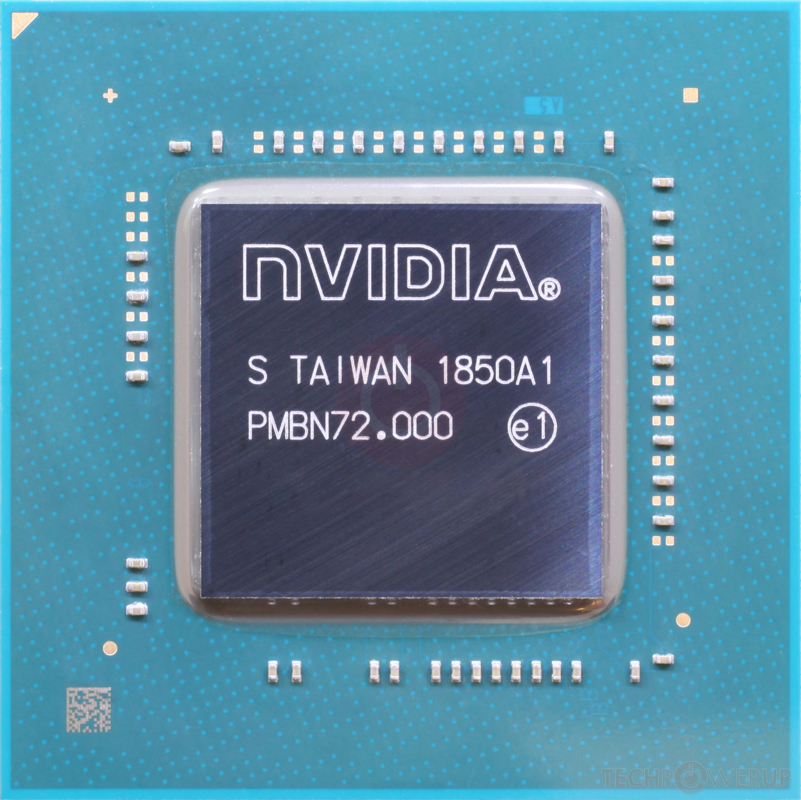
- TU117
- Cores
- 640
- TMUs
- 40
- ROPs
- 32
- Memory Size
- 4 GB
- Memory Type
- GDDR6
- Bus Width
- 128 bit

GPU
I/O
Top

Bottom
Recommended Gaming Resolutions:
- 1600x900
- 1920x1080
- 2560x1440
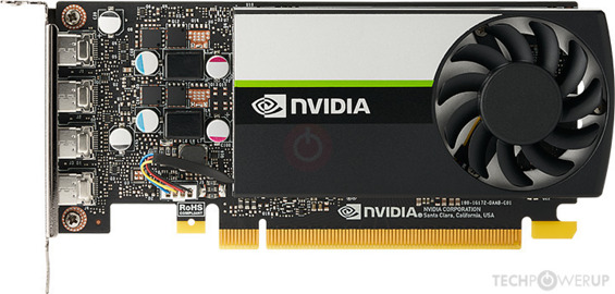
The T600 is a professional graphics card by NVIDIA, launched on April 12th, 2021. Built on the 12 nm process, and based on the TU117 graphics processor, the card supports DirectX 12. The TU117 graphics processor is an average sized chip with a die area of 200 mm² and 4,700 million transistors. Unlike the fully unlocked GeForce GTX 1650, which uses the same GPU but has all 896 shaders enabled, NVIDIA has disabled some shading units on the T600 to reach the product's target shader count. It features 640 shading units, 40 texture mapping units, and 32 ROPs. NVIDIA has paired 4 GB GDDR6 memory with the T600, which are connected using a 128-bit memory interface. The GPU is operating at a frequency of 735 MHz, which can be boosted up to 1335 MHz, memory is running at 1250 MHz (10 Gbps effective).
Being a single-slot card, the NVIDIA T600 does not require any additional power connector, its power draw is rated at 40 W maximum. Display outputs include: 4x mini-DisplayPort 1.4a. T600 is connected to the rest of the system using a PCI-Express 3.0 x16 interface.
Being a single-slot card, the NVIDIA T600 does not require any additional power connector, its power draw is rated at 40 W maximum. Display outputs include: 4x mini-DisplayPort 1.4a. T600 is connected to the rest of the system using a PCI-Express 3.0 x16 interface.
Graphics Processor
Graphics Card
- Release Date
- Apr 12th, 2021
- Generation
-
Quadro Turing
(Tx000)
- Predecessor
- Quadro Volta
- Successor
- Quadro Ampere
- Production
- Active
- Bus Interface
- PCIe 3.0 x16
Relative Performance
Based on TPU review data: "Performance Summary" at 1920x1080, 4K for 2080 Ti and faster.
Performance estimated based on architecture, shader count and clocks.
Clock Speeds
- Base Clock
- 735 MHz
- Boost Clock
- 1335 MHz
- Memory Clock
-
1250 MHz
10 Gbps effective
Memory
- Memory Size
- 4 GB
- Memory Type
- GDDR6
- Memory Bus
- 128 bit
- Bandwidth
- 160.0 GB/s
Render Config
- Shading Units
- 640
- TMUs
- 40
- ROPs
- 32
- SM Count
- 10
- L1 Cache
- 64 KB (per SM)
- L2 Cache
- 1024 KB
Theoretical Performance
- Pixel Rate
- 42.72 GPixel/s
- Texture Rate
- 53.40 GTexel/s
- FP16 (half)
- 3.418 TFLOPS (2:1)
- FP32 (float)
- 1.709 TFLOPS
- FP64 (double)
- 53.40 GFLOPS (1:32)
Board Design
- Slot Width
- Single-slot
- TDP
- 40 W
- Suggested PSU
- 200 W
- Outputs
- 4x mini-DisplayPort 1.4a
- Power Connectors
- None
- Board Number
- PG172 SKU 510
Graphics Features
- DirectX
- 12 (12_1)
- OpenGL
- 4.6
- OpenCL
- 3.0
- Vulkan
- 1.3
- CUDA
- 7.5
- Shader Model
- 6.7
TU117 GPU Notes
| NVENC: 5th Gen NVDEC: 4th Gen PureVideo HD: VP10 VDPAU: Feature Set J |
Apr 27th, 2024 03:15 EDT
change timezone
Latest GPU Drivers
New Forum Posts
- Should I install Windows 10 or 11 for my new device (1)
- The TPU UK Clubhouse (24789)
- List of NPU-optimized apps and games (0)
- rx 6500 xt anisotropic filtering not working (1)
- What phone you use as your daily driver? And, a discussion of them. (1497)
- Alphacool CORE 1 CPU block - bulging with danger of splitting? (35)
- What are you playing? (20541)
- Safe memory overclock for the rtx 4050? (8)
- Help me identify rx 580 card ? (1)
- Your PC ATM (34511)
Popular Reviews
- Ugreen NASync DXP4800 Plus Review
- HYTE THICC Q60 240 mm AIO Review
- MOONDROP x Crinacle DUSK In-Ear Monitors Review - The Last 5%
- Upcoming Hardware Launches 2023 (Updated Feb 2024)
- Thermalright Phantom Spirit 120 EVO Review
- Quick Look: MOONDROP CHU 2 Budget In-Ear Monitors
- FiiO K19 Desktop DAC/Headphone Amplifier Review
- AMD Ryzen 7 7800X3D Review - The Best Gaming CPU
- Alienware Pro Wireless Gaming Keyboard Review
- Corsair iCUE Link XC7 RGB Elite CPU Water Block Review
Controversial News Posts
- Windows 11 Now Officially Adware as Microsoft Embeds Ads in the Start Menu (136)
- Sony PlayStation 5 Pro Specifications Confirmed, Console Arrives Before Holidays (117)
- NVIDIA Points Intel Raptor Lake CPU Users to Get Help from Intel Amid System Instability Issues (106)
- AMD "Strix Halo" Zen 5 Mobile Processor Pictured: Chiplet-based, Uses 256-bit LPDDR5X (103)
- US Government Wants Nuclear Plants to Offload AI Data Center Expansion (98)
- AMD's RDNA 4 GPUs Could Stick with 18 Gbps GDDR6 Memory (95)
- Developers of Outpost Infinity Siege Recommend Underclocking i9-13900K and i9-14900K for Stability on Machines with RTX 4090 (85)
- Windows 10 Security Updates to Cost $61 After 2025, $427 by 2028 (84)