News Headlines
- Thu, Apr 25
- Fallout 4 next-gen upgrade goes live
- Mon, Apr 22
- Take-Two confirms more layoffs, cancelled projects by December 2024
- Wed, Apr 10
- Microsoft and NetEase to (re)launch core Blizzard games in China
- Fri, Mar 22
- Helldivers II already top-selling game of 2024 in US during launch month
- Tue, Mar 05
- Final Fantasy VII Rebirth tops UK charts during launch week
Related Articles
nForce 590: Foxconn C51XEM2AA Review - PAGE 4
Geordan Hankinson - Tuesday, May 23rd, 2006 Like ShareA spectacular board ought not be ruined by a mediocre BIOS implementation, and while we've been witness to such atrocities in the past, the C512XEM2AA is no victim to them. NVIDIA's reference BIOS design is as powerful and unique as is the board design.
Since we enthusiasts have seen more BIOSes than we have our own siblings, it's pointless to go over the standard panels present in nearly every BIOS implementation. It's a good thing, too, because it saves valuable time for some more detailed discussion of the NVIDIA implementation. Be prepared to get blown away by a BIOS design that actually makes sense and is easy to use.
Let's start with the Advanced Chipset Features menu, which is where all the loving begins:
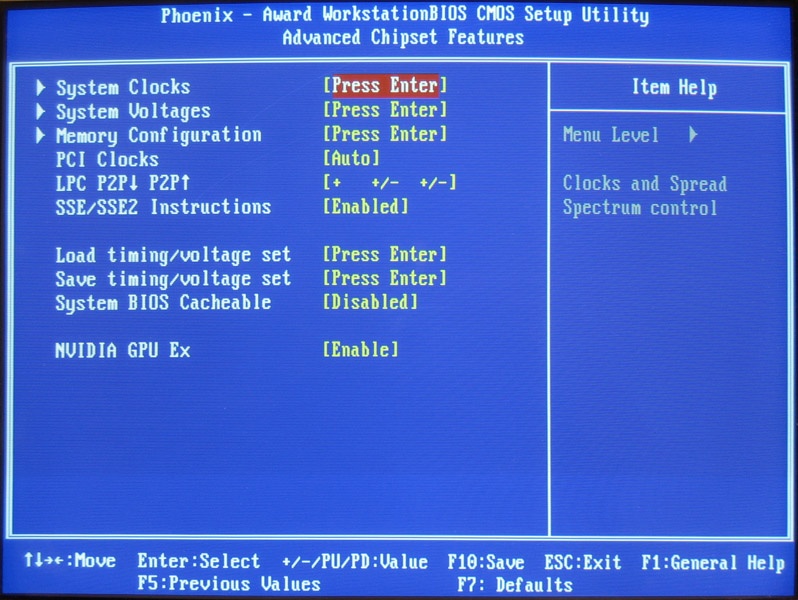
Right off the bat, clean organization shines through. Can we finally get rid of that painful trend of shoving the memory timings deep inside a "CPU options" menu? Or maybe digging through inane toggles just to be able to adjust a CPU multiplier? You bet.
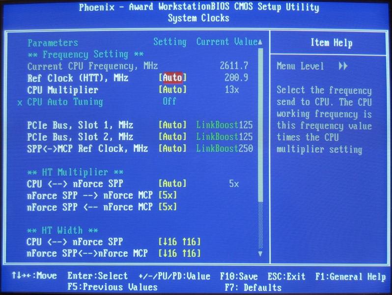
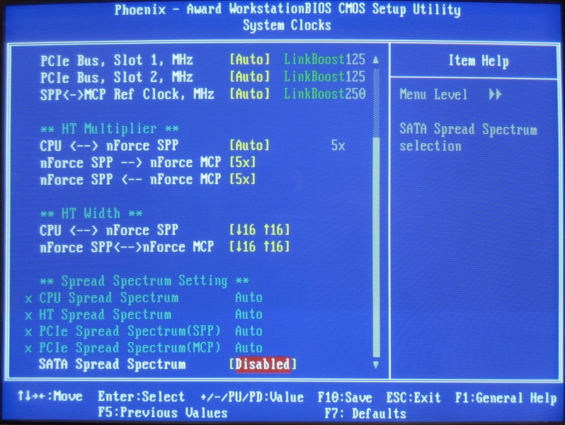
Here we can see the first of many design wins in this BIOS implementation. That second column of "current" values is something I've wanted to see done since being exposed to overclocking. I will not take the chance of crediting NVIDIA entirely for this, since I'm sure that it's been done before, but this is the first time that such a feature stands a chance of becoming mainstream.
Also of interest is the "LinkBoost" string, which is telling us that the PCI x16 slot clocks have been increased to 125 MHz (from 100 MHz), and that the north bridge/south bridge HyperTransport link speed has been increased to 250 MHz (from 200 MHz).
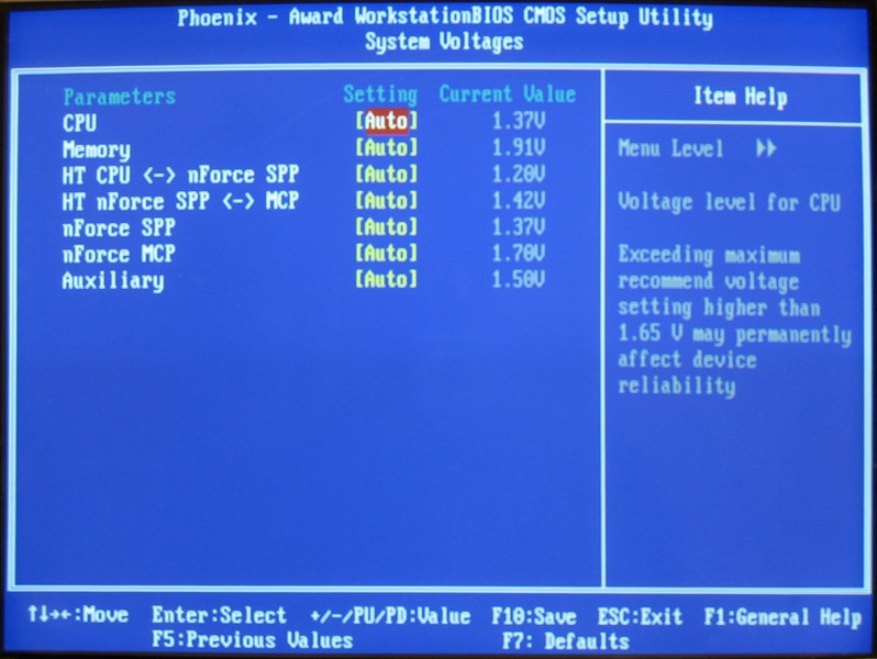
Next up is the System Voltages screen, which allows us some great flexibility in delivering extra juice to those components that depend on it. Once again, it is incredibly handy to have that extra column allowing you to take a peek at what the current setting is.
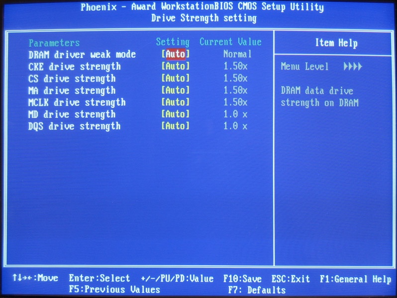
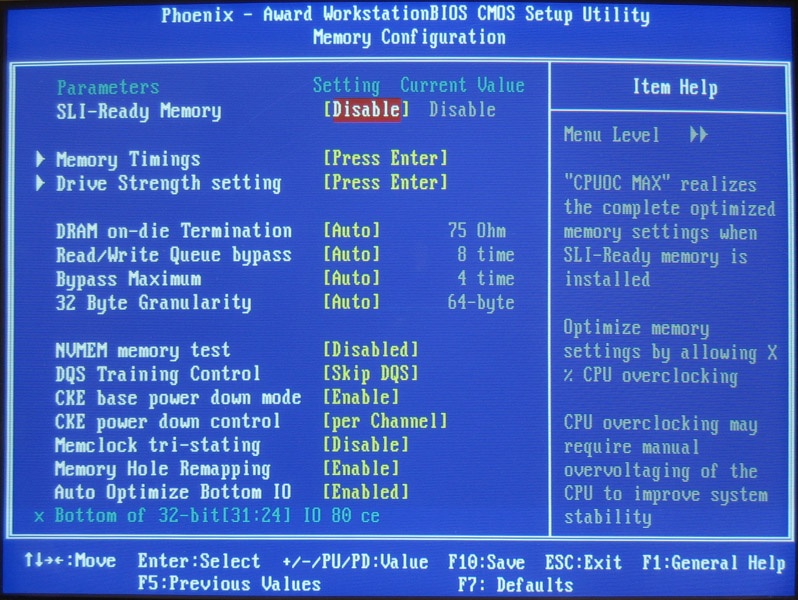
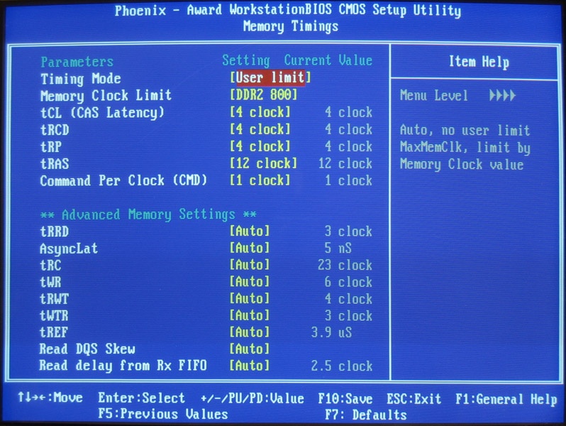
Continuing on with this theme of organization, we have the very nicely-laid out Memory Configuration screen. We'll let the photos speak for themselves, as there's absolutely too much to talk about here.
That is simply the best BIOS implementation I've seen to date. There is no hunting around for options, everything is sorted into logical hierarchies, and best of all ... the extra column illustrating the current setting does wonders for usability. The fact that many motherboard manufacturers will probably be following this reference design is liberating.
Article Index
|
|