Photonic Integrated Circuits for Passive Optical Networks: Outlook and Case Study of Integrated Quasi-Coherent Receiver

 ,
,
Abstract
:1. Introduction
2. Passive Optical Networks: Roadmap and Electro-Optical Implementations
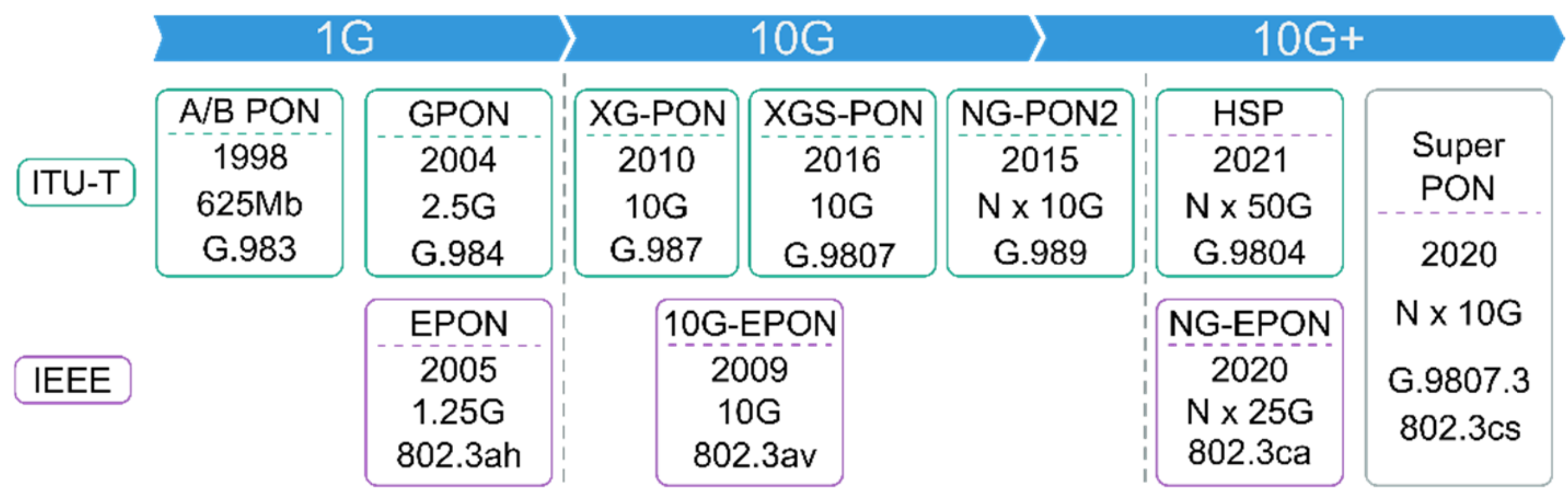
2.1. Passive Optical Networks Roadmap Review
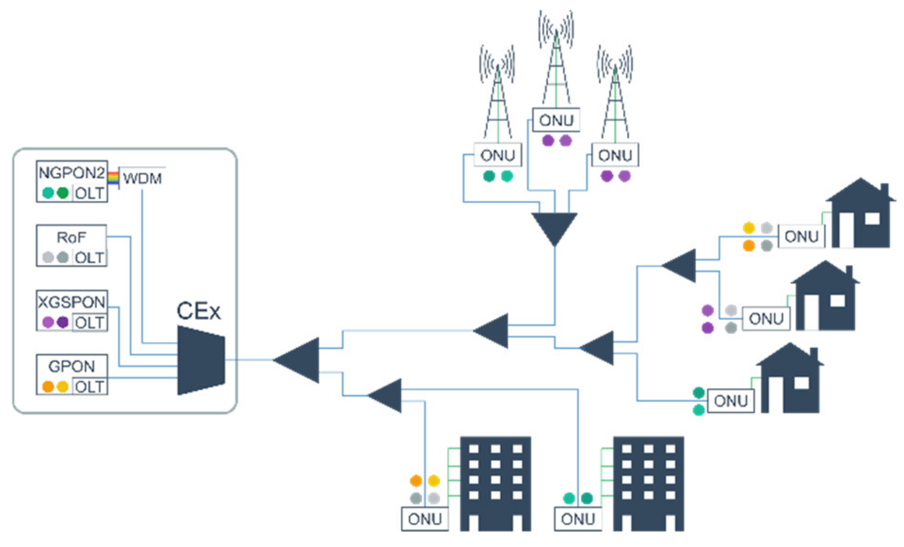
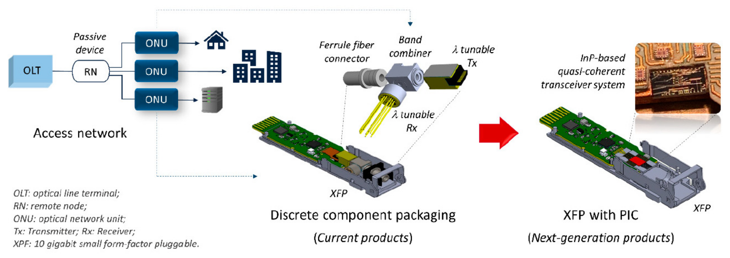
2.2. Passive Optical Networks and Their Electro-Optical Hardware
3. Photonic Integrated Circuits (PICs) Evolution and PON Applications
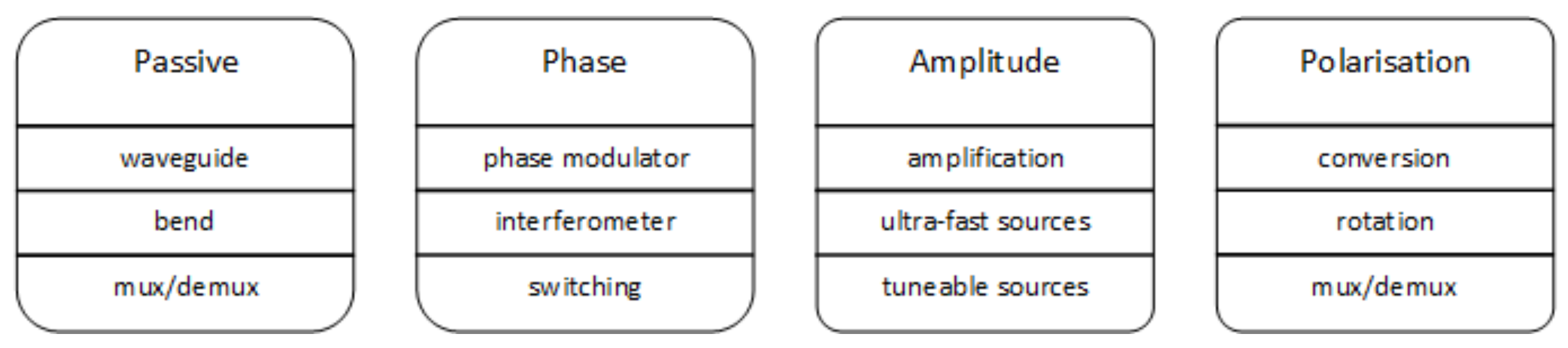
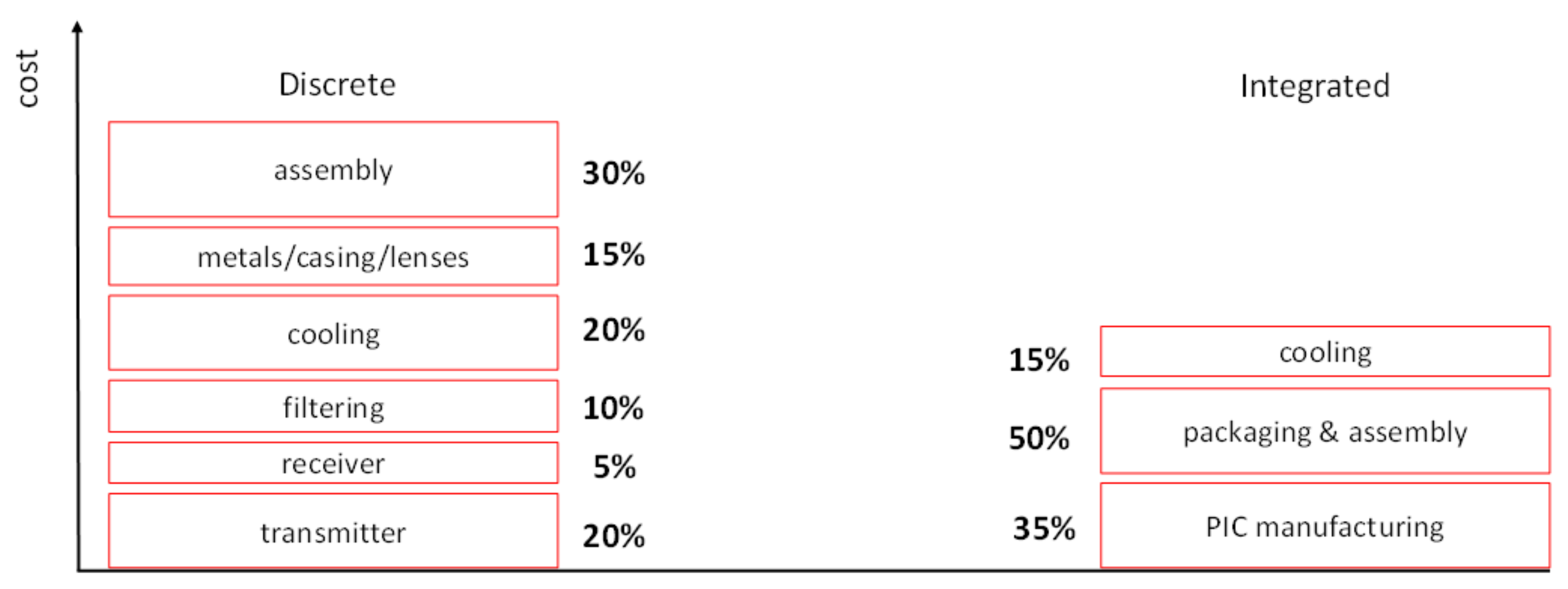
3.1. PIC from Concept to Generic Availability
3.2. An Outlook of PICs for PONs
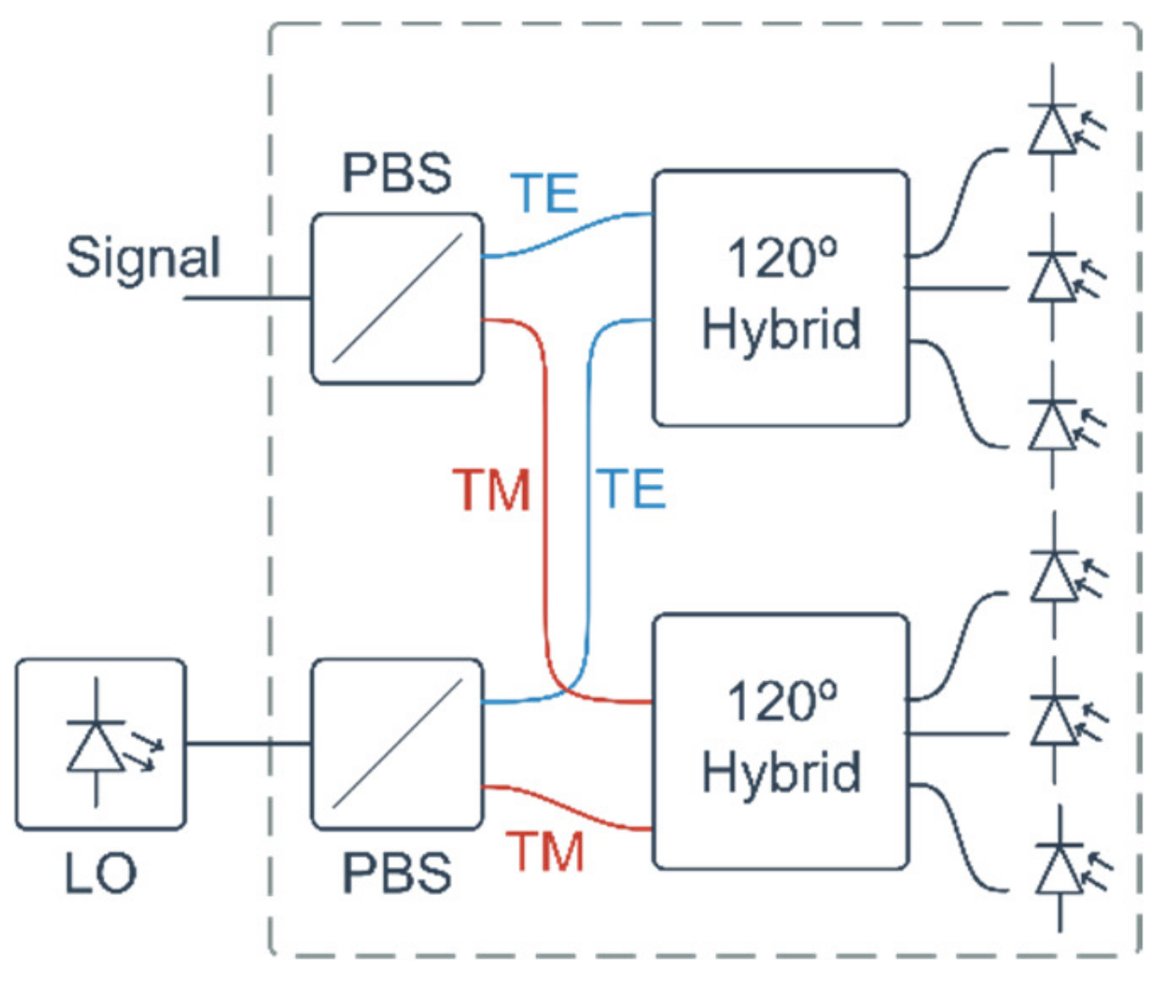
4. Quasi-Coherent Receiver Based on Co-Hosted InP PIC and SiGe ASIC
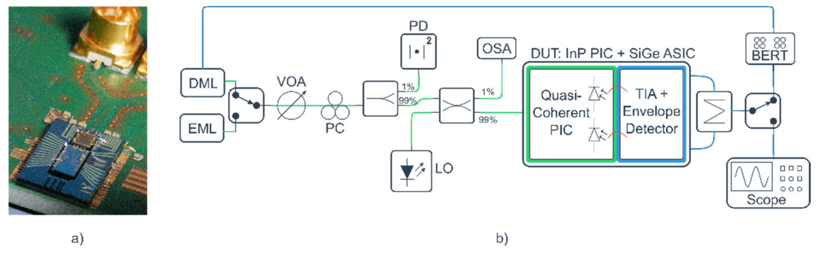
4.1. Co-Hosted Device and Experimental Setup
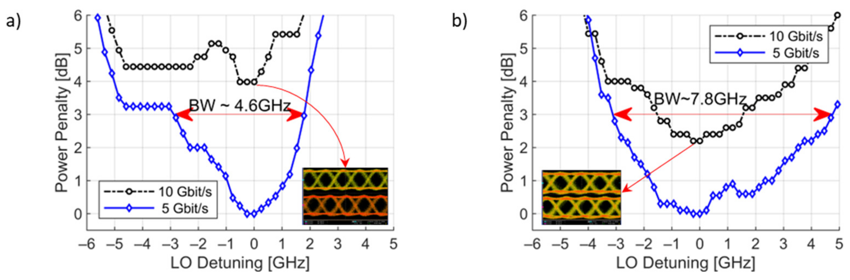
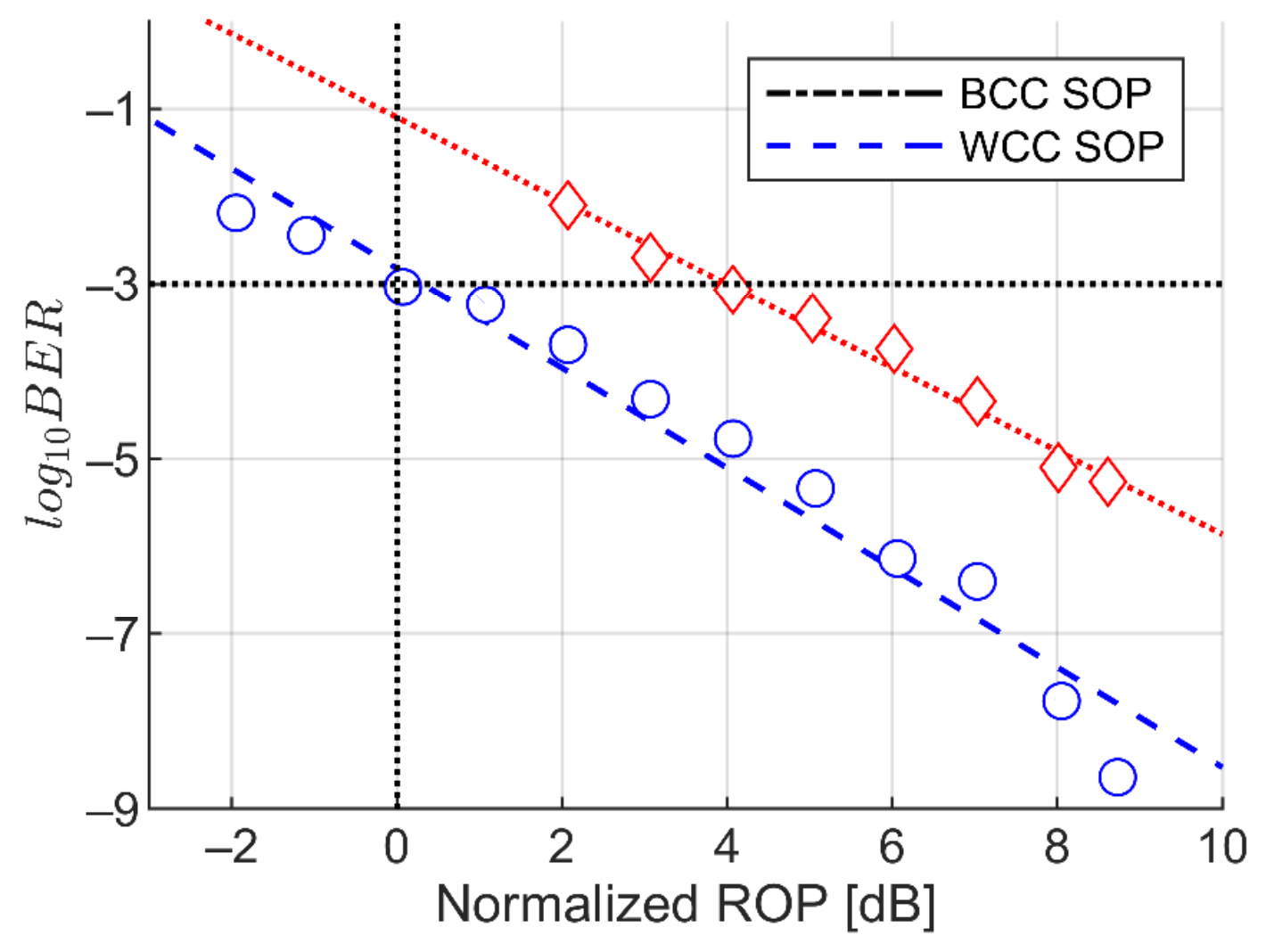
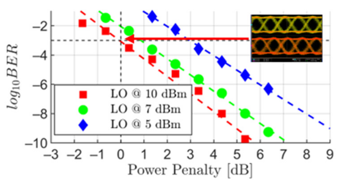
4.2. Experimental Results
5. Conclusions
Author Contributions
Funding
Institutional Review Board Statement
Informed Consent Statement
Data Availability Statement
Conflicts of Interest
References
- Wey, J.S. The Outlook for PON Standardization: A Tutorial. J. Light. Technol. 2020, 38, 31–42. [Google Scholar] [CrossRef]
- Gupta, H.; Gupta, P.; Kumar, P.; Gupta, A.K.; Kumar Mathur, P. Passive Optical Networks: Review and Road Ahead. In Proceedings of the TENCON 2018—IEEE Region 10 Annual International Conference, Jeju, Republic of Korea, 28–31 October 2018; Volume 2018-Octob, pp. 919–924. [Google Scholar] [CrossRef]
- Nesset, D. PON roadmap [invited]. J. Opt. Commun. Netw. 2017, 9, A71–A76. [Google Scholar] [CrossRef]
- ITU. ITU, ‘GPON Standard’. Available online: https://www.itu.int/rec/T-REC-G.984.1 (accessed on 21 November 2022).
- CISCO. Cisco Visual Networking Index (VNI): Forecast and Trends 2017–2022; White Paper; CISCO: Sydney, Australia, 2019. [Google Scholar]
- Dias, L.P.; Dos Santos, A.F.; Pereira, H.A.; de Andrade Almeida, R.C., Jr.; Giozza, W.F.; de Sousa, R.T., Jr.; Assis, K.D.R. Evolutionary Strategy for Practical Design of Passive Optical Networks. Photonics 2022, 9, 278. [Google Scholar] [CrossRef]
- ITU-T. Higher Speed Passive Optical Networks Requirements. Available online: https://www.itu.int/rec/T-REC-G.9804.1/en (accessed on 23 November 2022).
- ITU. Higher Speed Passive Optical Networks: Physical Media Dependent (PMD) Layer Specification. Available online: https://www.itu.int/rec/T-REC-G.9804.3-202109-I (accessed on 23 November 2022).
- Bonk, R.; Geng, D.; Khotimsky, D.; Liu, D.; Liu, X.; Luo, Y.; Nesset, D.; Oksman, V.; Strobel, R.; Van Hoof, W.; et al. 50G-PON: The First ITU-T Higher-Speed PON System. IEEE Commun. Mag. 2022, 60, 48–54. [Google Scholar] [CrossRef]
- Nesset, D. The Progress of Higher Speed Passive Optical Network Standardisation in ITU-T (Invited). In Proceedings of the 2021 European Conference on Optical Communication (ECOC), Bordeaux, France, 13–16 September 2021. [Google Scholar] [CrossRef]
- Rodrigues, C.; Rodrigues, F.; Pinho, C.; Bento, N.; Amorim, M.; Teixeira, A. 25 and 50G Optical Access Network Deployment Forecasts using Bi-Logistic curves. In Proceedings of the 2021 Optical Fiber Communications Conference and Exhibition (OFC), San Francisco, CA, USA, 6–10 June 2021. [Google Scholar]
- Agrawal, G.P. Fibre-Optic Communication Systems; John Wiley & Sons, Inc.: Hoboken, NJ, USA, 2002. [Google Scholar]
- PICadvanced S.A. Available online: https://www.picadvanced.store/product-page/sfp-gpon-olt-c (accessed on 23 November 2022).
- Broadband Forum. The Future of Passive Optical Networking Is Here NG-PON2, May 2019. Available online: https://www.broadband-forum.org/marketing/download/MU-437.pdf (accessed on 22 November 2022).
- Nesset, D. NG-PON2 technology and standards. J. Light. Technol. 2015, 33, 1136–1143. [Google Scholar] [CrossRef]
- Wey, J.S.; Nesset, D.; Valvo, M.; Grobe, K.; Roberts, H.; Luo, Y.; Smith, J. Physical layer aspects of NG-PON2 standards-Part 1: Optical link design [Invited]. J. Opt. Commun. Netw. 2016, 8, 33–42. [Google Scholar] [CrossRef]
- G989.2. 2014. Available online: https://www.itu.int/rec/T-REC-G.989.2 (accessed on 22 November 2022).
- Matsui, Y.; Li, W.; Roberts, H.; Bulthuis, H.; Deng, H.; Lin, L.; Roxlo, C. Transceiver for NG-PON2: Wavelength Tunablity for Burst Mode TWDM and Point-to-Point WDM. In Proceedings of the 2016 Optical Fiber Communications Conference and Exhibition (OFC), Anaheim, CA, USA, 20–24 March 2016. [Google Scholar]
- Van Veen, D.; Houtsma, V.; Porto, S.; Basavanhally, N.; Bolle, C.; Schmuck, H. Wavelength-stable burst-mode laser for next-generation PONs. J. Opt. Commun. Netw. 2019, 11, A155–A165. [Google Scholar] [CrossRef]
- Harstead, E.; Van Veen, D.; Houtsma, V.; Dom, P. Technology roadmap for time-division multiplexed passive optical networks (TDM PONs). J. Light. Technol. 2019, 37, 657–664. [Google Scholar] [CrossRef]
- Zhang, T. Tunable Laser Drivers for Next Generation WDM-Based PON Networks. In Proceedings of the 2019 Optical Fiber Communications Conference and Exhibition (OFC), San Diego, CA, USA, 3–7 March 2019. [Google Scholar]
- Gaudino, R.; Torres-Ferrera, P.; Wang, H.; Valvo, M.; Pagano, A.; Mercinelli, R.; Ferrero, V. Opportunities and Challenges When Using Low Bandwidth Optics for Higher Capacity PON Systems. In Proceedings of the 2020 Optical Fiber Communications Conference and Exhibition (OFC), San Diego, CA, USA, 8–12 March 2020. [Google Scholar]
- Coudyzer, G.; Ossieur, P.; Breyne, L.; La Porta, A.; Paredes, S.; Bauwelinck, J.; Yin, X. Study of burst-mode adaptive equalization for >25G PON applications [Invited]. J. Opt. Commun. Netw. 2020, 12, A104–A112. [Google Scholar] [CrossRef]
- Van Veen, D.; Houtsma, V. Transceiver Technologies for Next-Generation PON (Tutorial). In Proceedings of the 2020 Optical Fiber Communications Conference and Exhibition (OFC), San Diego, CA, USA, 8–12 March 2020. [Google Scholar]
- Torres-Ferrera, P.; Milite, V.; Ferrero, V.; Valvo, M.; Mercinelli, R.; Gaudino, R. Burst-mode equalization strategies in 25 Gbps US-PON using duobinary and 10G-class APD for 20-km in C-band. In Proceedings of the 2019 Optical Fiber Communications Conference and Exhibition (OFC), San Diego, CA, USA, 3–7 March 2019. [Google Scholar]
- Udalcovs, A.; Salgals, T.; Zhang, L.; Pang, X.; Djupsjöbacka, A.; Spolitis, S.; Bobrovs, V.; Popov, S.; Ozolins, O. Optical power budget of 25+ Gbps IM/DD PON with digital signal post-equalization. Appl. Sci. 2020, 10, 6106. [Google Scholar] [CrossRef]
- Wang, H.; Torres-Ferrera, P.; Ferrero, V.; Gaudino, R. Experimental study on 25 gbps c-band pon over up to 25 km smf using a 10g-class dml + apd im-dd system. Photonics 2021, 8, 328. [Google Scholar] [CrossRef]
- Hong, C.; Shi, B.; Qi, F.; Cai, P.; Duan, Y.; Hou, G.; Su, T.; Chiu, T.; Li, S.; Chen, W.; et al. High Speed Ge/Si Avalanche Photodiode with High Sensitivity for 50Gbit/s and 100Gbit/s Optical Access Systems. In Proceedings of the 2022 Optical Fiber Communications Conference and Exhibition (OFC), San Diego, CA, USA, 6–10 March 2022. [Google Scholar]
- Dai, X.; Debregeas, H.; Da Rold, G.; Carrara, D.; Louarn, K.; Valdeiglesias, E.D.; Lelarge, F. Versatile Externally Modulated Lasers Technology for Multiple Telecommunication Applications. IEEE J. Sel. Top. Quantum Electron. 2021, 27, 3400412. [Google Scholar] [CrossRef]
- Watanabe, T.; Sakaida, N.; Yasaka, H.; Kano, F.; Koga, M. Transmission performance of chirp-controlled signal by using semiconductor optical amplifier. J. Light. Technol. 2000, 18, 1069–1077. [Google Scholar] [CrossRef]
- Rosales, R.; Cano, I.; Nesset, D.; Zhicheng, Y.; Brenot, R.; Dubrovina, N.; Duran-Valdeiglesias, E.; Debregeas, H.; Carrara, D.; Lelarge, F. First Demonstration of an E2 Class Downstream Link for 50Gb/s PON at 1342nm. In Proceedings of the 2020 European Conference on Optical Communications (ECOC), Brussels, Belgium, 6–10 December 2020. [Google Scholar] [CrossRef]
- Zhang, D.; Liu, D.; Nesset, D.; Wu, X.; Ming, J. Carrier Lab Trial of a Real Time 50G-PON Prototype. In Proceedings of the 2021 European Conference on Optical Communication (ECOC), Bordeaux, France, 13–16 September 2021. [Google Scholar] [CrossRef]
- Rosales, R.; Cano, I.; Nesset, D.; Brenot, R.; Dubrovina, N.; Durán-Valdeiglesias, E.; Debregeas, H. Achieving high budget classes in the downstream link of 50G-PON. J. Opt. Commun. Netw. 2021, 13, D13–D21. [Google Scholar] [CrossRef]
- Rosales, R.; Cano, I.N.; Nesset, D.; Brenot, R.; Talli, G. 50G-PON Downstream Link up to 40 km with a 1342 nm Integrated EML+SOA. IEEE Photonics Technol. Lett. 2022, 34, 306–308. [Google Scholar] [CrossRef]
- Simon, G.; Saliou, F.; Potet, J.; Chanclou, P.; Rosales, R.; Cano, I.N.; Nesset, D. 50Gb/s Real-Time Transmissions with Upstream Burst-Mode for 50G-PON using a Common SOA Pre-amplifier/Booster at the OLT. In Proceedings of the 2020 Optical Fiber Communications Conference and Exhibition (OFC), San Diego, CA, USA, 6–10 March 2022. [Google Scholar]
- Li, Z.; Yin, F.; Huang, X.; Ma, Z.; Song, Y.; Yi, L. Demonstration of a 50G-PON with a 45-dB power budget using an IQ-interleaved coherent detection scheme. Opt. Express 2021, 29, 32523–32534. [Google Scholar] [CrossRef]
- Zhu, Y.; Yang, B.; Zhong, Y.; Liu, Z.; Guo, Y.; Wey, J.S.; Huang, X.; Ma, Z. Performance Comparison of Coherent and Direct Detection Schemes for 50G PON. In Proceedings of the 2020 Optical Fiber Communications Conference and Exhibition (OFC), San Diego, CA, USA, 8–12 March 2020. [Google Scholar]
- Shahpari, A.; Ferreira, R.; Ribeiro, V.; Sousa, A.; Ziaie, S.; Tavares, A.; Vujicic, Z.; Guiomar, F.P.; Reis, J.D.; Pinto, A.N.; et al. Coherent ultra dense wavelength division multiplexing passive optical networks. Opt. Fiber Technol. 2015, 26, 100–107. [Google Scholar] [CrossRef]
- Shahpari, A.; Ferreira, R.M.; Luis, R.S.; Vujicic, Z.; Guiomar, F.P.; Reis, J.D.; Teixeira, A.L. Coherent Access: A Review. J. Light. Technol. 2017, 35, 1050–1058. [Google Scholar] [CrossRef]
- COCOUNUT Project. Available online: http://www.ict-coconut.eu (accessed on 23 November 2022).
- Prat, J. Technologies for a cost effective UDWDM-PON. In Proceedings of the 2015 Optical Fiber Communications Conference and Exhibition (OFC), Los Angeles, CA, USA, 22–26 March 2015. [Google Scholar]
- Ciaramella, E. Polarization-independent receivers for low-cost coherent OOK systems. IEEE Photonics Technol. Lett. 2014, 26, 548–551. [Google Scholar] [CrossRef]
- Ciaramella, E. Assessment of a Polarization-Independent DSP-Free Coherent Receiver for Intensity-Modulated Signals. J. Light. Technol. 2020, 38, 676–683. [Google Scholar] [CrossRef]
- Tabares, J.A.; Ghasemi, S.; Velásquez, J.C.; Prat, J. Coherent Ultra-Dense WDM-PON Enabled by Complexity-Reduced Digital Transceivers. J. Light. Technol. 2020, 38, 1305–1313. [Google Scholar] [CrossRef]
- Lavery, D.; Gerard, T.; Erkılınç, S.; Liu, Z.; Galdino, L.; Bayvel, P.; Killey, R.I. Opportunities for optical access network transceivers beyond OOK [invited]. J. Opt. Commun. Netw. 2019, 11, A186–A195. [Google Scholar] [CrossRef]
- Lavery, D.; Bayvel, P.; Killey, R. Coherent Technologies for Passive Optical Networks. In Proceedings of the 2019 IEEE Photonics Society Summer Topical Meeting Series (SUM), Ft. Lauderdale, FL, USA, 8–10 July 2019. [Google Scholar] [CrossRef]
- Altabas, J.A.; Valdecasa, G.S.; Didriksen, M.; Lazaro, J.A.; Garces, I.; Monroy, I.T.; Jensen, J.B. Real-time 10Gbps polarization independent quasicoherent receiver for NG-PON2 access networks. J. Light. Technol. 2019, 37, 651–656. [Google Scholar] [CrossRef]
- Miller, S.E. Integrated Optics: An Introduction. Bell Syst. Tech. J. 1969, 48, 2059–2069. [Google Scholar] [CrossRef]
- Nagarajan, R.; Joyner, C.H.; Schneider, R.P.; Bostak, J.S.; Butrie, T.; Dentai, A.G.; Dominic, V.G.; Evans, P.W.; Kato, M.; Kauffman, M.; et al. Large-scale photonic integrated circuits. IEEE J. Sel. Top. Quantum Electron. 2005, 11, 50–62. [Google Scholar] [CrossRef]
- Gao, Y.; Lo, J.-C.; Lee, S.; Patel, R.; Zhu, L.; Nee, J.; Tsou, D.; Carney, R.; Sun, J. High-Power, Narrow-Linewidth, Miniaturized Silicon Photonic Tunable Laser with Accurate Frequency Control. J. Light. Technol. 2020, 38, 265–271. [Google Scholar] [CrossRef]
- CISCO. Available online: https://www.cisco.com/c/en/us/products/collateral/interfaces-modules/transceiver-modules/datasheet-c78-743172.html (accessed on 23 November 2022).
- INTEL No Title. Available online: https://www.intel.com/content/www/us/en/architecture-and-technology/silicon-photonics/silicon-photonics-overview.html (accessed on 23 November 2022).
- Smit, M.; Leijtens, X.; Bente, E.; van der Tol, J.; Ambrosius, H.; Robbins, D.; Wale, M.; Grote, N.; Schell, M. A generic foundry model for InP-based photonic ICs. In Proceedings of the 2012 Optical Fiber Communications Conference and Exhibition (OFC), Los Angeles, CA, USA, 4–8 March 2012. [Google Scholar]
- Smit, M.; Leijtens, X.; Ambrosius, H.; Bente, E.; van der Tol, J.; Smalbrugge, B.; de Vries, T.; Geluk, E.J.; Bolk, J.; van Veldhoven, R.; et al. An introduction to InP-based generic integration technology. Semicond. Sci. Technol. 2014, 29, 083001. [Google Scholar] [CrossRef]
- JEPPIX Platform. Available online: https://www.jeppix.eu/ (accessed on 24 November 2022).
- ePIXfab Platform. Available online: https://epixfab.eu/ (accessed on 24 November 2022).
- Lionix International BVBV. Available online: https://www.lionix-international.com/ (accessed on 24 November 2022).
- AIM Photonics. Available online: http://www.aimphotonics.com/ (accessed on 24 November 2022).
- Jeppix. JePPIX Roadmap 2018: The Road to a Multi-Billion Euro Market in Integrated Photonics. Available online: http://wipe.jeppix.eu/public/images/JePPIX-Roadmap-may2018_FINAL.pdf (accessed on 24 November 2022).
- Smit, M.; van der Tol, J.; Hill, M. Moore’s law in photonics. Laser Photonics Rev. 2012, 6, 1–13. [Google Scholar] [CrossRef]
- Smit, M.; Williams, K.; Van Der Tol, J. Past, present, and future of InP-based photonic integration. APL Photonics 2019, 4, 050901. [Google Scholar] [CrossRef]
- Van Der Tol, J.J.G.M.; Jiao, Y.; Van Engelen, J.P.; Pogoretskiy, V.; Kashi, A.A.; Williams, K. InP Membrane on Silicon (IMOS) Photonics. IEEE J. Quantum Electron. 2020, 56, 6300107. [Google Scholar] [CrossRef]
- Fedeli, J.-M.; Nicoletti, S.; Lagae, L.; Artundo, I.; O’Brien, P. EU pilot lines for integrated photonics. In Proceedings of the 2017 IEEE 14th International Conference on Group IV Photonics (GFP), Berlin, Germany, 23–25 August 2017; pp. 79–80. [Google Scholar] [CrossRef]
- Jans, H.; O’Brien, P.; Artundo, I.; Porcel, M.; Hoofman, R.; Geuzebroek, D.; Dumon, P.; Vliet, M.; Witzens, J.; Bourguignon, E.; et al. Integrated bio-photonics to revolutionize health care enabled through PIX4life and PIXAPP. In Proceedings of the Progress in Biomedical Optics and Imaging—Proceedings of SPIE, San Francisco, CA, USA, 27 January–1 February 2018; Volume 10506. [Google Scholar] [CrossRef]
- Latkowski, S.; Pustakhod, D.; Yao, W.; Leijtens, X.; Williams, K. Test Methods and Processes in Manufacturing Chain of Photonic Integrated Circuits. In Proceedings of the International Conference on Transparent Optical Networks, Bucharest, Romenia, 1–5 July 2018. [Google Scholar] [CrossRef]
- O’Brien, P. Scaling of Integrated Photonic Packaging for Volume Manufacture. In Proceedings of the International Conference on Optical MEMS and Nanophotonics (OMN), Lausanne, Switzerland, 29 July–2 August 2018. [Google Scholar] [CrossRef]
- Carroll, L.; Lee, J.-S.; Scarcella, C.; Gradkowski, K.; Duperron, M.; Lu, H.; Zhao, Y.; Eason, C.; Morrissey, P.; Rensing, M.; et al. Photonic packaging: Transforming silicon photonic integrated circuits into photonic devices. Appl. Sci. 2016, 6, 426. [Google Scholar] [CrossRef] [Green Version]
- Gradkowski, K.; Eason, C.; Lee, J.S.; Bernabe, S.; Temporiti, E.; Carroll, L.; O’Brien, P. Thermal challenges for packaging integrated photonic devices. In Proceedings of the 2016 6th Electronic System-Integration Technology Conference (ESTC), Grenoble, France, 13–15 September 2016. [Google Scholar] [CrossRef]
- Punch, J. Thermal challenges in photonic integrated circuits. In Proceedings of the 2012 13th International Conference on Thermal, Mechanical and Multi-Physics Simulation and Experiments in Microelectronics and Microsystems, Cascais, Portugal, 16–18 April 2012. [Google Scholar] [CrossRef]
- Punch, J. Microfluidics for the thermal control of Photonics Integrated Circuits. In Proceedings of the 2018 19th International Conference on Thermal, Mechanical and Multi-Physics Simulation and Experiments in Microelectronics and Microsystems, Tolouse, France, 15–18 April 2018; pp. 1–5. [Google Scholar] [CrossRef]
- Kyatam, S.; Mukherjee, D.; Neto, H.; Mendes, J.C. Thermal management of photonic integrated circuits: Impact of holder material and epoxies. Appl. Opt. 2019, 58, 6126–6135. [Google Scholar] [CrossRef]
- Huiszoon, B.; Lawniczuk, K.; de Laat, M.M.; Duijn, R.L.; Broeke, R.G.; Leijtens, X.J.M.; van den Hoven, G.N. Application specific photonic integrated circuits for FlexPON: Progress of the EuroPIC project. In Proceedings of the 14th International Converence on Transparent Optical Networks (ICTON), Coventry, UK, 2–5 July 2012. [Google Scholar] [CrossRef]
- Zhao, J.; Chen, X.; Zhou, N.; Huang, X.; Cao, M.; Wang, L.; Liu, W. Experimental demonstration of monolithically integrated 16 channel DFB laser array fabricated by nanoimprint lithography with AWG multiplexer and SOA for WDM-PON application. Opt. Commun. 2015, 339, 78–85. [Google Scholar] [CrossRef]
- Kleinert, M.; Zhang, Z.; de Felipe, D.; Zawadzki, C.; Novo, A.M.; Brinker, W.; Möhrle, M.; Keil, N. Recent progress in InP/polymer-based devices for telecom and data center applications. In Proceedings of the SPIE Integrated Optics: Devices, Materials, and Technologies XIX, San Francisco, CA, USA, 27 February 2015; Volume 9365. [Google Scholar] [CrossRef]
- Zhang, Q.; Fu, S.; Man, J.; Li, Z.; Cherchi, M.; Heimala, P.; Harjanne, M.; Fei, S.; Hiltunen, M.; Aalto, T.; et al. Low-loss and polarization-insensitive photonic integrated circuit based on micron-scale SOI platform for High Density TDM PONs. In Proceedings of the 2017 Optical Fiber Communications Conference and Exhibition (OFC), Los Angeles, CA, USA, 19–23 March 2017. [Google Scholar]
- Pachnicke, S.; Zhu, J.; Lawin, M.; Wonfor, A.; Eiselt, M.; Cush, R.; Turner, R.; Firth, P.; Wale, M.; Penty, R.V.; et al. Novel WDM-PON system with shared wavelength locking and full C-band tunability. In Proceedings of the Photonics Networks; 15. ITG Symposium, Leipzig, Germany, 5–6 May 2014; pp. 58–62. [Google Scholar]
- Nadimi Goki, P.; Imran, M.; Porzi, C.; Toccafondo, V.; Fresi, F.; Cavaliere, F.; Potì, L. Lossless WDM PON photonic integrated receivers including SOAs. Appl. Sci. 2019, 9, 2457. [Google Scholar] [CrossRef]
- Zali, A.R.; Kleijn, S.; Augustin, L.; Tessema, N.M.; Prifti, K.; Stabile, R.; Calabretta, N. Design and Fabrication of Low Polarization Dependent Bulk SOA Co-Integrated with Passive Waveguides for Optical Network Systems. J. Light. Technol. 2022, 40, 1083–1091. [Google Scholar] [CrossRef]
- Paśnikowska, A.; Stopiński, S.; Piramidowicz, R. Integrated InP-based multichannel transmitters for WDM-PON system. In Proceedings of the 2019 Conference on Lasers and Electro-Optics Europe & European Quantum Electronics Conference (CLEO/Europe-EQEC), Munich, Germany, 23–27 June 2019. [Google Scholar] [CrossRef]
- Tavares, A.; Lopes, A.; Rodrigues, C.; Mãocheia, P.; Mendes, T.; Brandão, S.; Rodrigues, F.; Ferreira, R.; Teixeira, A. Photonic integrated transmitter and receiver for NG-PON2. In Proceedings of the SPIE—The International Society for Optical Engineering, Aveiro, Portugal, 22 August 2014; Volume 9286. [Google Scholar] [CrossRef]
- Sasaki, H. Development of silicon photonics integrated circuits for next generation optical access networks. In Proceedings of the 2019 2nd International Symposium on Devices, Circuits and Systems (ISDCS), Higashi-Hiroshima, Japan, 6–8 March 2019. [Google Scholar] [CrossRef]
- O’Carroll, J. Photonic integrated circuits for NGPON2 Tunable ONUs. In Proceedings of the 2019 Optical Fiber Communications Conference and Exhibition (OFC), San Diego, CA, USA, 11–15 March 2018. [Google Scholar]
- Teixeira, A. Photonic Integrated Circuits for NG-PON2 ONU Transceivers. In Proceedings of the 2019 Optical Fiber Communications Conference and Exhibition (OFC), San Diego, CA, USA, 3–7 March 2019. [Google Scholar]
- Pinho, C.; Rodrigues, F.; Tavares, A.M.; Rodrigues, C.; Rodrigues, C.E.; Teixeira, A. Photonic integrated circuits for NGPON2 ONU transceivers (Invited). Appl. Sci. 2020, 10, 4024. [Google Scholar] [CrossRef]
- Seimetz, M.; Weinert, C.-M. Options, feasibility, and availability of 2 × 4 90° hybrids for coherent optical systems. J. Light. Technol. 2006, 24, 1317–1322. [Google Scholar] [CrossRef]
- Dong, P.; Xie, C.; Buhl, L.L. Monolithic coherent receiver based on 120-degree optical hybrids on silicon. In Proceedings of the 2019 Optical Fiber Communications Conference and Exhibition (OFC), San Francisco, CA, USA, 9–13 March 2014. [Google Scholar]
- Hoefler, G.E.; Zhou, Y.; Anagnosti, M.; Bhardwaj, A.; Abolghasem, P.; James, A.; Luna, S.; Debackere, P.; Dentai, A.; Vallaitis, T.; et al. Foundry Development of System-On-Chip InP-Based Photonic Integrated Circuits. IEEE J. Sel. Top. Quantum Electron. 2019, 25, 6100317. [Google Scholar] [CrossRef]
- Hosseini, A.; Lu, M.; Going, R.; Samra, P.; Amiralizadeh, S.; Nguyen, A.; Rahn, J.; Dominic, V.; Awadalla, A.; Corzine, S.; et al. Extended C-band tunable multi-channel InP-based coherent receiver PICs. Opt. Express 2017, 25, 18853–18862. [Google Scholar] [CrossRef]
- Lauermann, M.; Going, R.; Maher, R.; Lu, M.; Ko, W.; Studenkov, P.; Ferrara, J.; Hosseini, A.; Corzine, S.; Rahn, J.; et al. Multi-channel, widely-tunable coherent transmitter and receiver PICs Operating at 88Gbaud/16-QAM. In Proceedings of the 2017 Optical Fiber Communications Conference and Exhibition (OFC), Los Angeles, CA, USA, 19–23 March 2017. [Google Scholar]
- Going, R.; Wolf, S.; Maher, R.; Studenkov, P.; Lal, V.; Tsai, H.-S.; Corzine, S.; Zhang, J.; Behnia, B.; Giovanni, C.D.; et al. InP-based coherent pics for 100 gbaud operation. In OSA Advanced Photonics Congress (AP) 2019 (IPR, Networks, NOMA, SPPCom, PVLED); Optica Publishing Group: Washington, DC, USA, 2019; OSA Technical Digest; paper SpM4E.3. [Google Scholar] [CrossRef]
- Lal, V.; Studenkov, P.; Frost, T.; Tsai, H.; Behnia, B.; Osenbach, J.; Wolf, S.; Going, R.; Porto, S.; Maher, R.; et al. 1.6Tbps Coherent 2-Channel Transceiver using a Monolithic Tx/Rx InP PIC and Single SiGe ASIC. In Proceedings of the 2020 Optical Fiber Communications Conference and Exhibition (OFC), San Diego, CA, USA, 8–12 March 2020. [Google Scholar]
- Saber, M.G.; Osman, M.; Patel, D.; Samani, A.; El-Fiky, E.; Alam, M.S.; Shahriar, K.A.; Xing, Z.; Jacques, M.; Dortschy, B.; et al. Demonstration of a 120° hybrid based simplified coherent receiver on SOI for high speed PON applications. Opt. Express 2018, 26, 31222–31232. [Google Scholar] [CrossRef]
- Takechi, M.; Tateiwa, Y.; Kurokawa, M.; Yagi, H.; Hara, H. Compact optical receivers for coherent optical communication. SEI Tech. Rev. October 2017, 24–28. [Google Scholar]
- Runge, P.; Zhou, G.; Ganzer, F.; Seifert, S.; Mutschall, S.; Seeger, A. Polarisation insensitive coherent receiver PIC for 100Gbaud communication. In Proceedings of the 2016 Optical Fiber Communications Conference and Exhibition (OFC), Anaheim, CA, USA, 20–24 March 2016. [Google Scholar]
- Runge, P.; Zhou, G.; Beckerwerth, T.; Ganzer, F.; Keyvaninia, S.; Seifert, S.; Ebert, W.; Mutschall, S.; Seeger, A.; Schell, M. Waveguide Integrated Balanced Photodetectors for Coherent Receivers. IEEE J. Sel. Top. Quantum Electron. 2018, 24, 6100307. [Google Scholar] [CrossRef]
- Altabas, A.; Izquierdo, D.; Clemente, J.; Sarmiento, S.; Valdecasa, G.; Squartecchia, M.; Suhr, L.; Gallardo, O.; Lopez, A.; Losada, M.; et al. Advanced technologies for coherent access networks. In Proceedings of the International Conference on Transparent Optical Networks, Angers, France, 9–13 July 2019. [Google Scholar] [CrossRef]
- Valdecasa, G.S.; Puertas, O.G.; Altabas, J.A.; Squartecchia, M.; Jensen, J.B.; Johansen, T.K. High-Speed SiGe BiCMOS Detector Enabling a 28 Gbps Quasi-Coherent Optical Receiver. IEEE Trans. Circuits Syst. II Express Briefs 2022, 69, 964–968. [Google Scholar] [CrossRef]
- Valdecasa, G.S.; Altabas, J.A.; Kupska, M.; Jensen, J.B.; Johansen, T.K. A 5–50 GHz sige BiCMOS linear transimpedance amplifier with 68 dbΩ differential gain towards highly integrated quasi-coherent receivers. Electronics 2021, 10, 2349. [Google Scholar] [CrossRef]
- Johansen, T.K.; Valdecasa, G.; Kupska, M.; Altabas, J.; Gallardo, O.; Squartecchia, M.; Jensen, J. A 7-30 GHz, 80-dB Ω Noise-Optimized, Bandpass-Like TIA in 130 nm SiGe BiCMOS Technology for Quasi-Coherent Optical Receivers. In Proceedings of the 2021 16th European Microwave Integrated Circuits Conference (EuMIC), London, UK, 3–4 April 2022; pp. 173–176. [Google Scholar]
- Rodrigues, F.; Santos, J.; Rodrigues, C.; Teixeira, A. Hybrid PIC+ASIC quasi-coherent receiver for TWDM-PON. In Proceedings of the 2022 13th International Symposium on Communication Systems, Networks and Digital Signal Processing, CSNDSP 2022, Porto, Portugal, 20–22 July 2022; pp. 646–648. [Google Scholar] [CrossRef]
- Soares, F.M.; Baier, M.; Gaertner, T.; Grote, N.; Moehrle, M.; Beckerwerth, T.; Runge, P.; Schell, M. InP-Based Foundry PICs for Optical Interconnects. Appl. Sci. 2019, 9, 1588. [Google Scholar] [CrossRef]
- Glance, B. Polarization independent coherent optical receiver. J. Light. Technol. 1987, 5, 274–276. [Google Scholar] [CrossRef]


| Standard | Upstream | Downstream | |||||||||
|---|---|---|---|---|---|---|---|---|---|---|---|
| Wavelength (nm) | Max. Bit Rate (Gbps) | Max. Output Power (dBm) | Sensitivity (dBm) | Commercial Availability | Wavelength (nm) | Max. Bit Rate ( Gbps) | Max. Output Power (dBm) | Sensitivity (dBm) | Commercial Availability | ||
| GPON | Regular | 1290–1330 | 1.244 | 4 C+ | −28 BER 1E-10 | Mass | 1480–1500 | 2.488 | 7 C+ | −32 BER 1E-10 | Mass |
| Narrow | 1300–1320 | ||||||||||
| XGSPON | 1260–1280 | 9.953 | 9 N2 | −28 BER 10E-3 | Mass | 1575–1580 | 9.953 | 9 N2 | −28 BER 10E-3 | Mass | |
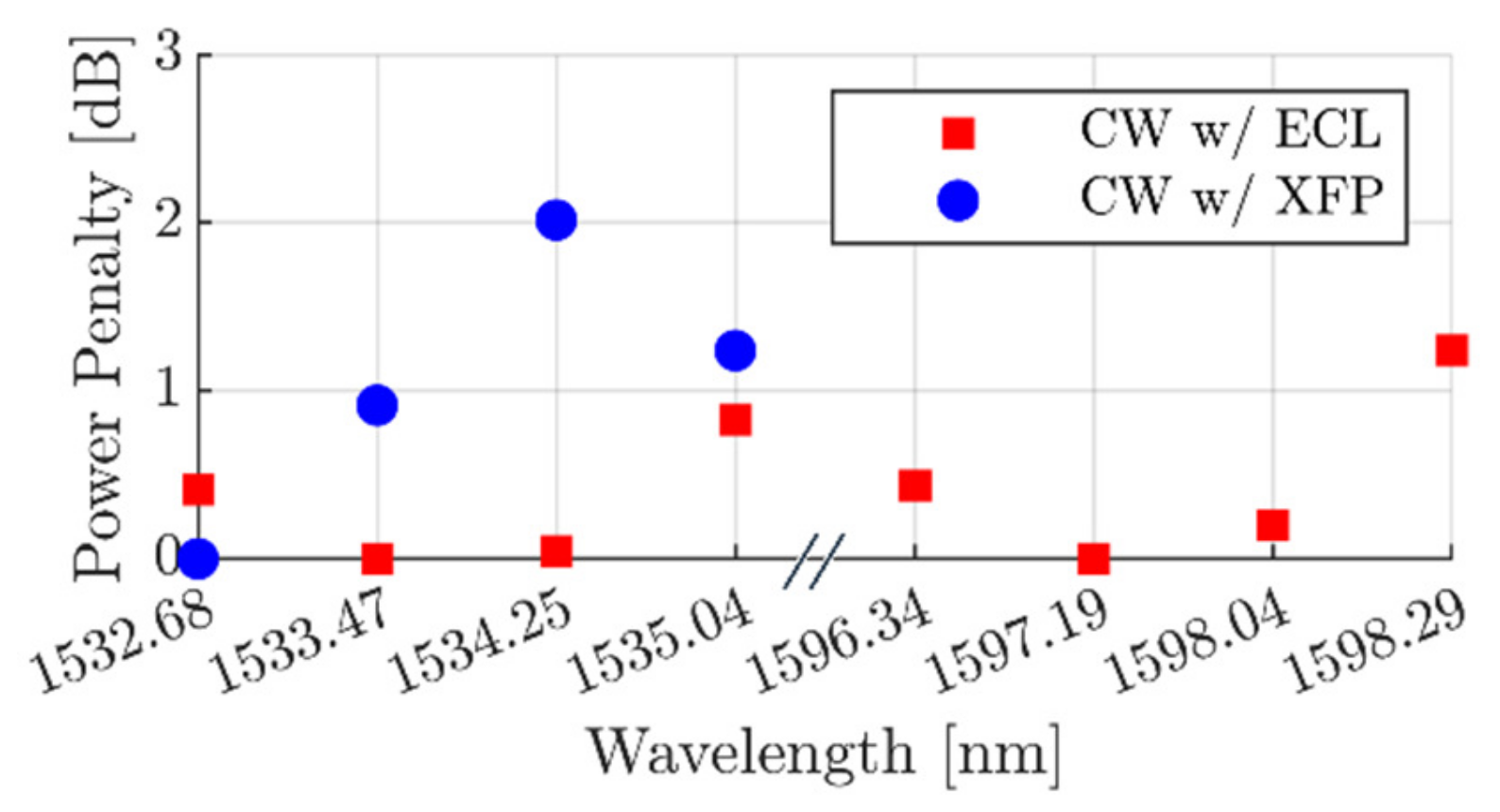
| NGPON2 | 1532.68 | 9.953 | 9 Type A | −28 BER 10E-3 | Ramp up | 1596.34 | 9.953 | 7 N2 | −28 BER 10E-3 | Ramp up | |
| 1533.47 | 1597.19 | 9.953 | |||||||||
| 1534.25 | 1598.04 | 9.953 | |||||||||
| 1535.04 | 1598.89 | 9.953 | |||||||||
| 50G | UW1–Wide | 1290–1310 | 49.764 | 9 N1 | −24 BER 1E-2 | Lab trials | 1340–1344 | 24.883 | 5.5 N1 | −24.5 BER 1E-2 | Lab trials |
| UW2–Wide | 1260–1280 | ||||||||||
| Reference No. | Transceiver Type | Integration | Technology | Target Equipment |
|---|---|---|---|---|
| 80 | Tx | Monolithic | DBR array + SOA + AWG | ONU and OLT (interchangeable) |
| Rx | AWG + array of PIN | |||
| 81 | Tx | Hybrid (InP + Si) | Laser array + AWG + single MZM | ONU |
| Rx | AWG + array of PD per polarization | ONU | ||
| 82 | Tx | Monolithic | Laser array (80 mW output power) | ONU or OLT |
| 84 | Rx | Monolithic | Quasi-coherent | ONU |
Disclaimer/Publisher’s Note: The statements, opinions and data contained in all publications are solely those of the individual author(s) and contributor(s) and not of MDPI and/or the editor(s). MDPI and/or the editor(s) disclaim responsibility for any injury to people or property resulting from any ideas, methods, instructions or products referred to in the content. |
© 2023 by the authors. Licensee MDPI, Basel, Switzerland. This article is an open access article distributed under the terms and conditions of the Creative Commons Attribution (CC BY) license (https://creativecommons.org/licenses/by/4.0/).
Share and Cite
Rodrigues, F.; Rodrigues, C.; Santos, J.; Rodrigues, C.; Teixeira, A. Photonic Integrated Circuits for Passive Optical Networks: Outlook and Case Study of Integrated Quasi-Coherent Receiver. Photonics 2023, 10, 182. https://doi.org/10.3390/photonics10020182
Rodrigues F, Rodrigues C, Santos J, Rodrigues C, Teixeira A. Photonic Integrated Circuits for Passive Optical Networks: Outlook and Case Study of Integrated Quasi-Coherent Receiver. Photonics. 2023; 10(2):182. https://doi.org/10.3390/photonics10020182
Chicago/Turabian StyleRodrigues, Francisco, Carla Rodrigues, João Santos, Cláudio Rodrigues, and António Teixeira. 2023. "Photonic Integrated Circuits for Passive Optical Networks: Outlook and Case Study of Integrated Quasi-Coherent Receiver" Photonics 10, no. 2: 182. https://doi.org/10.3390/photonics10020182