1. Introduction
Similar to the electronic units employed in different engineering fields, electronic units developed in aerospace industries are exposed to various extreme environmental loads during a mission [
1]. These environments involve launch vibration, on-orbit thermal cycling, and space radiation. Generally, the extreme level of mechanical vibration during a launch campaign is the first major environment that onboard electronics are exposed to during a mission. These loads involve quasi-static loads, sine vibration, random vibration, and shock. Among these, random vibration excitation occurs over a wide frequency band from 20 to 2000 Hz and is one of the main causes of the mechanical failure of spaceborne electronic units [
2]. The probability of fatigue failure in the solder joints of electronic packages increases, owing to the repetitive bending behavior of printed circuit boards (PCBs) under vibration excitation. This can lead to the malfunctioning or failure of electronics, and in extreme cases, the failure of the spacecraft.
Various fatigue life prediction approaches based on fatigue failure theories have been studied to enhance the structural safety of solder joints against vibration-induced fatigue failure [
3,
4,
5]. However, most of these approaches are based on the detailed finite element (FE) modeling of the various types of electronic packages. Additionally, although these modeling techniques detail the actual configurations of the packages and solder joints, they are time-consuming. This is because the construction and computation of the FE models of the electronic unit grow cumbersome as the number of packages and their types increase. A more fundamental problem is the difficulty in acquiring all the required accurate information on the material properties, geometry of the solder joint, and internal configuration of the package when they are either absent or kept confidential by the manufacturer. In general, the mechanical design of electronic units requires iterative design and analysis processes based on trade-off studies to obtain a final design that satisfies different development requirements. However, the rapid evaluation of structural safety reduces the number of design trade-off studies, which contributes to the minimization of project resources such as the schedule, manpower, and cost. From this perspective, these time-consuming life prediction approaches based on detailed FE models are not appropriate for the rapid design of spaceborne electronic units with different package types.
As a design methodology for spaceborne electronics, industries and research organizations in the space sector have widely adopted Steinberg’s fatigue failure theory proposed in the 1970s [
6]. This theory guarantees more than 2 × 10
7 fatigue cycles for solder joints exposed to random vibration when the maximum PCB dynamic displacement is limited to lower than the allowable value calculated using Steinberg’s empirical formula. The concept of this theory allows the use of simplified modeling techniques for electronic packages because the board displacement is calculated with reasonable accuracy, even if the package configuration in the FE model is not sufficiently detailed [
7,
8]. However, Steinberg’s formula was created with the assumption that PCBs are rectangular-shaped and have a simple half-sine mode shape under simply supported boundary conditions. Therefore, if a PCB has a complex distorted mode shape, this assumption causes an estimation error in the margin of safety (MoS) of solder joints due to the asymmetric board shape and irregular positions of the fixation points. Another problem is that the criterion of 2 × 10
7 fatigue cycles for random vibration creates a huge margin between the fatigue life of solder joints and the total number of cycles accumulated during the vibration tests and launch. These are the major issues related to the structural overdesigning of the electronic unit.
In response to these limitations, Park and Oh [
9] proposed a critical strain-based structural design methodology called “Oh–Park methodology” to evaluate the structural safety of solder joints in spaceborne electronic units based on the critical strain theory. Its key approach is to evaluate the structural safety of solder joints based on a MoS calculation with respect to the PCB strain and considering random vibrations that occur during launch. In addition, the
MoS can be calculated in accordance with the required time to failure (
TTFreq) for the survival of solder joints in on-ground vibration tests and during launch. These approaches mitigate the limitations of Steinberg’s theory such as the unreliable structural safety evaluation and possibility of structural overdesign. Park and Oh [
9] proposed simplified FE modeling techniques for the ball grid array (BGA) and column grid array (CGA) packages, which only consist of a zero-dimensional (0D) lumped mass and rigid link elements. This technique effectively reduced the time and effort required to model the package while being reasonably accurate at evaluating the solder joint’s structural safety. For evaluating the effectiveness of the Oh–Park methodology, plastic BGA and ceramic CGA package specimens with various PCB boundary conditions were fabricated and exposed to random vibration excitation. Using a comparison of the
MoS of the solder joints and TTF of the tested specimens, they proved that the results of their proposed method were consistent with the test results. In contrast, Steinberg’s theory generally yielded invalid results for these specimens.
In a previous study [
9], the Oh–Park methodology was validated only for the area array packages of the BGA and CGA. However, lead frame packages such as the small outline package (SOP) and quad flat package (QFP), wherein the lead frames and solder joints are arranged along the outer perimeter of the package body, have also been widely used in spaceborne electronic units. The gull-wing-shaped configuration of the lead frame array provides increased mechanical flexibility compared with the solder joints of area array packages. This configuration reduces the thermal deformation and vibration-induced stress acting on the solder and lead frame itself. However, the lead frame package is still vulnerable to fatigue failure in the solder joint when exposed to high-vibration-induced board deflection. To increase the completeness of the Oh–Park methodology in the structural design of spaceborne electronic units, further verification using lead-frame types of packages is required in addition to those considered by Park and Oh in [
9].
The aim of this study is to validate the effectiveness of the Oh–Park methodology in evaluating the structural safety of SOP solder joints; this has not been previously investigated. One important goal of this study is to find a feasible simplified FE modeling technique for SOPs by using the 0D lumped mass and rigid link elements. This form of modeling has not been proposed for SOPs in previous studies. The elements used in this model are so simple that it is advantageous for saving significant time and effort to model the package rapidly. The new FE modeling technique for SOP is the core of the novelty of this study. A total of 48-pin thin SOP (TSOP48) specimens are fabricated and mounted on PCBs under various boundary conditions before being exposed to random vibration excitation on a vibration shaker. The time to failure (TTF) of the tested packages is then compared with their MoS values, which are calculated using the Oh–Park methodology and based on various forms of simplified FE modeling techniques. The proposed method is also compared with the conventional Steinberg’s theory. The verification results indicate that the application of the Oh–Park methodology using the proposed FE modeling technique is a feasible method for evaluating the structural safety of SOP solder joints.
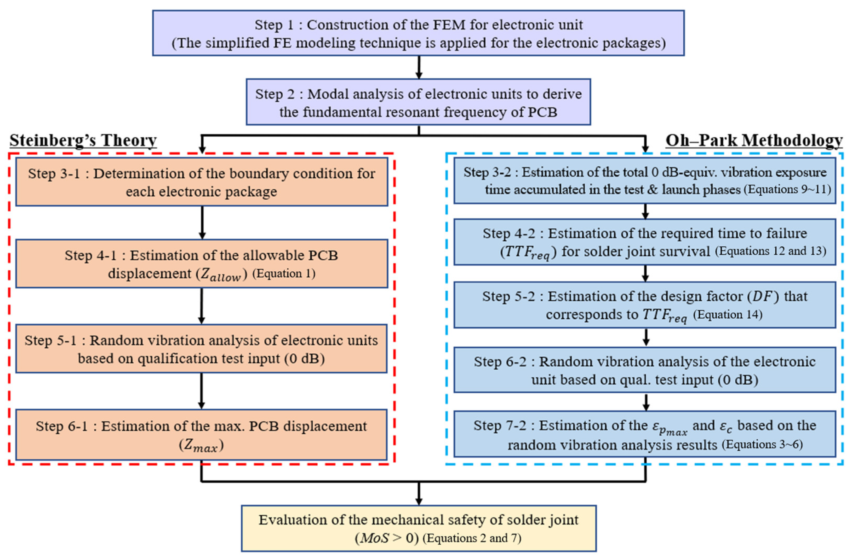
2. Structural Design Methodologies
Figure 1 shows the structural design processes using the Oh–Park methodology and Steinberg’s theory for spaceborne electronic units. The major equations that constitute these methodologies are described throughout this chapter to describe their theoretical differences.
In the first step of evaluation (Step 1), the FE model of the electronic units is constructed by applying the simplified FE modeling techniques for the various types of electronic packages such as the BGA, CGA, and lead frame packages. The electronic package FE modeling techniques are detailed in
Section 4. In Step 2, the modal analysis of the constructed FE model is performed to identify the fundamental PCB modes with respect to the different locations on the board where each package is mounted.
Steps 3–1 to 6–1 describe the design evaluation process using Steinberg’s theory. In Step 3–1, the modal analysis results obtained in Step 2 are used to find the mode that is most relevant to the maximum dynamic response of the board at the package mounting position. This is the most important process to properly estimate an allowable PCB displacement
for the package in Step 4–1 using Equation (1) shown below [
6]:
where
is allowable PCB displacement [in.] (converted to mm after estimation).
is length of the PCB boundary parallel to the package [in.].
is constant for the electronic packaging type.
is PCB thickness [in.].
is relative position factor of the package on the PCB calculated by geometric factors
,
,
, and
defined in
Figure 2a. Here,
or
value becomes the value of a length of PCB parallel to the package
[in.].
is package body length [in.].
In Step 5–1, random vibration analysis is performed on the electronic unit using the input random spectrum equal to the qualification test’s full level (0 dB). In Step 6–1, the analyzed maximum PCB displacement (
) for each package, which is the three-sigma (3σ) value of the root mean square (RMS) displacement, is obtained at the PCB location underneath the center of the package body defined as shown in
Figure 2b. In the final step,
of the solder joint is calculated for each package based on
and
using Equation (2) described as follows:
where
is factor of safety for
MoS calculation. The
values such as 1.11, 1.25, and 1.4 have been used for
MoS calculation in previous studies [
7,
10,
11,
12]. Applying
values to the stress yields the
in terms of the fatigue life and in accordance with the stress-life cycle curve (
-
curve) described as follows [
13]:
where
is the fatigue exponent of the solder or lead frame material of the package. Steinberg [
6] assumed that the stress or strain of the solder joint is proportional to the board displacement (
). Therefore, this relationship is also valid for
, as described in Equation (3). In general, the Sn-Pb37 solder material has been widely used in spaceborne electronic units. For high cycle fatigue such as vibration, the value of
is typically taken as 6.4 [
6]. The ECSS rule [
14] recommends using
= 4.0 or higher for the fatigue. For example, if the Sn-Pb37 solder is used in a package, the corresponding
of
is approximately 1.25, according to Equation (3). These aspects were reflected to determine the
for evaluating the solder joint safety of a selected SOP specimen that is described later. If the estimated
is greater than or equal to zero, at least 2 × 10
7 fatigue cycles for random vibration is guaranteed for solder joint according to the Steinberg’s criterion.
The theoretical limitations of Steinberg’s theory are mainly owing to
B and
r in Equation (1). These factors can be clearly estimated only when the mode shape is an ideal half-sine wave, like that shown in
Figure 2b. The occurrence of an error in the estimated
is inevitable if the mode shape strays from the assumption. This implies that Equation (1) cannot explain the complex mode shapes caused by the asymmetric mechanical design configuration of electronic units. A similar problem occurs in the case of
owing to the aforementioned limitation. This is because the proportional relationship between the board displacement and actual stress on the solder joints, assumed by Steinberg, can be invalid if the board is distorted in a complex manner.
Another technical problem in Steinberg’s theory is the production of an overly conservative design criterion that causes structural overdesigning of electronic units; this was reported in a previous study [
7]. Steinberg’s criterion of 2 × 10
7 fatigue cycles imposes a very high margin on the fatigue life of the solder joints of spaceborne electronic units, which are typically exposed to vibrations for several tens of minutes in on-ground vibration tests and during launch. Generally, the PCB assembly is designed to achieve the fundamental resonant frequency from 100 to 1000 Hz [
7,
8,
9,
10,
15]. Assuming that
is greater than zero, the criterion of 2 × 10
7 fatigue cycles can increase the solder joint fatigue life by several hours, even if the board resonant frequency goes higher than 1000 Hz. This conservatism becomes more aggravated when
is applied in the
calculation. The root cause of this issue is the use of Steinberg’s criterion even though it was not originally established for spaceborne electronic units in the first place. In other words, prior to the study conducted by Park and Oh [
9], no other suitable design criteria were developed for spaceborne electronic units. The recent New Space paradigm requires the development of lighter and smaller satellites. In this context, one of the core mechanical design strategies is to reduce the structural overdesigning of onboard electronic units that occupy a large mass and volume in the satellite. Thus, a new design criterion for spaceborne electronic units is required to substitute that proposed by Steinberg.
As mentioned earlier, to overcome the theoretical limitations of Steinberg’s theory, Park and Oh [
9] proposed a new mechanical design methodology called the Oh–Park methodology for spaceborne electronic units. Unlike Steinberg’s theory, the Oh–Park methodology evaluates the solder joint safety based on the
calculation with respect to the critical PCB strain on the electronic package. The use of the board strain enables the feasible evaluation of solder joint safety even if the PCB exhibits complex distorted mode shapes. In addition, it resolves the overdesigning problem caused by Steinberg’s design criterion because the solder joint safety is evaluated considering the
for survival in the vibration test and during launch processes.
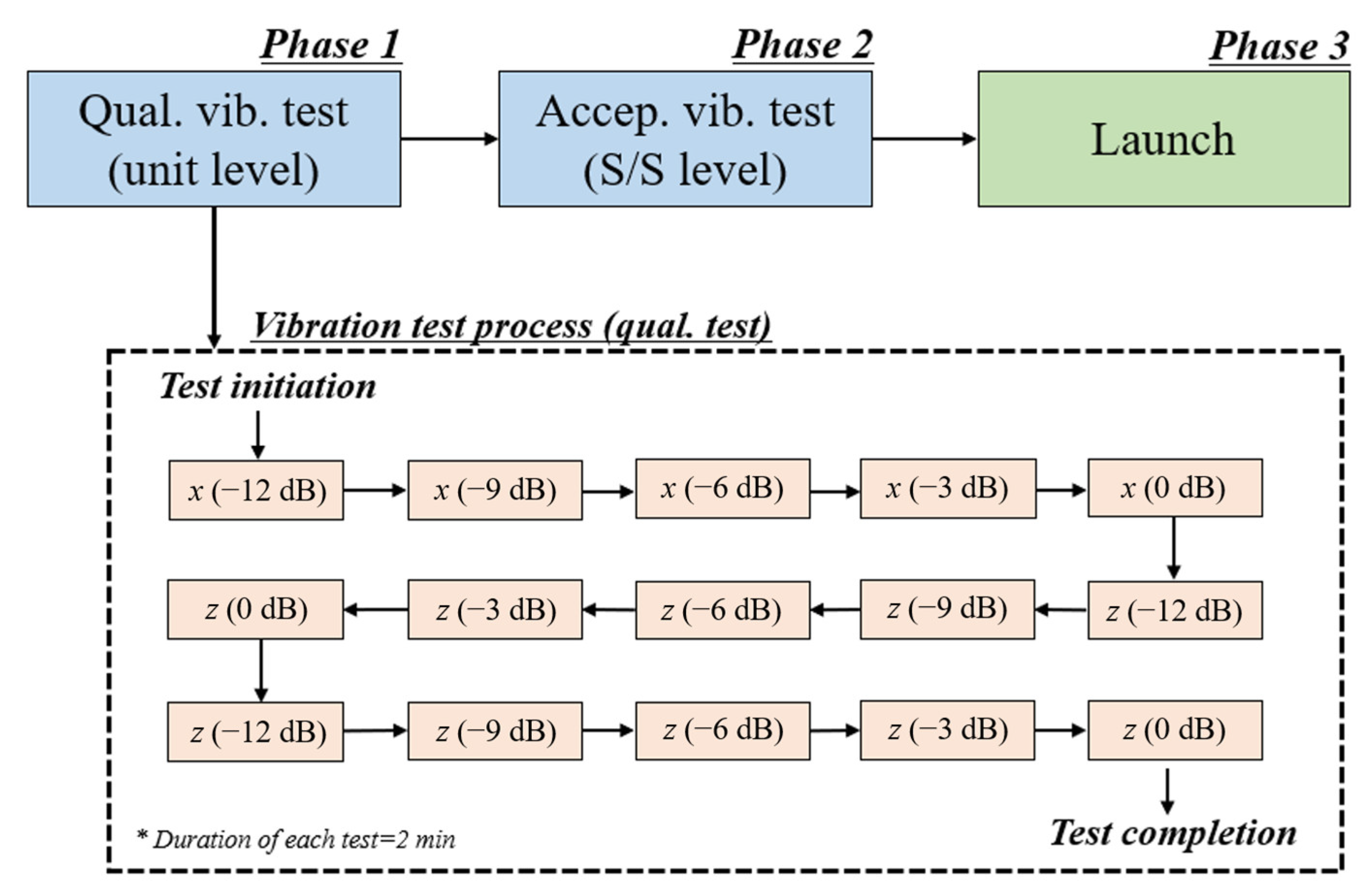
The Oh–Park methodology is employed to evaluate the solder joint safety based on the design process in Steps 3–2 to 7–2, as described in
Figure 1. In Step 3–2, the total vibration exposure time in the vibration test and during the launch processes is estimated. In this study, the effectiveness of the Oh–Park methodology was evaluated based on an example of the test and launch processes for satellite onboard units, as described in
Figure 3. In this scenario, only a single electronic unit is assumed to be manufactured and subjected to qualification test phases at the unit level and flight acceptance tests at the satellite system level and during launch to reduce the cost and schedule. Here, the qualification test phase includes random vibration tests with five steps for each axis and a gradual increase in the input levels from −12 to 0 dB (qualification full level) with +3 dB increments. The 0 dB level was excluded from the acceptance test, and the rest of the processes were the same as those of the qualification test. An entire launch campaign typically lasts between tens of minutes and several hours; however, the major random vibration occurs in the first few minutes after lift-off when extreme aerodynamic pressure is acting on the launcher. Accordingly, the launch random vibration duration was assumed to be 4 min, and simultaneously, the excitation equivalent to the acceptance test level was generated in 3 axes.
Generally, a mechanical design evaluation of the electronic units is performed to prove the structural safety with respect to the qualification-level random vibration (0 dB). Therefore, all the load levels in the test and launch were substituted to a 0 dB-equivalent exposure time for random vibration, using the Equation (4) described as follows:
where
and
are the exposure times of an individual vibration test and launch, respectively, and
is the fatigue exponent of the solder or lead material. Additionally,
is the ratio of the RMS input test level to the 0 dB input, which is described as follows:
where
is the number of tests for each axis. Here, it is assumed that the solder joint fatigue equal to that of the PCB out-of-plane excitation is accumulated in all the test axes of the electronic unit. Therefore,
= 3 was used for estimation in the 3-axis tests. This assumption simplified the estimation and generation of conservatism on solder joint safety to some extent.
A total 0 dB-equivalent exposure time can be estimated for a single test phase from the summation of the
values for each test level derived using Equations (4) and (5). For the unit-level qualification test, the accumulated 0 dB-equivalent vibration exposure time,
, can be described as follows:
In Step 4–2, the
for the solder joint is estimated from the summation of the accumulated exposure time during the entire test phase and launch phase using Equation (6) described as follows:
where
is an accumulated 0 dB-equivalent vibration exposure time in the vibration test or launch phase.
is a factor of safety for
. In this study, an
value of 4.0, which is the recommended value for fatigue based on the ECSS standard [
14], was used for the estimation. The
for the scenario displayed in
Figure 3 is estimated as follows:
where
and
are the accumulated 0 dB-equivalent vibration exposure times in the acceptance test at the spacecraft system (S/S) level and launch phases, respectively.
In Step 5–2, the design factor,
, is estimated based on
and
estimated in Steps 2 and 4–2:
where
is an original Steinberg design criteria (2 × 10
7 cycles) for solder joint survival when exposed to random vibration,
is the total number of fatigue cycles for solder joint survival, and the
is estimated for each package.
In Steps 6–2 to 7–2, the maximum in-plane principal PCB strain
is estimated for each package by using the RMS strain components derived from the random vibration analysis of the electronic unit using Equation (10) described as below:
where
and
are
x and
y normal strain components of the PCB [μ-strain], respectively.
is
xy shear strain component of the PCB [μ-strain]. The
is then used to estimate PCB strain rate
[μ-strain/s], allowable PCB strain
[μ-strain] and critical PCB strain
[μ-strain] using Equations (11)–(13) described as below:
where the factors
,
and
are the same as those defined in Steinberg’s theory. Finally,
is calculated by using
,
, and
, using Equation (14) described as follows:
where
is estimated by Equations (4)–(9). The design criterion of Oh-Park methodology is that
for random vibration is guaranteed when the estimated
is greater than or equal to zero.
Those three factors of , , and are key elements used to utilize the main advantages of the Oh-Park methodology. Substituting Zallow and into the and in the calculation overcomes the theoretical limitations of Steinberg’s empirical formula, which leads to a reliable evaluation of solder joint safety. The overdesigning issue in Steinberg’s design criterion can also be resolved by estimating and using a suitable that reflects the solder joint fatigue life for a specific test and launch plan.
In the space engineering field, the peak responses of acceleration, displacement, stress, and strain in random vibration are commonly considered as 3σ values of RMS response under the assumption that the peak responses follow the Gaussian probability distribution. In accordance with Gaussian distribution, most of the fatigue damage is generated by peak responses up to the 3σ level [
6]. This is because the response will be within a −3σ~+3σ range for 99.73% of random vibration duration. The use of the 3σ value for evaluating structural safety is one of the common standards in the space industry. Those are the reasons why we applied the maximum peak value of
as the 3σ value of RMS in-plane principal strain. However, the peak response for Gaussian stationary random vibration is almost always greater than 3σ in most of the cases. Nevertheless, even if the peak responses at 4, 5, and 6σ levels are involved in the estimation, the total consumed fatigue life is increased by only 28.13% compared with that calculated by involving up to the 3σ level. This can be observed by calculation using a Miner’s cumulative damage cycle ratio equation with a principle of a three-band technique [
6]. This percentage does not change even if
,
, and stress level are changed. This means that the above calculation is valid in different boundary conditions of structure and enforced vibration conditions. Based on these assessments, maximum peak responses exceeding 3σ level were ignored in this study because their portion in the fatigue life is relatively much smaller than
= 4.0 (400% margin) included in the
for
calcualation. These assessments give a justification to use the 3σ level of RMS in-plane principal strain as
involved in MoS estimation.
3. Fatigue Life Tests on the PCB Specimens
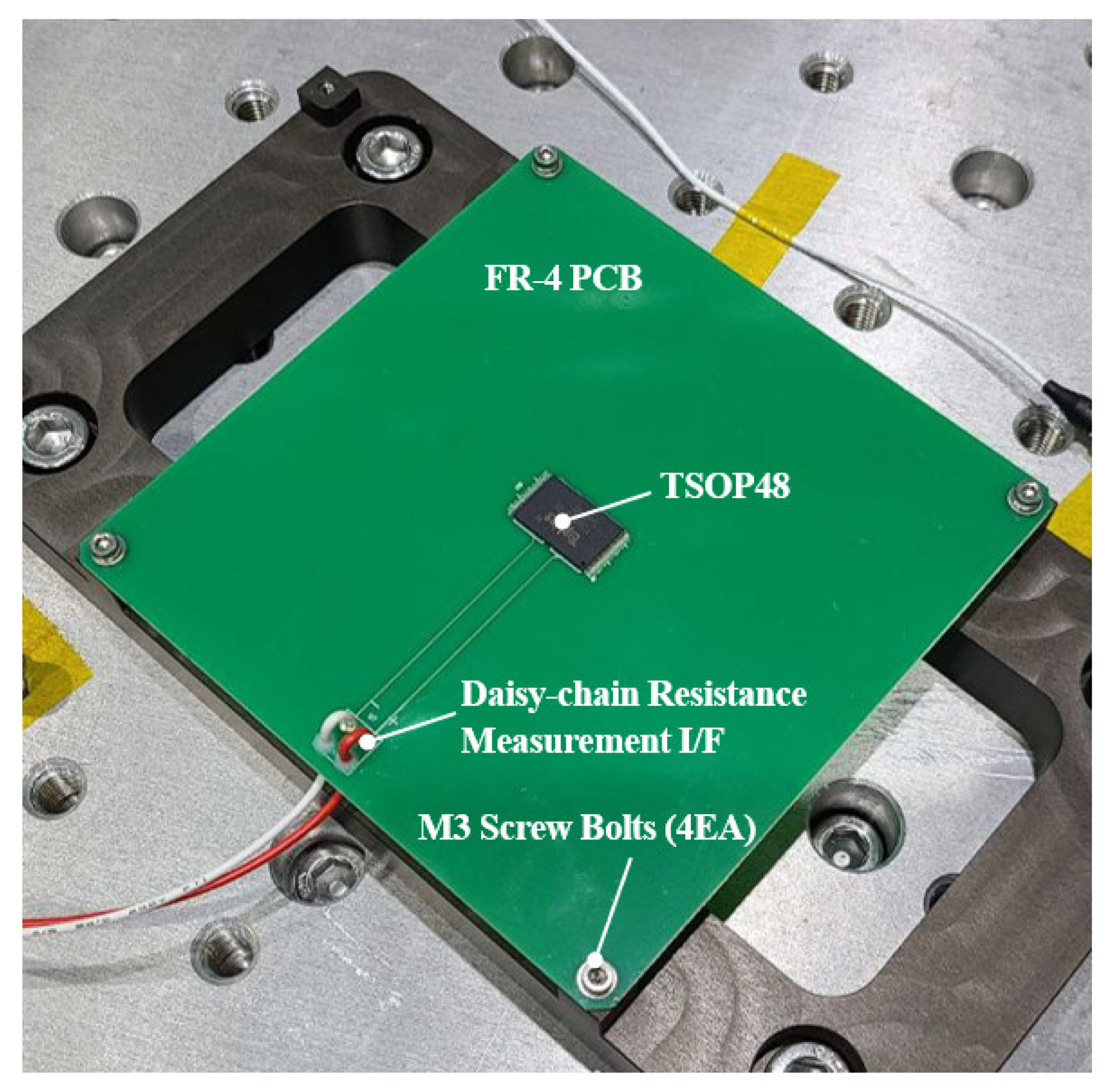
As mentioned earlier, to validate the Oh–Park methodology for the SOP, a 48-pin plastic SOP (TSOP48) was selected and assembled on PCB specimens to perform fatigue life tests under random vibration. The representative configuration of the PCB specimen in Case 1 is depicted in
Figure 4, and
Table 1 shows the specifications of TSOP48. The PCB consists of a two-layer FR-4 laminate with an area of 135 mm × 135 mm and a thickness of 1.6 mm. Additionally, the weight of the PCB assembly is 54.5 g, and the PCB is constrained using four M3 screw holes.
Figure 5 shows an example of a daisy-chain circuit for TSOP assembled on the PCB. This form of electrical connection, where all the lead frames are connected in a series, makes it easier to detect crack initiation in the solder joint or lead frame during the vibration test, simply by monitoring the two-wire resistance of that circuit.
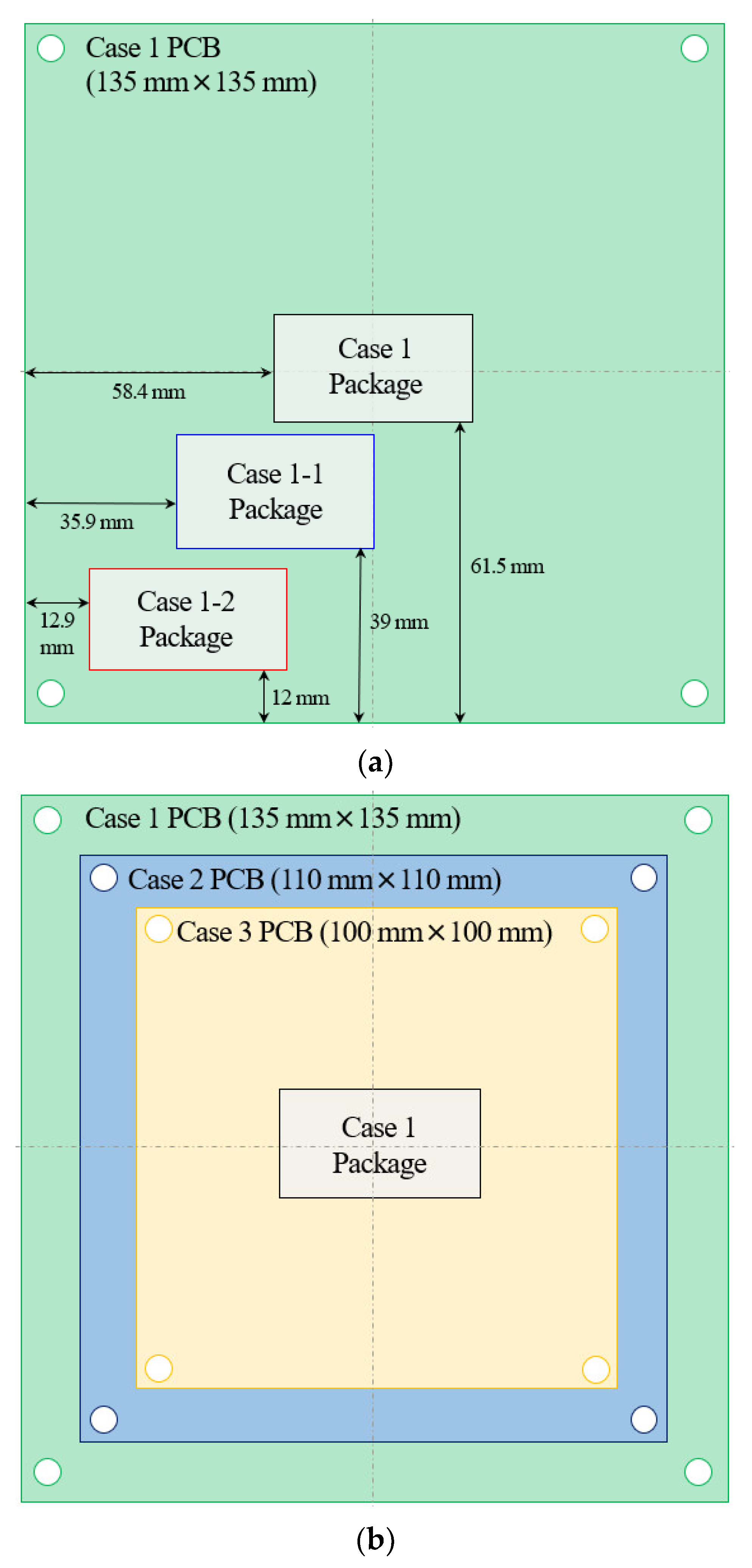
Five PCB specimen cases were fabricated to validate the Oh–Park methodology for the SOP type according to various boundary conditions, as shown in
Figure 6. These specimen cases involve various mounting locations of packages on the board (Cases 1, 1–1, 1–2) and various board sizes (Cases 2, 3). In Case 1–2, the package is located adjacent to the screw joint at a distance of 10 mm, wherein the board strain caused by the screw constraint influences the package. The main intention of establishing five cases of PCB specimens, as those shown above, is to verify the effectiveness of the proposed methodology for use in various design cases. This is because the PCB size and package mounting location are major factors that are frequently changed in the design trade-off of electronic units. In this study, two sets of test specimens were prepared and tested to ensure the reliability of the test results.
Figure 7 shows the representative fatigue life test setup, where Case 1 of the PCB specimens is mounted on an electrodynamic shaker. The
TTF of each package was measured by applying 2-wire resistance logging and monitoring, which was performed by using a DAQ6510 (Keithley Co., Ltd., Solon, OH, USA) data acquisition (DAQ) device. As per the IPC-9701A standard [
16], the solder joint fails when a daisy-chain resistance value that is 20% higher than the initial value is consecutively detected five times.
Table 2 shows the random vibration input specifications of the fatigue life test, wherein 20 Grms of random vibration were continuously applied to the test specimens until the failure criterion was reached.
Figure 8 shows the time histories of the daisy-chain resistance values of the first set of test specimens. Here, the first failure of the solder joint is detected after 9.22 min of random excitation in the Case 1 specimen. Subsequently, Case 3 fails after 13.0 min of excitation, and Cases 2 and 1–1 fail after approximately 20 min. Case 1–2 survives the longest among the specimen cases and finally fails after 113.45 min of exposure.
Table 3 summarizes the measured time to failure,
, of all tested specimens. The overall test results show that the time to failure of the solder joints tends to increase higher than that of Case 1 with an increase in the position of the package from the center of the PCB and with a decrease in the board size. It was observed that the change in package mounting position is more effective to increase the time to failure as compared with the increase in fundamental resonant frequency (
) of PCB by reducing the board size. The
of the PCB specimens in each case show a similar tendency in Sets 1 and 2, although there are some differences. These test results were used to validate the Oh–Park methodology for the SOP.
4. Verification of the Structural Design Methodology
Figure 9 shows the evaluation process used to determine which structural design methodology is more reliable in estimating the structural safety of the SOP solder joint. The FE modeling guideline for the SOP was set up by employing a trial-and-error approach through repetitive structural analyses based on the PCB modeling technique proposed by Park and Oh [
9]. Consequently, three types of simplified modeling techniques were proposed for the SOP. Each analysis case had a different modeling technique, and solder joint safety evaluation was performed using the Oh–Park methodology and Steinberg’s theory according to the analysis process described in
Figure 1. The evaluation criterion used to judge the effectiveness of the methodology is whether the estimated
MoS values accurately represent the average
of the tested specimens. In this study, the
is predicted based on two methodologies to investigate whether the calculated
MoS values accurately represent the
of the tested packages. The predicted
(
) is estimated based on the PCB displacement using the power-law-based equation, described as follows:
where
is 2 × 10
7, being the number of cycles for random vibration. Based on the PCB strain,
is calculated as follows:
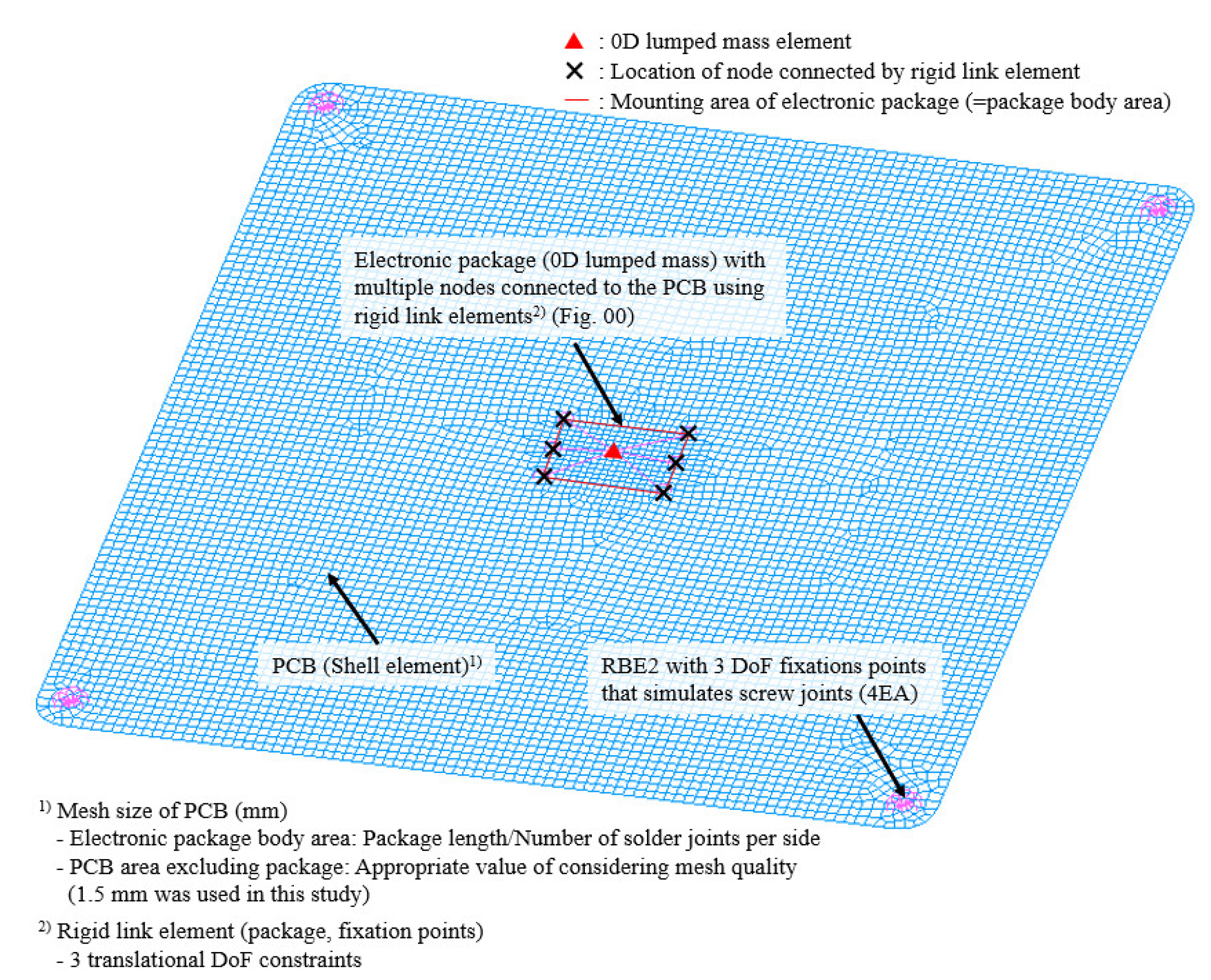
Figure 10 shows a representative FE model for the Case 1 specimen with Type 2 modeling of the SOP. The PCB was modeled using the first-order shell element of QUAD4 because it is more efficient in predicting the in-plane strain of a plate structure like PCB compared with the solid element in terms of the minimization of the mesh density. The area of the PCB occupied by the package body is uniformly meshed and the mesh size is the same as the lead frame pitch (0.5 mm) of the package. The rest of the board area has a 1.5 mm mesh size. The fixations by using bolt screw joints were simulated by using rigid link elements with mechanical constraints in three translational degrees-of-freedom (DoFs), where the independent node was located at the center of the screw hole, and six DoFs were constrained. These PCB modeling techniques are similar to those proposed by Park and Oh [
9].
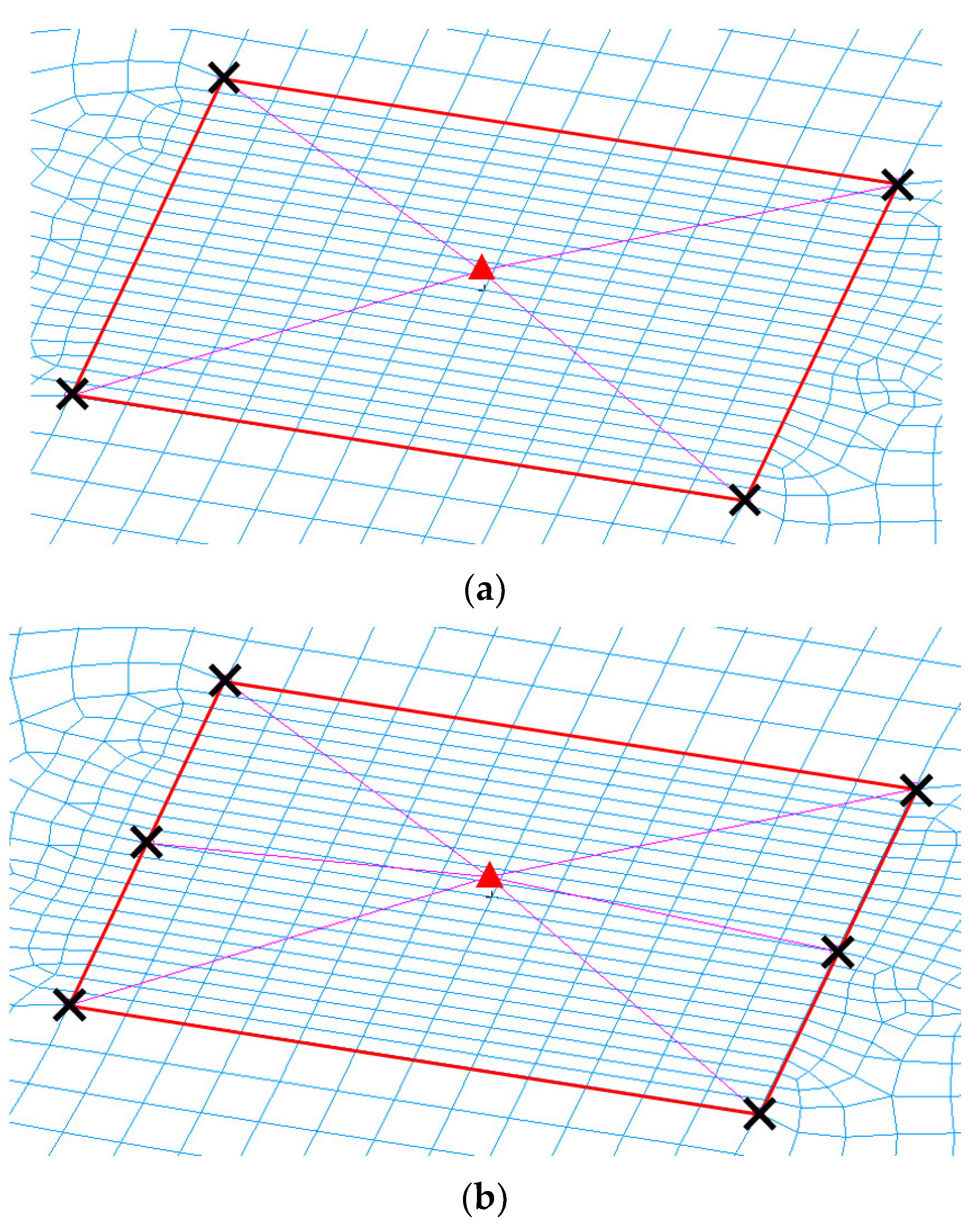
Figure 11 shows the close-up views of the proposed FE modeling techniques for SOP. In this study, the package was modeled with a 0D lumped mass to simulate the package mass and rigid link elements in the solder joint simulation. The main feature of the SOP configuration was implemented in the FE modeling. The SOP-type leaded package has two lines of gull-wing-shaped lead frames at two opposing sides of the package body, as shown in
Table 1, unlike the BGA and CGA packages, which have solder joints in the area arrays. To reflect these features in the modeling, the rigid link element was connected only to the nodes at the two opposing side edges of the package body area to simulate the package–board connections using lead frame solder joints. Types 1, 2, and 3 modeling correspond to the case where the connection points on the rigid link elements are four, six, and ten nodes, respectively, as shown in
Figure 11a, b, and c, respectively. This form of modeling has not been proposed for SOPs in previous studies despite being extremely simple and consuming significantly less time and effort than model multiple packages. This contributes to the rapid model construction of electronic units using various types of packages, which is one of the important advantages of the Oh–Park methodology.
As the number of rigid link connection points is increased, the dynamic strain response of PCB at the corner-most points in the package mounting area is reduced by strain dispersion to the adjacent connection points. Therefore, the analyzed value could be excessively lower to estimate the , and vice versa. Our approach to finding a valid FE model was the repetitive analysis of candidate models to find a proper number of rigid link connections for the package that produces a minimum error in estimating of the solder joint.
Figure 12 shows the estimation method for
from the random vibration analysis results.
is calculated using Equation (10), and the RMS nodal strains
,
, and
are extrapolated from the element centroids. The RMS nodal strain is the average value of the strains at the four nodes in the corner-most QUAD4 element of the PCB package mounting area. All the modeling and analysis approaches described in this paper are part of the Oh–Park methodology.
After the FE models of the PCB test specimens were constructed by using the three different modeling techniques, modal analysis was performed for each case.
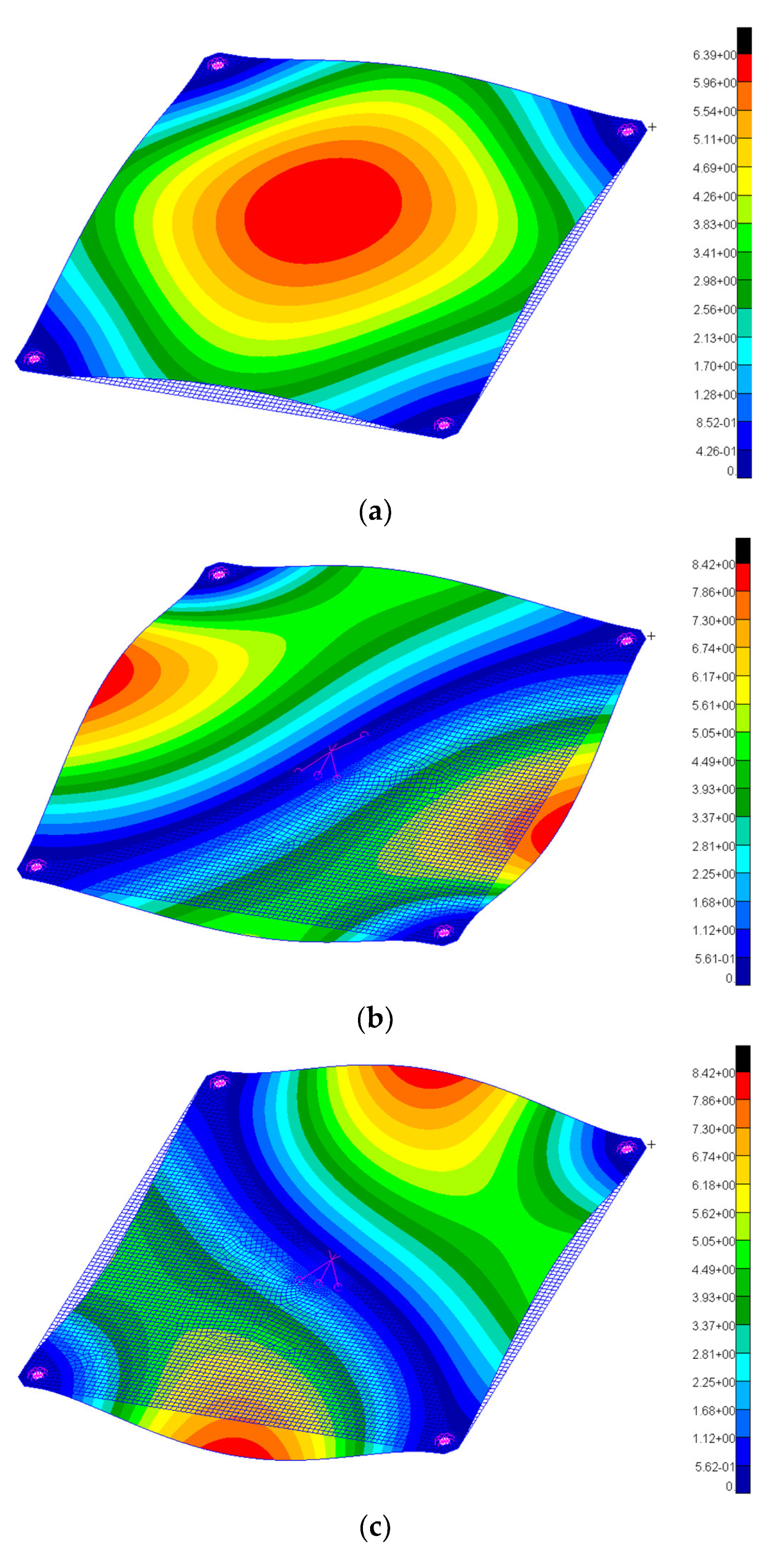
Figure 13 shows the representative results of the first three major mode shapes of Case 1 of the PCB specimen constructed via Type 2 modeling.
Table 4 summarizes the analyzed
for the five cases of tested PCB specimens modeled using the Type 1, 2, and 3 techniques.
Table 5 summarizes the
estimation results for solder joint survival in the assumed development scenario shown in
Figure 3. The estimation was performed using Equations (4)–(8). The estimated
value is 35.2 min, which was used as the design criterion for the electronic unit. For the
calculation,
DF was estimated using Equation (9) by applying the analyzed
and
.
Table 6 indicates the estimated
for the tested specimens using the Oh–Park methodology and Steinberg’s theory when the Type 1 FE model is applied.
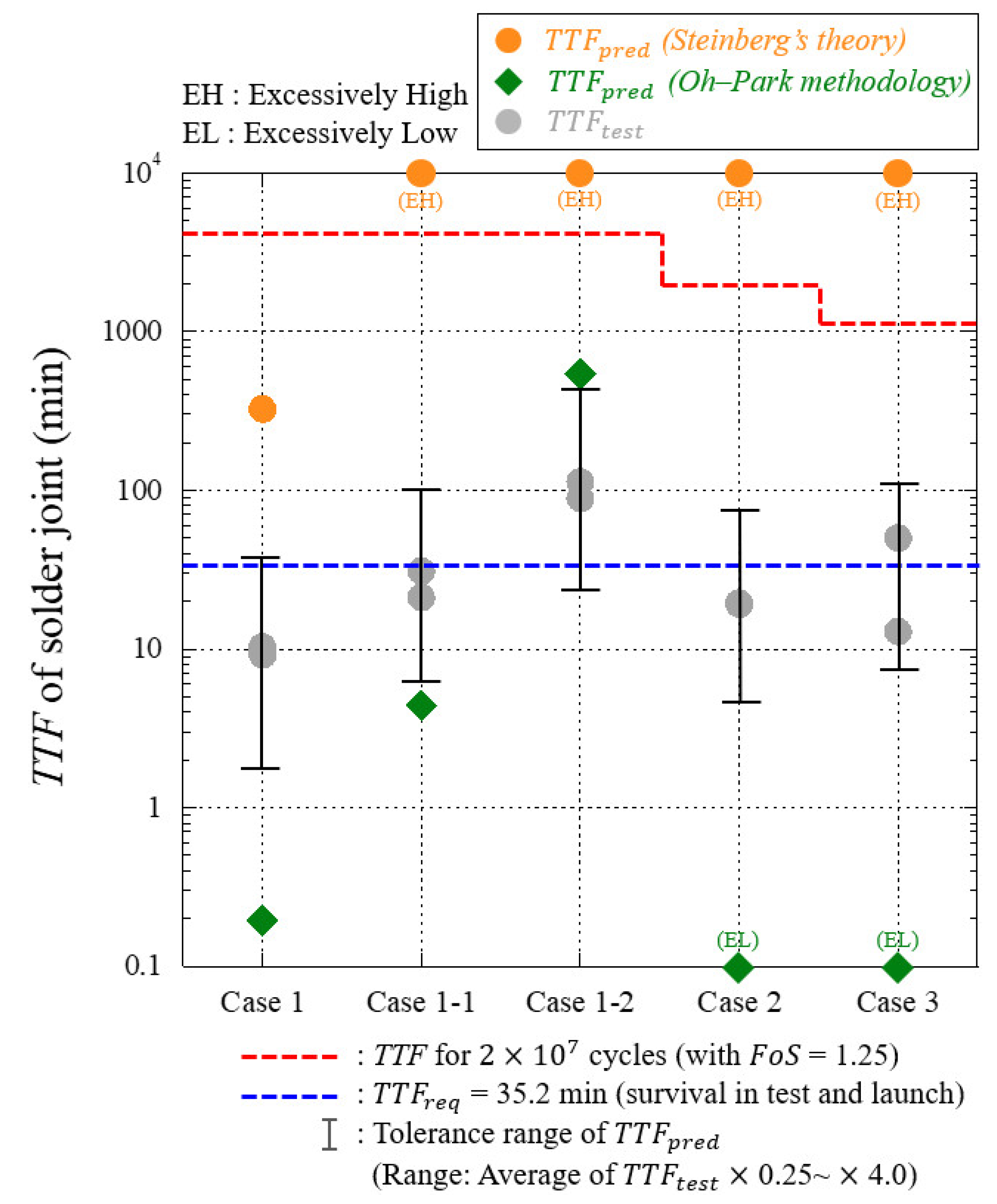
Figure 14 shows a comparison of
and
values estimated by using both methodologies. For the evaluation,
= 1.25 was selected and applied in the
calculation for TSOP48 comprising an Sn-Pb37 solder and copper lead frame considering
= 6.4 according to the relation described in Equation (3). The blue dotted line plotted in the figure is
= 35.2 min, derived in the assumed test and launch scenario summarized in
Table 5. This line becomes a criterion for judging the reliability of predictions based on the design methodologies. It helps to understand whether
well agrees with
in each specimen case. The effectiveness of the design methodologies was evaluated based on the estimated
and
values plotted in the figure. If both
and
values are larger or smaller than the
(above or below the blue dotted line), it can be seen that the prediction well agrees with the test results. In addition, this means that
well represents
.
The analysis results shown in
Table 6 and
Figure 14 indicate that the
and
estimated by using the two methodologies show clearly opposite trends for most of the specimens. The
calculated by using Steinberg’s theory shows invalid results because the Case 1 specimen is the only one with a negative value although the
values of Cases 1, 1–1, 2, and 3 were less than
= 35.2 min. Furthermore, the
of Case 1 is inaccurate because the
, which was calculated based on
instead of
, shows a positive margin, as described in
Table 6. In addition,
values of all the specimen cases were unreasonably higher than the specified error range for
. Meanwhile, the results obtained using Oh–Park methodology show excessively negative
and
values in all the specimen cases when
= 1.25. However, the
values of all cases become reasonable when
is applied instead of
, although their
values are higher than the acceptable error range. The inaccurate
resulted in an excessive value of the analyzed
due to the strain concentration at the corner-most area of the package.
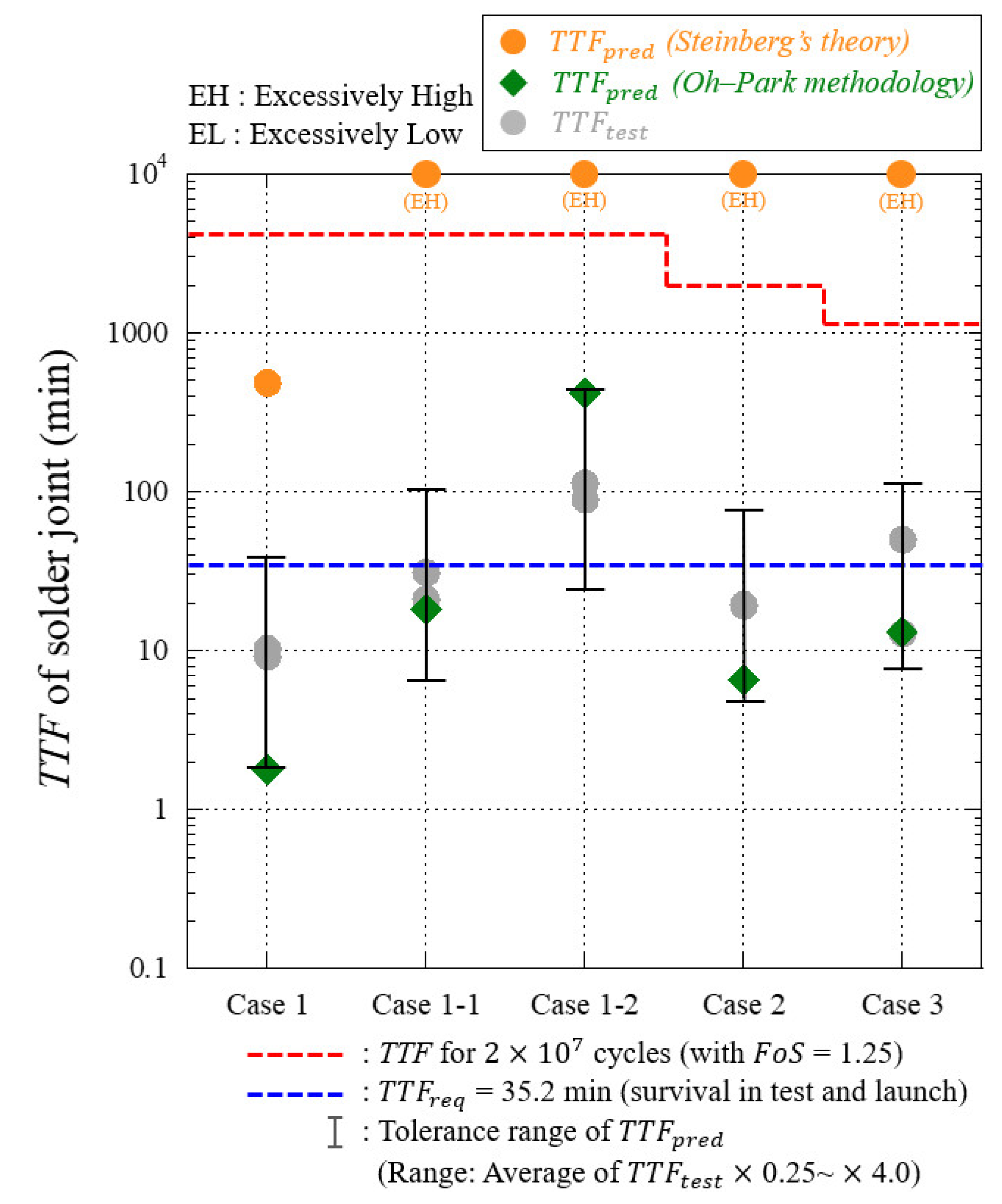
Table 7 summarizes the results of the
calculation for the Type 2 FE model, and the relevant
values are plotted in
Figure 15. Both the
and
calculated by using the Oh–Park methodology represent the
within a specified error range. All results indicate that the structural safety for the
= 35.2 min is evaluated with considerably high accuracy compared with that in the case of the Type 1 model. This is because the strain concentration phenomenon observed in the latter case, as shown in
Table 7 and
Figure 15, is mitigated due to the increased connection points of rigid link elements for the SOP. In contrast, compared with the test data, the
calculated by using Steinberg’s theory still shows excessively positive margins in all cases. The analyzed
values are also significantly higher than those of the test data.
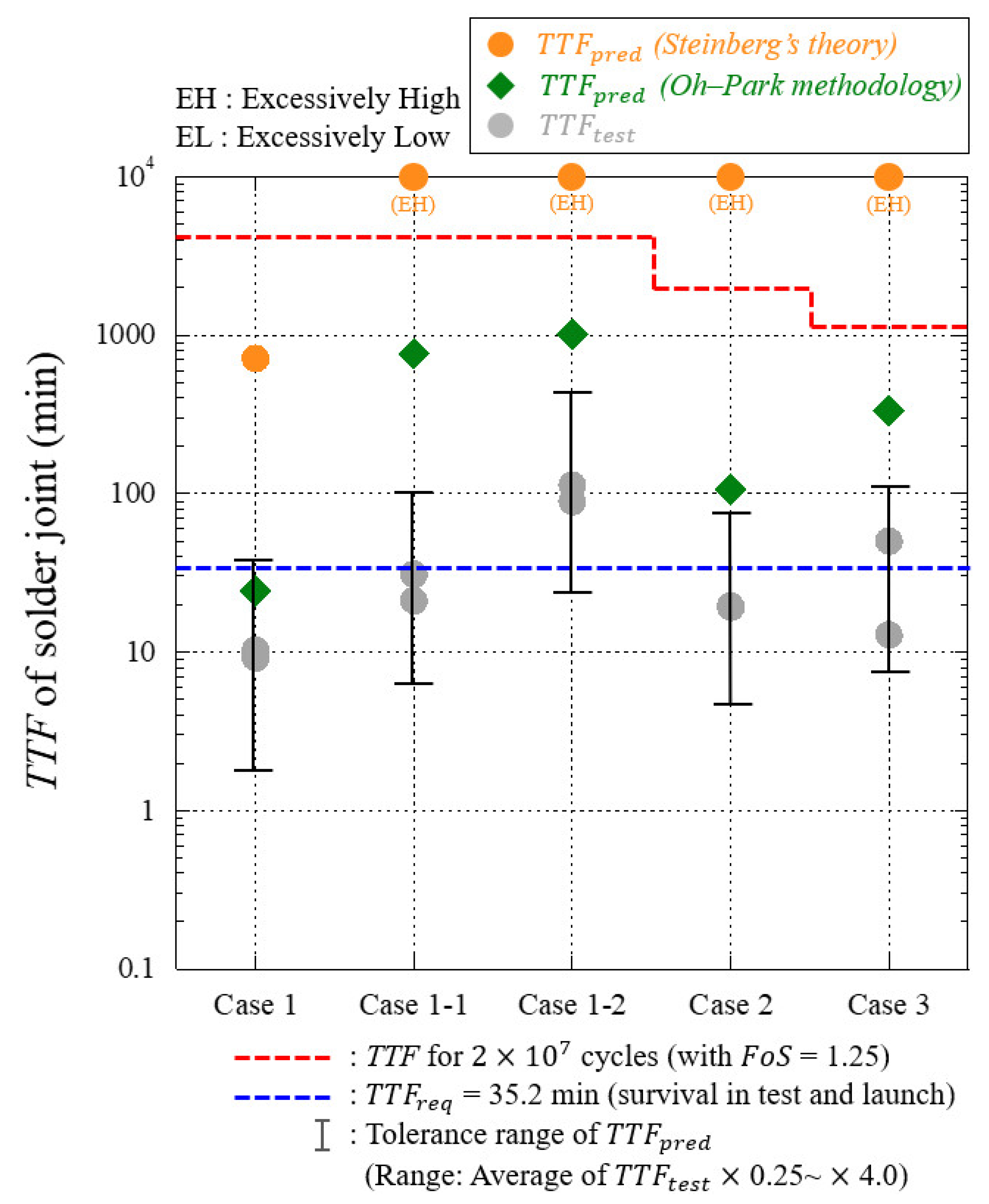
Table 8 and
Figure 16 presents the evaluation results using both design methodologies and based on the Type 3 FE model. The Oh–Park methodology exhibits similar
calculation results. However, the
values are excessively positive beyond the acceptable error range in all specimens except Case 1 because of the significant reduction in the aforementioned strain concentration. This implies that the Type 3 model is less suitable compared with the Type 2 model. Steinberg’s theory provided invalid results of the
and
similar to those obtained in Type 1 and 2 models. The calculated MoS values misrepresented the test results and exhibited overly positive margins when the condition
min was applied. The overall evaluation results indicate that the limitations of Steinberg’s theory cannot be resolved by using an FE modeling technique.
The main reason for the trend of time to failure between specimen cases observed in experimental and analytical results is mainly caused by the presence of factor
(strain rate of PCB) of Equation (11) as a function of
and
. The increase in
of PCB by reducing the board size causes an increase in
, as observed in the estimation results of
Table 6,
Table 7 and
Table 8. On the other hand, the change in package mounting locations in Cases 1–1 and 1–2 led to a much lower
value compared with Cases 1, 2, and 3. The key point of those evaluation results is that the difference in fatigue life of solder joint between specimen cases can be explained by factor
. Meanwhile, Steinberg’s theory also predicted this phenomenon to some extent because the estimated
values in
Table 6,
Table 7 and
Table 8 indicated that
is reduced by an order of Cases 1 → 2 → 3. However,
values estimated by Steinberg’s theory could not well represent the test results because
and
values for most of the test cases were estimated in an excessively positive manner due to the abovementioned theoretical limitations.
The evaluation results for Type 1, 2, and 3 models indicate that, compared with Steinberg’s theory, the Oh–Park methodology is more reliable in evaluating the structural safety of SOP solder joints. In addition, the Type 2 model with six connection points for the rigid link elements is the most suitable modeling technique among the considered candidates as it has a proper number of rigid link connection points to analyze , which leads to the reliable estimation.
The fatigue life data of metallic materials like solder joints generally have a large amount of scatter. This scattering is inevitable as long as there are various factors involved in the development process of electronic units, such as prediction error, manufacturing and assembly tolerances, test and measurement tolerances, and FE model correlation error. This means that the fatigue life is extremely difficult to be accurately defined by both prediction and test. One reference [
6] also mentioned such difficulty. Therefore, some level of scattering can be acceptable if there is a standardized tolerance range. In this study,
= 4.0 was used for
of solder joint estimated based on
, in accordance with the ECSS standard (reference [
14]). Therefore, we can say that a maximum of four instances of scattering is considered to be acceptable for
and
. From this perspective, the accuracy of the current test results becomes sufficient if the
values of specimens are within a certain error range, although there is some extent of dispersion in the failure data between tested specimens observed in
Table 3.
The most important criterion for evaluating the effectiveness of the proposed methodology is whether the estimated
value is a positive value (
> 0 →
> 35.2 min) or a negative value (
< 0 →
< 35.2 min) for the tested specimen cases. A total of 10 package specimens was used for this test, although the number was divided into five cases in accordance with the configuration of the PCB layout. Although this number might be insufficient to observe some level of consistency in the test results, the overall trend of the test results corresponded to the estimated
for each case. From this perspective, the extent of dispersion observed in the test results in
Table 3 is acceptable for evaluating the
value and corresponding
because they are in the specified error tolerance range. In a future study, we will improve the reliability of the proposed methodology by performing additional fatigue tests.


