Article

A 4-Channel Optogenetic Stimulation, 16-Channel Recording Neuromodulation System with Real-Time Micro-LED Detection Function

1
State Key Laboratory of Analog and Mixed-Signal VLSL, University of Macau, Macao, China
2
Institute of Microelectronics, University of Macau, Macau, China
3
Joint Laboratory of Zhuhai UM Science and Technology Research Institute—Lingyange Semiconductor Incorporated, Zhuhai 519031, China
4
Department of Electrical and Computer Engineering, Faculty of Science and Technology, University of Macau, Macau, China
5
College of Physical and Information Engineering, Fuzhou University, Fuzhou 350108, China
6
School of Electronics and Information Technology, Sun Yat-sen University, Guangzhou 510006, China
*
Author to whom correspondence should be addressed.
Electronics 2023, 12(23), 4783; https://doi.org/10.3390/electronics12234783
Submission received: 14 September 2023 / Revised: 6 October 2023 / Accepted: 20 October 2023 / Published: 26 November 2023
(This article belongs to the Special Issue CMOS Integrated Circuits Design)

Abstract

:
Neuromodulation techniques are essential for exploring brain science and supporting treatments for neurological disorders. Compared to electrical neuromodulation, optogenetic neuromodulation offers advantages in cell type specificity and spatial precision. However, existing optogenetic neuromodulation systems have limited functionality (unable to simultaneously possess functions including optogenetic stimulation, recording, and micro-LED (micro-Light-Emitting Diode) status monitoring) and will restrict normal biological activities due to their large size. To this end, this paper presents an optogenetic neuromodulation system, including a specified neuromodulation IC (Integrated Circuit) and a customized optrode. The ASIC (Application Specific Integrated Circuit) includes a 16-channel neural signal recording module, a 4-channel optogenetic neurostimulator module, and a 4-channel micro-LED detection module. The micro-LED detection module monitors the micro-LED’s long-term status in real time and provides the direct output of its working status for convenient user access. The neuromodulation ASIC was fabricated in the TSMC 65 nm process, and an in situ normal saline experiment was conducted to test the neuromodulation system’s function.

1. Introduction

Neuromodulation techniques have shown their significant promise in diagnosing and treating brain diseases and may also contribute to the development of new artificial intelligence (AI) technologies and information industries [1]. Luigi et al. first explored the electrophysiological mechanism of neuromodulation by stimulating the frog sciatic nerve [2]. Since then, great progress has been made in the field of neuromodulation, enabling the treatment of brain diseases such as Parkinson’s disease, cerebrovascular accidents, and paralysis [3,4]. Typically, the neuromodulation system comprises two parts: the neural signal recording module and the neurostimulator module [5,6]. The neural signal recording module detects special neural spikes generated under certain physiological conditions, and the neurostimulator delivers stimulation accordingly [7]. During stimulation, the neural signal recording module records the response neural signals to evaluate the effectiveness of the stimulation. Based on the recorded response neural signals, the neuromodulation system’s user can adjust the neuromodulator’s parameters to optimize the stimulation effect, thereby achieving the desired neuromodulation system.
Currently, the most widely used method of neural stimulation is electrical stimulation [8,9,10,11]. However, electrical stimulation faces two major challenges. Firstly, the scope of electrical stimulation cannot be confined to a single neuron. Secondly, the modulation method of electrical stimulation lacks neuron-type specificity, making it difficult to modulate cells with specific molecular signatures. In contrast, optogenetics solves both of these challenges. By expressing specific photosensitive proteins in cells, light can induce cells to generate cationic current, thereby modulating the action potentials of cells. Thus, precise control of target neurons through optogenetic stimulation can be achieved [12].
The special optrode equipped with micro-LEDs is required for optogenetic neuromodulation and microelectrodes for neural signal recording. However, issues such as damage to the micro-LED during implantation, the optrode potentially touching the skull and causing damage to the micro-LED, and the corrosion of micro-LED caused by tissue potentially happening after implantation are the major challenges to the stability of the optogenetic neuromodulation system; the fracture of a micro-LED may cause leakage current flow into the brain tissue around the optrode. Small leakage current will stimulate neurons that will affect the optogenetic stimulation, and the offset voltage caused by the leakage current will also affect recording neural spikes. Moreover, a large leakage current will even damage the brain tissue. Thus, real-time monitoring of the micro-LED’s working state is necessary. The optogenetic neuromodulation circuit system should consist of three modules: the optogenetic neurostimulation module, the recording module, and the micro-LED detection module.
Extensive research has been conducted in designing miniaturized circuits for optogenetic control. In 2013, H. Cao et al. presented the optrode probe for optogenetic neuromodulation that could record the neural signal from the visual cortex of the mouse and stimulate neurons by the optogenetic method [13]. The presented novel optrode was small in size, which minimized the damage caused by inserting the optrode in the brain tissue. They used a function generator to drive a micro-LED in the optrode for optogenetic stimulation and used commercial instruments (OmniPlex, Plexon. Inc., Brooklyn, NY, USA) for recording neural signals. The mice used for the experiment were fixed on the experimental platform because of the external instruments’ considerable bulk and physical size. Further in 2018, H. Zhao et al. designed an integrated circuit for driving micro-LEDs [14]. The minimal physical size of the integrated circuit system relieved the constraints on the behavior of animals. The system was also equipped with a micro-LED detection module, which enabled the monitoring of the micro-LED under long-term implantation. Nonetheless, the function of the integrated circuit system is limited—the circuit system was not equipped with the recording module, which restricts its usage in advanced neuroscience domains, and the optogenetic stimulation module could not adjust the emitted light of the micro-LED. Furthermore, during the self-diagnostic state, the micro-LED detection circuit module interferes with the normal operation of the neurostimulator circuit module; therefore, these two modules could not work at the same time. Besides, the detection results of the micro-LED detection circuit module are pulses with different intervals, not the direct result, which needs the user to spend time analyzing the data to identify the working state of the micro-LED. Subsequently, in 2018, Adam E. Mendrelaj et al. designed an integrated system for optogenetic stimulation and used the commercial INTAN chip for recording [15]. The system could adjust the intensity of the emitted light with a 10-bit resolution. However, the system still lacks the function of detecting the micro-LED working state. In summary, the existing works have shortcomings in the miniaturization and comprehensiveness of the system, as well as real-time monitoring of the working status of micro-LEDs.
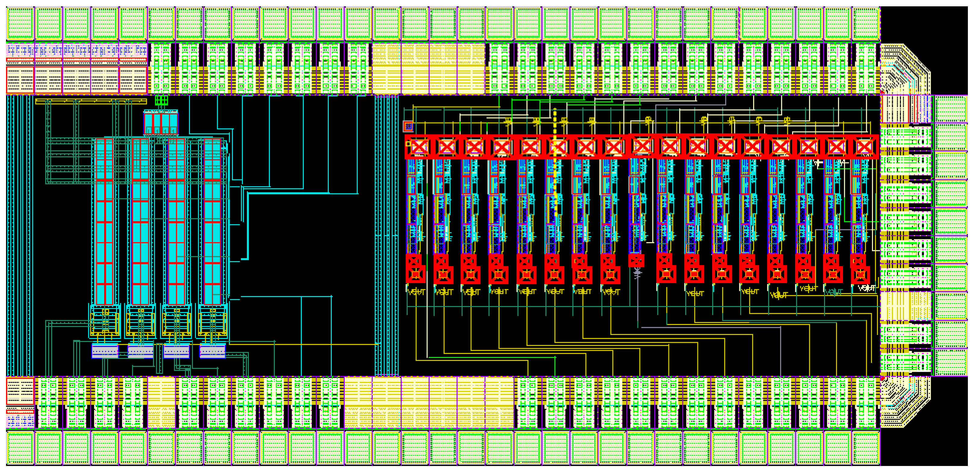
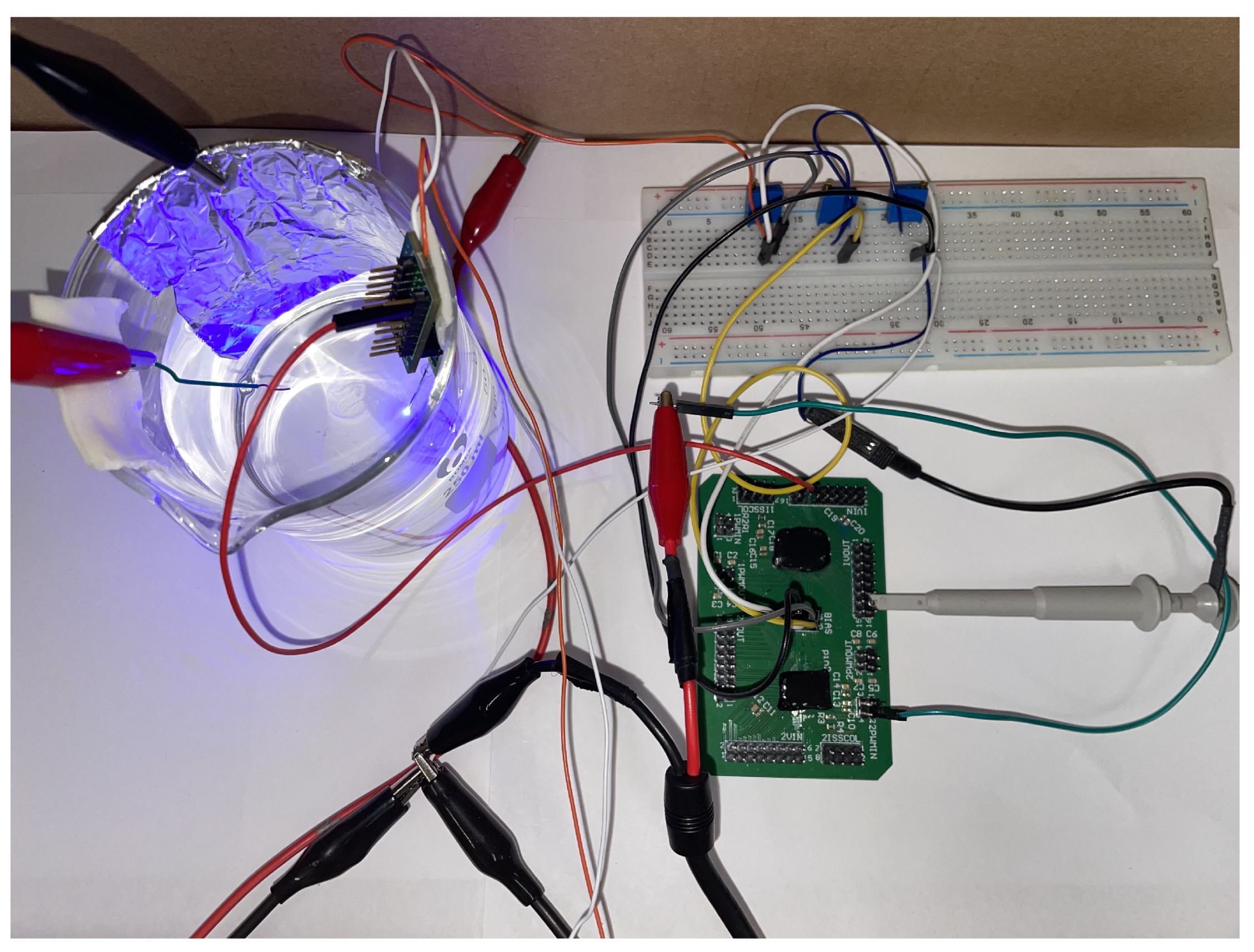
In order to address the drawbacks of previous works, this paper proposes a miniaturized and comprehensive optogenetic neuromodulation system composed of integrated circuits and a customized optrode. This ASIC consists of a 4-channel micro-LED driver module for driving micro-LEDs to stimulate neural cells, a 16-channel neural signal recording module for recording neural signals, and a micro-LED detection module for detecting the micro-LED’s working state in real time. The micro-LED driver model can adjust the driving current for the micro-LED, thus adjusting the luminosity of the light of the micro-LED. The micro-LED detection module could detect the micro-LED’s working state in real time without interfering with the neurostimulator circuits, and direct readout of the detection results, thereby avoiding subsequent complex data analysis of detection results.
This paper is arranged as the following structure. Section 2 presents the components of the optogenetic neuromodulation system. 
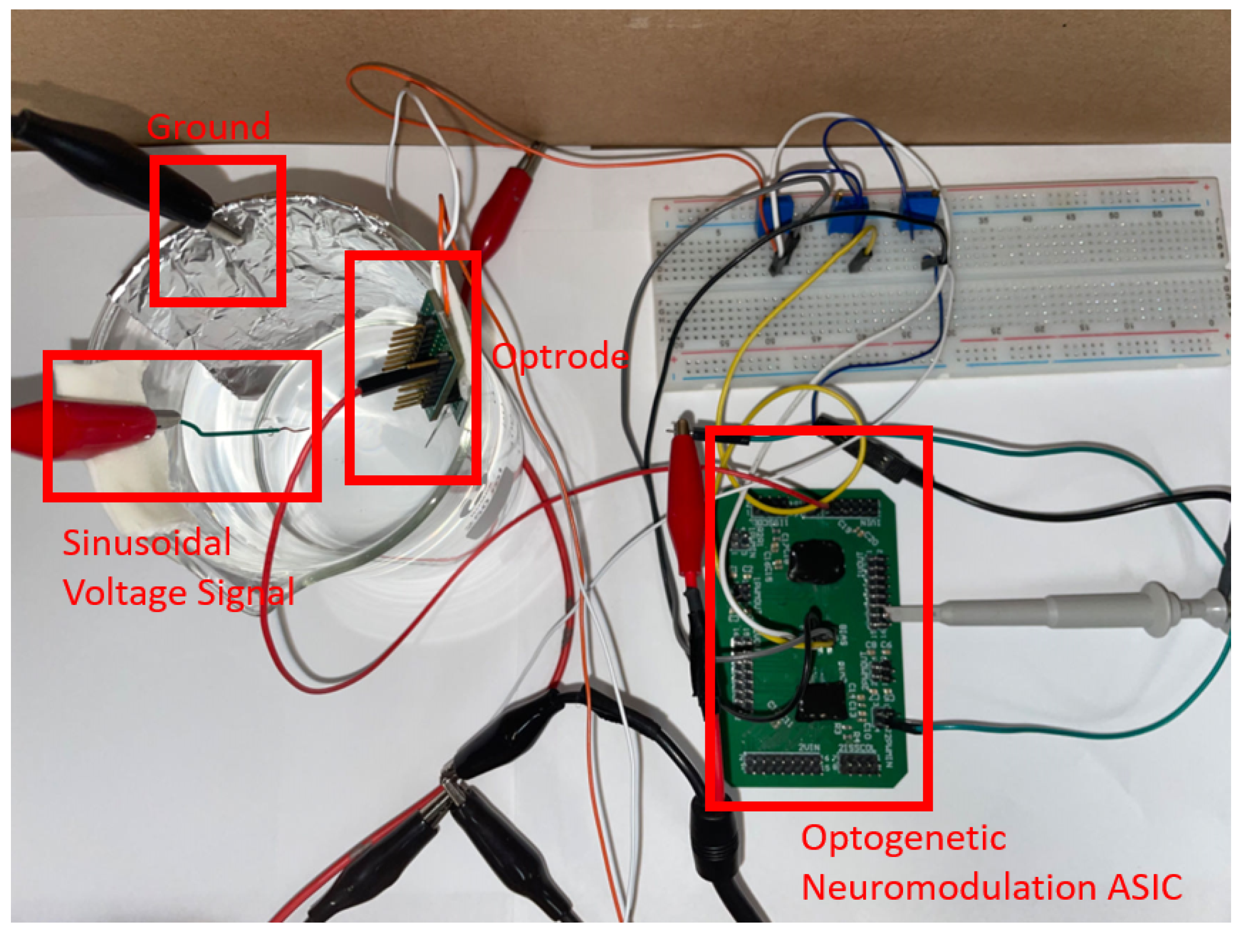
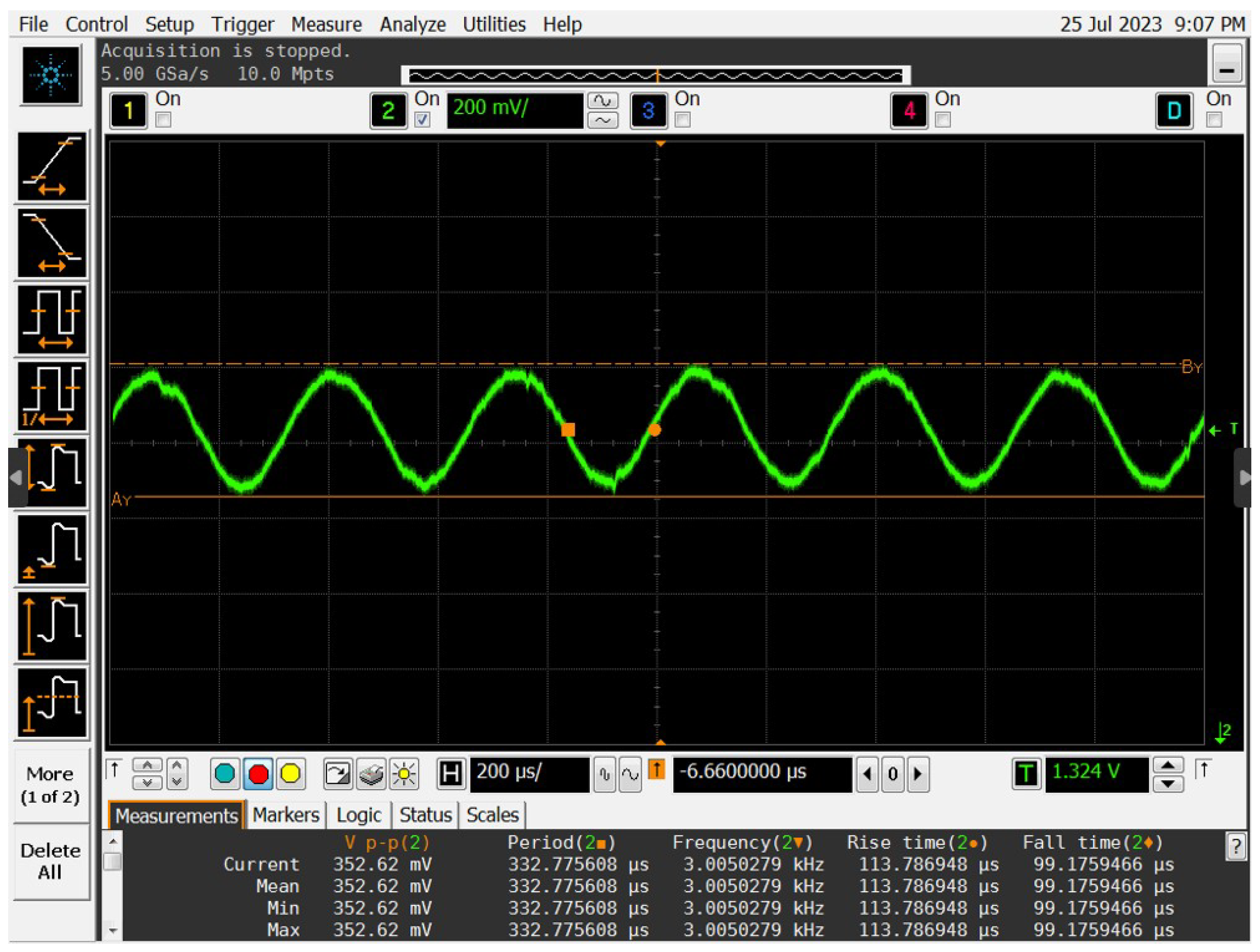
Section 3 presents the post-simulation results of the circuit system and the in situ normal saline experiment result. Section 4 discusses this work and summarizes the paper.

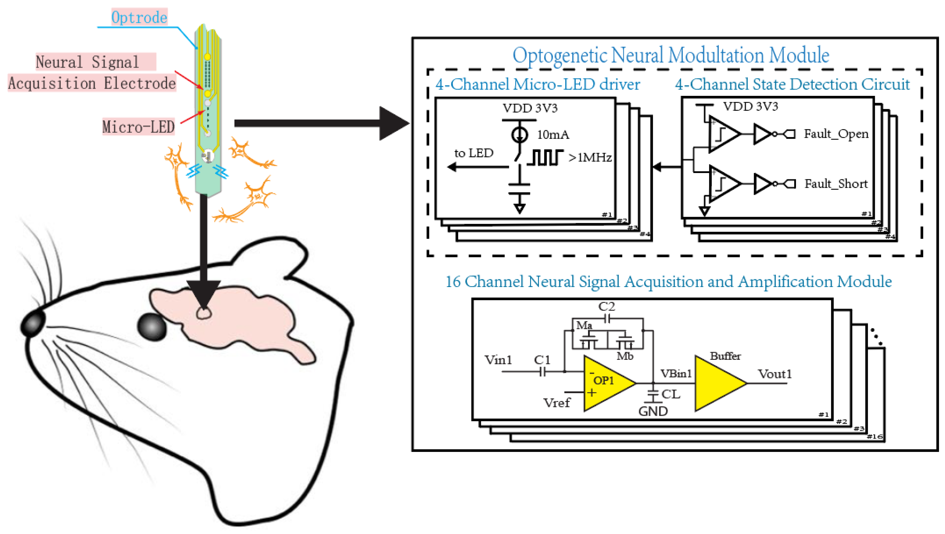
2. System Architecture

As shown in Figure 1, the top-level block of the presented optogenetic neuromodulator system consists of four modules: a customized optrode, a 4-channel micro-LED driver, a 4-channel micro-LED self-detection module, and a 16-channel neural signal recording module.
Two PWM control signals from external sources are utilized to adjust the working condition of the optogenetic stimulation circuit, where the low-frequency PWM (1–10 Hz) is for controlling the micro-LED driver circuit’s switching between the hibernation phase and the simulation phase, and the high-frequency PWM (1–10 MHz) is for adjusting the output current of the stimulation circuit during the stimulation phase.
The optrode may be broken during or after implantation, thus making the micro-LED not work accurately, so each optogenetic stimulation module is equipped with a consistently running self-detection module to evaluate the working state of the micro-LED. The user could justify three possible working states of micro-LED directly by the output voltage of two output nodes of the detection circuit.
The neuron activity could be monitored by the 16-channel neural signal recording circuit before, during, and after optogenetic stimulation. Monitoring neuron activity is not only useful for medical uses but can also help evaluate the optogenetic stimulation efficiency in real time; the user can adjust the optogenetic stimulation intensity to the minimum required level to reduce power consumption by the feedback of the neural signal recording circuit. An extra reference channel is equipped to reduce the interference of external noise.

2.1. Light Requirement and Optrode Characteristics

The light source used for stimulation needs to reach a certain threshold intensity to activate the simulated neurons. Simulation implies that the major contributor to the high energy demand for initiating an action potential is the restricted conductivity of ChR2 [16]. In 2003, Nagel et al. described that the activation threshold of cells that express ChR2 is 0.7 mW/mm2. However, different power intensity thresholds for stimulation have been published since then, and the most commonly used threshold is 1 mW/mm2, which can achieve strong neurostimulation.
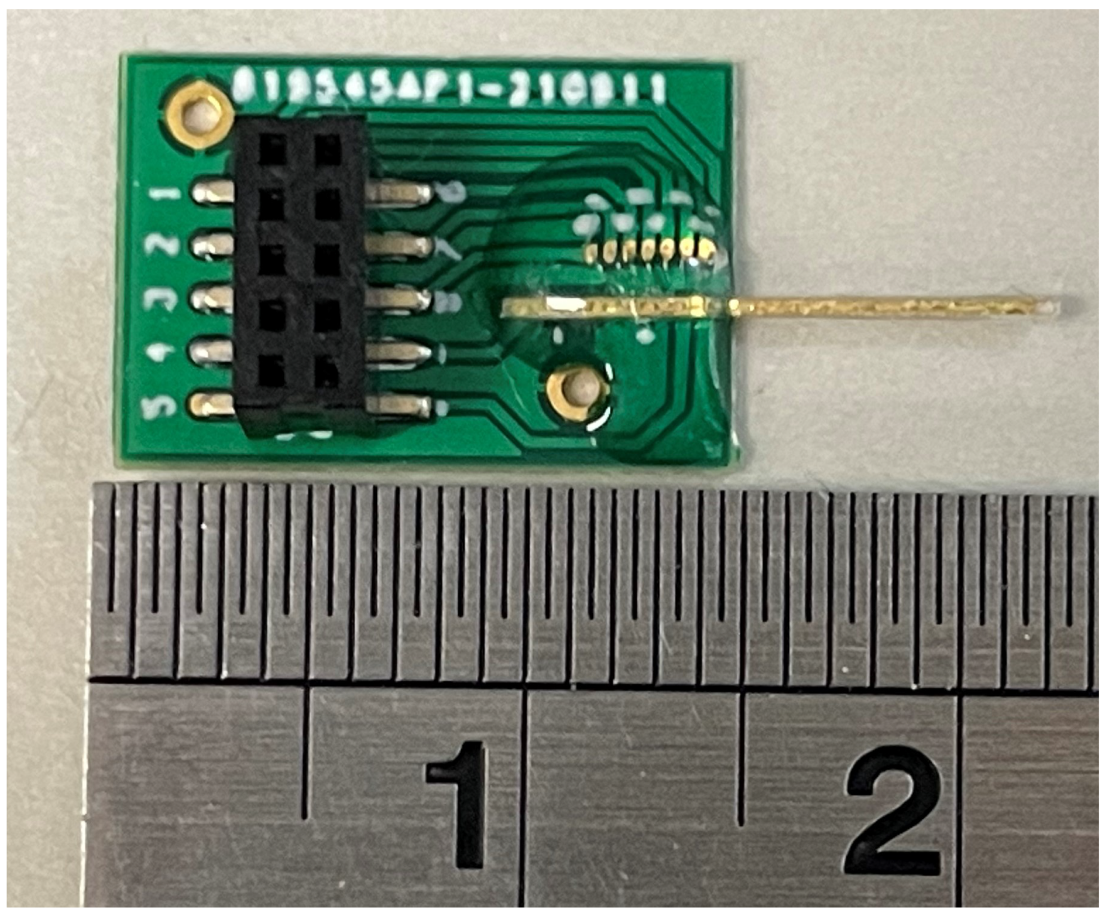
The customized planar optrode for the neuromodulation system was designed (see Figure 2), which was based on a sapphire substrate and processes the characteristics of high stiffness, high transparency, and high optogenetic density [17,18]. The optrode has a total length of L = 13 mm, with an 8 mm segment specifically reserved for the insertion into rodent brain tissue. The optrode comprised 4 GaN/InGaN multiple quantum-wells (MQWs) blue micro-LEDs serving as an excitation light source, along with 16 microelectrodes having a diameter of 10 µm. The optogenetic power density of a micro-LED is directly propotional to the driving current. At a current of 5 mA, the optogenetic power density can reach 1 mW/mm2 [17,18], which meets the threshold requirement for the strong optical neurostimulation mentioned earlier. These microelectrodes are comparable in size to the neurons.
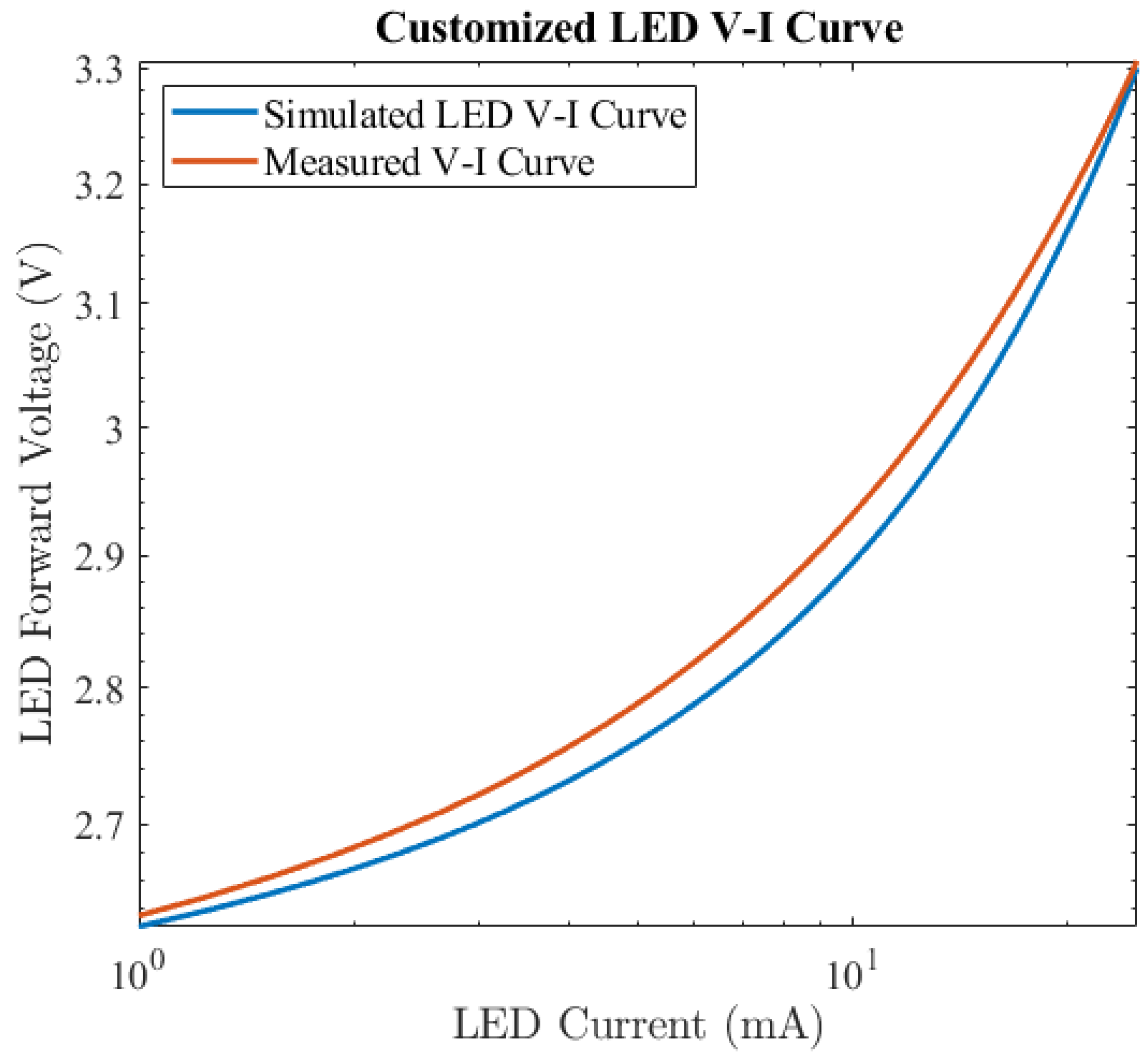
Based on the experiments, the micro-LED’s I-V curve was measured. According to the measured I-V curve, the micro-LED’s equivalent circuit was designed, which is used to replicate the characteristic I-V curve of the customized optrode, for the micro-LED driver circuit’s simulation. In the micro-LED equivalent circuit, an ideal comparator is utilized to create the turn-on voltage of the micro-LED, while the resistor Rs and a bipolar junction transistor are employed to generate an exponential relationship between the input voltage and the output current. The measured and simulated micro-LED I-V curves are presented in Figure 3.

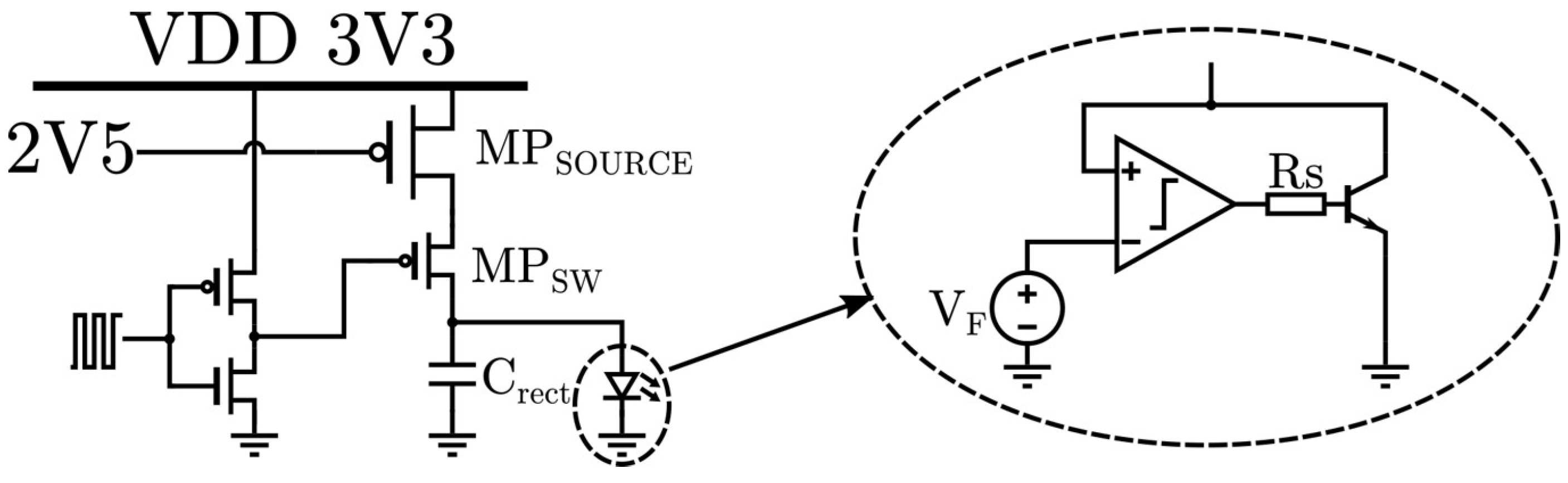
2.2. Micro-LED Driver Module

The micro-LED Driver Module is designed to provide a current output for driving micro-LEDs in an optrode for effective optogenetic stimulation. It has been observed that the luminance of a micro-LED has an explicit linear relationship to the current intensity [18], and the integral value of the irradiant density received by neurons within a short period of time will affect the response of neurons significantly [19,20]. Therefore, this variable-current-output Integrated Circuit (IC) is designed to precisely adjust the luminance of the micro-LED, thus enabling precise optogenetic neuromodulation stimulation. The structural diagram of this micro-LED driver circuit is presented in Figure 4.
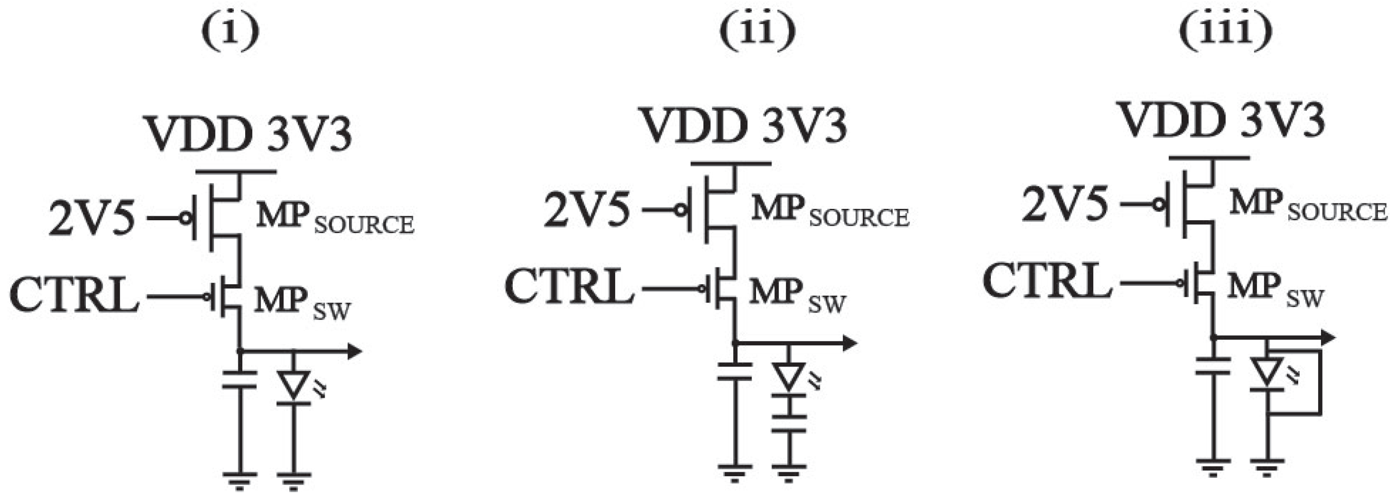
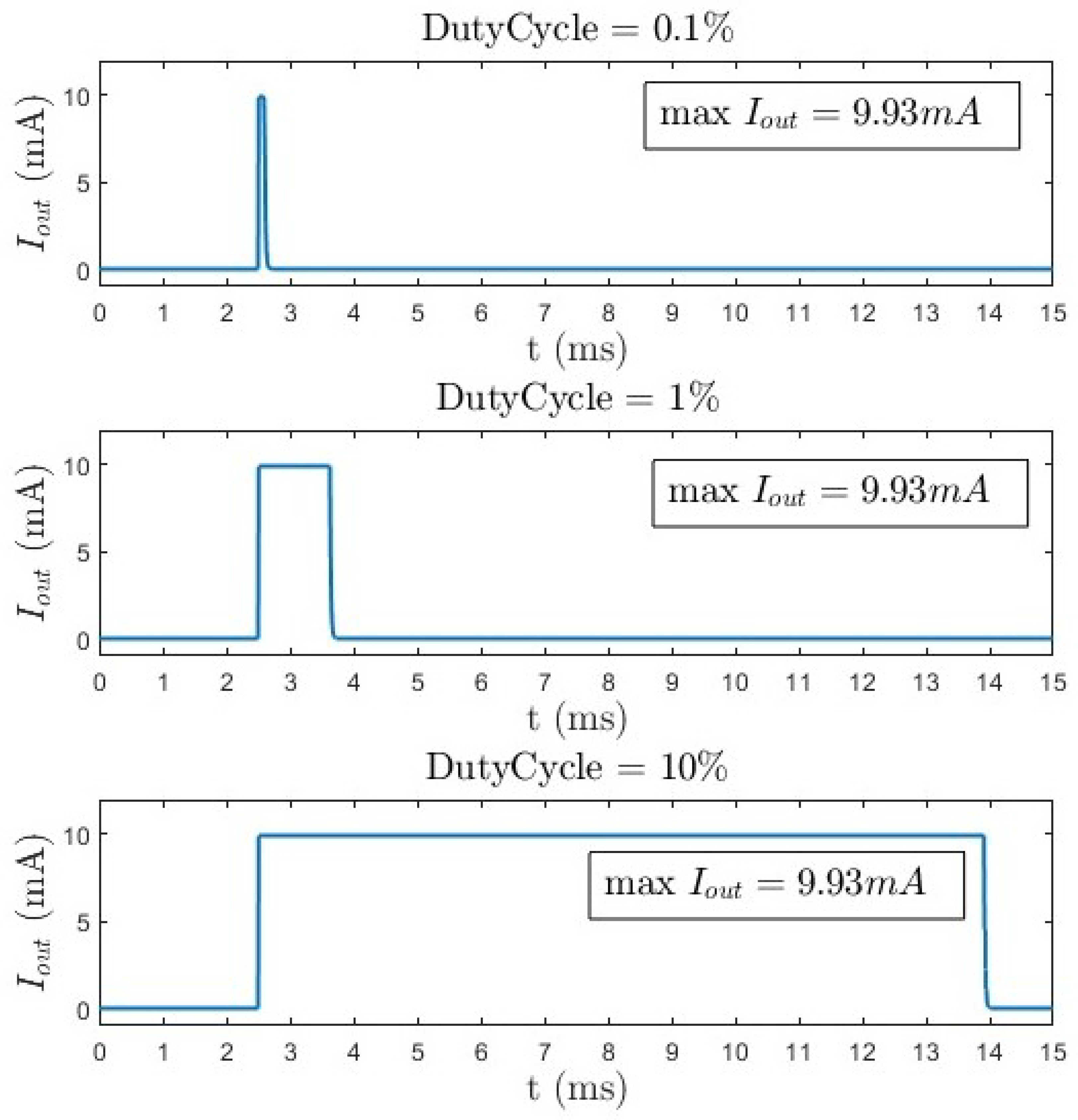
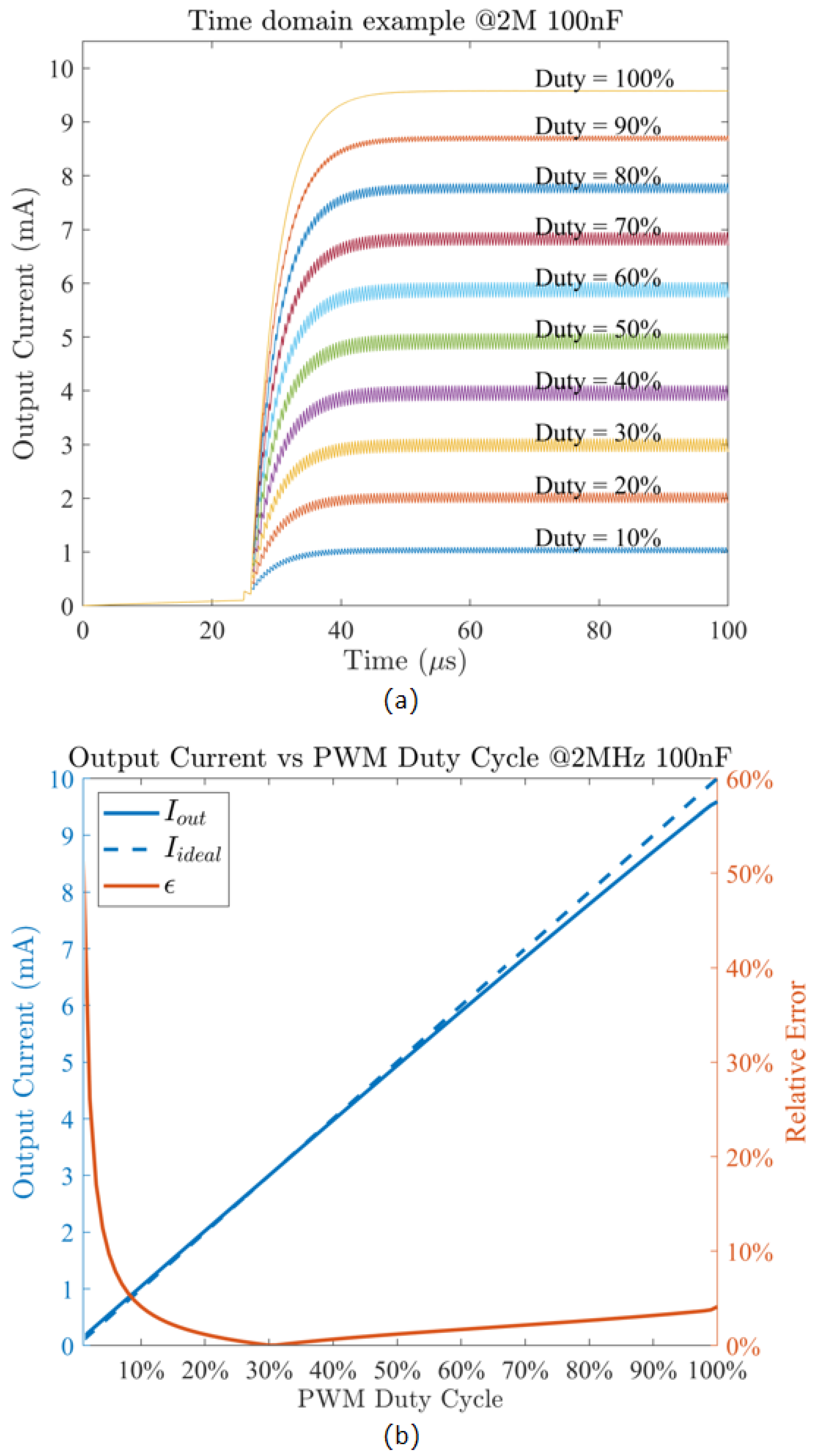
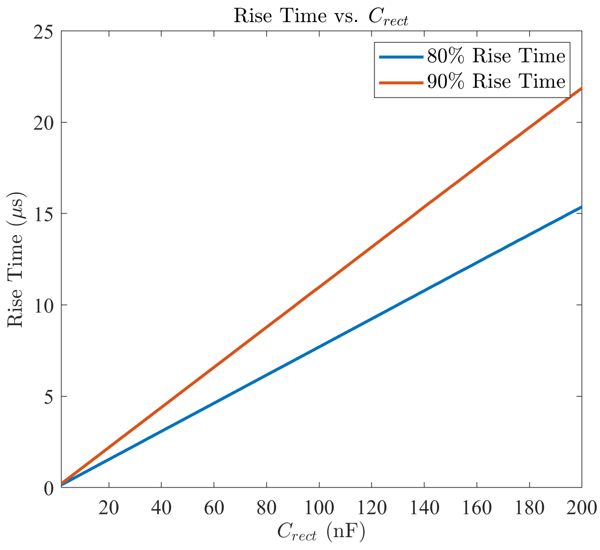
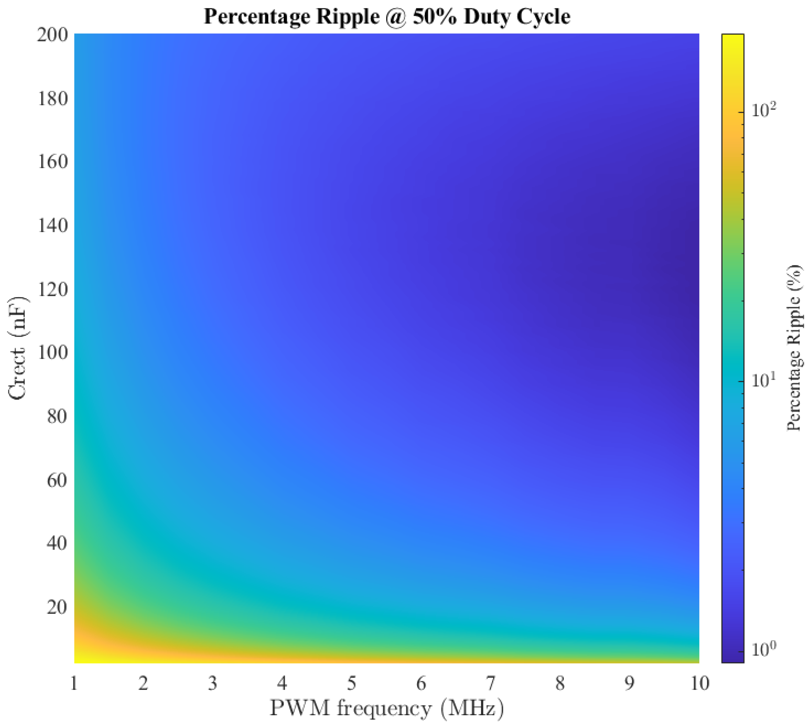
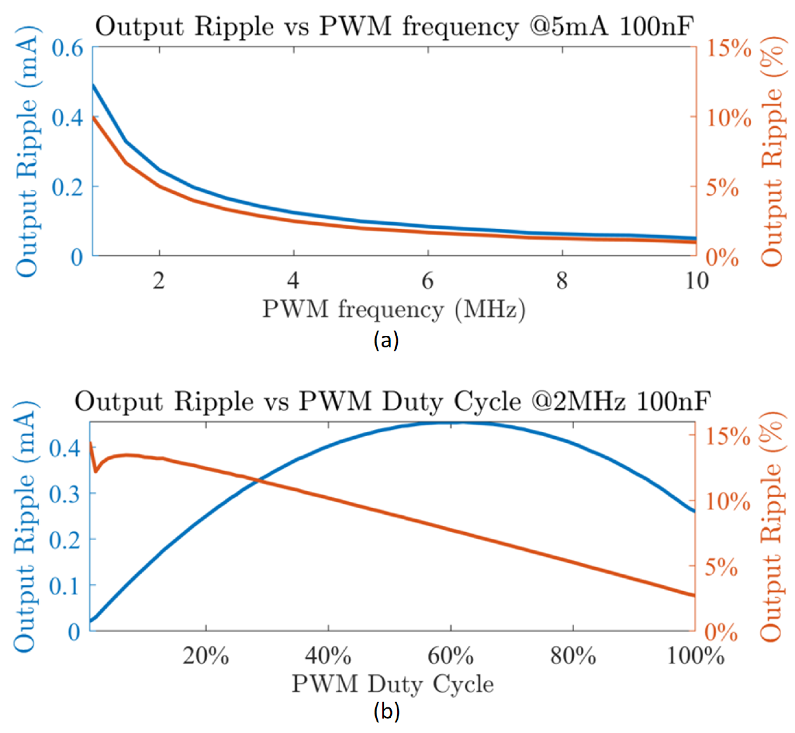
A pulse-width-modulation (PWM) controlled current mode output driver is used to drive the micro-LED in the optrode. MP SOURCE is biased by 2V5 voltage and works as a current source to supply a 10 mA current. Another MOSFET MP SW works as a switch, toggling the current source MOSFET on and off by the external control PWM signal to adjust the amplitude of the current flow into the micro-LED. The driving circuit adopts two kinds of PWM signal as the input control signal for adjusting the current duty cycle, magnitude, and frequency: the high-frequency PWM control signal is in the 1–10 MHz band, which is used to control the output current amplitude by adjusting the duty cycle of the PWM signal. The low-frequency PWM control signal is in the 1–10 Hz band, and it is used to control the duration of the stimulation time. The circuit uses an inverter for driving the switch MP sw to improve the switching speed. Since the optogenetic stimulation circuit is regulated by the PWM signal, the output current waveform inevitably has a ripple. In order to decrease the influence of the ripple, an off-chip filter capacitor C rect is equipped at the output node.

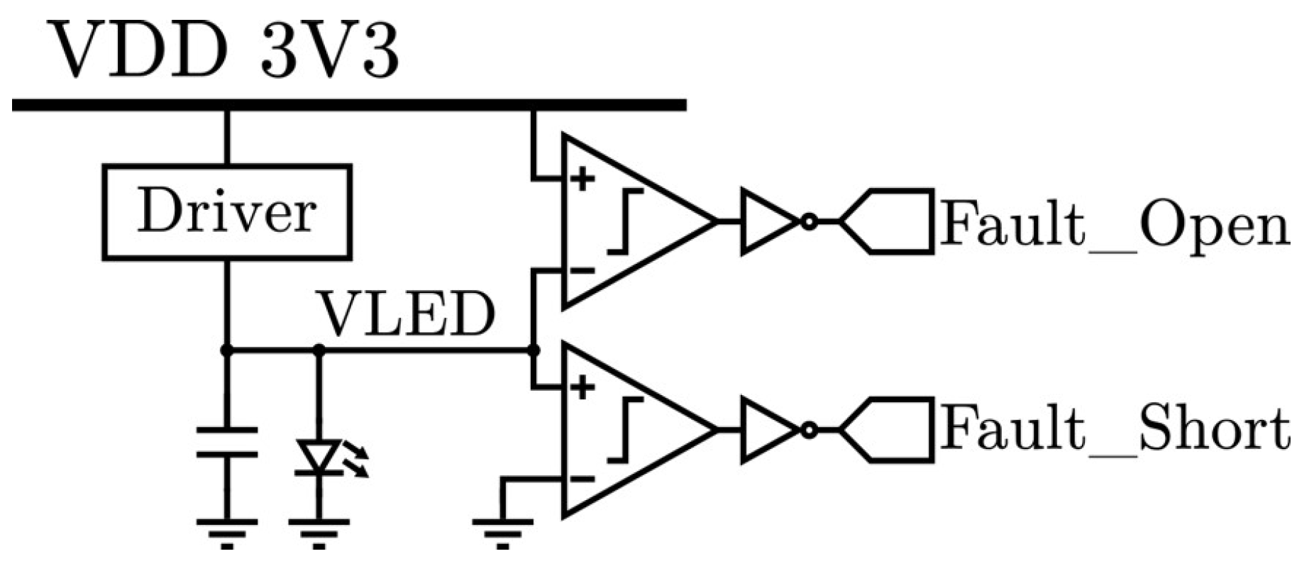
2.3. Micro-LED Self-Detection Module

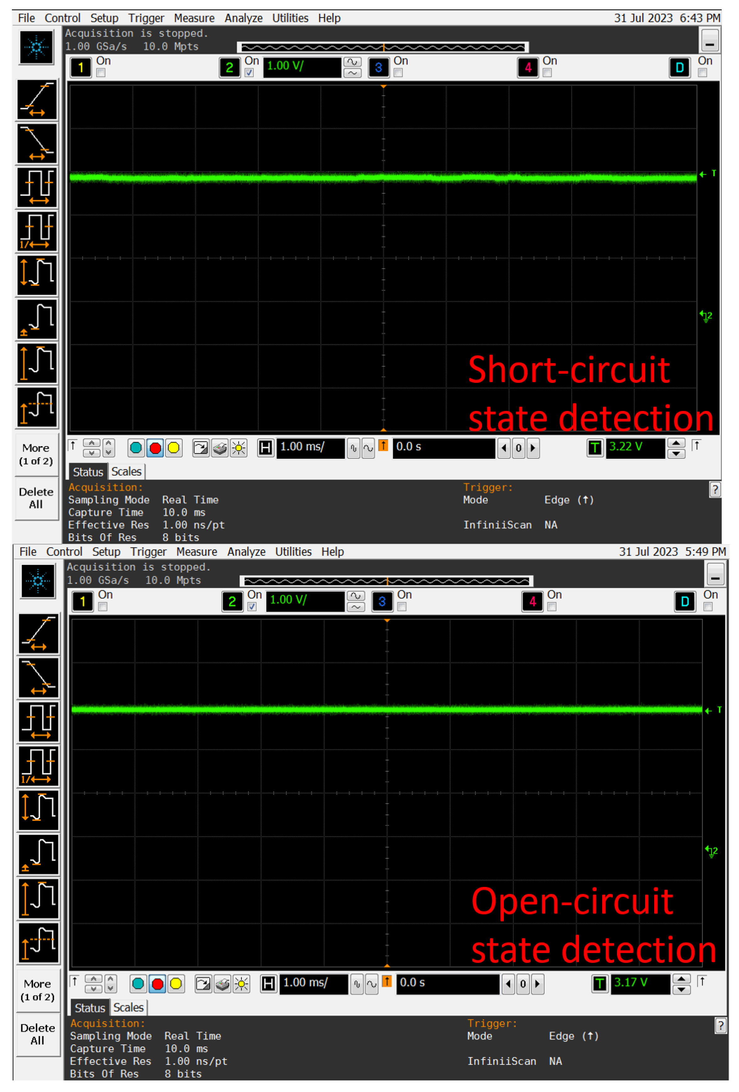
The micro-LED may be damaged during or after chronic implantation into the animal skull, which leads to an inability in the micro-LED to operate effectively and causes the luminance of the light to deviate from the predetermined value or the leakage current, which may affect neural signal recording and even damage brain tissue. Possible degradation mechanisms include open and short circuits of the micro-LED [14]. 
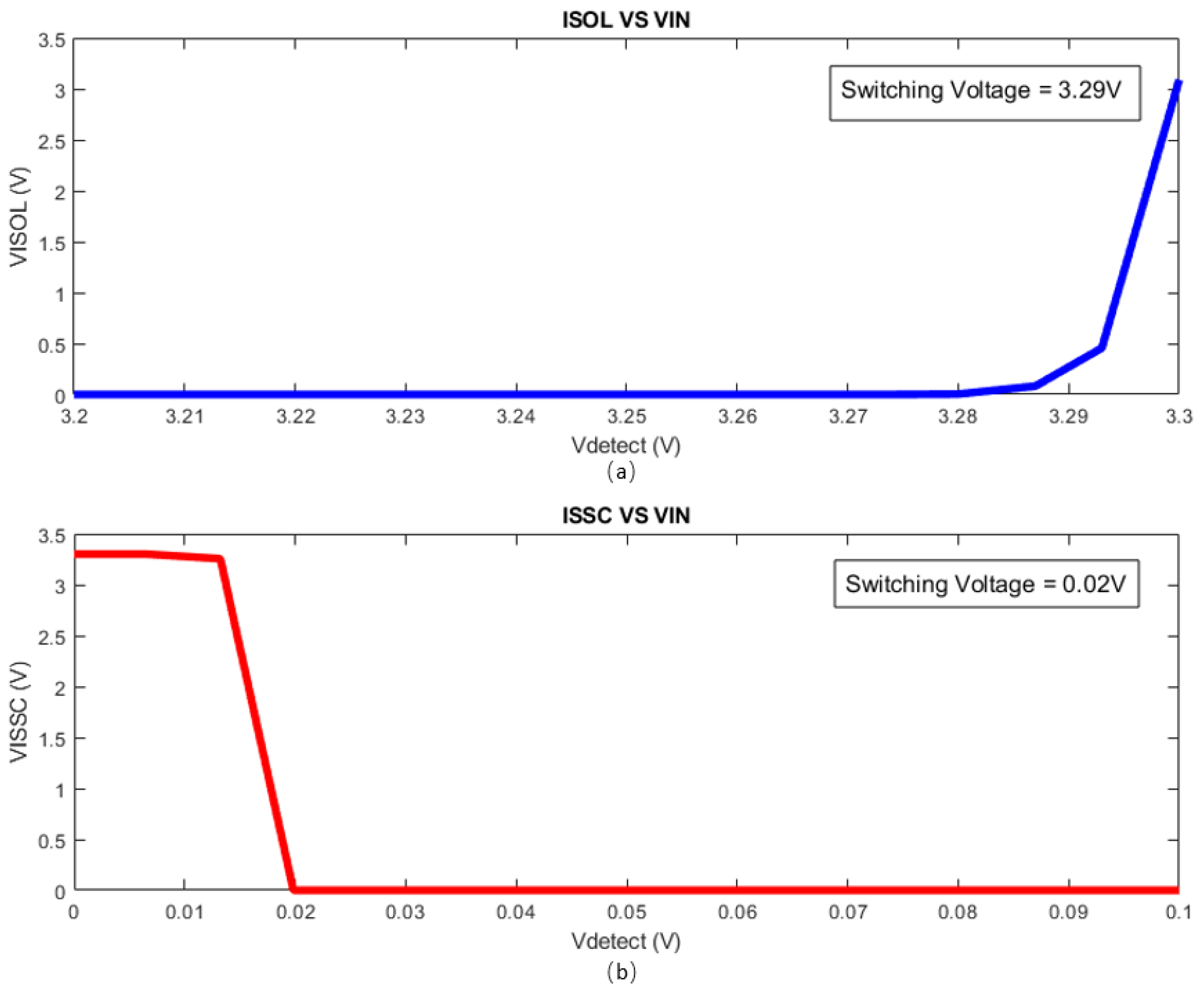
Figure 5 shows the circuit models under normal and two abnormal working states. The short circuit state can be represented by a short circuit between the micro-LED anode and cathode, and the open circuit state can be represented by a micro-LED cathode serial connection with a 10 pF capacitor. In the open circuit state, the drive current cannot flow out from the cathode of the micro-LED, so the anode voltage of the micro-LED is the power voltage VDD. In the short circuit state, the anode and cathode of the micro-LED are short-circuited; hence, the voltage of the anode is the ground voltage. Under the normal working state, the anode voltage of the micro-LED is between its turn-on voltage and power supply voltage. The self-detection module can judge the working state of the micro-LED by monitoring the anode voltage when the micro-LED is working, without interfering with the normal operation of the micro-LED.
The structure of the self-detection module is shown in Figure 6. The micro-LED anode voltage is compared with the power voltage and the ground voltage through two comparators, and the results are output at “SHORT” and “OPEN”. The output result of each output node is the power supply voltage (VDD) or ground voltage (GND), which, respectively, represents whether the micro-LED is in the OPEN state or SHORT. If the micro-LED operates normally, the output of both comparators is “0”. Specific possibilities and output results are shown in Table 1.

2.4. Neural Signal Recording Module

Neural signals generally have an amplitude of 10 µV to 100 µV [21], while the impedance of commonly used microelectrodes at 1 KHz is usually 100 K–100 MΩ. The electrochemical reaction between the microelectrode and the brain tissue will lead to several volts of DC offsets, which is much larger than the detected neural signal; thus, the capacitor-coupled input structure is used in the neural signal recording circuit to eliminate the DC offset. The neural signal spike has energy distribution within 100–7 KHz bandwidth [21], so the operational amplifier with a low cut-off frequency lower than 100 Hz and a high cut-off frequency higher than 10 KHz is required to acquire the neural signal.
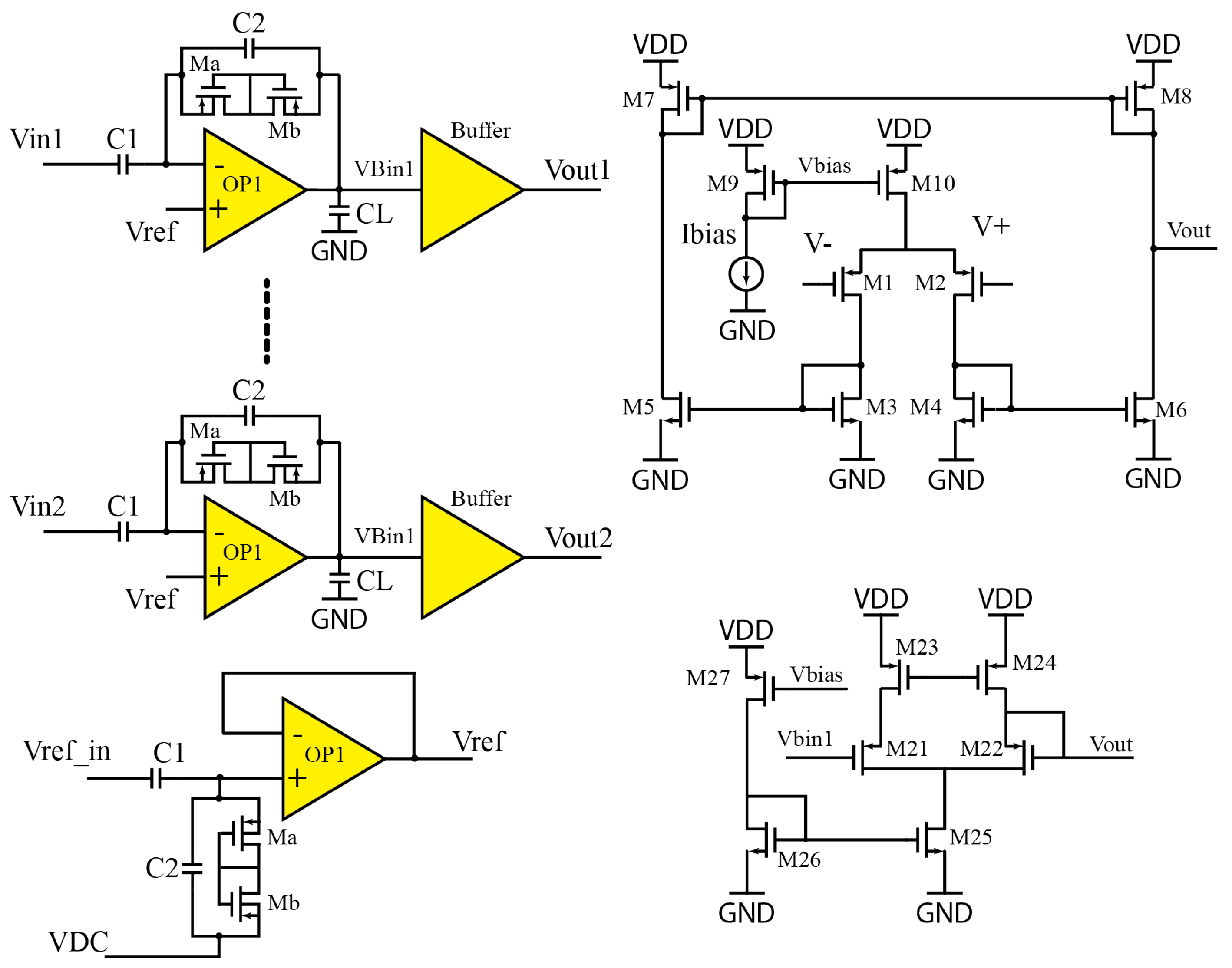
The 16-channel neural signal recording circuit is shown in 
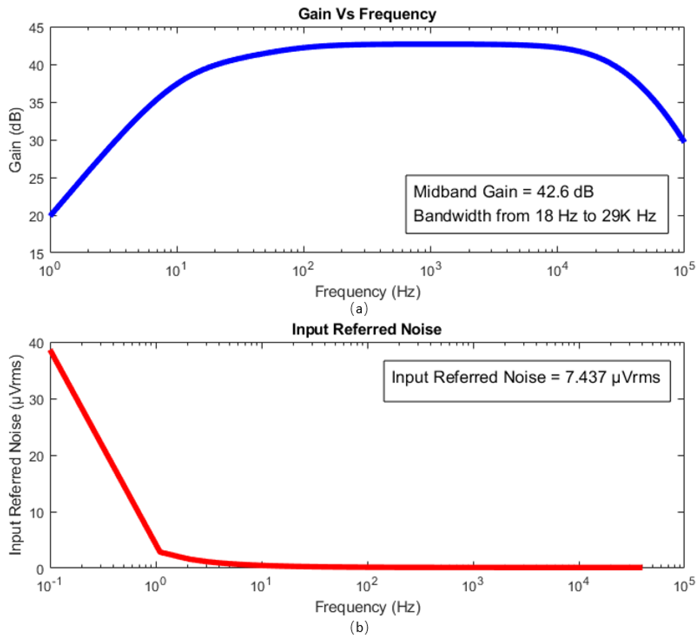
Figure 7. The front stage operational amplifier adopts a differential input to the single end output structure, the negative input terminal receives the neural signal sensed by the microelectrode, and the positive input terminal is connected to the reference channel’s output.
In order to decrease the low cutoff frequency of the amplifier to a very low level to acquire the neural signal as completely as possible, two MOSFETs are used to form a pseudo-resister device that has a very large resistance, and it is connected in parallel with the capacitor. The mid-band gain of the recorder circuit is C1/C2.
When the back-end stage is under heavy load (such as the probe of the oscilloscope), the quiescent point set by the circuit will shift, affecting the measurement results. In order to improve the driving capability of the circuit, the amplifier output is connected to a unity gain buffer stage, and the structure is also shown in Figure 7.
There is also a tradeoff between area, power, and noise performance in the design.
The structure of the operational amplifier in the reference channel is mostly the same as that of the operational amplifier in the recording channel, with the capacitor-coupled input to reduce DC offsets, and all the circuit components in the reference channel have the same parameters as the 16 neural signal recording channels to form the same bandwidth as the recording channel. The reference channel adopts the buffer connection method and is used to detect environmental noise. By using the reference channel, the environmental noise could be seen as the common-mode signal and be rejected by the differential input of the amplifier, thus improving the quality of the detected neural signal.
In addition, this design uses an advanced process (TSMC 65 nm) for fabricating, and the negative effect of gate-oxygen leakage cannot be ignored under the advanced process. Therefore, thick gate-oxygen MOSFET is used in this design to reduce gate-oxygen leakage and improve circuit performance.

3. Post-Simulation Results and Chip Post-Processing

3.1. Layout Design

Figure 8 shows the layout of the proposed optogenetic neuromodulation IC by the TSMC 65 nm process. The layout adopts a symmetrical design structure to decrease the influence of process error on the circuit performance. The layout adopts mimcap as the capacitor, which has higher accuracy but takes more area than momcap.
The signal lines bypass the capacitor to avoid coupling with the plate of the capacitor, which will affect the charge distribution of the capacitor. The PWM control signal lines of the micro-LED driver circuit are shielded by ground wires to reduce the interference between high-frequency control signals. Per-channel area of the neural signal acquisition and the amplifying module is 0.018 mm2, and the per-channel area of the micro-LED driver circuit with the self-detection circuit is 0.032 mm2.

3.2. Micro-LED Driver Circuit Simulation Result

Figure 9 shows the relationship between the output current of the micro-LED driver module and the low-frequency control signal. The input PWM low-frequency control signal is 10 Hz; the duty cycle is 0.1%, 1%, and 10%, respectively; the high-frequency control signal is 10 MHz with 100% duty cycle; and the output current is 9.93 mA, which is the maximum output current. From the plot, the duty cycle of the low-frequency PWM control signal controls the duration of the output current directly.
The output current of the micro-LED driver circuit with different high-frequency PWM control signal’s duty cycles is shown in Figure 10a, and it is proportional to the duty cycle of the high-frequency PWM control signal. The maximum current regulated by the circuit is approximately 10 mA with the 100% duty cycle high-frequency PWM control signal. However, due to the characteristics of a micro-LED, the output current has a certain pre-charge delay. Due to the existence of a filter capacitor, the output signal will have a rising edge.
Figure 10b presents the output current and high-frequency control signal’s relationship. The high-frequency PWM control signal used for the test is 2 MHz, and the duty cycle is changed from 0.1% to 100%. The test is conducted when the low-frequency PWM signal is high voltage. From the result, the output current is proportional to the high-frequency control signal’s duty cycle and could be regulated from 0.1 mA to nearly 10 mA. There are some errors between the ideal condition of the output current and the actual simulated output current. The output current is inaccurate at the minimum level, and the error is less than 5% in the working range of over 1 mA, which could be ignored.
The output ripple of the PWM circuit is inevitable because of the specific operating principle of the circuit; thus, a filter capacitor is needed to separate the DC component (proportional to the high-frequency PWM control signal’s duty cycle) from the unwanted AC ripple. The peak-to-peak ripple under the worst case (50% duty cycle of the high-frequency PWM control signal, T P W M is the PWM signal period, R is the equivalent output resistance) can be described in Equation (1):
V r i p p l e V f u l l s c a l e = T P W M 4 R C
The output signal’s settling time is shown in Equation (2):
T s e t t l e = R C · l n V f u l l s c a l e V r i p p l e
From the equations, selecting a large capacitor could help decrease the ripple but will increase the settling time, and a large capacitor will also increase the occupied area. Thus, there is a tradeoff between ripple magnitude, settling time, and taken area. Figure 11 shows the relationship between the rise time and the filter capacitor. The rise time increases as the capacitance of the filter capacitor increases, which validates Equation (1). The output ripple is analyzed during the design of the circuit. Figure 12 summarizes the relationship between the PWM frequency, filter capacitor, and the percentage ripple. Through the results from Figure 11 and Figure 12, 100 nf is selected as the capacitance of the filter capacitor for the tradeoff between rise time, percentage ripple, and taken area.
The relationship between the output ripple and PWM frequency and PWM duty cycle, respectively, is shown in Figure 13. The output ripple percentage decrease with the PWM frequency and the PWM duty cycle. The maximum amplitude of an output ripple current with a 5 mA output is 0.5 mA, which also accounts for the largest proportion of the output current (10%). At a given frequency (2 MHz), the magnitude of the ripple is the largest (0.5 mA) when the PWM signal is at 60% duty cycle, and the ratio of the output ripple to the output current is also maximized (15%).

3.3. Micro-LED Detection Circuit Simulation Result

The open-loop detection and short-circuit detection results are shown in Figure 14a and Figure 14b, respectively. When the detected voltage is close to ground voltage, the short circuit module’s output voltage is “0” (close to GND), proving that micro-LED works in the short-circuit state. When the detected voltage is close to VDD, the micro-LED works in an open-loop state, and the output voltage of the open-loop node is closed to VDD. The switching voltage for the short-circuit detection and open-loop detection is 0.02 V and 3.29 V, respectively.

3.4. Neural Signal Recording Circuit Simulation Result

A series of simulations for the 16-channel neural signal recording circuit is conducted to determine its electrical performance. Figure 15a shows the relationship between the gain and frequency. The amplifier mid-band gain is 42.6 dB, and the −3 dB bandwidth is from 18 Hz to 29 kHz. The 42.6 dB amplifier gain suffices the requirement.
Figure 15b shows the input-referred noise performance of the circuit. The action potential is mainly distributed in the 100 Hz–7 KHz [17] frequency range, and the input integral noise within this bandwidth is 7.437 µVrms. The equivalent input-referred noise is mainly contributed by two input transistors, and this noise level could meet the requirement of a minimum SNR of 2 for a 50 µV neural signal. The power consumption of one channel is 12 µW, and the low power consumption of the circuit maximizes the protection of the brain tissue around the chip after implantation from the thermal of the chip. Each channel takes 0.018 mm2 in area. There is a tradeoff between noise performance, area, and power consumption. The circuit achieves a small area and low power consumption by sacrificing the noise performance of the circuit. Each channel improves the driving ability through the subsequent buffer, and it can drive a 1 nF capacitor.

3.5. In Situ Normal Saline Experiment Result

To verify the function of the neuromodulation system, an in situ experiment was conducted. The experiment was carried out within a faradic cage to maintain an electromagnetically shielded environment for evaluating the neuromodulation system’s functionality. The optrode was immersed in the normal saline environment, which is used to mimic the interstitial fluid environment, and a sinusoidal voltage signal (1 KHz, 200 mV) from the function generator was introduced into the saline solution to simulate the neural signal evoked by the optogenetic stimulation. The experiment environment is shown in Figure 16.
A 10M Hz PWM signal with a 50% duty cycle was produced from the function generator as the control signal for the optogenetic stimulation module, then the micro-LED was illuminated, emitting blue light (Figure 17). Simultaneously, a sinusoidal voltage signal was introduced into the saline, sensed, and amplified by the recording module (Figure 18). From the result, the signal wave was amplified nearly 180 times by the recording module.
To test the optrode detection module, two additional control scenarios were employed: firstly, the optrode was disconnected with the chip to simulate the micro-LED open-circuit state, and secondly, the anode of the micro-LED and the ground of the neuromodulation system were connected to simulate the micro-LED short-circuit state. From the result (Figure 19), the detection module’s two outputs will be “1” (nearly the VDD voltage) individually when these two unexpected conditions happen.

4. Discussion and Conclusions

The optogenetic neuromodulation technique is important in the field of brain science because of its spatially confined stimulation and neuron-type specificity. However, existing optogenetic neuromodulation systems still face the challenges of bulky physical size, incomplete system functionality, and non-direct output detection result. To this end, this paper proposed an optogenetic neuromodulation ASIC with the component modules of a 4-channel micro-LED driver, a 4-channel micro-LED self-detection module, and a 16-channel neural signal recording module. The comparison between this work and the previous works is shown in Table 2. Compared with previous work, this ASIC is fully featured and a miniaturization, the detection circuit can monitor the micro-LED in real time without interfering with other circuit modules, and users can know the working status of the micro-LED without post-analysis. Due to the PWM driving circuit’s inherent operating principle, the output ripple is inevitable. Although adding the filter capacitor could help reduce the output ripple, it will increase the settling time and the taken area. The ASIC was fabricated by the TSMC 65 nm process, and an in situ normal saline experiment was conducted to test the neuromodulation system’s function. In vitro and in vivo experiments are future works.

Author Contributions

Conceptualization, Y.X. (Yu Xia), L.W. and S.H.P.; methodology, Y.X. (Yu Xia), R.Z., L.W. and S.H.P.; software, Y.X. (Yu Xia), R.Z., D.L. and L.W.; validation, Y.X. (Yu Xia), L.W. and Y.X. (Yanyan Xu); formal analysis, Y.X. (Yu Xia) and L.W.; investigation, Y.X. (Yu Xia); resources, B.Z., P.U.M., M.I.V. and S.H.P.; writing—original draft preparation, Y.X. (Yu Xia); writing—review and editing, L.W., A.Z., Y.W. and S.H.P.; supervision, S.H.P.; project administration, M.I.V. and S.H.P.; funding acquisition, Y.G., H.L., P.U.M., M.I.V. and S.H.P. All authors have read and agreed to the published version of the manuscript.

Funding

This work was funded by the joint funding of the Nature Science Foundation of China (NSFC) and the Macao Science and Technology Development Fund (FDCT) of China (Grant No. 62061160368); the National Key Research and Development Program of China (No. 2020YFB1313502, No. 2021ZD0201300); the Blue Ocean Smart System (Nanjing) Limited (CP-003-2023); the Shenzhen-Hong Kong-Macau S&T Program (Category C) of SZSTI (SGDX20201103094002009); the University of Macau (File no. MYRG2020-00098-FST, MYRG2022-00111-IME); the Science and Technology Development Fund, Macau SAR (File no. 0144/2019/A3, 0022/2020/AFJ, SKL-AMSV(UM)-2023-2025); the ZUMRI-Lingyange Semiconductor Joint Lab (CP-031-2022); the Lingyange Semiconductor Incorporated, Zhuhai (CP-017-2022); the National Natural Science Foundation of China, grant number 62371136; the Project of Chinese Ministry of Science and Technology, grant number 2022YFE0115500; and the Project of S&T Department of Fujian Province, grant number 2021I0005.

Institutional Review Board Statement

Not applicable.

Informed Consent Statement

Not applicable.

Data Availability Statement

All data underlying the results are available as part of the article and no additional source data are required.

Acknowledgments

The authors would also like to acknowledge the financial support of Lingyange Semiconductor Incorporated, ZHUHAI, and the Blue Ocean Smart System (NANJING).

Conflicts of Interest

The authors declare no conflict of interest.

References

  1. Jiang, S.; Wu, X.; Rommelfanger, N.J.; Ou, Z.; Hong, G. Shedding light on neurons: Optical approaches for neuromodulation. Natl. Sci. Rev. 2022, 9, nwac007. [Google Scholar] [CrossRef] [PubMed]
  2. Aronowitz, F. Theory of a Traveling-Wave Optical Maser. Phys. Rev. 1965, 139, A635–A646. [Google Scholar] [CrossRef]
  3. Gaily, T.D. Optical Absorption Coefficient of Molecular Oxygen near 1215 Angstroms. J. Opt. Soc. Am. 1969, 59, 536–538. [Google Scholar] [CrossRef]
  4. Wang, L.; Wu, X.; Yang, G.; Hu, N.; Zhao, Z.; Zhao, L.; Li, S. Cannabidiol Alleviates the Damage to Dopaminergic Neurons in 1-Methyl-4-Phenyl-1,2,3,6-Tetrahydropyridine-Induced Parkinson’s Disease Mice via Regulating Neuronal Apoptosis and Neuroinflammation. Neuroscience 2022, 498, 64–72. [Google Scholar] [CrossRef] [PubMed]
  5. Hochberg, L.R.; Serruya, M.D.; Friehs, G.M.; Mukand, J.A.; Saleh, M.; Caplan, A.H.; Branner, A.; Chen, D.; Penn, R.D.; Donoghue, J.P. Neuronal ensemble control of prosthetic devices by a human with tetraplegia. Nature 2006, 442, 164–171. [Google Scholar] [CrossRef] [PubMed]
  6. Collinger, J.L.; Wodlinger, B.; Downey, J.E.; Wang, W.; Tyler-Kabara, E.C.; Weber, D.J.; McMorland, A.J.; Velliste, M.; Boninger, M.L.; Schwartz, A.B. High-performance neuroprosthetic control by an individual with tetraplegia. Lancet 2013, 381, 557–564. [Google Scholar] [CrossRef] [PubMed]
  7. Zanos, S. Closed-loop neuromodulation in physiological and translational research. Cold Spring Harb. Perspect. Med. 2019, 9, a034314. [Google Scholar] [CrossRef] [PubMed]
  8. Vidal, J.; Ghovanloo, M. Towards a switched-capacitor based stimulator for efficient deep-brain stimulation. In Proceedings of the 2010 Annual International Conference of the IEEE Engineering in Medicine and Biology, Buenos Aires, Argentina, 31 August–4 September 2010; pp. 2927–2930. [Google Scholar]
  9. Marzouk, A.M.; Stanitzki, A.; Kokozinski, R. Towards pulse-density modulated functional electrical stimulation of neural cells with passive membranes. In Proceedings of the PRIME 2012, 8th Conference on Ph.D. Research in Microelectronics & Electronics, Aachen, Germany, 12–15 June 2012; pp. 1–4. [Google Scholar]
  10. Haas, M.; Vogelmann, P.; Ortmanns, M. A Neuromodulator Frontend With Reconfigurable Class-B Current and Voltage Controlled Stimulator. IEEE Solid-State Circuits Lett. 2018, 1, 54–57. [Google Scholar] [CrossRef]
  11. Reich, S.; Sporer, M.; Haas, M.; Becker, J.; Schüttler, M.; Ortmanns, M. A High-Voltage Compliance, 32-Channel Digitally Interfaced Neuromodulation System on Chip. IEEE J. Solid-State Circuits 2021, 56, 2476–2487. [Google Scholar] [CrossRef]
  12. Eberhard, D.; Voges, E. Digital single sideband detection for interferometric sensors. In Proceedings of the 2nd Intl Conf on Optical Fiber Sensors: OFS’84, Stuttgart, Germany, 5–7 September 1984; Volume 514, pp. 381–386. [Google Scholar]
  13. Cao, H.; Gu, L.; Mohanty, S.; Chiao, J.C. An integrated μLED optrode for optogenetic stimulation and electrical recording. IEEE Trans. Biomed. Eng. 2012, 60, 225–229. [Google Scholar] [CrossRef] [PubMed]
  14. Zhao, H.; Soltan, A.; Maaskant, P.; Dong, N.; Sun, X.; Degenaar, P. A scalable optoelectronic neural probe architecture with self-diagnostic capability. IEEE Trans. Circuits Syst. I Regul. Pap. 2018, 65, 2431–2442. [Google Scholar] [CrossRef]
  15. Mendrela, A.E.; Kim, K.; English, D.; McKenzie, S.; Seymour, J.P.; Buzsáki, G.; Yoon, E. A High-Resolution Opto-Electrophysiology System with a Miniature Integrated Headstage. IEEE Trans. Biomed. Circuits Syst. 2018, 12, 1065–1075. [Google Scholar] [CrossRef] [PubMed]
  16. Foutz, T.J.; Arlow, R.L.; McIntyre, C.C. Theoretical principles underlying optical stimulation of a channelrhodopsin-2 positive pyramidal neuron. J. Neurophysiol. 2012, 107, 3235–3245. [Google Scholar] [CrossRef] [PubMed]
  17. Shen, J.; Xu, Y.; Xiao, Z.; Liu, Y.; Liu, H.; Wang, F.; Yan, C.; Wang, L.; Chen, C.; Wu, Z.; et al. Double-Sided Sapphire Optrodes with Conductive Shielding Layers to Reduce Optogenetic Stimulation Artifacts. Micromachines 2022, 13, 1836. [Google Scholar] [CrossRef] [PubMed]
  18. Shen, J.; Xu, Y.; Xiao, Z.; Liu, Y.; Liu, H.; Wang, F.; Yao, W.; Yan, Z.; Zhang, M.; Wu, Z.; et al. Influence of the Surface Material and Illumination upon the Performance of a Microelectrode/Electrolyte Interface in Optogenetics. Micromachines 2021, 12, 1061. [Google Scholar] [CrossRef]
  19. Grossman, N.; Nikolic, K.; Toumazou, C.; Degenaar, P. Modeling study of the light stimulation of a neuron cell with channelrhodopsin-2 mutants. IEEE Trans. Biomed. Eng. 2011, 58, 1742–1751. [Google Scholar] [CrossRef] [PubMed]
  20. Nikolic, K.; Grossman, N.; Grubb, M.S.; Burrone, J.; Toumazou, C.; Degenaar, P. Photocycles of channelrhodopsin-2. Photochem. Photobiol. 2009, 85, 400–411. [Google Scholar] [CrossRef] [PubMed]
  21. Harrison, R.R.; Charles, C. A low-power low-noise CMOS amplifier for neural recording applications. IEEE J.-Solid-State Circuits 2003, 38, 958–965. [Google Scholar] [CrossRef]
Figure 1. Block diagram of the proposed multi-function optogenetic neuromodulation system.
Electronics 12 04783 g001
Figure 2. Customized optrode.
Electronics 12 04783 g002
Figure 3. Simulated and measured micro-LED I-V curve.
Electronics 12 04783 g003
Figure 4. Schematic of the micro-LED driving circuit and micro-LED equivalent circuit.
Electronics 12 04783 g004
Figure 5. Equivalent circuit models of micro-LED’s 3 working states. (i) Normal working state. (ii) Open-loop working state. (iii) Short-circuit working state.
Electronics 12 04783 g005
Figure 6. Schematic of the uLED detection module.
Electronics 12 04783 g006
Figure 7. Schematic of the 16-channel neural signal acquisition and amplification module.
Electronics 12 04783 g007
Figure 8. Layout of the proposed ASIC.
Electronics 12 04783 g008
Figure 9. Simulation results of the relationship between the output duration and low-frequency PWM signal’s duty cycle.
Electronics 12 04783 g009
Figure 10. (a) Relationship between output current magnititude and high-frequency PWM control signal’s duty cycle, (b) output current vs. high-frequency PWM signal’s duty cycle.
Electronics 12 04783 g010
Figure 11. Relationship between filter capacitor and rise time.
Electronics 12 04783 g011
Figure 12. Relationship between output current magnititude and high-frequency PWM control signal’s duty cycle.
Electronics 12 04783 g012
Figure 13. (a) Relationship between output ripple and PWM frequency, (b) relationship between output ripple and PWM duty cycle.
Electronics 12 04783 g013
Figure 14. (a) The open-loop detection result, (b) the short-circuit detection result.
Electronics 12 04783 g014
Figure 15. (a) Relationship between output ripple and PWM frequency, (b) relationship between output ripple and PWM duty cycle.
Electronics 12 04783 g015
Figure 16. The in situ normal saline experiment environment.
Electronics 12 04783 g016
Figure 17. The PWM is turned on after inputting a PWM control signal.
Electronics 12 04783 g017
Figure 18. The recording module sensed the signal and amplified it 180 times.
Electronics 12 04783 g018
Figure 19. The optrode detection module experiment result. Two nodes of the detection module output digital voltage “1” in open-circuit and short-circuit states, respectively.
Electronics 12 04783 g019
Table 1. Specific possibilities and output results of the micro-LED detection module.
Fault_OpenFault_ShortMicro-LED Working State
lowlowNormal
highlowOpen Loop
lowhighShort Circuit
highhighImpossible
Table 2. Comparison with Other Neuromodulation Asics.
TCAS-I [13]TBME [18]TBME [19]TBIOCAS [20]TBIOCAS [21]This Work
Year20182017202120182018This Work
Process0.35-µm0.18-µm65-nm0.35-µm0.18-µm65-nm
Recording IC ChannelsNO4NO4NO16
Power of recording channelsNO1.65 mWNO11.8 µWNO11.76 µW
Per recording channel’s areaNONANONONA0.018 mm2
Stimulation methodoptogeneticoptogeneticoptogeneticoptogeneticoptogeneticoptogenetic
Stimulation IC channels188326124
Per stimulation channel’sNANA0.025 mm2NA0.272 mm20.032 mm2
Maximum stimulation current4.37 mANA0.9 mA1.1 mA10 mA10 mA
Micro-LED detection functionYES (non-real-time)NONONONOYES (real-time)
Disclaimer/Publisher’s Note: The statements, opinions and data contained in all publications are solely those of the individual author(s) and contributor(s) and not of MDPI and/or the editor(s). MDPI and/or the editor(s) disclaim responsibility for any injury to people or property resulting from any ideas, methods, instructions or products referred to in the content.

