
Design and Analysis of a Novel High-Gain DC-DC Boost Converter with Low Component Count

1
Faculty of Engineering, University of Central Punjab, Lahore 42000, Pakistan
2
Department of Electrical Engineering, Ghulam Ishaq Khan University, Topi 23640, Pakistan
3
Politecnico di Torino, Department of Electronics and Telecommunication (DET), Polytechnic University of Turin, 10129 Turin, Italy
*
Author to whom correspondence should be addressed.
Electronics 2021, 10(15), 1761; https://doi.org/10.3390/electronics10151761
Submission received: 8 June 2021
/
Revised: 16 July 2021
/
Accepted: 21 July 2021
/
Published: 23 July 2021
(This article belongs to the Section Power Electronics)
Abstract
:In this paper, a novel high-gain DC-DC boost converter with reduced component count is proposed. The converter that is proposed in this paper provides high DC voltage gain, while keeping the overall component count significantly lower in comparison to some similar high voltage gain DC-DC converters presented recently. The proposed converter uses only one power switch, two inductors, two capacitors, and three didoes to achieve high-voltage gain, without a significant compromise on the efficiency. In addition, the proposed design uses small passive component sizes compared to other similar designs of the same power rating. Due to the reduced component count, and hence the small physical size, the proposed converter will find applications in several practical domains, ranging from industrial control embedded systems to the DC transmission bus bars in fully electrical vehicles and renewable energy distribution grids. A 250 Watts prototype of this newly proposed DC-DC boost converter was implemented and simulated using the PSIM simulation tool. The promising simulation results proved the reliable performance of the proposed DC-DC boost converter design.
1. Introduction
In recent years, the evolution of power conversion has developed significantly, owing to the long-life batteries that supply energy to embedded systems and many similar gadgets. In response to the need for efficient, compact, and cost-effective high-voltage gain, switch-mode DC-DC power converters have flourished over the recent years, to meet the standards of both the domestic and industry sectors. Several new topologies have been proposed in recent years that are intended to cope with this challenge of obtaining high DC voltage gain, while keeping the overall design economical [1]. Nowadays, renewable energy sources are becoming an important subject of research in the field of electrical engineering [2]. It has been estimated that in the near future, the requirement for renewable energy will increase threefold, hence the need for increasingly improved topologies of DC-DC boost converters has become the focus of researchers. In order to meet this need, several universities around the world have introduced undergraduate and graduate level courses on this subject, to disperse the outcomes of related research. In recent years, photovoltaic (PV) panels have achieved commercial success as a reasonable and economical substitute for conventional electricity. Generally, the DC voltage levels provided by PV panels are not high enough to drive domestic lighting [3]. In such lighting equipment, several ultra-bright LEDs are connected in series to obtain high luminescence. These strings of LEDs generally require voltage levels up to 80 V to 100 V, backed by switch-mode boost converters. In such applications, multilevel converters are widely used for their simple structure and higher voltage gain [4]. Another popular scheme that has been adopted to meet the requirements of high-voltage gain in hybrid vehicles and smart homes is a switched-capacitor based converter topology, as presented in [5].
The transportation sector is another noteworthy domain that has gained substantial importance in modern society, both on a social and economic basis [6,7]. Electric motors that drive modern fully electric vehicles (FEV) are powered by storage batteries or fuel cells that are stacked over each other and produce DC voltage around 100 V, while the DC bus bar in FEVs runs at 400 V DC [8,9]. Therefore, a high-gain DC boost converter is required to transform the low DC voltage of storage batteries into the high DC voltage for the DC bus bar.
The DC-DC boost converter proposed in this paper is a potential solution to such problems; where high-voltage gain is required along with a small physical size of equipment. The proposed converter constitutes one power switch in the form of a power MOSFET, three diodes, two inductors, and two capacitors, hence making the total component count significantly lower than some recently proposed high-voltage gain DC-DC converter designs [9,10,11]. The design presented in [9] exploits a cascade topology to achieve high DC voltage gain. The converter in [9] utilizes a quadratic boost converter that is followed by a Cuk converter to achieve significantly higher voltage gain. This approach is adaptable where very high-voltage gain is the prime objective, such as the DC bus bar in fuel-cell vehicles. However, high-voltage gain comes at the cost of considerably larger component count. Although, the converter in [9] uses a single power switch, three inductors, four diodes, and four capacitors make the design implementation larger, hence limiting the scope of applications. In Reference [10], a new boost converter topology is introduced that allows for a wide input voltage range and achieves high-voltage gain at a moderate duty-cycle. In addition, this design uses a larger component count than the design presented in [9]. Moreover, the design presented in [10] is limited in its application to fuel-cell bus bars, where fluctuations in input voltage levels are relatively high. Alzahrani et al. [11] proposed a new design of high-voltage gain converters that uses an interleaved converter integrated with Dickson bifold multiplier cells. This scheme allows achieving a very high-voltage gain, by adding many more bifold cells. The topology that is proposed in [11] uses two power switches, six didoes, two inductors, and six capacitors. The voltage gain of the design proposed in [11] is given as , where N is the number of Dickson bifold multiplier cells integrated with the basic interleaved converter. Investigating the topologies proposed in [9,10,11], it can be seen that the high-voltage gain is obtained with a relatively large component count that renders these designs unsuitable for compact areas, such as robotics and embedded systems.
The converter presented in this paper proposes a solution to this problem by introducing a new topology, to achieve high-voltage gain with a reduced component count, and without significant reductions in efficiency.
2. Operation and the Switching Modes
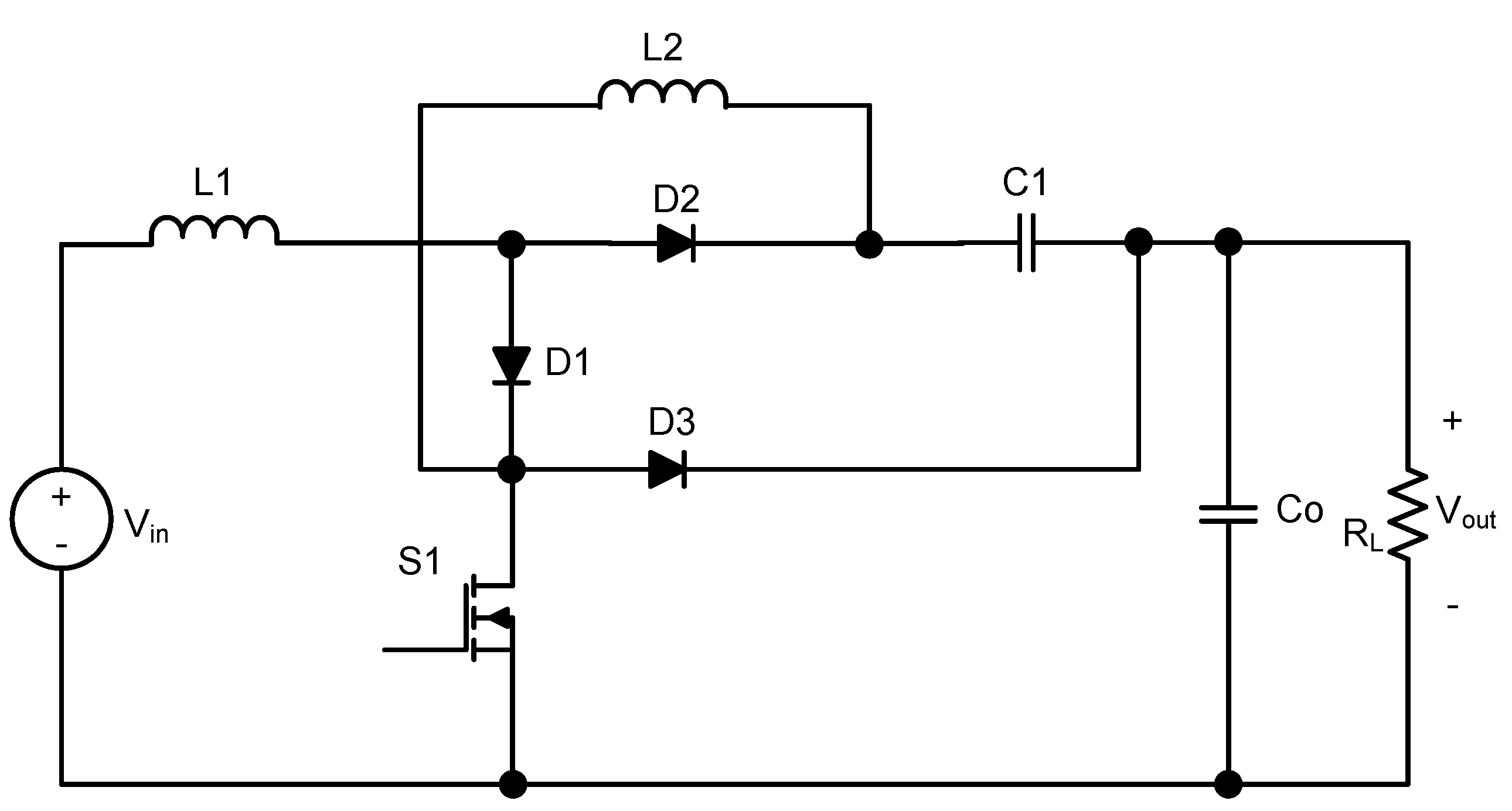
The DC-DC boost converter proposed in this paper has one power switch, which is a power MOSFET, three diodes, two inductors, and two capacitors. The topology of this converter is presented in Figure 1. Due to the existence of only one switch, the converter operates in two switching modes: Mode 0 (M0) and Mode 1 (M1). Proposed converter operates in a continuous conduction mode (CCM) and is capable of driving a wide range of resistive loads.
2.1. During M0
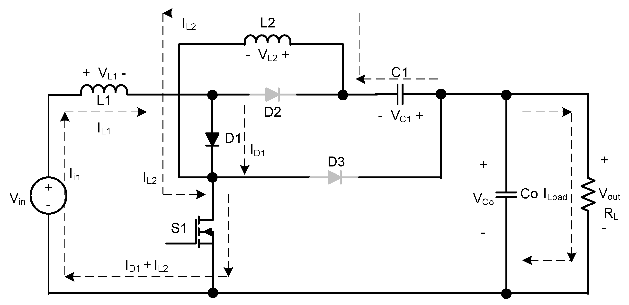
The MOSFET S1 is turned on, and diode D1 is forward biased and hence starts conducting. This causes the linear flow of current through the inductor L1, and hence the energy is stored in it. This condition is represented in Figure 2. After passing the short-lived transient phase, inductor L2 is also magnetized by the current . The directions of and are shown in Figure 2. Power diodes D2 and D3 are off, due to the reverse voltage polarity across them and hence do not conduct. The reason that capacitor C1 is in series with the inductor L2, is that the current also charges C1 with the voltage polarity, as shown in Figure 2. The current that flows through S1 is the algebraic sum of and .
The voltage across the inductor L1, , is only equal to the input DC voltage , as shown in Figure 2.
The voltage across L2, , is the same as the voltage across C1, . Hence,
2.2. During M1
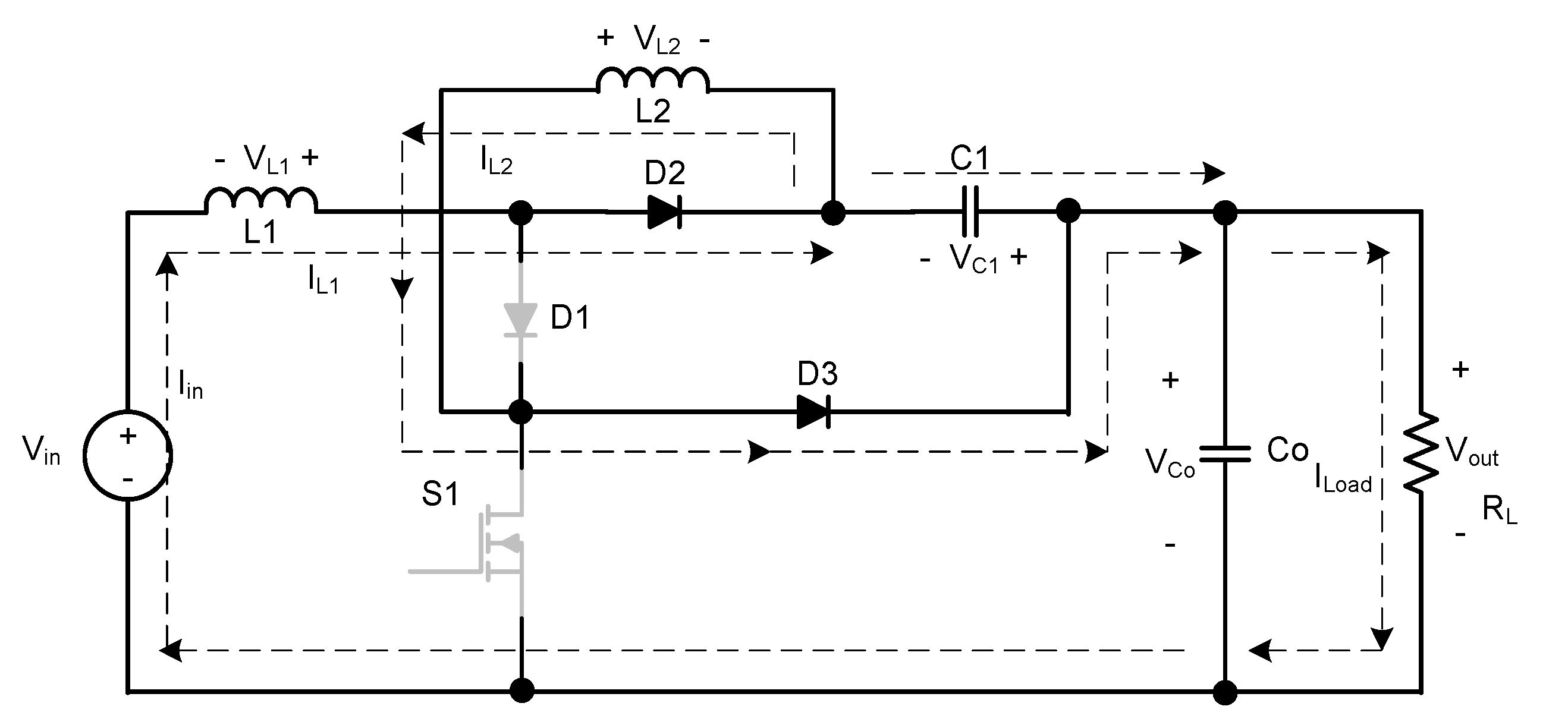
The switch S1 is turned off and the polarity across both L1 and L2 is reversed to maintain the current flow in the same direction as in M0. In this mode, diode D1 is off, due to the reverse bias polarity across it, and diodes D2 and D3 are on, as has been shown in Figure 3.
The energy that was stored in L1 and L2 is now released and transferred to the capacitors C1 and Co. Capacitor Co starts charging by developing the voltage across it according to the polarity shown in Figure 3. During M1, the voltage across L1 is the difference of the input DC voltage and the voltage across C1. Additionally, the voltage across L2 is the difference between and .
These relationships are represented as,
From (1),
During M0, the time differential is equal to the , where D is the duty-cycle and T is the switching period of the S1.
Hence,
Moreover, from (3),
3. Steady-State Analysis
The proposed converter operates in the CCM mode of operation even when heavily loaded. Assuming that the proposed converter operates in CCM mode and all the components used in the implementation are ideal, the analysis of the steady-state voltage gain, voltage stresses across the MOSFET, and all the diodes, as well as the efficiency is presented in the subsequent text.
3.1. DC Voltage Gain
Applying volt-second balance on (5) and (6) for L1 gives,
or,
From (2),
and from (4),
Applying the volt-second balance on (8) and (9) for L2 gives,
From Figure 3, it is obvious that the voltage across the output capacitor Co and the output voltage across the load is the same quantity; therefore, the output voltage can be replaced with . This leads to the following equation.
Using (7), the voltage across C1 can be calculated from the above equation, in terms of the duty-cycle D and the input voltage , as given below.
Putting the value of from (11) into (10), the steady-state DC voltage gain, G, of the proposed converter can then be derived, and is given by
The steady-state DC voltage gain transfer function of the proposed high-gain DC-DC boost converter given in (12), reveals that the output voltage is inversely proportional to the square of duty-cycle. Hence, increasing the duty-cycle value in (12) increases the output voltage quadratically, which validates the voltage boosting operation of the proposed DC voltage boost converter.
3.2. Voltage Stresses
When S1 is off in M1, the diode D2 becomes on and the S1 becomes parallel to the load. Therefore, the voltage across S1 is the same as .
When D1 is off, the voltage stress across D1, , can be calculated by applying the KVL around the loop, consisting of D3, , and L1. This gives
The voltage stress across D2 can be calculated by the condition when D2 is off in M0. It can be observed from Figure 2 that
The voltage stress, , can be calculated by applying the KVL around the loop consisting of D3, S1, and Co during M0. As S1 is on, the voltage across D3 during its off state is the voltage across Co, the . Hence,
3.3. Efficiency Analysis
The total power loss in the MOSFET is the sum of the static loss and the dynamic loss. Static power loss occurs in the MOSFET due to the channel resistance when the device is on; whereas dynamic power loss occurs due to the switching of the device. The static power loss in the MOSFET can be calculated as
In (17), is the on-state resistance of the transistor and is the rms current flowing through it. Dynamic loss for one switching period is given as
Hence the total power loss in the switch is given as
The power loss in a diode is the sum of the power loss due to the forward voltage drop and due to the on-state resistance under forward bias. The power loss in a diode can then be given as
In (20), is the forward voltage drop of the diode, is the forward junction resistance, and is the average current flowing through the diode under the on state. Power loss in a capacitor can be calculated as
In (21), ESR is the “equivalent series resistance” and is the rms value of capacitor current. Identically, the power loss, , in an inductor can be calculated as
In (22), the is the series resistance of the material the inductor is made form, and is the rms value of the current flowing through it. Hence, the total power loss in the proposed converter design will then be
The efficiency can be given as
4. Designing of the Passive Components
Selection of the values of the energy storing component is a critical factor in the behavior and performance of DC-DC converters, no matter which topology is used. The tolerance level in the ripple current of inductors and the ripple voltage of capacitors affects the smoothness and regulation in the output DC voltage levels. As a rule of thumb, the allowable maximum ripple in the inductor current should be no more than 10% of the maximum current that would flow through the inductor. Similarly, the maximum tolerable ripple in the voltage across a capacitor should be no more than 10% of the maximum voltage that will develop across the capacitor.
These assumptions set a fair principle for calculating the size of inductors and capacitors for a stable design that produces a smooth level of voltage across the load and provides a constant current. This principle is reflected in the calculations of the inductors and capacitor values used in this proposed boost converter.
4.1. Design of Inductor L1
The voltage developed across an inductor can be calculated using
Hence, the current through the inductor L1 is given as
Similarly, the current through inductor L2 is given as
The voltage across capacitor C1 is given by
or
or
From (27),
Comparing (28) and (29) gives
Rewriting (26) for L1
and in terms of and
The relation given in (32) gives the minimum value for L1 inductor that could be used. The is the ripple in the L1 inductor current, is the switching frequency of the power switch, is the output DC voltage of the converter, and D is the duty-cycle.
4.2. Design of Inductor L2
From (30),
or
and in terms of ,
(34) and (35) give the minimum L2 inductor value that is required in terms of and , respectively, with being the ripple level in L2 current.
4.3. Design of Capacitor C1
During Mode 0, the L2 and C1 are in series and the current through this branch is given as,
During Mode 0, the above equation takes the form
Using the relation
Hence (36) becomes
or
The relationship given in (38) gives the minimum value of C1 that can be used with ripples in the voltage across C1.
4.4. Design of Capacitor Co
The current through the capacitor C2 is given by
During Mode 0
The relationship presented in (39) gives the minimum output capacitor value with ripples in the output voltage. If switching frequency, the output voltage ripple and output capacitor current are kept constant, then the upper limit of the output capacitor is set by the duty-cycle of the converter. This leads to designing the output capacitor by operating the converter at the maximum permissible duty-cycle.
5. Results
This section describes the results and outcomes of the proposed boost converter. A PSIM simulation diagram and various relationships among the different parameters are presented in the form of graphs and tables to substantiate the proposed objectives of this research.
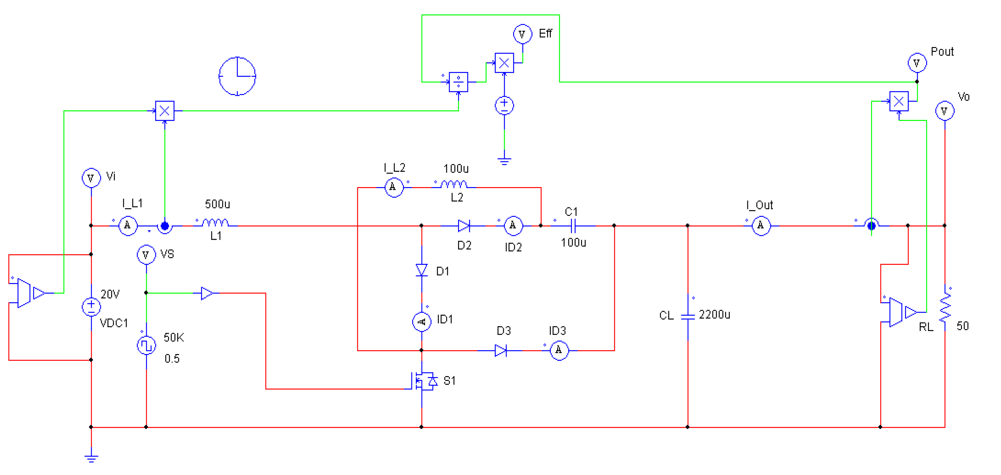
The proposed converter was simulated using PSIM to verify the relationships derived in Section 3 and presented in (12)–(16) and (24). All the components used in the implementation of the proposed design were assumed ideal.
Figure 4 shows the PSIM implementation of the proposed high-gain DC-DC boost converter, along with different virtual instruments which were used to measure the circuit parameters during the simulation. All the component values displayed in the schematic diagram are in standard units.
The values of the energy storage elements were set as: L1 = 400 µH, L2 = 100 µH, C1 = 100 µF, and Co = 2200 µF. The switching frequency of the power switch was set at 50 KHz. Simulation results were obtained with different input DC voltages, ranging from 5 V to 50 V and with different values of load resistance, ranging from to .
5.1. Operating Modes of the Proposed Converter
The proposed converter is intended to be used in a wide array of applications that range from PV grids to hybrid vehicles. Such applications demand that the converter operates in a continuous-conduction mode (CCM).
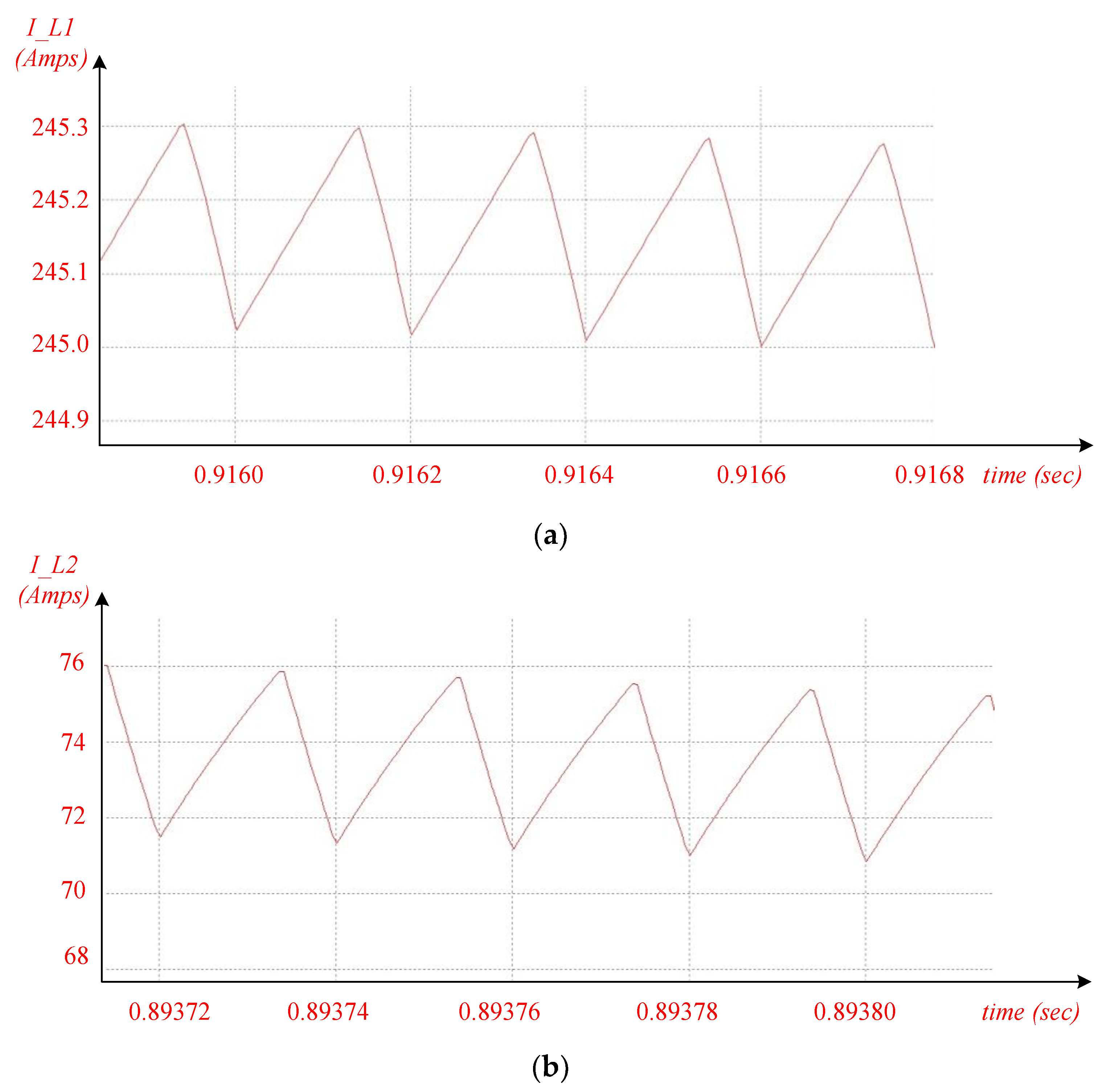
The proposed boost converter operates promisingly in CCM, even when it is loaded heavily to maintain the smooth flow of power to the load. Therefore, all the relationships derived in Section 3 are validated. The current waveforms through the inductors L1 and L2 are shown in Figure 5.
Currents through both the inductors, L1 and L2, do not completely cease during a switching cycle and hence prevent the converter from entering discontinuous-conduction mode (DCM).
5.2. Output DC Voltage
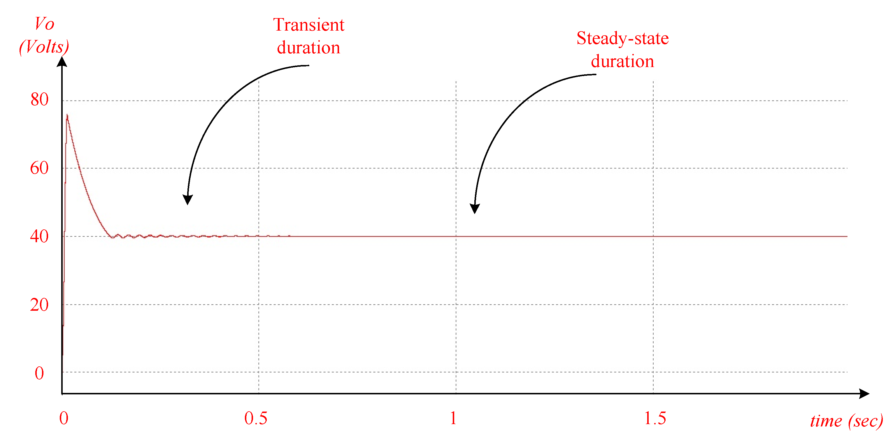
Simulation response of the voltage gain, shown in Figure 6, demonstrates that the converter remained in the transient state for less than 0.2 s and enters quickly into the steady-state phase.
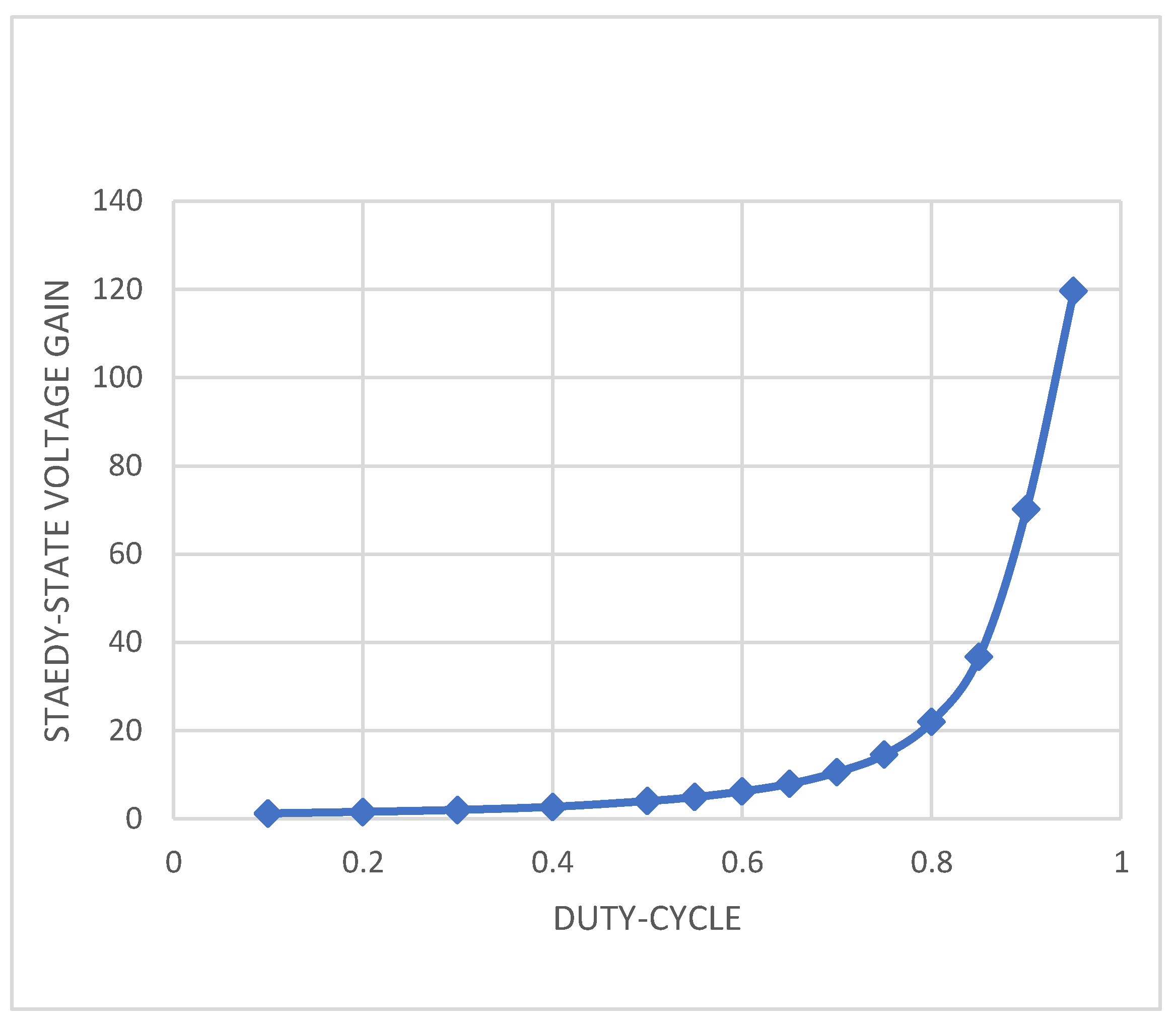
The simulation results revealed that the proposed converter follows the steady-state voltage gain relationship, for the duty-cycle range of .
5.3. DC Voltage Stress
The simulation results promisingly satisfied the relationships derived in (13)–(16) over the effective range of the duty-cycle. Table 1 shows a mutual comparison of the theoretical results with the PSIM simulation results for semiconductor devices S1, D1, D2, and D3.
5.4. DC Voltage Gain vs. Duty-Cycle Response
Figure 7 shows a graph of the steady-state DC voltage gain response of the proposed converter against the duty-cycle ranging from 0.1 to 0.95.
A 250 Watts prototype of the proposed boost converter with a 50 kHz switching frequency was configured for the most practical parasitic values of the components used in the modeling. These values are given as: the of the MOSFET was set to , the forward voltage drop for each diode was set to 0.6 V, ESR for each capacitor was set to , and the series resistance for each inductor coil was set to .
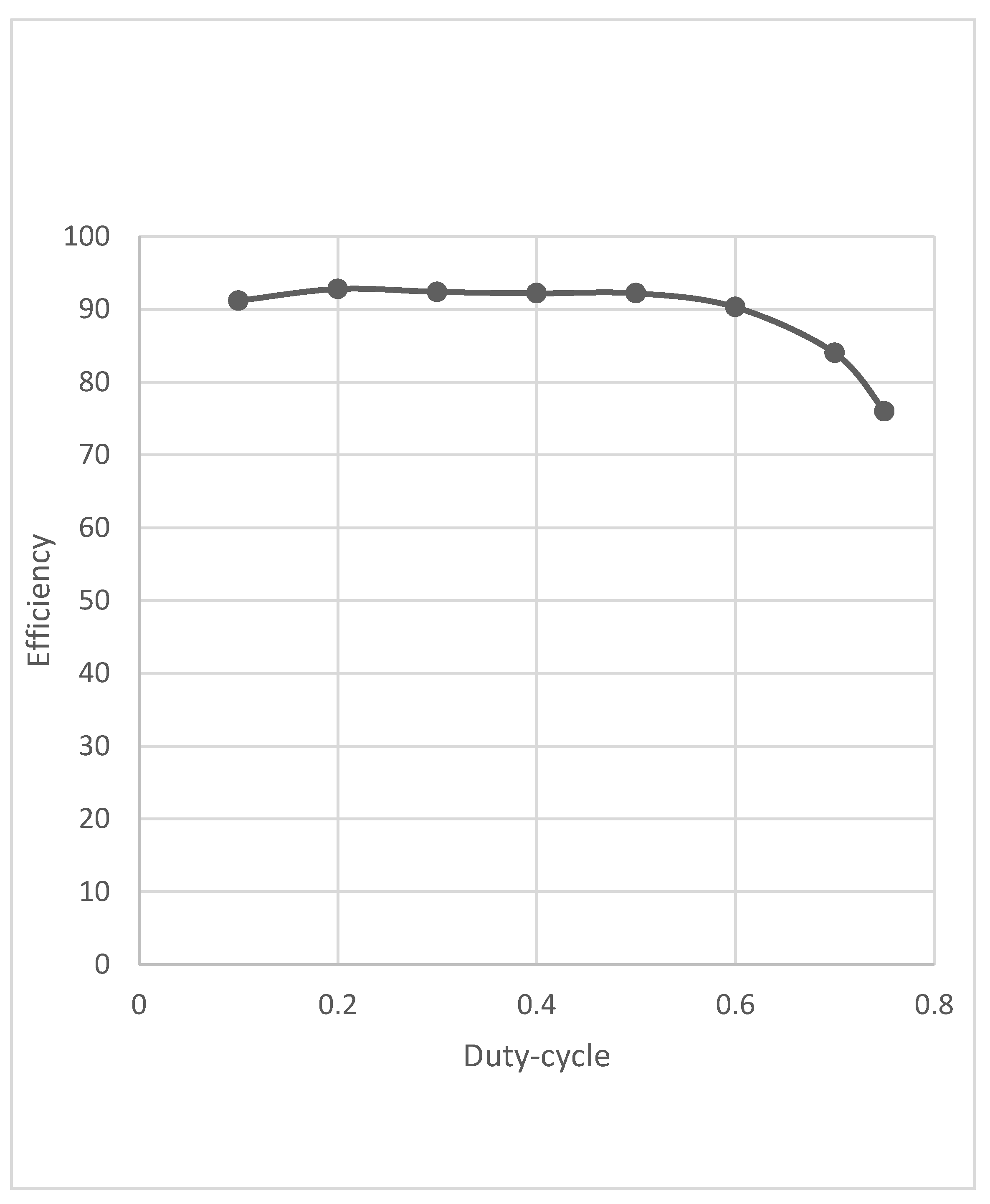
5.5. Efficiency vs. Duty-Cycle Response
The efficiency versus duty-cycle relationship over the effective range of duty-cycle for the 250 Watts prototype is shown in Figure 8. The graph shown in Figure 7 highlights that the proposed converter performed with more than 90% efficiency over a wide range of duty-cycles . Moreover, the proposed converter design can perform at a higher efficiency in comparison with the design presented in [9], when operated for high output. This feature marks its significance as a high-gain voltage boost structure for use in hybrid vehicles.
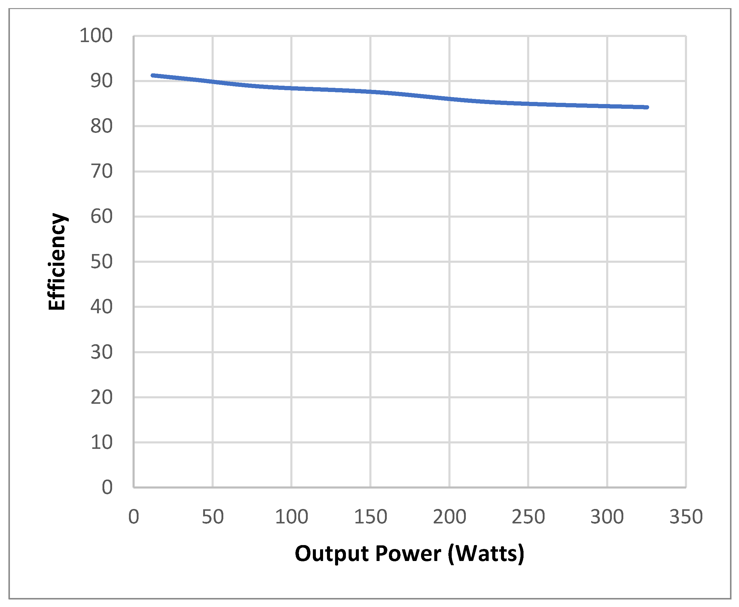
5.6. Efficiency vs. Output Power Response
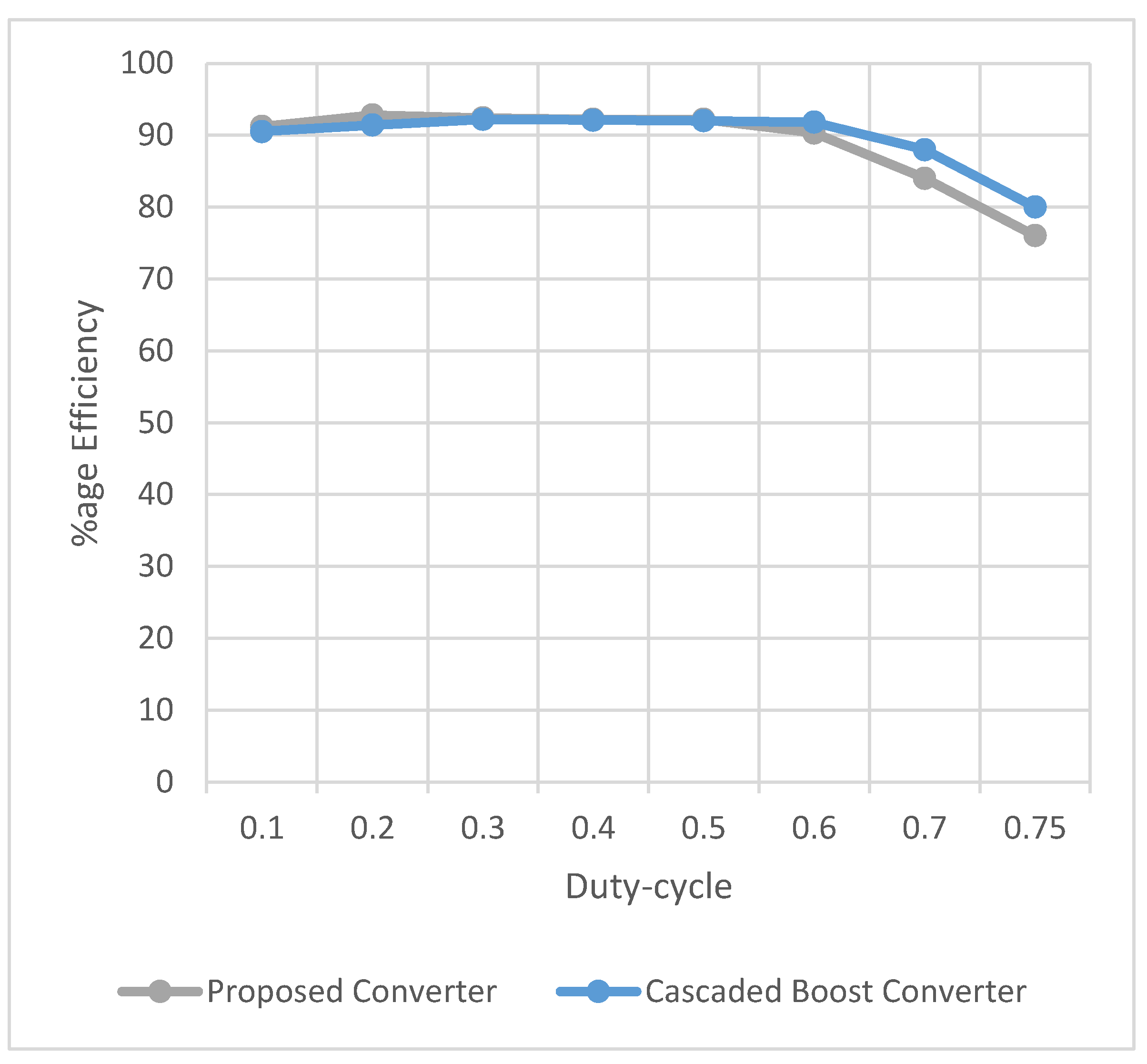
5.7. Efficiency Comparison with Cascaded-Boost Converter
A cascaded DC-DC boost converter is merely an integration of two conventional DC-DC boost converters, such that the output of the first converter is directly fed to the input of the next converter. This topology has been obligated by the fact that the total gain of two cascaded systems is the product of their individual gains. An efficiency comparison of the 250 Watts prototype of the proposed converter and a cascaded boost converter is presented in Figure 10.
These prototypes were simulated using PSIM. The comparison presented in Figure 10 shows that the proposed converter is no less efficient than the cascaded converter, even for high duty-cycles. The use of a single power switch makes the proposed converter more efficient while operated at a lower duty-cycle. Operating the converter at a lower duty-cycle allows the switch to remain off for most of the time during its switching period, and hence the average on-state voltage drop across the switch is reduced. Moreover, diodes that do not conduct during the ON state of the power switch do not dissipate any noticeable power. Therefore, power dissipation in the form of heat is reduced considerably, and, ultimately, the efficiency of the converter increases. In this proposed converter, the efficiency is higher than the cascaded converter for lower duty-cycles, without compromising the DC voltage gain, as evident from Figure 10.
The efficiency curve of the proposed converter also implies that this new design can be integrated in cascade with its replica to achieve even higher DC voltage gain. This approach will be helpful when both the cascaded converters are operated at a relatively low duty-cycle.
6. Discussion
The DC-DC voltage boost converters presented in [9,10,11] have many widespread advantages for modern switch-mode converter application domains, such as fuel cells and renewable energy. It was concluded from this research that the high-voltage gain is achieved by the integration of different voltage lifting techniques in these and other recently proposed boost converter designs.
A relative comparison based on the component count and the steady-state gain among the designs proposed in [9,10,11], the cascaded boost, and the design proposed in this research is presented in Table 2. Data presented in Table 2 show that the new high-voltage gain DC-DC boost converter proposed in this paper has a significantly lower component count compared to the other similar designs, without a considerable compromise in the DC voltage gain.
7. Conclusions
In this paper a new DC-DC boost converter is presented that utilizes a low component count in comparison to some recently proposed high DC voltage gain boost converters. The proposed boost converter was simulated for the DC voltage gain, voltage stresses, and efficiency. The simulation results proved the validity of the proposed design.
A 250 Watts prototype model was designed and simulated, and the results were compared with very recently published designs of boost converters, based on component count and component sizing. The comparison clearly revealed that the proposed design promisingly met the objective of achieving high-voltage gain, while keeping the component count low.
Author Contributions
Author contributions: The conceptualization and idea of the converter were generated by U.R. and A.F.M., H.A.S. provided the formal analysis and confirmation of mathematical modeling. D.G. provided help in reviewing the overall concept, its conceptual validation, and handling, plus submission of manuscript to the journal. All authors have read and agreed to the published version of the manuscript.
Funding
This research received no external funding.
Acknowledgments
The authors extend their appreciation to Mechatronics Laboratory (LIM) for their role as a meeting point and for knowledge sharing.
Conflicts of Interest
The authors declare no conflict of interest.
References
- Shahir, F.M.; Babaei, E. Extended topology for a Boost DC-DC Converter. IEEE Trans. Power Electron. 2019, 34, 2375–2384. [Google Scholar] [CrossRef]
- Bhaskar, M.S.; Almakhles, D.J.; Padmanaban, S.; Blaabjerg, F.; Subramaniam, U.; Ionel, D.M. Analysis and Investigation of Hybrid DC–DC Non-Isolated and Non-Inverting Nx Interleaved Multilevel Boost Converter (Nx-IMBC) for High Voltage Step-Up Applications: Hardware Implementation. IEEE Access 2020, 8, 87309–87328. [Google Scholar] [CrossRef]
- Ferdowsi, A.M.; Shamsi, P. A Family of Scalable Non-Isolated Interleaved DC-DC Boost Converters with Voltage Multiplier Cells. IEEE Access 2019, 7, 11707–11721. [Google Scholar] [CrossRef]
- Jiang, W.; Chincholkar, S.H.; Chan, C.-Y. Investigation of a Voltage-Mode Controller for a dc-dc Multilevel Boost Converter. IEEE Trans. Circuits Syst. II Express Briefs 2018, 65, 908–912. [Google Scholar] [CrossRef]
- Nguyen, M.-K.; Duong, T.-D.; Lim, Y.C. Switched-Capacitor-Based Dual-Switch High-Boost DC–DC Converter. IEEE Trans. Power Electron. 2018, 33, 4181–4189. [Google Scholar] [CrossRef]
- Khaligh, A.; Li, Z. Battery, Ultracapacitor, Fuel Cell, and Hybrid Energy Storage Systems for Electric, Hybrid Electric, Fuel Cell, and Plug-In Hybrid Electric Vehicles: State of the Art. IEEE Trans. Veh. Technol. 2010, 59, 2806–2814. [Google Scholar] [CrossRef]
- Lai, C.-M.; Cheng, Y.-H.; Hsieh, M.-H.; Lin, Y.-C. Development of a Bidirectional DC/DC Converter with Dual-Battery Energy Storage for Hybrid Electric Vehicle System. IEEE Trans. Veh. Technol. 2017, 67, 1036–1052. [Google Scholar] [CrossRef]
- Forouzesh, M.; Siwakoti, Y.P.; Gorji, S.A.; Blaabjerg, F.; Lehman, B. Step-Up DC–DC Converters: A Comprehensive Review of Voltage-Boosting Techniques, Topologies, and Applications. IEEE Trans. Power Electron. 2017, 32, 9143–9178. [Google Scholar] [CrossRef]
- Pires, V.F.; Cordeiro, A.; Foito, D.; Silva, J.F. High Step-Up DC-DC Converter for Fuel Cell Vehicles Based on Merged Quadratic Boost-Cuk. IEEE Trans. Veh. Technol. 2019, 68, 7521–7530. [Google Scholar] [CrossRef]
- Zhang, Y.; Liu, H.; Li, J.; Sumner, M.; Xia, C. DC–DC Boost Converter With a Wide Input Range and High Voltage Gain for Fuel Cell Vehicles. IEEE Trans. Power Electron. 2018, 34, 4100–4111. [Google Scholar] [CrossRef]
- Ferdowsi, A.A.M.; Shamsi, P. High-Voltage-Gain DC-DC Step-Up Converter with Bifold Dickson Voltage Multiplier Cells. IEEE Trans. Power Electron. 2019, 34, 9732–9742. [Google Scholar]
Figure 1.
Topology of the proposed DC-DC boost converter.

Figure 2.
Voltage polarities and current directions in Mode 0.

Figure 3.
Voltage polarities and current directions in Mode 1.

Figure 4.
PSIM implementation schematic of the proposed converter.

Figure 5.
Current waveforms of the inductors: (a) L1, and (b) L2.

Figure 6.
Output voltage simulation waveform for D = 0.75.

Figure 7.
Steady-state voltage gain vs. duty-cycle response.

Figure 8.
Efficiency versus duty-cycle plot of the 250 Watts prototype.

Figure 9.
Efficiency versus output power plot of the proposed converter.

Figure 10.
Efficiency comparison of the proposed and a cascaded boost converter.


Table 1.
Voltage stresses across different components at different duty-cycles.
| D | S1 | D1 | D2 | D3 | ||||
|---|---|---|---|---|---|---|---|---|
| (13) | PSIM | (14) | PSIM | (15) | PSIM | (16) | PSIM | |
| 0.1 | 12.34 | 12.34 | 1.22 | 1.24 | 11.24 | 11.12 | 12.34 | 12.34 |
| 0.2 | 15.62 | 15.61 | 3.12 | 3.15 | 12.8 | 12.5 | 15.62 | 15.61 |
| 0.3 | 20.4 | 20.44 | 6.11 | 6.07 | 14.42 | 14.35 | 20.4 | 20.44 |
| 0.4 | 27.8 | 27.8 | 11.22 | 11.2 | 16.8 | 16.67 | 27.8 | 27.8 |
| 0.5 | 40 | 40.1 | 20.2 | 20.17 | 20.24 | 20.01 | 40 | 40.1 |
| 0.6 | 62.5 | 62.5 | 37.51 | 37.44 | 27.2 | 26.6 | 62.5 | 62.5 |
| 0.7 | 111.11 | 111.11 | 78.11 | 78.08 | 39.24 | 38.33 | 111.11 | 111.11 |
| 0.75 | 160 | 159.8 | 113.82 | 113.8 | 39.88 | 38.31 | 160 | 159.8 |
Publisher’s Note: MDPI stays neutral with regard to jurisdictional claims in published maps and institutional affiliations. |
© 2021 by the authors. Licensee MDPI, Basel, Switzerland. This article is an open access article distributed under the terms and conditions of the Creative Commons Attribution (CC BY) license (https://creativecommons.org/licenses/by/4.0/).
Share and Cite
MDPI and ACS Style
Rafiq, U.; Murtaza, A.F.; Sher, H.A.; Gandini, D. Design and Analysis of a Novel High-Gain DC-DC Boost Converter with Low Component Count. Electronics 2021, 10, 1761. https://doi.org/10.3390/electronics10151761
AMA Style
Rafiq U, Murtaza AF, Sher HA, Gandini D. Design and Analysis of a Novel High-Gain DC-DC Boost Converter with Low Component Count. Electronics. 2021; 10(15):1761. https://doi.org/10.3390/electronics10151761
Chicago/Turabian StyleRafiq, Usman, Ali Faisal Murtaza, Hadeed A. Sher, and Dario Gandini. 2021. "Design and Analysis of a Novel High-Gain DC-DC Boost Converter with Low Component Count" Electronics 10, no. 15: 1761. https://doi.org/10.3390/electronics10151761
Note that from the first issue of 2016, this journal uses article numbers instead of page numbers. See further details here.