1. Introduction
Renewable energy is becoming increasingly important for future sustainability. Nowadays, photovoltaic (PV) systems are growing, with an estimated worldwide installed capacity of about 871 GW in 2022 [
1,
2]. A photovoltaic module converts solar irradiation into DC electrical energy. To connect a PV system to a load/grid, the DC voltage needs to be processed by means of a DC/DC or DC/AC power electronics converter. Different circuit configurations can be employed to connect PV panels to power converters, such as central or string arrangements [
3]. However, it has been verified that module-level power conversion, i.e., each PV module with an individual power converter, provides the best solar energy harvesting capability and the best tracking of the global maximum power point [
3,
4]. Regarding the converter topologies currently employed in the field of module-level power conversion, the flyback converter [
5,
6] is gaining popularity since it provides important benefits such as galvanic isolation, high power density, easy voltage step-up, and low number of components [
4]. Moreover, paralleling flyback units is a straightforward way to deal with the harmful mismatch effects among PV modules. However, for the flyback topology to be competitive with other circuit configurations, challenges related to the conversion efficiency and system reliability must be met [
7].
Several articles in the literature report the application of flyback converters to PV systems [
8,
9,
10,
11,
12,
13,
14,
15,
16]. Most of these works are based on an interleaved topology that consists of splitting a full converter into several standard flyback cells, each managing a part of the converter overall power [
15,
16].
An input-parallel output-parallel (IPOP) interleaved flyback converter is presented in [
8], where two flyback cells are considered, and a single-phase inverter is connected between the DC/DC stage and the grid. The reduction of the current ripple as well as the reduction of the size of the passive elements are mentioned as a contribution.
For the same IPOP interleaved flyback topology, in [
9], a control scheme based on selecting the operating mode of the flyback cells (discontinuous conduction mode (DCM), boundary conduction mode, or a combination of both) is proposed to optimize the efficiency. These operating modes are further investigated in [
10] for a grid-tied interleaved flyback microinverter, aiming to optimize the efficiency in a wide load range.
In [
11], an IPOP interleaved converter based on three flyback cells is presented. In this case, as the number of parallel DC/DC cells increases, the current ripple is reduced, as well as the size of the passive filtering element. An input-parallel output-series (IPOS) interleaved flyback converter is described in [
12]. This circuit configuration can achieve a higher output voltage compared to the IPOP topology; however, the output diodes’ current rating is rather high.
The integration of harmonic injection capability into an interleaved flyback inverter is thoroughly investigated in [
13]. This method is studied for the implementation of an active anti-islanding scheme. Moreover, a mathematical model is proposed to accurately predict the steady-state behavior of the converter, either in grid-tied or in islanding operation.
To obtain soft switching on the converter, an active clamp circuit is introduced in [
14], allowing a considerable reduction of the switching losses of the topology.
Regarding the application of DC-DC converters based on a single input and multiple outputs, different approaches can be found in the literature [
17,
18,
19,
20,
21,
22]. There are also approaches that use multiple winding transformers [
23,
24,
25], although those with a single input and multiple outputs are the most frequent uses.
The aims could be to supply several cascade-connected H-bridges to generate a multilevel AC output [
17,
18], to connect the output in series to obtain a high DC voltage [
19], or to supply independent loads with different voltage levels (depending on the number of turns of the secondary windings) [
20,
21,
22].
For converters with multiple inputs and a single output, in [
23], a two-input buck-boost converter is presented. One input receives power from the grid, whereas the other is connected to a PV array. The power of both inputs is combined to supply a resistive load. In [
24], a DC–DC topology that can be supplied by independent DC sources is shown. The DC input voltages are converted into AC voltages by means of half-bridge inverters, then a multi-winding transformer transfers the power from all the primary inputs to the secondary output where another half-bridge converter transforms the AC voltage into DC voltage to finally supply a load. A disadvantage is that the transformer should manage the total converter power, and the number of bulky capacitors will be two times the number of inputs. Finally, a multi-input DC–DC topology for renewable energy applications with battery backup is proposed in [
25]. The converter is based on the standard flyback topology, but additional diodes and an auxiliary switch are included to allow a safe switch between the renewable energy inputs and the batteries.
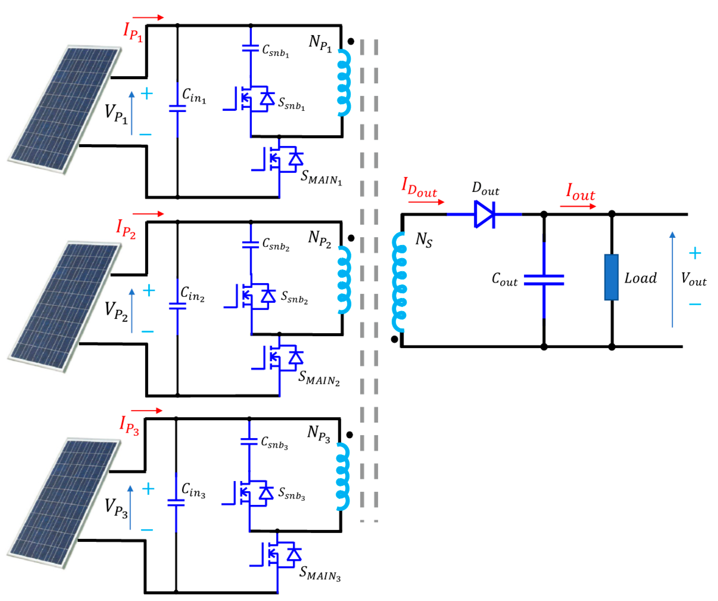
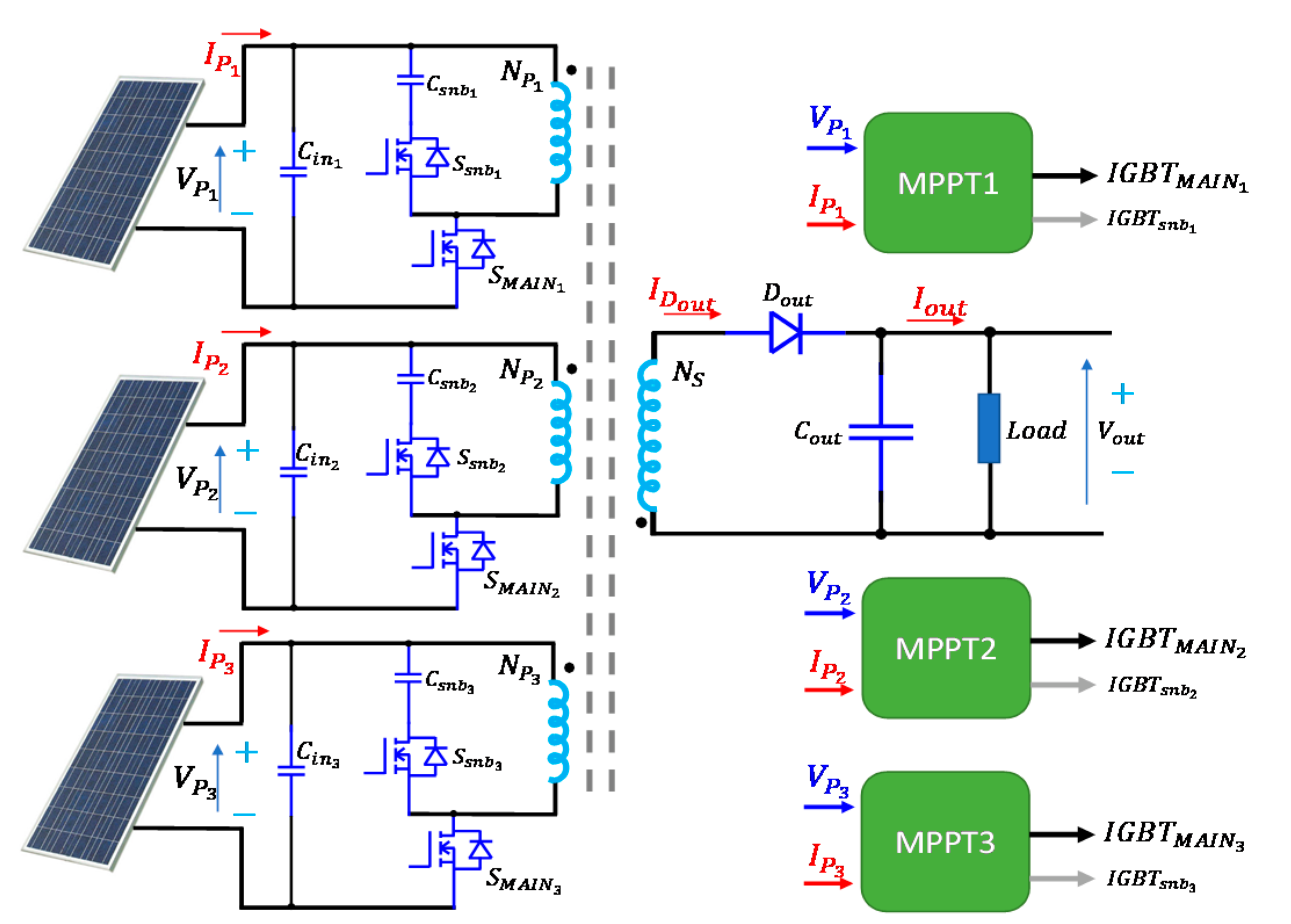
In this paper, a N-modules flyback interleaved power converter with parallel connected inputs and a single output is proposed for a PV generation system. The circuit configuration is built by using a single transformer (one core) with N primary windings and one secondary winding. This represents an advantage in terms of cost and volume compared to the conventional interleaved IPOS topology [
12], where the number of individual transformers (individual cores) equals the number of flyback modules. With this structure, the output diode operates N times more in a cycle (than conventional interleaved converters), and the output capacitor can therefore be smaller. For the classical problems of flyback topologies (leakage inductance) [
15], active snubber circuits are added to provide protection to the main switches against
during commutation. The snubber circuits return the energy of the leakage inductance to the input capacitor of the PV, then increasing the efficiency of the topology. The proposed power converter is depicted in
Figure 1 (with N = 3). More than three PV panels can be implemented in applications where it is required to increase the system power. The proposed converter is intended for applications with low input voltage and high current; the DC output voltage can be used to supply single-phase grid-tied inverters or hydrogen production with photovoltaic cells [
26,
27,
28,
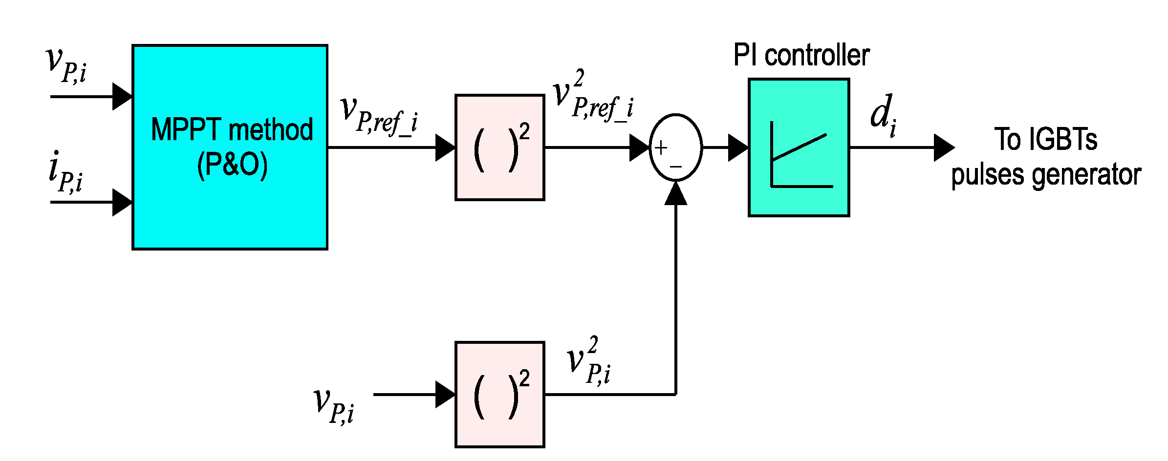
29]. On the other hand, a maximum power point tracking (MPPT) algorithm is implemented to extract the maximum power available in the PV modules [
30].
The rest of the work is organized as follows.
Section 2 thoroughly describes the operating principle of the converter.
Section 3 presents the implemented MPPT scheme. In
Section 4, guidelines about the transformer’s core design are presented, whereas in
Section 5 a description of the converter input capacitor design is reported. Simulations results are shown in
Section 6, and
Section 7 presents the obtained experimental results. In
Section 8, efficiency results are show. The conclusions of the work are stated in
Section 9.
2. Operating Principle
The analysis of the converter and its different operating modes was done under the following assumptions: semiconductor devices are ideal, single-core ferrite coupled inductors (flyback transformer) have unitary coupling coefficient and unity turns ratio (
, where
refers to the n-th primary windings); the resistances are neglected, and the leakage inductance is
; the converter operates in current discontinuous conduction mode (DCM) and steady state. Two duty cycles are defined:
for main switches (
) and
for the snubber switches (
. The magnetizing inductance is
, the switching frequency is
, and the commutation period is
. The general aspects of the operation of this topology were based on extracting the energy from the PV panels connected to the converter in a single switching period
. The flyback transformer was designed to manage the power from a single PV panel and not from all the panels together; this made it possible to reduce the size of the magnetic core. The switching period was divided in segments depending on the number of primary windings; hence, in this work,
was divided in three sections. The purpose of the snubber network was to recover the energy stored in the flyback transformer leakage inductance and limit the main switches
. The leakage inductance current charged the snubber capacitor, and then that current was returned to the input capacitor
through the antiparallel diode of the main switch. This process improved the efficiency of the topology. The operating principle consisted in six stages for each PV panel used. Since in this paper
is considered, the total number of stages per switching period was 18.
Figure 2,
Figure 3,
Figure 4,
Figure 5,
Figure 6 and
Figure 7 shows the first six stages per period, for the first PV panel. The main equation will be described for each state.
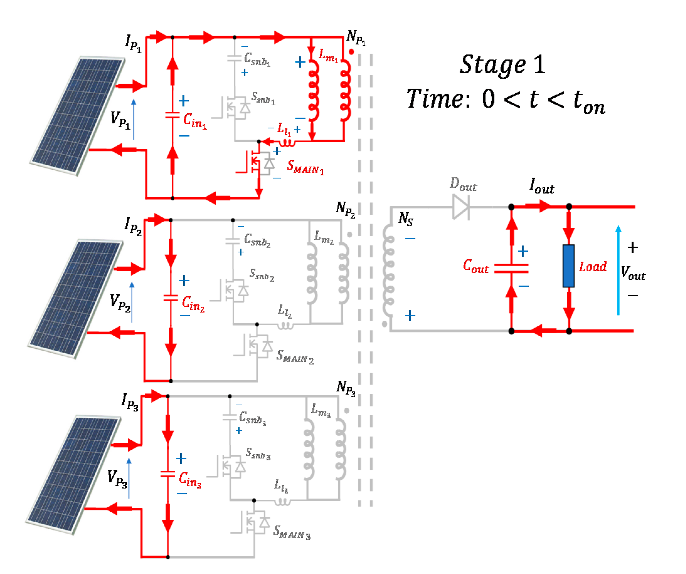
2.1. Stage 1:
As can be seen in
Figure 2, at this stage only
is activated. The energy extracted from PV panel 1 is stored in the magnetizing inductance
of the flyback transformer. The maximum and average currents in the switch are defined by (1) and (2), respectively. On the other hand, the snubber capacitor
is charged (from the previous cycle) to a voltage defined by Equation (3)
The average current of and the are zero for energy balance of the snubber circuit that absorbs energy from and delivers energy to . The output diode is turned off and does not transfer energy to the output capacitor .
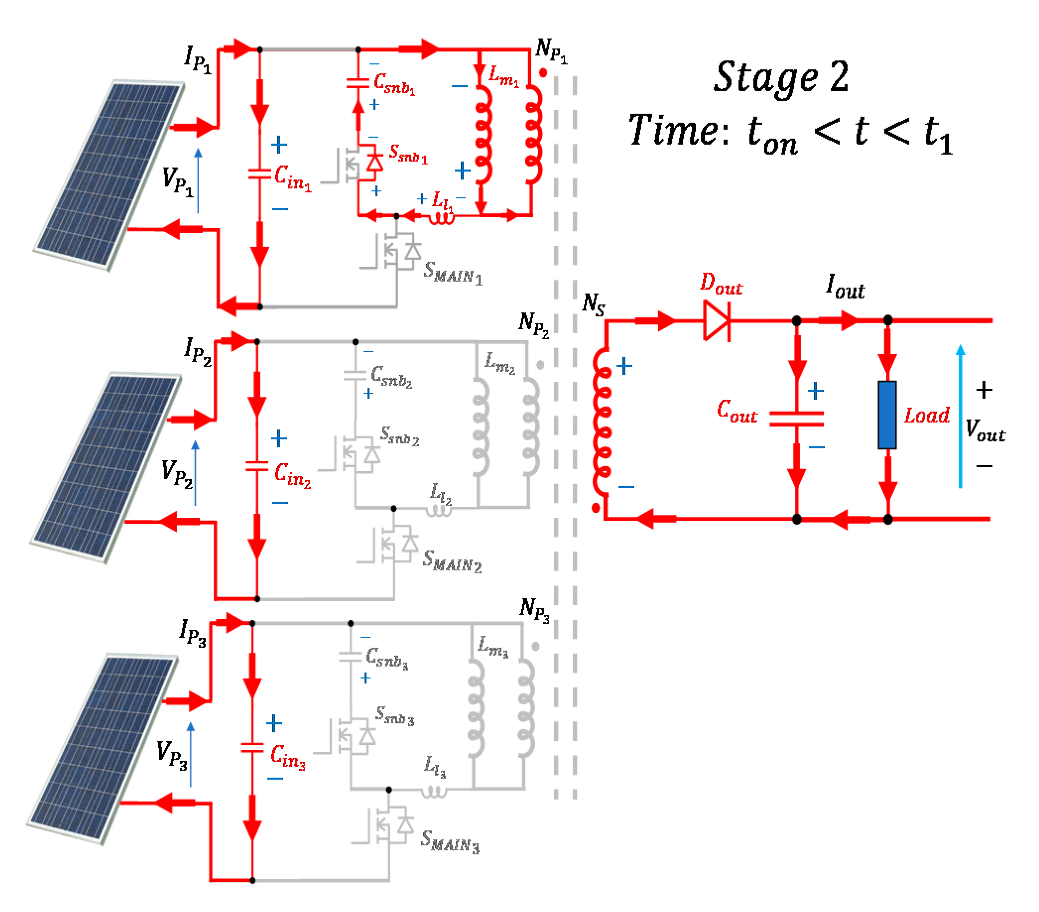
2.2. Stage 2:
Figure 3 shows the
turned off. The magnetizing current (defined by (4)) decreases and flows through the output diode
(defined in (5)) and the diode of the snubber switch
. The
diode conducts current from
to
through the leakage inductance
; this current is defined by Equation (6). The voltage in
increases and it is defined by Equation (7). On the other side, the diode
will be forward biased by the secondary winding, and a current will flow, charging the output capacitor
; this current is defined by Equation (5). Part of the magnetizing current is stored in the leakage inductor and flows into the snubber circuit. The voltage in the leakage inductance (Equation (7)) allows to define the snubber capacitor voltage expression in Equation (8). At
, the current in the snubber capacitor decreases to zero. In this stage, the magnetizing inductance voltage is
.
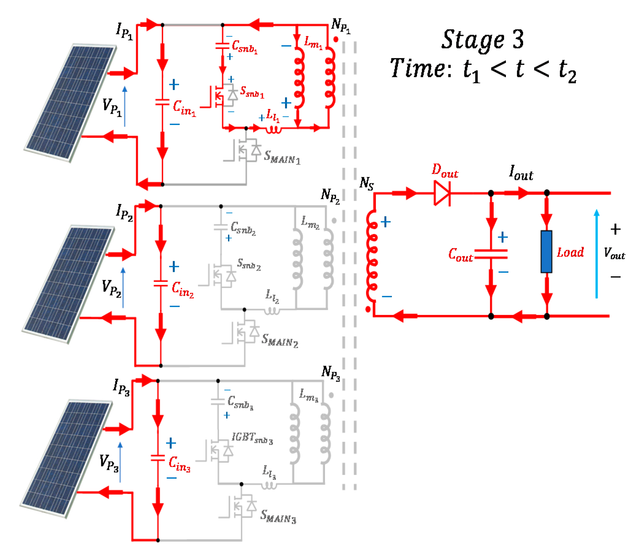
2.3. Stage 3:
In
Figure 4, only the device
is activated. The energy delivered by the leakage inductance
to the snubber capacitor
is now returned to the leakage inductance
. For energy balance, the average current in the snubber capacitor
is zero.
At
, the leakage inductance current, given by Equation (6), is maximum but it circulates in the opposite direction than in Stage 2. For
, the snubber capacitor recovers the initial voltage of Stage 1. The output diode current
is given by Equation (9), and the main switch blocking voltage is given by Equation (10).
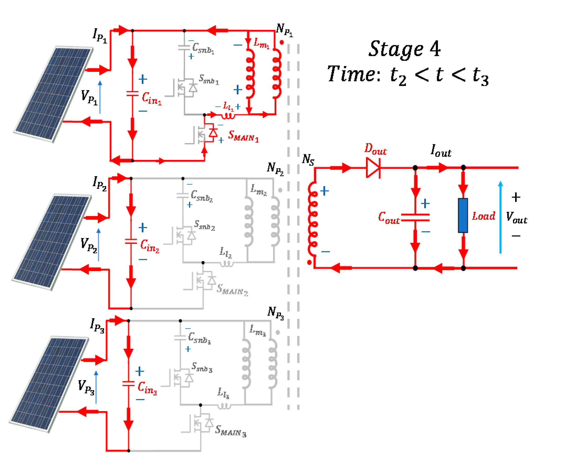
2.4. Stage 4:
Figure 5 shows that
is now disactivated. The leakage inductance current flows through the magnetizing inductance, the input capacitor
, and the diode of the main switch. The energy stored in the leakage inductance is returned to the input capacitor
, increasing the conversion efficiency. At
, the leakage inductance current decreases to zero, the leakage inductance voltage
is defined by Equation (11), and the time when the leakage inductance current decreases to zero can be calculated by Equation (12). In the secondary winding, the output diode current starts to decrease because the energy stored in the magnetizing inductance was delivered to the output capacitor. Additionally, this current also flows to the load.
2.5. Stage 5:
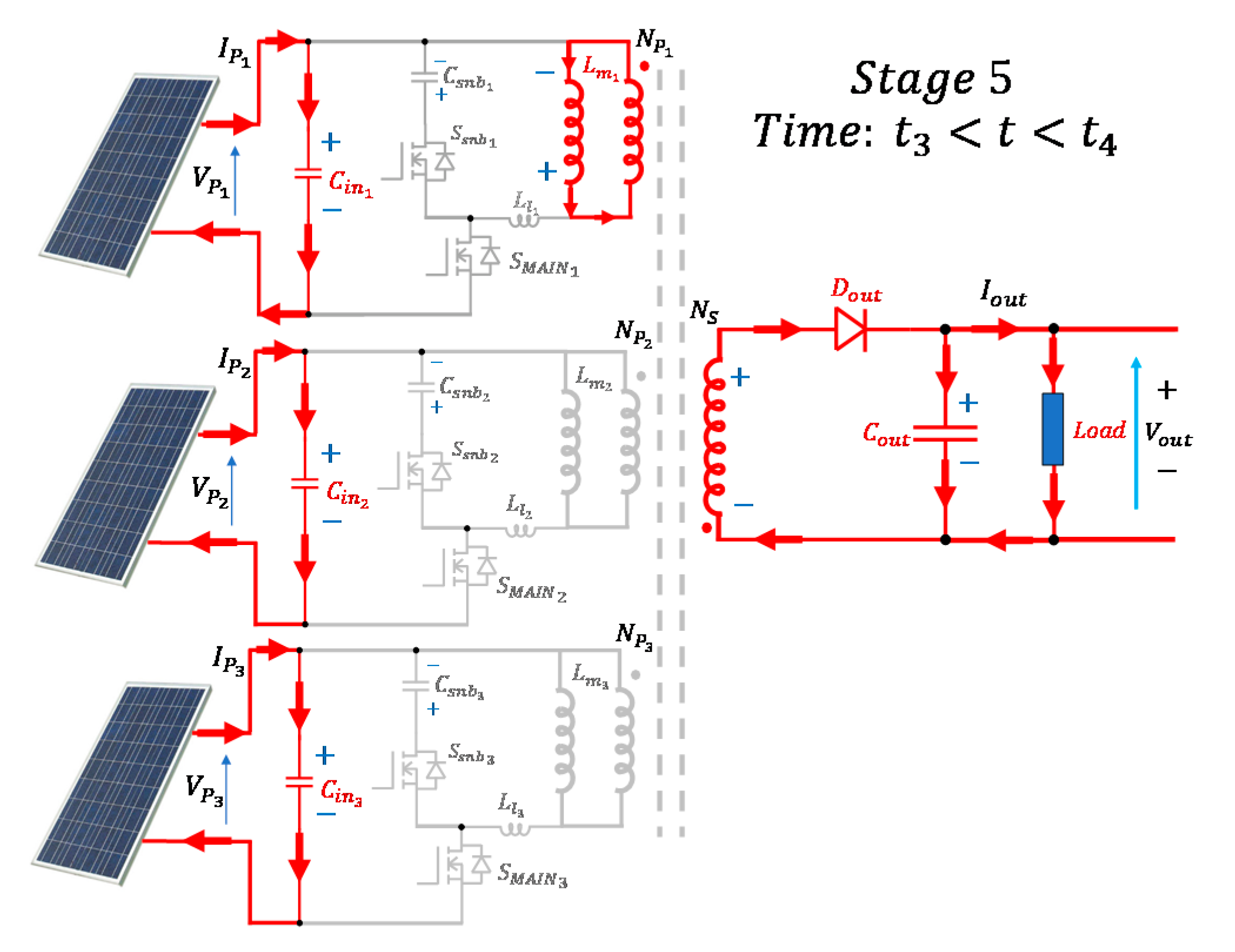
In
Figure 6,
and
are turned off. The output diode current decreases to zero at
. The output diode turn-on time is defined by Equation (13).
2.6. Stage 6:
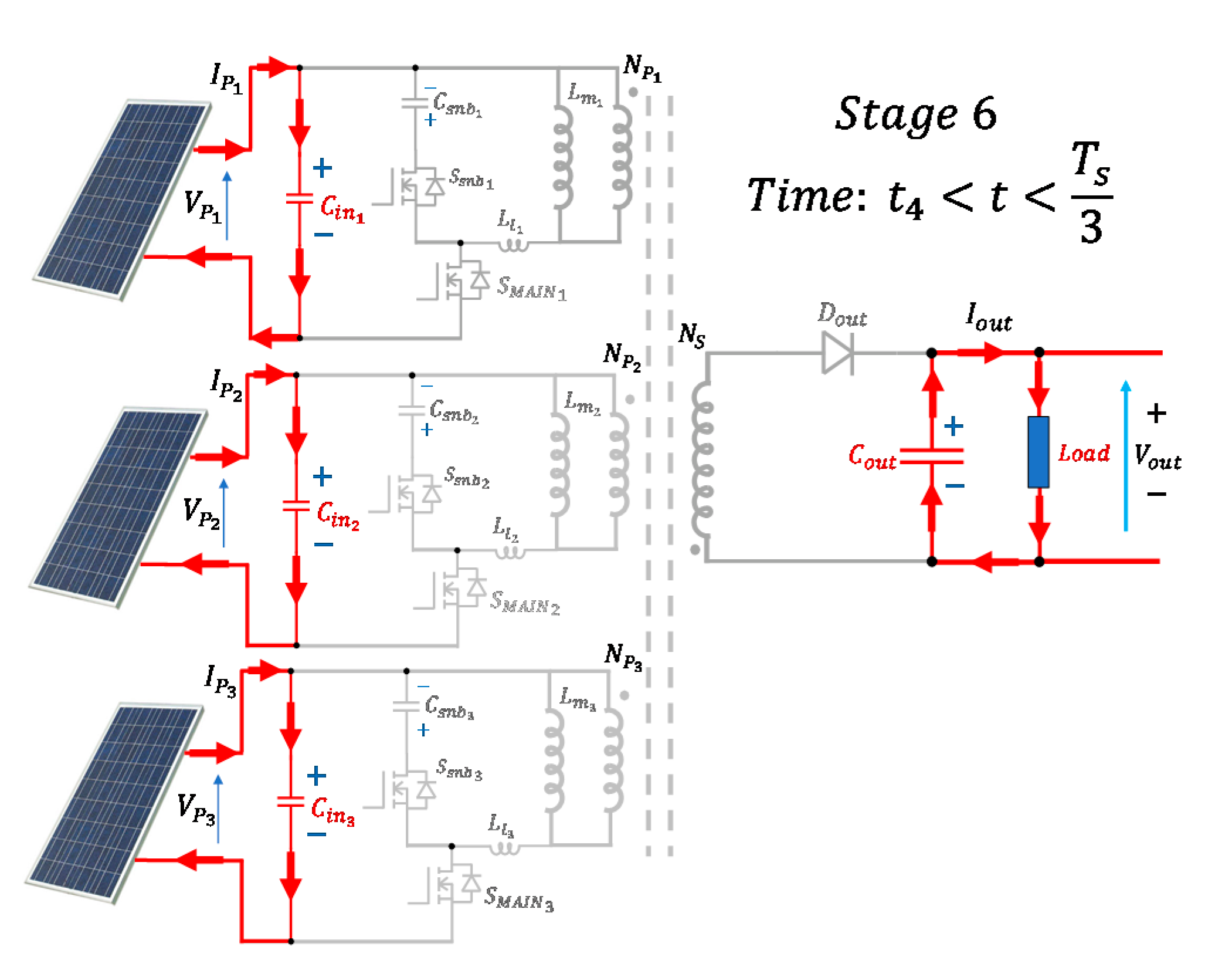
In
Figure 7, all the switches are deactivated. The energy stored in the output capacitor
is delivered to the load. The output capacitor current is defined by (14).
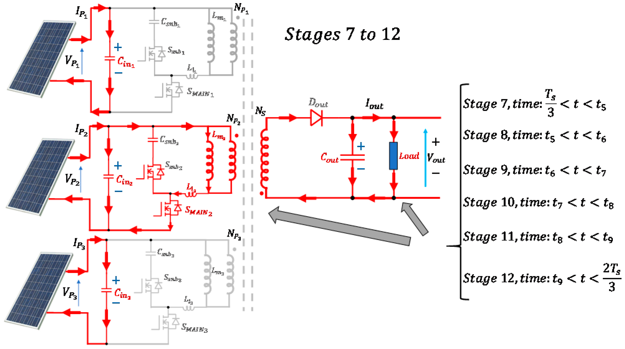
2.7. Stage 7 to 12:
The six stages described above consider the energy extraction from PV panel 1. Then, the next six stages, that is, from Stage 7 to Stage 12, will correspond to the energy extraction from PV panel 2 (
Figure 8). The energy extraction from PV panel 2 is similar to that performed in PV panel 1, and the operation mode is the same as described for the first six stages. Therefore, the equations are the same, but the time interval goes from
(for Stage 7) to
(for Stage 12).
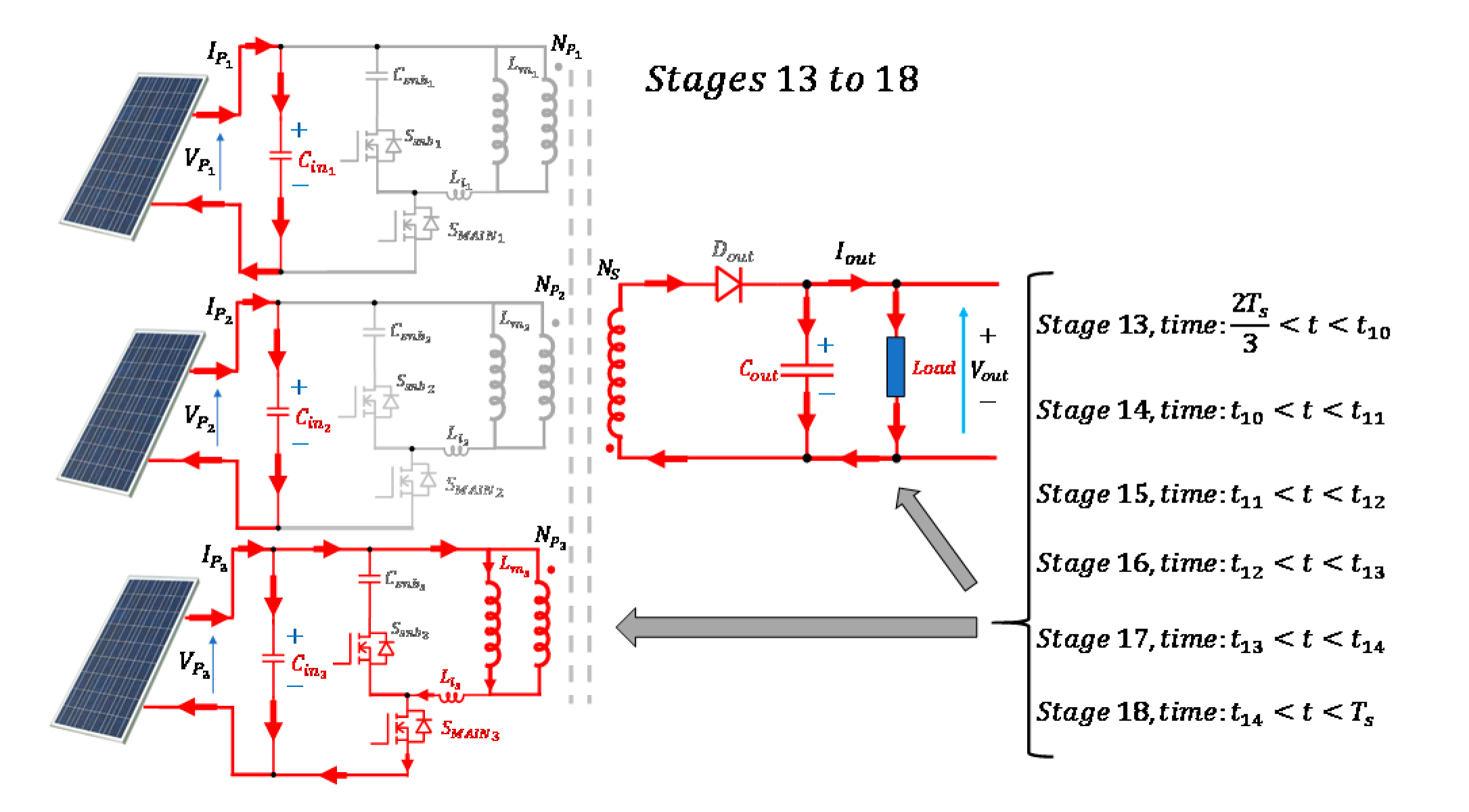
2.8. Stage 13 to 18:
For the final six stages, that is, from Stage 13 to 18, as shown in
Figure 9, energy extraction from PV panel 3 is carried out. Again, the operation and mathematical expressions are the same as described for the first PV panel, but now in a time interval from
(for Stage 13) to
(for Stage 18).
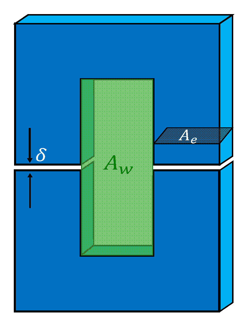
4. Flyback Transformer Core Design
In this work, the flyback transformer core considered a U-type-geometry ferrite-based core (N27 and N87 Siferrit
® materials). Joining two U-type magnetic cores, an O-type core is formed, obtaining two symmetrical air gaps, as can be seen in
Figure 12. According to this geometry, and considering the approach in [
31], the expression that relates the product of the areas of the window
and transversal
to the parameters of the circuit is defined by Equation (15), where
is the maximum duty cycle,
is the rms primary winding current,
is the differential magnetic density,
is the primary utilization factor,
is the utilization factor of the winding area, and
is the current density. Since the converter operated in DCM, the expression (15) can be rewritten in terms of the input power, obtaining Equation (16), where
is the input power of one PV panel. The expression that defines the air gap
in terms of input power is defined by Equation (17).
As can be seen in Equations (16) and (17), the input power is proportional to the product
and the air gap
. In the proposed topology, since each converter input module transferred energy to the secondary side during a period
, the average power processed by the transformer in a switching period
was only the one produced by a single PV panel, whereas the total power managed by the converter corresponded to that generated by the
PV panels (three in this work). Therefore, the core was designed to process only one-third of the total power. This is an advantage in terms of cost–volume compared to other flyback topologies where the transformer must be designed for the total converter power [
11,
12,
13,
16].
5. Input Capacitor Design
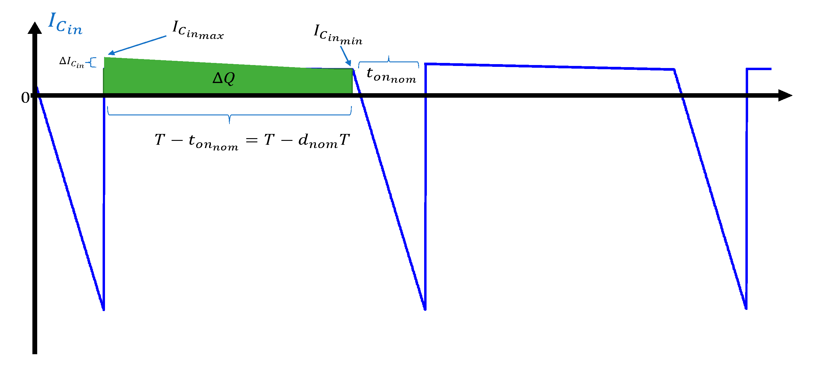
In this section, a brief analysis of the input capacitor is presented. In steady state and operating at rated power, the nominal duty cycle was approximately and the maximum duty cycle (limited by the switching period since three PV panels were being used) was . In this work, PV panels rated at 340 W and with nominal voltage and current of 37 V and 9.18 A, respectively, were used.
According to the current waveform in the input capacitor (in parallel with the PV panel), the area under the curve in the charging cycle must be equal to the discharge area due to the energy balance in the capacitor.
The area under the discharging curve (
Figure 13) is formed by the turned-off time of the main switch, and the maximum amplitude of the current is
, where
is the minimum capacitor current amplitude.
Assuming an ideal operation, in one commutation period, this area is equal to the average current delivered by a PV panel and defined by
. Thus,
is defined by Equation (18), and
is defined by Equation (19), where
is the PV panel voltage ripple desired:
6. Simulation Results
In this section, the simulation results are presented. The simulation parameters are shown in
Table 1. Each PV panel received different solar irradiance, i.e., PV1: 900 W/m
2, PV2: 1000 W/m
2, and PV3: 800 W/m
2. This allowed us to verify the operation of the topology and the MPPT algorithm, with different duty cycles for the individual flyback modules.
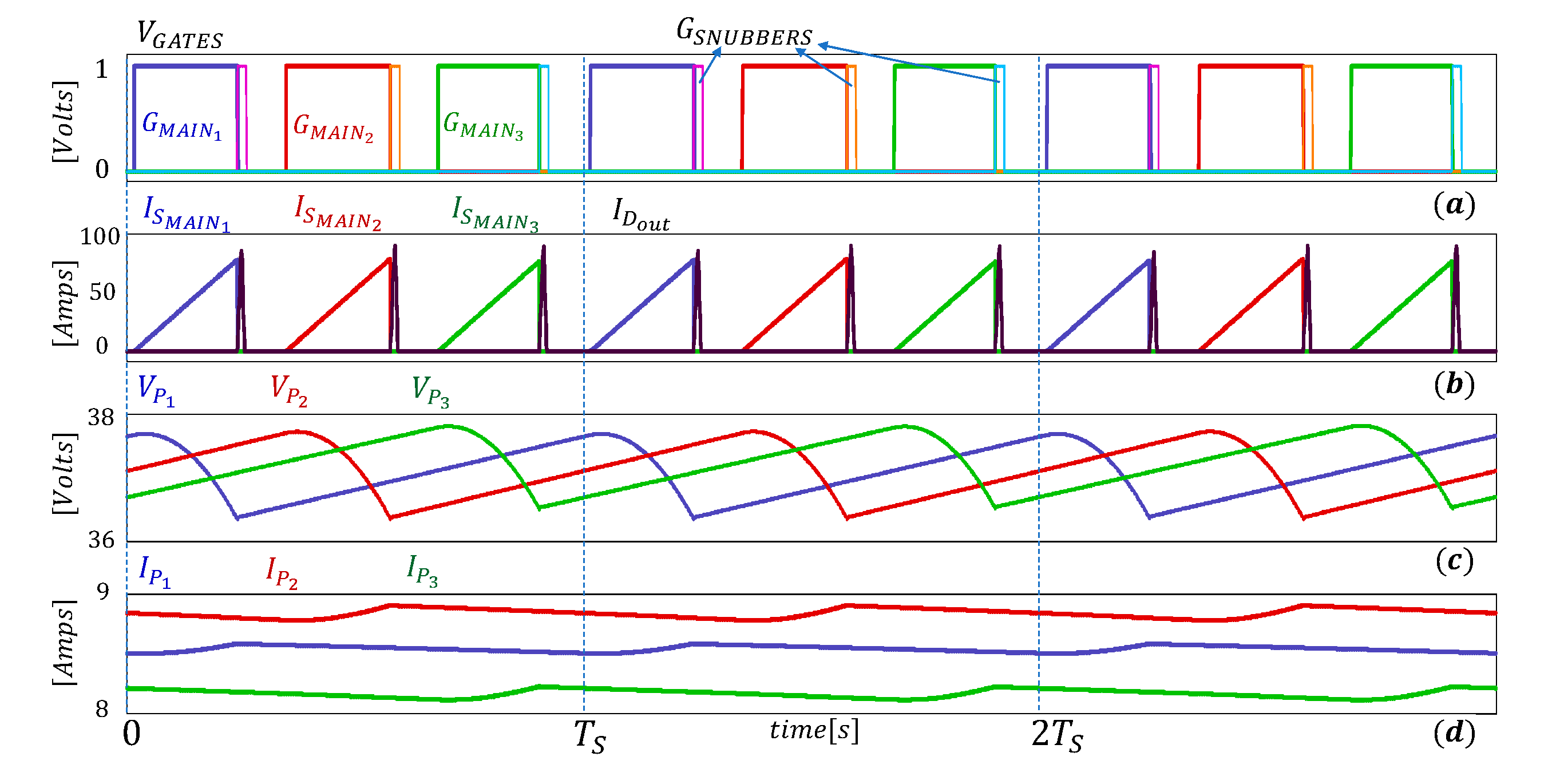
Figure 14 shows four waveforms.
Figure 14a shows the control signals of the main and snubber switches. As can be noted, to protect the devices, there was a dead time between the gating signals of the main and the snubber switches. Active snubbers allowed the drain-source voltages of the main switches not to exceed the allowed ratings and to reduce the
(this is further shown in the experimental results).
Figure 14b shows the currents in the main switches and in the output diode. Slightly different peak values can be appreciated in the three switches currents due to the different solar irradiances.
Figure 14c,d shows the voltages and currents of the solar modules, respectively, where again, different magnitudes can be observed. The performance of the individual MPPT implemented for each PV panel was then verified, considering different irradiance conditions.
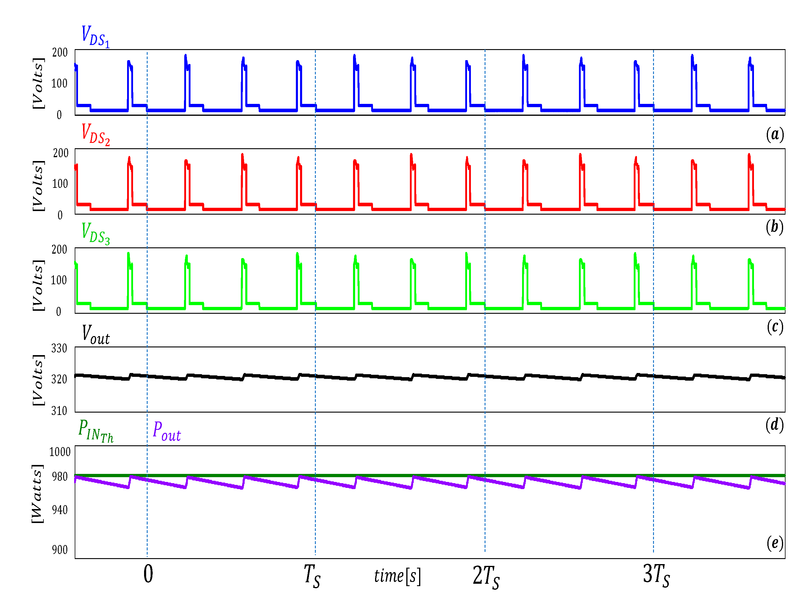
Figure 15 shows five waveforms. The switches voltages are shown in
Figure 15a–c and it can be seen that their magnitudes did not exceed 200 V. In
Figure 15d, the output voltage is depicted, which had an average value of 320 V. Finally,
Figure 15e shows the power in the PV panels (green) and the output power of the proposed converter (blue).
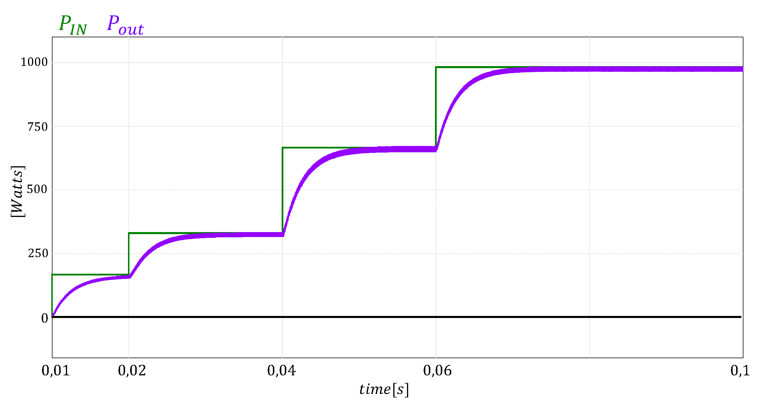
In
Figure 16, the operation of the MPPT can be observed. The power available in the solar panels is shown in green, and the converter output power in purple. Step changes in the solar irradiance were applied. The converter output power closely followed the input available power, validating the correct operation of the MPPT algorithm.
7. Experimental Results
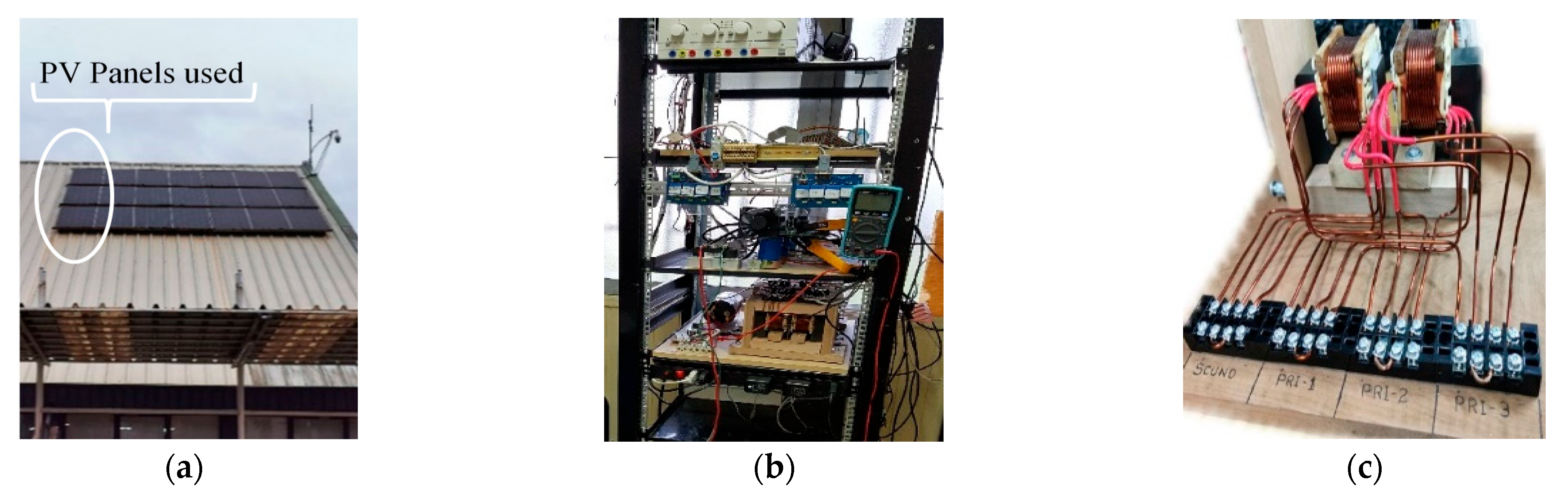
A power converter laboratory prototype was built, and the photovoltaic installation available at the Electrical Engineering Department of the University of La Frontera in Temuco, Chile, was used (see
Figure 17a). In
Figure 17b, the implemented setup for the proposed topology is shown, and in
Figure 17c, the flyback transformer designed and built for the converter is presented. The system parameters are the same as those of the simulations presented in
Table 1. A digital signal processor Texas Instrument F28379D was used as a control platform. Optical fiber was used for the transmission of the semiconductors gating signals. For the main switches, MOSFETs IPW65R041CFD were used, and for the snubber switches, MOSFETs model TK20A60W were considered. The diode model STTH9012TV was used in the converter output. The output capacitor
is in polypropylene to obtain a low series equivalent resistance allowing an increase in the conversion efficiency. The model of the PV panels used was CSUN340-72P, rated at 340 Wp. The experimental system was validated with the same levels of radiation for each PV panel.
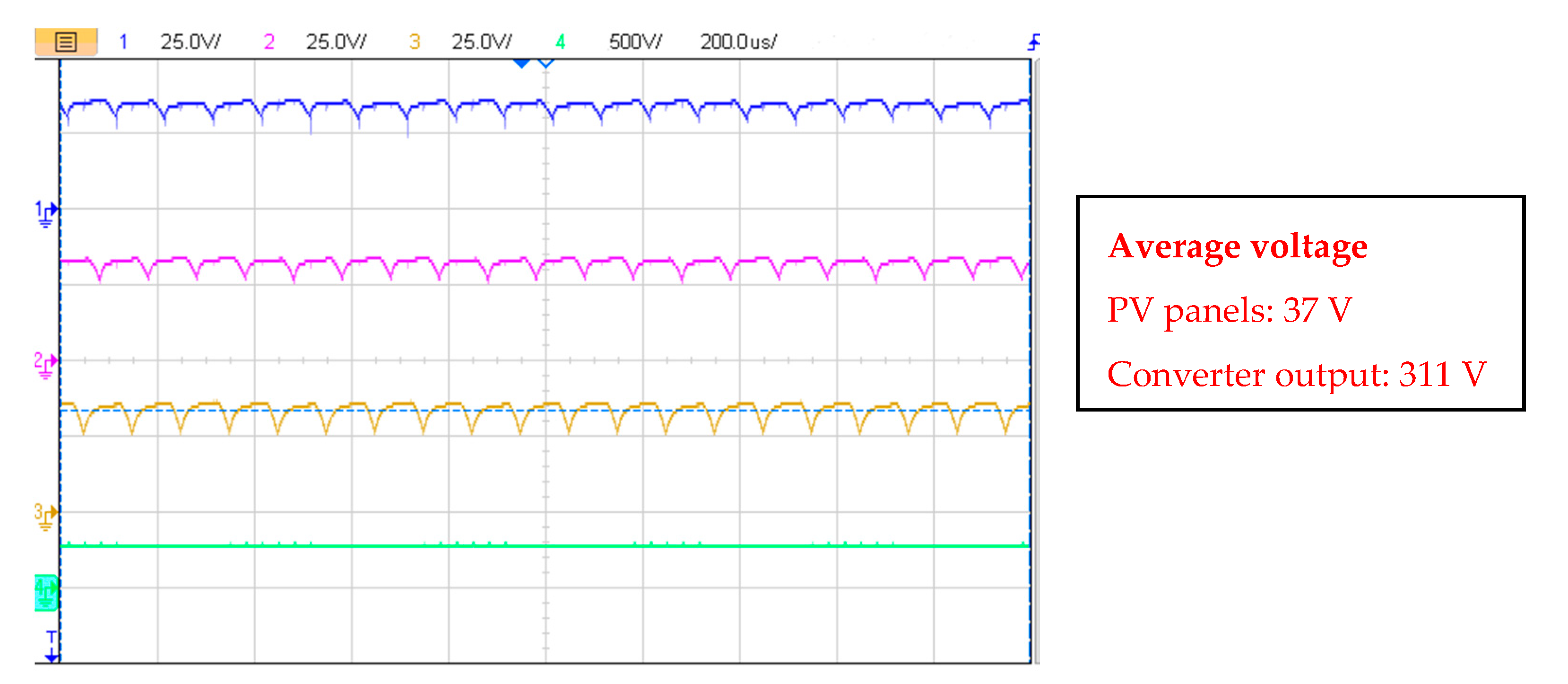
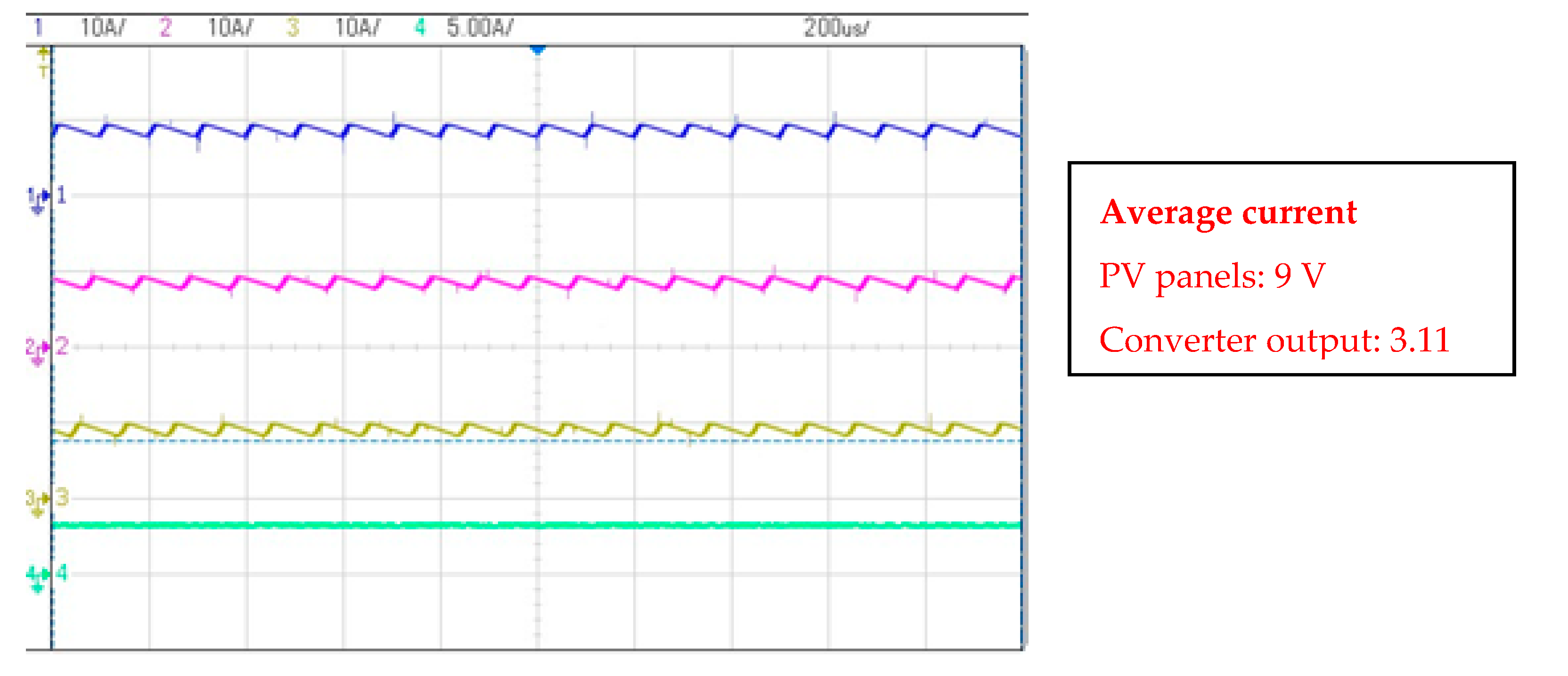
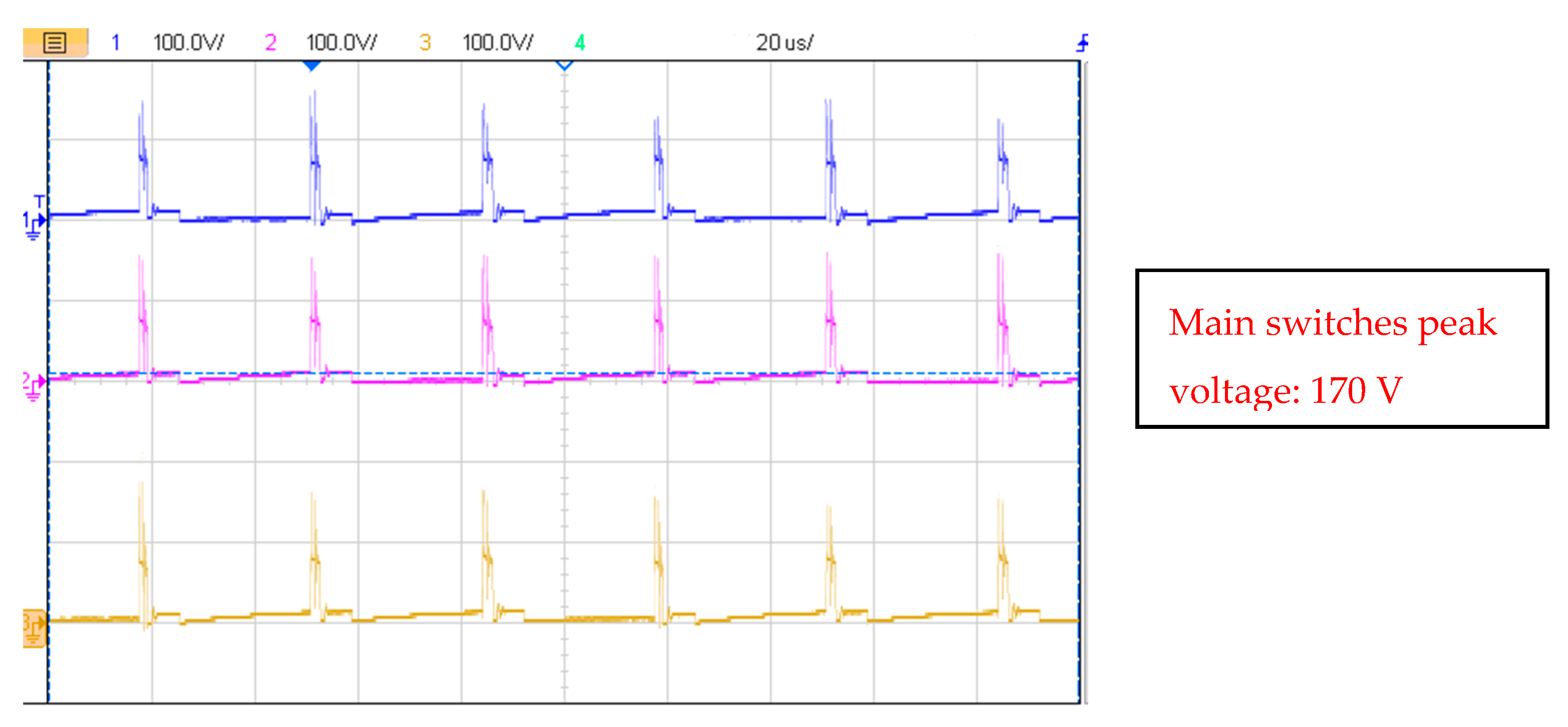
Figure 18,
Figure 19,
Figure 20 and
Figure 21 were obtained around 12 PM.
Figure 18 shows the voltages of the three PV panels and the converter output voltage. It can be noted that the magnitude of the three average voltages was the same (~37 V). The voltage ripple was due to the action of the MPPT control that worked at a frequency of 10kHz. On the other hand, a very low ripple can be observed in the converter output voltage waveform (green) which had an average value of 311 V.
Figure 19 shows the currents of the PV panels (blue, pink, and yellow) and the converter output current (green). The magnitude of the output current was constant and equal to 3.1, while a resistive load of 100 Ω was supplied.
Figure 20 shows the main switches’ voltages. The maximum values did not exceed 170 V. In classical flyback topologies, the energy stored in the transformer leakage inductance produces a
on the main switch; in this work, this problem was solved with the proposed active snubber. This snubber limited the
and injected the energy stored in the transformer’s leakage inductance back to the input capacitor
, increasing the conversion efficiency. The waveforms were similar to the simulated ones shown in
Figure 15.
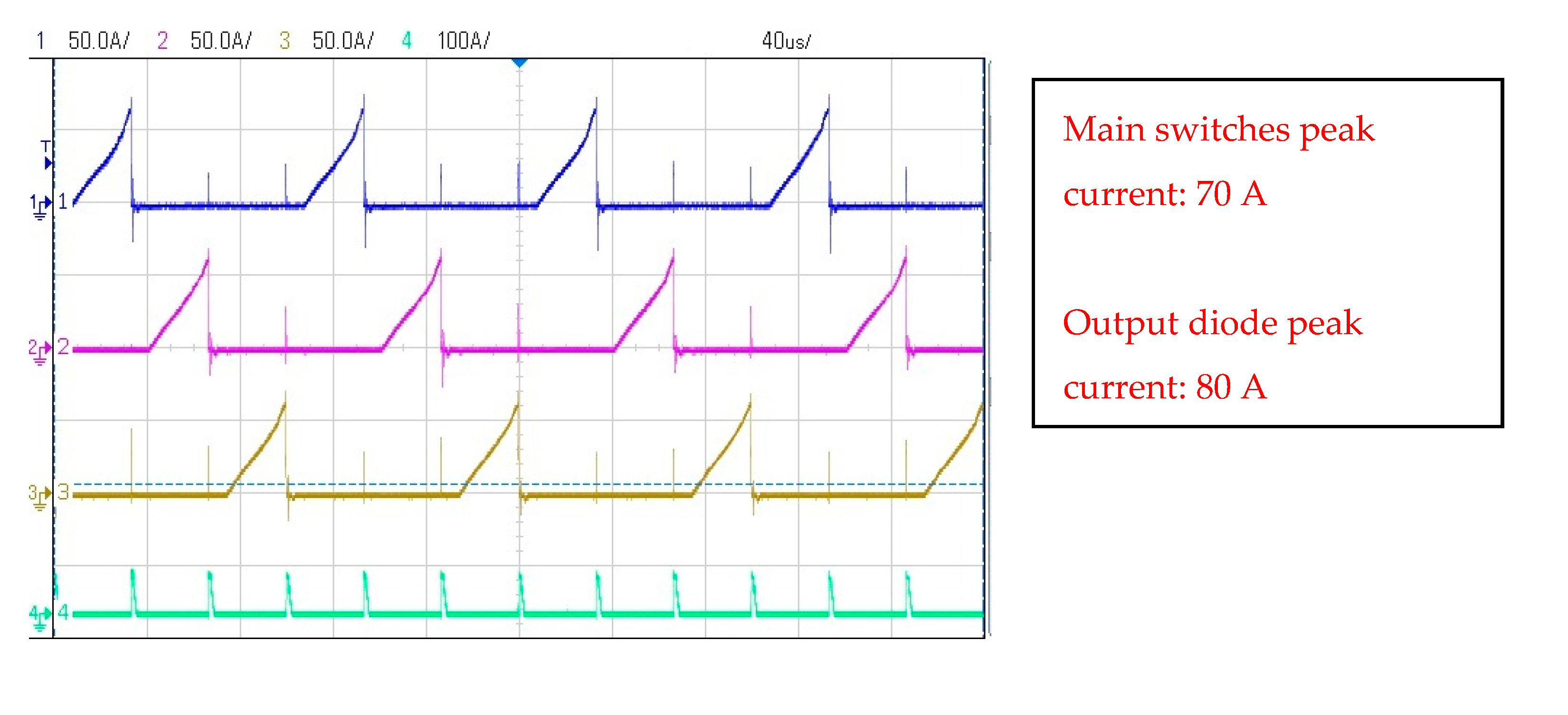
Figure 21 shows the currents on each main switch and the output diode current. The peak current of the main switches was approximately 68 A. For the output diode, the peak current was about 80 A.
The experimental results of
Figure 22 and
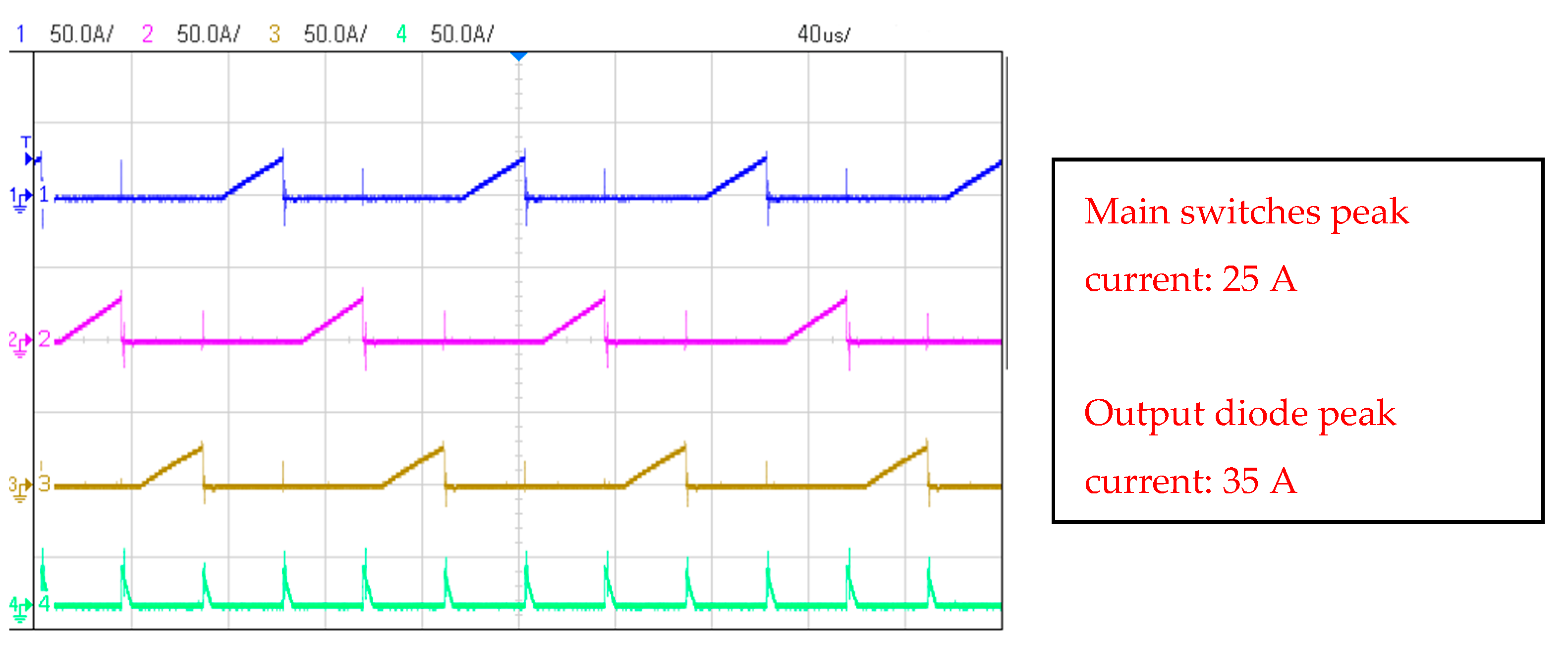
Figure 23 were obtained while operating the converter in the afternoon, close to sunset, when solar irradiation is much lower than at noon. Thus, a reduction in the main switches’ currents and the output diode’s current can be appreciated in
Figure 22. The maximum magnitude of the main switches’ currents was approximately 25 A, and that of the output diode’s was 35 A.
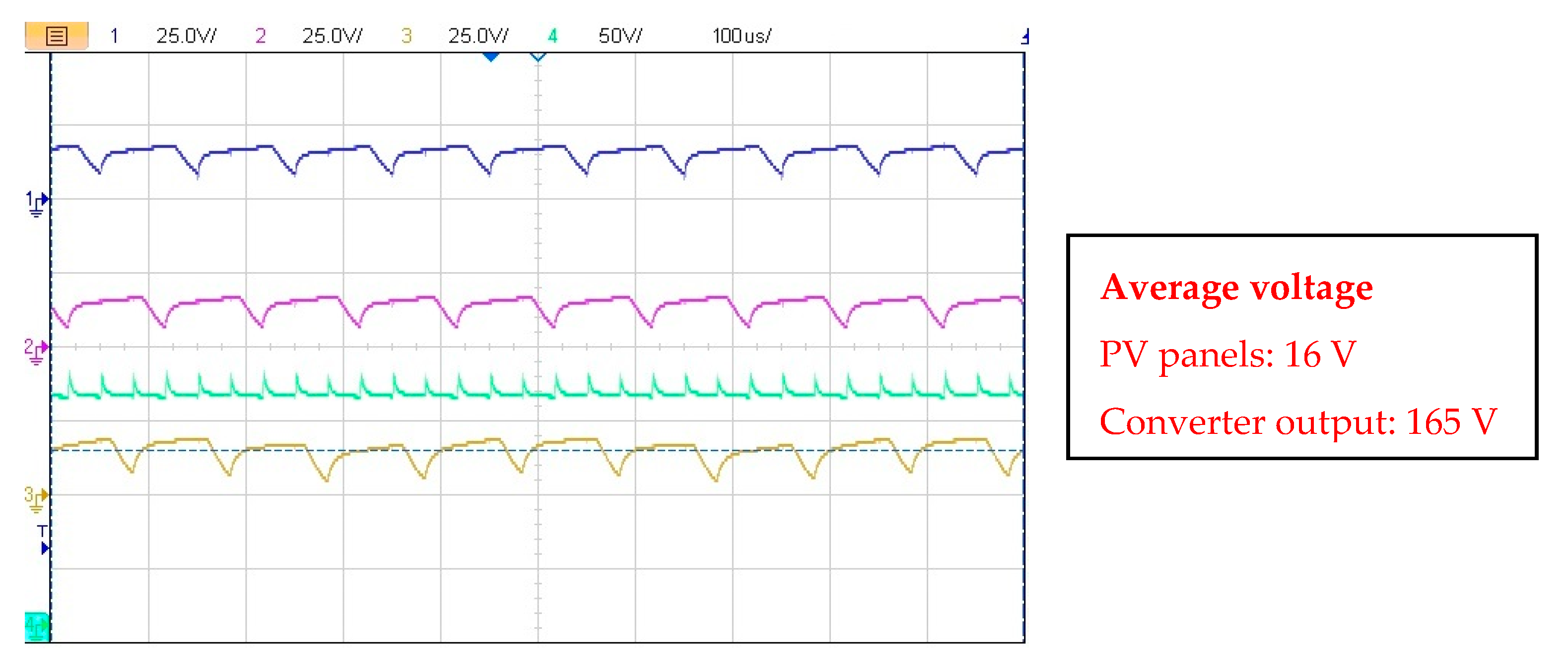
In
Figure 23, the PV panels’ voltages are shown as well as the converter’s output voltage. It can be seen that the voltage of the panels, as well as the converter output voltage are reduced compared to
Figure 17, as a result of the lower solar irradiance. The average voltages of the PVs were 16 V, and the output converter’s average voltage was 165 V.


 ,
, 


