
Highly Sensitive Inertial Micro-Switch for Achieving Adjustable Multi-Threshold Acceleration
1
Key Laboratory of Advanced Manufacturing Technology of the Ministry of Education, Guizhou University, Guiyang 550025, China
2
Mechanical and Aerospace Engineering, University of California, Irvine, CA 92617, USA
3
Chemical and Biomolecular Engineering, University of California, Irvine, CA 92517, USA
4
School of Mechanical Engineering, Dalian University of Technology, Dalian 116023, China
*
Author to whom correspondence should be addressed.
Actuators 2023, 12(2), 53; https://doi.org/10.3390/act12020053
Submission received: 27 December 2022
/
Revised: 18 January 2023
/
Accepted: 23 January 2023
/
Published: 26 January 2023
Abstract
:An inertial micro-switch with multi-threshold acceleration detection capability has been proposed, taking advantage of electromechanical coupling behavior. A mathematical model of electromechanical coupling behavior was established to display the dependence of highly sensitivity on pull-in characteristic and show the ability to detect threshold acceleration by controlling the voltage applied to the inertial micro-switch. The capability of sensitivity and detection that was described in mathematical model was implemented to occur at the inertial switch and showed agreement with that of a simulation. Inertia switches that were comprised of various microstructures with dimensions ranging 3.5 µm from 180 µm were manufactured by means of the micro-electro-mechanical system (MEMS) manufacturing process, and their functions were evaluated by a dropping system. The control method related to the manufacturing of inertial switches was obtained by analyzing the effect of the structural parameters of the inertial switch on threshold voltage and threshold acceleration, resulting in a relatively small error between simulation and experiment. The inertial micro-switch showed high sensitivity to achieving the pull-in effect at 30 V, sense multi-threshold acceleration ranging from 500 g to 2000 g in 2.46 ms and provided enough time for outputting the acceleration signal. Furthermore, the multi-threshold acceleration can be adjusted by controlling the voltage applied to inertial micro-switches. In addition, other functions of inertial micro-switches, such as lower residual stress, high recoverability, and repeatability, have been displayed.
1. Introduction
In the process of miniaturizing and intelligentizing weapons, the attractive merit of the inertial micro-switch derives from high-performance with abundant functionalities [1,2,3,4,5,6,7,8,9,10,11]. The initial feature of the micro-switch allows for low energy consumption, sensing a single acceleration, and providing ON-OFF information in remote areas and hard-to-be-powered applications [7,12,13]. To upgrade the intrinsic performance in the case of conventional inertial micro-switches, the principal philosophy emphasizes quantitative information about the acceleration. In this case, an extraordinary combination of threshold vales and multiple acceleration has been adopted, thus obtaining a threshold-based inertial switch [14]. The threshold-based inertial switches offer several advantages, such as their extraordinary identification of the magnitude of acceleration, and their excellent expansion in the acceleration-detection range [12]. These advantages demonstrate the abundant functionalities of inertial switches for use in various applications [15,16,17,18,19], such as military, automotive, healthcare, and industry, showing more applicability than conventional inertial switches. To further upgrade these advantages, the level of thresholds has been developed for highlighting the advanced nature of inertial micro-switches [12]. Inertial micro-switches with multi-threshold level are promising for enhancing the capability to detect acceleration.
The key feature in the utilization of inertial micro-switches with multi-threshold level in many of the aforementioned applications is the available sensitivity to output signals and detect acceleration. One current method for outputting signals is to enable a lower sensitivity by the use of the flexible fixed electrode for prolonging the contact time and eliminating the rebound during the contact process [20]. However, its contact time of the switch, ranging from 60 μs to 80 μs, is still not enough for processing the signal in an integrated circuit. Although laterally-driven inertial micro-switches, with two L-shaped elastic cantilever beams as the movable electrode [21], have been proposed for prolonging the contact time to 150 μs, its high sensitivity in the contact time is still not conducive to the signal output for a long time. Therefore, a key impediment for inertial micro-switches with multi-threshold level is the challenge of prolonging enough contact time to process signal in an integrated circuit.
Accompanied by an effort to prolong the contact time, the deformation of the movable electrode is prone to occur and inertial switches are only suitable for detecting low acceleration values [22]. In combination with the reduction of the acceleration detection range from 1800 g [12] to 70 g [11], it elaborates that upon prolonging the contact time, the multi-threshold acceleration detection capability has to be weaker and the sensitivity to detect acceleration tends to decrease to a greater extent. Nevertheless, the researchers still tried hard to increase the contact time from 150 μs [21] to 200 μs [23]. The resulting maximum acceleration could not be avoided to decrease from 288 g to 38 g. Obviously, another challenge is to improve the capability of inertial micro-switches to detect threshold acceleration in the condition of prolonging the contact time.
In this paper, the mathematical model of electromechanical coupling behavior is established to demonstrate the pull-in effect and indicate the relationship between the applied voltage and the threshold acceleration. Using the pull-in effect, the self-locking of the inertia switch is proposed to provide a sufficiently long contact time, which is dependent on the power-off time. Using the relationship between the applied voltage and the threshold acceleration, the threshold acceleration ranging from 500 g to 2000 g can be adjusted by altering the applied voltage. Silicon, with large stiffness coefficient, is selected as the material of the movable electrode to improve the recovery ability of deformation and achieve very short response time of inertia, realizing the high sensitivity to detect acceleration. The self-locking function, the adjustable threshold acceleration, and the silicon material of the movable electrode, enable a highly sensitive inertial micro-switch with multi-threshold acceleration detection capability.
2. Modeling and Design
2.1. Mathematical Model and Structural Design
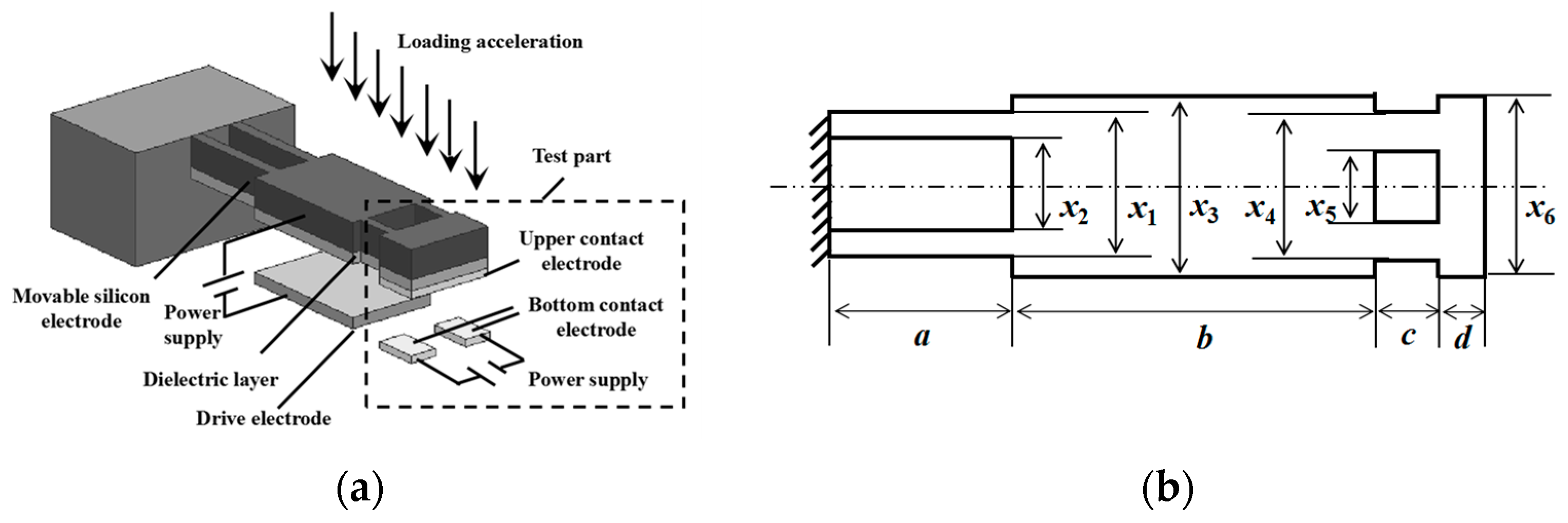
The inertial micro-switch is shown in Figure 1 and consists of five parts as below: silicon-based movable electrode, dielectric layer, upper contact electrode, drive electrode, and bottom contact electrode. Upon applying voltage to the silicon-based movable electrode and the drive electrode, the electrostatic force between them tends to drive the movable electrode to move towards the drive electrode. By increasing the voltage to a critical value, the electrostatic force becomes large enough to overcome elastic force, make the movable electrode bend and deform, and achieve the self-locking function. Meanwhile, the pull-in effect that the upper contact electrode accompanied with movable electrode is quickly adsorbed on the surface of the bottom contact electrode, occurs in the motion process of the movable electrode. As the voltage applied to the movable electrode is below the critical value, the cantilever beam that consists of the silicon-based movable electrode, dielectric layer, and upper contact electrode, is bent to some extent and its upper contact electrode is not adsorbed on the bottom contact electrode. In this case, loading an acceleration onto the bent cantilever beam enables the pull-in effect and the self-locking function, achieving the electromechanical coupling behavior of inertial micro-switch. The threshold value of loading acceleration is adjustable by controlling the voltage to adjust the bending degree of the cantilever beam, which allows the multi-threshold acceleration detection capability of the inertial switch.
Using the calculation method in the MEMS switch integrating actuator and sensor [24], the stiffness coefficient of cantilever beam, which consists of the silicon-based movable electrode, dielectric layer, and upper contact electrode, can be obtained Equation (1) as follows:
where K is stiffness coefficient, E is elastic modulus, h is the thickness of silicon-based movable electrode.
In combination with Equation (1), electrostatic force and elastic force of cantilever beam are respectively shown as below:
where Felec is electrostatic force, m is the mass of cantilever beam, FK is elastic force of cantilever beam, ɛ is dielectric coefficient, A is the area where drive electrode is faced with movable electrode, V is a voltage, y is a displacement of drive electrode, g0 is the gap between dielectric layer and movable electrode.
The static analysis on the pull-in effect is implemented and shows that the condition for achieving the pull-in effect without loading acceleration is that the electrostatic force is equal to the elastic force. In this case, pull-in voltage VP can be calculated by Equation (2):
where y1, y2 and y3 are, respectively, the displacement of movable electrode in the static analysis.
As the kinetic energy theorem and law of conservation of energy are taken into Equation (2), dynamic analysis on the pull-in effect without loading acceleration is performed. Threshold voltage Vthr that is used to achieve the pull-in effect without loading acceleration, can be obtained as follows:
where y5 is the displacement of movable electrode in the dynamic analysis. The values of VP and Vthr, are calculated by the use of MATLAB software, and are optimized by altering the structural parameters of the inertial switch for reducing power consumption. The combination of a sufficiently large stiffness coefficient and a relatively low voltage for achieving high recovery and low power consumption of the inertial switch is used to determine structural parameters as shown in Table 1.
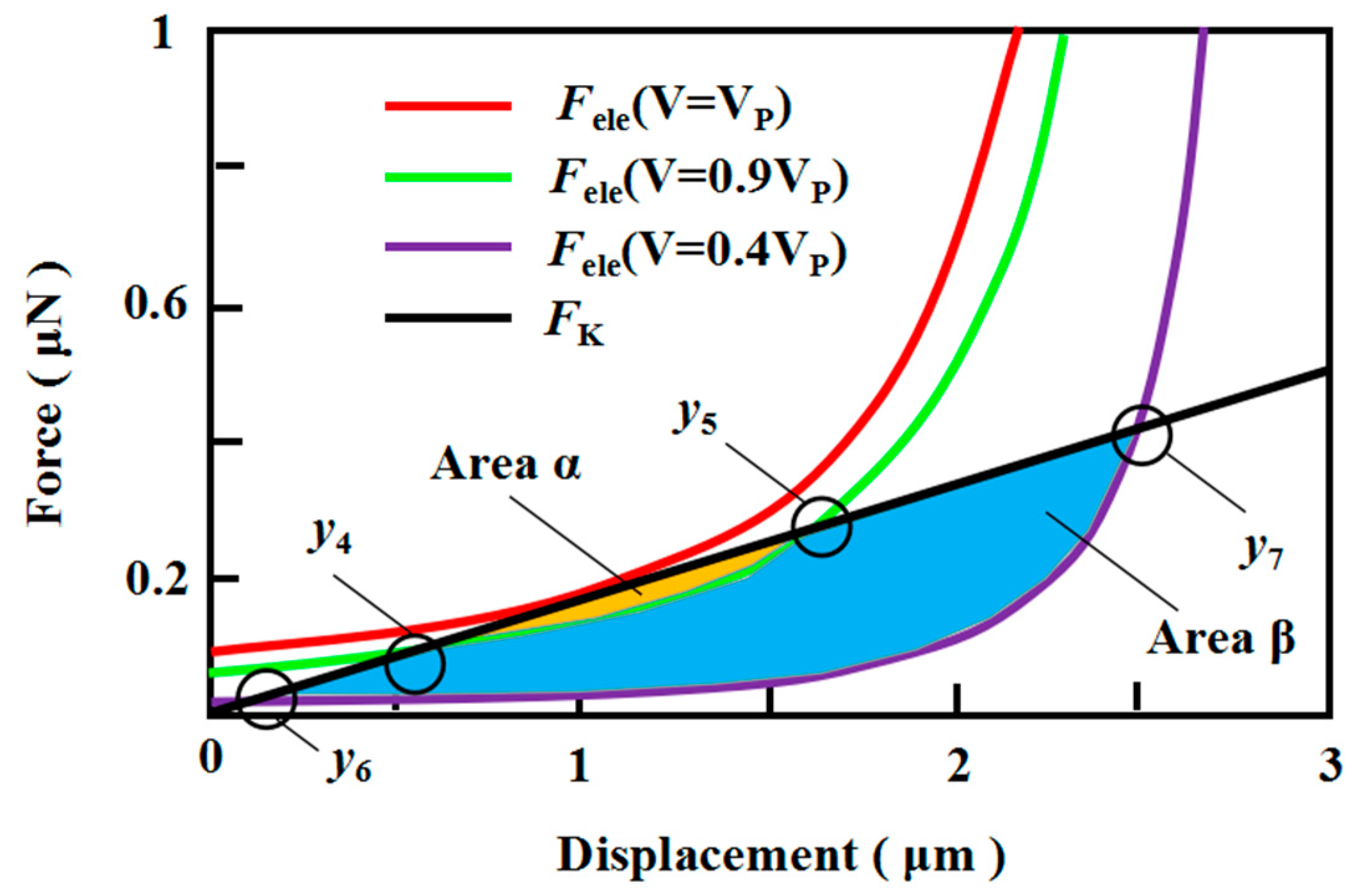
To obtain the threshold acceleration in the electromechanical coupling behavior of the inertial micro-switch, the relationship between Fele and FK is shown in Figure 2, by calculating Equations (1)–(4). The electrostatic force starts to be greater than the elastic force and increases sharply after the cantilever beam reaches y5 or y7, resulting in the self-locking of the inertial switch.
In combination with the law of conservation of energy, the following conditions for realizing the self-locking of a curved cantilever under the action of acceleration, need to be satisfied in Equation (5):
where gthr-1 and gthr-2 are respectively the minimum acceleration at V = 0.9 Vp and V = 0.4 Vp, t0 is loading time of acceleration, and area α and area β are shown in Figure 2.
By substituting the structural parameters of the inertial switch in Table 1 into Equation (5), those threshold acceleration are obtained and are analyzed, showing that the low voltage allows the detection of high acceleration. Further, these pull-in points, such as y5 and y7 in Figure 2, are utilized to achieve fast self-locking of the inertial switch, demonstrating high sensitivity.
2.2. Simulation and Inertial Stress
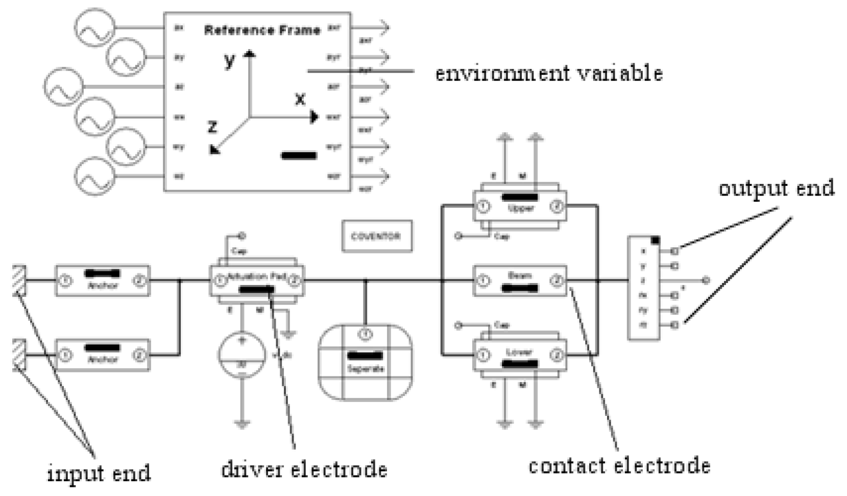
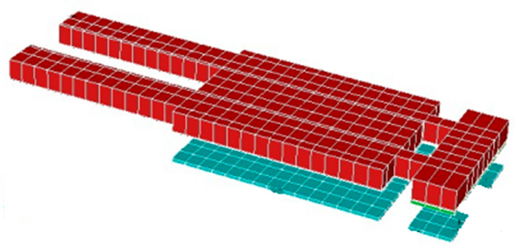
It has already been reported that the system level analysis is faster than the method of the finite element analysis, which results in shortening the design cycle and promoting the further development. Schematic-based system-level modeling is essential to simulate the coupling behavior of inertial micro-switch to the surrounding relevant electronic parts. The main geometric parameters of inertial micro-switch in Table 1 are used to define structural model of inertial micro-switch in system-level modeling, and are substituted into the system-level behavioral model in ConvenorWare. A system-level behavioral model of inertial micro-switch in Figure 3 is established by utilizing the architect platform integrated in CoventorWare, meshing in Figure 4, and setting boundary conditions.
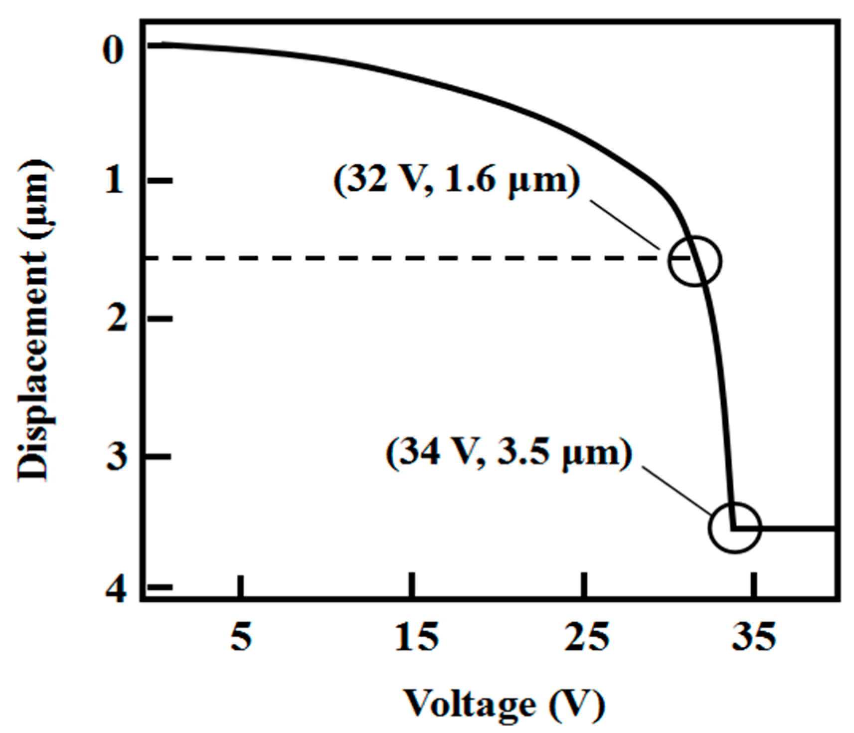
The main geometric parameters in Table 1 are substituted into the above system-level behavioral model in CoventorWare, resulting in the relationship between terminal displacement of micro-switch and driving voltage as shown in Figure 5. As the voltage applied to movable electrode increases from 32 V to 35 V in Figure 5, the displacement of the inertial micro-switch rapidly reaches 3.5 μm and remains constant at 3.5 µm, showing pull-in voltage of 32 V, high sensitivity, and self-locking of the inertial micro-switch. Furthermore, the pull-in voltage and threshold voltages in the mathematical model are calculated by substituting structural parameters into Equations (3) and (4). This comparison based on mathematical model and simulation is carried out in Table 2.
As shown in Table 2, +0.91% is much less than −8.83%, and −26.88% is also smaller than +33.14%, which indicates that Equation (3) is more suitable for static analysis than Equation (4). However, −8.83% shows that the threshold voltage is less than the pull-in voltage, which corresponds to the actual situation. Considering the difference between the pull-in voltage and the threshold voltage in Table 2, Equation (4) is chosen as the control equation for preventing cantilever beam from self-locking in the absence of loading acceleration.
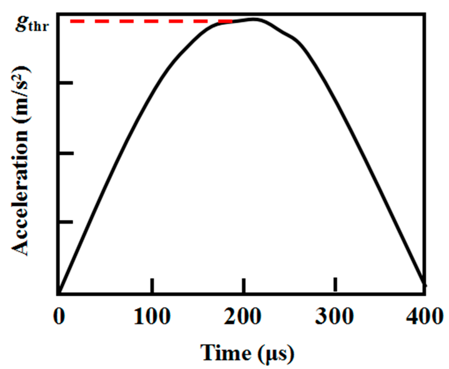
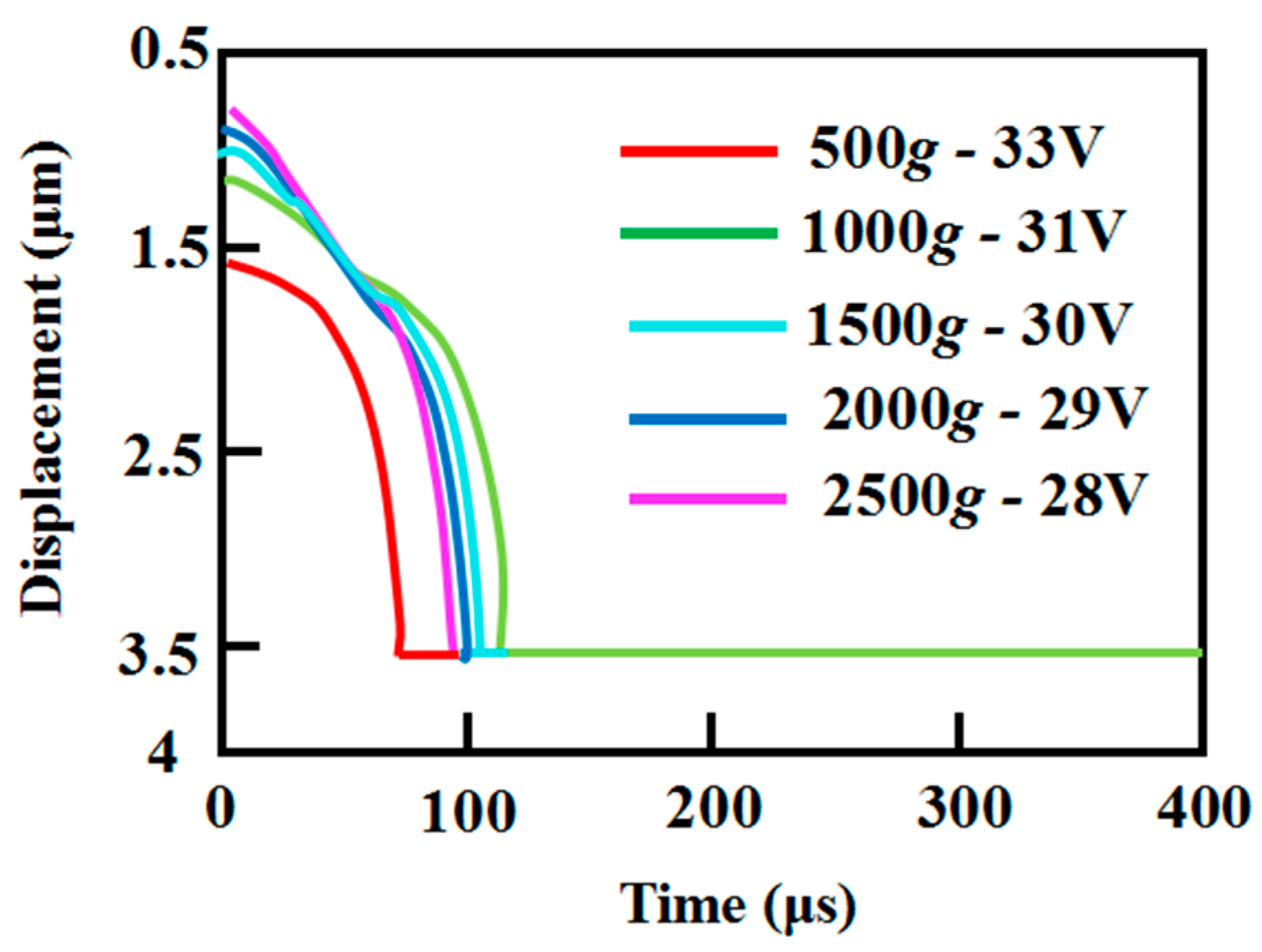
Various voltages lower than the threshold voltage in Equation (4) are respectively applied to the inertial switch, making the cantilever beam bend at different degrees. Using CoventorWare software, electromechanical coupling behavior of inertial switch as is initiated by loading inertial acceleration in Figure 6 onto the bent cantilever beam and shown in Figure 7. The relationship between loading acceleration gthr and voltage in Figure 7 corresponds to the electromechanical coupling behavior of inertial switch, showing the ability to obtain multi-threshold acceleration ranging from 500 g to 2500 g by adjusting voltage. Moreover, accelerating movement in the process of reducing displacement to 3.5 µm in Figure 7, demonstrates the pull-in effect and the high sensitivity. Upon reaching the 3.5 µm position, there is no further change in the movement displacement, which realizes the self-locking of inertial micro-switch.
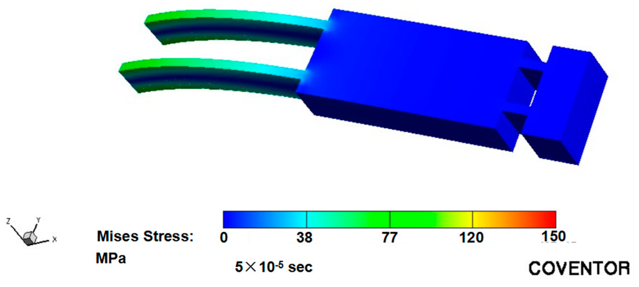
The reliability required for detecting acceleration needs to be taken into account. Using Coventor software, the stress distribution in Figure 8 can be displayed under half-sine acceleration of 800 μs and 10,000× g. Then the allowable stress of material is equal to
In this equation, the value of n ranges from 4 to 5. The value of σp in Equation (6) is
In Equations (6) and (7), [σ] is the allowable stress of the material, n is the security coefficient, and σp is the limit strength.
By substituting Equation (7) into Equation (6), the value of [σ] is obtained and ranges from 334 MPa to 417.5 MPa. The maximum inertial stress seen from Figure 8 is 150 MPa and is less than the value of [σ], which enables that plastic deformation and fracture will not occur.
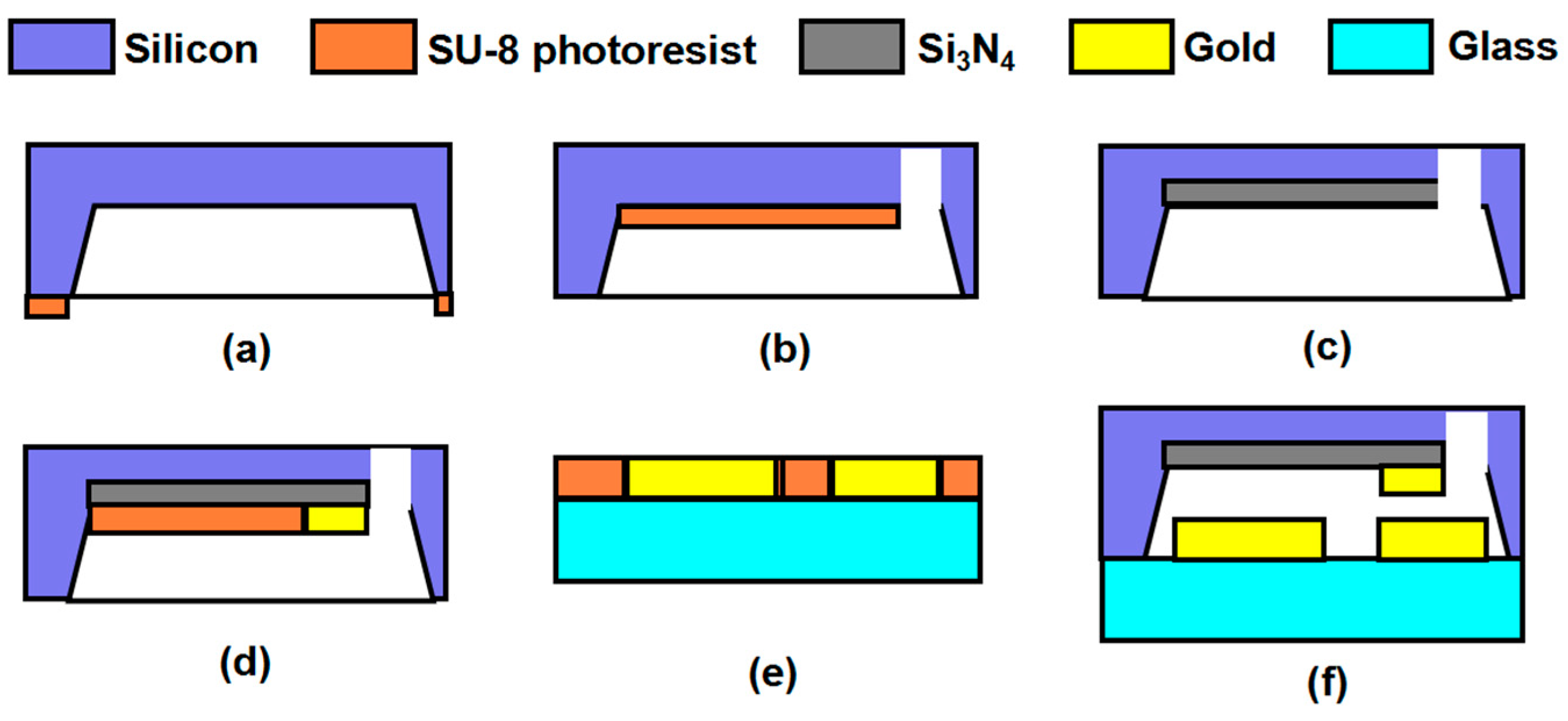
3. Micro-Fabrication of Inertial Micro-Switch
Inertial micro-switches are fabricated in accordance with the fabrication flow in Figure 9 in the super clean room. In the manufacturing process, the etching is performed, and the materials of inertial micro-switches in Table 1 and the packaging step in Figure 9, are displayed as follows:
(a) Substrate. Pyrex and borofloat glass are ideally suited as substrate owing to high resistivity (the order of 1010 Ωcm), high inertness to most acids and other chemicals, and small thermal coefficient of expansion (TCE) [25]. By bonding with metals, they are selected to package MEMS devices, achieving the integration of mechanical and electrical components. Deep reactive ionic etch is processed by the use of a patterned SU-8 photoresist layer, resulting in the structures in Figure 9a,b.
(b) Contact electrode. Gold offers several advantages such as, high conductivity and chemically inertness, allowing to reduce the losses and to prevent contamination and corrosion [26].
(c) Movable electrode. Properties such as yield, creep and thermal relaxation need to be taken into account for accommodating the bending of the movable electrode and its recovery from deformation. In addition to the excellence in these properties, polysilicon also exhibits non-homogeneities in the stress distribution. In combination with the dependence of the MEMS manufacturing process on polysilicon, polysilicon is chosen as the material of movable electrodes.
(d) Dielectric layer. Before actuation (E < 1 MV/cm), the current through the dielectric Si3N4 layer increases approximately linearly with field [27], which offers the possibility to improve the uniformity of the electrostatic field between movable electrode and contact electrode. In the combination of lower conductivity, Si3N4 is often chosen as the material of the dielectric layer to avoid short circuits. The SU-8 photoresist layer in Figure 9b is removed by the use of developer, and Si3N4 is deposited at the side in Figure 9c by using a low-pressure chemical vapor deposition, ultimately forming dielectric layer-Si3N4 layer.
(e) Packaging. The interference derived from electromagnetic wave in the process of detecting acceleration need to be shielded for outputting the acceleration signal. To avoid the interference, the inertial micro-switch including movable electrode, drive electrode, upper contact electrode, dielectric layer and bottom contact electrode, is encapsulated by the use of tubular metal case. SU-8 photoresist layers in Figure 9d,e are removed by the use of developer, and then an aligned anodic bonding between structures in Figure 9d,e is implemented at a temperature of 300 °C, chamber pressure of 1 Pa, and bonding voltage of 900 V. The resulting structure of the inertial micro-switch is obtained and shown in Figure 9f.
4. Testing and Discussion
4.1. Threshold Voltage of Inertial Micro-Switch
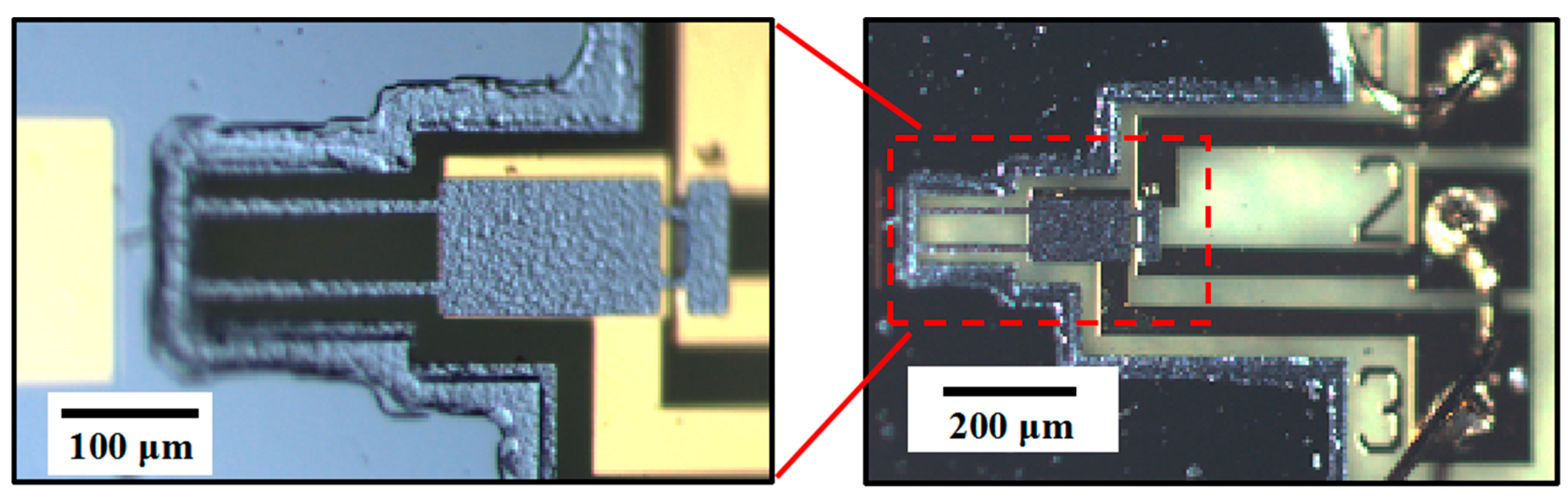
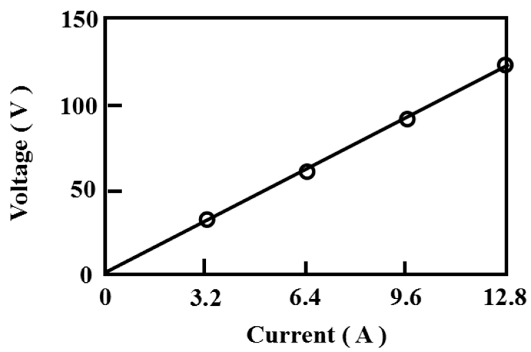
Based on the above MEMS manufacturing process, the inertial switch shown in Figure 10 is obtained. Structural parameters in inertial switch are measured by optical microscope, and are shown as below: a = 180.2 µm, b = 160.68 µm, x1 = 72 µm, x2 = 49.38 µm, x3 = 104.3 µm, h = 6.896 µm, and g0 = 3.084 µm. Power supply is connected with the movable electrode and the drive electrode in the inertial micro-switch for supplying voltage. Meanwhile, metatable Keithley (2036B) is selected to measure the output signal that derives from the current between upper contact electrode and bottom contact electrode. By controlling power supply, the voltage between the movable electrode and the drive electrode gradually increases from 0 V to 35 V. The current–voltage curve obtained by metatable Keithley (2036B) is shown in Figure 11 when the voltage is equal to or much more than 30 V. The resistance of 9.6 Ω between upper contact electrode and bottom contact electrode is calculated based on the slope of the current–voltage curve in Figure 11. Relative error of 16.7% between the measurement value and the design value of resistance is obtained, showing that the current-voltage curve derives from the contacting between upper contact electrode and bottom contact electrode. The dependence of the current–voltage curve on threshold voltage demonstrates 30 V is the threshold voltage of inertial micro-switch.
To show the effect of the mathematical model on the experimental threshold voltage, structural parameters measured in Figure 10 are respectively substituted into Equations (3) and (4), and the relative errors between those voltages and experimental value (30 V) can be easily obtained in Table 3. 13.6% and +7.63% in Table 3 are greater than 4.37%, demonstrating that the actuation voltage of 30 V is threshold voltage but not pull-in voltage. In addition, 1.1% means the progressiveness and superiority of mathematical model and manufacturing technology.
For controlling threshold voltage, the analysis of errors needs to be taken into consideration. As structural parameters measured in Figure 10 are respectively taken into Equation (4), the errors between the corresponding threshold voltage and 31.31 V can be obtained in Table 4.
Processing errors ranging from −10.62 µm to +6.4 µm in Table 4 are relatively small, which reflects the excellence of the MEMS machining process. For the same processing errors, errors of h and g0 are as shown in Table 4, easily affect the magnitude of threshold voltage, and need to be strictly controlled. The combination of positive deviation in h and negative deviation in x2, explains the reason that 31.31 V is greater than 29.67 V. By analyzing the effect of processing errors on threshold voltage in Table 4, the compensation method for controlling threshold voltage has been proposed by decreasing the values of x1, x2 and g0, and increasing the value of h for achieving smaller relative error between the experimental value and design value of threshold voltage.
A stress gradient in the normal direction of fixed–fixed beams or cantilever beams often occur in their multi-layer structures owing to the stress difference in the components of multi-layer structures (Si3N4/Au) [27]. In the case of an inertial micro-switch, the stress difference between movable electrode and dielectric layer can be calculated as follows:
with .
Where σ1 and σ2 are respectively the residual stresses of movable electrode and dielectric layer, h and t1 are respectively the thicknesses of movable electrode and dielectric layer, Δz is a deflection at the tip of two-layer beam, Ee is equivalent to Young’ modulus of inertial micro-switch, E1 and E2 are respectively the Young’ modulus of movable electrode and dielectric layer.
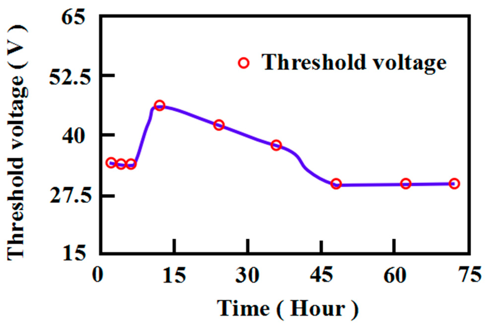
By substituting threshold voltage of 34 V and 30 V into Equation (3), Δz = 0.19 µm can easily be obtained. In combination with structural parameters of the Si–Si3N4 cantilever beam, such as, h = 6.896 µm, t1 = 0.728 µm, L = 393.98 µm, Ee = 172.3 GPa, the value of Δσ in Equation (8) is calculated out and is equal to 6.2 MPa, which is acceptable in the stress difference of less than 5 MPa for designing MEMS switch [28]. The residual stress of the cantilever beam in the inertial micro-switch is evaluated by prolonging the time in the process of applying threshold voltage, as shown in Figure 12. Most of the threshold voltages are concentrated around 32 V at the loading time from 1 h to 74 h, demonstrating the relative errors—+8.59% and −4.18%, and the low residual stress of the inertial switch.
4.2. Multi-Threshold Acceleration of Inertial Micro-Switch
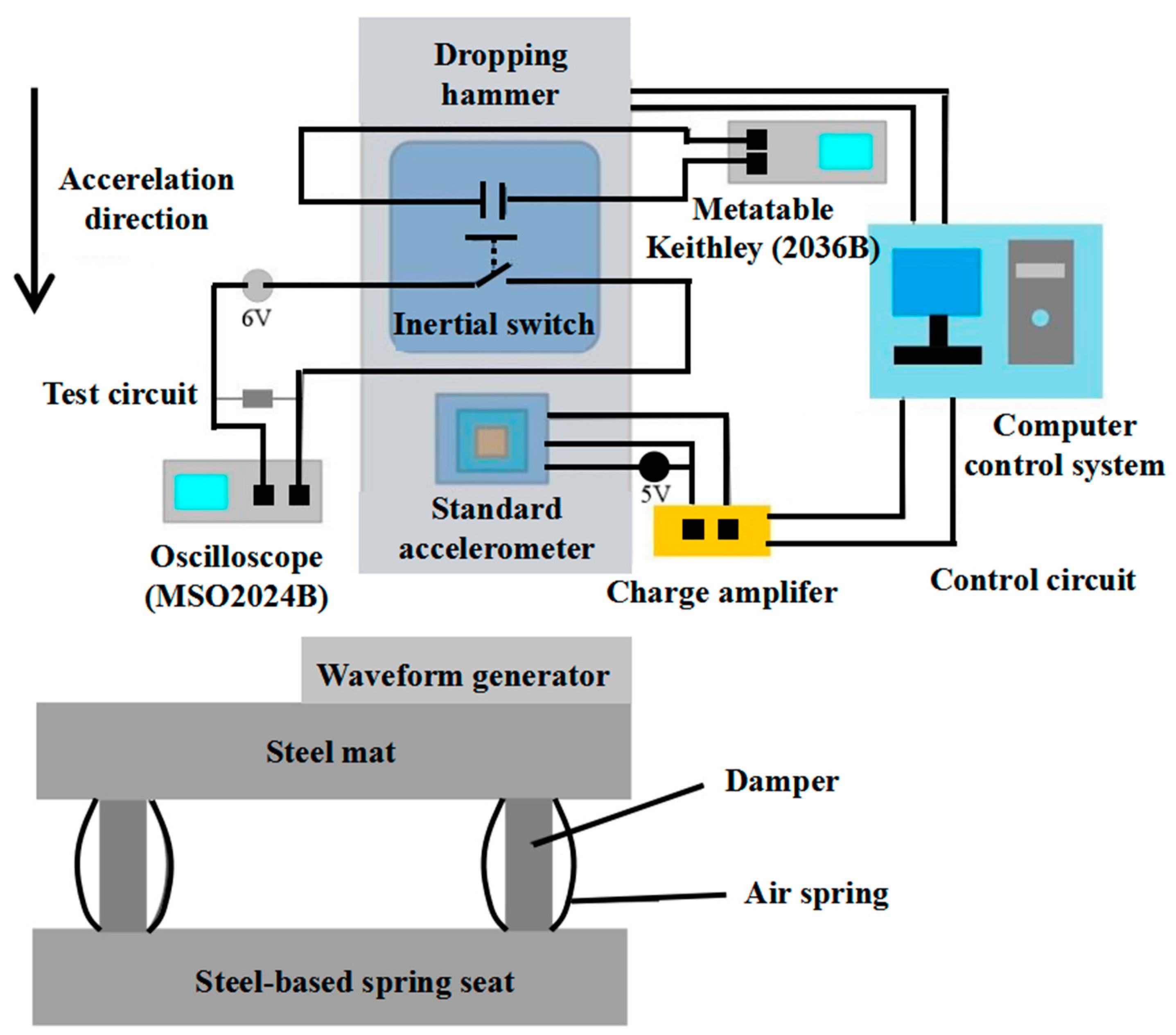
To detect multi-threshold acceleration, a dropping system is established in Figure 13, and consists of a dropping hammer, metatable measurement device (Keithley 2036B), standard accelerometer (DL112), oscilloscope (Tektronix MSO2024B), et al. A standard accelerometer is used to test threshold acceleration gthr that is applied to inertial micro-switch by dropping system. Oscilloscope is selected to collect the output signal of inertial micro-switch. The packaged switch and the standard accelerometer are both fixed at the top of a steel dropping platform. As the dropping hammer moves to hit the waveform generator, the inertial micro-switch is dropped freely from a pre-set height, generating half-sine wave acceleration under the action of damper and air spring.
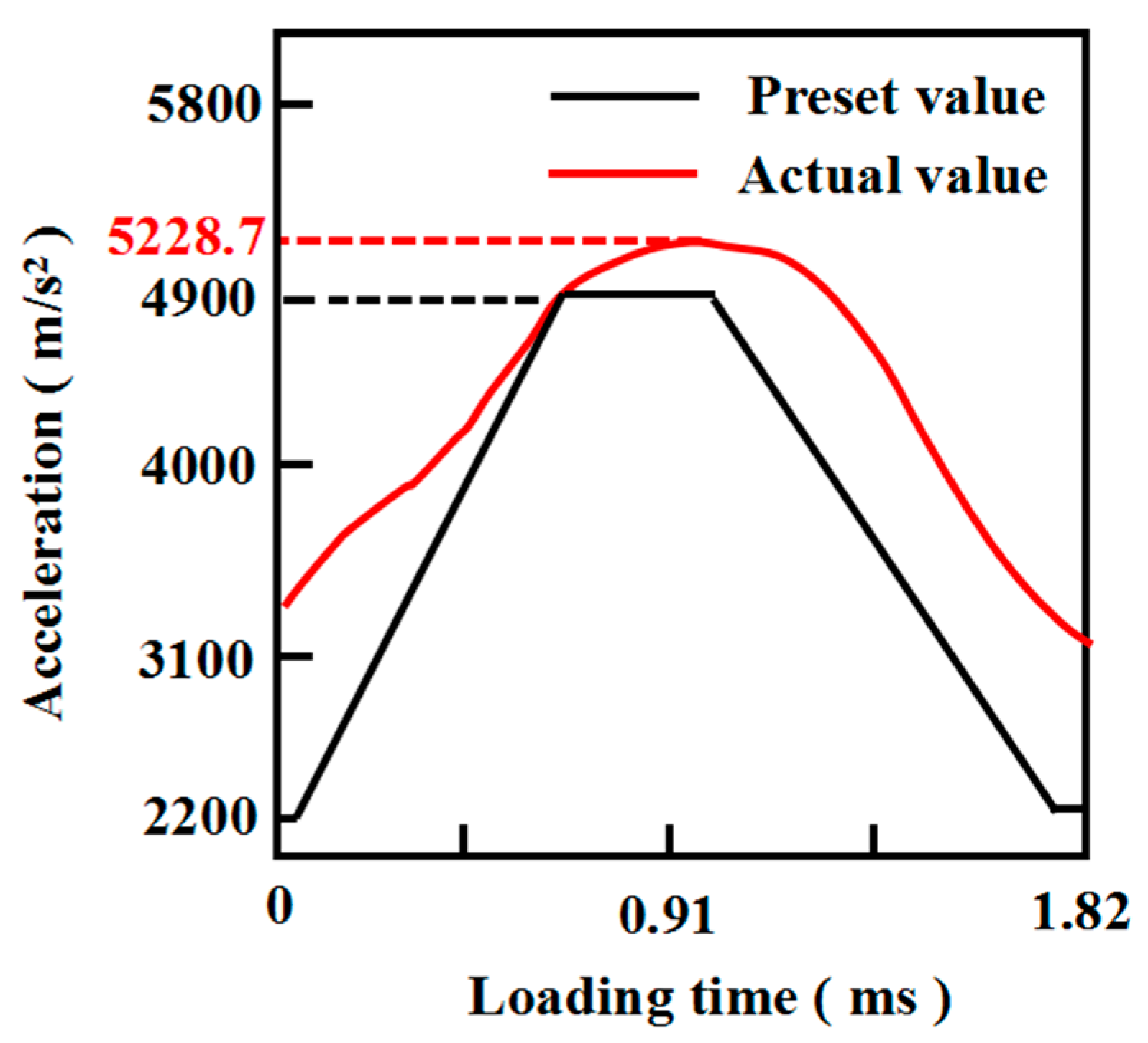
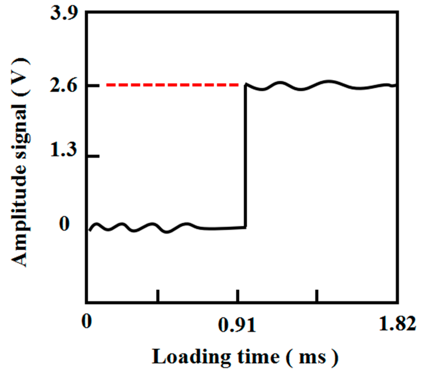
Using the dropping system in Figure 13, the preset value of 4900 m/s2 inertial acceleration at time of 1.82 ms in Figure 14, is loaded to the inertial micro-switch that the voltage of 25 V has been applied to. In the loading process, the actual value of inertial acceleration (5228.7 m/s2) in Figure 14 is tested by the standard accelerometer. The step (2.6 V) of the amplitude signal in oscilloscope in Figure 15 exhibits the generation of the signal, indicating the pull-in effect between cantilever beam and bottom contact electrode in the inertial micro-switch. The relatively small fluctuations exhibited after a step of 2.6 V in the amplitude signal show the ability to resist electromagnetic interference. In electromechanical coupling behavior, the acceleration detected in experiments have a deviation of +6.71% from that in simulation, as shown in Table 5. The error of +6.71%, that is less than 10%, can be achieved by increasing the loading time from 0.4 ms to 1.82 ms and reducing the voltage from 33 V to 25 V, thus making a high detection capability.
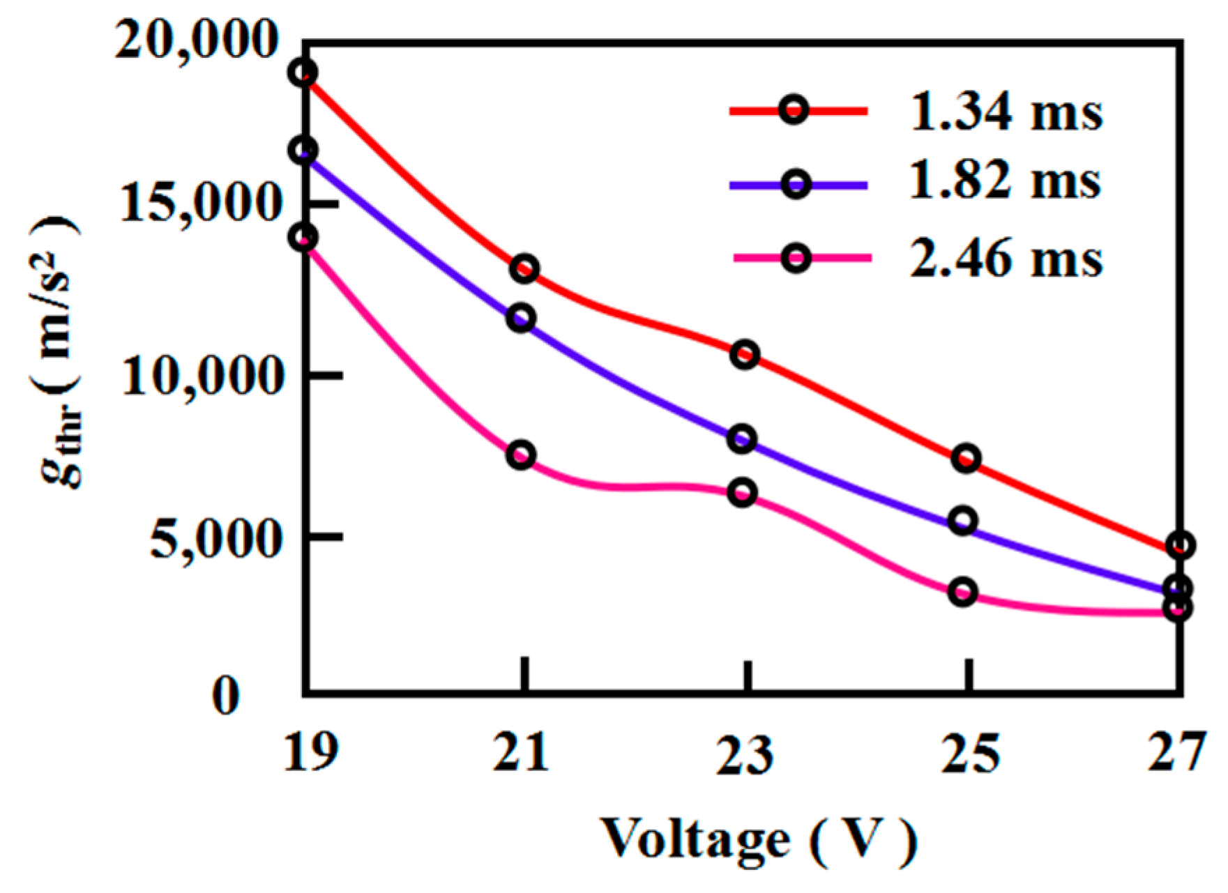
To demonstrate electromechanical coupling behavior, correspondence between acceleration and voltage in the pull-in effect is obtained in Figure 16. Upon applying the voltage ranging from 19 V to 27 V to inertial micro-switch, the corresponding acceleration that varies from 500 g (5000 m/s2) to 2000 g (20,000 m/s2) needs to be loaded for achieving the pull-in effect and is only one at the specified time, showing the ability to detect multi-threshold acceleration. Further investigation into the effect of threshold acceleration on voltage reveals a decreasing linear trend of threshold acceleration versus voltage as shown in Figure 16, which coincides with that in simulation. In the case of constant threshold acceleration, the higher loading time in Figure 16 ensures the pull-in effect of the inertial micro-switch at a low voltage, explaining the reason for having a relatively low error of 6.71% in Table 5. The inertial switch is able to respond to acceleration and output a voltage signal within the loading time varied from 1.34 ms to 2.46 ms, showing high sensitivity of the inertial micro-switch.
Inertial switches with various characteristic dimensions and materials are fabricated for investigating their characteristics, as shown in Table 6. The lower threshold voltage of 30 V and the lowest functional consumption of 1.087N·µm in Table 6 demonstrate the superiority of inertial switches as electronic devices. The recovery time of 1 min in the coupling behaviors shows the ability to resist the deformation of inertial micro-switch, demonstrating higher recoverability. The coupling behavior can be repeated up to 260 times, showing high repeatability. These excellent features demonstrate the advancement for selecting the materials of movable electrode and dielectric layer, and designing the structures of inertial switch in this paper. It is believed that highly sensitive inertial micro-switch with multi-threshold acceleration detection capability is able to overcome the severely damage derived from a mechanical impact and/or an electrical arcing in the solid–solid contact in typical micro-switches [29,30]. Moreover, the detection range of threshold acceleration from 500 g to 2000 g in 2.46 ms almost exceeds that of existing switches [2,11,20,21,31,32,33], demonstrating the high sensitivity of the inertial switches in this paper.
5. Conclusions
A mathematical model of electromechanical coupling behavior is developed to clarify that it is feasible to assign multi-threshold acceleration to an inertial switch by regulating the bending degree of its cantilever beam, which can be controlled by voltage between movable electrode and drive electrode. Simulation of electromechanical coupling behavior is implemented to show that the analysis of the mathematical model is reasonable. Inertial micro-switches are fabricated by means of MEMS manufacturing process and are tested with the use of a dropping system. The compensation method for controlling threshold voltage has been proposed to achieve smaller relative error between the experimental value and design value of threshold voltage. The inertial micro-switch shows high sensitivity to detect multi-threshold acceleration and provides more than enough time for the output signal. Lower residual stress, high recoverability, and repeatability, present the advanced nature of inertial switches.
Author Contributions
Conceptualization, J.D.; methodology, J.D. and D.S.; software, J.D., D.S. and S.S.; validation, J.D., D.S. and S.S.; formal analysis, J.D., D.S. and S.S.; investigation, J.D., D.S. and S.S.; resources, J.D., D.S. and S.S.; writing—original draft preparation, J.D.; writing—review and editing, J.D., D.S. and S.S.; visualization, J.D., D.S. and S.S.; supervision, J.D.; project administration, J.D.; funding acquisition, J.D. All authors have read and agreed to the published version of the manuscript.
Funding
This work is partly supported by the the Science and Technology Foundation of Guizhou Province under grant PTRC[2020]6007.
Institutional Review Board Statement
Not applicable.
Informed Consent Statement
Not applicable.
Data Availability Statement
The data that support the findings of this study are available from the corresponding author upon reasonable request.
Conflicts of Interest
The authors declare no conflict of interest.
References
- Ren, C.; Wang, K.; Zhang, P.; Li, Y.; Zhao, Z.; Shi, X.; Yang, Z. A Self-Powered MEMS Inertial Switch for Potential Zero Power-Consumption Wake-Up Application. J. Microelectromech. Syst. 2021, 30, 550–559. [Google Scholar] [CrossRef]
- Lee, I.J.; Song, Y.; Jung, H.; Choi, J.; Eun, Y. Deformable carbon nanotube-contact pads for inertial microswitch to extend contact time. IEEE Trans. Ind. Electron. 2011, 59, 4914–4920. [Google Scholar] [CrossRef]
- Currano, L.J.; Becker, C.; Smith, G.; Isaacson, B.; Morris, C.J. 3-axis acceleration switch for traumatic brain injury early warning. In Proceedings of the 2012 IEEE 25th International Conference on Micro Electro Mechanical Systems (MEMS), Paris, France, 29 January–2 February 2012; pp. 484–487. [Google Scholar]
- Xu, Q.; Yang, Z.; Sun, Y.; Lai, L.; Jin, Z.; Ding, G.; Zhao, X.; Yao, J.; Wang, J. Shock-resistibility of mems-based inertial microswitch under reverse directional ultra-high g acceleration for IoT applications. Sci. Rep. 2017, 7, 45512. [Google Scholar] [CrossRef] [PubMed] [Green Version]
- Cao, Y.; Xi, Z.; Yu, P.; Wang, J.; Nie, W. Optical measurement of the dynamic contact process of a MEMS inertial switch under high shock loads. IEEE Trans. Ind. Electron. 2016, 64, 701–709. [Google Scholar] [CrossRef]
- Liu, M.; Zhu, Y.; Wang, C.; Chen, Y.; Wu, Y.; Zhang, H.; Wang, W. A novel low-g MEMS bistable inertial switch with self-locking and reverse-unlocking functions. J. Microelectromech. Syst. 2020, 29, 1493–1503. [Google Scholar] [CrossRef]
- Michaelis, S.; Timme, H.; Wycisk, M.; Binder, J. Additive electroplating technology as a post-CMOS process for the production of MEMS acceleration-threshold switches for transportation applications. J. Micromech. Microeng. 2000, 10, 120–123. [Google Scholar] [CrossRef]
- Li, Y.; Zhao, J.; Wang, W.; Zhao, W.; Zhao, W.; Zhu, H. A low-g MEMS inertial switch with a novel radial electrode for uniform omnidirectional sensitivity. Sens. Actuators A Phys. 2018, 270, 214–222. [Google Scholar]
- Zhang, X.; Xiang, X.; Wang, Y.; Ding, G.; Xu, X.; Yang, Z. A Heterogeneous Integrated MEMS Inertial Switch with Compliant Cantilevers Fixed Electrode and Electrostatic Locking to Realize Stable On-State. J. Microelectromech. Syst. 2019, 28, 977–986. [Google Scholar] [CrossRef]
- Ouakad, H.; Younis, M.; Alsaleem, F. Dynamic response of an electrostatically actuated microbeam to drop-table test. J. Micromech. Microeng. 2012, 22, 095003. [Google Scholar] [CrossRef]
- Zhang, P.; Li, Y.; Ren, C.; Zhang, H.; Shi, X.; Liu, Y.; Yang, Z. A MEMS Inertial Switch With Large Scale Bi-Directional Adjustable Threshold Function. J. Microelectromech Syst. 2021, 31, 124–133. [Google Scholar] [CrossRef]
- Xu, Q.; Khan, F.; Younis, M.I. Multi-Threshold Inertial Switch for Quantitative Acceleration Measurements. IEEE Sens. J. 2021, 21, 23849–23859. [Google Scholar] [CrossRef]
- Cai, H.G.; Yang, Z.; Ding, G.; Wang, H. Development of a novel MEMS inertial switch with a compliant stationary electrode. IEEE Sensors J. 2009, 9, 801–808. [Google Scholar] [CrossRef]
- Xu, Q.; Wang, L.; Younis, M.I. Multi-threshold Inertial Switch with Acceleration Direction Detection Capability. IEEE Trans. Ind. Electron. 2022, 70, 4226–4235. [Google Scholar] [CrossRef]
- Xi, Z.; Kong, N.; Nie, W.; Cao, Y.; Zheng, C. High g MEMS inertial switch capable of direction detection. Sens. Actuators A Phys. 2019, 296, 7–16. [Google Scholar] [CrossRef]
- Post, A.; Hoshizaki, T.; Gilchrist, M.; Brien, S.; Cusimano, M.; Marshall, S. Traumatic brain injuries: The influence of the direction of impact. Neurosurgery 2015, 76, 81–91. [Google Scholar] [CrossRef] [PubMed]
- Currano, L.J.; Becker, C.; Lunking, D.; Smith, G.; Isaacson, B.; Thomas, L. Triaxial inertial switch with multiple thresholds and resistive ladder readout. Sens. Actuators A Phys. 2013, 195, 191–197. [Google Scholar] [CrossRef]
- Ongkodjojo, A.; Tay, F. Optimized design of a micromachined G-switch based on contactless configuration for health care applications. J. Phys Conf. 2006, 34, 1044–1052. [Google Scholar] [CrossRef]
- Yu, J.; Wen, Y.; Yang, L.; Zhao, Z.; Guo, Y.; Guo, X. Monitoring on triboelectric nanogenerator and deep learning method. Nano Energy 2022, 92, 106698. [Google Scholar] [CrossRef]
- Chen, W.; Wang, Y.; Ding, G.; Wang, H.; Zhao, X.; Yang, Z. Simulation, fabrication and characterization of an all-metal contact-enhanced triaxial inertial microswitch with low axial disturbance. Sens. Actuator A Phys. 2014, 220, 194–203. [Google Scholar] [CrossRef]
- Xu, Q.; Yang, Z.; Fu, B.; Li, J.; Wu, H.; Zhang, Q.; Sun, Y.; Ding, G.; Zhao, X. A surface-micromachining-based inertial micro-switch with compliant cantilever beam as movable electrode for enduring high shock and prolonging contact time. Appl. Surf. Sci. 2016, 387, 569–580. [Google Scholar] [CrossRef]
- Reddy, R.; Komeda, K.; Okamoto, Y.; Lebrasseur, E.; Higo, A.; Mita, Y. A zero-power sensing MEMS shock sensor with a latch-reset mechanism for multi-threshold events monitoring. Sens. Actuators A Phys. 2019, 295, 1–10. [Google Scholar] [CrossRef]
- Wang, Y.; Feng, Q.; Wang, Y.; Chen, W.; Wang, Z.; Ding, G.; Zhao, X. The design, simulation and fabrication of a novel horizontal sensitive inertial micro-switch with low g value based on MEMS micromachining technology. J. Micromech. Microeng. 2013, 23, 105013. [Google Scholar] [CrossRef]
- Deng, J.; Liu, C.; Hao, Y.; Liu, S.; Meng, F.; Xu, P. Control method of pull-in voltage on the MEMS inertial switch integrating actuator and sensor. Microsyst. Technol. 2017, 23, 4785–4795. [Google Scholar] [CrossRef]
- Jaibir, S.; Nagendra, K.; Amitava, D. Fabrication of low pull-in voltage RF MEMS switches on glass substrate in recessed CPW configuration for V-band application. J Micromech Microeng. 2012, 22, 025001. [Google Scholar] [CrossRef]
- Persano, A.; Quaranta, F.; Martucci, M.; Siciliano, P.; Cola, A. On the electrostatic actuation of capacitive RF MEMS switches on GaAs substrte. Sens. Actuators A Phys. 2015, 232, 202–207. [Google Scholar] [CrossRef]
- Duffy, S.; Bozler, C.; Rabe, S.; Knecht, J.; Travis, L.; Wyatt, P.; Keast, C.; Gouker, M. MEMS microswitches for reconfigurable microwave circuitry. IEEE Microw. Wirel. Comp Lett. 2001, 11, 106–108. [Google Scholar] [CrossRef]
- Rebeiz, G. RF MEMS, Theory, Design, and Technology; John Wiley & Sons, Inc.: New York, NY, USA, 2003. [Google Scholar]
- Granaldi, A.; Decuzzi, P. The dynamic response of resistive microswitches: Switching time and bouncing. J. Micro Mech. Micro Eng. 2006, 16, 1108–1115. [Google Scholar] [CrossRef]
- Sen, P.; Kim, C.-J. Microscale liquid-metal switches—A review. IEEE Trans. Ind. Electron. 2009, 56, 1314–1330. [Google Scholar] [CrossRef]
- Niyazi, A.; Xu, Q.; Khan, F.; Younis, M.I. Design, modeling, and testing of a bidirectional multi-threshold MEMS inertial switch. Sens. Actuators A Phys. 2022, 334, 113219. [Google Scholar] [CrossRef]
- Yang, Z.; Ding, G.; Cai, H.; Zhao, X. A MEMS inertia switch with bridge-type elastic fixed electrode for long duration contact. IEEE Trans. Electron Devices 2022, 55, 2492–2497. [Google Scholar] [CrossRef]
- Zhu, H.; Cao, Y.; Xi, Z.; Nie, W. A novel inertial microswitch with dynamic acceleration band-pass characteristics. IEEE Electron Device Lett. 2021, 42, 1049–1052. [Google Scholar] [CrossRef]
Figure 1.
Inertial Micro-switch. (a) Switch model with loading acceleration and test circuits. (b) Two dimensional structure.
Figure 1.
Inertial Micro-switch. (a) Switch model with loading acceleration and test circuits. (b) Two dimensional structure.

Figure 2.
Relationship between electrostatic force and elastic force.

Figure 3.
System-level behavioral model in the Architect.

Figure 4.
Meshing model.

Figure 5.
Relationship between displacement and voltage.

Figure 6.
Half-sine acceleration curve.

Figure 7.
Electromechanical coupling of inertial switch.

Figure 8.
Variation of inertial stress.

Figure 9.
Fabrication flow. (a) Spin-coasting, patterning-exposure and etching silicon. (b) Removing of photoresist and etching silicon. (c) low-pressure chemical vapor deposition. (d) Patterning-exposure and sputtering gold. (e) Spin-coasting, patterning-exposure and sputtering gold. (f) Anodic bonding.

Figure 10.
Inertial micro-switch.

Figure 11.
Current–voltage curve.

Figure 12.
Relationship between threshold voltage and measurement time.

Figure 13.
Dropping system of multi-threshold acceleration.

Figure 14.
Loading acceleration of dropping system.

Figure 15.
Output signal of oscilloscope.

Figure 16.
Correspondence between acceleration and voltage in the pull-in effect.


Table 1.
Main geometric parameters and specifications of micro-switch.
| Component | Material | Geometric Parameter | Value (μm) |
|---|---|---|---|
| Movable electrode | Si | a | 180 |
| b | 160 | ||
| c | 20 | ||
| d | 30 | ||
| h | 6 | ||
| g0 | 3.5 | ||
| x1 | 80 | ||
| x2 | 60 | ||
| x3 | 100 | ||
| x4 | 60 | ||
| x5 | 40 | ||
| x6 | 100 | ||
| Dielectric layer | Si3N4 | Thickness | 0.15 |
| Upper contact electrode | Gold | Thickness | 0.25 |
| Drive electrode | Gold | Thickness | 0.5 |
| Bottom contact electrode | Gold | Thickness | 0.5 |
| x7 | 60 |
Table 2.
Comparison between pull-in voltage and threshold voltage.
| Parameter | Corresponding Value | Corresponding Displacement |
|---|---|---|
| Pull-in voltage in Equation (3) | 32.29 V | 1.17 µm |
| Pull-in voltage in simulation | 32 V | 1.60 µm |
| Relative error | +0.91% | −26.88% |
| Threshold voltage in Equation (4) | 29.67 V | 1.75 µm |
| Relative error | −8.83% | +33.14% |
Table 3.
Variation of threshold voltage and pull-in voltage.
| Parameter | Measurement | Design |
|---|---|---|
| Threshold voltage | 31.31 V | 29.67 V |
| Relative error | +4.37% | −1.1% |
| Pull-in voltage | 34.085 V | 32.29 V |
| Relative error | +13.6% | +7.63% |
Table 4.
Variation of threshold voltage.
| Structure Parameter | a | b | x1 | x2 | x3 | h | g0 |
|---|---|---|---|---|---|---|---|
| Design value | 180 µm | 160 µm | 80 µm | 60 µm | 100 µm | 6 µm | 3.5 µm |
| Measure value | 180.2 µm | 160.68 µm | 72 µm | 49.38 µm | 104.3 µm | 6.896 µm | 3.084 µm |
| Change | ↑ 0.2 µm | ↑ 0.68 µm | ↓ 8 µm | ↓ 10.62 µm | ↑ 4.3 µm | ↑ 0.896 µm | ↓ 0.416 µm |
| Threshold voltage | 29.63 V | 29.54 V | 26.55 V | 36.64 V | 29.05 V | 36.54 V | 24.53 V |
| Relative error | −0.13% | −0.44% | −10.52% | 23.49% | −2.09% | 23.15% | −17.32% |
Table 5.
Comparison between simulation and experiment.
| Parameter | Applied Voltage (V) | gthr (m/s2) | Loading Time (ms) |
|---|---|---|---|
| Simulation | 33 | 4900 | 0.4 |
| Experiment | 25 | 5228.7 | 1.82 |
| Relative error | −24.24% | +6.71% | +355% |
Table 6.
Characteristics of inertial micro-switch with multi-threshold acceleration.
| Micro Switch Structure | Characteristic Dimensions: Length × Width × Thickness (µm) | Materials of Movable Electrode and Dielectric Layer | Stiffness Coefficient (N/m) | Threshold Voltage (V) | Power (N·µm) | Recovery and Repeatability of Coupling Behaviors (Time/Number) |
|---|---|---|---|---|---|---|
 | Movable electrode: 550 × 80 × 6 Drive electrode: 400 × 120 × 0.5 g0 = 4 | Si/SiO2 | 1.48 | 27.9 | 6.286 | 5 min/180 |
 | a = 80, b = 150, c = 10, d = 10, x2 = 65, g0 = 4 | Gold/Si3N4 | 13.72 | 75 | 15.174 | 24 h/60 |
 | a = 180, b = 160, c = 20, d = 30, g0 = 3.5 | Si/Si3N4 | 10.51 | 30 | 1.087 | 1 min/260 |
Disclaimer/Publisher’s Note: The statements, opinions and data contained in all publications are solely those of the individual author(s) and contributor(s) and not of MDPI and/or the editor(s). MDPI and/or the editor(s) disclaim responsibility for any injury to people or property resulting from any ideas, methods, instructions or products referred to in the content. |
© 2023 by the authors. Licensee MDPI, Basel, Switzerland. This article is an open access article distributed under the terms and conditions of the Creative Commons Attribution (CC BY) license (https://creativecommons.org/licenses/by/4.0/).
Share and Cite
MDPI and ACS Style
Deng, J.; Song, D.; Su, S. Highly Sensitive Inertial Micro-Switch for Achieving Adjustable Multi-Threshold Acceleration. Actuators 2023, 12, 53. https://doi.org/10.3390/act12020053
AMA Style
Deng J, Song D, Su S. Highly Sensitive Inertial Micro-Switch for Achieving Adjustable Multi-Threshold Acceleration. Actuators. 2023; 12(2):53. https://doi.org/10.3390/act12020053
Chicago/Turabian StyleDeng, Jufeng, Dian Song, and Shijie Su. 2023. "Highly Sensitive Inertial Micro-Switch for Achieving Adjustable Multi-Threshold Acceleration" Actuators 12, no. 2: 53. https://doi.org/10.3390/act12020053
Note that from the first issue of 2016, this journal uses article numbers instead of page numbers. See further details here.