
Conductance Quantization Behavior in Pt/SiN/TaN RRAM Device for Multilevel Cell


1
Division of Electronics and Electrical Engineering, Dongguk University, Seoul 04620, Korea
2
Department of Information and Communication Engineering, Dongguk University, Seoul 04620, Korea
*
Author to whom correspondence should be addressed.
Metals 2021, 11(12), 1918; https://doi.org/10.3390/met11121918
Submission received: 16 October 2021
/
Revised: 20 November 2021
/
Accepted: 24 November 2021
/
Published: 27 November 2021
(This article belongs to the Special Issue Metal Oxides Characterization for Emerging Memory Device Applications)
Abstract
:In this work, we fabricated a Pt/SiN/TaN memristor device and characterized its resistive switching by controlling the compliance current and switching polarity. The chemical and material properties of SiN and TaN were investigated by X-ray photoelectron spectroscopy. Compared with the case of a high compliance current (5 mA), the resistive switching was more gradual in the set and reset processes when a low compliance current (1 mA) was applied by DC sweep and pulse train. In particular, low-power resistive switching was demonstrated in the first reset process, and was achieved by employing the negative differential resistance effect. Furthermore, conductance quantization was observed in the reset process upon decreasing the DC sweep speed. These results have the potential for multilevel cell (MLC) operation. Additionally, the conduction mechanism of the memristor device was investigated by I-V fitting.
1. Introduction
Resistive switching random access memory (RRAM) is a promising candidate for next-generation non-volatile memory owing to its high scalability, low-power operation, high switching speed, long retention time, and high endurance [1,2,3]. In a metal-insulator-metal structure, resistive switching occurs by bias voltage and optical stimulation and results in a change in the internal resistance. In particular, metal electrodes play an important role in resistive switching. For example, diffusive metals such as Ag and Cu can enter the insulator and form a conducting filament [4,5,6]. In the case of inert metals such as Pt and Au, intrinsic switching of the insulating layer occurs [7].
On the other hand, the use of a reactive-type metal with oxygen such as TiN and TaN results in the formation of an interfacial layer between the metal and the insulating layer, which can improve the resistive switching properties [8,9,10,11]. For the insulating layer acting as resistive switching, a lot of materials could be used. Metal-oxide-based RRAM has been the most studied RRAM and shows excellent memory performance in terms of features such as endurance, retention, stability, repeatability, and reproducibility [1,3,12]. Nitride-based RRAM also shows good memory performance but has been relatively less researched [13,14,15,16,17,18]. Further research of SiN-based RRAM may be worthwhile. Among nitride-based RRAM devices, SiN devices could be the most promising, since SiN is not only a well-known material but also shows good complementary metal-oxide-semiconductor (CMOS) compatibility. Furthermore, the large number of traps in a SiN film is advantageous for achieving resistive switching.
The switching of RRAM can be classified into three types: unipolar, filamentary bipolar, and interface bipolar types. In the unipolar type [19], the set and reset processes occur at the same polarity voltage. The reset process is induced by the joule heating of the conducting filament because of a high current passing through it [19]. In the filamentary bipolar type, opposite electric fields should be applied to the device for the set and reset processes, to connect and disconnect the conducting filament in the insulating layer [13]. In the interface bipolar type, conducting defects are distributed throughout the metal electrode-switching layer interface [20]. Gradual resistive switching is observed in the interface type, and it is beneficial for achieving multilevel states [21,22]. Low-current operation is necessary to realize high-density in a cross-point RRAM array. Nonlinear I-V characteristics and low current operation can minimize the sneak current and increase the array size. In previous works, we have demonstrated that the current in SiN-based RRAM devices can be reduced through appropriate device scaling and by adjusting the ratio of Si to N and the number of depositions. Here, we show that the current in a Pt/SiN/TaN device can be reduced by inducing a negative differential resistance (NDR) effect of an initial I-V curve of the device. A metal electrode with an asymmetric work function could facilitate fluent resistive switching because the use of a reactive electrode such as a TiN or TaN electrode on one side can confine the conductive filament [23,24]. We also compare the resistive switching behavior between normal bipolar resistive switching and low current mode by NDR mode [25]. Finally, we present the results of an investigation into the quantized conductance effect on the reset process for multilevel operation; understanding the effect of quantized conductance on the reset process is important for the implementation of neuromorphic systems.
2. Materials and Methods
Pt/SiN/TaN devices were fabricated as follows. A 100 nm thick TaN bottom electrode was deposited on a SiO2/Si wafer by DC sputtering. Ar (19 sccm) and N2 (1 sccm) were used as the sputtering gases, the sputtering power was 65 W (DC), and the deposition pressure was 5 mTorr. SiN film was deposited by plasma-enhanced chemical vapor deposition (PECVD) at a temperature of 250 °C and an RF power of 100 W, and SiH4 (5%)/He (95%) (320 sccm), NH3 (9 sccm), and N2 (450 sccm) were used as reactive gases. A 100 nm thick Pt top electrode was deposited on the SiO2/Si wafer by DC sputtering. The flow rate of the sputtering gas (Ar) was 20 sccm, the sputtering power was 65 W (DC), and the deposition pressure was 6 mTorr. Each memory cell was separated by a shadow mask, which contained a 100 μm diameter circular pattern. A Keithley 4200-SCS semiconductor parameter analyzer (Keithley Instrumnets, Cleveland, OH, USA) and a 4225 pulse measurement unit (Keithley Instrumnets, Cleveland, OH, USA) in the probe station were used to measure electrical characteristics in the DC sweep mode and transient features. While a bias was applied to the Pt electrode, the TaN electrode was grounded. X-ray photoelectron spectroscopy (XPS) analysis was conducted using a Nexsa X-ray photoelectron spectrometer (Thermo Fisher Scientific, Waltham, MA, USA) with a microfocus monochromatic X-ray source (Al-Kα, 1486.6 eV); additionally, a sputtering source (Ar+), an ion energy of 2 kV, a sputtering area of 1 mm × 1 mm, a sputtering rate of 0.5 nm/s for SiO2, and a beam size of 100 µm were used for the XPS analysis.
3. Results and Discussion
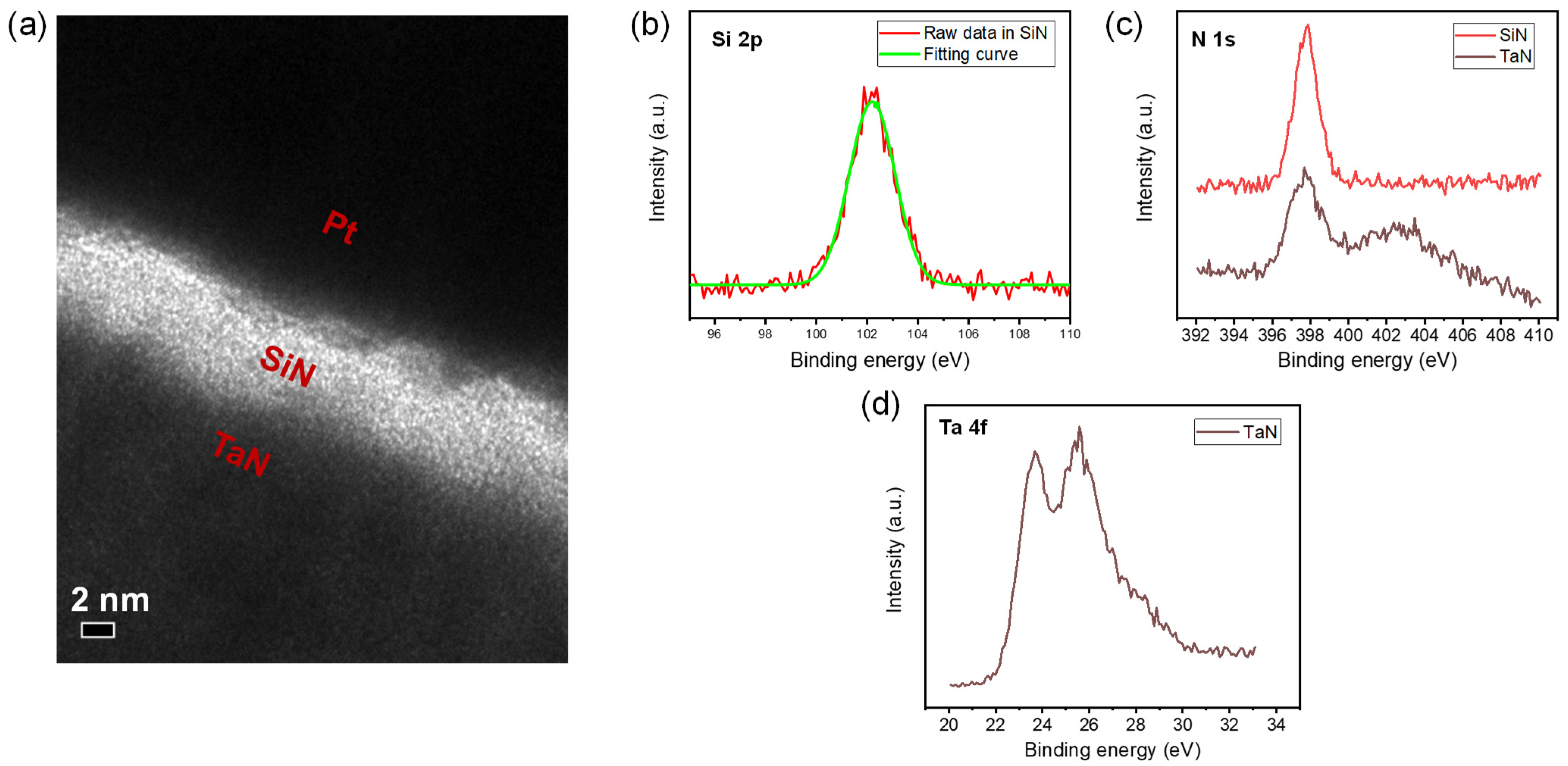
Figure 1 shows a transmission electron microscope (TEM) image of the Pt/SiN/TaN memory device. The thickness of the amorphous SiN layer was about 6 nm. We investigated the XPS spectra of the SiN and TaN layers, and Ar+ etching was used to obtain chemical and material information about these two layers. The sputtering rate was 0.5 nm/s for SiO2. Figure 1b shows Si 2p spectra after an Ar+ etching time of 2 s. The peak binding energy of Si 2p is centered at 102.2 eV for the Si-N bond [14], indicating that the SiN film formed through PECVD did not have the stoichiometry of Si3N4. Figure 1c shows the N 1s spectra after etching times of 2 and 6 s. For the 2 s etching time, the peak of the binding energy was 497.85, corresponding to the Si-N bond. Interestingly, for the 6 s etching time, another peak from 402 to 404 eV was observed for the Ta-N bond [26]. Figure 1d shows Ta 4f spectra for the etching time of 6 s, and doublet peaks of 23.67 and 25.57 eV, corresponding to TaN 4f7/2 and TaN 4f5/2 [26], are evident.
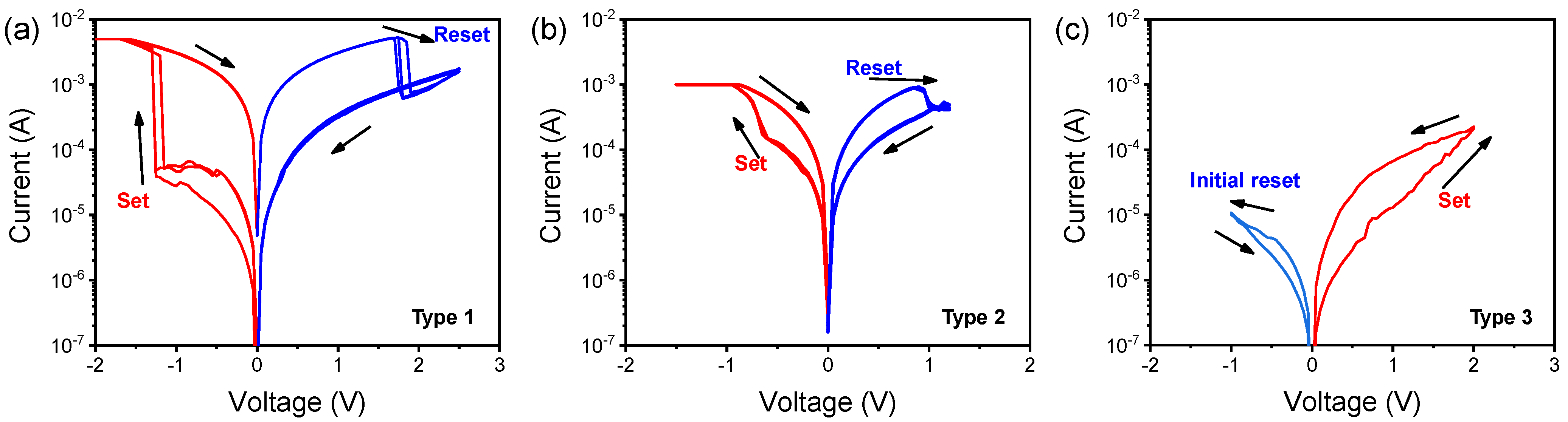
Figure 2a–c show typical I-V curves of the Pt/SiN/TaN device by different switching. This device showed a forming-free process that can eliminate the first process with different voltage conditions because of the presence of numerous traps in SiN, and therefore, the initial state was close to a high-resistance state (HRS). In this study, the conventional sweep mode (no delay between steps, step voltage = 0.05 V) was used. Typical bipolar resistive switching was observed for high-current operation (Figure 2a). The set process occurred at about −1.3 V, and it changed the HRS to a low-resistance state (LRS). The current increased until the compliance current reached 5 mA with an additional voltage sweep. It is noteworthy that a self-compliance current can prevent surges in the current. By contrast, the reset process changed the LRS to a HRS. A decrease in the current was observed for a reset bias sweep. The reset current was comparable to the compliance current. Resistive switching of a SiN-based RRAM can occur by the trapping and de-trapping of an electron in nitride-related traps [18]. Figure 2b shows the lower current operation achieved by limiting the compliance current for typical bipolar resistive switching. We also demonstrate the lowest current operation by using an NDR with a negative bias, and it is shown in Figure 2c. An initial reset was observed, and it could be attributed to the presence of a sufficient number of initial traps in the SiN film. Subsequently, the set process was observed for a positive bias. Similar characteristics have been previously observed for a Pt/Al2O3/TiN memory device [27].
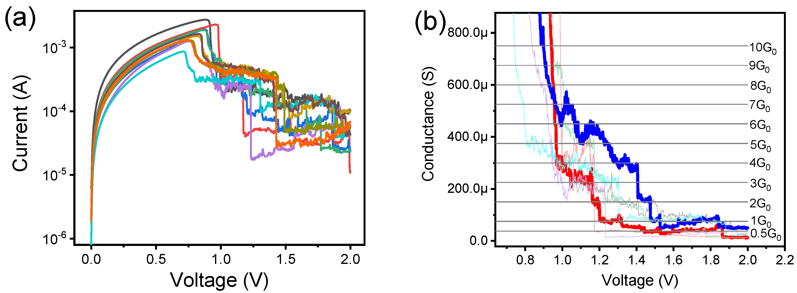
Figure 3a shows I-V curves for the slow sweep measurement mode (delay time = 0.1 s, step voltage = 0.002 V); the quantized effect on the reset process is evident. A decrease in the current is observed over several steps during the reset process. Figure 3b shows conductance-voltage curves for the reset process. G0 = 2e2/h is the quantum of conductance (77.5 μs) [28], where e is the electron charge and h is Planck’s constant. Although the behavior of the reset process is quite different owing to large randomness, the quantized effect can be clearly observed in a few cycles. The red curve in Figure 3b shows the conductance decreasing gradually in a quantized manner (4G0 → 3G0 → 2G0 → 1G0 → 0.5G0). Similarly, the blue curve shows the conductance decreasing (5G0 → 4G0 → 2G0 → 1G0) in a stepwise manner. Multiple conductance states are useful to hardware neuromorphic systems [29,30,31,32,33,34,35].
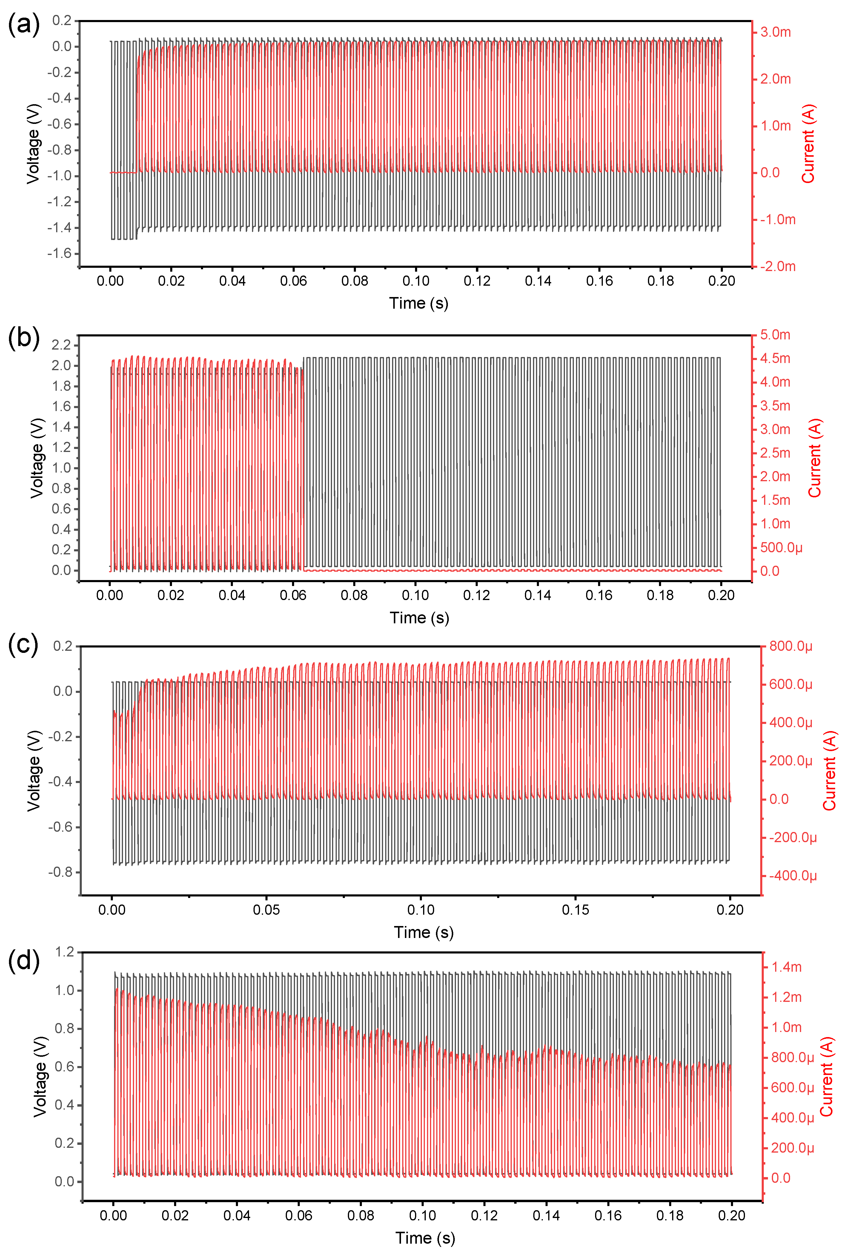
Figure 4 shows the pulse train to clearly observe current modulation by the applied voltage for practical operation of the memory devices. First, the pulses were applied after the switching type was determined on the basis of the DC sweep. The total pulse number was 100 for each case, the width of each pulse was 0.1 ms, and the rise and fall times were 0.01 ms. Figure 4a,b show the set and reset processes for type 1 at pulse voltages of −1.5 and 2 V, respectively. An abrupt transition occurred for both processes. Figure 4c,d show the transient characteristics of the pulse train for type 2. Compared with the set and reset processes of type 1, type 2 showed a more gradual transition.
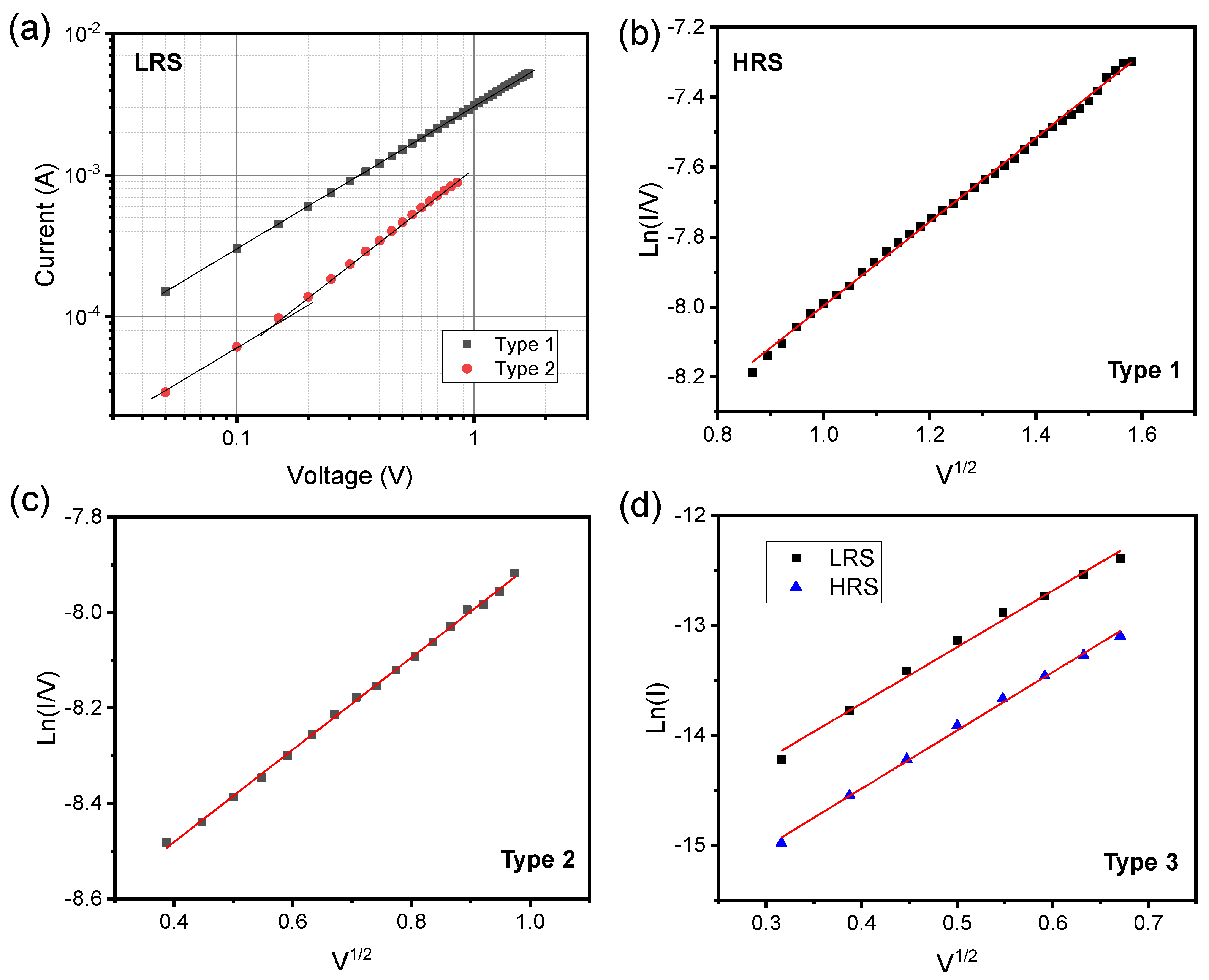
Next, the conduction mechanism was investigated by I-V fitting for the aforementioned three switching types. Figure 5a shows a log–log fit to the type 1 I-V curve for the LRS. A slope of 1 is observed for Ohmic conduction, indicating that the current could flow through a strong silicon conducting filament in the SiN film. Before the reset process, the slope for the LRS for type 2 exceeded 1. On the other hand, the Poole-Frenkel emission fitting (In(I/V) versus V1/2) [36] matched the HRS of types 1 and 2 well (Figure 5d). An electron was exited from traps in the SiN film to the conduction band. Figure 5c shows the Schottky emission fitting (ln(I) versus V1/2) [36] for low current switching in the LRS and HRS. A gradual resistance change was achievable through the modulation of the Schottky barrier for MLC.
4. Conclusions
In summary, a Pt/SiN/TaN memristor device was fabricated and characterized by DC sweep and pulse operation. Component analysis of the SiN/TaN stack was performed, and the SiN thickness was determined from a high-resolution TEM image. Three typical resistive switchings were classified by compliance current and polarity control. Gradual resistive switching was achieved at a compliance current of 1 mA, and the gradual increase and decrease of the current are verified by the pulse train. Moreover, the effect of quantized conductance on the multistep reset process was investigated by reducing the DC sweep speed. The resulst are expected to be applicable to hardware based neuromorphic applications. Finally, the conduction mechanisms of different switching types were determined by I-V fitting.
Author Contributions
J.P. and S.L. conducted the electrical measurements, K.L. validated the data and S.K. wrote the manuscript, designed the experiment, and supervised the study. All authors have read and agreed to the published version of the manuscript.
Funding
This work was supported in part by a National Research Foundation of Korea (NRF) grant funded by the Ministry of Science and ICT, Korea (2021K1A3A1A49098073).
Institutional Review Board Statement
Not applicable.
Informed Consent Statement
Not applicable.
Data Availability Statement
Not applicable.
Conflicts of Interest
The authors declare no conflict of interest.
References
- Lanza, M.; Wong, H.-S.P.; Pop, E.; Ielmini, D.; Strukov, D.; Regan, B.C.; Larcher, L.; Villena, M.A.; Yang, J.J.; Goux, L.; et al. Recommended Methods to Study Resistive Switching Devices. Adv. Electron. Mater. 2018, 5, 1800143. [Google Scholar] [CrossRef] [Green Version]
- Pan, F.; Gao, S.; Chen, C.; Song, C.; Zeng, F. Recent progress in resistive random access memories: Materials, switching mechanisms, and performance. Mater. Sci. Eng. R Rep. 2014, 83, 1–59. [Google Scholar] [CrossRef]
- Mikhaylov, A.; Belov, A.; Korolev, D.; Antonov, I.; Kotomina, V.; Kotina, A.; Gryaznov, E.; Sharapov, A.; Koryazhkina, M.; Kryukov, R.; et al. Multilayer Metal-Oxide Memristive Device with Stabilized Resistive Switching. Adv. Mater. Technol. 2020, 5, 1900607. [Google Scholar] [CrossRef]
- Waser, R.; Dittmann, R.; Staikov, G.; Szot, K. Redox-Based Resistive Switching Memories–Nanoionic Mechanisms, Prospects, and Challenges. Adv. Mater. 2009, 21, 2632–2663. [Google Scholar] [CrossRef]
- Shen, Z.; Zhao, C.; Qi, Y.; Xu, W.; Liu, Y.; Mitrovic, I.Z.; Yang, L.; Zhao, C. Advances of RRAM Devices: Resistive Switching Mechanisms, Materials and Bionic Synaptic Application. Nanomaterials 2020, 10, 1437. [Google Scholar] [CrossRef] [PubMed]
- Jo, S.H.; Chang, T.; Ebong, I.; Bhadviya, B.B.; Mazumder, P.; Lu, W. Nanoscale memristor device as synapse in neuromorphic. Nano Lett. 2010, 10, 1297–1301. [Google Scholar] [CrossRef] [PubMed]
- Jeong, D.S.; Schroeder, H.; Waser, R. Coexistence of Bipolar and Unipolar Resistive Switching Behaviors in a Pt∕TiO2∕Pt Stack. Electrochem. Solid State Lett. 2007, 10, G41. [Google Scholar] [CrossRef]
- Choi, J.; Kim, S. Nonlinear Characteristics of Complementary Resistive Switching in HfAlOx-Based Memristor for High-Density Cross-Point Array Structure. Coatings 2020, 10, 765. [Google Scholar] [CrossRef]
- Jeon, H.; Park, J.; Jang, W.; Kim, H.; Kang, C.; Song, H.; Kim, H.; Seo, H.; Jeon, H. Stabilzed resistive switching behaviors of a Pt/TaOx/TiN RRAM under different oxygen contents. Phys. Status Solidi 2014, 211, 2189–2194. [Google Scholar] [CrossRef]
- Ryu, H.; Kim, S. Implementation of a reservoir computing system using the short-term effects of Pt/HfO2/TaOx/TiN memristors with self-rectification. Chaos Solitons Fractals 2021, 150, 111223. [Google Scholar] [CrossRef]
- Ismail, M.; Chand, U.; Mahata, C.; Nebhen, J.; Kim, S. Demonstration of synaptic and resistive switching characteristics in W/TiO2/HfO2/TaN memristor crossbar array for bioinspired neuromorphic computing. J. Mater. Sci. Technol. 2022, 96, 94–102. [Google Scholar] [CrossRef]
- Prakash, A.; Jana, D.; Maikap, S. TaOx-based resistive switching memories: Prospective and challenges. Nanoscale Res. Lett. 2013, 8, 418. [Google Scholar] [CrossRef] [Green Version]
- Yen, T.-J.; Chin, A.; Gritsenko, V. Improved Device Distribution in High-Performance SiNx Resistive Random Access Memory via Arsenic Ion Implantation. Nanomaterials 2021, 11, 1401. [Google Scholar] [CrossRef]
- Kim, S.; Chang, Y.F.; Kim, M.H.; Park, B.G. Improved resistive switching characteristics in Ni/SiNx/p++-Si devices by tuning x. Appl. Phys. Lett. 2017, 111, 033509. [Google Scholar] [CrossRef]
- Kim, S.; Jung, S.; Kim, M.H.; Chen, Y.C.; Chang, Y.F.; Ryoo, K.C.; Cho, S.; Lee, J.H.; Park, B.G. Scaling Effect on Silicon Nitride Memristor with Highly Doped Si Substrate. Small 2018, 14, 1704062. [Google Scholar] [CrossRef]
- Tikhov, S.V.; Mikhaylov, A.N.; Belov, A.I.; Korolev, D.S.; Antonov, I.N.; Karzanov, V.V.; Gorshkov, O.N.; Tetelbaum, D.I.; Karakolis, P.; Dimitrakis, P. Role of highly doped Si substrate in bipolar resistive switching of silicon nitride MIS-capacitors. Microelectron. Eng. 2018, 187, 134–138. [Google Scholar] [CrossRef]
- Gong, T.; Luo, Q.; Xu, X.; Yuan, P.; Ma, H.; Chen, C.; Liu, Q.; Long, S.; Lv, H.; Liu, M. Uniformity and Retention Improvement of TaOx-Based Conductive Bridge Random Access Memory by CuSiN Interfacial Layer Engineering. IEEE Electron Device Lett. 2017, 38, 1232–1235. [Google Scholar] [CrossRef]
- Vasileiadis, N.; Karakolis, P.; Mandylas, P.; Ioannou-Sougleridis, V.; Normand, P.; Perego, M.; Komninou, P.; Ntinas, V.; Fyrigos, I.-A.; Karafyllidis, I.; et al. Understanding the role of defects in Silicon Nitride-based resistive switching memories through oxygen doping. IEEE Trans. Nanotechnol. 2021, 20, 356–364. [Google Scholar] [CrossRef]
- Russo, U.; Ielmini, D.; Cagli, C.; Lacaita, A.L. Self-Accelerated Thermal Dissolution Model for Reset Programming in Unipolar Resistive-Switching Memory (RRAM) Devices. IEEE Trans. Electron Devices 2009, 56, 193–200. [Google Scholar] [CrossRef]
- Ryu, H.; Kim, S. Self-Rectifying Resistive Switching and Short-Term Memory Characteristics in Pt/HfO2/TaOx/TiN Artificial Synaptic Device. Nanomaterials 2020, 10, 2159. [Google Scholar] [CrossRef]
- Rao, J.; Fan, Z.; Hong, L.; Cheng, S.; Huang, Q.; Zhao, J.; Xiang, X.; Guo, E.-J.; Guo, H.; Hou, Z.; et al. An Electroforming-Free, Analog Interface-Type Memristor Based on A SrFeOx Epitaxial Heterojunction for Neuromorphic Computing. Mater. Today Phys. 2021, 18, 100392. [Google Scholar] [CrossRef]
- Ryu, J.H.; Kim, B.; Hussain, F.; Ismail, M.; Mahata, C.; Oh, T.; Imran, M.; Min, K.K.; Kim, T.-H.; Yang, B.-D.; et al. Zinc Tin Oxide Synaptic Device for Neuromorphic Engineering. IEEE Access 2020, 8, 130678. [Google Scholar] [CrossRef]
- Ismail, M.; Talib, I.; Huang, C.-Y.; Hung, C.-J.; Tsai, T.-L.; Jieng, J.-H.; Chand, U.; Lin, C.-A.; Ahmed, E.; Rana, A.M.; et al. Resistive switching characteristics of Pt/CeOx/TiN memory device. Jpn. J. Appl. Phys. 2014, 53, 060303. [Google Scholar] [CrossRef]
- Ismail, M.; Mahata, C.; Kim, S. Forming-free Pt/Al2O3/HfO2/HfAlOx/TiN memristor with controllable multilevel resistive switching and neuromorphic characteristics for artificial synapse. J. Alloys Compd. 2022, 892, 162141. [Google Scholar] [CrossRef]
- Ismail, M.; Kim, S. Negative differential resistance effect and dual resistive switching properties in a transparent Ce-based devices with opposite forming polarity. Appl. Surf. Sci. 2020, 530, 147284. [Google Scholar] [CrossRef]
- Zaman, A.; Meletis, E.I. Microstructure and Mechanical Properties of TaN Thin Films Prepared by Reactive Magnetron Sputtering. Coatings 2017, 7, 209. [Google Scholar] [CrossRef] [Green Version]
- Ryu, H.; Kim, S. Synaptic Characteristics from Homogeneous Resistive Switching in Pt/Al2O3/TiN Stack. Nanomaterials 2020, 10, 2055. [Google Scholar] [CrossRef]
- Li, Y.; Long, S.; Liu, Y.; Hu, C.; Teng, J.; Liu, Q.; Lv, H.; Sune, J.; Liu, M. Conductance Quantization in Resistive Random Access Memory. Nanoscale Res. Lett. 2015, 10, 420. [Google Scholar] [CrossRef] [Green Version]
- Chandrasekaran, S.; Simanjuntak, F.M.; Saminathan, S.; Panda, D.; Tseng, T.Y. Improving linearity by introducing Al in HfO2 as a memristor synapse device. Nanotechnology 2019, 30, 445205. [Google Scholar] [CrossRef]
- Wang, I.T.; Chang, C.C.; Chiu, L.W.; Chou, T.; Hou, T.H. 3D Ta/TaOx/TiO2/Ti synaptic array and linearity tuning of weight update for hardware neural network applications. Nanotechnology 2016, 27, 365204. [Google Scholar] [CrossRef] [Green Version]
- Emelyanov, A.V.; Nikiruy, K.E.; Serenko, A.V.; Sitnikov, A.V.; Presnyakov, M.Y.; Rybka, R.B.; Sboev, A.G.; Rylkov, V.V.; Kashkarov, P.K.; Kovalchuk, M.V.; et al. Self-adaptive STDP-based learning of a spiking neuron with nanocomposite memristive weights. Nanotechnology 2020, 31, 045201. [Google Scholar] [CrossRef] [PubMed]
- Mikhaylov, A.; Pimashkim, A.; Pigareva, Y.; Gerasimova, S.; Gryaznov, E.; Shchanikov, S.; Zuev, A.; Talanov, M.; Lavrov, I.; Demin, V.; et al. Neurohybrid memristive CMOS-integrated systems for biosensors and neuroprosthetics. Front. Neurosci. 2020, 14, 358. [Google Scholar] [CrossRef] [PubMed]
- Chen, L.; He, Z.-Y.; Wang, T.-Y.; Dai, Y.-W.; Zhu, H.; Sun, Q.-Q.; Zhang, D.W. CMOS Compatible Bio-Realistic Implementation with Ag/HfO2-Based Synaptic Nanoelectronics for Artificial Neuromorphic System. Electronics 2018, 7, 80. [Google Scholar] [CrossRef] [Green Version]
- Yang, J.; Ryu, H.; Kim, S. Resistive and synaptic properties modulation by electroforming polarity in CMOS-compatible Cu/HfO2/Si device. Chaos Solitons Fractals 2021, 145, 110783. [Google Scholar] [CrossRef]
- Gerasimova, S.A.; Belov, A.I.; Korolev, D.S.; Guseinov, D.V.; Lebedeva, A.V.; Koryazhkina, M.N.; Mikhaylov, A.N.; Kazantsev, V.B.; Pisarchik, A.N. Stochastic Memristive Interface for Neural Signal Processing. Sensors 2021, 21, 5587. [Google Scholar] [CrossRef] [PubMed]
- Chang, Y.F.; Fowler, B.; Chen, Y.C.; Chen, Y.T.; Wang, Y.; Xue, F.; Zhou, F.; Lee, J.C. Intrinsic SiOx-based unipolar resistive switching memory. II. Thermal effects on charge transport and characterization of multilevel programing. J. Appl. Phys. 2014, 116, 043709. [Google Scholar] [CrossRef]
Figure 1.
(a) TEM image of a Pt/SiN/TaN device. XPS spectra of (b) Si 2p, (c) N 1s, and (d) Ta 4f.

Figure 2.
Typical I-V curves at compliance currents of (a) 5 mA and (b) 1 mA for a negative bias for the set process and a positive bias for the reset process. (c) First reset process by negative differential resistance in a negative bias.
Figure 2.
Typical I-V curves at compliance currents of (a) 5 mA and (b) 1 mA for a negative bias for the set process and a positive bias for the reset process. (c) First reset process by negative differential resistance in a negative bias.

Figure 3.
(a) I-V curves for the reset process for a slow DC sweep. (b) Conductance-voltage curves for the quantized effect.
Figure 3.
(a) I-V curves for the reset process for a slow DC sweep. (b) Conductance-voltage curves for the quantized effect.

Figure 4.
Pulse transient characteristics for the (a) set and (b) reset processes for type 1 and the (c) set and (d) reset processes for type 2.
Figure 4.
Pulse transient characteristics for the (a) set and (b) reset processes for type 1 and the (c) set and (d) reset processes for type 2.

Figure 5.
(a) Log–log scale fitting for types 1 and 2 for the LRS. Ln (I/V) versus V1/2 for (b) type 1 and (c) type 2 for the HRS. (d) Ln (I) versus V1/2 for type 3 for the LRS and HRS.
Figure 5.
(a) Log–log scale fitting for types 1 and 2 for the LRS. Ln (I/V) versus V1/2 for (b) type 1 and (c) type 2 for the HRS. (d) Ln (I) versus V1/2 for type 3 for the LRS and HRS.

Publisher’s Note: MDPI stays neutral with regard to jurisdictional claims in published maps and institutional affiliations. |
© 2021 by the authors. Licensee MDPI, Basel, Switzerland. This article is an open access article distributed under the terms and conditions of the Creative Commons Attribution (CC BY) license (https://creativecommons.org/licenses/by/4.0/).
Share and Cite
MDPI and ACS Style
Park, J.; Lee, S.; Lee, K.; Kim, S. Conductance Quantization Behavior in Pt/SiN/TaN RRAM Device for Multilevel Cell. Metals 2021, 11, 1918. https://doi.org/10.3390/met11121918
AMA Style
Park J, Lee S, Lee K, Kim S. Conductance Quantization Behavior in Pt/SiN/TaN RRAM Device for Multilevel Cell. Metals. 2021; 11(12):1918. https://doi.org/10.3390/met11121918
Chicago/Turabian StylePark, Jongmin, Seungwook Lee, Kisong Lee, and Sungjun Kim. 2021. "Conductance Quantization Behavior in Pt/SiN/TaN RRAM Device for Multilevel Cell" Metals 11, no. 12: 1918. https://doi.org/10.3390/met11121918
Note that from the first issue of 2016, this journal uses article numbers instead of page numbers. See further details here.