
Substrate Effects on the Random Lasing Performance of Solution-Processed Hybrid-Perovskite Multicrystal Film


Institute of Information Photonics Technology, Beijing University of Technology, Beijing 100124, China
*
Author to whom correspondence should be addressed.
Crystals 2022, 12(3), 334; https://doi.org/10.3390/cryst12030334
Submission received: 1 February 2022
/
Revised: 22 February 2022
/
Accepted: 23 February 2022
/
Published: 27 February 2022
(This article belongs to the Special Issue Organic Optoelectronics: Photoelectronic Conversion Materials, Physics and Devices)
Abstract
:We report dependence of random lasing performance of directly spin-coated multicrystalline thin films of an organic–inorganic hybrid, halide perovskite CH3NH3PbBr3 (MAPbBr3), on different substrates. It was discovered that random lasing performance is strongly dependent on the surface energy properties of the substrate, which determine the morphology and crystallization properties of the spin-coated film, and will consequently determine its optical scattering and emission properties. Using indium–tin oxide (ITO)-coated glass, fused silica, and tricyclo[5.2.1.02,6] decanedimethanol diacrylate (ADCP)-coated fused silica as the substrate materials, we compared the spectroscopic response of the random lasers and thus justified the photophysical mechanisms involved. The modification of the surface properties of the substrate enables controlling of the MAPbBr3 crystallization and leads to the changing of the random lasing properties. The discoveries herein are also important for the construction of other types of laser devices, where the substrate effects should be considered during the design and preparation of the micro-/nano structures.
1. Introduction
Lasing performance and devices in various forms have been explored extensively for hybrid organic–inorganic perovskites (HOIPs) [1,2,3,4,5,6]. Random lasers based on these materials are also reported on the basis of different random structures and optical mechanisms [7,8,9,10]. Multicrystalline structures with randomly distributed interfaces have supplied the optical scattering centers in most of the cases. Although random lasers are categorized into coherent [11,12,13,14] and incoherent types [15,16,17], reported random lasing processes using HOIPs are mostly based on incoherent processes, so that broad-band emission spectra are observed for these lasers.
The green-emitting CH3NH3PbBr3 (MAPbBr3) is one of the most popular HOIP materials for investigations on lasing devices [18,19,20] because of its high emission efficiency, excellent stability, and easy synthesizing and processing advantages. MAPbBr3 is a directbandgap material with a bandgap energy of about 2.3 eV, which may be excited to produce green light emission. Defects in the crystalline structures of this material may induce slight tuning of the energy band structures [21,22]. However, related studies have mainly focused on the design of the materials, their microstructures, fabrication techniques, and photophysical properties [23,24,25,26]; substrate-related effects have not been considered so far. In this work, we investigate how the surface properties of substrates made of different materials influence the morphological and microscopic compositions of the multicrystalline film of MAPbBr3, and consequently influence its spectroscopic response and random lasing performance. The revealed mechanisms will be helpful for the design and realization of optoelectronic devices, including different forms of lasers, using MAPbBr3 as the active medium.
2. Thin Films of Multicrystalline MAPbBr3 on Different Substrates
Multicrystalline films were produced by spin-coating a solution of MAPbBr3 in N,N-dimethylformamide (DMF) with a concentration 560 mg/mL onto different substrates at a speed of 3000 rpm and a duration of 30 s. The materials for synthesizing MAPbBr3 were purchased from Xi’an Polymer Light Technology Corp. (Xi’an, China) and three different substrates were used: (1) Indium–tin oxide (ITO)-coated glass substrate; (2) Fused silica (FS) substrate; (3) ADCP-coated fused silica (FS) substrate. The precursor solution of ADCP was prepared by mixing 0.7-g tricyclo[5.2.1.02,6] decanedimethanol diacrylate (A-DCP), 0.3-g dipentaerythritol penta-/hexa-acrylate, and 5-mg 2,2–Dimethoxy-2-phenylacetophenone (DMPA) in a 3-mL bottle, which was stirred for 2 h under red light. The solution was then spin-coated onto a clean FS substrate at a speed of 3000 rpm for 30 s and the produced ADCP film was cured under a UV lamp for about 1 min for the ADCP coating finishing process.
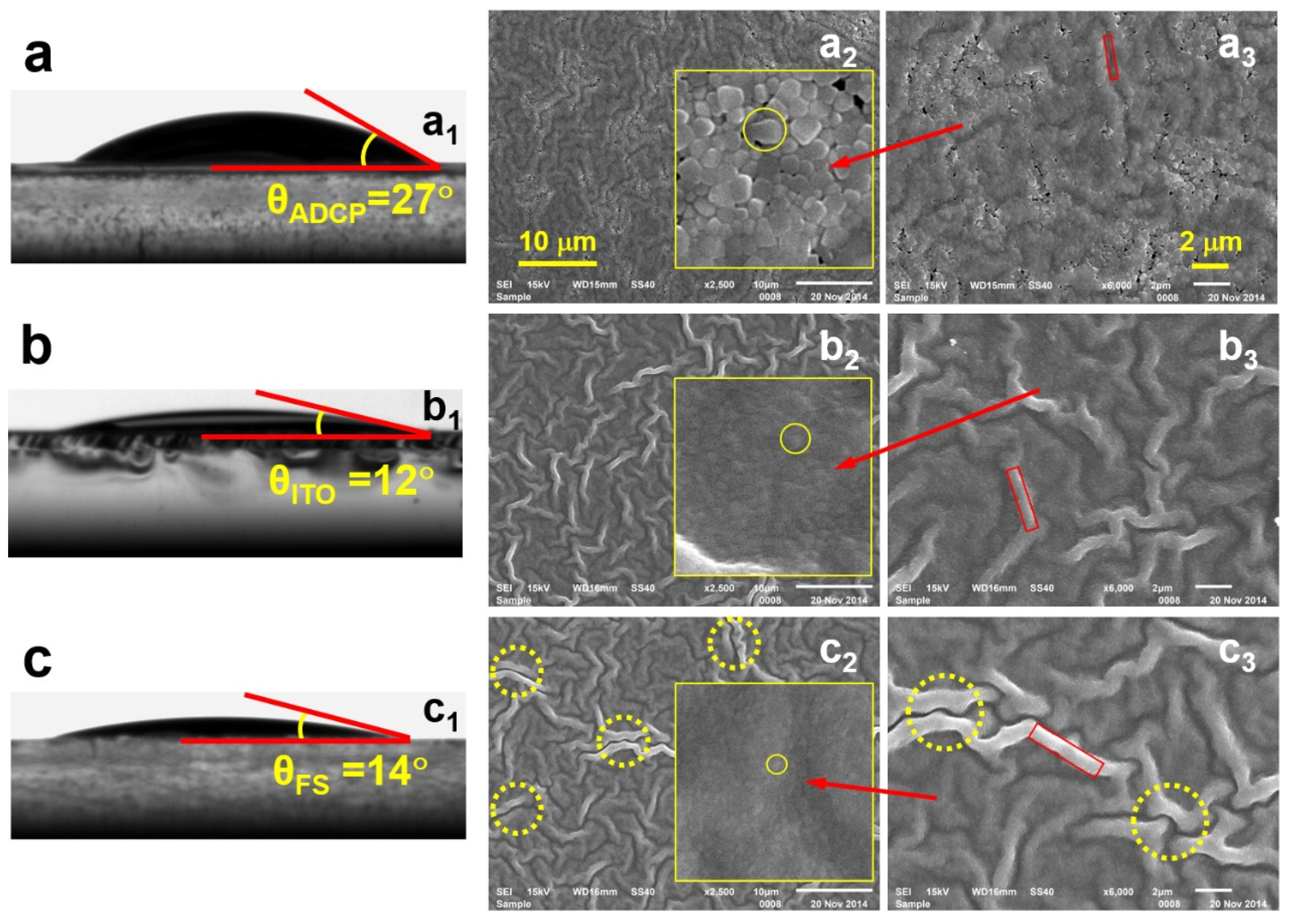
The reason we chose ADCP to modify the surface properties of the substrate is that the ADCP layer has no physical or chemical reactions with the DMF solutions. This can be confirmed by our test experimental results in Figure S1, where the optical microscopic images of an ADCP grating with a period of 4 μm before and after it was immersed in DMF were measured. No changes can be observed in the grating structure due to its interaction with DMF. Therefore, the ADCP-coating on the FS substrate is not destroyed and there is no contamination of MAPbBr3 by ADCP. All these substrates have a thickness of about 1 mm and an area of 15 × 15 mm2. We define these three types of substrates as the ITO substrate, the FS substrate, and the ADCP substrate, respectively, for the convenience of discussion in the following sections. Figure 1a–c shows the characterization of the surface properties of the three substrates and the microscopic properties of the spin-coated MAPbBr3 film on them. Figure 1(a1,b1,c1) shows the contact angle measurements for the MAPbBr3/DMF solution on the ADCP, ITO, and FS substrates, respectively. The corresponding contact angles were measured to be θADCP = 27°, θITO = 12°, θFS = 14°, implying the strongest wetting of the solution was on the ITO substrate and the weakest was on the ADCP. However, the difference is very small between ITO and FS. Such wetting properties directly influence the crystallization properties of MAPbBr3 as it is spin-coated onto these substrates. Figure 1(a2,b2,c2) shows scanning electron microscope images measured on the samples with ADCP, ITO, and FS substrates, respectively, and Figure 1(a3,b3,c3) shows the enlarged views. The insets in Figure 1(a2,b2,c2) show a local-area view, revealing the crystallization details of MAPbBr3 on these three substrates. Furthermore, pinholes and cracks can be clearly observed in Figure 1(a2,a3). The corresponding mechanisms for the formation of such structures can be understood by recent investigations in [22].
According to Figure 1, there are two types of microscopic structures in the multicrystalline films: (1) a randomly distributed crisscross network as a large-scale modulation and as the main feature of the surface morphology; (2) randomly distributed nanoscale crystal particles, as shown in the insets and highlighted by the yellow circles. Clearly, the FS-substrate sample exhibits the thickest wrinkle-like stripes, whereas the ADCP-substrate produces the finest surface morphology with the thinnest modulation. In particular, the modulation exhibits shallow furrows for the ADCP substrate, instead of protruding stripes as for the other substrates. These different features are highlighted by tilted rectangles in red in Figure 1(a3,b3,c3). However, the largest crystal particles are produced in the ADCP-substrate samples and smallest in the FS substrate, as highlighted by yellow circles in the insets in Figure 1(a2,b2,c2). It is understandable that the larger crystal particles in the ADCP-substrate-based sample imply stronger optical scattering, which favors a more efficient random lasing process.
3. Absorption and Photoluminescence (PL) Spectroscopic Properties
Figure 2 shows the absorption and emission spectroscopic properties of the MAPbBr3 multicrystalline films on different substrates. As shown in Figure 2a, the absorption spectrum has the largest amplitude for the ITO substrate and the smallest for the ADCP, if evaluating the measurement data at the peak wavelength of about 525 nm. However, the relationship between them changes when these spectra are normalized at 525 nm, as shown in the inset in Figure 2a. Since the lasing actions take place at wavelengths longer than 540 nm, we also focus our attention on this spectral range. It should be noted that the light-scattering process makes a large contribution to the absorption spectrum in this range. Therefore, the contrast of the spectral feature at 525 nm also reflects, to some extent, the strength of the scattering process. According to the inset of Figure 2a, the sample based on the ADCP substrate exhibits the strongest light-scattering properties, as can be justified by the absorption strength on both sides of the peak wavelength of 525 nm. Meanwhile, the sample based on the FS substrate exhibits the weakest optical scattering, and that on the ITO substrate is located between the other two. This also agrees well with the microscopic observations in the insets in Figure 1(a2,b2,c2). As will be demonstrated in Section 4, these optical scattering processes also agree well with the random lasing properties.
Figure 2b shows the normalized PL spectra measured on the three samples with different substrates. Clearly, the PL spectrum for the ADCP substrate (IADCP(λ)) exhibits the broadest bandwidth and that for the ITO substrate (IITO(λ)) exhibits the narrowest; meanwhile, that for the FS substrate (IFS(λ)) is located within the spectral range of shortest wavelengths. In the Figure 2b inset, we show the calculation results of IADCP(λ)/IITO(λ) and IADCP(λ)/IFS(λ) by the black and red empty circles, respectively. There is a relative enhancement factor of about 1.25 in the PL spectrum by the ADCP-substrate sample at about 556.5 nm with respect to the ITO- and FS-substrate samples, as also highlighted by the arrow in magenta in Figure 2b. This is a stable and well-reproducible mechanism, implying that stronger de-wetting of the solution on the substrate and the consequently larger crystal particles are responsible for the red-shifted and broadened emission spectrum, which also explains the substrate-dependence of the random lasing performance in the subsequent sections. We must stress that the modulation on the PL spectra in Figure 2b did not result from the substrate emission. As shown in Figure S2, where we measured the PL spectra from the three substrates when they are excited by 400-nm femtosecond pulses, no emission from them can be observed. The measured spectra are only composed of background noise.
4. Random Lasing Properties on Different Substrates
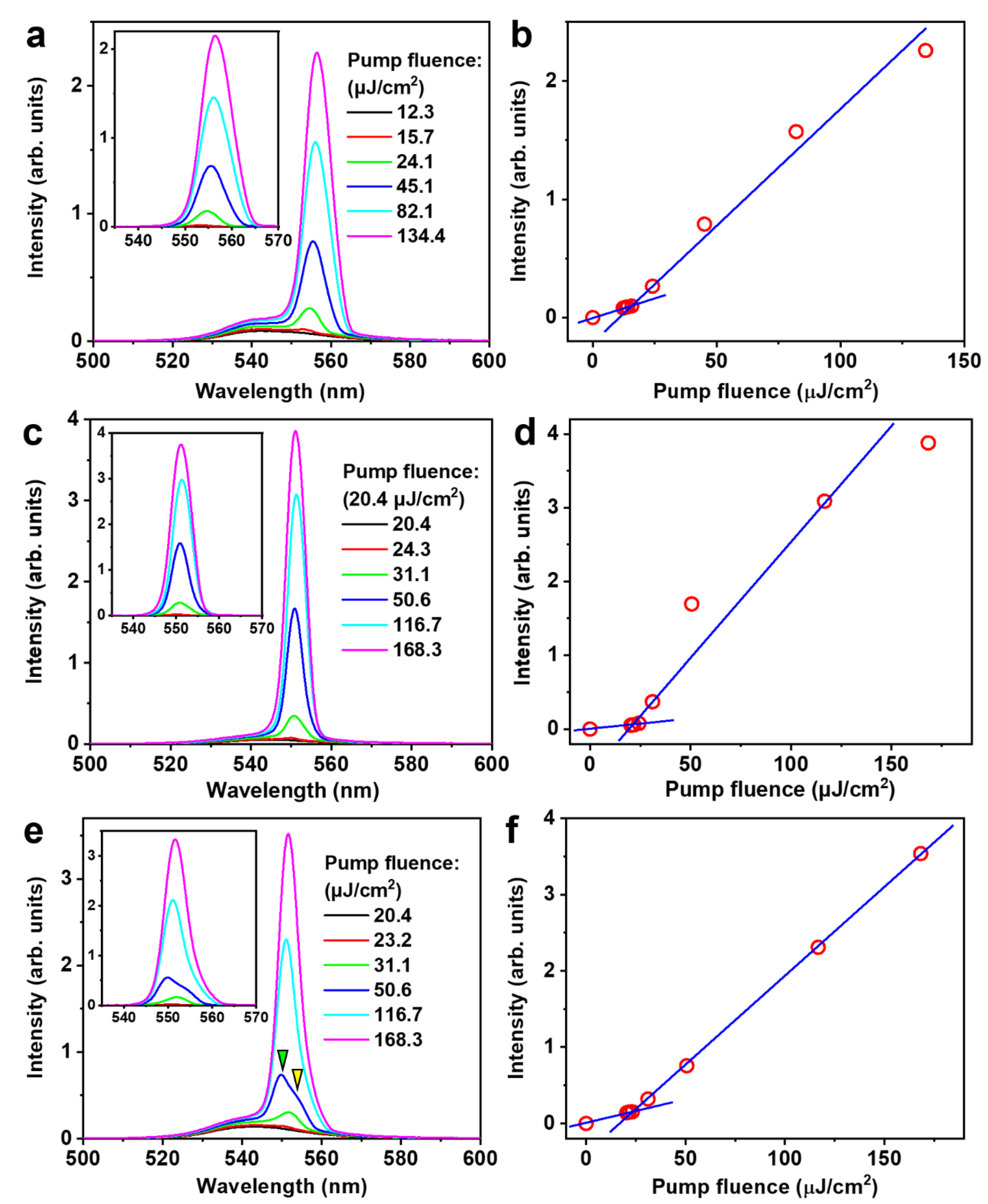
In the investigation on the random lasers, we used 150-fs laser pulses at 400 nm as the pump; these are produced by frequency-doubling of 800-nm pulses from a Ti:sapphire amplifier and have a repetition rate of 1000 Hz. An optical attenuator was placed between the pump laser and the samples of MAPbBr3-coated substrates, so that the pump fluence could be adjusted continuously. A fiber spectrometer was mounted in front of the front surface of the sample so that the detection avoids the reflection of the pump laser beam. Random lasing spectra are measured at different pump fluences, as shown in Figure 3.
Figure 3a shows the random lasing spectra measured on the sample with an ADCP substrate as the pump fluence was increased from 12.3 to 134.4 μJ/cm2. Due to the large variety of the random structures, relatively broader lasing spectra can be observed, where a bandwidth of 7.7 nm at FWHM was measured for a pump fluence of 134.4 μJ/cm2, as shown in the Figure 3a inset. The lasing spectra in the Figure 3a inset have been processed by subtracting the background PL spectra before the random lasing action; therefore, the data in the inset are in fact pure random lasing spectra, where the increase of the pump fluence starts at 15.7 μJ/cm2. Figure 3b plots the random lasing intensity as a function of pump fluence, where two distinct stages can be observed, justifying a pump threshold between 12.3 and 15.7 μJ/cm2.
In Figure 3c,d, we present the experiment results of the samples with an ITO substrate, where we show the pump fluence dependence of the random lasing spectrum and the peak intensity, respectively. From the measurement results, we may measure a peak wavelength of 551.1 nm and a narrower bandwidth of 5.5 nm at FWHM, as shown in the inset in Figure 3c, with respect to the case for an ADCP substrate. However, the pump fluence was found to have increased to between 20.4 and 24.3 μJ/cm2. We may thus understand that large crystal particles in the ADCP-substrate structures led to broadened lasing spectra but lowered pump threshold, where the larger range of the crystal-size distribution facilitates stronger optical scattering in a broader spectrum.
Similar pump threshold performance can be observed with random lasing performance for an FS substrate, which may be estimated between 20.4 and 23.2 μJ/cm2, according to Figure 3e,f. Meanwhile, as shown in the Figure 3e inset, we measured a spectral bandwidth of about 5.97 nm at FWHM for a pump fluence of 168.3 μJ/cm2. However, for the FS substrate we may observe competition between two lasing modes, which can be clearly identified when the pump fluence is lower than 50.6 μJ/cm2. These two lasing modes are located at 551.7 and 554 nm, as highlighted by the green and yellow triangles in Figure 3e, respectively. This feature can be more clearly seen in Figure S3, where we fitted the lasing spectrum at a pump fluence of 50.6 μJ/cm2 using Gaussian functions, so that we were able to decompose the spectral structures. We can clearly see the locations of the PL spectrum (green) centered at 545.2 nm and the two lasing bands peaking at 551.7 (red) and 554 nm (magenta). Although the crystal particles are even smaller on the FS substrate than on the ITO, the wrinkling modulation becomes much larger on the FS substrate, as highlighted by the dashed circles in Figure 1(c2,c3). The occurrence of a second lasing mode may thus be explained by the much-enhanced surface morphology modulation on the FS-substrate, which can be identified by the larger protruding wrinkles than on the other two substrates. The strong scattering by larger centers corresponds to the enhanced gain at longer wavelengths during the interaction between the emissions and excited molecules.
To demonstrate a better comparison between the lasing performance of the samples on three different substrates, we replotted the normalized random lasing spectra at varied pump fluences for the three samples in Figure S4, where we fixed a spectral range of 18 nm for these three groups of data, so that both the tuning range and the bandwidth of the lasing spectrum were comparable for the three samples. We can clearly see that the largest redshift of the lasing spectrum when increasing the pump fluence is produced for the ADCP-substrate sample, as indicated by the red arrow toward the right in Figure S4a. Although a relatively small redshift is observed with the ITO-substrate, there is a definite monotonic redshift (the smaller red arrow toward the right in Figure S3b) of the lasing spectrum when increasing the pump fluence. However, no monotonic shift of the lasing spectrum is observed for the FS substrate when increasing the pump fluence, as highlighted by a double arrow in Figure S4c. This is because there are two lasing modes interacting with each other for the FS substrate. Furthermore, the broadest lasing spectrum is observed for the ADCP substrate, which agrees very well with the microscopic properties of the MAPbBr3 film on ADCP. Large crystal particles, as well as high-density pin-hole and crack defects, have broadened the excitation bands and, consequently, also broadened the lasing spectrum. These defects may induce subbands below the excitation bandedge of the molecules, resulting in new emission features with a red-shifted spectrum. Meanwhile, the consequently stronger optical scattering mechanisms led to a much-reduced lasing threshold for the ADCP substrate, as compared with the other two.
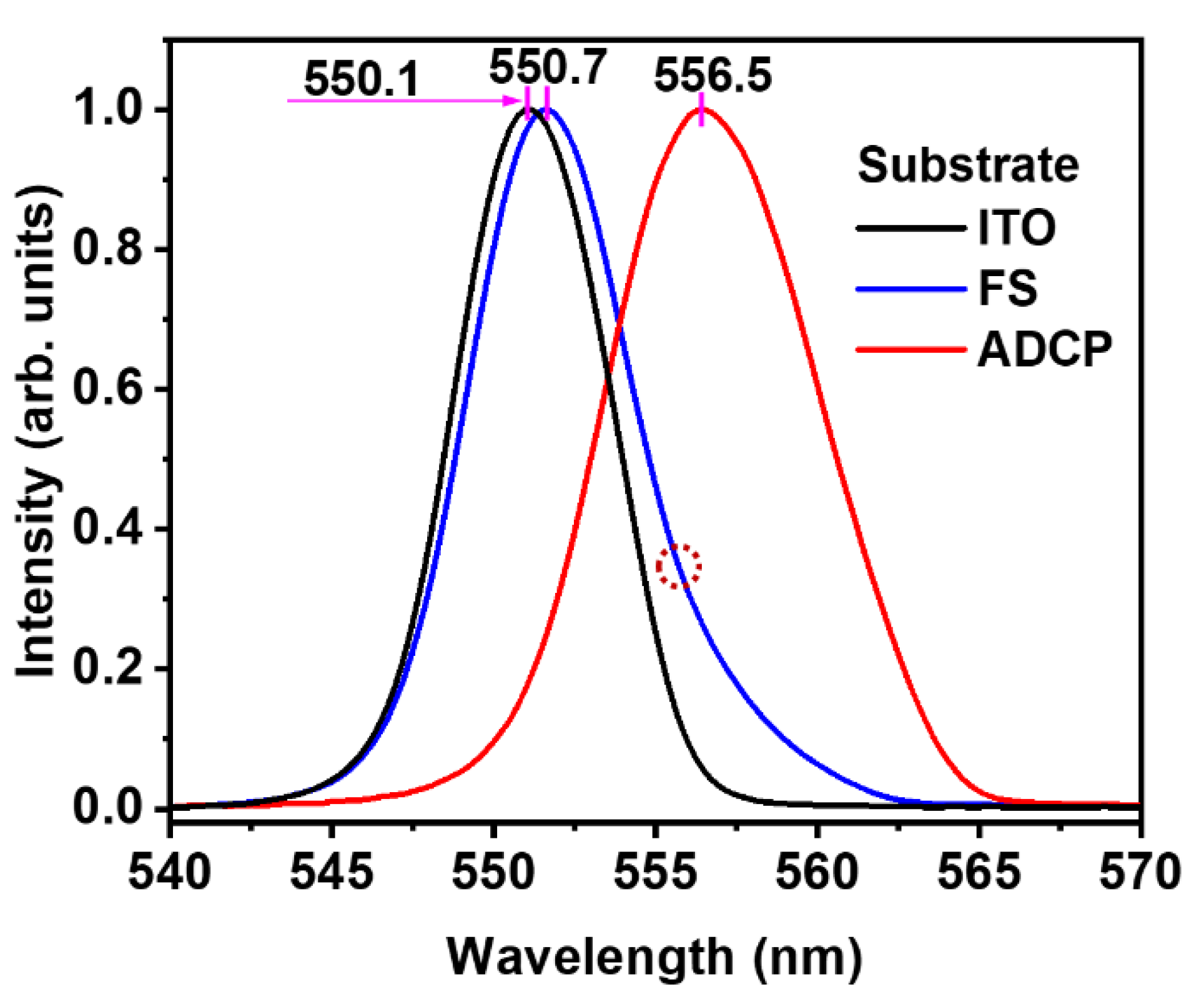
In Figure 4, we make a more detailed comparison between the lasing spectra measured on MAPbBr3 on ADCP, ITO, and FS substrates for pump fluences of 134.4, 168.3, and 168.3 μJ/cm2, respectively. The corresponding peak wavelengths are located at 551.1, 551.7, and 556.5 nm, respectively. The ADCP substrate supports an almost completely separate lasing spectrum from the ITO and FS substrates, which is also the broadest among the three. Although the samples based on the ITO and FS substrates exhibit a quite similar surface morphology, the FS substrate supports a slightly red-shifted and broadened lasing spectrum. More importantly, for the FS substrate, we can still identify an additional feature on the falling edge of the lasing spectrum, as highlighted by a dashed circle, which agrees well with our discussions above regarding the mode competition effect. Therefore, the surface morphological performance of the spin-coated MAPbBr3 film, as well as its spectroscopic response, is very sensitive to the material properties of the substrate.
Furthermore, we may consider the stronger defect sites produced in the ADCP- and FS-substrate samples than those in the ITO-substrate, as shown in Figure 1. The defect states with lowered energy levels in the excitation band are responsible for the new emission features with a red-shifted spectrum. This reasonably explains the red-shifted and broadened random lasing spectrum for the ADCP-substrate sample, as well as a second spectral feature at a longer wavelength for the FS-substrate sample, as has been clearly depicted in Figure S3.
5. Materials and Methods
5.1. Chemicals
Methylamine Bromide (MABr) and Lead (II) Bromide (PbBr2) were purchased from Xi’an Polymer Light Technology Corp., N,N-dimethylformamide (DMF, 99.8%) from Adamas, Tricyclo[5.2.1.02,6] decanedimethanol diacrylate (A-DCP) from SHIN-NAKAMURA CHEMICAL CO, LTD. (Wakayama, Japan), dipentaerythritol penta-/hexa-acrylate from Shanghai Aladdin Biochemical Technology Co., Ltd. (Shanghai, China), and 2,2–Dimethoxy-2-phenylacetophenone (DMPA) from Shanghai Macklin Biochemical Co., Ltd. (Shanghai, China). All regents were used directly without further purification.
5.2. Preparation of the ADCP Substrate
Wash a FS substrate with a size of 15 × 15mm2 and a thickness of 1 mm by TFD 7, deionized water, acetone, and absolute ethanol sequentially for 30 min. Next, blow it with clean nitrogen to dry it. Put the A-DCP, acrylic, and DMPA in a 3 mL bottle to mix them and stir them for 2 h under red light to obtain the ADCP precursor solution. Following this, drop the ADCP solution onto the cleaned FS substrate with a volume of about 10 μL and cover it with another cleaned FS substrate, and clamp together tightly. Finally, place the sandwich structure under the UV lamp for 1 min to complete curing of the ADCP. Remove the FS substrate on the top and finish the preparation of the ADCP substrate on the bottom part.
5.3. Preparation of the ITO and FS Substrates
Wash the ITO or FS substrate by TFD 7, deionized water, acetone, and absolute ethanol sequentially for 30 min. Both types of substrates have a dimension of 15 mm × 15 mm × 1 mm. Blow the cleaned glass substrate with clean nitrogen, until it is dried.
5.4. Synthesis of MAPbBr3
Dissolve equal molar mass of methylamine bromide (MABr) and lead bromide (PbBr2) in 1 mL N,N-dimethylformamide (DMF), heat the mixture at 60 °C and stir it overnight to ensure they are fully dissolved and mixed. The MAPbBr3 solution is thus obtained with a concentration of 0.56 g/mL.
5.5. Preparation of the MAPbBr3 Film on Different Substrates
Spin-coat the solution of MAPbBr3 in DMF with a concentration of 0.56 g/mL onto the ITO, FS, and ADCP substrates in a glove box. The spin-coating speed is 3000 rpm and the duration 30 s, which is the same for all of the samples. Then, place the spin-coated samples on a hotplate and heat them at 80 °C for about 1 min to evaporate the remaining solvent.
5.6. Contact Angle Measurements
Put the cleaned ITO, FS, and ADCP substrates on the sample table of the contact angle measurement instrument from Shanghai FangRui Instrument Co., Ltd. (Shanghai, China), respectively. Drop 2 μL MAPbBr3 solution with a concentration of 0.56 g/mL on each substrate using a microinjector and measure the contact angle using the instrument-equipped software. Capture the displayed picture with the measurement result of the contact angles.
5.7. Measurements on Random Laser Performance
The pump laser source is supplied by a frequency-doubled output from a Ti:sapphire amplifier, which is centered at 400 nm, having a pulse length of about 150 fs and a repetition rate of 1 KHz. The emission spectrum is measured using the Maya2000 Pro fiber spectrometer from Ocean Optics (Dunedin, US), which has a spectral resolution of 0.1 nm.
6. Conclusions
We investigated the dependence of the surface morphology, absorption and emission spectra, and the random lasing properties of the spin-coated organic–inorganic hybrid perovskite MAPbBr3 on the substrate materials. Making using of the efficient photoluminescence properties of MAPbBr3, we were able to achieve random lasing emissions easily in various devices fabricated by direct spin-coating. The bandwidth and location of the random lasing spectrum are found to be tuned by the size of the crystallization particles and by the surface morphologies of the multicrystalline film, which is determined sensitively by the wetting properties of the solution of MAPbBr3 in DMF on the substrates during the spin-coating process. The revealed mechanisms are important for the design and application of solution-processed thin-film laser devices.
Supplementary Materials
The following supporting information can be downloaded at: https://www.mdpi.com/article/10.3390/cryst12030334/s1, Figure S1: Optical microscopic image of an ADCP grating with a period of 4 μm before (a) and after (b) being immersed in DMF; Figure S2: PL spectra of the pure FS, ITO, and ADCP substrates under the excitation of 150 fs pulses at 400 nm. Inset: enlarged view in the studied spectral range from 540 to 560 nm. Only noise is observed in the PL spectra without any typical spectral features; Figure S3: The measured emission spectrum of the ADCP-substrate MAPbBr3 at a pump fluence of 50.6 μJ/cm2 of 400-nm excitation pulses and the multipeak fittings to resolve two distinct random lasing bands peaked at 547.1 and 554 nm by the red and magenta curves, respectively; Figure S4: Pump fluence dependence of the normalized random lasing spectrum for the (a) ADCP, (b) ITO, and (c) FS substrates.
Author Contributions
Author Contribution: Conceptualization, X.Z.; Formal analysis, X.Z.; Funding acquisition, X.Z.; Investigation, J.H.; Methodology, X.Z.; Project administration, X.Z.; Resources, X.Z.; Supervision, X.Z.; Validation, X.Z.; Visualization, X.Z.; Writing—original draft, X.Z.; Writing—review & editing, X.Z. All authors have read and agreed to the published version of the manuscript.
Funding
This research received no external funding.
Acknowledgments
The authors acknowledge the National Natural Science Foundation of China (61735002, 12074020) and Beijing Municipal Education Commission (KZ202010005002) for the support.
Conflicts of Interest
The authors declare no conflict of interest.
References
- Chen, S.S.; Xiao, X.; Chen, B.; Kelly, L.L.; Zhao, J.J.; Lin, Y.Z.; Toney, M.F.; Huang, J.S. Crystallization in One-Step Solution Deposition of Perovskite Films: Upward or Downward? Sci. Adv. 2021, 7, 2412. [Google Scholar] [CrossRef]
- Kim, Y.H.; Kim, S.; Kakekhani, A.; Park, J.; Lee, Y.H.; Xu, H.X.; Nagane, S.; Wexler, R.B.; Kim, D.H.; Jo, S.H.; et al. Comprehensive Defect Suppression in Perovskite Nanocrystals for High-efficiency Light-Emitting Diodes. Nat. Photonics 2021, 15, 148. [Google Scholar] [CrossRef]
- Zhang, Q.; Shang, Q.Y.; Su, R.; Do, T.T.H.; Xiong, Q.H. Halide Perovskite Semiconductor Lasers: Materials, Cavity Design and Low Threshold. Nano Lett. 2021, 21, 1903. [Google Scholar] [CrossRef] [PubMed]
- Liu, Z.Z.; Huang, S.H.; Du, J.; Wang, C.W.; Leng, Y.X. Advances in Inorganic and Hybrid Perovskites for Miniaturized Lasers. Nanophotonics 2020, 9, 2251. [Google Scholar] [CrossRef] [Green Version]
- Hu, J.Y.; Xue, H.B.; Zhang, X.P. Two-Dimensional Crystalline Gridding Networks of Hybrid Halide Perovskite for Random Lasing. Crystals 2021, 11, 1114. [Google Scholar] [CrossRef]
- Hassan, A.; Azam, M.; Ahn, Y.H.; Zubair, M.; Cao, Y.; Khan, A.A. Low Dark Current and Performance Enhanced Perovskite Photodetector by Graphene Oxide as an Interfacial Layer. Nanomaterials 2022, 12, 190. [Google Scholar] [CrossRef]
- Kao, T.S.; Hong, Y.H.; Hong, K.B.; Lu, T.C. Perovskite Random Lasers: A Tunable Coherent Light Source for Emerging Applications. Nanotechnology 2021, 32, 282001. [Google Scholar] [CrossRef]
- Hu, J.Y.; Wang, M.; Tang, F.W.; Liu, M.; Mu, Y.Y.; Fu, Y.L.; Guo, J.X.; Song, X.Y.; Zhang, X.P. Threshold Size Effects in the Patterned Crystallization of Hybrid Halide Perovskites for Random Lasing. Adv. Photonics Res. 2021, 2, 2000097. [Google Scholar] [CrossRef]
- Liu, Y.L.; Yang, W.H.; Xiao, S.M.; Zhang, N.; Fan, Y.B.; Qu, G.Y.; Song, H.Q. Surface-Emitting Perovskite Random Lasers for Speckle-Free Imaging. ACS Nano 2019, 13, 10653. [Google Scholar] [CrossRef] [PubMed]
- Hong, Y.H.; Kao, T.S. Room-Temperature Random Lasing of Metal-Halide Perovskites via Morphology-Controlled Synthesis. Nanoscale Adv. 2020, 2, 5833. [Google Scholar] [CrossRef]
- Wang, C.C.; Kataria, M.; Lin, H.; Nain, A.; Lin, H.Y.; Inbaraj, C.R.; Liao, Y.M.; Thakran, A.; Chang, H.T.; Tseng, F.G.; et al. Generation of Silver Metal Nanocluster Random Lasing. ACS Photonics 2021, 8, 3051. [Google Scholar] [CrossRef]
- Sato, R.; Henzie, J.; Zhang, B.Y.; Ishii, S.; Murai, S.; Takazawa, K.; Takeda, Y. Random Lasing via Plasmon-Induced Cavitation of Microbubbles. Nano Lett. 2021, 21, 6064. [Google Scholar] [CrossRef] [PubMed]
- Zhu, H.Y.; Zhang, W.L.; Zhang, J.C.; Ma, R.; Wang, Z.; Rao, Y.J.; Li, X.F. Single-Shot Interaction and Synchronization of Random Microcavity Lasers. Adv. Mater. Technol. 2021, 6, 2100562. [Google Scholar] [CrossRef]
- Ejbarah, R.A.; Jassim, J.M.; Haddawi, S.F.; Hamidi, S.M. Transition from Incoherent to Coherent Random Lasing by Adjusting Silver Nanowires. Appl. Phys. A 2021, 127, 476. [Google Scholar] [CrossRef]
- Gayathri, R.; Monika, K.; Murukeshan, V.M.; Vijayan, C. Low Threshold Incoherent Random Lasing with Spectral Overlap Optimization of Size-Tuned Plasmonic Nanorods. Opt. Laser Technol. 2021, 139, 106959. [Google Scholar] [CrossRef]
- Okamoto, T.; Mori, M. Random Laser Action in Dye-Doped Polymer Media with Inhomogeneously Distributed Particles and Gain. Appl. Sci. 2019, 9, 3499. [Google Scholar] [CrossRef] [Green Version]
- Yang, T.H.; Chen, C.W.; Jau, H.C.; Feng, T.M.; Wu, C.W.; Wang, C.T.; Lin, T.H. Liquid-crystal random fiber laser for speckle-free imaging. Appl. Phys. Lett. 2019, 114, 191105. [Google Scholar] [CrossRef]
- Giorgi, M.L.; Lippolis, T.; Jamaludin, N.F.; Soci, C.; Bruno, A.; Anni, M. Origin of Amplified Spontaneous Emission Degradation in MAPbBr3 Thin Films under Nanosecond-UV Laser Irradiation. J. Phys. Chem. C 2020, 124, 10696. [Google Scholar] [CrossRef]
- Murzin, A.O.; Stroganov, B.V.; Günnemann, C.; Hammouda, S.B.; Shurukhina, A.V.; Lozhkin, M.S.; Emeline, A.V.; Kapitonov, Y.V. Amplified Spontaneous Emission and Random Lasing in MAPbBr3 Halide Perovskite Single Crystals. Adv. Optical Mater. 2020, 8, 2000690. [Google Scholar] [CrossRef]
- Pourdavoud, N.; Mayer, A.; Buchmüller, M.; Brinkmann, K.; Häger, T.; Hu, T.; Heiderhoff, R.; Shutsko, I.; Görrn, P.; Chen, Y.W.; et al. Distributed Feedback Lasers Based on MAPbBr3. Adv. Mater. Technol. 2018, 3, 1700253. [Google Scholar] [CrossRef]
- Chen, R.X.; Su, X.Q.; Wang, J.; Gao, D.W.; Pan, Y.; Wang, Y.M.; Wang, L. The Roles of Surface Defects in MAPbBr3 and Multi-Structures in MAPbI3. Opt. Mater. 2021, 122, 111600. [Google Scholar] [CrossRef]
- Khan, A.A.; Yu, Z.N.; Khan, U.; Dong, L. Solution Processed Trilayer Structure for High-Performance Perovskite Photodetector. Nanoscale Res. Lett. 2018, 13, 399. [Google Scholar] [CrossRef] [PubMed]
- Ahmad, R.; Surendran, A.; Harikesh, P.C.; Haselsberger, R.; Jamaludin, N.F.; John, R.A.; Koh, T.M.; Bruno, A.; Leong, W.L.; Mathews, N.; et al. Perturbation-Induced Seeding and Crystallization of Hybrid Perovskites over Surface-Modified Substrates for Optoelectronic Devices. ACS Appl. Mater. Interfaces 2019, 11, 27727. [Google Scholar] [CrossRef] [PubMed]
- Gu, Z.K.; Zhou, Z.H.; Huang, Z.D.; Wang, K.; Cai, Z.R.; Hu, X.T.; Li, L.H.; Li, M.Z.; Zhao, Y.S.; Song, Y.L. Controllable Growth of High-Quality Inorganic Perovskite Microplate Arrays for Functional Optoelectronics. Adv. Mater. 2020, 3, 1908006. [Google Scholar] [CrossRef]
- Makarov, S.; Furasova, A.; Tiguntseva, E.; Hemmetter, A.; Berestennikov, A.; Pushkarev, A.; Zakhidov, A.; Kivshar, Y. Halide-Perovskite Resonant Nanophotonics. Adv. Opt. Mater. 2019, 7, 1800784. [Google Scholar] [CrossRef]
- Berestennikov, A.S.; Voroshilov, P.M.; Makarov, S.V.; Kivshar, Y.S. Active Meta-Optics and Nanophotonics with Halide Perovskites. Appl. Phys. Rev. 2019, 6, 031307. [Google Scholar] [CrossRef]
Figure 1.
Substrate surface properties measured on (a) ADCP-coated fused silica, (b) ITO, and (c) fused silica. (a1,b1,c1) Contact angle measurements of the DFM solution of MAPbBr3 on substrates of ADCP, ITO, and FS, respectively. (a2,a3) SEM images of the MAPbBr3-coated ADCP with different magnifications, inset: an enlarged local area. (b2,b3) SEM images of the MAPbBr3-coated ITO with different magnifications, inset: an enlarged local area. (c2,c3) SEM images of the MAPbBr3-coated FS with different magnifications, inset: an enlarged local area.

Figure 2.
(a) Absorption spectra of MAPbBr3 coated on substrates of ADCP, ITO, and FS. Inset: normalized comparison in a selective spectral range. (b) PL spectra of MAPbBr3 on different substrates. Inset: calculated spectra by IADCP(λ)/IITO(λ) and IADCP(λ)/IFS(λ).
Figure 2.
(a) Absorption spectra of MAPbBr3 coated on substrates of ADCP, ITO, and FS. Inset: normalized comparison in a selective spectral range. (b) PL spectra of MAPbBr3 on different substrates. Inset: calculated spectra by IADCP(λ)/IITO(λ) and IADCP(λ)/IFS(λ).

Figure 3.
Random lasing properties measured on MAPbBr3 coated on substrates of (a,b) ADCP, (c,d) ITO, and (e,f) FS. (a,c,e) Directly measured random lasing spectra at different pump fluences. (b,d,f) Pump threshold properties corresponding to substrates ADCP, ITO, and FS, respectively. Insets: Pure random lasing spectra calculated by subtracting the background PL spectrum from the directly measured radiation spectra.

Figure 4.
Comparison between lasing spectra from MAPbBr3 coated on the ITO (black), FS (blue), and ADCP (red) substrates.
Figure 4.
Comparison between lasing spectra from MAPbBr3 coated on the ITO (black), FS (blue), and ADCP (red) substrates.

Publisher’s Note: MDPI stays neutral with regard to jurisdictional claims in published maps and institutional affiliations. |
© 2022 by the authors. Licensee MDPI, Basel, Switzerland. This article is an open access article distributed under the terms and conditions of the Creative Commons Attribution (CC BY) license (https://creativecommons.org/licenses/by/4.0/).
Share and Cite
MDPI and ACS Style
Hu, J.; Zhang, X. Substrate Effects on the Random Lasing Performance of Solution-Processed Hybrid-Perovskite Multicrystal Film. Crystals 2022, 12, 334. https://doi.org/10.3390/cryst12030334
AMA Style
Hu J, Zhang X. Substrate Effects on the Random Lasing Performance of Solution-Processed Hybrid-Perovskite Multicrystal Film. Crystals. 2022; 12(3):334. https://doi.org/10.3390/cryst12030334
Chicago/Turabian StyleHu, Jingyun, and Xinping Zhang. 2022. "Substrate Effects on the Random Lasing Performance of Solution-Processed Hybrid-Perovskite Multicrystal Film" Crystals 12, no. 3: 334. https://doi.org/10.3390/cryst12030334
Note that from the first issue of 2016, this journal uses article numbers instead of page numbers. See further details here.