Biocompatible/Biodegradable Electrowetting on Dielectric Microfluidic Chips with Fluorinated CTA/PLGA


ASIC and System State Key Lab, School of Microelectronics, Fudan University, Shanghai 200433, China
*
Author to whom correspondence should be addressed.
Materials 2018, 11(8), 1332; https://doi.org/10.3390/ma11081332
Submission received: 19 June 2018
/
Revised: 26 July 2018
/
Accepted: 30 July 2018
/
Published: 1 August 2018
(This article belongs to the Special Issue Advances in Hybrid Biomaterials)
Abstract
:One of the major hurdles in the development of biocompatible/biodegradable EWOD (Electrowetting-on-dielectric) devices is the biocompatibility of the dielectric and hydrophobic layers. In this study, we address this problem by using reactive ion etching (RIE) to prepare a super-hydrophobic film combining fluorinated cellulose triacetate (CTA) and poly (lactic-co-glycolic acid) (PLGA). The contact angle (CA) of water droplets on the proposed material is about 160°. X-ray photoelectron spectroscopy (XPS) and atomic force microscopy (AFM) characterizations indicate that a slight increase in the surface roughness and the formation of CFx (C-F or CF2) bonds are responsible for the super-hydrophobic nature of the film. Alternating Current (AC) static electrowetting and droplet transportation experiments evidence that contact angle hysteresis and contact line pinning are greatly reduced by impregnating the CTA/PLGA film with silicon oil. Therefore, this improved film could provide a biocompatible alternative to the typical Teflon® or Cytop® films as a dielectric and hydrophobic layer.
1. Introduction
In recent years, microfluidics has found numerous applications in the biomedical and environmental monitoring fields, for instance, in ecotoxicology [1,2], cell analysis [3,4,5,6], fertilization in vitro (IVF), cell culture [7,8], food detection [9] and soil analysis [10,11]. Due to its low-cost, versatility, and high integration [12,13], electrowetting-on-dielectric (EWOD) is at the forefront of digital microfluidics. EWOD technology can dispense, split, transport and mix droplets on a micro-scale platform under precise control [12,13,14,15,16]. It shows great potential to become one of the key components in future biological systems for sustainable development, such as real time analysis of water and soil quality [17,18], continuous monitoring for agricultural production [19,20,21] and point-of-care medical applications [22,23,24]. Nonetheless, a major issue in the implementation of these bio-systems is the lack of biocompatible/biodegradable EWODs [25,26].
A typical EWOD device consists of a substrate layer (glass or silicon), a driving electrodes layer (ITO, Al, Cu, etc.), a dielectric layer (Su-8, SiO2 etc.) and a hydrophobic/super-hydrophobic layer (e.g., Teflon® or Cytop®) on top of it. When the voltage difference V is applied between a droplet and the electrode, the droplet surface becomes charged and is pulled towards the electrode, reducing the contact angle (CA) of the droplet. For a droplet of non-conducting liquid at mechanical equilibrium and at moderate electric voltage, this phenomenon can be described by the Lippmann-Young (L-Y) equation [27]:
where θ and θ0 are the contact angles with and without voltage V applied, respectively. γ is the surface tension between the liquid and the atmosphere. C (=ε0εd/d) is the capacitance of the dielectric layer, where εd and d are the relative dielectric constant and thickness of the dielectric layer, respectively. ε0 (8.85 × 10⁻¹² F/m) is the vacuum permittivity.
To realize a fully biocompatible/biodegradable EWOD device, the glass/silicon substrate can replaced by polymethyl methacrylate (PMMA) or polydimethylsiloxane (PDMS) [25,28], and the electrodes can be made of biocompatible metals, such as Mn, Mg, etc. The critical point in the device is to fabricate a high-quality dielectric and hydrophobic/super-hydrophobic layer with biocompatible/biodegradable materials.
The main criteria when selecting an optimal material for biocompatible EWOD applications are the ease of processing this material on the substrate surface, the uniformity of the formed layer, the quality of the electrical insulation and the chemical stability of the material. A further requirement for a biodegradable material is to remain chemically stable over a certain timescale and degradable over a longer time. For these reasons, we favored cellulose triacetate (CTA) [29,30] and poly (lactic-co-glycolic acid) (PLGA) [31,32,33] over other choices such as ammonium persulfate (APS, synthesis) [34], poly(3-hydroxybutyrate-co-3-hydroxyhexanoate) (PHBHHx, synthesis) [35,36] and corn proteins (energy-efficient vapor deposition) [37].
In our recent study, we fabricated an EWOD device with a dielectric film composed of a CTA and PLGA mixture [38], while keeping the Teflon®/Cytop® hydrophobic layer. In this paper, we address two problems of this previous embodiment: (i) we enhance the biocompatibility by eliminating the Teflon®/Cytop® hydrophobic layer; and (ii) solve the DC asymmetric electrowetting effect [39,40,41,42,43,44] caused by a higher sensitivity to OH- and other small ions. This is achieved by modifying the CTA/ PLGA dielectric film to cause it to be (super-) hydrophobic.
The (super-) hydrophobic nature of a dielectric film is mainly controlled by its chemical composition and surface geometry [45,46,47,48]. For instance, fluorocarbons CFx (C-F or CF2) on the surface tend to lower the solid surface tension [29,49], while roughness at the micro/nano scale can magnify the hydrophobic nature of the same surface. Depending in the microstructure, there are two types of super-hydrophobicity in nature: the Cassie–Baxter state [50] (best exemplified by the lotus effect) and the Cassie-impregnating state [51] (also called the petal effect). Water droplets are unstable on a lotus leaf, whereas they are pinned to a rose petal, even when turned upside down [51,52]. Both the Cassie–Baxter and Cassie-impregnating state are metastable and turn into the Wenzel state under external interference, such as heat, vibration and electrical fields [53,54,55]. Once the droplet is in the Wenzel state, it is pinned to the surface and can hardly be driven by EWOD forces.
There are several methods to prevent or reverse this Cassie-to-Wenzel transition [56,57]. However, most of them involve external interference that can hardly be integrated into a biocompatible/biodegradable EWOD chip, and might be harmful to the human body. In addition, few of these methods are compatible with the EWOD manipulation of droplets. An option to prevent the Cassie-to-Wenzel transition for a water-based droplet is to infuse a hydrophobic lubricant that strongly wets the solid surface and is immiscible with water [56]. Silicon oil can be applied as the filler in surface pores [57]. This also contributes to reduce the actuation voltage by minimizing the contact angle hysteresis.
In this paper, we will first study the fluorination and microstructuring of the CTA/PLGA surface to fabricate biocompatible/biodegradable dielectric and super-hydrophobic layers for EWOD devices. The CF4/CHF3 reactive ion etching (RIE) process is then analyzed and optimized by etching rate calculations, X-ray photoelectron spectroscopy (XPS), and atomic force microscopy (AFM). The AC static electrowetting test was carried out in air and “air after oil” (substrate dried after impregnation with silicon oil). Eventually, the improved EWOD device will be tested for droplet transportation. Using the PLGA/CTA mixture as both the dielectric and hydrophobic layer involves much lower costs than the traditional materials, such as using SU-8 as dielectrics and Teflon as the hydrophobic layer. In addition, the fabrication process is compatible with the integrated circuits (IC) industry and is suitable for mass production in the future.
2. Materials and Methods
2.1. Materials and Apparatus
The CTA pellets and the PLGA foam (lactide:glycolide = 75:25) were purchased from Sigma-Aldrich Co., Ltd. (St. Louis, MO, USA). Methylene chloride (MC) and N,N-demethylformamide (DMF) provided by Shanghai Chemical Reagent Co., Ltd. (Shanghai, China) were used as the solvents of CTA and PLGA, respectively. Low-viscosity silicone oil (5 mm2/s, 25 °C) was purchased from Sigma-Aldrich to be used as the medium in the measurements. The glass substrate coated with 130 nm of indium tin oxide (ITO) with a sheet resistance of about 15 Ω per square was purchased from Wesley technology Co., Ltd. (Foshan, Guangdong, China).
The spin-coater (WZ-400BZ-6NPP, Laurell Technologies Co., Ltd., North Wales, PA, USA) was used for the deposition of the dielectric layer. The hot plate and the oven (SmartLab HP-303DU, Strider Instrument & Application Co., Ltd., Shanghai, China) were used for post-baking and hard-baking, respectively. To modify the surface wettability of the dielectric layers, a reactive ion etcher (RIE-10NR, Samco International, Kyoto, Japan) was utilized.
The thickness of the film was measured by profilometer (Dektak XT, BRUKER, Karlsruhe, Germany). The surface elemental composition was analyzed by XPS (Thermo ScientificTM K-AlphaTM, Thermo Fisher Scientific Co., Ltd., Waltham, MA, USA). The surface roughness was observed by AFM (Bruker DI D3100, BRUKER, Karlsruhe, Germany). The CA measurements were carried out by the droplet shape analyzer (DSA30, KRUSS, Hamburg, Germany). The driving signals for electrowetting and droplet manipulation were provided by the signal generator (FG503, MOTECH, Tainan, Taiwan) and the amplifier (HA-45, MOTECH, Tainan, Taiwan).
2.2. Preparation and Measurements
In the experiments, the ITO glass substrates were cleaned in acetone, ethanol and deionized (DI) water successively, and dried out with pure N2. The CTA pellets were dissolved in MC, producing a 1.2 wt. % solution, and the PLGA foam was dissolved in DMF, producing a 10 wt. % solution. These two solutions were mixed together with a ratio of MC/DMF (80/20 by volume). The mixture was spin-coated on the ITO glass substrate at 4000 rpm for 45 s. Then these samples were cured in an oven at 100 °C for 30 min. We repeated the coating and curing steps as many times as necessary to reach the desired thickness.
A CF4 plasma treatment had previously been applied to the surface of the CTA and PLGA separately, as in Table 1. It was found that the PLGA film was etched by CF4 [58] and became thinner by 100 nm (under 10 sccm, 50 W, 2.0 Pa CF4 plasma treatment), while the thickness of the CTA film increased slightly due to the deposition of CF4 instead of etching [29]. Both of the surfaces became hydrophobic after the RIE.
After trials of different parameters, an optimized RIE workflow to introduce CFx into the PLGA was defined in the four steps shown in Table 2. Each step has to be carried out successively on the dielectric coatings directly through CF4 plasma treatment under different gas flow rates and power levels. In the last step, CHF3 gas was used instead of CF4 to decrease the roughness of the modified surface. The thickness of the samples was measured during the process, and after each step the atomic composition of carbon/oxygen/fluorine (C/O/F) and their chemical bonds were characterized by XPS. In addition, the surface roughness was analyzed by AFM. The effects of each step are explained in Table 3.
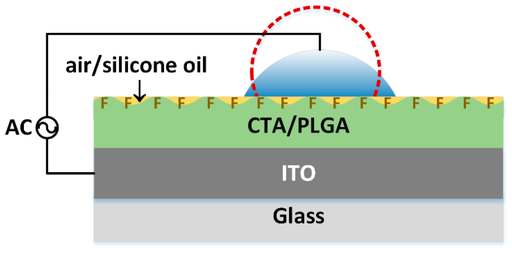
The CA measurements were performed on two types of substrates. Dry substrates “air” were tested directly after fabrication, whereas “air after oil” substrates were first immersed in silicone oil and left to dry naturally. A 6 μL Deionization (DI) water droplet was placed on the surface of “air” or “air after oil” and exposed to an alternating voltage (AC) between a conductive wire and the grounded ITO electrode, as shown in Figure 1. The shape of the droplet was captured and analyzed to obtain the CAs.
The droplet transportation test was carried out using an “air after oil” EWOD chip with patterned electrodes. AC voltage was applied to the electrodes with a certain sequence to manipulate the droplet. The process was captured and the relationship between the transporting velocity and the AC signal was obtained.
3. Results and Discussion
3.1. Etching Rate
The RIE was utilized to enhance the hydrophobicity of CTA/PLGA coatings. During this process, the PLGA was etched through a reaction with CF4 plasma. The etching rate of the mixed dielectrics was calculated.
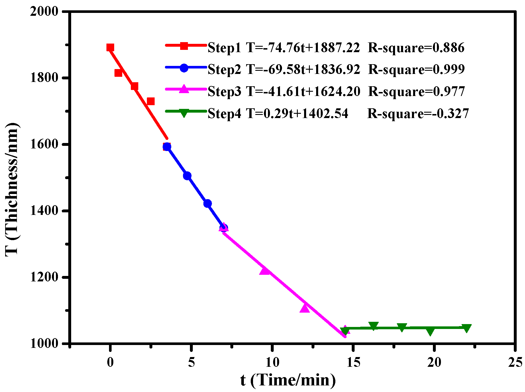
Figure 2 shows the etching rate under different flow and power rates, obtained by linear fitting. In steps 1–3, with the decrease of plasma power (from 100 to 50 W) and flow rate (from 30 to 10 sccm) of the CF4 gas supply, the etching rate was decreased from 74.76 nm/min in step 1 to 69.58 nm/min during step 2 and 41.61 nm/min in step 3. We believe this decreasing etching rate is due to the rarefaction of the PLGA as it reacts with the plasma. The thickness of the dielectrics showed almost no change (0.29 nm/min) when using CHF3 instead of CF4 in step 4, indicating the absence of etching. The surface roughness was reduced and the amount of fluorocarbons CFx increased during the CHF3 gas treatment on the dielectric surface, which could also cause the thickness fluctuation. Finally, a 1.1 µm thick CTA/PLGA dielectric layer was obtained.
3.2. Mechanisms of the RIE Process
During the RIE process, fluorine atoms react with the mixture surface to form fluorocarbons. By this means, the surface tension was decreased to enhance the hydrophobicity of CTA/PLGA dielectrics.
Table 4 and Table 5 show the XPS narrow scan for C/O/F atoms after each step of the process. Prior to the treatment, we hardly detected any presence of fluorine on the sample. After step 1, the ratio of F atoms increased to 29.7%. The results illustrated that fluorine was introduce into the mixture surface in step 1, and then decreased slightly to 26.2% in step 2, and then increased continually to 36.4% in step 3. Eventually, the fraction of F atoms increased slightly to 40.8% in step 4. During the RIE process, there was a sharp rise in F atoms during CF4 gas treatment, and then the ratio of F atoms was maintained with the CHF3 gas treatment. For more details, the chemical nature of the F bonds is reported in Table 5. The majority (62.3%) of F atoms formed C-F bonds with C atoms, and about 10.4% formed CF2 bonds. Since the samples were preserved in aluminum foils, AlFx was also observed in the XPS analysis.
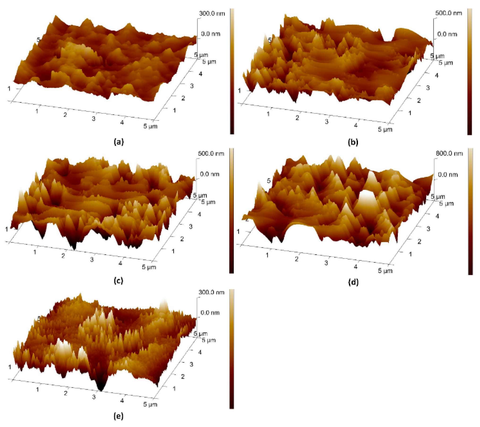
The effect of surface roughness on the wetting property was investigated. Figure 3 shows the AFM scans of these samples. The roughness of the surfaces is detailed in Table 6. The surface roughness was 43.70 nm before RIE (Figure 3e). The roughness increased to 97.90 nm after etching for 3.5 min (Figure 3a), which led to the pinning of the droplet on the surface. To mitigate this effect, the flow rate and power were decreased gradually; the surface roughness increased by 27 nm after 3.5 min etching (Figure 3b) and 84 nm after 7 min etching (Figure 3c). Eventually, the surface was treated with CHF3 to make it smoother (Figure 3d). The final surface roughness was about 66.5 nm. Millimetric droplets (volume > 10 μL) were able to easily slide down the surface.
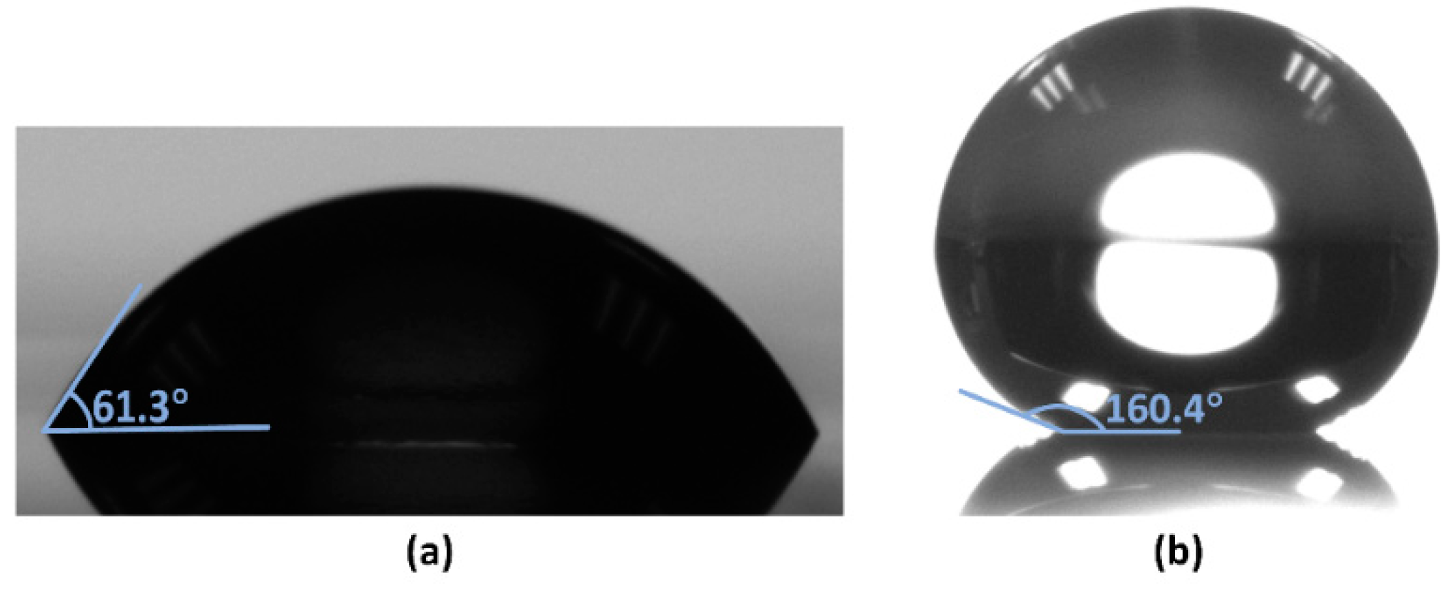
After the ion etching, the CA of the deionized water droplets increased to 160.4°, compared to 61.3° without fluorinated treatment, which indicates that the surface was super-hydrophobic, as shown in Figure 4.
3.3. AC Static Electrowetting Test
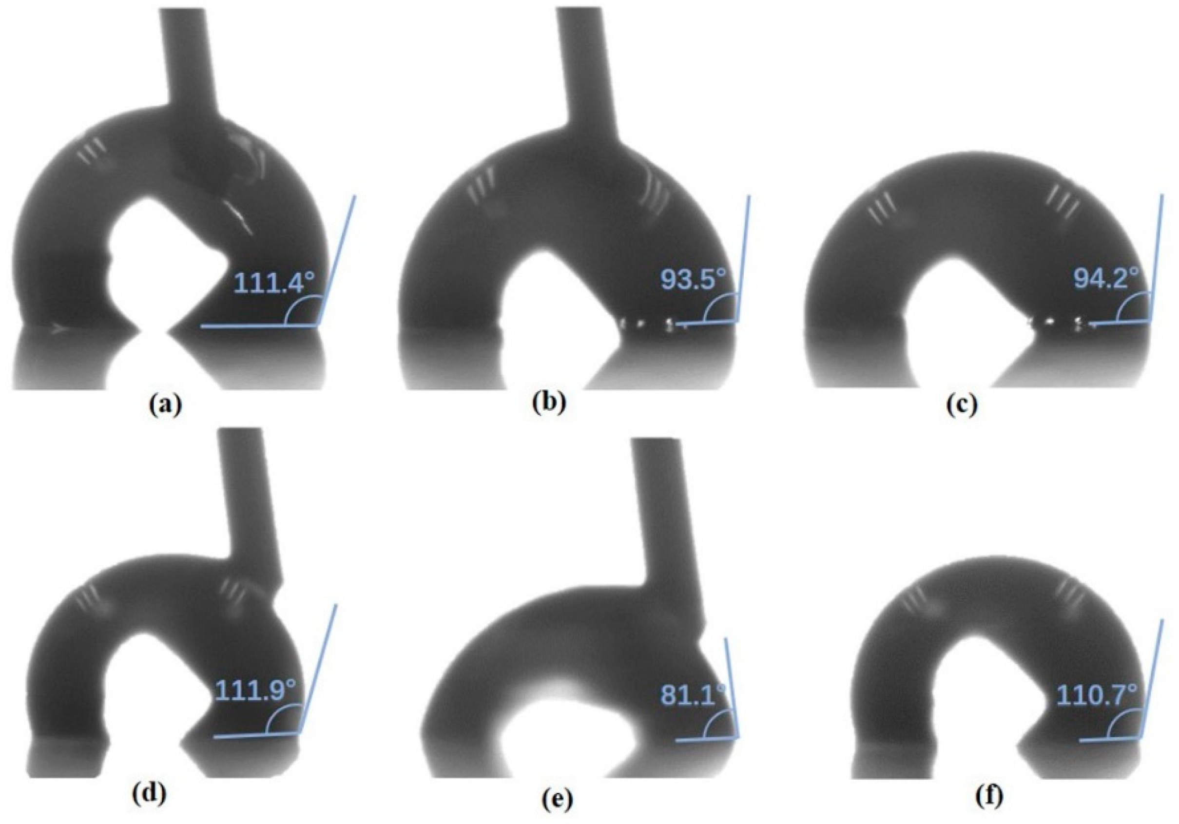
To examine the applicability of the fluorinated CTA/PLGA in EWOD, we first carried out an AC static electrowetting test. Considering the thickness and roughness of the processed mixture coatings, the filler medium in the pores was important [57]. Thus, air and silicone oil were chosen as the medium for this experiment. Figure 5 illustrates the results. When tested in the air directly, the droplet was pinned on the surface even without AC voltage, as seen in Figure 5a. Bubbles emerged on the interface in Figure 5b, which indicates the dielectric breakdown of the 1.1 μm layer under 44Vrms. When the voltage was off, the CA could not be recovered (Figure 5c). In contrast, in the “air after oil” configuration, the droplet moved smoothly on the surface (Figure 5d). With the help of residual oil on the surface, the CA of the DI water droplet decreased (Figure 5e) and reverted to its original value (Figure 5f) when the voltage was on and off. This suggests that the oil filling not only reduces the contact angle hysteresis by smoothing out the chemical imperfections of the surface, but also prevents dielectric breakdown by accumulating some electric charge.
3.4. Droplet Transportation Test
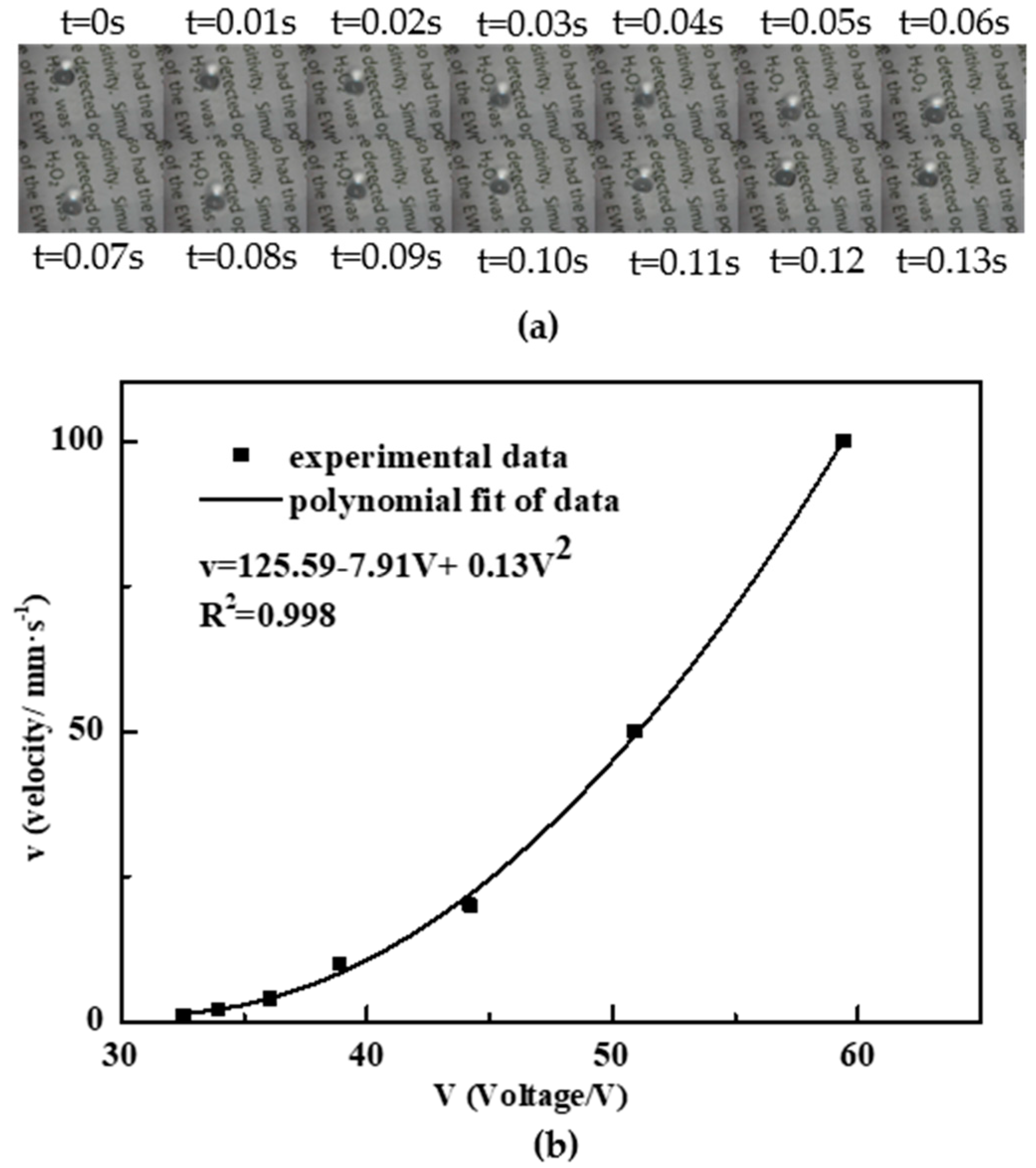
The CTA/PLGA layer was applied to an EWOD transportation chip to verify its ability to act as the dielectric and hydrophobic layer simultaneously. The size of the transporting electrode was 3 mm × 1 mm, with a gap of 30 µm between electrodes. Following the patterning of the electrodes, the EWOD chip was fabricated by the spin coating of CTA/PLGA, RIE and the “air after oil” process, as described above. When a 1 kHz AC voltage was applied to the successive electrodes, the 15-µL droplet moved up and down.
Video (see in Video S1) and images (see Figure 6a) of the process of droplet transportation was recorded. The relationship of the droplet velocity versus voltage (rms) is shown in Figure 6b. Depending on the driving voltage, we achieved droplet velocities from 1 mm/s (30 Vrms) up to 100 mm/s (60 Vrms). The polynomial curve fitting shows that the droplet velocity can be factored into (V − 30)2 within 2% accuracy, indicating an actuation threshold of 30 V, which agreed well with the theoretical properties and practical conclusions of common EWOD chips [60].
4. Conclusions
In this paper, we replaced the hydrophobic Teflon® or Cytop® layer of EWOD systems with a completely biocompatible/biodegradable layer. Using RIE supplied with CF4 and CHF3 gas under different processing parameters, the wettability of the CTA/PLGA mixture surface became super-hydrophobic (CA = 160.4°). XPS and AFM analysis showed that fluorine atoms were introduced onto the surface to form C-F and CF2 bonds. CHF3 was added to reduce the roughness and protect the fluorocarbons on the surface. By this means, a 1.1 μm super-hydrophobic dielectric layer was obtained with about 66.50 nm roughness. The “air after oil” modified surface prevented the pinning of DI water droplets on the surface and protected the dielectrics from breakdown. These digital microfluidic chips showed their suitability and high performance for applications involving bio-systems for sustainable development. The corresponding practical applications will be the subject of future studies.
Supplementary Materials
The following are available online at https://www.mdpi.com/1996-1944/11/8/1332/s1, Video S1: Droplet transporting on PLGA/CTA.
Author Contributions
Conceptualization, K.Z. and L.C.; Formal Analysis, K.Z. and L.C.; Investigation, K.Z. and L.C.; Resources, K.Z. and L.C.; Data Curation, K.Z. and L.C.; Writing—Original Draft Preparation, K.Z.; Writing—Review and Editing, J.Z.; Supervision, J.Z.; Project Administration, J.Z.
Funding
This research was funded by the National Science Foundation of Shanghai Municipal with Grant No. 18ZR1402600 and the State Key Lab of ASIC and System, Fudan University with Grant No. 2018MS003.
Acknowledgments
Antoine Riaud was acknowledged for the help in English revising.
Conflicts of Interest
The authors declare no conflict of interest.
References
- Huang, Y.; Persoone, G.; Nugegoda, D.; Wlodkowic, D. Enabling sub-lethal behavioral ecotoxicity biotests using microfluidic Lab-on-a-Chip technology. Sens. Actuators B Chem. 2016, 226, 289–298. [Google Scholar] [CrossRef]
- Akagi, J.; Zhu, F.; Hall, C.J.; Crosier, K.E.; Crosier, P.S.; Wlodkowic, D. Integrated chip-based physiometer for automated fish embryo toxicity biotests in pharmaceutical screening and ecotoxicology. Cytom. A 2014, 85, 537–547. [Google Scholar] [CrossRef] [PubMed] [Green Version]
- Somaweera, H.; Ibraguimov, A.; Pappas, D. A review of chemical gradient systems for cell analysis. Anal. Chim. Acta 2016, 907, 7–17. [Google Scholar] [CrossRef] [PubMed]
- Witters, D.; Vergauwe, N.; Vermeir, S.; Ceyssens, F.; Liekens, S.; Puers, R.; Lammertyn, J. Biofunctionalization of electrowetting-on-dielectric digital microfluidic chips for miniaturized cell-based applications. Lab Chip 2011, 11, 2790–2794. [Google Scholar] [CrossRef] [PubMed]
- Myung, J.H.; Hong, S. Microfluidic devices to enrich and isolate circulating tumor cells. Lab Chip 2015, 15, 4500–4511. [Google Scholar] [CrossRef] [PubMed] [Green Version]
- Fan, B.; Li, X.; Chen, D.; Peng, H.; Wang, J.; Chen, J. Development of Microfluidic Systems Enabling High-Throughput Single-Cell Protein Characterization. Sensors 2016, 16, 232. [Google Scholar] [CrossRef] [PubMed]
- Huang, H.Y.; Shen, H.H.; Chung, L.Y.; Chung, Y.H.; Chen, C.C.; Hsu, C.H.; Fan, S.K.; Yao, D.J. Fertilization of Mouse Gametes In Vitro Using a Digital Microfluidic System. IEEE Trans. Nanobiosci. 2015, 14, 857–863. [Google Scholar] [CrossRef] [PubMed]
- Huang, H.Y.; Shen, H.H.; Tien, C.H.; Li, C.J.; Fan, S.K.; Liu, C.H.; Hsu, W.S.; Yao, D.J. Digital Microfluidic Dynamic Culture of Mammalian Embryos on an Electrowetting on Dielectric (EWOD) Chip. PLoS ONE 2015, 10, e0124196. [Google Scholar] [CrossRef] [PubMed]
- Zhang, Z.; Yu, L.; Xu, L.; Hu, X.; Li, P.; Zhang, Q.; Ding, X.; Feng, X. Biotoxin sensing in food and environment via microchip. Electrophoresis 2014, 35, 1547–1559. [Google Scholar] [CrossRef] [PubMed]
- Date, Y.; Terakado, S.; Sasaki, K.; Aota, A.; Matsumoto, N.; Shiku, H.; Ino, K.; Watanabe, Y.; Matsue, T.; Ohmura, N. Microfluidic heavy metal immunoassay based on absorbance measurement. Biosens. Bioelectron. 2012, 33, 106–112. [Google Scholar] [CrossRef] [PubMed]
- Stanley, C.E.; Grossmann, G.; i Solvas, X.C.; deMello, A.J. Soil-on-a-Chip, Microfluidic platforms for environmental organismal studies. Lab Chip 2016, 16, 228–241. [Google Scholar] [CrossRef] [PubMed]
- Banerjee, A.; Liu, Y.; Heikenfeld, J.; Papautsky, I. Deterministic splitting of fluid volumes in electrowetting microfluidics. Lab Chip 2012, 12, 5138–5141. [Google Scholar] [CrossRef] [PubMed]
- Chong, Z.Z.; Tan, S.H.; Ganan-Calvo, A.M.; Tor, S.B.; Loh, N.H.; Nguyen, N.T. Active droplet generation in microfluidics. Lab Chip 2016, 16, 35–58. [Google Scholar] [CrossRef] [PubMed]
- Yafia, M.; Shukla, S.; Najjaran, H. Fabrication of digital microfluidic devices on flexible paper–based and rigid substrates via screen printing. J. Micromech. Microeng. 2015, 25, 057001. [Google Scholar] [CrossRef]
- Teh, S.Y.; Lin, R.; Hung, L.H.; Lee, A.P. Droplet microfluidics. Lab Chip 2008, 8, 198–220. [Google Scholar] [CrossRef] [PubMed]
- Li, Y.; Baker, R.J.; Raad, D. Improving the performance of electrowetting on dielectric microfluidics using piezoelectric top plate control. Sens. Actuators B Chem. 2016, 229, 63–74. [Google Scholar] [CrossRef]
- Khoshmanesh, K.; Zhang, C.; Tovar-Lopez, F.J.; Nahavandi, S.; Baratchi, S.; Kalantar-zadeh, K.; Mitchell, A. Dielectrophoretic manipulation and separation of microparticles using curved microelectrodes. Electrophoresis 2009, 30, 3707–3717. [Google Scholar] [CrossRef] [PubMed]
- Baek, C.; Kim, H.Y.; Na, D.; Min, J. A microfluidic system for the separation and detection of E. coli O157:H7 in soil sample using ternary interactions between humic acid, bacteria, and a hydrophilic surface. Sens. Actuators B Chem. 2015, 208, 238–244. [Google Scholar] [CrossRef]
- Doe, J. Evaluation of a Microfluidic Paper-based Device for Determination of Reactive Phosphate in Soil Solution. Available online: http://dx.doi.org/10.2134/csa2014-59-6-5 (accessed on 30 July 2018).
- Duford, D.A.; Xi, Y.; Salin, E.D. Enzyme inhibition-based determination of pesticide residues in vegetable and soil in centrifugal microfluidic devices. Anal. Chem. 2013, 85, 7834–7841. [Google Scholar] [CrossRef] [PubMed]
- Ali, M.A.; Jiang, H.; Mahal, N.K.; Weber, R.J.; Kumar, R.; Castellano, M.J.; Dong, L. Microfluidic impedimetric sensor for soil nitrate detection using graphene oxide and conductive nanofibers enabled sensing interface. Sens. Actuators B Chem. 2017, 239, 1289–1299. [Google Scholar] [CrossRef]
- Elsharkawy, M.; Schutzius, T.M.; Megaridis, C.M. Inkjet patterned superhydrophobic paper for open-air surface microfluidic devices. Lab Chip 2014, 14, 1168–1175. [Google Scholar] [CrossRef] [PubMed]
- Nayak, S.; Sridhara, A.; Melo, R.; Richer, L.; Chee, N.H.; Kim, J.; Linder, V.; Steinmiller, D.; Sia, S.K.; Gomes-Solecki, M. Microfluidics-based point-of-care test for serodiagnosis of Lyme Disease. Sci. Rep. 2016, 6, 35069. [Google Scholar] [CrossRef] [PubMed] [Green Version]
- Xing, S.; Harake, R.S.; Pan, T. Droplet-driven transports on superhydrophobic-patterned surface microfluidics. Lab Chip 2011, 11, 3642–3648. [Google Scholar] [CrossRef] [PubMed]
- Scholten, K.; Meng, E. Materials for microfabricated implantable devices: A review. Lab Chip 2015, 15, 4256–4272. [Google Scholar] [CrossRef] [PubMed]
- Teixidor, D.; Orozco, F.; Thepsonthi, T.; Ciurana, J.; Rodríguez, C.A.; Özel, T. Effect of process parameters in nanosecond pulsed laser micromachining of PMMA-based microchannels at near-infrared and ultraviolet wavelengths. Int. J. Adv. Manuf. Technol. 2012, 67, 1651–1664. [Google Scholar] [CrossRef]
- Vallet, M.; Berge, B.; Vovelle, L. Electrowetting of water and aqueous solutions on poly (ethylene terephthalate) insulating films. Polymer 1996, 37, 2465–2470. [Google Scholar] [CrossRef]
- Sinclair, J.; Salem, A.K. Rapid localized cell trapping on biodegradable polymers using cell surface derivatization and microfluidic networking. Biomaterials 2006, 27, 2090–2094. [Google Scholar] [CrossRef] [PubMed]
- Yoon, Y.I.; Moon, H.S.; Lyoo, W.S.; Lee, T.S.; Park, W.H. Superhydrophobicity of cellulose triacetate fibrous mats produced by electrospinning and plasma treatment. Carbohydr. Polym. 2009, 75, 246–250. [Google Scholar] [CrossRef]
- Park, C.H.; Kang, Y.K.; Im, S.S. Biodegradability of cellulose fabrics. J. Appl. Polym. Sci. 2004, 94, 248–253. [Google Scholar] [CrossRef]
- King, K.R.; Wang, C.C.J.; Kaazempur-Mofrad, M.R.; Vacanti, J.P.; Borenstein, J.T. Biodegradable Microfluidics. Adv. Mater. 2004, 16, 2007–2012. [Google Scholar] [CrossRef]
- Anderson, J.M.; Shive, M.S. Biodegradation and biocompatibility of PLA and PLGA microspheres. Adv. Drug Deliv. Rev. 2012, 64, 72–82. [Google Scholar] [CrossRef]
- Cho, D.-I.D.; Yoo, H.J. Microfabrication Methods for Biodegradable Polymeric Carriers for Drug Delivery System Applications: A Review. J. Microelectromech. Syst. 2015, 24, 10–18. [Google Scholar] [CrossRef]
- Wang, J.; Bettinger, C.J.; Langer, R.S.; Borenstein, J.T. Biodegradable microfluidic scaffolds for tissue engineering from amino alcohol-based poly (ester amide) elastomers. Organogenesis 2010, 6, 212–216. [Google Scholar] [CrossRef] [PubMed]
- Yang, Y.; Ke, S.; Ren, L.; Wang, Y.; Li, Y.; Huang, H. Dielectric spectroscopy of biodegradable poly (3-hydroxybutyrate-co-3-hydroxyhexanoate) films. Eur. Polym. J. 2012, 48, 79–85. [Google Scholar] [CrossRef]
- Lomas, A.J.; Webb, W.R.; Han, J.; Chen, G.Q.; Sun, X.; Zhang, Z.; El Haj, A.J.; Forsyth, N.R. Poly (3-hydroxybutyrate-co-3-hydroxyhexanoate)/collagen hybrid scaffolds for tissue engineering applications. Tissue Eng. Part C Methods 2013, 19, 577–585. [Google Scholar] [CrossRef] [PubMed]
- Hsiao, A.; Luecha, J.; Kokini, J.; Liu, L. Green microfluidics made of corn proteins. In Proceedings of the 2011 Annual International Conference of the IEEE Engineering in Medicine and Biology Society, Boston, MA, USA, 30 August–3 September 2011; pp. 8400–8403. [Google Scholar] [CrossRef]
- Chao, L.; Zeng, Z.; Zhang, K.; Zhou, J. Application of CTA mixed with PLGA as biocompatible/biodegradable dielectrics in EWOD devices. IEEE Trans. Dielectr. Electr. Insul. 2017, 24, 3132–3137. [Google Scholar] [CrossRef]
- Mats, L.; Bramwell, A.; Dupont, J.; Liu, G.J.; Oleschuk, R. Electrowetting on superhydrophobic natural (Colocasia) and synthetic surfaces based upon fluorinated silica nanoparticles. Microelectron. Eng. 2015, 148, 91–97. [Google Scholar] [CrossRef]
- Moon, H.; Cho, S.K.; Garrell, R.L.; Kim, C.-J.C. Low voltage electrowetting-on-dielectric. J. Appl. Phys. 2002, 92, 4080. [Google Scholar] [CrossRef]
- Seyrat, E.; Hayes, R.A. Amorphous fluoropolymers as insulators for reversible low-voltage electrowetting. J. Appl. Phys. 2001, 90, 1383–1386. [Google Scholar] [CrossRef]
- Fan, S.K.; Yang, H.; Wang, T.T.; Hsu, W. Asymmetric electrowetting-moving droplets by a square wave. Lab Chip 2007, 7, 1330–1335. [Google Scholar] [CrossRef] [PubMed]
- Quinn, A.; Sedev, R.; Ralston, J. Influence of the Electrical Double Layer in Electrowetting. J. Phys. Chem. B 2003, 107, 1163–1169. [Google Scholar] [CrossRef]
- Nanayakkara, Y.S.; Moon, H.; Payagala, T.; Wijeratne, A.B.; Crank, J.A.; Sharma, P.S.; Armstrong, D.W. A fundamental study on electrowetting by traditional and multifunctional ionic liquids: Possible use in electrowetting on dielectric-based microfluidic applications. Anal. Chem. 2008, 80, 7690–7698. [Google Scholar] [CrossRef] [PubMed]
- Brown, P.S.; Talbot, E.L.; Wood, T.J.; Bain, C.D.; Badyal, J.P. Superhydrophobic hierarchical honeycomb surfaces. Langmuir 2012, 28, 13712–13719. [Google Scholar] [CrossRef] [PubMed]
- Woodward, I.; Schofield, W.C.E.; Roucoules, V.; Badyal, J.P.S. Super-hydrophobic Surfaces Produced by Plasma Fluorination of Polybutadiene Films. Langmuir 2003, 19, 3432–3438. [Google Scholar] [CrossRef]
- Jonoobi, M.; Harun, J.; Mathew, A.P.; Hussein, M.Z.B.; Oksman, K. Preparation of cellulose nanofibers with hydrophobic surface characteristics. Cellulose 2009, 17, 299–307. [Google Scholar] [CrossRef] [Green Version]
- Manca, M.; Cortese, B.; Viola, I.; Arico, A.S.; Cingolani, R.; Gigli, G. Influence of chemistry and topology effects on superhydrophobic CF (4)-plasma-treated poly(dimethylsiloxane) (PDMS). Langmuir 2008, 24, 1833–1843. [Google Scholar] [CrossRef] [PubMed]
- Kim, S.H.; Kim, J.H.; Kang, B.K.; Uhm, H.S. Superhydrophobic CFx coating via in-line atmospheric RF plasma of He-CF4-H2. Langmuir 2005, 21, 12213–12217. [Google Scholar] [CrossRef] [PubMed]
- Gong, G.; Wu, J.; Jin, X.; Jiang, L. Adhesion Tuning at Superhydrophobic States: From Petal Effect to Lotus Effect. Macromol. Mater. Eng. 2015, 300, 1057–1062. [Google Scholar] [CrossRef]
- Feng, L.; Zhang, Y.; Xi, J.; Zhu, Y.; Wang, N.; Xia, F.; Jiang, L. Petal effect: A superhydrophobic state with high adhesive force. Langmuir 2008, 24, 4114–4119. [Google Scholar] [CrossRef] [PubMed]
- Cassie, A.B.D.; Baxter, S. Wettability of porous surfaces. Trans. Faraday Soc. 1944, 40, 546–551. [Google Scholar] [CrossRef]
- Koishi, T.; Yasuoka, K.; Fujikawa, S.; Ebisuzaki, T.; Zeng, X.C. Coexistence and transition between Cassie and Wenzel state on pillared hydrophobic surface. Proc Natl Acad Sci USA 2009, 106, 8435–8440. [Google Scholar] [CrossRef] [PubMed] [Green Version]
- Tsai, P.C.; Lammertink, R.G.H.; Wessling, M.; Lohse, D. Evaporation-Triggered Wetting Transition for Water Droplets upon Hydrophobic Microstructures. Phys. Rev. Lett. 2010, 104, 116102. [Google Scholar] [CrossRef] [PubMed] [Green Version]
- Heikenfeld, J.; Dhindsa, M. Electrowetting on Superhydrophobic Surfaces: Present Status and Prospects. J. Adhes. Sci. Technol. 2008, 22, 319–334. [Google Scholar] [CrossRef]
- Papathanasiou, A.G. Progress toward reversible electrowetting on geometrically patterned superhydrophobic surfaces. Curr. Opin. Colloid Interface Sci. 2018, 36, 70–77. [Google Scholar] [CrossRef]
- Pollack, M.G. Electrowetting-Based Microactuation of Droplets for Digital Microfluidics. Ph.D. Thesis, Duke University, Durham, NC, USA, 2001. [Google Scholar]
- Tanaka, K.; Kogoma, M.; Ogawa, Y. Fluorinated polymer coatings on PLGA microcapsules for drug delivery system using atmospheric pressure glow plasma. Thin Solid Films 2006, 506, 159–162. [Google Scholar] [CrossRef]
- Byungwhan, K.; Byung-Teak, L. Relationships between etch rate and roughness of plasma-etched surface. IEEE Trans. Plasma Sci. 2002, 30, 2074–2077. [Google Scholar] [CrossRef]
- Song, J.H.; Evans, R.; Lin, Y.Y.; Hsu, B.N.; Fair, R.B. A scaling model for electrowetting-on-dielectric microfluidic actuators. Microfluid. Nanofluid. 2008, 7, 75–89. [Google Scholar] [CrossRef]
Figure 1.
Schematics of CA measurement with the filler medium of air or silicone oil.

Figure 2.
Change of dielectric thickness after RIE steps 1–4.

Figure 3.
AFM scanning images of (a) step 1, (b) step 2, (c) step 3, (d) step 4 and (e) untreated.

Figure 4.
DI water droplet on the mixture film (a) untreated and (b) fluorinated by RIE.

Figure 5.
AC static electrowetting test in the air under (a) AC off (b) 44Vrms (c) AC off again, and in the “air after oil” under (d) AC off (e) 44Vrms (f) AC off again.
Figure 5.
AC static electrowetting test in the air under (a) AC off (b) 44Vrms (c) AC off again, and in the “air after oil” under (d) AC off (e) 44Vrms (f) AC off again.

Figure 6.
Electrowetting transportation test: (a) images of droplet transportation; (b) droplet velocity versus voltage (r.m.s).
Figure 6.
Electrowetting transportation test: (a) images of droplet transportation; (b) droplet velocity versus voltage (r.m.s).


Table 1.
Effects of the CF4 treatment on CTA and PLGA separately.
| Material | Property | CF4 Treatment |
|---|---|---|
| CTA | Thickness | Increased a little |
| Hydrophobicity | Increased | |
| PLGA | Thickness | Decreased |
| Hydrophobicity | Increased |
Table 2.
RIE workflow for the surface modification of a CTA/PLGA dielectric layer.
| Step | Gas | Flow Rate (sccm) | Pressure (Pa) | Power (W) | Estimated Bias Voltage (V) | Time (min) |
|---|---|---|---|---|---|---|
| 1 | CF4 | 30 | 2.0 | 100 | 50 | 3.5 |
| 2 | CF4 | 30 | 2.0 | 50 | 25 | 3.5 |
| 3 | CF4 | 10 | 2.0 | 50 | 25 | 7.5 |
| 4 | CHF3 | 20 | 2.0 | 50 | 25 | 7.5 |
Table 3.
Effects of each RIE step.
| Step | Effects |
|---|---|
| 1 | Introduces F atoms to form CFx bonds. The roughness increases sharply, and the etching rate is high. Therefore, the time should not be too long [59]. |
| 2 | Same as step 1 with slower increase of roughness and decreasing etching rate. |
| 3 | Same as step 1 and 2 but even slower |
| 4 | Reduces the roughness while keeping the CFx on the surface |
Table 4.
XPS spectra analysis of the C/F/O ratio (%).
| Step | C | O | F |
|---|---|---|---|
| Step 1 | 51.4 | 18.8 | 29.7 |
| Step 2 | 52.3 | 21.5 | 26.2 |
| Step 3 | 45.3 | 18.3 | 36.4 |
| Step 4 | 50.3 | 9.0 | 40.8 |
| Untreated | 59.9 | 40.1 | N.D. |
Table 5.
XPS spectra analysis of fluorine bonding ratio (%).
| Step | F1s (AlFx) | F1s (C-F) | F1s (CF2) |
|---|---|---|---|
| Step 1 | 37.6 | 55.0 | 7.4 |
| Step 2 | 26.3 | 65.8 | 7.9 |
| Step 3 | 32.9 | 57.2 | 10.0 |
| Step 4 | 27.3 | 62.3 | 10.4 |
| Untreated | N.D. | N.D. | N.D. |
Table 6.
Surface roughness variation during the RIE process.
| Step | Rq (nm) |
|---|---|
| Step 1 | 97.90 |
| Step 2 | 124.00 |
| Step 3 | 208.00 |
| Step 4 | 66.50 |
| Untreated | 43.70 |
© 2018 by the authors. Licensee MDPI, Basel, Switzerland. This article is an open access article distributed under the terms and conditions of the Creative Commons Attribution (CC BY) license (http://creativecommons.org/licenses/by/4.0/).
Share and Cite
MDPI and ACS Style
Zhang, K.; Chao, L.; Zhou, J. Biocompatible/Biodegradable Electrowetting on Dielectric Microfluidic Chips with Fluorinated CTA/PLGA. Materials 2018, 11, 1332. https://doi.org/10.3390/ma11081332
AMA Style
Zhang K, Chao L, Zhou J. Biocompatible/Biodegradable Electrowetting on Dielectric Microfluidic Chips with Fluorinated CTA/PLGA. Materials. 2018; 11(8):1332. https://doi.org/10.3390/ma11081332
Chicago/Turabian StyleZhang, Kaidi, Lei Chao, and Jia Zhou. 2018. "Biocompatible/Biodegradable Electrowetting on Dielectric Microfluidic Chips with Fluorinated CTA/PLGA" Materials 11, no. 8: 1332. https://doi.org/10.3390/ma11081332
Note that from the first issue of 2016, this journal uses article numbers instead of page numbers. See further details here.