Article

Alcohol Vapor Sensor Based on Quasi-2D Nb2O5 Derived from Oxidized Nb2CTz MXenes

1
Laboratoire des Matériaux et du Génie Physique, Institut Polytechnique de Grenoble, Centre National de la Recherche Scientifique, Université Grenoble Alpes, CS 50257, 38016 Grenoble, Cedex 1, France
2
Physico-Technical Institute, Yuri Gagarin State Technical University of Saratov, ul. Polytechnicheskaya 77, Saratov 410054, Russia
3
Istituto di Struttura della Materia-CNR (ISM-CNR), SS 14, Km 163.5, 34149 Trieste, Italy
4
Center for Hybrid and Organic Solar Energy, Electronic Engineering Department, University of Rome Tor Vergata, 00133 Rome, Italy
*
Authors to whom correspondence should be addressed.
Sensors 2024, 24(1), 38; https://doi.org/10.3390/s24010038
Submission received: 13 November 2023 / Revised: 7 December 2023 / Accepted: 14 December 2023 / Published: 20 December 2023
(This article belongs to the Special Issue Clinical Application of Electronic Noses and Biosensors)

Abstract

:
MXenes are two-dimensional (2D) materials with a great potential for sensor applications due to their high aspect ratio and fully functionalized surface that can be tuned for specific gas adsorption. Here, we demonstrate that the Nb2CTz-based sensor exhibits high performance towards alcohol vapors at temperatures up to 300–350 °C, with the best sensitivity towards ethanol. We attribute the observed remarkable chemiresistive effect of this material to the formation of quasi-2D Nb2O5 sheets as the result of the oxidation of Nb-based MXenes. These findings are supported by synchrotron X-ray photoelectron spectroscopy studies together with X-ray diffraction and electron microscopy observations. For analyte selectivity, we employ a multisensor approach where the gas recognition is achieved by linear discriminant analysis of the vector response of the on-chip sensor array. The reported protocol demonstrates that MXene layers are efficient precursors for the derivation of 2D oxide architectures, which are suitable for developing gas sensors and sensor arrays.

1. Introduction

Air quality is one of the most important issues in both environmental monitoring and the healthcare industry. Safety rules and standards in these fields are constantly modified to reduce the allowable concentration of toxic gases [1]. Ethanol vapors, which are produced in large amounts in distillation, winemaking and chemical industries, are among these harmful gases. Inhalation of ethanol vapors can cause serious health problems, while their storage at high concentrations can lead to dangerous accidents [2]. To ensure safe working and environmental conditions, gas sensors based on wide-band-gap metal oxide semiconductors like NiO [3], ZnO [4], SnO2 [5], and WO3 [6] have been developed and employed to monitor ethanol concentration. The working principle of such sensors exploits the change of charge carrier concentration and resistance of the sensing material upon adsorption of gas molecules, known as a chemiresistive effect. However, the ability of pristine oxides to adsorb gases is moderate and must be improved to enhance sensor performance [7]. Moreover, many sensors based on semiconductor oxides use bulk structures that have rather low sensitivity. For this scope, current research in many laboratories deals with (i) doping strategies, (ii) designing heterostructures of two or more materials and/or (iii) enhancing the specific surface area of sensor materials via nano-structuring by growing nanorods, nanowires or spheres, for instance [8].
In this regard, two-dimensional (2D) materials show great promise for sensing applications due to their high specific surface area, which offers a large number of active sites for gas adsorption [9]. Among the expanded family of 2D materials, MXenes are of particular interest due to their tunable terminations and related functional properties. MXenes are early transition metal (M) carbides or nitrides (X), which are derived by selective chemical etching of the A layer (typically Al) from the bulk MAX phase precursor. As a result, MXene surfaces become fully functionalized with abundant groups inherited from the etchants. These groups are usually mixtures of =O, –OH and –F when MXenes are produced by wet chemistry [10] or mixtures of halogen (–Cl, –Br) and =O when molten salts are used as an etchant [11]. Since their discovery in 2011 [12], MXenes have demonstrated excellent performance in gas-sensing applications. In particular, Ti3C2Tx, V2CTx and Mo2CTx are reported to be good for the selective detection of ammonia [13,14], nonpolar gases [15] and water vapors [16] at low concentrations. In addition, due to the hydrophilicity of MXenes, solution processed deposition methods can be easily adapted for the fabrication of gas sensors.
Over the last few years, various MXene chemistries have been synthesized and investigated from a fundamental and applicative point of view [17,18]. Nb2CTz is one of the promising phases whose properties drastically depend on the nature of the surface functional groups [19]. Nb2CTz has already been tested for applications in energy storage [20] and biomedicine [21], but limited information is available on the gas sensing properties of this phase. There are only a few studies demonstrating the sensitivity of Nb2CTz-based optics fiber sensors for tyramine [22] and humidity [23] detection or reporting the performances of Nb2CTz-based chemiresistive sensors for NO2 [24] and NH3 [25] vapors. The enhanced sensitivity of these sensors was achieved either by functionalization of Nb2CTz with amino groups [24] and Au nanoparticles [22], or by mixing Nb2CTz with nano- [25] or microfibers [23].
Herein, we explore the gas-sensing properties of pristine Nb2CTz MXenes with respect to various volatiles, including alcohols, ammonia and water vapors. We show that sensors based on pristine Nb2CTz exhibit no response at room temperature. Instead, when the operating temperature of the sensor is increased, reliable sensor performance is obtained at 300–350 °C. We ascribe this behavior to the oxidation of MXenes to the 2D Nb2O5 oxide phase as directly evidenced by X-ray photoelectron spectroscopy (XPS) and X-ray diffraction (XRD). These results are in line with our previous research where a substantial improvement of chemiresistive properties of pristine MXenes is attained via their oxidation to form 2D oxide heterostructures [26].

2. Materials and Methods

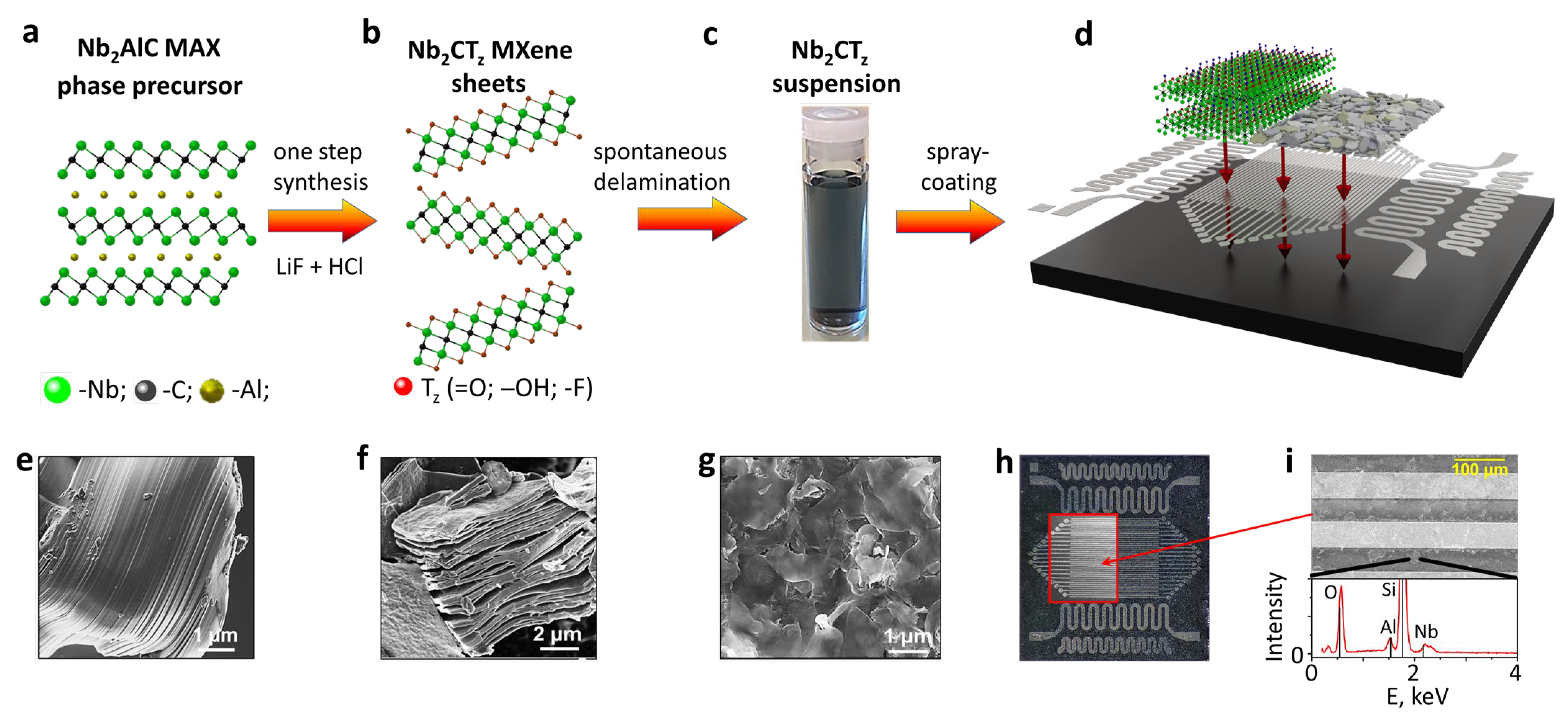
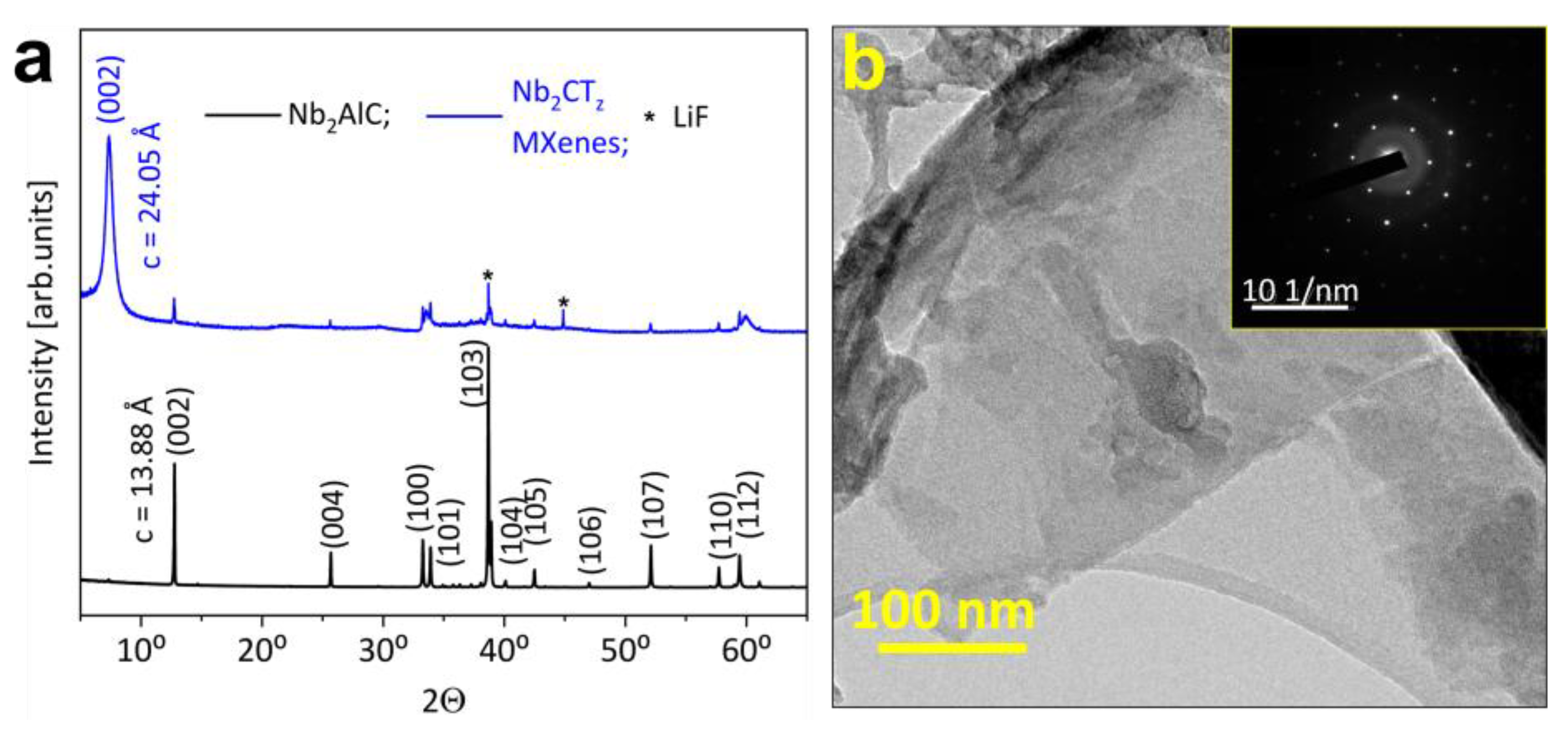
2.1. Synthesis and Characterization of Nb2CTz MXenes

Nb2CTz MXenes were synthesized via a selective chemical etching of Al layers from a bulk Nb2AlC MAX phase precursor in a one-step procedure using a mixture of LiF and HCl according to the protocol reported by J. Xiao et al. [27]. In detail, 2.0 g of LiF was slowly added to 20 mL of 12 M HCl solution and left under constant stirring for 5 min. The vial with the solution was placed in an ice bath where Nb2AlC powder was carefully added in minor portions. After that, the mixture was kept for 90 h at 60 °C under continuous stirring. Following the reaction, the solution was washed multiple times with deionized water, with further centrifugation at 3500 rpm for 5 min until a nearly neutral pH value was obtained. The presence of Li ions in the etching solution allows for a spontaneous Li intercalation between the MXene layers during the etching. This effect favors further delamination of multilayers into single or few-layered sheets using a vortex shaking process. After the vortex shaking, the mixture was centrifuged again until a stable suspension of well-delaminated Nb2CTz sheets appears. This step was repeated several times, and the supernatant was collected over the PVDF membrane through vacuum-assisted filtration to be dried under vacuum, with residual pressure down to approx. 30 mbar, at room temperature (RT).
Scanning electron microscopy (SEM) of the Nb2AlC MAX phase and Nb2CTz MXenes was performed using a FEG ZEISS GeminiSEM 300 instrument (Carl Zeiss AG, Oberkochen, Germany). SEM images of the sensor chip were recorded using an Aspex Explorer microscope (FEI, Delmont, PA, USA) equipped with an energy dispersion X-ray (EDX) detector. X-ray diffraction (XRD) patterns were recorded using a D8 Bruker diffractometer (Bruker, Billerica, MA, USA) operating under the Bragg–Brentano geometry and equipped with a Cu anode providing X-rays with a 1.5418 Å wavelength. Transmission electron microscopy (TEM) images were acquired with an JEOL 2010 microscope (JEOL, Akishima, Japan) at an acceleration voltage of 200 kV. High-resolution X-ray photoelectron spectroscopy (HR-XPS) measurements were performed in the VUV-Photoemission beamline of the Elettra synchrotron facility (Trieste, Italy).
In order to evaluate the thickness of the Nb2CTz layer coated over the chip, we applied a stylus profilometry (stylus profiler Dektak 150, Veeco, Plainview, NY, USA) with a stylus of 2 μm radius under a force equal to 1 mg. The resolution of measuring points was approx. 0.05 μm.

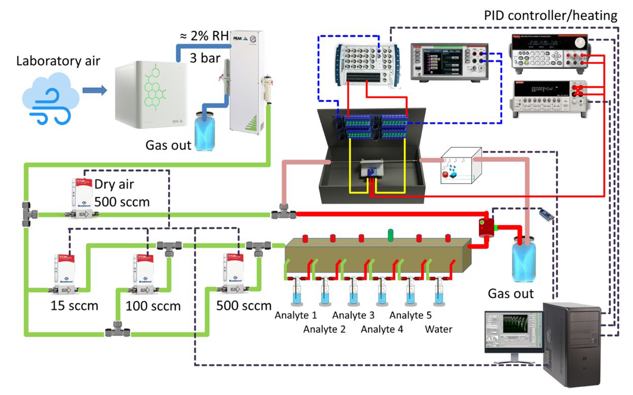
2.2. Gas-Sensing Experiment

To perform gas sensor measurements, we employed the multielectrode chip platform [28]. In brief, the chip is a Si/SiO2 substrate patterned with Pt strip electrodes with 50 µm gaps [29]. To deposit the MXene layer on the chip, a dispersion of delaminated Nb2CTz in isopropanol, 0.1 mg/mL, was sprayed onto a working area of the chip, of 0.215 mm2, using a spray brush system. The distance between the nozzle tip of the airbrush and the multielectrode chip was adjusted to 7 cm. The flow rate of the MXene suspension was optimized to 5 s/drop by changing the position of the airbrush needle. The deposition pressure was adjusted to 1 bar and the deposition temperature to 100 °C. The thickness of the Nb2CTz layer was controlled by the number of deposition cycles.
After the preparation, the chip was connected with Al wires, 38 μm diameter, to a window in the ceramic holder equipped with multiple metallic thin-film roads to contact pads and 50-pin interface (Erni SMC, 1.27 mm, Erni Electronics GmbH, Adelberg, Germany) for connecting the external reading electronic circuits. For analyte gas supply, the Nb2CTz-based chip-in-holder was introduced to an alloy steel-fabricated chamber supplied with two sealing heat-tolerant rubber rings. The chamber was blown with a gas flow via in-mounted tubes, 1/8′ in diameter, to feed the probes primarily to the chip frontside. Figure 1 shows the measuring setup for conducting the gas-sensing measurements with the chip under study. The whole chamber and all the wires were put in a grounded metal box in order to avoid any influence of the external electromagnetic field.
All the electrode pairs in the on-chip sensor array were measured upon applying d.c. electric potential, up to 5 V, in sequence via multiplexing relays (Songle Relay, Ningbo, China) to record the current and derive the resistance of each layer area between electrodes. These resistances, up to 10 GOhm, were processed as sensors of the chemiresistive type. The current was recorded by a multimeter (Keithley DAQ6510, Keithley Instruments, Solon, OH, USA) to be fed via an analog I/O unit (USB-6259, National Instruments Co., Austin, TX, USA) with a rate of up to 300 ms per sensor. Two modes of electrical readings were employed in the course of the study: (i) measuring I(V) dependencies while applying the electric bias in the range of [−5;+5] V mainly in background air conditions to evaluate the contact between the layer under study and electrodes, and (ii) measuring I(t) transients converted to R(t) ones while applying a constant bias of 5 V to see the resistance changes upon exposing to various gas probes. A PC operated with LabView@-based software (LabView Full Development System with Application builder, ver. 2020 SP1, National Instruments Co., Austin, TX, USA) was used for this setup.
The gas-sensing measurements were performed when supplying analyte gases via tubes, 1/4′ diameter, joined by Swagelok fittings (Swagelok Co., Solon, OH, USA) at a flowrate of 400 sccm to be managed by high-precision mass-flow controllers (Bronkhorst, Ruurlo, The Netherlands). Regarding the background air, we employed a lab one to be filtered and dried using a corresponding generator (Purge PG14L, Peak Scientific, Glasgow, UK) purged with a compressor (Precision Compressed Air 230v, Peak Scientific Instruments Ltd., Glasgow, UK) yielding 40 psi pressure to feed the total gas delivery system.
To enrich the air with analyte probes, we used bubblers (Gebr. Rettberg GmbH, Göttingen, Germany) containing liquids of distilled water, various alcohols (methanol, ethanol, isopropanol, butanol) and 25% NH3 solution in water. The saturated vapors of each analyte emitted primarily following the bubbling were diluted by air at necessary ratios to yield analyte probes in concentrations of 50–8000 ppm where the limits were managed by the employed flow controllers and physical properties of the analyte liquids. In the case of measurements in humid air as a background, the dry air was first passed through a water-based bubbler to get containing 25% relative humidity or ca. 10,400 ppm H2O concentration. The analyte gas exposures to the chamber with the installed chip were monitored independently by a commercial semiconductor sensor (MQ3, Winsen Co., Zhengzhou, China). The analytes of each type/concentration were supplied to the chip for 90 min to be further cleared by pure background air, which was dry or humid depending on the targeted experimental conditions, for 180 min at least. The measurements of the chemiresistive response of the Nb2CTx film as a layer in the chip were conducted at a temperature range of 25–300 °C to be maintained by the chip in-built meander heaters. The power dissipated over the heaters was managed by a proportional-integral-derivative (PID) controller accounting for data from local on-chip thermoresistors which were initially calibrated with a high-resolution IR camera (InfRec R500EX-P-D, Nippon Avionics Co., Yokohama, Japan) equipped with a 21 μm close-up lens.

3. Results and Discussion

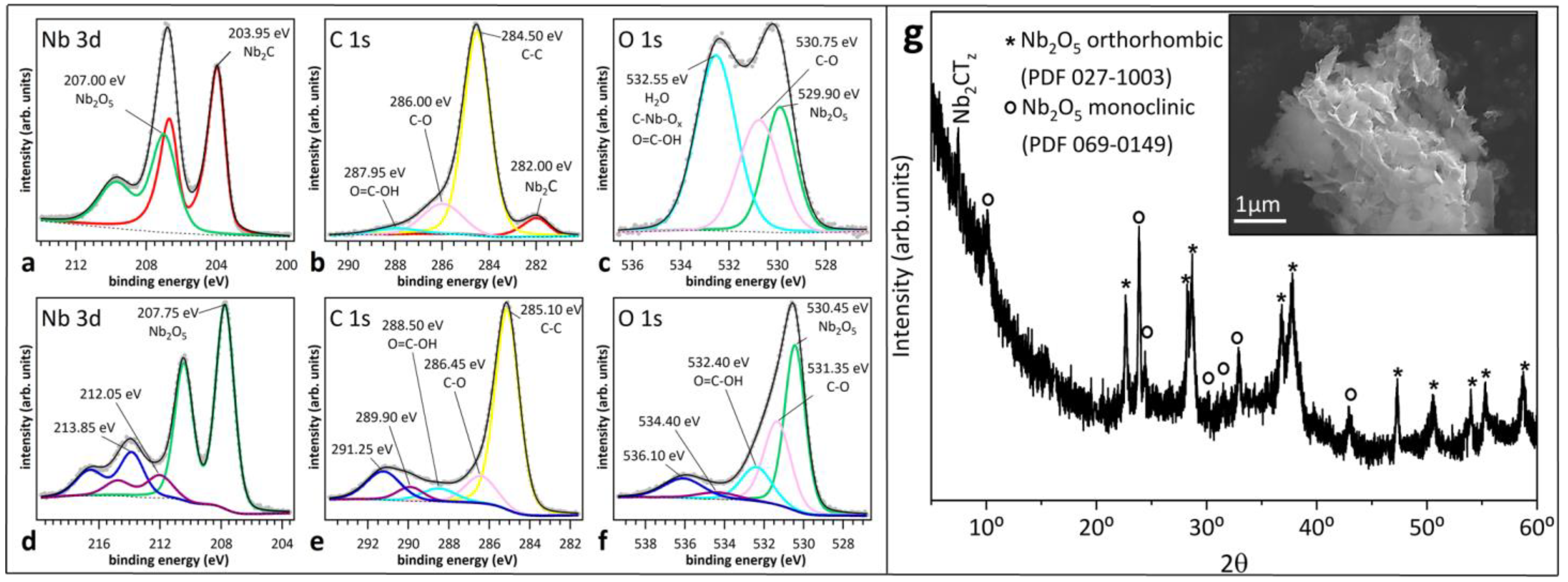
3.1. Synthesis and Characterization of Nb2CTz MXenes

To produce Nb2CTz MXenes, a selective chemical etching of Al layers from bulk Nb2AlC was carried out in a one-step procedure using a mixture of LiF and HCl as detailed in the Section 2. These etchants are widely used for the synthesis of Ti3C2Tx MXenes and allow one to produce large flakes under a mild delamination condition. We have adapted this procedure to obtain Nb2CTz, which is schematically illustrated in Figure 2. The Nb2AlC MAX phase consists of alternating Nb2C and Al layers (Figure 2a) and exhibits a densely packed structure (Figure 2e) as revealed by SEM. After the selective removal of Al, a characteristic accordion-like multilayer structure appears (Figure 2f) due to the release of H2 gas arisen during the reaction of Al and HF. This structure indicates the conversion of the MAX phase to MXenes, which was additionally confirmed by XRD. The synthesis of Nb2CTz under optimized conditions is reproducible to yield MXenes with the same structural characteristics.
The XRD plots given in Figure 3a show that the (002) peak of the parent MAX precursor significantly shifted after the MXene synthesis to the lower 2θ position, which corresponds to a change in the c-parameter from 13.88 Å to 24.05 Å. This is due to an increase in the interplanar spacing as a result of Al etching and subsequent intercalation of water and Li ions.
The XRD pattern of the MXenes also reveals the presence of low-intensity peaks of the initial precursor. However, unreacted MAX phase and non-delaminated MXene multilayers are easily separated from the delaminated suspension.
The presence of Li ions in the etching solution favors a further delamination of multilayers into single or few-layer sheets. After delamination, Nb2CTz suspension exhibits a characteristic light blue color when diluted (Figure 2c) [30]. We drop-cast the delaminated suspension over the Si/SiO2 substrate and observed the poly-flake morphology of the deposited layers using SEM (Figure 2g). It is clearly seen that the film consists of translucent flakes, irregular in shape and of rather large sizes (1–2 µm). From the observation of single MXene flakes in TEM, we notice that Nb2CTz exhibits typical flake features, which are illustrated in Figure 3b, similar to delaminated Ti3C2Tx [26]. The selected area electron diffraction (SAED) pattern of the flakes shows (inset, Figure 3b) the hexagonal arrangement of atoms which retains the symmetry of the parent precursor and confirms the high crystallinity of the produced 2D sheets. It is important to note here that as-prepared pristine Nb2CTz MXenes do not exhibit any oxidation, as evidenced by the absence of oxide peaks in XRD and SAED patterns.
To clarify the physical processes occurring in the Nb2CTz MXene layer under heating, we performed high-resolution X-ray photoelectron spectroscopy (HR-XPS) measurements. The data are summarized in Figure 4: top row spectra refer to as-synthesized Nb2CTz, while bottom row spectra refer to Nb2CTz exposed to 350 °C. Figure 4a reveals the presence of two Nb 3d doublets, which correspond to Nb-C in the MXene (Nb 3d5/2 at 203.95 eV, metallic lineshape) and to Nb2O5 (Nb 3d5/2 at 207.00 eV) that forms spontaneously during the process of exfoliation. In the C1s spectrum, there are four components (Figure 4b). The peak located at 282.00 eV is the counterpart of the Nb-C doublet and has an asymmetric shape, thus confirming the metallic nature of Nb2CTz. The other peaks are assigned to adventitious carbon (284.50 eV), C–O (286.00 eV) and O=C–OH (287.95 eV). The O1s spectrum can be described with three peaks (Figure 4c) corresponding to Nb2O5 (529.9 eV), C–O (530.75 eV) and the convolution of adsorbed water, O-containing termination of MXenes and O=C–OH (532.55 eV).
After exposure of the spray-coated Nb2CTz film to 350 °C, there was no signature of metallic Nb-C bonds either in the Nb 3d spectrum (Figure 4d) or in the C 1s spectrum (Figure 4e). This indicates that Nb2CTz MXenes apparently tend to oxidize faster than Ti3C2Tx due to the presence of two transition metal layers instead of three ones that are in direct contact with air. The Nb 3d spectrum of Figure 4d consists of three doublets (Nb 3d5/2 at 207.75, 212.05 and 213.85 eV) assigned to Nb2O5 oxide. These shifted doublets originate from charging effects of different magnitudes (0.75, 5.05 and 7.85 eV towards higher binding energy with respect to 3d5/2 in Figure 4a) characterizing different parts of the sample. This interpretation is substantiated by the observation of similar shifted components in the C1s and O 1s spectra (Figure 4e,f). The peak of adventitious carbon in Figure 4e is located 0.60 eV deeper than the corresponding peak in Figure 4b. The two features at 289.90 and 291.25 eV are mainly ascribed to adventitious carbon peaks shifted by stronger charging effects. Similarly, the Nb2O5 peak in the O 1s spectrum of Figure 4c is located 0.55 eV deeper than the corresponding peak in Figure 4f. Also, two additional shifted components are observed (534.40 eV and 536.10 eV) in this case [31]. The XRD pattern confirms the absence of Nb2CTz and the coexistence of orthorhombic and monoclinic crystallographic phases of Nb2O5 oxide. The large and phase-dependent bandgap of Nb2O5 (3.1–5.3 eV) can explain the different energy shifts of the photoemission peaks observed in Figure 4d–f. Notably, the SEM image in the inset of Figure 4g shows that the surface of the oxidized sample has a thin flake-like structure that differs from the typical morphology of bulk Nb2O5 particles.

3.2. Gas-Sensing Measurements

To perform gas sensor measurements, we employed the multielectrode chip platform as detailed in the Section 2 [28,29]. While several samples were prepared at different stages of research, here we show the data related to exemplary chip to be fully characterized in order to highlight its major features. The deposited Nb2CTz sheets (Figure 2h,i) cover the working area of the chip in the form of a percolating layer. The profiles of the layer were taken across the electrodes of the chip. The height of the electrodes is approximately 1.5 µm and is shown by the black dashed line in Figure 5. The Nb2CTz layer is lying between and over the top of the electrodes; its height profile is marked in red, orange and green, corresponding to different scans. The layer thickness is estimated as the difference between cross-electrode profiles of the pristine and the coated chip and does not exceed 700 nm in the inter-electrode gaps.
The EDX plot (bottom part of Figure 2h) clearly indicates the presence of Nb from the MXenes, Si and O from the substrate (due to the small thickness of the spray-coated film) and residual traces of Al.
After the chip preparation and its storage under air conditions, the gas-exposure tests at room temperature revealed no changes in the resistance of the Nb2CTz film that went beyond the range of 10 GOhm that could be measured. It would seem that the MXenes were spontaneously oxidized upon deposition, probably in the form of Nb2CTz/Nb2O5 or Nb2O5 phases, resulting in non-measurable conductivities. Therefore, to activate the film conductance, we sequentially heated the chip and could then measure the resistance, still in the GOhm range, at temperatures close to 300 °C. Figure 6a shows I-V curves measured when the chip was exposed to dry air. Although the curves look rather linear, these data indicate the existence of a slight Schottky barrier between the layer and Pt electrode related to differences in the work functions of these materials [32]. When the chip was exposed to test analyte vapors, we could observe a reliable reduction in resistance with a magnitude depending on the analyte concentration. The typical R(t) transient is shown in Figure 6b for the case of methanol vapors mixed with dry air, at a concentration of 100–8000 ppm. For comparison, we show the signal of a commercial semiconductor sensor given as an electric bias, U, in volts to the same exposures. As one can see, resistance of the Nb2CTz film fully follows the varying signal of the commercial sensor although at a lower amplitude change. Similar behavior was observed when the chip was exposed to other test analytes, which is consistent with the chemiresistive effect in n-type wide-band semiconducting oxides [33], which highlights the reducing nature of the test analytes.
The major sensor characteristic, the calibration function of the response, S, versus gas concentration, C, is given in Figure 6c in a double log scale. The response is defined as a relative change in film conductance in percent:
S = G i ( g a s ) G i ( a i r ) 1 × 100 ,
where G i ( g a s ) and G i a i r   are the local conductances of the film located between each couple of electrodes (sensor element) recorded upon an exposure to the analyte gas probe and background air, respectively.
As one can see, all the S(C) curves describing the analytes follow the S ~ C n function to be compatible with the Freundlich adsorption isotherm. The power exponent values related to the analyte probes are listed in Table 1. The lowest value of n, ca. 0.04, is observed for ammonia vapors, which yields a very limited sensor response, down to ca. 1–2%, in contrast to alcohol vapors where n varies between 0.14 and 0.29; still, the response magnitude to alcohols lies in the range of 8–100%. It is interesting that humidity also exhibits a reduced chemiresistive effect with a magnitude of sensor response similar to ammonia, although the n value of 0.16 for this analyte corresponds to those characterizing alcohols.
To further elucidate the effect of H2O vapors, we performed studies exposing the chip to the same analytes mixed with wet air, at 25% RH. These data are summarized in Figure 6d along with data observed in dry background air. As one can see, the presence of H2O in a background atmosphere substantially lowered the sensor response to all the analytes, although the signals are still in the range of 2–11% at a concentration of 2000 ppm. The observed chemiresistive effect is very similar to one reported earlier with non-stoichiometric Nb2O5 oxide [32,34], and it matured due to the presence of defects, primary oxygen vacancies and redox surface reactions. Still, it can be assumed that the possible contribution from the layer/electrode barrier is driven by a similar nature, when the contact potential depends on the same processes that occur with the material under study itself. As shown above, the Nb2CTz film transforms into an oxide phase at temperatures of 300–350 °C. The latter is known to have a strong non-stoichiometry in oxygen, preferentially observed in high-surface-area nanostructured materials [32]. We assume that the Nb2O5 formed as a result of the oxidation of Nb2CTz is non-stoichiometric, since a well-crystalline oxide is formed at a higher temperature of 800 °C [33]. When a non-stoichiometric Nb2O5 film is exposed to wet air (or a humid atmosphere), OH-groups are adsorbed on an oxygen lattice defect, which then reduce the sensor signal from analytes. This non-stoichiometry of the derived quasi-2D Nb2O5 can also explain its higher signal towards alcohols compared to ammonia in accordance with other data reported in [34]. Interestingly, while our previous study showed that Ti3C2Tz MXenes annealed at 350 °C display the highest response towards acetone [26], Nb2CTz MXenes annealed at the same temperature showed the highest response towards ethanol. This indicates that the selectivity of MXenes is highly dependent on transition metals and derived oxides.
Still, the performance of the derived sensor toward ethanol vapors is comparable or exceeds one reported in the literature for the pristine Nb2O5 of various morphologies. We have compared these data in Figure 7.
However, we cannot selectively distinguish the analytes by taking the signal of a single sensor element. Therefore, for the selectivity issue, we could consider the vector signals generated by the whole sensor array located on the chip, regarding all the test analytes recorded in stationary parts of R(t) curves [43]. The multisensory vector signal was processed with the linear discriminant analysis (LDA) algorithm using homemade software. This technique reduces the original multidimensional signal of the array, whose dimensionality is equal to the number of sensors, into an artificial space of features with the dimensionality of (N − 1), where N is the number of classes (here, analytes) to recognize [44,45]. In essence, the LDA processing is performed via maximizing the inter-class variation of vector signals versus their in-class scatter. The vector array data given, for example, in the case of analytes present at a concentration of 2000 ppm, are shown in the LDA space of Figure 6e, where they are grouped according to origin. Here, we display a 2D cross-section of the total 10D LDA coordinate system.
As one can see, the gravity centers of the analyte-related clusters are well distinguished here with an average Mahalonobis distance of 130 units. While the zero point in this space relates to fully noisy data like “white noise” that has no specific features toward the inputs under study, this distance could serve as an indication of selectivity. From the obtained data, it is clear that all the analytes could be distinguished with the developed on-chip array.

4. Conclusions

Thus, the present results show that 2D sheets of Nb2O5, which appeared following the oxidation of Nb2CTz MXenes in the temperature range 300–350 °C, could be beneficial for application in gas sensors to detect alcohol vapors, among which the highest response is observed towards ethanol (~100% at 2000 ppm). The combination of various thorough structural characterizations of the material reveals that the improvement in sensing performance is likely due to the flake-like morphology of the derived Nb2O5 oxide and its non-stoichiometry.
Here, we should note that room-temperature-operated sensors are highly attractive from a power consumption viewpoint. However, in practically all the materials, such an operation appeared mostly in 2D architectonics, which suffers from the long-term impact of adsorbed species. It ordinarily yields a significant shift into the baseline under the high influence of humidity and/or other VOCs and gases present in the normal gas atmosphere. To date, even UV illumination does not give the necessary power to accelerate the rate of adsorption/desorption of gas molecules from the material surface. Therefore, heating remains the “gold standard” for operating chemiresistors as these new data further support.
The reported protocol is easily applied for developing multisensor arrays of the planar type for Enose fabrication with a high sensitivity towards alcohols mixed with dry and wet air in concentrations corresponding to known detection requirements like the regulations by the U.S. Occupational Safety and Health Administration (OSHA). Therefore, it could be considered for various applications including the Internet of Things.

Author Contributions

Conceptualization, H.P. and V.V.S.; methodology, A.A. and S.P.; formal analysis, I.A.P., P.M.S., A.S.V., P.M., K.B.K. and A.V.G.; investigation, H.P., I.A.P., L.R., A.S.V. and K.B.K.; writing—original draft preparation, H.P., P.M., T.O. and V.V.S.; writing—review and editing, H.P. and V.V.S. All authors have read and agreed to the published version of the manuscript.

Funding

I.A.P., A.S.V. and V.V.S. thank the Russian Science Foundation, project no. 22-29-00793. The authors acknowledge Elettra Sincrotrone Trieste for providing access to its synchrotron radiation facilities and for financial support under the IUS internal project (proposal nr. 20220537). P.M.S. and P.M. acknowledge the partial support through the project EUROFEL-ROADMAP ESFRI of the Italian MUR.

Institutional Review Board Statement

Not applicable.

Informed Consent Statement

Not applicable.

Data Availability Statement

Data are contained within the article.

Conflicts of Interest

The authors declare no conflict of interest.

References

  1. Clean air for a sustainable world. Nat. Commun. 2021, 12, 5824. [CrossRef] [PubMed]
  2. Traphagen, N.; Tian, W.; Allen-Gipson, D. Chronic ethanol exposure: Pathogenesis of pulmonary disease and dysfunction. Biomolecules 2015, 5, 2840–2853. [Google Scholar] [CrossRef] [PubMed]
  3. Bartolomé, J.; Taeño, M.; Martínez-Casado, R.; Maestre, D.; Cremades, A. Ethanol gas sensing mechanisms of p-type NiO at room temperature. Appl. Surf. Sci. 2022, 579, 152134. [Google Scholar] [CrossRef]
  4. Jiang, B.; Lu, J.; Han, W.; Sun, Y.; Wang, Y.; Cheng, P.; Zhang, H.; Wang, C.; Lu, G. Hierarchical mesoporous zinc oxide microspheres for ethanol gas sensor. Sens. Actuators B Chem. 2022, 357, 131333. [Google Scholar] [CrossRef]
  5. Wang, R.-H.; Wen, W.; Zheng, S.; Ye, Z.; Wu, J.-M. Layered mesoporous SnO2 for effective ethanol detection at reduced working temperature. Sens. Actuators B Chem. 2022, 362, 131805. [Google Scholar] [CrossRef]
  6. Spagnoli, E.; Krik, S.; Fabbri, B.; Valt, M.; Ardit, M.; Gaiardo, A.; Vanzetti, L.; Della Ciana, M.; Cristino, V.; Vola, G.; et al. Development and characterization of WO3 nanoflakes for selective ethanol sensing. Sens. Actuators B Chem. 2021, 347, 130593. [Google Scholar] [CrossRef]
  7. Yuan, Z.; Yang, C.; Meng, F. Strategies for improving the sensing performance of semiconductor gas sensors for high-performance formaldehyde detection: A review. Chemosensors 2021, 9, 179. [Google Scholar] [CrossRef]
  8. Li, A.; Zeng, W.; Li, Y. NiO-based gas sensors for ethanol detection: Recent progress. J. Sens. 2022, 2022, 1855493. [Google Scholar] [CrossRef]
  9. 2D materials, a matter for chemists. Nat. Nanotechnol. 2023, 18, 535. [CrossRef]
  10. Benchakar, M.; Loupias, L.; Garnero, C.; Bilyk, T.; Morais, C.; Canaff, C.; Guignard, N.; Morisset, S.; Pazniak, H.; Hurand, S.; et al. One MAX phase, different MXenes: A guideline to understand the crucial role of etching conditions on Ti3C2Tx surface chemistry. Appl. Surf. Sci. 2020, 530, 147209. [Google Scholar] [CrossRef]
  11. Li, Y.; Shao, H.; Lin, Z.; Lu, J.; Liu, L.; Duployer, B.; Persson, P.O.Å.; Eklund, P.; Hultman, L.; Li, M.; et al. A general Lewis acidic etching route for preparing MXenes with enhanced electrochemical performance in non-aqueous electrolyte. Nat. Mater. 2020, 19, 894–899. [Google Scholar] [CrossRef] [PubMed]
  12. Anasori, B.; Gogotsi, Y. The rise of MXenes. ACS Nano 2019, 13, 8491–8494. [Google Scholar] [CrossRef]
  13. Wu, M.; He, M.; Hu, Q.; Wu, Q.; Sun, G.; Xie, L.; Zhang, Z.; Zhu, Z.; Zhou, A. Ti3C2 MXene-based sensors with high selectivity for NH3 detection at room temperature. ACS Sens. 2019, 4, 2763–2770. [Google Scholar] [CrossRef] [PubMed]
  14. Sardana, S.; Kaur, H.; Arora, B.; Aswal, D.K.; Mahajan, A. Self-powered monitoring of ammonia using an MXene/TiO2/cellulose nanofiber heterojunction-based sensor driven by an electrospun triboelectric nanogenerator. ACS Sens. 2022, 7, 312–321. [Google Scholar] [CrossRef] [PubMed]
  15. Lee, E.; VahidMohammadi, V.; Yoon, Y.S.; Beidaghi, M.; Kim, D.-J. Two-dimensional vanadium carbide for gas sensors with ultrahigh sensitivity toward nonpolar gases. ACS Sens. 2019, 4, 1603–1611. [Google Scholar] [CrossRef] [PubMed]
  16. Pazniak, H.; Varezhnikov, A.S.; Kolosov, D.A.; Plugin, I.A.; Di Vito, A.; Glukhova, O.E.; Sheverdyaeva, P.M.; Spasova, M.; Kaikov, I.; Kolesnikov, E.A.; et al. 2D molybdenum carbide MXenes for enhanced selective detection of humidity in air. Adv. Mater. 2021, 33, 2104878. [Google Scholar] [CrossRef] [PubMed]
  17. Simonenko, E.P.; Simonenko, N.P.; Mokrushin, A.S.; Simonenko, T.L.; Gorobtsov, P.Y.; Nagornov, I.A.; Korotcenkov, G.; Sysoev, V.V.; Kuznetsov, N.T. Application of titanium carbide MXenes in chemiresistive gas sensors. Nanomaterials 2023, 13, 850. [Google Scholar] [CrossRef]
  18. Khan, K.; Tareen, A.K.; Iqbal, M.; Ye, Z.; Xie, Z.; Mahmood, A.; Mahmood, N.; Zhang, H. Recent progress in emerging novel MXenes based materials and their fascinating sensing applications. Small 2023, 19, 2206147. [Google Scholar] [CrossRef]
  19. Kamysbayev, V.; Filatov, A.S.; Hu, H.; Rui, X.; Lagunas, F.; Wang, D.; Klie, R.F.; Talapin, D.V. Covalent surface modifications and superconductivity of two-dimensional metal carbide MXenes. Science 2020, 369, 979–983. [Google Scholar] [CrossRef]
  20. Zhang, W.; Jin, H.; Zhang, J. Nb2CTx MXene as high-performance energy storage material with Na, K, and liquid K-Na alloy anodes. Langmuir 2021, 37, 1102–1109. [Google Scholar] [CrossRef]
  21. Soleymaniha, M.; Shahbazi, M.-A.; Rafieerad, A.R.; Maleki, A.; Amiri, A. Promoting role of MXene nanosheets in biomedical sciences: Therapeutic and biosensing innovations. Adv. Healthc. Mater. 2019, 8, 1801137. [Google Scholar] [CrossRef] [PubMed]
  22. Li, G.; Singh, R.; Guo, J.; Zhang, B.; Kumar, S. Nb2CTx MXene-assisted double S-tapered fiber-based LSPR sensor with improved features for tyramine detection. Appl. Phys. Lett. 2023, 122, 083701. [Google Scholar] [CrossRef]
  23. Bi, M.; Miao, Y.; Li, W.; Yao, J. Niobium carbide MXene-optics fiber-sensor for high sensitivity humidity detection. Appl. Phys. Lett. 2022, 120, 021103. [Google Scholar] [CrossRef]
  24. Kumar, A.N.; Pal, K. Amine-functionalized stable Nb2CTx MXene toward room temperature ultrasensitive NO2 gas sensor. Mater. Adv. 2022, 3, 5151–5162. [Google Scholar] [CrossRef]
  25. Wang, S.; Liu, B.; Duan, Z.; Zhao, Q.; Zhang, Y.; Xie, G.; Jiang, Y.; Li, S.; Tai, H. PANI nanofibers-supported Nb2CTx nanosheets-enabled selective NH3 detection driven by TENG at room temperature. Sens. Actuators B Chem. 2021, 327, 128923. [Google Scholar] [CrossRef]
  26. Pazniak, H.; Plugin, I.A.; Loes, M.J.; Inerbaev, T.M.; Burmistrov, I.N.; Gorshenkov, M.; Polcak, J.; Varezhnikov, A.S.; Sommer, M.; Kuznetsov, D.V.; et al. Partially oxidized Ti3C2Tx MXenes for fast and selective detection of organic vapors at part-per-million concentrations. ACS Appl. Nano Mater. 2020, 3, 3195–3204. [Google Scholar] [CrossRef]
  27. Xiao, J.; Zhao, J.; Ma, X.; Li, L.; Su, H.; Zhang, X.; Gao, H. One-step synthesis Nb2CTx MXene with excellent lithium-ion storage capacity. J. Alloys Compd. 2021, 889, 161542. [Google Scholar] [CrossRef]
  28. Sysoev, V.V.; Strelcov, E.; Kar, S.; Kolmakov, A. The electrical characterization of a multi-electrode odor detection sensor array based on the single SnO2 nanowire. Thin Solid Films 2011, 520, 898–903. [Google Scholar] [CrossRef]
  29. Rabchinskii, M.K.; Sysoev, V.V.; Glukhova, O.E.; Brzhezinskaya, M.; Stolyarova, D.Y.; Varezhnikov, A.S.; Solomatin, M.A.; Barkov, P.V.; Kirilenko, D.A.; Pavlov, S.I.; et al. Guiding graphene derivatization for the on-chip multisensor arrays: From the synthesis to the theoretical background. Adv. Mater. Technol. 2022, 7, 2101250. [Google Scholar] [CrossRef]
  30. Zhang, D.; Shah, D.; Boltasseva, A.; Gogotsi, Y. MXenes for photonics. ACS Photonics 2022, 9, 1108–1116. [Google Scholar] [CrossRef]
  31. Rani, R.A.; Zoolfakar, A.S.; O’Mullane, A.P.; Austin, M.W.; Kalantar-Zadeh, K.J. Thin films and nanostructures of niobium pentoxide. J. Mater. Chem. A 2014, 2, 15683–15703. [Google Scholar] [CrossRef]
  32. Kreissl, H.T.; Li, M.M.J.; Peng, Y.-K.; Nakagawa, K.; Hooper, T.J.N.; Hanna, J.V.; Shepherd, A.; Wu, T.-S.; Soo, Y.-L.; Tsang, S.C.E. Structural studies of bulk to nanosize niobium oxides with correlation to their acidity. J. Am. Chem. Soc. 2017, 139, 12670–12680. [Google Scholar] [CrossRef] [PubMed]
  33. Qui, L.; Liu, Y.; Xu, S.; Wang, S.; Sun, X.; Zhu, S.; Hou, L.; Yuan, C. In-plane assembled single-crystalline T-Nb2O5 nanorods derived from few-layered Nb2CTx MXene nanosheets for advanced Li-ion capacitors. Small Methods 2020, 4, 2000630. [Google Scholar] [CrossRef]
  34. Mokrushin, A.S.; Simonenko, T.L.; Simonenko, N.P.; Gorobtsov, P.Y.; Kadyrov, N.S.; Simonenko, E.P.; Sevastyanov, V.G.; Kuznetsov, N.T. Chemoresistive gas-sensing properties of highly dispersed Nb2O5 obtained by programmable precipitation. J. Alloys Compd. 2021, 868, 159090. [Google Scholar] [CrossRef]
  35. Zou, Y.; He, J.; Hu, Y.; Huang, R.; Wang, Z.; Gu, Q. Room-temperature hydrogen sensing performance of Nb2O5 nanorod arrays. RSC Adv. 2018, 8, 16897–16901. [Google Scholar] [CrossRef] [PubMed]
  36. Yang, P.; Fan, Y.; Hu, K.; Jiang, L.; Tan, L.; Wang, Z.; Li, A.; Yang, S.; Hu, Y.; Gu, H. Fast, sensitive, and highly selective room-temperature hydrogen sensing of defect-rich orthorhombic Nb2O5-x nanobelts with an abnormal p-type sensor response. ACS Appl. Mater. Interfaces 2022, 14, 25937–25948. [Google Scholar] [CrossRef] [PubMed]
  37. Park, S.; Kim, S.; Park, S.; Hyun, S.-K.; Lee, W.I.; Lee, C. Enhanced ethanol sensing performances of multiple networked Nb2O5 nanorod sensors functionalized with Pd and Au nanoparticles. Nano 2014, 9, 1450098. [Google Scholar] [CrossRef]
  38. Wang, Y.-D.; Yang, L.-F.; Zhou, Z.-L.; Li, Y.-F.; Wu, X.-H. Effects of calcining temperature on lattice constants and gas-sensing properties of Nb2O5. Mater. Lett. 2001, 49, 277–281. [Google Scholar] [CrossRef]
  39. Mozalev, A.; Bendova, M.; Vazquez, R.M.; Pytlicek, Z.; Llobet, E.; Hubalek, J. Formation and gas-sensing properties of a porous-alumina-assisted 3-D niobium-oxide nanofilm. Sens. Actuators B Chem. 2016, 229, 587–598. [Google Scholar] [CrossRef]
  40. Gullino, A.; Parvis, M.; Lombardo, L.; Grassini, S.; Donato, N.; Moulaee, K.; Neri, G. Employment of Nb2O5 thin-films for ethanol sensing. In Proceedings of the I2MTC 2020—International Instrumentation and Measurement Technology Conference, Dubrovnik, Croatia, 25–28 May 2020; p. 9128457. [Google Scholar] [CrossRef]
  41. Lombardo, L.; Grassini, S.; Parvis, M.; Donato, N.; Gullino, A. Ethanol breath measuring system. In Proceedings of the MeMeA 2020—Conference Proceedings, Bari, Italy, 1 June–1 July 2020; p. 9137215. [Google Scholar] [CrossRef]
  42. Kadir, R.A.; Rani, R.A.; Zoolfakar, A.S.; Ou, J.Z.; Shafiei, M.; Wlodarski, W.; Kalantar-Zadeh, K. Nb2O5 Schottky based ethanol vapour sensors: Effect of metallic catalysts. Sens. Actuators B Chem. 2014, 202, 74–82. [Google Scholar] [CrossRef]
  43. Sysoev, V.V.; Strelcov, E.; Kolmakov, A. Multisensor micro-arrays based on metal oxide nanowires for electronic nose applications. In Metal Oxide Nanomaterials for Chemical Sensors; Springer: New York, NY, USA, 2013; pp. 465–502. [Google Scholar] [CrossRef]
  44. Hierlemann, A.; Gutierrez-Osuna, R. Higher-order chemical sensing. Chem. Rev. 2008, 108, 563–613. [Google Scholar] [CrossRef] [PubMed]
  45. Sysoev, V.V.; Kiselev, I.; Trouillet, V.; Bruns, M. Enhancing the gas selectivity of single-crystal SnO2:Pt thin-film chemiresistor microarray by SiO2 membrane coating. Sens. Actuators B Chem. 2013, 185, 59–69. [Google Scholar] [CrossRef]
Figure 1. The experimental setup to measure the response of the Nb2CTz MXene-based chip to various analyte gases emitted via bubbling. The tube lines containing a background air and analyte-enriched air are marked by light green and red, correspondingly.
Sensors 24 00038 g001
Figure 2. Schematic depiction of Nb2CTz MXene synthesis and the Nb2CTz-based multielectrode chip: (a) structure of the Nb2AlC MAX phase precursor; (b) structure of Nb2CTz sheets produced via a selective chemical etching of the Al layer in the mixture of LiF and HCl; (c) photo of the delaminated suspension of Nb2CTz MXenes; (d) cartoon of the chip fabrication; (eg) SEM images of MAX precursor (e), multilayered MXenes (f) and delaminated Nb2CTz sheets in the layer (g); optical and SEM images of the chip covered by Nb2CTz layer via a spray casting and EDX spectrum taken in the inter-electrode gap (h,i).
Sensors 24 00038 g002
Figure 3. Structural characterization of Nb2CTz MXenes. (a) XRD patterns of Nb2AlC MAX phase precursor and derived Nb2CTz MXenes by the chemical etching of Nb2AlC; (b) TEM image of Nb2CTz flakes with corresponding SAED pattern (inset).
Sensors 24 00038 g003
Figure 4. HR-XPS data of as-prepared Nb2CTz MXenes (ac) and after oxidation at 350 °C (df). XRD pattern and SEM image (inset) for the oxidized Nb2CTz MXenes (g).
Sensors 24 00038 g004
Figure 5. The stylus profile scans taken over the multielectrode chip coated with an oxidized Nb2CTz MXene layer following gas-sensor measurements at high temperatures. The spot of four electrodes, #7–10 counting from left to right in the chip, is taken for example.
Sensors 24 00038 g005
Figure 6. Gas-sensing performance of the Nb2CTz/Nb2O5-based chip at 300 °C: (a) I-V curves measured in dry air for three sensor elements; (b) typical R(t) transient of single sensor element (top) and voltage signal of commercial sensor exposed to methanol vapors; (c) the chemiresistive response of the sensor elements toward various analyte concentrations; (d) selectivity diagram of chemiresistive response at an analyte concentration equal to 2000 ppm; (e) 3D cross-section of the total 10D LDA space; the points relate to chip vector signals to analytes, 2000 ppm concentration, ellipses frame areas for vector data scattered under Gaussian distribution with 0.9 confidence around gravity centers of analyte-related clusters; abbreviations: Amm—ammonia; Iso—isopropanol; But—butanol; Meth—methanol; Eth—ethanol; Hum—humidity.
Sensors 24 00038 g006
Figure 7. A comparative plot of sensor performance of pristine Nb2O5 structures versus ethanol vapors based on literature data (adapted from Refs. [35,36,37,38,39,40,41,42]) regarding the results presented here. S/C is the response (S)-to-concentration (C) ratio.
Sensors 24 00038 g007
Table 1. The power index, n, of the S(C) curve characterizing the gas response of sensor elements of the Nb2CTz/Nb2O5-based chip operating at 300 °C versus various test analytes.
GasAmmoniaHumidityIsopropanolButanolMethanolEthanol
n0.04 ± 0.020.16 ± 0.020.15 ± 0.030.14 ± 0.040.29 ± 0.060.15 ± 0.03
Disclaimer/Publisher’s Note: The statements, opinions and data contained in all publications are solely those of the individual author(s) and contributor(s) and not of MDPI and/or the editor(s). MDPI and/or the editor(s) disclaim responsibility for any injury to people or property resulting from any ideas, methods, instructions or products referred to in the content.

