
Forgotten Italian CPU – The Genesys B52 MMX
Introduction
 On this site you can read about thousands of processors models. And every year it is more and more difficult to write about some new (old) processors, since everything has been known for a long time. But there are also exceptions to the rule which we love to find. In 2021, I learned about one unusual processor, the information about which I want to share with you. The roots of this processor’s history go back to Italy, in the distant year or 1998. This time just falls on the confrontation between Intel and its second generation Pentium and AMD K6-2 and K6-3 processors. The Cyrix MII processors from Cyrix Corporation, IDT WinChip 2s and Rise mP6s were still going strong as well.
But before we talk about the Genesys B52 MMX processor, we should take a closer look at Intel Pentium II processors in general, as the Italian processor primarily owes its appearance to them.
Intel Pentium II
 From 1993 to 1997, the Pentium dominated all market segments. Over time, the name of the “Pentium” trademark even grew into a household name (Its all about the Pentiums baby), but with the release of the Pentium II, everything changed. If earlier Intel did not deeply segment the market, there were Pentium Pros for workstations and servers, and for everything else there were various models of Intel Pentium processors, in which, at the end of their domination, Intel added MMX instructions, depriving and thereby putting an end to its server segment. The new slot form factor of the processor, the abandonment of the usual pins and ceramics and further segmentation of the market (using Intel Celeron processors and the new Xeon line) radically changed the further course of development of the history of microprocessors.
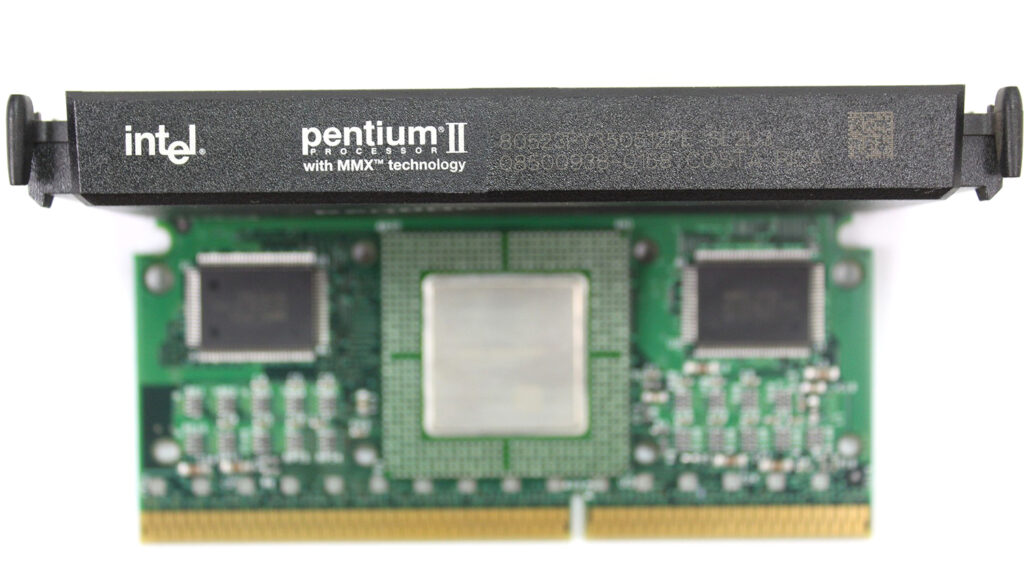
![]() May 7, 1997 saw the light of the first models of Intel Pentium II processors, manufactured on a 350nm process with a core voltage of 2.8 volts. The first models were based on the Klamath core (named after the river by which The CPU Shack is located) core, operating at 233 and 266 MHz. The main differences from the Pentium Pro predecessor it was based on were the L1 cache increased from 16 to 32 Kb, and the presence of a block of SIMD instructions called MMX first introduced on the last P55C processors. Like the Pentium Pro it featured its own L2 cache on the module, but in this case it was 512KB fixed on the same PCB as the processor core, a much cheaper solution then the dual ceramic cavity package of the Pentium Pro.
May 7, 1997 saw the light of the first models of Intel Pentium II processors, manufactured on a 350nm process with a core voltage of 2.8 volts. The first models were based on the Klamath core (named after the river by which The CPU Shack is located) core, operating at 233 and 266 MHz. The main differences from the Pentium Pro predecessor it was based on were the L1 cache increased from 16 to 32 Kb, and the presence of a block of SIMD instructions called MMX first introduced on the last P55C processors. Like the Pentium Pro it featured its own L2 cache on the module, but in this case it was 512KB fixed on the same PCB as the processor core, a much cheaper solution then the dual ceramic cavity package of the Pentium Pro.
Before the Pentium II, only the Pentium Pro could boast of its own cache, running at the frequency of the CPU core. But, placing the CPU core and L2 cache on the same substrate was an expensive pleasure even for Intel, and the processors had to be cheaper for better competition, which was getting more and more intense. Intel then made a “wise” decision, as a result of which the Pentium II got a its own L2 cache next to the CPU core This engineering solution significantly reduced the cost of manufacturing processors. BSRAM L2 cache chips were manufactured by Toshiba, SEC and NEC at that time, rather then being made in house by Intel, further easing the cost burdens.
Pentium II Klamath SECC1 PBGA Core 2 x Cache on front 2x + TAG on back
For all models of Pentium II processors, the cache size remained unchanged and equaled 512 KB, while different Pentium Pro models had a cache from 256 to 1024 KB. The L2 cache of the first Pentium II processors consisted of four microcircuits located on both sides of the cartridge processor board and operated at half the core frequency. In addition to the processor core and 4 L2 cache chips, there was also a tag-RAM chip on the cartridge PCB, a total of 6 IC’s.
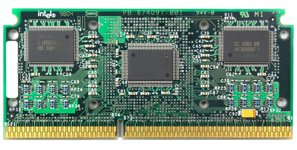
Backside with 2x cache + TAG
The tag-RAM size/configuration determines which range of main memory can be cached. For example, if the L2 cache is 256 KB and the tag RAM is 8 bits wide, then this is enough to cache up to 64 MB of main RAM. However, if you add additional RAM in the process, it will not be cached unless you also expand the tag RAM. On Socket 1-3 486 systems, most motherboards allowed adding and modifying additional L2 cache and tag-RAM chips for this purpose. The Pentium Pro had built-in L2 cache and tags capable of caching up to 4GB of main memory, whereas the first Pentium IIs could cache up to 512MB of RAM. This was in part to set them apart from the server oriented Pentium II Xeon which had full speed cache capable of caching 4GB (or 64GB with PSE-36),
 In January 1998, Intel announced the Pentium II processor, built on a new core, codenamed Deschutes (Another river in Oregon). The processor core was manufactured using the smaller 250nm process, which lowered the operating voltage to 2.0 V, instead of 2.8 V for “Klamath”. The L2 cache of 512 KB still worked at half the core frequency, but it was made in the form of two BSRAM chips located to the side of the processor package. In later modifications of the Pentium II Deschutes core, Intel replaced the tag-RAM chip, thanks to which the processors could cache up to 4 GB of RAM (the 82459AD revision).
The first generation of Intel Celeron processors were based on the “Covington” core were essentially processors on the “Deschutes” core, but without ANY L2 cache. Thanks to this, they had very poor performance, but they overclocked very well, demonstrating the best overclocking figures up to double the nominal clock frequency.
Deschutes core with Organic BGA core and 2x cache chips on front. TAG on back
 All overclocking of Pentium II, as a rule, rested on the characteristics of microcircuits used by BSRAM and tag-RAMs. The latter, like the cache, was much disliked voltage rises, and with inept handling, an expensive Pentium II could turn out to be a Celeron “Covington”, if such microcircuits failed.By the way, they warmed up decently on Pentium II processors based on the “Klamath” core so cooling was very important as well. The multiplier in 99% of Pentium II processors was locked (very early production ones were unlocked and Engineering Samples of course), so overclocking was performed by raising the FSB frequency, this being dependent always on the cache and TAG chips installed in that particular processor.
A simple example. In Costa Rica, where Intel has an advanced advanced processor assembly/test factory, which simultaneously assembled high-frequency models with 450 and 300 megahertz. The cartridge and core for these processors are identical (and the multiplier was the same 4.5x as well 66×4.5 for the 300 and 100×4.5 for the 450). The difference was only in the installed cache memory with different speed rating in nanoseconds. Sometimes on the assembly line there was only a fast cache memory capable of operating at a frequency of 225 MHz, intended for models of processors with 450 MHz. In this case, it was also installed on the model with a frequency of 300 MHz, as a result of which they overclocked perfectly.
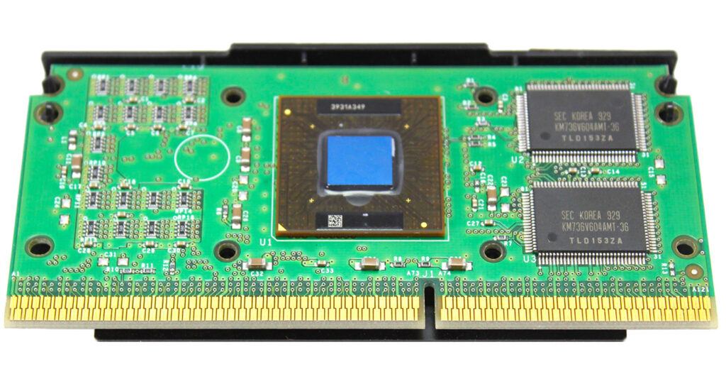
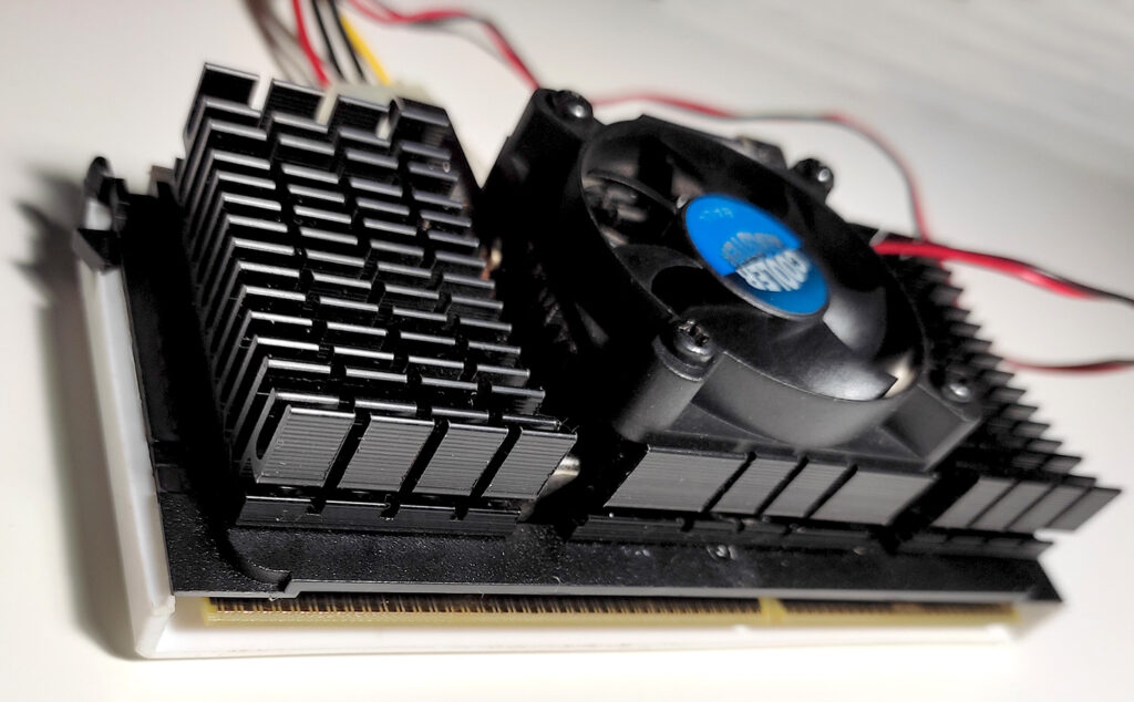
Genesys B52 MMX CPU
The history of the Italian processor began in the city of Monopoli, in the province of Bari in Italy. In 1998, Italian Marcello Console founded Genesys, which initially employed 10 people. The main idea of the Genesys business was the production of modified Intel Pentium II processors based on the “Deschutes” core, at a much lower price than the Pentium II ones of similar clock speed. Plus a warranty period extended to 3 years and productivity increased by 5% or more. It turns out to be a solid Attraction of Generosity!
Genesys had registered its own domain www.b52mmx.com and is getting ready to implement their processors in ready-made system units. Unfortunately, nothing is known about the manufacturing process, it remains a mystery to this day. There is not so much information on these processors, but let’s try to figure out what these processors were.
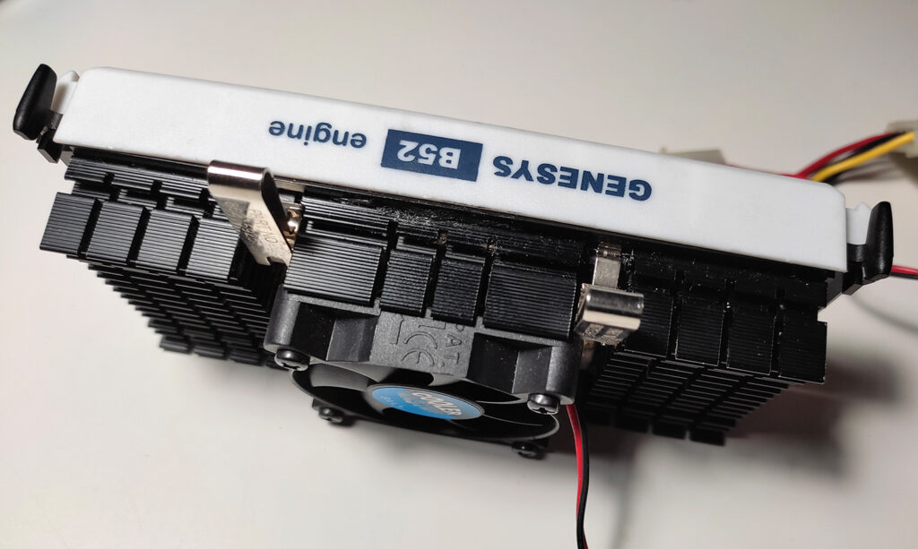
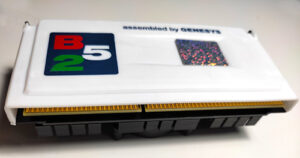
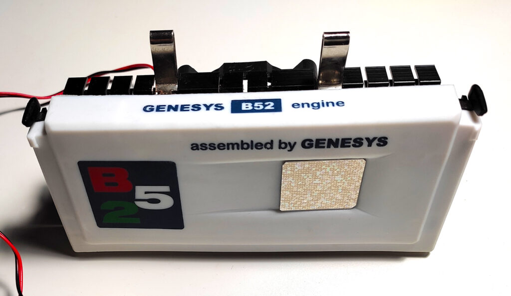
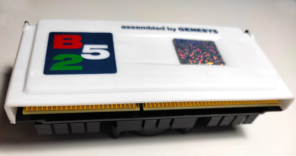
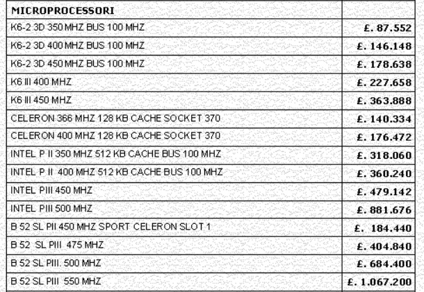
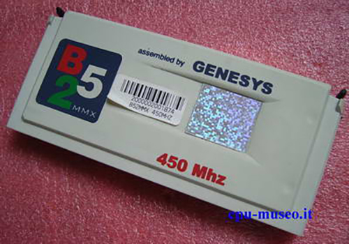
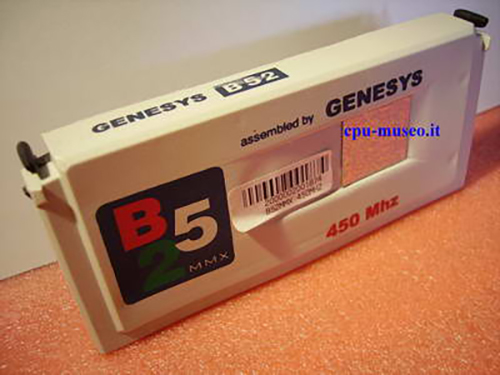
There were four Genesys B52 MMX models with clock frequencies: 300, 350, 400 and 450 MHz. There is information that the first models were manufactured using 350 nm technology, and the rest – at 250 nm. The processors cost about 25% less than similar Intel processors, the warranty period was extended from two to three years. The cost of the Genesys B52 processor with a frequency of 450 MHz was then 750,000 lire, or about $450 (1998 Dollars) which made it about $220USD cheaper than a Pentium II 450 MHz ($669 at introduction). The appearance of the processor is most striking. The white cartridge, after the usual black, looks clearly unusual and makes the processor even more mysterious.
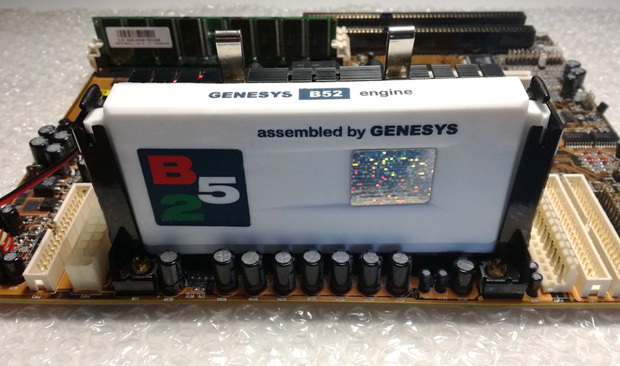
On the front panel in multicolored letters in a blue square there is a kind of “B52” logo of the processor model and the inscription “assembled by GENESYS”. The colors of the logo, Red White and Green, are the colors of the Italian Flag. There is information on the network that the name of the model comes from the name of the American strategic bomber – B-52 Stratofortress, a Boeing plane that has been in service with the US Air Force since 1955 (and will be till around 2075).

B-52 Flying with Italian Fighters off the coast of Italy.
One of the modifications of the B-52 is the absolute record holder for range among combat aircraft. It is also one of the few military aircraft in continuous service for over half a century (an will be for a century). Despite the fact that the B-52 was developed in the late 1940s and early 1950s, it remains the main aircraft of the long-range bomber aircraft of the American Air Force and will remain for many years to come.
There is one more inscription “GENESYS B52 engine” on the upper end of the processor and no more information. One reviewer of that time got this processor and this is what he then noted:
The internal structure of the B52MMX-450 exactly corresponds to that of the Pentium-II-300 from the SL2W8 series, but the location and values of some resistors have been changed.
Genesys apparently bought 300 MHz processors from Intel, replaced the module case, did some additional work, and then sold the product as a 450 MHz processor. This explains the lower price for the B52 MMX processor. This was doable because they used the same 4.5X multiplier. All Genesys had to do is improve the cooling and raise the FSB from 66MHz to 100MHz. This was similar to their other ‘models’ For example the 350MHz likely started out as a 3.5 x 66MHz 233MHz Part, raise the FSB to 100 and you have a 350MHz part (though that may have been a stretch for your avg 233 PII)
Genesys wrote in the instruction manual that the user should manually set the system bus frequency to 100 MHz and set the multiplier equal to x4.5. The processor cartridge houses two L2 cache chips from NEC with a speed of 5 ns. The original Intel Pentium-II 450 MHz processor has faster cache memory chips with a speed of 4.4 ns. The tests carried out at that time showed amazing results: the L2 cache of the B52MMX was faster, the data transfer rate was at 419 MB/s, while the Intel Pentium-II 450 MHz had only 378 MB/s. So there was a bit more then simple overclocking going on here.
A second reviewer did a more detailed comparison of the Genesys B52MMX 450 MHz processor and highlighted the following key features:
1. The rear aluminum plate B52MMX, which is in direct contact with the heatsink, is absolutely smooth and the same as that of the Pentium II at 233 and 333 MHz. Whereas the original Pentium II 450 MHz has a kind of protrusion at the point where the L2 cache meets the aluminum itself; besides, the lower part is made of plastic for the B52MMX, and of steel for the Pentium II 450 MHz.
2. B52MMX L2 cache chips belong to the NEC and have an output of 5 ns (full part #- NEC Japan D432836LGF-A50 9832E7013). The Tag-Ram chip located on the back of the cartridge is labeled S82459AD 88300089 SL2WF. Comparing this information, it turns out that the Tag-Ram chip is identical to that used in the original Pentium II 400 MHz processors.
But then the authors of the review got confused with the conclusions. They considered the B52MMX to be some kind of mix of an Intel Celeron processor on the Mendocino core with disabled L2 cache (128 KB) and added 512 KB L2 cache from NEC. In fact, the differences lie in the different packaging options for the SECC and SECC2 cartridge of different Pentium II models. (the Celeron used a PBGA type chip for the processor, as did some Pentiums IIs before switching to a smaller Organic BGA style chip) The review has not disappeared yet and is available at this link (https://www.hwupgrade.it/articoli/cpu/151/b52mmx_index.html). But their testing figures turned out to be interesting.
The B52MMX had better L2 cache speed at the same 450 MHz clock speed. Around 9% faster is a big deal
| Intel Pentium II 450 Mhz | 359.4MB/s |
| Genesys B52MMX 450 Mhz | 394.7MB/s |
Next, a system was assembled based on the Abit BH6 motherboard (i440BX chipset) and both processors were tested in the Ziff Davis Cpu Mark 32 test suite:
| Intel Pentium II 450 Mhz (100×4.5) | 1130 |
| Genesys B52MMX 450 Mhz (100×4.5) | 1160 |
| Intel Pentium II 504 Mhz (112×4.5) | 1260 |
| Genesys B52MMX 504 Mhz (112×4.5) | 1300 |
As you can see from the table, the Genesys B52MMX processor surpasses the stock 450, Intel clearly did not expect such a turn of events. Remember Genesys’s promise of a ‘5% increase in productivity’? It would seem that this is what they were referring to. Not only were you getting a faster processor for cheaper, you were getting a FASTER processor then what you would from Intel. On the site www.b52mmx.com potential buyers could familiarize themselves with the configurations of system units with snow-white processors. Thanks to the web archive, we have now managed to see what these proposals looked like then.
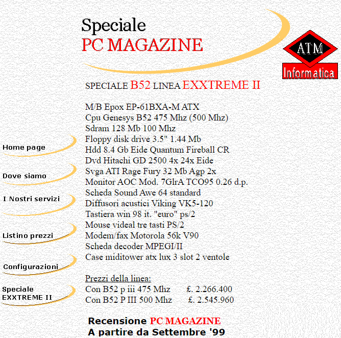
Such a model of a modern PC could have been purchased by the inhabitants of Italy in September 1999. The name of the Genesys B52 475 MHz processor looks interesting. The fastest production Pentium II ran at 450 MHz. But there is an even faster configuration with a frequency of 550 MHz.
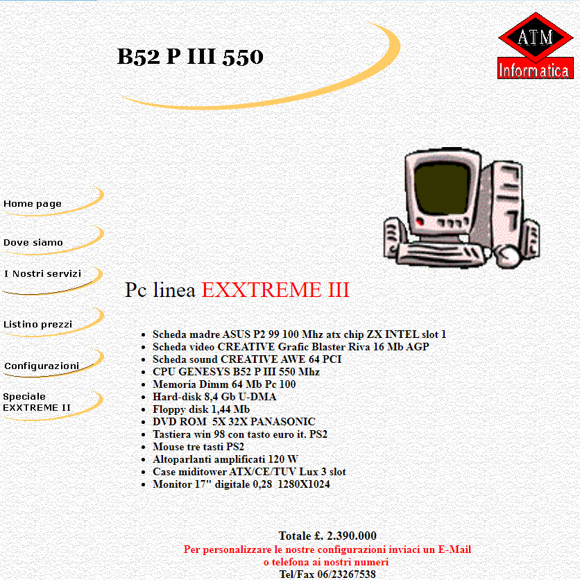
Since the name contains the number III, most likely this processor belongs to the Pentium III Family. And if you look at the price list of that time, then this guess is confirmed.
It should also be noted that the operation of such processors was not guaranteed in all motherboards in a row. If the entire computer was purchased from Genesys, then the BIOS of the motherboard was modified by Genesys specialists. But, if the buyer wanted to buy only a processor, then he received a reminder on this account that he was told what to do before installing the processor in his motherboard. These points looked like this on paper:
1) Save to a file your motherboard BIOS (using the AWDFLASH utility) that you are going to use.
2) Send this file to GENESYS email address.
3) Wait for the corrected file to be returned to your mailbox to use the Genesys B52 CPU and use the AWDFLASH utility to update the motherboard BIOS.
An interesting solution, of course. I will assume that the algorithms (timings) of the L2 cache of the processor were changed in the BIOS. Genesys, of course, took care of the future owners of motherboards in advance and posted a list of motherboards for which modified BIOS versions were available on its website. This is very much the most likely reason that clock for clock, the B52 was still faster.
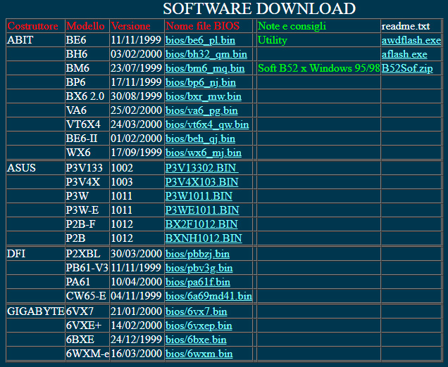
Interestingly, there was also software for Windows95/98, but I could not find these files, even with the Web archive.
Court
Naturally, such a state of affairs, when there was a faster and cheaper analogue of the original Pentium II, even in distant Italy the lawyers at Intel then could not stand for it. If you noticed, the article refers to the processor model as “Genesys B52 MMX”, but the photographs do not show the “MMX” prefix. But, I managed to find a not very good quality photo of those years, where the very first revision of this processor is captured.
And the “reason” of the disappearance of “MMX” is just the handiwork of Intel. As soon as news about the magic processor began to penetrate the media, Intel also learned about such an ‘illegal’, from its point of view, production. Genesys emphasized in every possible way that they only “assemble” their processor, that is, they assemble it from components from other manufacturers. That said, it does not violate any Intel patents, after all, Intel manufactures processor boards and processor cores. This is also not a fake, since Genesys sells the CPU under its own name, and not as an Intel processor. These were the reasons Genesys had then.
In 1998, Intel filed a lawsuit against Genesys, asking a court in Rome to confiscate the processors produced by Genesys and ban them from further production. An initial court decision in February 1999 required the requisition of all processors on the market and a ban on the “B52 MMX” brand, but acknowledged that the manipulation of Intel processors was legal and open in its own right. Therefore, the violation was a ban on the use of the ‘MMX’ trademark, which was owned by Intel. “The damage, however, was not big,” Marcello Console explained at the time. “Until then, we only sold 150 microprocessors.”
As a result, Intel managed to “squeeze” Genesys due to the use of the MMX trademark, but the enterprising Marcello Console quickly changed the logo, removing their text of the MMX model name. This course of events naturally angered Intel even more, and they already wanted to completely destroy the young and enterprising Italian company, which they claimed was preventing it from making its own profit, although reputation was more important in this case.
A second trial followed. This time, Intel insisted that the motherboard modification was tuned to frequencies other than those recommended by Intel, and the result was a more sophisticated product. But for the second time, the Court sided with the Italian company again, finding nothing illegal in such modifications. In June 1999, a third trial took place, in which Intel rejected a new appeal and a subsequent request for damages in the amount of 2.4 billion lire ($1.44 Million USD). In response, Genesys filed a counterclaim for non-pecuniary damage and loss of profits in the amount of $ 18 billion. “But we are open to friendly solutions and technical cooperation with Intel,” Marcello Console assured then.
As everyone understands, such a struggle exhausts a weak opponent, and it is almost useless to fight against Intel, with its resources. As a result, the ending of this story ended not in favor of Genesys. Though they won the battles, they had lost the war, This was likely Intel’s intent all along, as it was their blueprint throughout the 1990’s (See the ‘338 Patent and how Intel abused it). How many “B52” processors were sold is not known, but rather their circulation was insignificant, so such a sample is now very difficult to find and every collector of processors wants to get it.
Conclusion
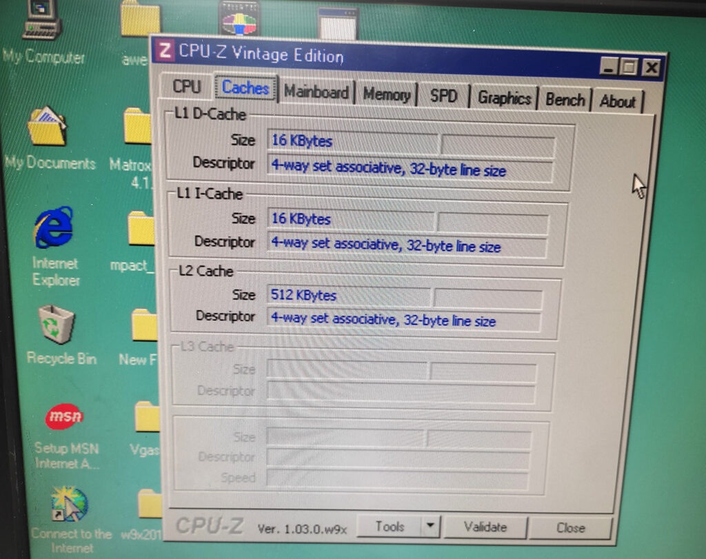
Genesys had no doubt talented engineers and marketers. In fact, the emergence of such processors became possible thanks to overclocking. Many companies at the turn of the 2000s succeeded in selling overclocked processors, but Genesys went the farthest, modifying part of the processor itself – L2 cache and possibly something else. In conclusion, I will provide a couple of screenshots of the CPU-Z Genesys B52 processor:
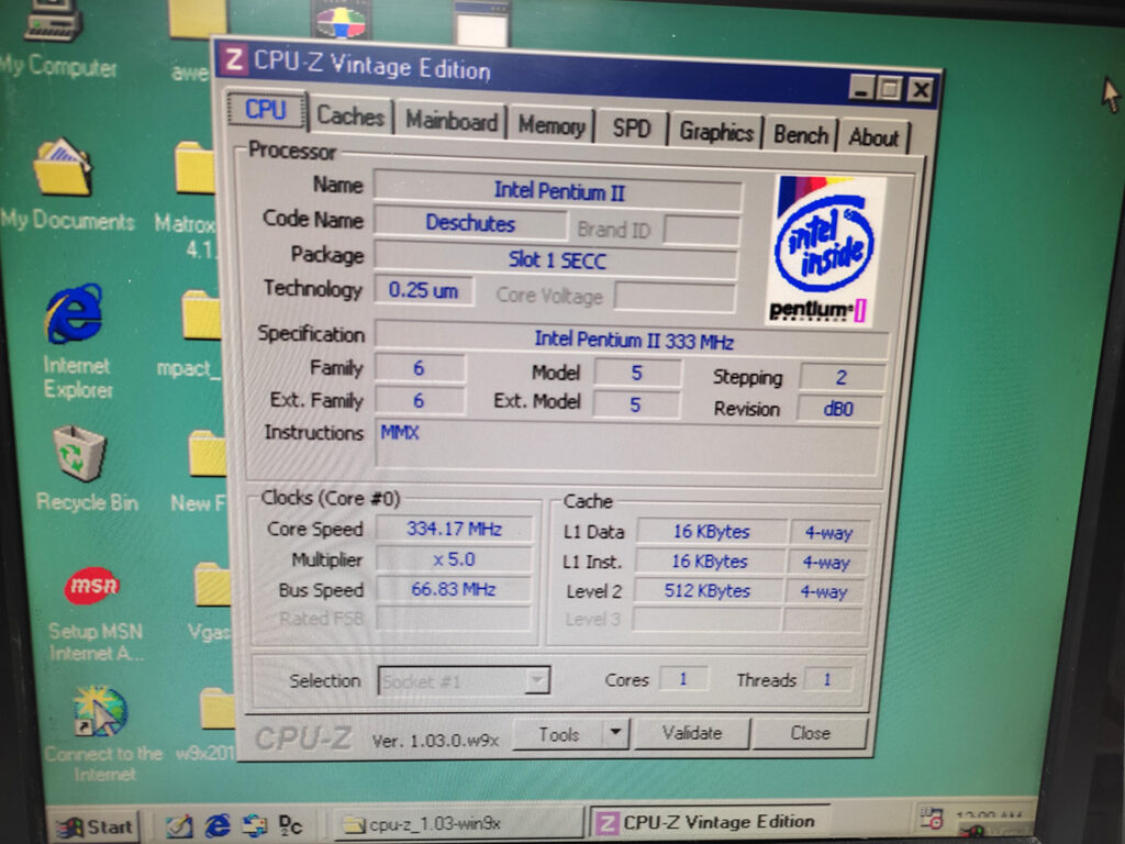
As you can see, this is a Pentium II with a “Deschutes” core with dB0 stepping (Same as the SL2W8 PII 300).
Now it is not easy to find any information about Genesys and its processor, but if you know anything else, write about these facts in the comments to this article. It would be nice to test of of these beasts with something that can capture cache timings/setting (perhaps AIDA?) and maybe get a hint of the BIOS work Genesys did.

Finally, I would like to express my gratitude to Erjon Katrini from Italy for the provided photos of this unique processor! He shared them with me, and I with you, without them this article would not exist.
Author: max1024