A CPU is a terrifically complex piece of hardware. Even Intel’s most lightweight processors comprise more than 40 million transistors on a piece of silicon the size of a fingernail. And it isn’t only about numbers: the way these transistors implement the core logic that drives laptops and desktop PCs is the product of some seriously advanced electronic engineering.
Although the physical construction of CPUs may be abstruse, it isn’t hard to understand the principles of how modern processors are designed, and how they work. An understanding of how instructions are processed inside the CPU can also help programmers construct their code so it will run as quickly and efficiently as possible – although these days much processor optimization is handled automatically by the compiler.
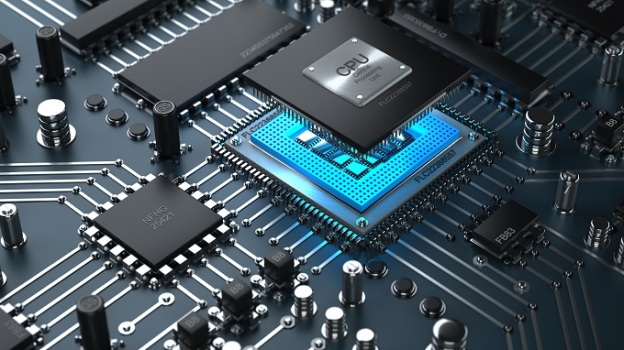
Constructing A CPU
When we picture a CPU, you probably think of a small square of circuit board with a metal casing mounted on it. This is the CPU “package”. The casing isn’t removable, but if you were to pull it off you’d find a small square of silicon below it. This is the die, which contains the functional features of the CPU.
These features take the form of millions of transistors, etched into the silicon by a process called photolithography. Simply put, this involves projecting a design onto a sheet of silicon, using light-sensitive chemicals to “paint” this image onto the surface, then using corrosive agents to etch away the uncoated areas. By stacking multiple photolithographed layers together, it’s possible to make working 3D electronic circuits at a minuscule scale.
The precise scale of these transistors is usually expressed in micrometres (µm) or nanometres (nm), reflecting the size of the smallest feature that can be produced by a given fabrication process. Chip manufacturers are constantly shrinking the process size of their chips: the original Intel 80386 processor was manufactured using a 1.5µm process; the first Pentium IV models used a 180nm process; and the latest Core i7 processors are the product of a 32nm process.
Shrinking the process size enables manufacturers to produce ever more complex chips without commensurately increasing the size of the die. For example, the old Intel 80386 comprised 275,000 transistors; thanks to process shrinkage, a Core i7-7700K processor crams over 1.75 billion transistors.
This is good for several reasons. First, producing high-grade silicon is expensive. A smaller die means lower material costs, so the chips can be sold cheaply and the manufacturer can still make a healthy profit on each one.
Ordinarily, when you shrink a transistor it also requires less power to operate, and burns off less energy as heat. This means smaller transistors can run at higher frequencies without overheating, giving a free performance boost. Since they draw less power, they’re better for the environment – and also, in the case of laptops and mobile devices, for battery life.
Regardless of the process size, all chips generate some heat. This is conducted away by the metal casing, and from there to an external cooler unit. The maximum amount of heat that a chip is expected to dissipate is referred to as its Thermal Design Power (TDP), measured in watts. It doesn’t necessarily indicate how much power a processor will draw in real-world use, but you can expect a chip with a 35W TDP to draw less power than one with a 65W TDP.
The CPU’s neighborhood
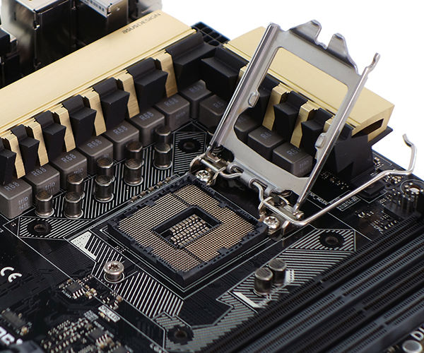
The CPU fits into a dedicated socket on a compatible motherboard, which connects it to the rest of the system components. Until a few years ago, communication between the CPU and other components was mediated by two chips on the motherboard: the “north bridge” dealt with high-speed connections such as PCI Express and memory buses, and the “south bridge” handled lower-bandwidth components such as sound cards and hard disks. Together, these chips were called the chipset.
In modern designs, the memory controllers – and, sometimes, the PCI Express controllers too – are built directly into the processor, which makes things faster and more efficient. Motherboards still offer a range of chipsets, however, supporting different features. For example, the Intel H67 Express chipset supports the integrated graphics processors that are built into current Core i3, i5 and i7 processors. The P67 Express chipset doesn’t support onboard graphics, but does enable overclocking (on CPU models that support it). On the AMD side, the 870 chipset allows the motherboard to offer a single PCI Express x16 slot, while the 890FX chipset can support up to four such slots. Many AMD chipsets also include a low-power GPU, since AMD’s Athlon and Phenom processors don’t have graphics inside the chips themselves.
CPUs Workload
Clearly, the CPU is a highly sophisticated piece of electronic engineering. But in terms of what it actually does, you can think of it as essentially a calculator, whose primary function is to apply simple mathematical operations to the values stored in its internal registers. It can also copy these register contents to and from the computer’s main memory as needed.
Fundamentally, therefore, computer programming is a process of preparing the appropriate instructions to be performed in the right order on the appropriate data. Originally, this was done in assembly language – a system of codes that directly represent the CPU’s internal instructions. These days it’s more usual to write in languages such as C++, and to use compiler software to translate your program into native machine code. The principle is the same, however.
When the CPU executes a program, each instruction goes through a four-stage cycle. First, the instruction code is fetched from memory. Then it’s decoded to determine the actual instruction required. If the instruction requires a piece of data to be fetched from the main memory, this is done. Finally, the instruction is executed, and any output is written to memory, or to an internal register. Execution then continues with the next instruction code.
If you think of the CPU as a clockwork mechanism, each stage of this process represents a “tick” – more formally known as a clock cycle. The number of ticks the CPU completes per second represents its operating frequency, or clock speed. A typical CPU might have a frequency of around 2GHz – equivalent to two billion cycles per second. (In fact, modern processors can automatically adjust their frequencies to suit the workload – see SpeedStep and Turbo Boost – but for the purposes of this example, let’s assume the frequency is constant.) If each instruction goes through a four-stage process, you’d expect a 2GHz CPU core to complete 500 million instructions per second. In fact, modern CPUs can do rather better than this, thanks to an approach called pipelining.
Pipelining – Is CPU a PLUMBER !
In the four-stage cycle described above, each stage of the instruction cycle is carried out by a different part of the core; for example, once the instruction fetcher has retrieved an instruction and handed it over to the decoder unit, it has nothing more to do. Pipelining takes advantage of this by immediately putting the fetcher to work on the next instruction, while the decoder unit is doing its job – and so on along the chain. This means all the parts of the CPU can be working at once, and in theory one instruction can be completed in every single clock cycle.
In practice, the system isn’t quite this efficient. We’ve assumed that each stage in the pipeline takes one clock cycle to complete, but in reality the execution stage can often take several cycles, depending on the complexity of the instruction. On an Intel Sandy Bridge processor, for example, multiplying two 32-bit values together takes four cycles, and dividing one value by another takes 26 cycles. While these operations are being processed, the pipeline can’t progress. Depending on the nature of your code, a core could fall far short of executing one instruction per clock cycle.
Pipelining can also fail when a conditional branch instruction is encountered – that is, where the flow of the program is potentially diverted according to a logical test. Such branches are a basic ingredient of programming: even the most casual tinkerer will recognise constructions such as “IF X<5 THEN GOTO 20”. But such constructions are anathema to pipelining. Until the logical test is processed – at the end of the pipeline – the fetcher has no way of knowing whether it should be continuing to fetch the next instruction in sequence, or whether it should be branching to a different point in the program.
So the fetcher makes an educated guess, with the help of a dedicated circuit called a branch predictor. This component tries to predict what the outcome of the logical test will be, based on the outcome of previous similar operations. On this basis, the fetcher continues speculatively loading instructions into the pipeline. But the branch predictor can’t be right all the time, and when it’s wrong the pipelined instructions must be discarded, leading to wasted cycles as the pipeline is refilled.
What’s more, although we’ve characterised the execution cycle as a four-stage process, modern CPU architectures typically break the work down into many smaller stages. Intel’s Core 2 Duo models, for example, use a 14-stage pipeline, and the Pentium D that preceded them had 31 stages. Depending on the processor, a failed branch prediction could mean discarding a dozen pipelined instructions or more – and wasting that many cycles.
Cache Memory : Out Of Order Executions (OoOE)
There’s a further problem with the pipeline model as we’ve described it above. In our examples, we’ve assumed that fetching instructions and data from the system memory can be done in one clock cycle. In reality, depending on the speed of your DIMMs and CPU, it can easily take 15 cycles or more to load a value from memory into a CPU register.
Obviously, it’s hugely inefficient for the CPU to sit idle for 15 cycles every time it needs to access a value from memory. To work around this, modern processors use two approaches. The first is caching: building small amounts of very fast memory directly onto the CPU, and using this whenever possible, rather than accessing the slower system RAM. A different part of the CPU takes care of synchronising this cached data with main memory, while the execution unit gets on with other tasks.
Modern processors use a multilevel cache system: the smallest and fastest cache is level one (L1), which is used for storing instructions and data, and typically has a capacity of 64KB or 128KB. Then come larger, slower L2 and L3 caches, with sizes measured in megabytes. This very fast, on-chip RAM is expensive to produce, so a common way to reduce the costs is by shrinking or removing caches – but this has a detrimental effect on performance.
In addition to caching, processors can also implement out-of-order execution (OoOE). This means what it says: in an OoOE pipeline, instructions don’t have to be processed in strict sequence, but can overtake one another. If one instruction is held up waiting for data to arrive from the main memory, the CPU can continue to process other instructions that were behind it in the pipeline, and come back to the instruction when it’s ready to be executed.
Clearly, there are limits to OoOE. The CPU can’t just skim back and forth between instructions as it sees fit, or programs wouldn’t work as intended. A buffering system is used to ensure instructions take effect in the right order, even if they were executed out of sequence.
However, OoOE can still save a lot of time – for example, by allowing the execution unit to get started on a slow calculation while another instruction is waiting for its data to arrive from main memory. That sort of optimisation can make a big difference, so almost all modern processors use OoOE. The notable exception is Intel’s Atom range – which is one reason why Atom-powered devices feel sluggish compared to mainstream processors.
Threading and Cores
So far we’ve focused on the workings of an individual CPU core; but most current processors combine two or four cores. This allows them to chew through multiple instructions at once, which in turn means you can run more programs smoothly at once. Of course, you can multitask on a single core CPU; but this is achieved by “time-slicing”, rather than true simultaneous processing, and it’s apt to deliver uneven performance.
Having a multicore processor won’t ordinarily make individual programs run any faster. This is because most programs are designed to run in a strict linear fashion – so the second instruction, for example, must be executed after the first has completed, not at the same time. This sequential process – this “thread”, as it’s called – has no way to make use of additional CPU cores.
Some types of task, however, can be divided into multiple threads. For example, imagine a program that’s designed to convert a folder full of audio files into MP3 format. On detecting that it was running on a quad-core processor, such a program might spawn four independent encoding processes, and hand one to each CPU core. In this way, the total encoding time could be quartered. Applications for 3D rendering can typically divide up their workload in a similar way.
Intel processors use a feature called Hyper-Threading to gain additional throughput. Each core in a Hyper-Threading CPU appears to the operating system as two virtual cores. In reality, the core can only process a single instruction at once – but it has two sets of registers, enabling it to switch its attention back and forth between two threads to make the most efficient use of its processing capacity. Predictably, the benefit is less than you’d see from two physical cores. But in our benchmarks we’ve seen Hyper-Threading prove its worth, giving multithreaded tasks a performance boost of around 30%.
The Extended Instructions
Earlier we characterised the CPU as “essentially a calculator”; this isn’t a bad analogy, but the modern CPU boasts several sophistications that your average Casio can only dream of.
For one thing, the conventional pocket calculator can handle up to eight digits only, so the largest number that can be represented is 99,999,999. All modern CPUs can operate on 32-bit binary data, enabling them to work directly with values up to 4,294,967,296. Most also support 64-bit operation (when used with a 64-bit operating system), for values up to 18,446,744,073,709,551,656. This means they can work with huge numbers at full speed with perfect accuracy. It also means a 64-bit operating system can support millions of terabytes of memory, while 32-bit systems are limited to 4GB (of which, in practice, only around 3.5GB is usable in Windows).
In addition to regular calculator operations, CPUs also support “extensions” that accelerate certain types of task. The SSE extensions found in every modern processor are a good example: the acronym stands for Streaming SIMD Extensions, with SIMD in turn standing for Single Instruction, Multiple Data. In practice, one SSE instruction can make the processor tear through a data set applying a single operation – such as addition or subtraction – to every data element in the set in a fraction of the time it would take to process each element individually. Implementing these special instructions involves considerable engineering work at the design stage, but once the feature is there it can give an enormous boost to tasks such as video processing and data compression.
Another sort of extension that’s commonly found in modern processors is hardware virtualisation. Conventionally, virtualisation software acts as a middle man between the virtual environment and the real hardware resources, which can slow things down considerably. Virtualisation extensions allow code running in the virtual machine to execute directly on the processor, at full speed – but instructions that can’t be executed natively are automatically trapped, so they can be handled by the virtualisation host software.
Extensions can also be used to provide security. Intel’s 2010 range of Core i3, i5 and i7 processors brought a new set of extensions called AES-NI, which enable the processor to encrypt and decrypt data using the industry-standard AES encryption algorithm at accelerated speeds. Intel’s TXT (Trusted Execution Technology) prevents programs from carrying out potentially dangerous activities, such as modifying resources that are being used by another process or snooping on the keyboard and mouse. An extension called Data Execution Prevention prevents the processor from running code that wasn’t loaded into memory as such: this makes it harder for viruses and hacker attacks to sneak onto the system.
With all these extensions and features, the modern CPU is far more than a simple calculator. In fact, it’s a miracle of engineering. When you reflect that the microprocessor was invented only a short half-century ago, it’s incredible to think what’s been accomplished… and there’s no sign of that progress slowing down any time soon.
Steppings : The horrible naming
There are many different types of processor on the market. Some are designed for servers and workstations; some are designed for netbooks and low-power laptops.
But within a given family, it’s likely that most models will use the same core design. For example, consider AMD’s Athlon II X4 640, Phenom II X4 940 and Phenom II X4 980 processors. They perform quite differently, but that’s thanks to differing amounts of L3 cache and differing clock speeds. The physical arrangement of transistors inside the different models is functionally identical.
This approach makes commercial sense because setting up a photolithographic process isn’t cheap. But it means that if any bugs sneak into the process, they’ll affect the entire processor family. AMD knows this to its cost: when it launched the first Phenom processors back in 2007, every model suffered from a serious bug that reduced performance by at least 10%.
In such cases, the only thing to do is to revise the design and introduce what’s called a new “stepping”. In this instance, the faulty chips were made from a design that had the stepping code B2; some months later, when AMD started to produce chips from an updated design, this was known as the B3 stepping. (The first testing design of a processor is commonly given the stepping A0, with subsequent major changes represented by a new letter and minor changes by incrementing the number.)
Even when there isn’t a problem with a chip, it’s common for processors to go through a few steppings over their lifetimes. Intel’s first range of Core i7 processors, released in 2008, had the stepping code C0; but if you’d bought one of the same models a year later, it would have been a D0 stepping. No major changes were announced, but overclockers found D0 models more stable at very high speeds. Presumably Intel found a way to simplify the design, making it more stable and increasing the proportion of chips that come out of the manufacturing process in perfect working order – the “yield”, in industry jargon.
Turbo Boost and SpeedStep : The Race begins here
We traditionally think of a processor as running at a set frequency, but for more than a decade almost all CPUs have had the ability to dynamically adjust their clock speeds. Intel’s SpeedStep technology, first introduced with the Pentium III processor, detects when the processor isn’t being used to its full capacity and automatically turns the speed down. When the processor is taxed, the speed immediately ramps up again. This lets the computer deliver full performance when the user wants it, while generating less heat and consuming less power when the user is doing something passive, such as reading a web page. AMD processors have had the same ability for just as long, under the name PowerNow! for mobile chips and Cool’n’Quiet for desktop processors.
With the introduction of the Core i7 in 2008, Intel extended the principle to run in the other direction as well, with a new feature called Turbo Boost. It took advantage of the fact that quad-core i7 chips were designed with a TDP to accommodate all four cores being used simultaneously. When only one or two cores were in use, it was possible to automatically increase the speed of those cores while remaining within the overall heat and power budget.
In modern Core i5 and i7 processors, Turbo Boost is more aggressive, and can kick in even when all four cores are active. And AMD has followed suit, with the similarly-named Turbo Core system appearing in the six-core Phenom II X6 range, and more recently on some models of its A-Series processors. So when you next buy, say, a 2GHz processor, it’s likely it will in fact spend most of its time running well below that speed – and a fair proportion running well above it.
Sources : wiki, pc authority, self, google.

Well explained in a very concise manner.
LikeLiked by 1 person
Thank you ! Anything else you would like me to explain ?
LikeLike