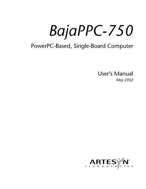
BajaPPC-750 User's Manual - Emerson Network Power
BajaPPC-750 User's Manual - Emerson Network Power
BajaPPC-750 User's Manual - Emerson Network Power

You also want an ePaper? Increase the reach of your titles
YUMPU automatically turns print PDFs into web optimized ePapers that Google loves.
<strong>BajaPPC</strong>-<strong>750</strong><br />
<strong>Power</strong>PC-Based, Single-Board Computer<br />
User’s <strong>Manual</strong><br />
May 2002
Artesyn Communication Products<br />
8310 Excelsior Dr.<br />
Madison, WI 53717<br />
Web Site: www.artesyncp.com<br />
Sales: (800) 356-9602<br />
Technical Support: (800) 327-1251<br />
<strong>BajaPPC</strong>-<strong>750</strong> User’s <strong>Manual</strong>—Artesyn Part Number: 0002M621-15
<strong>BajaPPC</strong>-<strong>750</strong><br />
<strong>Power</strong>PC-Based, Single-Board Computer<br />
User’s <strong>Manual</strong><br />
May 2002
The information in this manual has been checked and is believed to be accurate<br />
and reliable. HOWEVER, NO RESPONSIBILITY IS ASSUMED BY ARTESYN COM-<br />
MUNICATION PRODUCTS FOR ITS USE OR FOR ANY INACCURACIES. Specifications<br />
are subject to change without notice. ARTESYN COMMUNICATION<br />
PRODUCTS DOES NOT ASSUME ANY LIABILITY ARISING OUT OF USE OR<br />
OTHER APPLICATION OF ANY PRODUCT, CIRCUIT, OR PROGRAM DESCRIBED<br />
HEREIN. This document does not convey any license under Artesyn Communication<br />
Products patents or the rights of others.<br />
Artesyn and the Artesyn logo are registered trademarks of Artesyn Technologies<br />
and are used by Artesyn Communication Products under licence from Artesyn<br />
Technologies. All other trademarks are property of their respective owners.<br />
Revision History<br />
Revision Level Principal Changes Publication Date Board Rev.<br />
0002M621-A First publication July 1999 1<br />
0002M621-10 Update jumper settings October 1999 1<br />
0002M621-11 Updated PCB artwork February 2000 21<br />
0002M621-12 Update Fig. 2-5 and Section 4.4 July 2000 21<br />
0002M621-13 Remove reference to software reset bit November 2000 21<br />
0002M621-14 Update for board revision August 2001 22<br />
0002M621-15 New board rev. & update Table 10-3 May 2002 23<br />
Copyright © 1999–2002 Artesyn Communication Products All rights reserved.
Regulatory Agency Warnings & Notices<br />
The Artesyn <strong>BajaPPC</strong>-<strong>750</strong> is certified by the Federal Communications Commission (FCC)<br />
according to Title 47 of the Code of Federal Regulations, Part 15. The following information<br />
is provided as required by this agency.<br />
FCC Rules and Regulations – Part 15<br />
This equipment has been tested and found to comply with the limits for a Class B digital<br />
device, pursuant to part 15 of the FCC Rules. These limits are designed to provide reasonable<br />
protection against harmful interference in a residential installation. This equipment<br />
generates, uses and can radiate radio frequency energy and, if not installed and used in<br />
accordance with the instructions, may cause harmful interference to radio communications.<br />
However, there is no guarantee that interference will not occur in a particular installation.<br />
If this equipment does cause harmful interference to radio or television reception,<br />
which can be determined by turning the equipment off and on, the user is encouraged to<br />
try to correct the interference by one or more of the following measures:<br />
Reorient or relocate the receiving antenna<br />
Increase the separation between the equipment and receiver<br />
Connect the equipment into an outlet on a circuit different from that to which the<br />
receiver is connected<br />
Consult the dealer or an experienced radio/TV technician for help<br />
CAUTION. Making changes or modifications to the <strong>BajaPPC</strong>-<strong>750</strong> without the<br />
explicit consent of Artesyn Communication Products could invalidate<br />
the user’s authority to operate this equipment.
1. Overview<br />
2. Setup<br />
Contents<br />
1.1 Components and Features . . . . . . . . . . . . . . . . . . . . . . . . . . . . . . . . . . . . . . . . . . . . . . . . . . . .1-1<br />
1.2 Functional Description . . . . . . . . . . . . . . . . . . . . . . . . . . . . . . . . . . . . . . . . . . . . . . . . . . . . . . .1-3<br />
1.3 Physical Memory Map . . . . . . . . . . . . . . . . . . . . . . . . . . . . . . . . . . . . . . . . . . . . . . . . . . . . . . .1-4<br />
1.4 Additional Information . . . . . . . . . . . . . . . . . . . . . . . . . . . . . . . . . . . . . . . . . . . . . . . . . . . . . . .1-6<br />
1.4.1 Product Certifications . . . . . . . . . . . . . . . . . . . . . . . . . . . . . . . . . . . . . . . . . . . . . . . .1-6<br />
1.4.2 Terminology and Notation . . . . . . . . . . . . . . . . . . . . . . . . . . . . . . . . . . . . . . . . . . . .1-7<br />
1.4.3 Technical References . . . . . . . . . . . . . . . . . . . . . . . . . . . . . . . . . . . . . . . . . . . . . . . . .1-7<br />
2.1 Electrostatic Discharge . . . . . . . . . . . . . . . . . . . . . . . . . . . . . . . . . . . . . . . . . . . . . . . . . . . . . . .2-1<br />
2.2 <strong>BajaPPC</strong>-<strong>750</strong> Circuit Board . . . . . . . . . . . . . . . . . . . . . . . . . . . . . . . . . . . . . . . . . . . . . . . . . . . .2-2<br />
2.2.1 Component Maps and Jumpers . . . . . . . . . . . . . . . . . . . . . . . . . . . . . . . . . . . . . . . . .2-2<br />
2.2.2 Serial Numbers . . . . . . . . . . . . . . . . . . . . . . . . . . . . . . . . . . . . . . . . . . . . . . . . . . . .2-12<br />
2.2.3 Connectors . . . . . . . . . . . . . . . . . . . . . . . . . . . . . . . . . . . . . . . . . . . . . . . . . . . . . . .2-12<br />
2.2.4 Reset/Interrupt Switch . . . . . . . . . . . . . . . . . . . . . . . . . . . . . . . . . . . . . . . . . . . . . . .2-13<br />
2.2.5 LED . . . . . . . . . . . . . . . . . . . . . . . . . . . . . . . . . . . . . . . . . . . . . . . . . . . . . . . . . . . . .2-13<br />
2.2.6 Optional VMEbus Configurations. . . . . . . . . . . . . . . . . . . . . . . . . . . . . . . . . . . . . . .2-14<br />
2.3 <strong>BajaPPC</strong>-<strong>750</strong> Setup . . . . . . . . . . . . . . . . . . . . . . . . . . . . . . . . . . . . . . . . . . . . . . . . . . . . . . . . .2-14<br />
2.3.1 Providing <strong>Power</strong> . . . . . . . . . . . . . . . . . . . . . . . . . . . . . . . . . . . . . . . . . . . . . . . . . . .2-15<br />
2.3.2 Providing Air Flow . . . . . . . . . . . . . . . . . . . . . . . . . . . . . . . . . . . . . . . . . . . . . . . . . .2-15<br />
2.4 Operational Checks . . . . . . . . . . . . . . . . . . . . . . . . . . . . . . . . . . . . . . . . . . . . . . . . . . . . . . . .2-16<br />
2.5 Reset Methods . . . . . . . . . . . . . . . . . . . . . . . . . . . . . . . . . . . . . . . . . . . . . . . . . . . . . . . . . . . .2-16<br />
2.6 Troubleshooting . . . . . . . . . . . . . . . . . . . . . . . . . . . . . . . . . . . . . . . . . . . . . . . . . . . . . . . . . . .2-17<br />
2.6.1 Technical Support . . . . . . . . . . . . . . . . . . . . . . . . . . . . . . . . . . . . . . . . . . . . . . . . . .2-18<br />
2.6.2 Service Information . . . . . . . . . . . . . . . . . . . . . . . . . . . . . . . . . . . . . . . . . . . . . . . . .2-18<br />
3. Central Processing Unit<br />
3.1 Processor Reset . . . . . . . . . . . . . . . . . . . . . . . . . . . . . . . . . . . . . . . . . . . . . . . . . . . . . . . . . . . . .3-2<br />
3.2 Processor Initialization. . . . . . . . . . . . . . . . . . . . . . . . . . . . . . . . . . . . . . . . . . . . . . . . . . . . . . . .3-2<br />
3.2.1 Hardware Implementation Dependent Register . . . . . . . . . . . . . . . . . . . . . . . . . . . . .3-3<br />
3.2.2 Machine State Register . . . . . . . . . . . . . . . . . . . . . . . . . . . . . . . . . . . . . . . . . . . . . . .3-4<br />
3.3 Exception Handling . . . . . . . . . . . . . . . . . . . . . . . . . . . . . . . . . . . . . . . . . . . . . . . . . . . . . . . . .3-6<br />
3.4 Interrupt Handling . . . . . . . . . . . . . . . . . . . . . . . . . . . . . . . . . . . . . . . . . . . . . . . . . . . . . . . . . .3-7<br />
0002M621-15 i
3.5 Bus Speed . . . . . . . . . . . . . . . . . . . . . . . . . . . . . . . . . . . . . . . . . . . . . . . . . . . . . . . . . . . . . . . . .3-8<br />
3.6 Cache Memory . . . . . . . . . . . . . . . . . . . . . . . . . . . . . . . . . . . . . . . . . . . . . . . . . . . . . . . . . . . . .3-8<br />
3.6.1 Integrated Level 2 Cache . . . . . . . . . . . . . . . . . . . . . . . . . . . . . . . . . . . . . . . . . . . . . .3-9<br />
3.7 JTAG/COP Interface. . . . . . . . . . . . . . . . . . . . . . . . . . . . . . . . . . . . . . . . . . . . . . . . . . . . . . . . .3-10<br />
3.8 Debug Header . . . . . . . . . . . . . . . . . . . . . . . . . . . . . . . . . . . . . . . . . . . . . . . . . . . . . . . . . . . .3-11<br />
4. On-Card Memory Configuration<br />
4.1 MPC106 Memory Interface . . . . . . . . . . . . . . . . . . . . . . . . . . . . . . . . . . . . . . . . . . . . . . . . . . . .4-1<br />
4.2 Boot Memory Configuration . . . . . . . . . . . . . . . . . . . . . . . . . . . . . . . . . . . . . . . . . . . . . . . . . . .4-2<br />
4.3 User Flash . . . . . . . . . . . . . . . . . . . . . . . . . . . . . . . . . . . . . . . . . . . . . . . . . . . . . . . . . . . . . . . . .4-3<br />
4.4 On-Card SDRAM. . . . . . . . . . . . . . . . . . . . . . . . . . . . . . . . . . . . . . . . . . . . . . . . . . . . . . . . . . . .4-3<br />
4.4.1 SDRAM Configuration . . . . . . . . . . . . . . . . . . . . . . . . . . . . . . . . . . . . . . . . . . . . . . . .4-4<br />
4.4.2 SDRAM Timing . . . . . . . . . . . . . . . . . . . . . . . . . . . . . . . . . . . . . . . . . . . . . . . . . . . . .4-4<br />
4.5 Real-Time Clock . . . . . . . . . . . . . . . . . . . . . . . . . . . . . . . . . . . . . . . . . . . . . . . . . . . . . . . . . . . .4-6<br />
4.6 Nonvolatile Memory Map . . . . . . . . . . . . . . . . . . . . . . . . . . . . . . . . . . . . . . . . . . . . . . . . . . . . .4-8<br />
5. PMC/PCI Interface<br />
5.1 Features . . . . . . . . . . . . . . . . . . . . . . . . . . . . . . . . . . . . . . . . . . . . . . . . . . . . . . . . . . . . . . . . . .5-1<br />
5.2 PMC Module Installation. . . . . . . . . . . . . . . . . . . . . . . . . . . . . . . . . . . . . . . . . . . . . . . . . . . . . .5-2<br />
5.3 PCI Bridge Configuration Registers . . . . . . . . . . . . . . . . . . . . . . . . . . . . . . . . . . . . . . . . . . . . . .5-3<br />
5.3.1 PCI Command Register . . . . . . . . . . . . . . . . . . . . . . . . . . . . . . . . . . . . . . . . . . . . . . .5-4<br />
5.3.2 PCI Status Register . . . . . . . . . . . . . . . . . . . . . . . . . . . . . . . . . . . . . . . . . . . . . . . . . . .5-5<br />
5.4 PCI Interface . . . . . . . . . . . . . . . . . . . . . . . . . . . . . . . . . . . . . . . . . . . . . . . . . . . . . . . . . . . . . . .5-6<br />
5.4.1 Device Mapping . . . . . . . . . . . . . . . . . . . . . . . . . . . . . . . . . . . . . . . . . . . . . . . . . . . .5-6<br />
5.4.2 Timing . . . . . . . . . . . . . . . . . . . . . . . . . . . . . . . . . . . . . . . . . . . . . . . . . . . . . . . . . . . .5-7<br />
5.4.3 Interrupts. . . . . . . . . . . . . . . . . . . . . . . . . . . . . . . . . . . . . . . . . . . . . . . . . . . . . . . . . .5-7<br />
5.4.4 Arbitration . . . . . . . . . . . . . . . . . . . . . . . . . . . . . . . . . . . . . . . . . . . . . . . . . . . . . . . . .5-7<br />
5.5 PCI Bus Control Signals . . . . . . . . . . . . . . . . . . . . . . . . . . . . . . . . . . . . . . . . . . . . . . . . . . . . . . .5-8<br />
5.6 PMC Connector Pin Assignments . . . . . . . . . . . . . . . . . . . . . . . . . . . . . . . . . . . . . . . . . . . . . .5-10<br />
6. VMEbus Interface<br />
6.1 Features . . . . . . . . . . . . . . . . . . . . . . . . . . . . . . . . . . . . . . . . . . . . . . . . . . . . . . . . . . . . . . . . . .6-1<br />
6.2 Universe Configuration Registers. . . . . . . . . . . . . . . . . . . . . . . . . . . . . . . . . . . . . . . . . . . . . . . .6-2<br />
6.2.1 Initialization Values . . . . . . . . . . . . . . . . . . . . . . . . . . . . . . . . . . . . . . . . . . . . . . . . . .6-7<br />
6.2.2 PCI Base Address Register. . . . . . . . . . . . . . . . . . . . . . . . . . . . . . . . . . . . . . . . . . . . . .6-8<br />
6.2.3 PCI Configuration Space and Status Register . . . . . . . . . . . . . . . . . . . . . . . . . . . . . . .6-8<br />
6.2.4 Master Control Register . . . . . . . . . . . . . . . . . . . . . . . . . . . . . . . . . . . . . . . . . . . . . .6-10<br />
6.2.5 Miscellaneous Control Register. . . . . . . . . . . . . . . . . . . . . . . . . . . . . . . . . . . . . . . . .6-11<br />
6.2.6 VMEbus Master Image Registers. . . . . . . . . . . . . . . . . . . . . . . . . . . . . . . . . . . . . . . .6-12<br />
6.2.7 VMEbus Slave Image Registers . . . . . . . . . . . . . . . . . . . . . . . . . . . . . . . . . . . . . . . . .6-13<br />
6.3 VMEbus Master Interface. . . . . . . . . . . . . . . . . . . . . . . . . . . . . . . . . . . . . . . . . . . . . . . . . . . . .6-15<br />
6.3.1 Addressing. . . . . . . . . . . . . . . . . . . . . . . . . . . . . . . . . . . . . . . . . . . . . . . . . . . . . . . .6-16<br />
6.3.2 Data Transfers . . . . . . . . . . . . . . . . . . . . . . . . . . . . . . . . . . . . . . . . . . . . . . . . . . . . .6-17<br />
ii <strong>BajaPPC</strong>-<strong>750</strong>: Contents
6.4 VMEbus Slave Interface. . . . . . . . . . . . . . . . . . . . . . . . . . . . . . . . . . . . . . . . . . . . . . . . . . . . . .6-17<br />
6.4.1 Slave Mapping Example. . . . . . . . . . . . . . . . . . . . . . . . . . . . . . . . . . . . . . . . . . . . . .6-18<br />
6.5 VMEbus Interrupts . . . . . . . . . . . . . . . . . . . . . . . . . . . . . . . . . . . . . . . . . . . . . . . . . . . . . . . . .6-20<br />
6.5.1 Interrupter. . . . . . . . . . . . . . . . . . . . . . . . . . . . . . . . . . . . . . . . . . . . . . . . . . . . . . . .6-21<br />
6.5.2 Interrupt Handler. . . . . . . . . . . . . . . . . . . . . . . . . . . . . . . . . . . . . . . . . . . . . . . . . . .6-21<br />
6.6 VMEbus System Controller . . . . . . . . . . . . . . . . . . . . . . . . . . . . . . . . . . . . . . . . . . . . . . . . . . .6-22<br />
6.7 SYSFAIL Control . . . . . . . . . . . . . . . . . . . . . . . . . . . . . . . . . . . . . . . . . . . . . . . . . . . . . . . . . . .6-22<br />
6.8 Bus Timer . . . . . . . . . . . . . . . . . . . . . . . . . . . . . . . . . . . . . . . . . . . . . . . . . . . . . . . . . . . . . . . .6-22<br />
6.9 Mailboxes . . . . . . . . . . . . . . . . . . . . . . . . . . . . . . . . . . . . . . . . . . . . . . . . . . . . . . . . . . . . . . . .6-22<br />
6.10 Location Monitor . . . . . . . . . . . . . . . . . . . . . . . . . . . . . . . . . . . . . . . . . . . . . . . . . . . . . . . . . .6-24<br />
6.11 Semaphores . . . . . . . . . . . . . . . . . . . . . . . . . . . . . . . . . . . . . . . . . . . . . . . . . . . . . . . . . . . . . .6-25<br />
6.12 VMEbus Control Signals . . . . . . . . . . . . . . . . . . . . . . . . . . . . . . . . . . . . . . . . . . . . . . . . . . . . .6-25<br />
6.13 VMEbus Connector Pin Assignments. . . . . . . . . . . . . . . . . . . . . . . . . . . . . . . . . . . . . . . . . . . .6-28<br />
7. Ethernet Interface<br />
7.1 21143 Registers . . . . . . . . . . . . . . . . . . . . . . . . . . . . . . . . . . . . . . . . . . . . . . . . . . . . . . . . . . . .7-1<br />
7.1.1 Configuration . . . . . . . . . . . . . . . . . . . . . . . . . . . . . . . . . . . . . . . . . . . . . . . . . . . . . .7-2<br />
7.1.2 Command/Status . . . . . . . . . . . . . . . . . . . . . . . . . . . . . . . . . . . . . . . . . . . . . . . . . . .7-2<br />
7.2 Ethernet Address. . . . . . . . . . . . . . . . . . . . . . . . . . . . . . . . . . . . . . . . . . . . . . . . . . . . . . . . . . . .7-3<br />
7.3 Default Ethernet Boot Device . . . . . . . . . . . . . . . . . . . . . . . . . . . . . . . . . . . . . . . . . . . . . . . . . .7-4<br />
7.4 21143 Errata. . . . . . . . . . . . . . . . . . . . . . . . . . . . . . . . . . . . . . . . . . . . . . . . . . . . . . . . . . . . . . .7-4<br />
7.5 Ethernet Ports . . . . . . . . . . . . . . . . . . . . . . . . . . . . . . . . . . . . . . . . . . . . . . . . . . . . . . . . . . . . . .7-5<br />
7.5.1 Fast Ethernet . . . . . . . . . . . . . . . . . . . . . . . . . . . . . . . . . . . . . . . . . . . . . . . . . . . . . . .7-5<br />
7.5.2 AUI Ethernet . . . . . . . . . . . . . . . . . . . . . . . . . . . . . . . . . . . . . . . . . . . . . . . . . . . . . . .7-5<br />
7.6 Cabling Considerations. . . . . . . . . . . . . . . . . . . . . . . . . . . . . . . . . . . . . . . . . . . . . . . . . . . . . . .7-6<br />
8. Serial and Parallel I/O<br />
8.1 PCI to ISA Bridge . . . . . . . . . . . . . . . . . . . . . . . . . . . . . . . . . . . . . . . . . . . . . . . . . . . . . . . . . . .8-1<br />
8.1.1 Basic Operation . . . . . . . . . . . . . . . . . . . . . . . . . . . . . . . . . . . . . . . . . . . . . . . . . . . . .8-2<br />
8.1.2 Registers . . . . . . . . . . . . . . . . . . . . . . . . . . . . . . . . . . . . . . . . . . . . . . . . . . . . . . . . . .8-2<br />
8.2 I/O Controller . . . . . . . . . . . . . . . . . . . . . . . . . . . . . . . . . . . . . . . . . . . . . . . . . . . . . . . . . . . . . .8-4<br />
8.2.1 Block Addressing . . . . . . . . . . . . . . . . . . . . . . . . . . . . . . . . . . . . . . . . . . . . . . . . . . . .8-5<br />
8.2.2 Configuration . . . . . . . . . . . . . . . . . . . . . . . . . . . . . . . . . . . . . . . . . . . . . . . . . . . . . .8-5<br />
8.3 Serial Ports . . . . . . . . . . . . . . . . . . . . . . . . . . . . . . . . . . . . . . . . . . . . . . . . . . . . . . . . . . . . . . . .8-8<br />
8.3.1 Serial Port Addressing . . . . . . . . . . . . . . . . . . . . . . . . . . . . . . . . . . . . . . . . . . . . . . . .8-8<br />
8.3.2 Serial Port Registers . . . . . . . . . . . . . . . . . . . . . . . . . . . . . . . . . . . . . . . . . . . . . . . . . .8-8<br />
8.3.3 Programmable Baud Rate . . . . . . . . . . . . . . . . . . . . . . . . . . . . . . . . . . . . . . . . . . . .8-12<br />
8.3.4 Connectors and Cabling . . . . . . . . . . . . . . . . . . . . . . . . . . . . . . . . . . . . . . . . . . . . .8-13<br />
8.3.5 Handshaking Jumper . . . . . . . . . . . . . . . . . . . . . . . . . . . . . . . . . . . . . . . . . . . . . . . .8-15<br />
8.4 Parallel Port (Optional) . . . . . . . . . . . . . . . . . . . . . . . . . . . . . . . . . . . . . . . . . . . . . . . . . . . . . .8-15<br />
8.4.1 Parallel Port Addressing . . . . . . . . . . . . . . . . . . . . . . . . . . . . . . . . . . . . . . . . . . . . . .8-16<br />
8.4.2 Parallel Port Registers. . . . . . . . . . . . . . . . . . . . . . . . . . . . . . . . . . . . . . . . . . . . . . . .8-16<br />
0002M621-15 iii
9. Counter/Timers<br />
9.1 Counter/Timers. . . . . . . . . . . . . . . . . . . . . . . . . . . . . . . . . . . . . . . . . . . . . . . . . . . . . . . . . . . . .9-1<br />
9.2 Counter/Timer Registers . . . . . . . . . . . . . . . . . . . . . . . . . . . . . . . . . . . . . . . . . . . . . . . . . . . . . .9-1<br />
9.2.1 Period Register. . . . . . . . . . . . . . . . . . . . . . . . . . . . . . . . . . . . . . . . . . . . . . . . . . . . . .9-2<br />
9.2.2 Count Register . . . . . . . . . . . . . . . . . . . . . . . . . . . . . . . . . . . . . . . . . . . . . . . . . . . . . .9-2<br />
9.2.3 Status Register . . . . . . . . . . . . . . . . . . . . . . . . . . . . . . . . . . . . . . . . . . . . . . . . . . . . . .9-2<br />
9.2.4 Interrupt Acknowledge Register . . . . . . . . . . . . . . . . . . . . . . . . . . . . . . . . . . . . . . . . .9-3<br />
9.2.5 Mode Register . . . . . . . . . . . . . . . . . . . . . . . . . . . . . . . . . . . . . . . . . . . . . . . . . . . . . .9-4<br />
10. Monitor<br />
10.1 Monitor Features. . . . . . . . . . . . . . . . . . . . . . . . . . . . . . . . . . . . . . . . . . . . . . . . . . . . . . . . . . .10-1<br />
10.1.1 Start-Up Display. . . . . . . . . . . . . . . . . . . . . . . . . . . . . . . . . . . . . . . . . . . . . . . . . . . .10-1<br />
10.1.2 Command-Line History . . . . . . . . . . . . . . . . . . . . . . . . . . . . . . . . . . . . . . . . . . . . . .10-3<br />
10.1.3 Command-Line Editor . . . . . . . . . . . . . . . . . . . . . . . . . . . . . . . . . . . . . . . . . . . . . . .10-3<br />
10.1.4 <strong>Power</strong>PC Debugger . . . . . . . . . . . . . . . . . . . . . . . . . . . . . . . . . . . . . . . . . . . . . . . . .10-4<br />
10.2 Basic Operation. . . . . . . . . . . . . . . . . . . . . . . . . . . . . . . . . . . . . . . . . . . . . . . . . . . . . . . . . . . .10-5<br />
10.2.1 <strong>Power</strong>-Up/Reset Sequence . . . . . . . . . . . . . . . . . . . . . . . . . . . . . . . . . . . . . . . . . . . .10-5<br />
10.2.2 Initializing Memory . . . . . . . . . . . . . . . . . . . . . . . . . . . . . . . . . . . . . . . . . . . . . . . .10-13<br />
10.3 Monitor Command Reference. . . . . . . . . . . . . . . . . . . . . . . . . . . . . . . . . . . . . . . . . . . . . . . .10-13<br />
10.3.1 Command Syntax . . . . . . . . . . . . . . . . . . . . . . . . . . . . . . . . . . . . . . . . . . . . . . . . .10-13<br />
10.3.2 Typographic Conventions . . . . . . . . . . . . . . . . . . . . . . . . . . . . . . . . . . . . . . . . . . .10-14<br />
10.4 Boot Commands. . . . . . . . . . . . . . . . . . . . . . . . . . . . . . . . . . . . . . . . . . . . . . . . . . . . . . . . . .10-14<br />
10.4.1 bootbus . . . . . . . . . . . . . . . . . . . . . . . . . . . . . . . . . . . . . . . . . . . . . . . . . . . . . . . . .10-14<br />
10.4.2 booteprom . . . . . . . . . . . . . . . . . . . . . . . . . . . . . . . . . . . . . . . . . . . . . . . . . . . . . .10-15<br />
10.4.3 bootrom . . . . . . . . . . . . . . . . . . . . . . . . . . . . . . . . . . . . . . . . . . . . . . . . . . . . . . . .10-16<br />
10.4.4 bootflash . . . . . . . . . . . . . . . . . . . . . . . . . . . . . . . . . . . . . . . . . . . . . . . . . . . . . . . .10-16<br />
10.4.5 bootserial. . . . . . . . . . . . . . . . . . . . . . . . . . . . . . . . . . . . . . . . . . . . . . . . . . . . . . . .10-17<br />
10.5 Memory Commands . . . . . . . . . . . . . . . . . . . . . . . . . . . . . . . . . . . . . . . . . . . . . . . . . . . . . . .10-18<br />
10.5.1 checksummem. . . . . . . . . . . . . . . . . . . . . . . . . . . . . . . . . . . . . . . . . . . . . . . . . . . .10-18<br />
10.5.2 clearmem. . . . . . . . . . . . . . . . . . . . . . . . . . . . . . . . . . . . . . . . . . . . . . . . . . . . . . . .10-18<br />
10.5.3 cmpmem. . . . . . . . . . . . . . . . . . . . . . . . . . . . . . . . . . . . . . . . . . . . . . . . . . . . . . . .10-18<br />
10.5.4 copymem . . . . . . . . . . . . . . . . . . . . . . . . . . . . . . . . . . . . . . . . . . . . . . . . . . . . . . .10-19<br />
10.5.5 displaymem . . . . . . . . . . . . . . . . . . . . . . . . . . . . . . . . . . . . . . . . . . . . . . . . . . . . . .10-19<br />
10.5.6 fillmem . . . . . . . . . . . . . . . . . . . . . . . . . . . . . . . . . . . . . . . . . . . . . . . . . . . . . . . . .10-19<br />
10.5.7 findmem . . . . . . . . . . . . . . . . . . . . . . . . . . . . . . . . . . . . . . . . . . . . . . . . . . . . . . . .10-20<br />
10.5.8 findnotmem. . . . . . . . . . . . . . . . . . . . . . . . . . . . . . . . . . . . . . . . . . . . . . . . . . . . . .10-20<br />
10.5.9 findstr . . . . . . . . . . . . . . . . . . . . . . . . . . . . . . . . . . . . . . . . . . . . . . . . . . . . . . . . . .10-20<br />
10.5.10 readmem . . . . . . . . . . . . . . . . . . . . . . . . . . . . . . . . . . . . . . . . . . . . . . . . . . . . . . . .10-20<br />
10.5.11 setmem . . . . . . . . . . . . . . . . . . . . . . . . . . . . . . . . . . . . . . . . . . . . . . . . . . . . . . . . .10-21<br />
10.5.12 swapmem . . . . . . . . . . . . . . . . . . . . . . . . . . . . . . . . . . . . . . . . . . . . . . . . . . . . . . .10-21<br />
10.5.13 testmem . . . . . . . . . . . . . . . . . . . . . . . . . . . . . . . . . . . . . . . . . . . . . . . . . . . . . . . .10-21<br />
10.5.14 um. . . . . . . . . . . . . . . . . . . . . . . . . . . . . . . . . . . . . . . . . . . . . . . . . . . . . . . . . . . . .10-22<br />
iv <strong>BajaPPC</strong>-<strong>750</strong>: Contents
10.5.15 writemem . . . . . . . . . . . . . . . . . . . . . . . . . . . . . . . . . . . . . . . . . . . . . . . . . . . . . . .10-22<br />
10.5.16 writestr . . . . . . . . . . . . . . . . . . . . . . . . . . . . . . . . . . . . . . . . . . . . . . . . . . . . . . . . .10-22<br />
10.6 Flash Commands . . . . . . . . . . . . . . . . . . . . . . . . . . . . . . . . . . . . . . . . . . . . . . . . . . . . . . . . .10-23<br />
10.6.1 flashblkwr . . . . . . . . . . . . . . . . . . . . . . . . . . . . . . . . . . . . . . . . . . . . . . . . . . . . . . .10-23<br />
10.6.2 flashbytewrite . . . . . . . . . . . . . . . . . . . . . . . . . . . . . . . . . . . . . . . . . . . . . . . . . . . .10-23<br />
10.6.3 flashclrstat . . . . . . . . . . . . . . . . . . . . . . . . . . . . . . . . . . . . . . . . . . . . . . . . . . . . . . .10-23<br />
10.6.4 flasheraseblk . . . . . . . . . . . . . . . . . . . . . . . . . . . . . . . . . . . . . . . . . . . . . . . . . . . . .10-24<br />
10.6.5 wideflashblkwr. . . . . . . . . . . . . . . . . . . . . . . . . . . . . . . . . . . . . . . . . . . . . . . . . . . .10-24<br />
10.6.6 wideflashclrstat . . . . . . . . . . . . . . . . . . . . . . . . . . . . . . . . . . . . . . . . . . . . . . . . . . .10-24<br />
10.6.7 wideflasheraseblk. . . . . . . . . . . . . . . . . . . . . . . . . . . . . . . . . . . . . . . . . . . . . . . . . .10-24<br />
10.6.8 rewritemonitor . . . . . . . . . . . . . . . . . . . . . . . . . . . . . . . . . . . . . . . . . . . . . . . . . . .10-25<br />
10.7 NVRAM Commands . . . . . . . . . . . . . . . . . . . . . . . . . . . . . . . . . . . . . . . . . . . . . . . . . . . . . . .10-25<br />
10.7.1 nvdisplay . . . . . . . . . . . . . . . . . . . . . . . . . . . . . . . . . . . . . . . . . . . . . . . . . . . . . . . .10-25<br />
10.7.2 nvinit. . . . . . . . . . . . . . . . . . . . . . . . . . . . . . . . . . . . . . . . . . . . . . . . . . . . . . . . . . .10-30<br />
10.7.3 nvopen . . . . . . . . . . . . . . . . . . . . . . . . . . . . . . . . . . . . . . . . . . . . . . . . . . . . . . . . .10-30<br />
10.7.4 nvset . . . . . . . . . . . . . . . . . . . . . . . . . . . . . . . . . . . . . . . . . . . . . . . . . . . . . . . . . . .10-30<br />
10.7.5 nvupdate. . . . . . . . . . . . . . . . . . . . . . . . . . . . . . . . . . . . . . . . . . . . . . . . . . . . . . . .10-31<br />
10.7.6 Default Boot Device Configuration Example . . . . . . . . . . . . . . . . . . . . . . . . . . . . .10-31<br />
10.7.7 Download Port Configuration Example . . . . . . . . . . . . . . . . . . . . . . . . . . . . . . . . .10-33<br />
10.8 Test Commands . . . . . . . . . . . . . . . . . . . . . . . . . . . . . . . . . . . . . . . . . . . . . . . . . . . . . . . . . .10-34<br />
10.8.1 itctest . . . . . . . . . . . . . . . . . . . . . . . . . . . . . . . . . . . . . . . . . . . . . . . . . . . . . . . . . .10-34<br />
10.8.2 ethertest . . . . . . . . . . . . . . . . . . . . . . . . . . . . . . . . . . . . . . . . . . . . . . . . . . . . . . . .10-34<br />
10.8.3 serialtest . . . . . . . . . . . . . . . . . . . . . . . . . . . . . . . . . . . . . . . . . . . . . . . . . . . . . . . .10-35<br />
10.8.4 nvramtest . . . . . . . . . . . . . . . . . . . . . . . . . . . . . . . . . . . . . . . . . . . . . . . . . . . . . . .10-35<br />
10.8.5 cachetest . . . . . . . . . . . . . . . . . . . . . . . . . . . . . . . . . . . . . . . . . . . . . . . . . . . . . . . .10-35<br />
10.9 Remote Host Commands . . . . . . . . . . . . . . . . . . . . . . . . . . . . . . . . . . . . . . . . . . . . . . . . . . .10-36<br />
10.9.1 call . . . . . . . . . . . . . . . . . . . . . . . . . . . . . . . . . . . . . . . . . . . . . . . . . . . . . . . . . . . .10-36<br />
10.9.2 download . . . . . . . . . . . . . . . . . . . . . . . . . . . . . . . . . . . . . . . . . . . . . . . . . . . . . . .10-37<br />
10.9.3 Binary Download Format . . . . . . . . . . . . . . . . . . . . . . . . . . . . . . . . . . . . . . . . . . . .10-37<br />
10.9.4 Hex-Intel Download Format. . . . . . . . . . . . . . . . . . . . . . . . . . . . . . . . . . . . . . . . . .10-37<br />
10.9.5 Motorola S-Record Download Format . . . . . . . . . . . . . . . . . . . . . . . . . . . . . . . . . .10-40<br />
10.10 Arithmetic Commands . . . . . . . . . . . . . . . . . . . . . . . . . . . . . . . . . . . . . . . . . . . . . . . . . . . . .10-43<br />
10.10.1 add . . . . . . . . . . . . . . . . . . . . . . . . . . . . . . . . . . . . . . . . . . . . . . . . . . . . . . . . . . . .10-43<br />
10.10.2 div. . . . . . . . . . . . . . . . . . . . . . . . . . . . . . . . . . . . . . . . . . . . . . . . . . . . . . . . . . . . .10-43<br />
10.10.3 mul . . . . . . . . . . . . . . . . . . . . . . . . . . . . . . . . . . . . . . . . . . . . . . . . . . . . . . . . . . . .10-44<br />
10.10.4 rand . . . . . . . . . . . . . . . . . . . . . . . . . . . . . . . . . . . . . . . . . . . . . . . . . . . . . . . . . . .10-44<br />
10.10.5 sub . . . . . . . . . . . . . . . . . . . . . . . . . . . . . . . . . . . . . . . . . . . . . . . . . . . . . . . . . . . .10-44<br />
10.11 Other Commands. . . . . . . . . . . . . . . . . . . . . . . . . . . . . . . . . . . . . . . . . . . . . . . . . . . . . . . . .10-44<br />
10.11.1 configboard. . . . . . . . . . . . . . . . . . . . . . . . . . . . . . . . . . . . . . . . . . . . . . . . . . . . . .10-44<br />
10.11.2 config_PCI . . . . . . . . . . . . . . . . . . . . . . . . . . . . . . . . . . . . . . . . . . . . . . . . . . . . . . .10-45<br />
10.11.3 ethernetaddr . . . . . . . . . . . . . . . . . . . . . . . . . . . . . . . . . . . . . . . . . . . . . . . . . . . . .10-45<br />
10.11.4 getboardconfig . . . . . . . . . . . . . . . . . . . . . . . . . . . . . . . . . . . . . . . . . . . . . . . . . . .10-45<br />
10.11.5 help. . . . . . . . . . . . . . . . . . . . . . . . . . . . . . . . . . . . . . . . . . . . . . . . . . . . . . . . . . . .10-45<br />
0002M621-15 v
10.12 Command Errors and Screen Messages. . . . . . . . . . . . . . . . . . . . . . . . . . . . . . . . . . . . . . . . .10-46<br />
10.13 Monitor Function Reference . . . . . . . . . . . . . . . . . . . . . . . . . . . . . . . . . . . . . . . . . . . . . . . . .10-47<br />
10.14 <strong>BajaPPC</strong>-<strong>750</strong>-Specific Functions. . . . . . . . . . . . . . . . . . . . . . . . . . . . . . . . . . . . . . . . . . . . . . .10-47<br />
10.14.1 Grackle Read/Write . . . . . . . . . . . . . . . . . . . . . . . . . . . . . . . . . . . . . . . . . . . . . . . .10-47<br />
10.14.2 Hardware Implementation Dependent Register . . . . . . . . . . . . . . . . . . . . . . . . . . .10-48<br />
10.14.3 Miscellaneous . . . . . . . . . . . . . . . . . . . . . . . . . . . . . . . . . . . . . . . . . . . . . . . . . . . .10-48<br />
10.14.4 Read/Write Configuration . . . . . . . . . . . . . . . . . . . . . . . . . . . . . . . . . . . . . . . . . . .10-49<br />
10.14.5 Display Processor Temperature . . . . . . . . . . . . . . . . . . . . . . . . . . . . . . . . . . . . . . .10-49<br />
10.15 Standard Artesyn Functions. . . . . . . . . . . . . . . . . . . . . . . . . . . . . . . . . . . . . . . . . . . . . . . . . .10-50<br />
10.15.1 Conversions . . . . . . . . . . . . . . . . . . . . . . . . . . . . . . . . . . . . . . . . . . . . . . . . . . . . . .10-50<br />
10.15.2 Booting . . . . . . . . . . . . . . . . . . . . . . . . . . . . . . . . . . . . . . . . . . . . . . . . . . . . . . . . .10-51<br />
10.15.3 Cache Control . . . . . . . . . . . . . . . . . . . . . . . . . . . . . . . . . . . . . . . . . . . . . . . . . . . .10-51<br />
10.15.4 MMU Control . . . . . . . . . . . . . . . . . . . . . . . . . . . . . . . . . . . . . . . . . . . . . . . . . . . .10-52<br />
10.15.5 Baud Rate . . . . . . . . . . . . . . . . . . . . . . . . . . . . . . . . . . . . . . . . . . . . . . . . . . . . . . .10-52<br />
10.15.6 Exceptions . . . . . . . . . . . . . . . . . . . . . . . . . . . . . . . . . . . . . . . . . . . . . . . . . . . . . . .10-53<br />
10.15.7 Serial I/O . . . . . . . . . . . . . . . . . . . . . . . . . . . . . . . . . . . . . . . . . . . . . . . . . . . . . . . .10-54<br />
10.15.8 Initialize Board . . . . . . . . . . . . . . . . . . . . . . . . . . . . . . . . . . . . . . . . . . . . . . . . . . . .10-55<br />
10.15.9 Initialize FIFO . . . . . . . . . . . . . . . . . . . . . . . . . . . . . . . . . . . . . . . . . . . . . . . . . . . . .10-55<br />
10.15.10 Initialize Ethernet Address . . . . . . . . . . . . . . . . . . . . . . . . . . . . . . . . . . . . . . . . . . .10-56<br />
10.15.11 Interrupts. . . . . . . . . . . . . . . . . . . . . . . . . . . . . . . . . . . . . . . . . . . . . . . . . . . . . . . .10-56<br />
10.15.12 Interrupt Error . . . . . . . . . . . . . . . . . . . . . . . . . . . . . . . . . . . . . . . . . . . . . . . . . . . .10-57<br />
10.15.13 Legal Value Check . . . . . . . . . . . . . . . . . . . . . . . . . . . . . . . . . . . . . . . . . . . . . . . . .10-57<br />
10.15.14 Memory Management . . . . . . . . . . . . . . . . . . . . . . . . . . . . . . . . . . . . . . . . . . . . . .10-58<br />
10.15.15 Miscellaneous . . . . . . . . . . . . . . . . . . . . . . . . . . . . . . . . . . . . . . . . . . . . . . . . . . . .10-59<br />
10.15.16 Artesyn Monitor. . . . . . . . . . . . . . . . . . . . . . . . . . . . . . . . . . . . . . . . . . . . . . . . . . .10-59<br />
10.15.17 Support Functions . . . . . . . . . . . . . . . . . . . . . . . . . . . . . . . . . . . . . . . . . . . . . . . . .10-60<br />
10.15.18 Seed . . . . . . . . . . . . . . . . . . . . . . . . . . . . . . . . . . . . . . . . . . . . . . . . . . . . . . . . . . .10-62<br />
10.15.19 Serial Support . . . . . . . . . . . . . . . . . . . . . . . . . . . . . . . . . . . . . . . . . . . . . . . . . . . .10-63<br />
10.15.20 Unexpected Interrupt Handler . . . . . . . . . . . . . . . . . . . . . . . . . . . . . . . . . . . . . . . .10-64<br />
10.15.21 Strings . . . . . . . . . . . . . . . . . . . . . . . . . . . . . . . . . . . . . . . . . . . . . . . . . . . . . . . . . .10-64<br />
10.15.22 Test Suite. . . . . . . . . . . . . . . . . . . . . . . . . . . . . . . . . . . . . . . . . . . . . . . . . . . . . . . .10-65<br />
10.15.23 Timer. . . . . . . . . . . . . . . . . . . . . . . . . . . . . . . . . . . . . . . . . . . . . . . . . . . . . . . . . . .10-66<br />
10.15.24 Printing . . . . . . . . . . . . . . . . . . . . . . . . . . . . . . . . . . . . . . . . . . . . . . . . . . . . . . . . .10-66<br />
vi <strong>BajaPPC</strong>-<strong>750</strong>: Contents
Figures<br />
Figure 1-1. General System Block Diagram . . . . . . . . . . . . . . . . . . . . . . . . . . . . . . . . . . . . . . . . . . . .1-3<br />
Figure 1-2. Physical Memory Map. . . . . . . . . . . . . . . . . . . . . . . . . . . . . . . . . . . . . . . . . . . . . . . . . . .1-4<br />
Figure 2-1. Component Map, Top (Board Rev. 23) . . . . . . . . . . . . . . . . . . . . . . . . . . . . . . . . . . . . . .2-3<br />
Figure 2-2. Component Map, Bottom (Board Rev. 23) . . . . . . . . . . . . . . . . . . . . . . . . . . . . . . . . . . .2-4<br />
Figure 2-3. Component Map, Top (Board Rev. 22) . . . . . . . . . . . . . . . . . . . . . . . . . . . . . . . . . . . . . .2-5<br />
Figure 2-4. Component Map, Bottom (Board Rev. 22) . . . . . . . . . . . . . . . . . . . . . . . . . . . . . . . . . . .2-6<br />
Figure 2-5. Component Map, Top (Board Rev. 21) . . . . . . . . . . . . . . . . . . . . . . . . . . . . . . . . . . . . . .2-7<br />
Figure 2-6. Component Map, Bottom (Board Rev. 21) . . . . . . . . . . . . . . . . . . . . . . . . . . . . . . . . . . .2-8<br />
Figure 2-7. Component Map, Top (Board Rev. 1) . . . . . . . . . . . . . . . . . . . . . . . . . . . . . . . . . . . . . . .2-9<br />
Figure 2-8. Component Map, Bottom (Board Rev. 1) . . . . . . . . . . . . . . . . . . . . . . . . . . . . . . . . . . .2-10<br />
Figure 2-9. Jumper and Fuse Locations . . . . . . . . . . . . . . . . . . . . . . . . . . . . . . . . . . . . . . . . . . . . . .2-11<br />
Figure 5-1. Single-Width PMC Module Configuration . . . . . . . . . . . . . . . . . . . . . . . . . . . . . . . . . . . .5-2<br />
Figure 5-2. Double-Width PMC Module Configuration . . . . . . . . . . . . . . . . . . . . . . . . . . . . . . . . . . .5-2<br />
Figure 5-3. PCI Bridge Memory Space. . . . . . . . . . . . . . . . . . . . . . . . . . . . . . . . . . . . . . . . . . . . . . . .5-6<br />
Figure 6-1. VMEbus Connectors (P0, P1, P2). . . . . . . . . . . . . . . . . . . . . . . . . . . . . . . . . . . . . . . . . .6-28<br />
Figure 7-1. Fast Ethernet Connector (P3, RJ45) . . . . . . . . . . . . . . . . . . . . . . . . . . . . . . . . . . . . . . . . .7-5<br />
Figure 8-1. Serial Port-A Connector (P4, RJ45). . . . . . . . . . . . . . . . . . . . . . . . . . . . . . . . . . . . . . . . .8-13<br />
Figure 8-2. Console Adapter #308A006-48 for Serial Port A . . . . . . . . . . . . . . . . . . . . . . . . . . . . . .8-14<br />
Figure 8-3. Cable Assembly #314A002-12 for Serial Port B . . . . . . . . . . . . . . . . . . . . . . . . . . . . . . .8-15<br />
Figure 10-1. Monitor Start-up Display . . . . . . . . . . . . . . . . . . . . . . . . . . . . . . . . . . . . . . . . . . . . . . . .10-2<br />
Figure 10-2. Monitor Startup Flowchart (1 of 4) . . . . . . . . . . . . . . . . . . . . . . . . . . . . . . . . . . . . . . . .10-9<br />
Figure 10-3. Monitor Startup Flowchart (2 of 4) . . . . . . . . . . . . . . . . . . . . . . . . . . . . . . . . . . . . . . .10-10<br />
Figure 10-4. Monitor Startup Flowchart (3 of 4) . . . . . . . . . . . . . . . . . . . . . . . . . . . . . . . . . . . . . . .10-11<br />
Figure 10-5. Monitor Startup Flowchart (4 of 4) . . . . . . . . . . . . . . . . . . . . . . . . . . . . . . . . . . . . . . .10-12<br />
0002M621-15 vii
Register Maps<br />
Register Map 2-1. <strong>BajaPPC</strong>-<strong>750</strong> Board Configuration (P2 Configuration) . . . . . . . . . . . . . . . . . . . . 2-14<br />
Register Map 3-1. <strong>BajaPPC</strong>-<strong>750</strong> Board Configuration (Reset) . . . . . . . . . . . . . . . . . . . . . . . . . . . . . . 3-2<br />
Register Map 3-2. PPC<strong>750</strong> Hardware Implementation Dependent, HID0. . . . . . . . . . . . . . . . . . . . . 3-3<br />
Register Map 3-3. CPU Machine State, MSR . . . . . . . . . . . . . . . . . . . . . . . . . . . . . . . . . . . . . . . . . . 3-4<br />
Register Map 3-4. <strong>BajaPPC</strong>-<strong>750</strong> Interrupt Status . . . . . . . . . . . . . . . . . . . . . . . . . . . . . . . . . . . . . . . 3-8<br />
Register Map 3-5. <strong>BajaPPC</strong>-<strong>750</strong> Board Configuration (Bus Speed) . . . . . . . . . . . . . . . . . . . . . . . . . . 3-8<br />
Register Map 3-6. <strong>BajaPPC</strong>-<strong>750</strong> L2 Cache/PMC Bus Mode . . . . . . . . . . . . . . . . . . . . . . . . . . . . . . . 3-9<br />
Register Map 4-1. <strong>BajaPPC</strong>-<strong>750</strong> Flash Bank Select . . . . . . . . . . . . . . . . . . . . . . . . . . . . . . . . . . . . . . 4-3<br />
Register Map 4-2. <strong>BajaPPC</strong>-<strong>750</strong> Board Configuration (Memory) . . . . . . . . . . . . . . . . . . . . . . . . . . . 4-4<br />
Register Map 4-3. <strong>BajaPPC</strong>-<strong>750</strong> Real-Time Clock . . . . . . . . . . . . . . . . . . . . . . . . . . . . . . . . . . . . . . . 4-6<br />
Register Map 5-1. MPC106 PCI Command . . . . . . . . . . . . . . . . . . . . . . . . . . . . . . . . . . . . . . . . . . . 5-4<br />
Register Map 5-2. MPC106 PCI Status. . . . . . . . . . . . . . . . . . . . . . . . . . . . . . . . . . . . . . . . . . . . . . . 5-5<br />
Register Map 5-3. Winbond PCI Priority Control . . . . . . . . . . . . . . . . . . . . . . . . . . . . . . . . . . . . . . . 5-7<br />
Register Map 6-1. Universe PCI Base Address, PCI_BS . . . . . . . . . . . . . . . . . . . . . . . . . . . . . . . . . . . 6-8<br />
Register Map 6-2. Universe PCI Configuration Space and Status, PCI_CSR. . . . . . . . . . . . . . . . . . . . 6-9<br />
Register Map 6-3. Universe Master Control, MAST_CTL . . . . . . . . . . . . . . . . . . . . . . . . . . . . . . . . 6-10<br />
Register Map 6-4. Universe Miscellaneous Control, MISC_CTL . . . . . . . . . . . . . . . . . . . . . . . . . . . 6-11<br />
Register Map 6-5. Universe PCI Slave Image 0 Control, LSI0_CTL . . . . . . . . . . . . . . . . . . . . . . . . . 6-13<br />
Register Map 6-6. Universe VME Slave Image 0 Control, VSI0_CTL . . . . . . . . . . . . . . . . . . . . . . . . 6-14<br />
Register Map 6-7. Universe PCI Miscellaneous, LMISC. . . . . . . . . . . . . . . . . . . . . . . . . . . . . . . . . . 6-15<br />
Register Map 6-8. Universe VME Interrupt Enable, VINT_EN . . . . . . . . . . . . . . . . . . . . . . . . . . . . . 6-20<br />
Register Map 6-9. Universe VMEbus Register Access Image Control, VRAI_CTL . . . . . . . . . . . . . . . 6-23<br />
Register Map 6-10. Universe Location Monitor Control, LM_CTL. . . . . . . . . . . . . . . . . . . . . . . . . . . 6-24<br />
Register Map 7-1. Intel 21143 General Purpose Command/Status, CSR9 . . . . . . . . . . . . . . . . . . . . 7-4<br />
Register Map 8-1. Ultra I/O Serial Port Interrupt Enable, IER . . . . . . . . . . . . . . . . . . . . . . . . . . . . . . 8-8<br />
Register Map 8-2. Ultra I/O Serial Port Interrupt Identification, IIR . . . . . . . . . . . . . . . . . . . . . . . . . . 8-9<br />
Register Map 8-3. Ultra I/O Serial Port Line Control, LCR. . . . . . . . . . . . . . . . . . . . . . . . . . . . . . . . . 8-9<br />
Register Map 8-4. Ultra I/O Serial Port Modem Control, MCR . . . . . . . . . . . . . . . . . . . . . . . . . . . . 8-10<br />
Register Map 8-5. Ultra I/O Serial Port Line Status, LSR . . . . . . . . . . . . . . . . . . . . . . . . . . . . . . . . . 8-10<br />
Register Map 8-6. Ultra I/O Serial Port Modem Status, MSR . . . . . . . . . . . . . . . . . . . . . . . . . . . . . 8-11<br />
Register Map 8-7. Ultra I/O Parallel Port Data . . . . . . . . . . . . . . . . . . . . . . . . . . . . . . . . . . . . . . . . 8-16<br />
Register Map 8-8. Ultra I/O Parallel Port Status . . . . . . . . . . . . . . . . . . . . . . . . . . . . . . . . . . . . . . . 8-16<br />
Register Map 8-9. Ultra I/O Parallel Port Control . . . . . . . . . . . . . . . . . . . . . . . . . . . . . . . . . . . . . . 8-17<br />
viii <strong>BajaPPC</strong>-<strong>750</strong>: Contents
Register Map 9-1. Counter/Timer Status, CTSR . . . . . . . . . . . . . . . . . . . . . . . . . . . . . . . . . . . . . . . . .9-2<br />
Register Map 9-2. Counter/Timer Mode, CTMR . . . . . . . . . . . . . . . . . . . . . . . . . . . . . . . . . . . . . . . .9-4<br />
0002M621-15 ix
Tables<br />
Table 1-1. Address Summary . . . . . . . . . . . . . . . . . . . . . . . . . . . . . . . . . . . . . . . . . . . . . . . . . . . . . 1-5<br />
Table 1-2. Regulatory Agency Compliance . . . . . . . . . . . . . . . . . . . . . . . . . . . . . . . . . . . . . . . . . . . 1-6<br />
Table 1-3. Technical References . . . . . . . . . . . . . . . . . . . . . . . . . . . . . . . . . . . . . . . . . . . . . . . . . . . 1-7<br />
Table 2-1. Mechanical Specifications . . . . . . . . . . . . . . . . . . . . . . . . . . . . . . . . . . . . . . . . . . . . . . . 2-2<br />
Table 2-2. LED Segment Vector Assignments . . . . . . . . . . . . . . . . . . . . . . . . . . . . . . . . . . . . . . . . 2-13<br />
Table 2-3. <strong>Power</strong> Requirements . . . . . . . . . . . . . . . . . . . . . . . . . . . . . . . . . . . . . . . . . . . . . . . . . . 2-15<br />
Table 3-1. <strong>BajaPPC</strong>-<strong>750</strong> CPU Features . . . . . . . . . . . . . . . . . . . . . . . . . . . . . . . . . . . . . . . . . . . . . . 3-1<br />
Table 3-2. CPU Internal Register Initialization . . . . . . . . . . . . . . . . . . . . . . . . . . . . . . . . . . . . . . . . . 3-2<br />
Table 3-3. IEEE Floating-Point Exception Modes . . . . . . . . . . . . . . . . . . . . . . . . . . . . . . . . . . . . . . . 3-5<br />
Table 3-4. PPC<strong>750</strong> Exception Priorities . . . . . . . . . . . . . . . . . . . . . . . . . . . . . . . . . . . . . . . . . . . . . . 3-6<br />
Table 3-5. Interrupt Vector Assignments. . . . . . . . . . . . . . . . . . . . . . . . . . . . . . . . . . . . . . . . . . . . . 3-7<br />
Table 3-6. JTAG/COP Interface Pin Assignments (HDR1). . . . . . . . . . . . . . . . . . . . . . . . . . . . . . . . 3-10<br />
Table 3-7. Debug Header Pin Assignments (HDR4) . . . . . . . . . . . . . . . . . . . . . . . . . . . . . . . . . . . 3-11<br />
Table 4-1. MPC106 Memory Interface Configuration Registers. . . . . . . . . . . . . . . . . . . . . . . . . . . . 4-1<br />
Table 4-2. Memory Configuration Jumpers . . . . . . . . . . . . . . . . . . . . . . . . . . . . . . . . . . . . . . . . . . 4-2<br />
Table 4-3. Memory Configuration Bit Values . . . . . . . . . . . . . . . . . . . . . . . . . . . . . . . . . . . . . . . . . 4-4<br />
Table 4-4. SDRAM Access Time Required for the <strong>BajaPPC</strong>-<strong>750</strong> . . . . . . . . . . . . . . . . . . . . . . . . . . . . 4-5<br />
Table 4-5. Nonvolatile Memory Map . . . . . . . . . . . . . . . . . . . . . . . . . . . . . . . . . . . . . . . . . . . . . . . 4-8<br />
Table 5-1. MPC106 PCI Interface Configuration Registers . . . . . . . . . . . . . . . . . . . . . . . . . . . . . . . 5-3<br />
Table 5-2. PCI Device Identification Mapping. . . . . . . . . . . . . . . . . . . . . . . . . . . . . . . . . . . . . . . . . 5-6<br />
Table 5-3. J1x PMC Connector Pin Assignments. . . . . . . . . . . . . . . . . . . . . . . . . . . . . . . . . . . . . . 5-10<br />
Table 5-4. J2x PMC Connector Pin Assignments. . . . . . . . . . . . . . . . . . . . . . . . . . . . . . . . . . . . . . 5-11<br />
Table 6-1. Universe Internal Register Summary. . . . . . . . . . . . . . . . . . . . . . . . . . . . . . . . . . . . . . . . 6-2<br />
Table 6-2. Recommended Initialization Values for Universe . . . . . . . . . . . . . . . . . . . . . . . . . . . . . . 6-7<br />
Table 6-3. VMEbus Default Memory Mapping . . . . . . . . . . . . . . . . . . . . . . . . . . . . . . . . . . . . . . . 6-16<br />
Table 6-4. Universe VMEbus Interrupt Sources . . . . . . . . . . . . . . . . . . . . . . . . . . . . . . . . . . . . . . . 6-20<br />
Table 6-5. Location Monitor Interrupt Mapping . . . . . . . . . . . . . . . . . . . . . . . . . . . . . . . . . . . . . . 6-24<br />
Table 6-6. P0 Connector Pin Assignments . . . . . . . . . . . . . . . . . . . . . . . . . . . . . . . . . . . . . . . . . . 6-29<br />
Table 6-7. P1 Connector Pin Assignments (Standard Configuration) . . . . . . . . . . . . . . . . . . . . . . 6-30<br />
Table 6-8. P1 Connector Pin Assignments (Optional Configuration). . . . . . . . . . . . . . . . . . . . . . . 6-31<br />
Table 6-9. P2 Connector Pin Assignments (Standard Configuration) . . . . . . . . . . . . . . . . . . . . . . 6-32<br />
Table 6-10. P2 Connector Pin Assignments (Optional Configuration). . . . . . . . . . . . . . . . . . . . . . . 6-33<br />
Table 7-1. 21143 Configuration Register Summary . . . . . . . . . . . . . . . . . . . . . . . . . . . . . . . . . . . . 7-2<br />
Table 7-2. 21143 Command/Status Register Summary . . . . . . . . . . . . . . . . . . . . . . . . . . . . . . . . . 7-3<br />
x <strong>BajaPPC</strong>-<strong>750</strong>: Contents
Table 7-3. Default Ethernet Boot Device Selection (JP1) . . . . . . . . . . . . . . . . . . . . . . . . . . . . . . . . . .7-4<br />
Table 7-4. Fast Ethernet Pin Assignments (P3, RJ45) . . . . . . . . . . . . . . . . . . . . . . . . . . . . . . . . . . . . .7-5<br />
Table 8-1. Serial/Parallel Port Connector Summary . . . . . . . . . . . . . . . . . . . . . . . . . . . . . . . . . . . . .8-1<br />
Table 8-2. W83C553 Internal Register Summary . . . . . . . . . . . . . . . . . . . . . . . . . . . . . . . . . . . . . . .8-2<br />
Table 8-3. Ultra I/O Block Addressing. . . . . . . . . . . . . . . . . . . . . . . . . . . . . . . . . . . . . . . . . . . . . . . .8-5<br />
Table 8-4. Ultra I/O Configuration Registers. . . . . . . . . . . . . . . . . . . . . . . . . . . . . . . . . . . . . . . . . . .8-5<br />
Table 8-5. Addresses for Ultra I/O Serial Port Registers . . . . . . . . . . . . . . . . . . . . . . . . . . . . . . . . . . .8-8<br />
Table 8-6. Baud Rate Divisors (1.8462 MHz Crystal). . . . . . . . . . . . . . . . . . . . . . . . . . . . . . . . . . . .8-12<br />
Table 8-7. Serial Port-A Pin Assignments (P4 RJ45 or Console Adapter) . . . . . . . . . . . . . . . . . . . . .8-13<br />
Table 8-8. Serial Port-B Pin Assignments (HDR3 Header or Cable Assembly). . . . . . . . . . . . . . . . . .8-14<br />
Table 8-9. EIA-232 Handshaking Configuration Jumper . . . . . . . . . . . . . . . . . . . . . . . . . . . . . . . . .8-15<br />
Table 8-10. Addresses for Ultra I/O Parallel Port Registers. . . . . . . . . . . . . . . . . . . . . . . . . . . . . . . . .8-16<br />
Table 9-1. Counter/Timer Registers . . . . . . . . . . . . . . . . . . . . . . . . . . . . . . . . . . . . . . . . . . . . . . . . .9-1<br />
Table 10-1. <strong>Power</strong>-up Diagnostic PASS/FAIL Flags . . . . . . . . . . . . . . . . . . . . . . . . . . . . . . . . . . . . . .10-8<br />
Table 10-2. Device Download Formats. . . . . . . . . . . . . . . . . . . . . . . . . . . . . . . . . . . . . . . . . . . . . .10-17<br />
Table 10-3. NVRAM Configuration Groups . . . . . . . . . . . . . . . . . . . . . . . . . . . . . . . . . . . . . . . . . .10-26<br />
Table 10-4. Test Command PASS/FAIL Flags . . . . . . . . . . . . . . . . . . . . . . . . . . . . . . . . . . . . . . . . .10-34<br />
Table 10-5. Error and Screen Messages . . . . . . . . . . . . . . . . . . . . . . . . . . . . . . . . . . . . . . . . . . . . .10-46<br />
Table 10-6. IsLegal Function Types . . . . . . . . . . . . . . . . . . . . . . . . . . . . . . . . . . . . . . . . . . . . . . .10-57<br />
Table 10-7. NVOp Commands . . . . . . . . . . . . . . . . . . . . . . . . . . . . . . . . . . . . . . . . . . . . . . . . . . .10-61<br />
Table 10-8. NVOp Error Codes . . . . . . . . . . . . . . . . . . . . . . . . . . . . . . . . . . . . . . . . . . . . . . . . . . .10-62<br />
0002M621-15 xi
xii <strong>BajaPPC</strong>-<strong>750</strong>: Contents
1.1 Components and Features<br />
0002M621-15<br />
1<br />
Overview<br />
The <strong>BajaPPC</strong>-<strong>750</strong> is 64-bit single-board computer based on the IBM <strong>Power</strong>PC<br />
PPC<strong>750</strong> microprocessor. It can have up to 256 megabytes of synchronous DRAM<br />
and incorporate two PMC module sites. The PMC interfaces act as a base for<br />
plugover modules that provide additional functions. The <strong>BajaPPC</strong>-<strong>750</strong> serves as a<br />
flexible and powerful platform for real-time communications applications, such<br />
as Advanced Intelligent <strong>Network</strong> (AIN) switches, telecommunications switches,<br />
and local/wide area network (LAN/WAN) bridges. The <strong>BajaPPC</strong>-<strong>750</strong> has an<br />
optional configuration that allows for compatability with the Motorola<br />
MVME712M transition module.<br />
The following is a brief summary of the <strong>BajaPPC</strong>-<strong>750</strong> components and features:<br />
CPU The CPU is an IBM <strong>Power</strong>PC microprocessor running internally at<br />
366 MHz or higher. The PPC<strong>750</strong> has 32-kilobyte data and instruction<br />
caches, three instructions per clock cycle, and a 32/64-bit data bus mode.<br />
L2 Cache A 1-megabyte Level 2 cache is provided by two synchronous random<br />
access memory (SRAM) devices running at 122 MHz or higher. The cache<br />
has zero wait state performance (2-1-1-1 burst) with a two-way set associative<br />
cache design.<br />
SDRAM The <strong>BajaPPC</strong>-<strong>750</strong> may be populated with 32, 64, 128, or 256 megabytes<br />
of 64-bit wide synchronous DRAM. Refresh and other control functions<br />
are provided by the Motorola MPC106 “Grackle” memory controller.<br />
EPROM The <strong>BajaPPC</strong>-<strong>750</strong> has a 32-pin PLCC socket with a 512-kilobyte EPROM<br />
or flash memory capacity. ROM access and control functions are provided<br />
by the Motorola MPC106 memory controller.<br />
User Flash The <strong>BajaPPC</strong>-<strong>750</strong> allows for 12 megabytes of user flash to support the<br />
<strong>Power</strong>PC CPU. The MPC106 memory controller has four megabytes of<br />
paged flash (512 kilobytes per page) on its 8-bit ROM bus, as well as eight<br />
megabytes of flash on its 64-bit ROM bus.
1-2 <strong>BajaPPC</strong>-<strong>750</strong>: Overview<br />
Ethernet The <strong>BajaPPC</strong>-<strong>750</strong> employs the Intel (formerly DEC) 21143 PCI/CardBus<br />
10/100-Mb/s Ethernet LAN Controller, which interfaces directly to the<br />
PCI local bus. The 21143 is fully compliant with the IEEE 802.3 100BASE-<br />
T draft for Fast Ethernet.<br />
Serial Interface The <strong>BajaPPC</strong>-<strong>750</strong> provides two 16C550-compatible serial ports by means<br />
of the SMC FDC37C935 Ultra I/O chip. This device is a versatile I/O controller<br />
that resides on the ISA bus. A Winbond Systems Laboratory<br />
W83C553F chip bridges the PCI and ISA busses.<br />
Parallel Port The SMC FDC37C935 Ultra I/O chip also provides a parallel port for the<br />
<strong>BajaPPC</strong>-<strong>750</strong> on row C of connector P2 (optional configuration only).<br />
VMEbus The PCI to VME interface for the <strong>BajaPPC</strong>-<strong>750</strong> is provided by a Tundra<br />
Universe II (CA91C142) chip, which has built-in FIFOs and full VME64<br />
master/slave capability with DMA. The VMEbus has a 32-bit address bus<br />
with 16-, 24-, or 32-bit address modes (4-gigabyte range) and a 32-bit<br />
data bus with 8-, 16-, 24-, 32-, or 64-bit board compatibility. The board<br />
supports all seven VMEbus interrupts.<br />
Mailbox<br />
Interrupts<br />
Counters/<br />
Timers/<br />
Interrupts<br />
Reset/Interrupt<br />
Switch<br />
Mailbox interrupts allow the <strong>BajaPPC</strong>-<strong>750</strong> to be controlled remotely<br />
from specific VMEbus addresses. This feature supports CPU interrupt and<br />
VMEbus lock functions.<br />
The <strong>BajaPPC</strong>-<strong>750</strong> uses a programmable logic device (PLD) to implement<br />
two general purpose 31-bit counter/timers and an interrupt controller.<br />
LED The <strong>BajaPPC</strong>-<strong>750</strong> features a 7-segment LED display on the front panel<br />
that is oriented so it can be read when the board is vertically mounted.<br />
The <strong>BajaPPC</strong>-<strong>750</strong> has a two-position momentary toggle switch. In the<br />
reset position, this switch resets the board (and the VMEbus when the<br />
board is the system controller). In the interrupt position, it provides a<br />
user-definable debug tool.<br />
PMC Modules PCI Mezzanine Card (PMC) interface is a 32-bit interface that allows you<br />
to customize the <strong>BajaPPC</strong>-<strong>750</strong> by adding plugover modules. The<br />
plugover modules are based on the Peripheral Component Interconnect<br />
(PCI) standard. The <strong>BajaPPC</strong>-<strong>750</strong> accepts two single-width or one doublewidth<br />
PMC modules with I/O on the front panel and connector P2.<br />
May 2002
Functional Description 1-3<br />
1.2 Functional Description<br />
8 MB<br />
Flash<br />
64-bit CPU Bus<br />
32–256 MB<br />
SDRAM<br />
W83C553<br />
ISA Bridge<br />
SMC<br />
37C935<br />
Ultra I/O<br />
ISA Bus<br />
PPC<strong>750</strong><br />
<strong>Power</strong>PC<br />
CPU<br />
MPC106<br />
PCI<br />
Bridge<br />
64<br />
ROM Bus<br />
Serial A, RJ45<br />
(P4)<br />
Serial B<br />
(HDR3, P2)<br />
Parallel<br />
(optional P2 config.)<br />
1MB<br />
L2 Cache<br />
Serial A<br />
(optional P2 config.)<br />
8<br />
8<br />
PLD<br />
Interrupt<br />
Control<br />
NVRAM,<br />
4MB Flash,<br />
ROM/Flash<br />
32-bit Local PCI Bus<br />
Tundra<br />
Universe<br />
VME<br />
A32<br />
D64<br />
Figure 1-1. General System Block Diagram<br />
0002M621-15<br />
7-Segment<br />
LED<br />
Intel<br />
21143<br />
Fast<br />
Ethernet<br />
VME64 VMEbus<br />
VMEbus, <strong>Power</strong><br />
(P1)<br />
PCI<br />
Expansion<br />
Module<br />
J1x<br />
PMC1 I/O<br />
(P2)<br />
ICS 1890<br />
10Base-T<br />
100Base-<br />
TX<br />
PCI<br />
Expansion<br />
Module<br />
J2x<br />
PMC2 I/O<br />
(optional P0)<br />
AUI Ethernet<br />
(P2)<br />
Ethernet<br />
RJ45<br />
(P3)
1-4 <strong>BajaPPC</strong>-<strong>750</strong>: Overview<br />
1.3 Physical Memory Map<br />
Hex<br />
Address<br />
FFFF,FFFF<br />
FF80,0000<br />
FF00,0000<br />
FEF0,0000<br />
FEE0,0000<br />
FEC0,0000<br />
FE80,0000<br />
FE00,0000<br />
FD00,0000<br />
8000,0000<br />
4000,0000<br />
0000,0000<br />
The physical memory map of the <strong>BajaPPC</strong>-<strong>750</strong> is depicted in Fig. 1-2. Information<br />
on particular portions of the memory map can be found in later sections of<br />
this manual. See Table 1-1 for a list of these references.<br />
Flash/PLD Registers<br />
RTC/NVRAM<br />
64-bit Wide Flash<br />
(8 MB)<br />
PCI Interrupt Ack.<br />
Config. Data Register<br />
Config. Address Register<br />
PCI I/O Space (4 MB)<br />
PCI/ISA I/O Space<br />
(64 KB)<br />
PCI/ISA Memory Space<br />
(16 MB)<br />
PCI Memory Space<br />
Reserved<br />
SDRAM †<br />
Figure 1-2. Physical Memory Map<br />
May 2002<br />
Hex<br />
Address<br />
FFFF,FFFF<br />
FFA0,0000<br />
FF9E,0000<br />
FF9C,0000<br />
FF9A,0000<br />
FF98,0000<br />
FF90,0000<br />
FF88,0000<br />
FF80,0000<br />
Reserved<br />
Clear NMI<br />
RTC/NVRAM<br />
Interrupt Controller<br />
PLD Registers<br />
Boot EPROM Socket<br />
User Flash, Pages 1–7<br />
Flash, Page 0<br />
† The <strong>BajaPPC</strong>-<strong>750</strong> Monitor uses the area between<br />
0000,0000 and 0003,0000 for the stack and<br />
uninitialized data. Any writes to this area can<br />
cause the monitor to operate unpredictably.
Physical Memory Map 1-5<br />
Table 1-1. Address Summary<br />
Hex Physical<br />
Address<br />
Access<br />
Mode<br />
Description See Section<br />
FFA0,0000 – Reserved –<br />
FF9E,0000 W Clear Non-maskable Interrupt Register 2.2.4, 3.1<br />
FF9C,0000 R/W Real Time Clock/Nonvolatile RAM 4.5<br />
FF9A,0070 R Interrupt Status Register (PLD) 3.4<br />
FF9A,0060 R Interrupt Vector Register (PLD) 3.4<br />
FF9A,0050 R/W Counter/Timer 2 - Timer Period Reg. (PLD) 9.2.1<br />
FF9A,0040 R/W Counter/Timer 2 - Status/Mode Reg. (PLD) 9.2.3, 9.2.5<br />
FF9A,0030 R/W Counter/Timer 2 - Count/Int. Ack. Reg. (PLD) 9.2.2, 9.2.4<br />
FF9A,0020 R/W Counter/Timer 1 - Timer Period Reg. (PLD) 9.2.1<br />
FF9A,0010 R/W Counter/Timer 1 - Status/Mode Reg. (PLD) 9.2.3, 9.2.5<br />
FF9A,0000 R/W Counter/Timer 1 - Count/Int. Ack. Reg. (PLD) 9.2.2, 9.2.4<br />
FF98,0030 R L2 Cache/PMC Bus Mode Register (PLD) 3.6.1, 5.2<br />
FF98,0020 R Board Configuration Register (PLD) 4.4.1<br />
FF98,0010 R/W Flash Bank Select Register (PLD) 4.3<br />
FF98,0000 R/W LED (PLD) 2.2.5<br />
FF90,0000 R Boot EPROM Socket (512K) with JP6 Out<br />
Boot User Flash Page 0 (512K) with JP6 In<br />
4.2<br />
FF88,0000 R/W User Flash Pages 1–7 (512K) 4.3<br />
FF80,0000 R-R/W Flash Page 0 (512K) with JP6 Out<br />
EPROM Socket (512K) with JP6 In<br />
4.2<br />
FF00,0000 R/W Flash, 64-bit wide (8MB) 4.3<br />
FEF0,0000 R PCI Interrupt Acknowledge 5.4.3<br />
FEE0,0000 R/W Configuration Data Register (MPC106) 4.1<br />
FEC0,0000 R/W Configuration Address Register (MPC106) 4.1<br />
FE80,0000 R/W PCI I/O Space (4 MB), 0 Based 5<br />
FE00,0000 R/W PCI/ISA I/O Space (64 KB), 0 Based 5<br />
FD00,0000 R/W PCI/ISA Memory Space (16 MB), 0 Based 5, 8<br />
8000,0000 R/W PCI Memory Space 5<br />
4000,0000 – Reserved –<br />
0000,0000 R/W SDRAM 4.4<br />
0002M621-15
1-6 <strong>BajaPPC</strong>-<strong>750</strong>: Overview<br />
1.4 Additional Information<br />
1.4.1 Product Certifications<br />
This section lists the <strong>BajaPPC</strong>-<strong>750</strong>’s regulatory certifications and briefly discusses<br />
the terminology and notation conventions used in this manual. It also lists general<br />
technical references for the <strong>BajaPPC</strong>-<strong>750</strong>.<br />
The <strong>BajaPPC</strong>-<strong>750</strong> has been tested and certified to comply with various safety,<br />
immunity, and emissions requirements as specified by the Federal Communication<br />
Commission (FCC), Industry Canada (IC), Underwriters Laboratories (UL),<br />
and the European Union Directives (CE mark). The following table summarizes<br />
this compliance:<br />
Table 1-2. Regulatory Agency Compliance<br />
Type Specification<br />
CE mark EMC Directive 89/336/EEC<br />
Emissions:<br />
EN55022: 1994-Class A<br />
Immunity:<br />
EN50082-1: 1997<br />
FCC Title 47, Code of Federal Regulations, Part 15 (Class A)<br />
IC Industry Canada Standard ICES-003 (Class A)<br />
UL/CSA Safety of Information Technology Equipment, Including Electrical Business<br />
Equipment (Bi-National), UL 1950, Third Edition; CSA C22.2 No. 950-95, Third<br />
Edition<br />
Artesyn maintains test reports that provide specific information regarding the<br />
methods and equipment used in compliance testing. Unshielded external I/O<br />
cables, loose screws, or a poorly grounded chassis may adversely affect the<br />
<strong>BajaPPC</strong>-<strong>750</strong>’s ability to comply with any of the stated specifications.<br />
May 2002
Additional Information 1-7<br />
1.4.2 Terminology and Notation<br />
Active low signals An active low signal is indicated with an asterisk * after the signal name.<br />
Byte, word,<br />
long word<br />
1.4.3 Technical References<br />
Throughout this manual byte refers to 8 bits, word refers to 16 bits, long<br />
word refers to 32 bits, and double long word refers to 64 bits.<br />
Radix 2 and 16 Hexadecimal numbers either end with a subscript 16 or begin with 0x.<br />
Binary numbers are shown with a subscript 2.<br />
Further information on basic operation and programming of the intelligent components<br />
on the <strong>BajaPPC</strong>-<strong>750</strong> can be found in the following documents:<br />
Table 1-3. Technical References<br />
Device or Interface Type Document †<br />
CPU PPC<strong>750</strong> <strong>Power</strong>PC <strong>750</strong> RISC Microprocessor User’s <strong>Manual</strong><br />
IBM number GK21-0263-00.<br />
0002M621-15<br />
<strong>Power</strong>PC Microprocessor Family: The Programming<br />
Environments<br />
IBM number G522-0290-00.<br />
Fast Ethernet 21143<br />
http://www.chips.ibm.com<br />
DIGITAL Semiconductor 21143 PCI/CardBus<br />
10/100-Mb/s Ethernet LAN Controller:<br />
Hardware Reference <strong>Manual</strong><br />
(Intel Corporation, 1998)<br />
I/O Controller FDC37C93x<br />
http://developer.intel.com/design/network<br />
Ultra I/O Advance Information<br />
(Standard Microsystems Corporation, 1995)<br />
Memory Controller<br />
ISA Bridge<br />
Memory Controller<br />
PCI Bridge<br />
http://www.smc.com<br />
W83C553F W83C553F System I/O Controller with PCI Arbiter, Data<br />
Book, Pub. #2565 (Winbond Systems Laboratory, 1995)<br />
MPC106 MPC106 PCI Bridge/Memory Controller User’s <strong>Manual</strong><br />
Motorola order number MPC106UM/AD 1/97.<br />
http://www.mot.com<br />
PCI Local Bus Specification<br />
(PCI Special Interest Group, Revision 2.1 1995).<br />
http://www.pcisig.com
1-8 <strong>BajaPPC</strong>-<strong>750</strong>: Overview<br />
Table 1-3. Technical References — Continued<br />
Device or Interface Type Document †<br />
VMEbus Universe II<br />
(CA91C142)<br />
If you have questions, please call an Artesyn Communication Products<br />
Technical Support representative at 1-800-327-1251, visit the web site at<br />
http://www.artesyncp.com, or send e-mail to support@artesyncp.com.<br />
May 2002<br />
Universe II Users’ Guide<br />
(Tundra Semiconductor Corporation, 1997)<br />
http://www.tundra.com/unidex.html<br />
VME64 Draft Specification, Rev. 1.10, October 4, 1994<br />
(VITA: Scottsdale, AZ)<br />
VME64 Extensions Draft Standard, Draft 1.6, February 7,<br />
1997 (VITA: Scottsdale, AZ)<br />
Timekeeper SRAM M48T35<br />
http://www.vita.com<br />
M48T35 CMOS 32K x 8 Timekeeper SRAM, Preliminary<br />
Data (SGS-Thomson Microelectronics, 1995)<br />
http://www.st.com<br />
† Frequently, the most current information regarding addenda/errata for specific documents may be<br />
found on the corresponding web site.
2.1 Electrostatic Discharge<br />
0002M621-15<br />
2<br />
Setup<br />
This chapter describes the physical layout of the board, the setup process, and<br />
how to check for proper operation once the board has been installed. This chapter<br />
also includes troubleshooting, service, and warranty information.<br />
Before you begin the setup process, please remember that electrostatic discharge<br />
(ESD) can easily damage the components on the <strong>BajaPPC</strong>-<strong>750</strong>. Electronic devices,<br />
especially those with programmable parts, are susceptible to ESD, which can<br />
result in operational failure. Unless you ground yourself properly, static charges<br />
can accumulate in your body and cause ESD damage when you touch the board.<br />
CAUTION. Use proper static protection and handle the <strong>BajaPPC</strong>-<strong>750</strong><br />
board only when absolutely necessary. Always wear a wriststrap<br />
to ground your body before touching the board. Keep<br />
your body grounded while handling the board. Hold the<br />
board by its edges—do not touch any components or circuits.<br />
When the board is not in an enclosure, store it in a staticshielding<br />
bag.<br />
To ground yourself, wear a grounding wriststrap. Simply placing the board on top<br />
of a static-shielding bag does not provide any protection—place it on a grounded<br />
dissipative mat. Do not place the board on metal or other conductive surfaces.
2-2 <strong>BajaPPC</strong>-<strong>750</strong>: Setup<br />
2.2 <strong>BajaPPC</strong>-<strong>750</strong> Circuit Board<br />
2.2.1 Component Maps and Jumpers<br />
The <strong>BajaPPC</strong>-<strong>750</strong> is a 14-layer board. Standard board spacing is 0.800 inches. The<br />
dimensions of the <strong>BajaPPC</strong>-<strong>750</strong> board are given in Table 2-1.<br />
Table 2-1. Mechanical Specifications<br />
Width Depth Height<br />
9.187 in. 6.299 in. 0.535 in.<br />
233.350 mm 160.000 mm 13.601 mm<br />
The figures on the following pages show the placement for various components<br />
on the <strong>BajaPPC</strong>-<strong>750</strong> printed circuit board. Fig. 2-9 shows the jumper and fuse<br />
locations.<br />
May 2002
<strong>BajaPPC</strong>-<strong>750</strong> Circuit Board 2-3<br />
RESET INT<br />
CR1<br />
7-Seg.<br />
LED<br />
S1<br />
Toggle<br />
Switch<br />
P4<br />
Ethernet<br />
(RJ45)<br />
P3<br />
Ethernet<br />
(RJ45)<br />
CR1<br />
S1<br />
P3 P4<br />
HDR1<br />
HDR1<br />
COP/JTAG<br />
C12<br />
C11<br />
C6<br />
C193<br />
L2<br />
C2<br />
C5<br />
U5<br />
C14<br />
C1<br />
C127<br />
C125<br />
L1<br />
U4<br />
C269<br />
C182<br />
C199<br />
C10 R3 R13 R18<br />
C8<br />
C307<br />
C9<br />
R394 R395<br />
U7<br />
U6<br />
C216<br />
C32<br />
C31<br />
C29<br />
C34<br />
C35<br />
C126<br />
C13<br />
C4<br />
C3<br />
C15<br />
C124<br />
U8<br />
L3<br />
C25<br />
R949<br />
R950<br />
R951<br />
R948<br />
R9<br />
R8<br />
R7<br />
R963<br />
C28<br />
C27<br />
R6<br />
R11<br />
R872<br />
C39<br />
C43 C44<br />
R952<br />
R955<br />
R954<br />
R953<br />
R16<br />
R962<br />
R961<br />
R960<br />
R959<br />
R958<br />
R957<br />
R956<br />
C49<br />
R871<br />
U4<br />
21143<br />
Ethernet<br />
U13<br />
R874<br />
C47<br />
C48<br />
C54<br />
C51<br />
C204<br />
C254<br />
R39<br />
C57<br />
R22 R35<br />
R23 R30<br />
R21 R32<br />
R20 R29<br />
R876<br />
Y1<br />
R388<br />
R389<br />
U11<br />
R295<br />
R31<br />
R877<br />
Y2<br />
Y101 Y102<br />
U11<br />
<strong>Power</strong>PC<br />
CPU<br />
R885<br />
C56<br />
C251<br />
RN909 RN911<br />
U13<br />
MPC106<br />
PCI<br />
U12<br />
R48<br />
R42<br />
C63 C64 C65<br />
R53 R54 R55<br />
RN1<br />
C59<br />
R947<br />
R946<br />
C73<br />
C66<br />
C86<br />
R71<br />
R61<br />
R69<br />
R59<br />
C72<br />
C75<br />
R64<br />
C74<br />
R63<br />
R62<br />
R944<br />
R943<br />
R72 R73<br />
R113<br />
R85<br />
Y3<br />
U800<br />
R941<br />
C76<br />
C236<br />
L5<br />
L4<br />
C311<br />
C82<br />
U11H<br />
C87 C88 C89<br />
U23<br />
JP1<br />
Default<br />
Ethernet JP1<br />
Select<br />
Figure 2-1. Component Map, Top (Board Rev. 23)<br />
R117<br />
C101<br />
C83<br />
R125 R119 R126<br />
R120<br />
C276<br />
C90<br />
R128<br />
C242<br />
C94<br />
C97<br />
0002M621-15<br />
C96<br />
R130<br />
R129<br />
F1 F2<br />
R132<br />
R135<br />
C99<br />
R134<br />
R133<br />
C103<br />
HDR2<br />
C98<br />
R136<br />
C107<br />
C233<br />
R139<br />
C115<br />
C95<br />
R26<br />
R28<br />
R321 R124<br />
R106 R115 R118 R122<br />
R112<br />
R105<br />
C324<br />
RN905<br />
R338 R140 R150 R154 R166 R167<br />
R165<br />
R164<br />
R163<br />
R162<br />
R161<br />
R160<br />
CR700<br />
R58<br />
R68<br />
R97<br />
U700<br />
RN900 RN901<br />
RN2<br />
R172<br />
R173<br />
C37<br />
U17<br />
W83C553<br />
ISA Bridge<br />
U83<br />
U24<br />
R852 R853 U810<br />
C901<br />
U22<br />
Universe<br />
VME<br />
C38<br />
U20<br />
37C935<br />
Ultra I/O<br />
R158<br />
R157<br />
R156<br />
U24<br />
L2<br />
Cache<br />
U23<br />
L2<br />
Cache<br />
U17<br />
U21<br />
U20<br />
R840 R841<br />
C7<br />
C16<br />
Y104<br />
Y105<br />
C111<br />
C110<br />
C109<br />
R148<br />
R147<br />
R146<br />
R145<br />
R144<br />
R137 R138<br />
RN4<br />
R149<br />
R143<br />
C106<br />
C102<br />
C105<br />
R151<br />
R142<br />
R141<br />
U802<br />
C121 C33<br />
U911<br />
Y4<br />
C112<br />
C117 F5 C118<br />
R152<br />
R843<br />
R838<br />
Y5<br />
C36<br />
U917<br />
U22<br />
C19<br />
C116<br />
R159<br />
C113<br />
C30<br />
C119<br />
C130<br />
U914<br />
C122<br />
C382<br />
C123<br />
U25<br />
J11<br />
L6<br />
C135<br />
C369 C378<br />
C133 C134<br />
F3 F4<br />
JP2<br />
U500<br />
J21 PMC<br />
J21<br />
R168<br />
J11 PMC<br />
RN3<br />
C136 C137<br />
U28<br />
R171<br />
C143 C144 C145 C146<br />
J24<br />
C142<br />
C141<br />
CR2<br />
C120<br />
C129<br />
C128<br />
C114<br />
U29<br />
Flash/<br />
EPROM<br />
U29 U29S<br />
U501<br />
R175<br />
R170<br />
C140<br />
R169<br />
R174<br />
C147<br />
C139<br />
J12<br />
J14<br />
JP3 JP4 JP5<br />
HDR3<br />
BT1<br />
U503<br />
J24 PMC J22 PMC<br />
J14 PMC J12 PMC<br />
JP6<br />
HDR3<br />
Serial Port B<br />
R176<br />
J22<br />
P1<br />
P0<br />
P2<br />
1 3 5 7 9 11 13<br />
P2 VMEbus & I/O P0 VMEbus<br />
P1 VMEbus
2-4 <strong>BajaPPC</strong>-<strong>750</strong>: Setup<br />
May 2002<br />
Figure 2-2. Component Map, Bottom (Board Rev. 23)<br />
C210<br />
C108<br />
C132<br />
C138<br />
C150<br />
C153<br />
C155<br />
C156<br />
C157<br />
C158<br />
C159<br />
C160<br />
C162<br />
C163<br />
C166<br />
C167<br />
C168<br />
C17<br />
C170<br />
C171<br />
C172<br />
C173<br />
C176<br />
C179<br />
C183<br />
C184<br />
C185<br />
C186<br />
C187<br />
C189<br />
C192 C194<br />
C195<br />
C196<br />
C197<br />
C20<br />
C200<br />
C201<br />
C202<br />
C203<br />
C205<br />
C206<br />
C207<br />
C208<br />
C209<br />
C21<br />
C211<br />
C212<br />
C213<br />
C214<br />
C215<br />
C217<br />
C218<br />
C219<br />
C22<br />
C220<br />
C221<br />
C222<br />
C223<br />
C224<br />
C225<br />
C226<br />
C227<br />
C228<br />
C229<br />
C230<br />
C231<br />
C232<br />
C234<br />
C235<br />
C237<br />
C238<br />
C239<br />
C24<br />
C240<br />
C244<br />
C245 C246<br />
C247<br />
C249<br />
C250<br />
C252<br />
C253<br />
C256<br />
C257<br />
C258<br />
C259<br />
C26<br />
C260<br />
C261<br />
C263<br />
C264<br />
C265<br />
C266<br />
C267<br />
C268<br />
C270<br />
C271<br />
C272<br />
C273 C274<br />
C277<br />
C278<br />
C279<br />
C280<br />
C281<br />
C283<br />
C285<br />
C289<br />
C288<br />
C290<br />
C291<br />
C292<br />
C293<br />
C294<br />
C295<br />
C296<br />
C297<br />
C299<br />
C300<br />
C301<br />
C302<br />
C303<br />
C304<br />
C305<br />
C306<br />
C308<br />
C309<br />
C312<br />
C313<br />
C314<br />
C316<br />
C317<br />
C318<br />
C321<br />
C322<br />
C323<br />
C326<br />
C327<br />
C328<br />
C329<br />
C330<br />
C333<br />
C334<br />
C335<br />
C336<br />
C337<br />
C338<br />
C339<br />
C340<br />
C341<br />
C342<br />
C343<br />
C344<br />
C345<br />
C346<br />
C347C348<br />
C349<br />
C350<br />
C352<br />
C353<br />
C354<br />
C355<br />
C356<br />
C357<br />
C358<br />
C359<br />
C360<br />
C361<br />
C362<br />
C363<br />
C364<br />
C365<br />
C366<br />
C367<br />
C368<br />
C371<br />
C372<br />
C375<br />
C381<br />
C386<br />
C387<br />
C388<br />
C389<br />
C390<br />
C391<br />
C392<br />
C393<br />
C394<br />
C395<br />
C396<br />
C41<br />
C52<br />
C61<br />
C62<br />
C78<br />
C84<br />
C85<br />
C91<br />
C93<br />
CR6<br />
HDR4<br />
R1<br />
R10<br />
R123<br />
R177<br />
R178<br />
R179<br />
R180<br />
R181<br />
R182<br />
R183<br />
R184<br />
R185 R186<br />
R187<br />
R188<br />
R189<br />
R190<br />
R191<br />
R192<br />
R193<br />
R194<br />
R195<br />
R196<br />
R197<br />
R844<br />
R199<br />
R2<br />
R200<br />
R201<br />
R202<br />
R203<br />
R204<br />
R205 R206<br />
R207<br />
R208<br />
R209 R210<br />
R211<br />
R212<br />
R213 R214<br />
R216<br />
R217<br />
R218<br />
R227<br />
R228<br />
R229<br />
R230<br />
R233<br />
R234<br />
R235<br />
R236<br />
R237<br />
R239<br />
R240<br />
R241<br />
R242<br />
R243<br />
R244<br />
R245<br />
R246<br />
R247<br />
R248<br />
R249<br />
R250<br />
R832<br />
R253<br />
R254<br />
R255<br />
R256<br />
R257<br />
R259<br />
R261<br />
R262<br />
R265<br />
R266<br />
R267<br />
R268<br />
R270<br />
R271 R272 R273<br />
R274<br />
R276 R277 R278 R279 R280 R281<br />
R282<br />
R283<br />
R285<br />
R835<br />
R834<br />
R288<br />
R289<br />
R292<br />
R293<br />
R294<br />
R296<br />
R297<br />
R298<br />
R299<br />
R302<br />
R304<br />
R305<br />
R306<br />
R307<br />
R308<br />
R309<br />
R312<br />
R833<br />
R829<br />
R315<br />
R316<br />
R317<br />
R319<br />
R320<br />
R322<br />
R323<br />
R324<br />
R328<br />
R329<br />
R330<br />
R332<br />
R333<br />
R336<br />
R337<br />
R339<br />
R340 R341<br />
R342<br />
R343<br />
R344<br />
R345<br />
R346<br />
R347<br />
R348<br />
R349<br />
R350<br />
R351<br />
R352<br />
R353<br />
R354<br />
R355<br />
R356<br />
R357<br />
R358<br />
R359<br />
R360<br />
R361<br />
R362<br />
R363<br />
R364<br />
R366<br />
R367<br />
R368<br />
R369<br />
R370<br />
R371<br />
R372<br />
R373<br />
R376<br />
R377<br />
R378<br />
R379<br />
R382<br />
R385<br />
R386<br />
R387<br />
R391<br />
R392<br />
R393<br />
R396<br />
R397 R398<br />
R399<br />
R4<br />
R40<br />
R400<br />
R401<br />
R402 R403<br />
R404<br />
R405<br />
R406<br />
R407<br />
R408<br />
R409<br />
R41<br />
R410<br />
R411<br />
R412<br />
R413<br />
R414<br />
R415<br />
R416<br />
R417<br />
R418<br />
R419<br />
R420<br />
R421<br />
R422<br />
R423<br />
R424<br />
R425<br />
R426<br />
R427<br />
R428<br />
R429<br />
R430<br />
R431<br />
R432<br />
R433<br />
R434<br />
R435<br />
R436<br />
R437<br />
R438<br />
R439<br />
R44<br />
R440<br />
R441<br />
R442<br />
R443<br />
R444<br />
R445<br />
R446<br />
R447<br />
R448<br />
R449<br />
R450<br />
R451<br />
R452<br />
R453<br />
R454<br />
R455<br />
R456<br />
R457<br />
R458<br />
R459<br />
R460<br />
R461<br />
R462<br />
R463<br />
R464<br />
R465<br />
R466<br />
R467<br />
R468<br />
R469<br />
R470<br />
R471<br />
R472<br />
R473<br />
R49<br />
R60<br />
R65<br />
R70<br />
R89<br />
R90<br />
R91<br />
R92<br />
R93<br />
R94<br />
R95<br />
R96<br />
RN10<br />
RN11<br />
RN5<br />
RN6<br />
RN7<br />
RN8<br />
RN9<br />
U100<br />
U101<br />
U102<br />
U103<br />
U104<br />
U105<br />
U106<br />
U39<br />
U40<br />
U41<br />
U42<br />
U52<br />
U53<br />
U54<br />
U55<br />
U56<br />
U65<br />
U66<br />
U68<br />
U69<br />
U78<br />
U79<br />
U80<br />
U81<br />
U82<br />
U84<br />
U86<br />
U91<br />
U92<br />
U93<br />
U94<br />
U95<br />
U96<br />
U97<br />
U98<br />
U99<br />
VR1<br />
VR2<br />
VR3<br />
VR4<br />
VR5<br />
VR6<br />
VR7<br />
U87<br />
U88<br />
U89<br />
U90<br />
C370<br />
C188<br />
CR4<br />
C175<br />
CR3<br />
R220<br />
C198<br />
R219<br />
R238<br />
U108<br />
U27<br />
C374<br />
C379<br />
R258<br />
C178<br />
CR5<br />
CR8<br />
C373 R479<br />
R375<br />
R380<br />
R384<br />
U1<br />
C174<br />
C177<br />
C376<br />
C377<br />
C383<br />
R260<br />
R374<br />
R383<br />
R474<br />
R475<br />
R477<br />
R480<br />
R481<br />
R482<br />
U107<br />
U502<br />
R476<br />
R478<br />
U910<br />
U912<br />
U913<br />
U915<br />
U916<br />
U900<br />
U920<br />
U85<br />
U801<br />
R816<br />
R817<br />
R818<br />
R819<br />
R820<br />
R821<br />
R822<br />
R823<br />
R824<br />
R825<br />
R826<br />
R827<br />
R828<br />
R830<br />
R831<br />
R899<br />
R900<br />
R901<br />
R902<br />
R903<br />
R904<br />
R905<br />
R906<br />
R907<br />
R908<br />
R909<br />
R910<br />
R911<br />
R912<br />
R913<br />
R914<br />
R915<br />
R916<br />
R917<br />
R918<br />
R919<br />
R920<br />
R921<br />
R922<br />
R923<br />
R924<br />
R925<br />
R926<br />
R927<br />
R928<br />
R929<br />
R930<br />
R931<br />
R932<br />
R933<br />
R934<br />
R935<br />
R936<br />
R937<br />
R938<br />
R939<br />
R940<br />
R942<br />
R945<br />
C900<br />
R851<br />
L900<br />
R850<br />
R862<br />
R863<br />
R800<br />
R801<br />
R802<br />
R803<br />
R804<br />
R805<br />
R806<br />
R807<br />
R808 R809<br />
R810<br />
R811<br />
R812 R813<br />
R814<br />
R815<br />
R836 R837<br />
R839<br />
R842<br />
R854<br />
R870<br />
R873<br />
R875<br />
R878<br />
R879<br />
R880<br />
R881<br />
R882<br />
R883<br />
R884<br />
C18C23<br />
U10 U2<br />
U3<br />
U31<br />
U32<br />
U33<br />
U34<br />
U35<br />
U36<br />
U44<br />
U45<br />
U46<br />
U47<br />
U48<br />
U49<br />
U9<br />
R27<br />
R33<br />
R19<br />
RN908<br />
RN910<br />
RN902 RN903<br />
RN912 RN913<br />
RN906<br />
RN904 RN907<br />
RN914 RN915<br />
RN916 RN917 RN918 RN919<br />
R17<br />
R483<br />
R702<br />
R700<br />
R701<br />
CR70<br />
R704 R703<br />
C385<br />
U87<br />
2 Meg<br />
Flash<br />
U90<br />
2 Meg<br />
Flash<br />
U89<br />
2 Meg<br />
Flash<br />
U88<br />
2 Meg<br />
Flash<br />
HDR4<br />
Debug<br />
U95<br />
4 Meg<br />
Flash
<strong>BajaPPC</strong>-<strong>750</strong> Circuit Board 2-5<br />
RESET INT<br />
CR1<br />
7-Seg.<br />
LED<br />
S1<br />
Toggle<br />
Switch<br />
P4<br />
Ethernet<br />
(RJ45)<br />
P3<br />
Ethernet<br />
(RJ45)<br />
CR1<br />
S1<br />
P3 P4<br />
HDR1<br />
HDR1<br />
COP/JTAG<br />
C12<br />
C11<br />
C6<br />
C193<br />
L2<br />
C2<br />
C5<br />
U5<br />
C14<br />
C1<br />
C127<br />
C125<br />
L1<br />
U4<br />
C269<br />
C182<br />
C199<br />
C10 R3 R13 R18<br />
C8<br />
C307<br />
C9<br />
R394 R395<br />
U7<br />
U6<br />
C216<br />
C32<br />
C31<br />
C29<br />
JP2<br />
C34<br />
C35<br />
C126<br />
C13<br />
C4<br />
C3<br />
C15<br />
C124<br />
U8<br />
L3<br />
C25<br />
R949<br />
R950<br />
R951<br />
R948<br />
R9<br />
R8<br />
R7<br />
R963<br />
C28<br />
C27<br />
R6<br />
R11<br />
R872<br />
C39<br />
C43 C44<br />
R952<br />
R955<br />
R954<br />
R953<br />
R16<br />
R962<br />
R961<br />
R960<br />
R959<br />
R958<br />
R957<br />
R956<br />
C49<br />
R871<br />
U4<br />
21143<br />
Ethernet<br />
U13<br />
R874<br />
C47<br />
C48<br />
C54<br />
C51<br />
C204<br />
C254<br />
R39<br />
C57<br />
R22 R35<br />
R23 R30<br />
R21 R32<br />
R20 R29<br />
R876<br />
Y1<br />
R388<br />
R389<br />
U11<br />
R295<br />
R31<br />
R877<br />
Y2<br />
Y101 Y102<br />
U11<br />
<strong>Power</strong>PC<br />
CPU<br />
R885<br />
C56<br />
C251<br />
RN909 RN911<br />
U13<br />
MPC106<br />
PCI<br />
U12<br />
R48<br />
R42<br />
C63 C64 C65<br />
R53 R54 R55<br />
RN1<br />
C59<br />
R947<br />
R946<br />
C73<br />
C66<br />
C86<br />
R71<br />
R61<br />
R69<br />
R59<br />
C72<br />
R64<br />
C74 C75<br />
R63<br />
R62<br />
R944<br />
R943<br />
R72 R73<br />
R113<br />
R85<br />
Y3<br />
U800<br />
R941<br />
C76<br />
C236<br />
L5<br />
L4<br />
C311<br />
C82<br />
U11H<br />
C87 C88 C89<br />
U23<br />
JP1<br />
Default<br />
Ethernet JP1<br />
Select<br />
Figure 2-3. Component Map, Top (Board Rev. 22)<br />
R117<br />
C101<br />
C83<br />
R125 R119 R126<br />
R120<br />
C276<br />
C90<br />
R128<br />
C242<br />
C94<br />
C97<br />
0002M621-15<br />
C96<br />
R130<br />
R129<br />
R132<br />
R135<br />
C99<br />
R134<br />
R133<br />
F1 F2<br />
C103<br />
HDR2<br />
C98<br />
R136<br />
C107<br />
C233<br />
R139<br />
C115<br />
C95<br />
R26<br />
R28<br />
R321 R124<br />
R106 R115 R118 R122<br />
R112<br />
R105<br />
C324<br />
RN905<br />
R338 R140 R150 R154 R166 R167<br />
R165<br />
R164<br />
R163<br />
R162<br />
R161<br />
R160<br />
U16<br />
R58<br />
R68<br />
R97<br />
RN900 RN901<br />
RN2<br />
R172<br />
R173<br />
C37<br />
U17<br />
W83C553<br />
ISA Bridge<br />
U83<br />
U24<br />
R852 R853 U810<br />
C901<br />
U22<br />
Universe<br />
VME<br />
C38<br />
U20<br />
37C935<br />
Ultra I/O<br />
R158<br />
R157<br />
R156<br />
U24<br />
L2<br />
Cache<br />
U23<br />
L2<br />
Cache<br />
U17<br />
U21<br />
U20<br />
R840 R841<br />
C7<br />
C16<br />
Y104<br />
Y105<br />
C111<br />
C110<br />
C109<br />
R148<br />
R147<br />
R146<br />
R145<br />
R144<br />
R137 R138<br />
RN4<br />
R149<br />
R143<br />
C106<br />
C102<br />
C105<br />
R151<br />
R142<br />
R141<br />
U802<br />
C121 C33<br />
U911<br />
Y4<br />
C112<br />
C117 F5 C118<br />
R152<br />
R843<br />
R838<br />
Y5<br />
C36<br />
U917<br />
U22<br />
C19<br />
C116<br />
R159<br />
C113<br />
C30<br />
C119<br />
C130<br />
U914<br />
C122<br />
C382<br />
C123<br />
U25<br />
J11<br />
L6<br />
C135<br />
C369 C378<br />
C133 C134<br />
F3 F4<br />
U500<br />
J21 PMC<br />
J21<br />
R168<br />
J11 PMC<br />
RN3<br />
C136 C137<br />
U28<br />
R171<br />
C143 C144 C145 C146<br />
J24<br />
C142<br />
C141<br />
CR2<br />
C120<br />
C129<br />
C128<br />
C114<br />
U29<br />
Flash/<br />
EPROM<br />
U29 U29S<br />
U501<br />
R175<br />
R170<br />
C140<br />
R169<br />
R174<br />
C147<br />
C139<br />
J12<br />
J14<br />
JP3 JP4 JP5<br />
HDR3<br />
BT1<br />
U503<br />
J24 PMC J22 PMC<br />
J14 PMC J12 PMC<br />
JP6<br />
HDR3<br />
Serial Port B<br />
R176<br />
J22<br />
P1<br />
P0<br />
P2<br />
1 3 5 7 9 11 13<br />
P2 VMEbus & I/O P0 VMEbus<br />
P1 VMEbus
2-6 <strong>BajaPPC</strong>-<strong>750</strong>: Setup<br />
May 2002<br />
Figure 2-4. Component Map, Bottom (Board Rev. 22)<br />
C108<br />
C132<br />
C138<br />
C150<br />
C153<br />
C155<br />
C156<br />
C157<br />
C158<br />
C159<br />
C160<br />
C162<br />
C163<br />
C166<br />
C167<br />
C168<br />
C17<br />
C170<br />
C171<br />
C172<br />
C173<br />
C176<br />
C179<br />
C183<br />
C184<br />
C185<br />
C186<br />
C187<br />
C189<br />
C192 C194<br />
C195<br />
C196<br />
C197<br />
C20<br />
C200<br />
C201<br />
C202<br />
C203<br />
C205<br />
C206<br />
C207<br />
C208<br />
C209<br />
C21<br />
C210 C211<br />
C212<br />
C213<br />
C214<br />
C215<br />
C217<br />
C218<br />
C219<br />
C22<br />
C220<br />
C221<br />
C222<br />
C223<br />
C224<br />
C225<br />
C226<br />
C227<br />
C228<br />
C229<br />
C230<br />
C231<br />
C232<br />
C234<br />
C235<br />
C237<br />
C238<br />
C239<br />
C24<br />
C240<br />
C244<br />
C245 C246<br />
C247<br />
C249<br />
C250<br />
C252<br />
C253<br />
C256<br />
C257<br />
C258<br />
C259<br />
C26<br />
C260<br />
C261<br />
C263<br />
C264<br />
C265<br />
C266<br />
C267<br />
C268<br />
C270<br />
C271<br />
C272<br />
C273 C274<br />
C277<br />
C278<br />
C279<br />
C280<br />
C281<br />
C283<br />
C285<br />
C289<br />
C288<br />
C290<br />
C291<br />
C292<br />
C293<br />
C294<br />
C295<br />
C296<br />
C297<br />
C299<br />
C300<br />
C301<br />
C302<br />
C303<br />
C304<br />
C305<br />
C306<br />
C308<br />
C309<br />
C312<br />
C313<br />
C314<br />
C316<br />
C317<br />
C318<br />
C321<br />
C322<br />
C323<br />
C326<br />
C327<br />
C328<br />
C329<br />
C330<br />
C333<br />
C334<br />
C335<br />
C336<br />
C337<br />
C338<br />
C339<br />
C340<br />
C341<br />
C342<br />
C343<br />
C344<br />
C345<br />
C346<br />
C347C348<br />
C349<br />
C350<br />
C352<br />
C353<br />
C354<br />
C355<br />
C356<br />
C357<br />
C358<br />
C359<br />
C360<br />
C361<br />
C362<br />
C363<br />
C364<br />
C365<br />
C366<br />
C367<br />
C368<br />
C371<br />
C372<br />
C375<br />
C381<br />
C385<br />
C386<br />
C387<br />
C388<br />
C389<br />
C390<br />
C391<br />
C392<br />
C393<br />
C394<br />
C395<br />
C396<br />
C41<br />
C52<br />
C61<br />
C62<br />
C78<br />
C84<br />
C85<br />
C91<br />
C93<br />
CR6<br />
HDR4<br />
R1<br />
R10<br />
R123<br />
R177<br />
R178<br />
R179<br />
R180<br />
R181<br />
R182<br />
R183<br />
R184<br />
R185 R186<br />
R187<br />
R188<br />
R189<br />
R190<br />
R191<br />
R192<br />
R193<br />
R194<br />
R195<br />
R196<br />
R197<br />
R844<br />
R199<br />
R2<br />
R200<br />
R201<br />
R202<br />
R203<br />
R204<br />
R205 R206<br />
R207<br />
R208<br />
R209 R210<br />
R211<br />
R212<br />
R213 R214<br />
R216<br />
R217<br />
R218<br />
R227<br />
R228<br />
R229<br />
R230<br />
R233<br />
R234<br />
R235<br />
R236<br />
R237<br />
R239<br />
R240<br />
R241<br />
R242<br />
R243<br />
R244<br />
R245<br />
R246<br />
R247<br />
R248<br />
R249<br />
R250<br />
R832<br />
R253<br />
R254<br />
R255<br />
R256<br />
R257<br />
R259<br />
R261<br />
R262<br />
R265<br />
R266<br />
R267<br />
R268<br />
R270<br />
R271 R272 R273<br />
R274<br />
R276 R277 R278 R279 R280 R281<br />
R282<br />
R283<br />
R285<br />
R835<br />
R834<br />
R288<br />
R289<br />
R292<br />
R293<br />
R294<br />
R296<br />
R297<br />
R298<br />
R299<br />
R302<br />
R304<br />
R305<br />
R306<br />
R307<br />
R308<br />
R309<br />
R312<br />
R833<br />
R829<br />
R315<br />
R316<br />
R317<br />
R319<br />
R320<br />
R322<br />
R323<br />
R324<br />
R325<br />
R326R328<br />
R329<br />
R330<br />
R332<br />
R333<br />
R336<br />
R337<br />
R339<br />
R340 R341<br />
R342<br />
R343<br />
R344<br />
R345<br />
R346<br />
R347<br />
R348<br />
R349<br />
R350<br />
R351<br />
R352<br />
R353<br />
R354<br />
R355<br />
R356<br />
R357<br />
R358<br />
R359<br />
R360<br />
R361<br />
R362<br />
R363<br />
R364<br />
R366<br />
R367<br />
R368<br />
R369<br />
R370<br />
R371<br />
R372<br />
R373<br />
R376<br />
R377<br />
R378<br />
R379<br />
R382<br />
R385<br />
R386<br />
R387<br />
R391<br />
R392<br />
R393<br />
R396<br />
R397 R398<br />
R399<br />
R4<br />
R40<br />
R400<br />
R401<br />
R402 R403<br />
R404<br />
R405<br />
R406<br />
R407<br />
R408<br />
R409<br />
R41<br />
R410<br />
R411<br />
R412<br />
R413<br />
R414<br />
R415<br />
R416<br />
R417<br />
R418<br />
R419<br />
R420<br />
R421<br />
R422<br />
R423<br />
R424<br />
R425<br />
R426<br />
R427<br />
R428<br />
R429<br />
R430<br />
R431<br />
R432<br />
R433<br />
R434<br />
R435<br />
R436<br />
R437<br />
R438<br />
R439<br />
R44<br />
R440<br />
R441<br />
R442<br />
R443<br />
R444<br />
R445<br />
R446<br />
R447<br />
R448<br />
R449<br />
R450<br />
R451<br />
R452<br />
R453<br />
R454<br />
R455<br />
R456<br />
R457<br />
R458<br />
R459<br />
R460<br />
R461<br />
R462<br />
R463<br />
R464<br />
R465<br />
R466<br />
R467<br />
R468<br />
R469<br />
R470<br />
R471<br />
R472<br />
R473<br />
R49<br />
R60<br />
R65<br />
R70<br />
R89<br />
R90<br />
R91<br />
R92<br />
R93<br />
R94<br />
R95<br />
R96<br />
RN10<br />
RN11<br />
RN5<br />
RN6<br />
RN7<br />
RN8<br />
RN9<br />
U100<br />
U101<br />
U102<br />
U103<br />
U104<br />
U105<br />
U106<br />
U39<br />
U40<br />
U41<br />
U42<br />
U52<br />
U53<br />
U54<br />
U55<br />
U56<br />
U65<br />
U66<br />
U68<br />
U69<br />
U78<br />
U79<br />
U80<br />
U81<br />
U82<br />
U84<br />
U86<br />
U91<br />
U92<br />
U93<br />
U94<br />
U95<br />
U96<br />
U97<br />
U98<br />
U99<br />
VR1<br />
VR2<br />
VR3<br />
VR4<br />
VR5<br />
VR6<br />
VR7<br />
U87<br />
U88<br />
U89<br />
U90<br />
C370<br />
C188<br />
CR4<br />
C175<br />
CR3<br />
R220<br />
C198<br />
R219<br />
R238<br />
U108<br />
U27<br />
C374<br />
C379<br />
R258<br />
C178<br />
CR5<br />
CR8<br />
C373 R479<br />
R375<br />
R380<br />
R384<br />
U1<br />
C174<br />
C177<br />
C376<br />
C377<br />
C383<br />
R260<br />
R374<br />
R383<br />
R474<br />
R475<br />
R477<br />
R480<br />
R481<br />
R482<br />
U107<br />
U502<br />
R476<br />
R478<br />
U910<br />
U912<br />
U913<br />
U915<br />
U916<br />
U900<br />
U920<br />
U85<br />
U801<br />
R816<br />
R817<br />
R818<br />
R819<br />
R820<br />
R821<br />
R822<br />
R823<br />
R824<br />
R825<br />
R826<br />
R827<br />
R828<br />
R830<br />
R831<br />
R899<br />
R900<br />
R901<br />
R902<br />
R903<br />
R904<br />
R905<br />
R906<br />
R907<br />
R908<br />
R909<br />
R910<br />
R911<br />
R912<br />
R913<br />
R914<br />
R915<br />
R916<br />
R917<br />
R918<br />
R919<br />
R920<br />
R921<br />
R922<br />
R923<br />
R924<br />
R925<br />
R926<br />
R927<br />
R928<br />
R929<br />
R930<br />
R931<br />
R932<br />
R933<br />
R934<br />
R935<br />
R936<br />
R937<br />
R938<br />
R939<br />
R940<br />
R942<br />
R945<br />
C900<br />
R851<br />
L900<br />
R850<br />
R862<br />
R863<br />
R800<br />
R801<br />
R802<br />
R803<br />
R804<br />
R805<br />
R806<br />
R807<br />
R808 R809<br />
R810<br />
R811<br />
R812 R813<br />
R814<br />
R815<br />
R836 R837<br />
R839<br />
R842<br />
R854<br />
R870<br />
R873<br />
R875<br />
R878<br />
R879<br />
R880<br />
R881<br />
R882<br />
R883<br />
R884<br />
C18C23<br />
U10 U2<br />
U3<br />
U31<br />
U32<br />
U33<br />
U34<br />
U35<br />
U36<br />
U44<br />
U45<br />
U46<br />
U47<br />
U48<br />
U49<br />
U9<br />
R27<br />
R33<br />
R19<br />
RN908<br />
RN910<br />
RN902 RN903<br />
RN912 RN913<br />
RN906<br />
RN904 RN907<br />
RN914 RN915<br />
RN916 RN917 RN918 RN919<br />
R17<br />
R483<br />
U87<br />
2 Meg<br />
Flash<br />
U90<br />
2 Meg<br />
Flash<br />
U89<br />
2 Meg<br />
Flash<br />
U88<br />
2 Meg<br />
Flash<br />
HDR4<br />
Debug<br />
U95<br />
4 Meg<br />
Flash
<strong>BajaPPC</strong>-<strong>750</strong> Circuit Board 2-7<br />
RESET INT<br />
CR1<br />
7-Seg.<br />
LED<br />
P4<br />
EIA-232<br />
(RJ45)<br />
P3<br />
Ethernet<br />
(RJ45)<br />
S1<br />
Toggle<br />
Switch<br />
CR1<br />
HDR1<br />
S1<br />
P3 P4<br />
*<br />
HDR1<br />
COP/JTAG<br />
*<br />
*<br />
*<br />
C12<br />
C11<br />
C6<br />
C193<br />
*<br />
*<br />
*<br />
*<br />
L2<br />
*<br />
*<br />
*<br />
C14<br />
C2<br />
C5<br />
C1<br />
C127<br />
C125<br />
BAJAPPC-<strong>750</strong><br />
*<br />
*<br />
*<br />
*<br />
*<br />
*<br />
*<br />
*<br />
*<br />
*<br />
*<br />
*<br />
*<br />
*<br />
C10 R3<br />
C7<br />
C18<br />
C23<br />
C9<br />
C8<br />
C17<br />
C21<br />
C32<br />
C31<br />
C29<br />
C24<br />
C34<br />
C35<br />
C25<br />
R9<br />
R8<br />
R7<br />
*<br />
C26<br />
U2<br />
C4<br />
C3<br />
C15<br />
C126<br />
C124<br />
C13<br />
*<br />
*<br />
*<br />
*<br />
*<br />
C37<br />
*<br />
*<br />
C38<br />
R15<br />
C40<br />
C49<br />
R13 R18<br />
R6<br />
U3<br />
*<br />
C47<br />
*<br />
TM<br />
*<br />
R17<br />
C42 C54<br />
C41<br />
R16 C48 C53<br />
R24<br />
U11<br />
R36<br />
C51<br />
C52<br />
*<br />
*<br />
C55<br />
C50<br />
U11<br />
<strong>Power</strong>PC<br />
CPU<br />
C60<br />
R39<br />
C57<br />
*<br />
*<br />
*<br />
*<br />
*<br />
C61<br />
C73<br />
*<br />
*<br />
C62<br />
R63<br />
R62<br />
C58 C69 R81<br />
C68 R80<br />
C67<br />
C70<br />
TECHNOLOGIES COPYRIGHT 2000<br />
*<br />
C77<br />
R107<br />
Figure 2-5. Component Map, Top (Board Rev. 21)<br />
C79<br />
R113<br />
R116 R119 C86<br />
R106 R115 R118 R122<br />
R112<br />
R105<br />
*<br />
C78<br />
*<br />
C82<br />
U11H<br />
C87 C88 C89<br />
U23<br />
*<br />
C81<br />
*<br />
R121<br />
C76<br />
U5<br />
R1 U4<br />
L1<br />
R2<br />
C19 C20<br />
U6<br />
U7<br />
C22<br />
R4<br />
U8<br />
U4<br />
C27 C28<br />
R10<br />
R5<br />
L3<br />
R11<br />
C39<br />
21143<br />
R12<br />
R14<br />
Ethernet<br />
C43 C44<br />
C45 C46<br />
R19<br />
U13<br />
R21 R23<br />
U12<br />
R20 R22<br />
R25 R28<br />
R26 R27<br />
R31<br />
R29 R30<br />
Y1 Y2<br />
U13<br />
R32 R35<br />
R33 R34 MPC106<br />
C56<br />
R37 R38<br />
R40 R42 PCI<br />
C59<br />
R41<br />
C63 C64 C65<br />
R43 R48<br />
R44 R45 R46<br />
R51 R47<br />
C66<br />
R56 R57 R49 R50<br />
R52<br />
R53 R54 R55<br />
R58 R59 R60 R61<br />
R64<br />
R67<br />
R68 R69 R70 R71<br />
C71 C72 R72 R73 R74 R76 R78<br />
C74 C75 R79<br />
R83 R75 R77 R84 R85<br />
Y3<br />
R90 R91 R94 R96<br />
R89 R92 R93 R95<br />
R98 R99 R100 R101 R102 R103 R104 L4 L5<br />
U17<br />
R108 R109 R110 R111<br />
JP1<br />
W83C553<br />
Default<br />
Ethernet<br />
ISA Bridge<br />
Select<br />
C83<br />
R123 R124 R125 R126<br />
RN1<br />
U9<br />
R66<br />
R65<br />
U10<br />
R88<br />
R87<br />
R86 R114<br />
R82 C80<br />
R97<br />
RN2<br />
*<br />
0002M621-15<br />
*<br />
*<br />
C92<br />
C85<br />
C84<br />
C90<br />
C91<br />
F1 F2<br />
* *<br />
R117 R120 R128<br />
U15<br />
U24<br />
U20<br />
37C935<br />
Ultra I/O<br />
U14<br />
C93<br />
C97<br />
C95<br />
*<br />
*<br />
C103<br />
C94 C96 C99<br />
U16<br />
U22<br />
Universe<br />
VME<br />
U24<br />
L2<br />
Cache<br />
U23<br />
L2<br />
Cache<br />
R130<br />
R129<br />
R132<br />
R127 R131<br />
R134<br />
R133<br />
*<br />
*<br />
*<br />
*<br />
*<br />
HDR2<br />
*<br />
*<br />
*<br />
C100<br />
*<br />
C115<br />
C102<br />
C105 C106<br />
R137 R138<br />
*<br />
*<br />
*<br />
*<br />
*<br />
*<br />
*<br />
*<br />
*<br />
R135<br />
R140 R150 R154 R166<br />
R165<br />
R164<br />
R163<br />
R162<br />
R161<br />
R160<br />
R136<br />
C16<br />
U21<br />
C98<br />
C101<br />
Y4<br />
RN3 RN4<br />
R139 R151<br />
Y5<br />
C111<br />
C110<br />
C109<br />
R149<br />
R148<br />
R147<br />
R146<br />
R145<br />
R144<br />
R143<br />
*<br />
*<br />
*<br />
R142<br />
R141<br />
C104 R155<br />
C107<br />
C108<br />
C112<br />
C116<br />
*<br />
R152 R153<br />
R156 R157 R158<br />
U22 C117 C118<br />
C122 F3 F4 F5<br />
*<br />
R159<br />
*<br />
C121 C33<br />
U19<br />
U18<br />
C36<br />
C135<br />
C113<br />
C30<br />
C119<br />
C130<br />
MADE IN U.S.A 01439171-21 REV A<br />
*<br />
R167<br />
U25<br />
C123<br />
*<br />
J11<br />
L6<br />
C133 C134<br />
C132<br />
JP2<br />
*<br />
U500<br />
*<br />
*<br />
J21 PMC<br />
*<br />
C131<br />
*<br />
*<br />
*<br />
*<br />
*<br />
*<br />
J21<br />
R168<br />
J11 PMC<br />
C136 C137 C138<br />
JP2<br />
Spare<br />
Jumpers<br />
U28<br />
R171<br />
*<br />
C143 C144 C145 C146<br />
C140<br />
C139<br />
CR2<br />
C120<br />
C129<br />
C128<br />
C114<br />
U29<br />
Flash/<br />
EPROM<br />
U501<br />
*<br />
*<br />
*<br />
C142<br />
C141<br />
R170<br />
R175<br />
R169<br />
R174<br />
C147<br />
R173<br />
R172<br />
*<br />
JP3 JP4 JP5<br />
HDR3<br />
Serial Port B<br />
*<br />
*<br />
*<br />
*<br />
BT1<br />
U503<br />
J22 PMC<br />
J14 PMC J12 PMC J24 PMC<br />
JP6<br />
R176<br />
*<br />
J22<br />
J24<br />
J12<br />
J14<br />
P1<br />
1 3 5 7 9 11 13<br />
P0<br />
P2<br />
P1 VMEbus<br />
P0<br />
VMEbus<br />
P2 VMEbus & I/O
2-8 <strong>BajaPPC</strong>-<strong>750</strong>: Setup<br />
C317<br />
C341<br />
C246<br />
*<br />
*<br />
*<br />
C344 C345<br />
C340 C342<br />
C343<br />
C335 C336 C337<br />
C339<br />
C328<br />
C330<br />
C326 C327<br />
C325<br />
C320 C321<br />
C323<br />
C316 C318<br />
C311 C312<br />
C309<br />
C304 C305<br />
C306<br />
C300 *<br />
C301<br />
* C294<br />
C288 C289 C290 C291 C292 C293<br />
C285<br />
C278 C279<br />
C281<br />
C273 C274<br />
C271<br />
C263 C264 C265<br />
C268<br />
C262<br />
C257 C258 C259 C260<br />
C244 C245<br />
C223 C224 C225 C226 C227 C228 * C229 C230 C231 C232 *<br />
C222<br />
C221<br />
*<br />
C217 C218 C219<br />
C213<br />
C210<br />
*<br />
C211<br />
C214<br />
C205 *<br />
C206<br />
C209<br />
C200 C201<br />
C202<br />
C190 C191 C192<br />
*<br />
C179<br />
C197<br />
C176<br />
*<br />
*<br />
C173<br />
C167 C168<br />
C159<br />
C156<br />
*<br />
*<br />
C346 R341<br />
R273<br />
R186<br />
C352<br />
R379<br />
C386<br />
C368<br />
R351<br />
C395<br />
R435<br />
R402 R403 U104<br />
R404<br />
U101 U102 U103 U106<br />
U95<br />
R399<br />
U96<br />
U93<br />
U97 U98 U99<br />
R393<br />
C388 C389<br />
C384 R390 C385<br />
R391<br />
R385 R386<br />
C380<br />
R382<br />
RN10<br />
U108<br />
RN11<br />
U91 U92<br />
C373<br />
R378<br />
C371 C372<br />
U87 U88 U89 U90<br />
C367 CR8 CR4<br />
C377 C370<br />
C357<br />
U82<br />
U84 U85 C359 C360<br />
C358<br />
R365<br />
C351 R364 C353<br />
C354 C355 C356<br />
U83<br />
C347 C348<br />
C350<br />
R350 R357<br />
R347<br />
R344<br />
R340 R342 R343<br />
U80<br />
U75<br />
R336 R337<br />
U73<br />
U81<br />
U76<br />
R331<br />
U70<br />
U71<br />
U74<br />
U72<br />
U77<br />
R328<br />
R326<br />
U68<br />
U78 U79<br />
U69<br />
R318 R320<br />
U58<br />
U60 U61<br />
R319<br />
U62<br />
U63<br />
U57<br />
U66<br />
U64<br />
U59<br />
U67<br />
R311<br />
R308<br />
R305<br />
R304 R306<br />
R307<br />
R300<br />
R301 U56<br />
R302<br />
R298<br />
R299<br />
R293<br />
R290<br />
R296<br />
U65 R291 R292<br />
R288<br />
R283 U54<br />
R285<br />
U45<br />
U51<br />
R284<br />
U49<br />
R275<br />
R276 R277 R278 R279 R280 R281<br />
RN6 RN7<br />
U44<br />
U46<br />
U48<br />
U50<br />
R268 R269 R270 R271 R272 U52<br />
U47<br />
R265<br />
U53<br />
HDR4<br />
R261<br />
R239 R240 R241 R242 R245 R246 R247 R248 R249 R250<br />
U43<br />
R252<br />
R233<br />
R232<br />
C178<br />
R230 U42<br />
R217 R218<br />
R213 R214<br />
U31 U32 U33<br />
U35<br />
U36<br />
U37<br />
U38<br />
CR3<br />
R203<br />
R208 R209 R210<br />
U34<br />
U39 U40<br />
R199 R200 R201<br />
R185 C383<br />
R482<br />
U107<br />
R481<br />
R473<br />
R472<br />
R471<br />
R470<br />
R469<br />
R468<br />
C396<br />
R467<br />
R466<br />
R465<br />
R464<br />
R463<br />
R462<br />
R461<br />
R460 R433<br />
R459 R432<br />
R458 R431<br />
R457 R430<br />
R456 R429<br />
R455 R428<br />
R454 R427<br />
R453 R426<br />
R452 R425<br />
R451 R424<br />
R422 R423<br />
R421<br />
R420<br />
R450<br />
R449 R419<br />
R448 R418<br />
R447 R417<br />
R446 R416<br />
R445 R415<br />
R444 R414<br />
R443 R413<br />
R442 R412<br />
R441 R411<br />
R440 R410<br />
R439 R409<br />
R438 R408<br />
R437 R407<br />
R436 R406<br />
R405<br />
*<br />
C394<br />
C387<br />
R398<br />
R397<br />
U95<br />
4 Meg<br />
Flash<br />
R434<br />
C393 R392<br />
C392<br />
*<br />
U105<br />
U100<br />
R401<br />
R396<br />
*<br />
C391<br />
*<br />
*<br />
*<br />
*<br />
*<br />
*<br />
*<br />
R389<br />
R388<br />
C390<br />
*<br />
R400<br />
R374<br />
R375<br />
R380<br />
R384<br />
R383<br />
R477<br />
R395<br />
R394<br />
U1<br />
U86<br />
U502<br />
*<br />
*<br />
*<br />
* *<br />
*<br />
* *<br />
*<br />
*<br />
C382<br />
C378<br />
* *<br />
C381<br />
RN9<br />
*<br />
*<br />
*<br />
C275<br />
C241 C233<br />
*<br />
*<br />
*<br />
* C319 C310 C302<br />
C269 C253<br />
C303 *<br />
*<br />
Figure 2-6. Component Map, Bottom (Board Rev. 21)<br />
R387<br />
R478<br />
R483<br />
R479<br />
U94<br />
R381<br />
C366<br />
C375<br />
R373<br />
*<br />
*<br />
*<br />
*<br />
May 2002<br />
*<br />
*<br />
*<br />
*<br />
*<br />
*<br />
*<br />
*<br />
*<br />
*<br />
*<br />
C181 R221<br />
*<br />
C203 C180 *<br />
*<br />
C189 *<br />
*<br />
*<br />
C374<br />
C376<br />
C198<br />
C369<br />
C365<br />
R377 R372<br />
R376 R371<br />
R370<br />
R369<br />
C364<br />
C363<br />
R368<br />
R367<br />
C362<br />
C361<br />
R366<br />
U90<br />
2 Meg<br />
Flash<br />
U89<br />
2 Meg<br />
Flash<br />
U88<br />
2 Meg<br />
Flash<br />
U87<br />
2 Meg<br />
Flash<br />
C349 C338 C329 C322 R329<br />
R359<br />
R358<br />
R346<br />
R345<br />
R349<br />
R348<br />
CR7<br />
C314 C307<br />
C297<br />
C296<br />
C295<br />
C299<br />
R338 C324 R330 R327 C298 R321 C284<br />
C333 R334<br />
R339<br />
C332<br />
C331<br />
R332<br />
C280 C267<br />
C283<br />
C282<br />
R312 C251<br />
C249 C239<br />
U55<br />
R316<br />
C270<br />
R315<br />
R310 C248 R294<br />
C266<br />
C250<br />
C256<br />
C252<br />
C238<br />
C240<br />
C235<br />
C199<br />
C194 C186<br />
C182<br />
C172<br />
*<br />
*<br />
*<br />
*<br />
*<br />
C261<br />
R317<br />
R309<br />
C247 C234<br />
RN5<br />
R264<br />
C185<br />
R237<br />
C184<br />
R236<br />
C183<br />
R229<br />
C171<br />
R228<br />
C170<br />
R227 R212<br />
R226 C161<br />
R225 R202<br />
C169<br />
R224<br />
R223<br />
R222<br />
U41<br />
R303 R297 R289 R282 R263 R251 R231<br />
C160<br />
*<br />
*<br />
*<br />
* C315 C308 C286 C276 R313 C254 C242 C236 R286 C215 R262<br />
R244<br />
R243 R234 R215 C158<br />
C313<br />
R325<br />
R324<br />
C272<br />
R295<br />
R267<br />
R255<br />
R254<br />
R253<br />
R207<br />
R206<br />
R205<br />
C164<br />
C166<br />
C165<br />
R204<br />
C163<br />
C157<br />
R189<br />
R188<br />
R187<br />
*<br />
R356<br />
R355<br />
R354<br />
R353<br />
R352<br />
C334 R335 R333 R323 R322 C287 C277 R314 C255 C243 C237 R287 C216 C204 R259 R235 R216 R198 C155<br />
*<br />
*<br />
*<br />
R363<br />
R362<br />
R361<br />
R360<br />
RN8<br />
*<br />
HDR4<br />
Debug<br />
C162<br />
R211<br />
R197<br />
R196<br />
R195<br />
R194<br />
R193<br />
R192<br />
R191<br />
R190<br />
C220 R266<br />
C196<br />
R476<br />
R219<br />
R220<br />
R238<br />
R258<br />
R260<br />
R474<br />
C174<br />
C177<br />
C175<br />
R184<br />
R183<br />
R182 VR7<br />
R181 VR6<br />
R274<br />
C208<br />
U27 R480<br />
R475<br />
R180<br />
CR6<br />
C207<br />
CR5<br />
R179<br />
C212 C195<br />
R257<br />
R256<br />
C187<br />
R178 VR5<br />
R177 VR4<br />
C188<br />
C379<br />
*<br />
C148 C149 C150 C151 C152 C153<br />
*<br />
C154 *<br />
*<br />
*<br />
*<br />
*<br />
VR3<br />
VR2<br />
VR1
<strong>BajaPPC</strong>-<strong>750</strong> Circuit Board 2-9<br />
RESET INT<br />
CR1<br />
7-Seg.<br />
LED<br />
P4<br />
EIA-232<br />
(RJ45)<br />
P3<br />
Ethernet<br />
(RJ45)<br />
S1<br />
Toggle<br />
Switch<br />
HDR1<br />
COP/JTAG<br />
U4<br />
21143<br />
Ethernet<br />
U11<br />
<strong>Power</strong>PC<br />
CPU<br />
U13<br />
MPC106<br />
PCI<br />
JP1<br />
Default<br />
Ethernet<br />
Select<br />
U17<br />
W83C553<br />
ISA Bridge<br />
U20<br />
37C935<br />
Ultra I/O<br />
U22<br />
Universe<br />
VME<br />
Figure 2-7. Component Map, Top (Board Rev. 1)<br />
0002M621-15<br />
U24<br />
L2<br />
Cache<br />
U23<br />
L2<br />
Cache<br />
J21 PMC<br />
J11 PMC<br />
JP2<br />
Spare<br />
Jumpers<br />
U29<br />
Flash/<br />
EPROM<br />
J24 PMC J22 PMC<br />
J14 PMC J12 PMC<br />
HDR3<br />
Serial Port B<br />
1 3 5 7 9 11 13<br />
P1 VMEbus<br />
P0<br />
VMEbus<br />
P2 VMEbus & I/O
2-10 <strong>BajaPPC</strong>-<strong>750</strong>: Setup<br />
U95<br />
4 Meg<br />
Flash<br />
U90<br />
2 Meg<br />
Flash<br />
U89<br />
2 Meg<br />
Flash<br />
U88<br />
2 Meg<br />
Flash<br />
U87<br />
2 Meg<br />
Flash<br />
Figure 2-8. Component Map, Bottom (Board Rev. 1)<br />
May 2002<br />
HDR4<br />
Debug
<strong>BajaPPC</strong>-<strong>750</strong> Circuit Board 2-11<br />
LED<br />
P4<br />
P3<br />
2 4 6<br />
JP1 — ETHERNET BOOT SELECT<br />
1–2, 3–4, 5–6, AUI<br />
3–4, 5–6, MII/SYM with rate detect, default<br />
1 3 5<br />
(Other combinations are invalid.)<br />
JP5 — FLASH WRITE IN PLCC SOCKET<br />
Jumper in, Enabled, default<br />
Jumper out, Disabled<br />
DEFAULT<br />
ETHERNET<br />
JUMPERS<br />
JP4 — MEMORY TYPE IN PLCC SOCKET<br />
Jumper in, Flash, default when shipped with Flash in socket<br />
Jumper out, EPROM, default when shipped with EPROM in socket<br />
Figure 2-9. Jumper and Fuse Locations<br />
JP1<br />
SPARE FUSES<br />
0002M621-15<br />
1 2 3<br />
JP3 — EIA-232 HANDSHAKING SELECT<br />
1–2, False (–12V),<br />
2–3, True (+12V), default<br />
1-AMP<br />
On-Board Backplane AUI<br />
3.3V 3.3V Ethernet<br />
1-AMP FUSE 1-AMP FUSE 1-AMP FUSE<br />
SPARE JUMPERS<br />
JP2<br />
JP6 — MEMORY BOOT SELECT<br />
Jumper in, User Flash Bank 0, default<br />
Jumper out, Memory in PLCC socket<br />
P2 P0<br />
P1
2-12 <strong>BajaPPC</strong>-<strong>750</strong>: Setup<br />
2.2.2 Serial Numbers<br />
2.2.3 Connectors<br />
Before you install the <strong>BajaPPC</strong>-<strong>750</strong> in a card cage or system, you should record<br />
the following information:<br />
❑ The board serial number: _____________________________________.<br />
The board serial number appears on a bar code sticker located on the back of<br />
the board.<br />
❑ The monitor version:_________________________________________.<br />
The version number of the monitor is on the monitor start-up display.<br />
❑ The operating system version and part number: ________________ .<br />
This information is labeled on the master media supplied by Artesyn or<br />
another vendor.<br />
❑ The board revision number/date code: 621 _____________________.<br />
A sticker on the board contains the board assembly part number (beginning<br />
with “621” for <strong>BajaPPC</strong>-<strong>750</strong>), ECO level (preceded by an asterisk *), date code,<br />
and configuration description. Be sure to include all the information that<br />
appears on the sticker.<br />
❑ Any custom or user ROM installed, including version and serial number:<br />
____________________________________________________________.<br />
It is useful to have these numbers available when you contact Artesyn Communication<br />
Products.<br />
The <strong>BajaPPC</strong>-<strong>750</strong> has various connectors as follows:<br />
P0 P0 is an optional VME connector that allows for additional I/O<br />
and 3.3V power signals. It has six rows of 19 pins for a total of 114<br />
extra signal paths. Pin assignments are shown in Section 6.13.<br />
P1, P2 P1 and P2 are the main VME connectors, which are compatible<br />
with both three-row and five-row DIN backplanes. P2 handles<br />
PMC I/O, AUI Ethernet, and serial I/O. P2 has an optional configuration<br />
that includes a Motorola-specific pinout, as well as a parallel<br />
port. Pin assignments are shown in Section 6.13.<br />
P3 P3 is an RJ45 connector for the front panel Fast Ethernet port.<br />
Refer to Section 7.5.1 for the pin assignments.<br />
May 2002
<strong>BajaPPC</strong>-<strong>750</strong> Circuit Board 2-13<br />
2.2.4 Reset/Interrupt Switch<br />
2.2.5 LED<br />
P4 P4 is an RJ45 connector for the front panel serial port A (standard<br />
configuration only). See Section 8.3.4 for pin assignments.<br />
J1x, J2x J1x (J11, J12, J14) and J2x (J21, J22, J24) are the two sets of PMC<br />
module connectors. Details and pin assignments are in Chapter 5.<br />
HDR1 HDR1 is a 16-pin JTAG\COP header that allows for boundaryscan<br />
testing of the <strong>Power</strong>PC CPU and the <strong>BajaPPC</strong>-<strong>750</strong>. See<br />
Section 3.7 for pin assignments.<br />
HDR2 HDR2 allows for PLD programming (factory use only).<br />
HDR3 HDR3 is a 14-pin header located on the front of the circuit board<br />
to accommodate EIA-232 communications from serial port B. See<br />
Section 8.3.4 for pin assignments.<br />
HDR4 HDR4 is a 16-pin debug header that allows additional access to<br />
various <strong>Power</strong>PC test signals. See Section 3.8 for pin assignments.<br />
This momentary two-position toggle switch can reset the <strong>BajaPPC</strong>-<strong>750</strong> or provide<br />
a level 6 interrupt to the CPU. It is located between serial port connector P4 and<br />
the LED on the front panel.<br />
The interrupt position on this switch may be used as a user-defined debugging<br />
tool. To determine the status of the interrupt switch, read bit zero of the 32-bit<br />
interrupt status register at FF9A,0070 16 ; a one indicates a switch interrupt. To clear<br />
the interrupt, write a one to the 8-bit register at FF9E,0000 16.<br />
The <strong>BajaPPC</strong>-<strong>750</strong> has a seven-segment LED on the front panel. The control register<br />
for this LED is located in a PLD at FF98,0000 16 . Each bit of this register controls<br />
a particular segment of the seven-segment display. To turn a segment on,<br />
write a one to its control bit. At power-up or after a system reset, all segments are<br />
off.<br />
The segments are connected to data bits DH0–DH7 on the CPU as follows:<br />
Table 2-2. LED Segment Vector Assignments<br />
Data Bit Segment Data Bit Segment<br />
DH0 f DH4 c<br />
DH1 g DH5 b<br />
DH2 e DH6 a<br />
DH3 d DH7 decimal point<br />
0002M621-15<br />
e<br />
a<br />
f g<br />
d<br />
b<br />
c<br />
decimal point
2-14 <strong>BajaPPC</strong>-<strong>750</strong>: Setup<br />
2.2.6 Optional VMEbus Configurations<br />
2.3 <strong>BajaPPC</strong>-<strong>750</strong> Setup<br />
The <strong>BajaPPC</strong>-<strong>750</strong> has an optional configuration that includes a six-row, 114-pin,<br />
VMEbus connector at P0 (see page 29 for pin assignments). It also has an optional<br />
configuration that includes a three-row, 96-pin, VMEbus connector at P2 (see<br />
page 33 for pin assignments). This optional P2 configuration provides compatability<br />
with the Motorola MVME712M transition module. Also, the software can<br />
read bit 6 of the Board Configuration Register at FF98,0020 16 to determine which<br />
P2 configuration is installed on the <strong>BajaPPC</strong>-<strong>750</strong> (see Register Map 2-1). A value<br />
of zero in this field indicates the standard configuration, while a one indicates<br />
the optional configuration.<br />
7 6 5 4 3 2 1 0<br />
pwr_up P2_cfg bus_spd parity bank_config mem_size<br />
Register Map 2-1. <strong>BajaPPC</strong>-<strong>750</strong> Board Configuration (P2 Configuration)<br />
You need the following items to set up and check the operation of the Artesyn<br />
<strong>BajaPPC</strong>-<strong>750</strong>.<br />
❑ Artesyn <strong>BajaPPC</strong>-<strong>750</strong> microcomputer board<br />
❑ Card cage and power supply<br />
❑ Serial interface cable (EIA-232)<br />
❑ CRT terminal<br />
When you unpack the board, save the antistatic bag and box for future shipping<br />
or storage.<br />
CAUTION. To avoid damaging the board, do not install or remove it<br />
while power is applied to the rack.<br />
CAUTION. The <strong>BajaPPC</strong>-<strong>750</strong> board requires a relatively high insertion/<br />
extraction force. Be careful not to flex the board while handling<br />
it. Use the mounting screws to apply pressure evenly<br />
during insertion.<br />
May 2002
<strong>BajaPPC</strong>-<strong>750</strong> Setup 2-15<br />
2.3.1 Providing <strong>Power</strong><br />
2.3.2 Providing Air Flow<br />
Be sure your power supply is sufficient for the board. Without a PMC module, the<br />
<strong>BajaPPC</strong>-<strong>750</strong> requires about 30 watts maximum. With two PMC modules, the<br />
requirement is approximately 45 watts maximum. <strong>Power</strong> supply ripple and noise<br />
below 10 MHz should be limited to 50 mV peak-to-peak (a requirement of the<br />
VMEbus specification). <strong>Power</strong> requirements for the <strong>BajaPPC</strong>-<strong>750</strong> are shown in<br />
Table 2-3.<br />
NOTE. VMEbus connectors P1 and P2 must be used to meet <strong>BajaPPC</strong>-<strong>750</strong>’s<br />
power requirements. Fuses select whether the P1 connector or the onboard<br />
regulator provides +3.3-volt power signals for the PMC module(s).<br />
Both power sources have a current limit of 1 Amp (see also<br />
Chapter 5).<br />
Table 2-3. <strong>Power</strong> Requirements<br />
Voltage Range Maximum<br />
(volts) (volts) Current<br />
+3.3 ±5% 1 ampa +5 ±5% 4 amps b<br />
+12 ±5% 100 milliampsc -12 ±5% 100 milliampsc As with any printed circuit board, be sure that there is sufficient air flow to the<br />
board to prevent overheating. The environmental requirements are specified as:<br />
Operating temp. 0 to +55 degrees Centigrade, ambient (at board)<br />
Relative humidity 0% to 95% (non-condensing)<br />
Storage temperature –40 to +85 degrees Centigrade, ambient<br />
CAUTION. High operating temperatures will cause unpredictable operation<br />
or permanent failure. Because of the high power requirements<br />
of the CPU, fan cooling is required for all<br />
configurations, even when boards are placed on extenders.<br />
0002M621-15<br />
Usage<br />
PMC module dependent<br />
All logic<br />
PMC module dependent<br />
PMC module dependent<br />
a. Many modules do not require the +3.3V supply.<br />
b. Current is measured during an on-card memory test, without a PMC module.<br />
c. Estimated
2-16 <strong>BajaPPC</strong>-<strong>750</strong>: Setup<br />
2.4 Operational Checks<br />
2.5 Reset Methods<br />
All products are tested before they are shipped from the factory. When you<br />
receive your <strong>BajaPPC</strong>-<strong>750</strong>, follow these steps to assure yourself that the system is<br />
operational:<br />
1. Read “Monitor”, Chapter 10 and the operating system literature to become<br />
familiar with their features and available tools.<br />
2. Visually inspect the board for components that could have loosened during<br />
shipment. Visually inspect the chassis and all cables.<br />
3. Install the <strong>BajaPPC</strong>-<strong>750</strong> in the VMEbus card cage. Be sure the board is seated<br />
firmly.<br />
4. Connect a CRT terminal to serial port A via connector P4 or the transition<br />
module console port. Set the terminal as follows:<br />
❑ 9600 baud, full duplex<br />
❑ Eight data bits (no parity)<br />
❑ Two stop bits for transmit data<br />
❑ One stop bit for receive data. If your terminal does not have separate controls<br />
for transmit and receive stop bits, select one stop bit for both transmit<br />
and receive. Also, be sure the serial cable is securely connected.<br />
5. Turn the system on.<br />
If you are using the <strong>BajaPPC</strong>-<strong>750</strong> monitor, VxWorks, or pSOS, a sign-on message<br />
and prompt should appear on the screen. If the prompt does not appear,<br />
try using the toggle switch to Reset (R), then check your power supply voltages<br />
and CRT cabling.<br />
6. Turn off the power before you remove boards from the card cage.<br />
Any of the following actions reset the entire board:<br />
<strong>Power</strong>-up<br />
Input from the VMEbus SYSRESET* signal on P1 (row C, pin 12)<br />
May 2002
Troubleshooting 2-17<br />
2.6 Troubleshooting<br />
Setting the toggle switch to Reset (R) on the <strong>BajaPPC</strong>-<strong>750</strong> front panel<br />
Writing a one to bit 23 (SW_LRST) of the Universe chip’s MISC_CTL register<br />
at offset 404 16 resets the Universe and all devices on the local PCI bus (does<br />
not reset other VMEbus devices)<br />
In case of difficulty, use this checklist:<br />
❑ Be sure the board is seated firmly in the card cage.<br />
❑ Be sure the system is not overheating.<br />
❑ Check the power cables and connectors to be certain they are secure.<br />
❑ If you are using the <strong>BajaPPC</strong>-<strong>750</strong> monitor, run the power-up diagnostics and<br />
check the results. “Monitor”, Chapter 10 describes the power-up diagnostics.<br />
❑ Check your power supply for proper DC voltages. If possible, use an oscilloscope<br />
to look for excessive power supply ripple or noise (over 50 mV pp below<br />
10 MHz). Note that the use of P2 is required to meet the power specifications.<br />
❑ Check your terminal switches and cables. Be sure the serial cable is secure.<br />
❑ Check that your terminal is connected to serial port A on the front panel.<br />
❑ The <strong>BajaPPC</strong>-<strong>750</strong> monitor uses values stored in on-card NVRAM (ROM) to<br />
configure and set the baud rates for its console port. The lack of a prompt<br />
might be caused by incorrect terminal settings, an incorrect configuration of<br />
the NVRAM, or a malfunctioning NVRAM. Try holding down the H character<br />
during a reset to abort autoboot using NVRAM parameters. If the prompt<br />
comes up, the NVRAM console parameters are probably configured incorrectly.<br />
Type nvopen then nvdisplay to check the console configuration. For<br />
more information about the way the NVRAM is used to configure the console<br />
port baud rates, refer to Chapter 10.<br />
0002M621-15
2-18 <strong>BajaPPC</strong>-<strong>750</strong>: Setup<br />
2.6.1 Technical Support<br />
2.6.2 Service Information<br />
After you have checked all of the above items, call 1-800-327-1251 and ask for<br />
technical support from our Customer Services Department (or send email to<br />
support@artesyncp.com). Please have the following information handy:<br />
the <strong>BajaPPC</strong>-<strong>750</strong> serial number,<br />
the <strong>BajaPPC</strong>-<strong>750</strong> monitor revision level (on the monitor start-up display and<br />
in the monitor command prompt in square brackets—see Chapter 10),<br />
version and part number of the operating system,<br />
revision/date code sticker on the front of the board, and<br />
whether your board has been customized for options such as processor speed<br />
or configuration for networking and peripherals.<br />
If you plan to return the board to Artesyn Communication Products for service,<br />
call 1-800-327-1251 and ask for our Test Services Department (or send e-mail to<br />
serviceinfo@artesyncp.com) to obtain a Return Merchandise Authorization<br />
(RMA) number. We will ask you to list which items you are returning and the<br />
board serial number, plus your purchase order number and billing information if<br />
your <strong>BajaPPC</strong>-<strong>750</strong> is out of warranty. Contact our Test Services Department for<br />
any warranty questions. If you return the board, be sure to enclose it in an antistatic<br />
bag, such as the one in which it was originally shipped. Send it prepaid to:<br />
Artesyn Communication Products<br />
Test Services Department<br />
8310 Excelsior Drive<br />
Madison, WI 53717<br />
RMA #____________<br />
Please put the RMA number on the outside of the package so we can handle your<br />
problem efficiently. Our service department cannot accept material received<br />
without an RMA number.<br />
May 2002
0002M621-15<br />
3<br />
Central Processing Unit<br />
This chapter is an overview of the processor logic on the <strong>BajaPPC</strong>-<strong>750</strong>. It includes<br />
information on the CPU, exception handling, and cache memory. The <strong>BajaPPC</strong>-<br />
<strong>750</strong> utilizes the IBM PPC<strong>750</strong> <strong>Power</strong>PC microprocessor, running at an internal<br />
clock speed of 366 MHz or higher.<br />
The following table outlines some of the key features for the PPC<strong>750</strong> CPU:<br />
Table 3-1. <strong>BajaPPC</strong>-<strong>750</strong> CPU Features<br />
Category PPC<strong>750</strong> Key Features<br />
Instruction Set 32-bit<br />
CPU Speed (internal) 366 MHz (and faster)<br />
Data Bus 32/64-bit modes<br />
Address Bus 32-bit<br />
Instructions per Clock 3, (2 + Branch)<br />
Cache(s) 32K Instruction, 32K Data<br />
Execution Units 2 Integer, Float, Branch, Load/Store, System<br />
Voltages internal, 1.9 V or 2.5 V; input/output, 3.3 V<br />
Other general features for the <strong>Power</strong>PC family of microprocessors include:<br />
Superscalar microprocessor<br />
Independent execution units and multiple register files<br />
Independent, 8-way, set-associative, instruction and data caches<br />
Low power design<br />
JTAG/COP test interface
3-2 <strong>BajaPPC</strong>-<strong>750</strong>: Central Processing Unit<br />
3.1 Processor Reset<br />
3.2 Processor Initialization<br />
The <strong>BajaPPC</strong>-<strong>750</strong> has a momentary two-position reset switch on its front panel.<br />
Upon assertion of the SWRST* signal from this switch or the V_SYSRST* VME<br />
reset signal, the HRESET* signal is asserted at the CPU and power-on reset circuitry,<br />
ensuring the proper initialization value for the DRTRY* signal. When<br />
asserted, this signal prohibits data retrys, allowing operation of the fast L2 cache<br />
and data streaming. In addition, the front panel switch can issue a non-maskable<br />
interrupt to the interrupt controller programmable logic device (PLD). Software<br />
resets are initiated by asserting the SRESET* signal at the CPU.<br />
Bit 7 of the Board Configuration Register (see Register Map 3-1) at FF98,0020 16<br />
indicates whether or not the reset was due to a power-up condition (0=power-up,<br />
1=reset). After power-up, a write to the Clear NMI Register at FF9E,0000 16 sets this<br />
bit, which is cleared only at power-up. (After power-up, wait for at least 500 milliseconds<br />
before writing to the Clear NMI Register.)<br />
7 6 5 4 3 2 1 0<br />
pwr_up P2_cfg bus_spd parity bank_config mem_size<br />
Register Map 3-1. <strong>BajaPPC</strong>-<strong>750</strong> Board Configuration (Reset)<br />
Initially, the <strong>BajaPPC</strong>-<strong>750</strong> powers up with specific values stored in the CPU registers.<br />
The initial power-up state of the Hardware Implementation Dependent register<br />
(HID0) and the Machine State register (MSR) are given in Table 3-2.<br />
Table 3-2. CPU Internal Register Initialization<br />
Register<br />
Default After<br />
Initialization (Hex)<br />
Notes<br />
HID0 8000,802C Hardware Implementation Dependent<br />
register. (See Section 3.2.1)<br />
MSR 3032 Machine State register.<br />
(See Section 3.2.2)<br />
May 2002
Processor Initialization 3-3<br />
3.2.1 Hardware Implementation Dependent Register<br />
The Hardware Implementation Dependent Register, HID0, contains bits for<br />
CPU-specific features. Most of these bits are cleared on initial power-up of the<br />
<strong>BajaPPC</strong>-<strong>750</strong>. Please refer to the PPC<strong>750</strong> RISC Microprocessor User’s <strong>Manual</strong> for<br />
more detailed descriptions of the individual bit fields. The following register map<br />
summarizes HID0 for the PPC<strong>750</strong> CPU:<br />
0 1 2 3 4 5 6 7 8 9 10 11 12 13 14 15<br />
EMCP DBP EBA EBD BCLK res. ECLK PAR DOZE NAP SLEEP DPM reserved NHR<br />
16 17 18 19 20 21 22 23 24 25 26 27 28 29 30 31<br />
ICE DCE ILOCK DLOCK ICFI DCFI SPD IFEM SGE DCFA BTIC res. ABE BHT res.<br />
Register Map 3-2. PPC<strong>750</strong> Hardware Implementation Dependent, HID0<br />
EMCP Enable machine check pin. Initially enabled on the <strong>BajaPPC</strong>-<strong>750</strong>.<br />
DBP Enable bus address and data parity generation (in conjunction with EBA/<br />
EBD).<br />
EBA/EBD Bus address and data parity checking enables.<br />
BCLK Select bus clock for test clock pin.<br />
ECLK Enable external test clock pin.<br />
PAR Disable precharge of ARTRY* and shared signals.<br />
DOZE In doze mode the PLL, time base, and snooping are active.<br />
NAP In nap mode the PLL and time base are active.<br />
SLEEP In sleep mode no external clock is required.<br />
DPM Enable dynamic power management.<br />
NHR Not hard reset (software only). 0=hard reset, 1=no hard reset.<br />
ICE/DCE Instruction and data cache enables. The instruction cache is enabled on<br />
initial power-up.<br />
0002M621-15<br />
NOOP<br />
TI
3-4 <strong>BajaPPC</strong>-<strong>750</strong>: Central Processing Unit<br />
I/DLOCK Instruction and data cache lock bits.<br />
ICFI/DCFI Instruction and data cache flash invalidate bits.<br />
3.2.2 Machine State Register<br />
SPD Speculative cache access disable.<br />
IFEM Instruction fetch enable M bit.<br />
SGE Store gathering enable.<br />
DCFA Data cache flush assist.<br />
BTIC Disable 64-entry branch instruction cache.<br />
ABE Address broadcast enable. Allows broadcast of dcbf, dcbi, and dcbst on<br />
the bus.<br />
BHT Enable branch history table.<br />
NOOPTI No-op touch instructions.<br />
The Machine State Register, MSR, configures the state of the PPC<strong>750</strong> CPU. On initial<br />
power-up of the <strong>BajaPPC</strong>-<strong>750</strong>, most of the MSR bits are cleared. The MSR may<br />
be read using the Move to Machine State Register (mtmsr) instruction. The<br />
mtmsr, System Call (sc), and Return from Exception (rfi) instructions may be<br />
used to modify the MSR. Please refer to the PPC<strong>750</strong> RISC Microprocessor User’s<br />
<strong>Manual</strong> for detailed bit descriptions.<br />
0 1 2 3 4 5 6 7 8 9 10 11 12 13 14 15<br />
reserved POW res. ILE<br />
16 17 18 19 20 21 22 23 24 25 26 27 28 29 30 31<br />
EE PR FP ME FE0 SE BE FE1 res. IP IR DR reserved RI LE<br />
Register Map 3-3. CPU Machine State, MSR<br />
May 2002
Processor Initialization 3-5<br />
POW <strong>Power</strong> management enable. Setting this bit enables the programmable<br />
power management modes: nap, doze, or sleep. These modes are<br />
selected in the HID0 register. This bit has no effect on dynamic power<br />
management.<br />
ILE Exception little-endian mode.<br />
EE External interrupt enable. This bit allows the processor to take an external<br />
interrupt, system management interrupt, or decrementer interrupt.<br />
PR Privilege level.<br />
0= user- and supervisor-level instructions are executed<br />
1= only user-level instructions are executed<br />
FP Allows the execution of floating-point instructions. This bit is set on initial<br />
power-up.<br />
ME Machine check enable. Machine checking is enabled initially on the<br />
<strong>BajaPPC</strong>-<strong>750</strong>.<br />
FE0/FE1 These bits define the floating-point exception mode.<br />
Table 3-3. IEEE Floating-Point Exception Modes<br />
FE0 FE1 FP Exception Mode<br />
0 0 Disabled<br />
0 1 Imprecise nonrecoverable<br />
1 0 Imprecise recoverable<br />
1 1 Precise<br />
SE/BE Single-step and branch trace enables.<br />
IP Exception prefix. Initially, this bit is cleared so that the exception vector<br />
table is placed at the base of RAM (0000,0000 16). When this bit is set, the<br />
vector table is placed at the base of ROM (FFF0,0000 16 ).<br />
IR/DR Instruction and data address translation enables.<br />
RI Recoverable exception enable for system reset and machine check. This<br />
feature is enabled on initial power-up.<br />
LE Little-endian mode enable. On the <strong>BajaPPC</strong>-<strong>750</strong>, this bit must set to zero<br />
so that the processor always runs in big-endian mode.<br />
0002M621-15
3-6 <strong>BajaPPC</strong>-<strong>750</strong>: Central Processing Unit<br />
3.3 Exception Handling<br />
Each CPU exception type transfers control to a different address in the vector<br />
table. The vector table normally occupies the first 2000 bytes of RAM (with a base<br />
address of 0000,0000 16 ) or ROM (with a base address of FF80,0000 16 ). An unassigned<br />
vector position may be used to point to an error routine or for code or data<br />
storage. Table 3-4 lists the exceptions recognized by the processor from the lowest<br />
to highest priority.<br />
Table 3-4. PPC<strong>750</strong> Exception Priorities<br />
Exception<br />
Vector Address<br />
Hex Offset<br />
Notes<br />
Trace 00D00 Lowest priority.<br />
DSI 00300 Refer to CPU user’s manual for specific<br />
causes.<br />
Alignment 00600 Any alignment exception condition.<br />
DSI 00300 Due to eciwx, ecowx.<br />
Program 00700 Due to a floating-point enabled<br />
exception.<br />
Floating-point unavailable 00800 Any floating-point unavailable<br />
exception.<br />
System call 00C00 System call exception.<br />
Program 00700 Due to an illegal instruction, a privileged<br />
instruction, or a trap.<br />
Instruction address breakpoint 01300 IABR<br />
ISI 00400 Instruction fetch exceptions.<br />
Thermal management 01700 Programmer-specified.<br />
Decrementer interrupt 00900 Decrementer passed through zero.<br />
Performance monitor interrupt 00F00 Programmer-specified.<br />
External interrupt 00500 Refer to Section 3.4 for description<br />
of interrupt sources and interrupt<br />
handling.<br />
System management interrupt 01400 SMI*<br />
System reset 00100 Soft reset.<br />
Machine check 00200 Assertion of TEA*.<br />
System reset 00100 Highest priority, hard reset.<br />
— 00000 Reserved.<br />
May 2002
Interrupt Handling 3-7<br />
3.4 Interrupt Handling<br />
The interrupt controller on the <strong>BajaPPC</strong>-<strong>750</strong> is a programmable logic device<br />
(PLD) that handles seven local interrupts and receives external interrupts from<br />
the counter/timers and PMC modules. (See Chapters 6 and 9 for additional information.)<br />
The interrupt controller drives the <strong>750</strong>_INT* interrupt input on the<br />
CPU. The interrupt controller’s registers are accessible through the MPC106 ROM<br />
interface.<br />
When an interrupt is pending, the CPU may read a unique vector from the controller<br />
at location FF9A,0060 16 or the current state of the interrupts from the<br />
Interrupt Status Register at FF9A,0070 16 . These 32-bit registers are connected to<br />
the most significant long word on the CPU bus.<br />
Table 3-5. Interrupt Vector Assignments<br />
Interrupt Source Mnemonic Priority Hex Vector<br />
Counter/Timer 2 CT2 Highest 0000,00B8<br />
Counter/Timer 1 CT1 0000,00B0<br />
Ethernet ETH 0000,00A8<br />
PMC Site 2 INTD* J2x INTD 0000,00A0<br />
PMC Site 2 INTC* J2x INTC 0000,0098<br />
PMC Site 2 INTB* J2x INTB 0000,0090<br />
PMC Site 2 INTA* J2x INTA 0000,0088<br />
PMC Site 1INTD* J1x INTD 0000,0080<br />
PMC Site 1 NTC* J1x INTC 0000,0078<br />
PMC Site 1INTB* J1x INTB 0000,0070<br />
PMC Site 1INTA* J1x INTA 0000,0068<br />
Universe output LINT7 0000,0060<br />
Universe output LINT6 0000,0058<br />
Universe output LINT5 0000,0050<br />
Universe output LINT4 0000,0048<br />
Universe output LINT3 0000,0040<br />
Universe output LINT2 0000,0038<br />
Universe output LINT1 0000,0030<br />
Universe output LINT0 0000,0028<br />
ISA bridge chip ISA INT 0000,0010<br />
Reset switch NMI 0000,0008<br />
None pending – Lowest 0000,0000<br />
0002M621-15
3-8 <strong>BajaPPC</strong>-<strong>750</strong>: Central Processing Unit<br />
0 1 2 3 4 5 6 7 8 9 10 11 12 13 14 15<br />
3.5 Bus Speed<br />
3.6 Cache Memory<br />
The interrupt handler sends a command for the interrupting device to acknowledge<br />
the interrupt and deassert <strong>750</strong>_INT*.<br />
Bit 5 of the Board Configuration Register (see Register Map 3-5) at location<br />
FF98,0020 16 indicates the local bus speed. A configuration resistor determines the<br />
state of this bit (0 = 66 MHz, 1 = 83 MHz).<br />
The PPC<strong>750</strong> processor has separate, on-chip, 32-kilobyte instruction and data<br />
caches with eight-way, set-associative translation lookaside buffers (TLBs). The<br />
CPU supports the modified/exclusive/invalid (MEI) cache coherency protocol.<br />
Each cache has 128 entries and supports demand-paged virtual memory address<br />
translation and variable-sized block translation. The PPC<strong>750</strong> also employs<br />
pseudo-least-recently used (PLRU) replacement algorithms for enhanced performance.<br />
May 2002<br />
CT2 CT1 ETH<br />
16 17 18 19 20 21 22 23 24 25 26 27 28 29 30 31<br />
J1x<br />
INTD<br />
J1x<br />
INTC<br />
J1x<br />
INTB<br />
J1x<br />
INTA<br />
LINT<br />
7<br />
LINT<br />
6<br />
LINT<br />
5<br />
LINT<br />
4<br />
LINT<br />
3<br />
LINT<br />
2<br />
LINT<br />
1<br />
Register Map 3-4. <strong>BajaPPC</strong>-<strong>750</strong> Interrupt Status<br />
LINT<br />
0<br />
J2x<br />
INTD<br />
J2x<br />
INTC<br />
J2x<br />
INTB<br />
7 6 5 4 3 2 1 0<br />
pwr_up P2_cfg bus_spd parity bank_config reserved<br />
Register Map 3-5. <strong>BajaPPC</strong>-<strong>750</strong> Board Configuration (Bus Speed)<br />
ISA<br />
INT<br />
J2x<br />
INTA<br />
NMI
Cache Memory 3-9<br />
3.6.1 Integrated Level 2 Cache<br />
In addition to the on-chip caches, the PPC<strong>750</strong> CPU utilizes a 1-megabyte,<br />
integrated secondary cache provided by two synchronous random access memory<br />
(SRAM) chips. For the <strong>BajaPPC</strong>-<strong>750</strong>, the cache operates in Fast L2 mode and<br />
integrates data, tag, host interface, and LRU memory with a cache controller. At<br />
122 MHz and above, it performs with zero wait states (2-1-1-1 burst). The cache<br />
design is two-way, set-associative and employs LRU logic.<br />
The software can read an 8-bit register at FF98,0030 16 to determine the L2 configuration<br />
settings (see Register Map 3-6). There are various configuration resistors<br />
that set the bit values for this register (0=installed, 1=not installed). Please refer to<br />
the IBM documentation for details on the L2 configuration parameters.<br />
7 6 5 4 3 2 1 0<br />
L2 DIVISOR HLD DLL J2X J1X<br />
Register Map 3-6. <strong>BajaPPC</strong>-<strong>750</strong> L2 Cache/PMC Bus Mode<br />
L2 L2 cache enable/disable. 0=enabled, 1=disabled<br />
DIVISOR L2 clock divisor. 00=divide by 3, 01=divide by 2.5, 10=divide by 2,<br />
11=divide by 1.5<br />
HLD L2 hold time. 00=0.5 nanosecond, 01=1 nanosecond, 10=1.2 nanoseconds,<br />
11=1.5 nanoseconds<br />
DLL L2 DLL speed. 0=fast, 1=slow<br />
J2X–J1X PMC bus mode. These bits do not affect the L2 cache. Refer to page 3 for<br />
details on the PMC bus mode.<br />
0002M621-15
3-10 <strong>BajaPPC</strong>-<strong>750</strong>: Central Processing Unit<br />
3.7 JTAG/COP Interface<br />
The JTAG/COP interface provides boundary-scan testing of the CPU and the<br />
<strong>BajaPPC</strong>-<strong>750</strong>. This interface is compliant with IEEE 1149.1 interface standard.<br />
JTAG interface signals are routed to header HDR1 (refer to the component map in<br />
Fig. 2-5).<br />
Table 3-6. JTAG/COP Interface Pin Assignments (HDR1)<br />
Pin Signal Pin Signal<br />
1 TDO 2 no connection<br />
3 TDI 4 TRST*<br />
5 no connection 6 +3.3V<br />
7 TCK 8 no connection<br />
9 TMS 10 no connection<br />
11 SRESET* 12 GND<br />
13 HRESET* 14 used as a keying pin<br />
15 CKSTP_OUT* 16 GND<br />
The signals for the JTAG/COP interface are defined as follows:<br />
CKSTP_OUT* Checkstop Output. When asserted, this output signal indicates that the<br />
CPU has detected a checkstop condition and has ceased operation. This<br />
signal also drives the HALT LED on the <strong>BajaPPC</strong>-<strong>750</strong> circuit board.<br />
HRESET* Hard Reset. This input signal is used at power-up to reset the processor.<br />
SRESET* Soft Reset. This input signal may initiate a warm reset.<br />
TCK Test Clock Input. Scan data is latched at the rising edge of this signal.<br />
TDI Test Data Input. This signal acts at the input port for scan instructions<br />
and data.<br />
TDO Test Data Output. This signal acts as the output port for scan instructions<br />
and data.<br />
TMS Test Mode Select. This input signal is the test access port (TAP) controller<br />
mode signal.<br />
TRST* Test Reset. This input signal resets the test access port.<br />
May 2002
Debug Header 3-11<br />
3.8 Debug Header<br />
In addition to the COP/JTAG interface, the <strong>BajaPPC</strong>-<strong>750</strong> has a debug header at<br />
HDR4 on the back of the board to provide easy access to the following signals:<br />
Table 3-7. Debug Header Pin Assignments (HDR4)<br />
Pin Signal Pin Signal<br />
1 ARTRY* 2 TA*<br />
3 TS* 4 TEA*<br />
5 AACK* 6 MCP*<br />
7 TT0 8 TSIZ0<br />
9 TT1 10 TSIZ1<br />
11 TT2 12 TSIZ2<br />
13 TT3 14 BG*<br />
15 TT4 16 TBST*<br />
The signals for the debug header are defined as follows:<br />
ARTRY* Address Retry. Refer to the processor’s user manual for details.<br />
TA* Transfer Acknowledge. This signal acknowledges the successful completion<br />
of a data transfer.<br />
TS* Transfer Start. This signal indicates that a bus transaction is starting.<br />
TEA* Transfer Error Acknowledge. This signal terminates a transfer error.<br />
AACK* Address Acknowledge. This signal terminates the address phase of transaction.<br />
MCP* Machine Check Interrupt. Refer to the processor’s user manual for<br />
details.<br />
TT0–TT4 Transfer Type. Refer to the processor’s user manual for details.<br />
TSIZ0–TSIZ2 Transfer Size. Refer to the processor’s user manual for details.<br />
BG* Bus Grant. This is the processor bus grant signal.<br />
TBST* Transfer Burst. Refer to the processor’s user manual for details.<br />
0002M621-15
3-12 <strong>BajaPPC</strong>-<strong>750</strong>: Central Processing Unit<br />
May 2002
4.1 MPC106 Memory Interface<br />
0002M621-15<br />
4<br />
On-Card Memory<br />
Configuration<br />
The <strong>BajaPPC</strong>-<strong>750</strong> has a 32-pin, plastic-leaded chip carrier (PLCC) socket to support<br />
up to 512 kilobytes of EPROM or flash memory. The <strong>BajaPPC</strong>-<strong>750</strong> also incorporates<br />
an 8-bit, 4-megabyte flash device and a 64-bit, 8-megabyte flash bank to<br />
provide an additional 12 megabytes of User Flash memory. The board supports<br />
on-card synchronous DRAM configurations of up to 256 megabytes. Off-card<br />
memory is accessible via the PMC/PCI and VMEbus interfaces.<br />
The Motorola MPC106 acts as the memory controller for the <strong>BajaPPC</strong>-<strong>750</strong>.<br />
Table 4-1 lists the control registers associated with the memory interface.<br />
Chapter 5 describes the PCI bridge. Please refer to the MPC106 PCI Bridge/Memory<br />
Controller User’s <strong>Manual</strong> for complete details on the memory interface registers.<br />
Table 4-1. MPC106 Memory Interface Configuration Registers<br />
MPC106<br />
Hex Address<br />
Size in<br />
Bytes<br />
Access<br />
Mode<br />
Register Name<br />
80-87 8 R/W Memory Starting Address<br />
88-8F 8 R/W Extended Memory Starting Address<br />
90-97 8 R/W Memory Ending Address<br />
98-9F 8 R/W Extended Memory Ending Address<br />
A0 1 R/W Memory Enable<br />
A3 1 R/W Page Mode Counter/TImer<br />
F0 4 R/W Memory Control Configuration 1<br />
F4 4 R/W Memory Control Configuration 2<br />
F8 4 R/W Memory Control Configuration 3<br />
FC 4 R/W Memory Control Configuration 4
4-2 <strong>BajaPPC</strong>-<strong>750</strong>: On-Card Memory Configuration<br />
4.2 Boot Memory Configuration<br />
The <strong>BajaPPC</strong>-<strong>750</strong> Configuration Address and Data Registers at FEC0,0000 16 and<br />
FEE0,0000 16 allow access to the MPC106 registers. To initiate an access, write the<br />
value 0x8000,00nn (where nn is the MPC106 address of the register you want to<br />
access) to the Configuration Address Register at FEC0,0000 16 . The data for that<br />
register then may be read from or written to the Configuration Data Register at<br />
FEE0,0000 16 .<br />
The <strong>BajaPPC</strong>-<strong>750</strong> has a 32-pin PLCC socket for either a byte-wide EPROM (up to<br />
512 kilobytes) or a 512-kilobyte flash memory chip. This socketed memory occupies<br />
physical address space FF90,0000-FF97,FFFF 16.<br />
CAUTION. When removing socketed PLCC devices, always use an extraction<br />
tool designed specifically for that task. Otherwise, you<br />
risk damaging the PLCC device.<br />
Jumpers on the <strong>BajaPPC</strong>-<strong>750</strong> circuit board configure the memory as shown in<br />
Table 4-2. The on-board monitor (HKMON) is standard in the first 512K of this<br />
flash memory space.<br />
Table 4-2. Memory Configuration Jumpers<br />
Jumper a<br />
Function Options Default Configuration<br />
JP4 Selects type of memory in<br />
PLCC socket.<br />
JP5 Enables writing to Flash<br />
memory in PLCC socket<br />
a. Spare jumpers are located at JP2 (board revs. 1 and 21 only).<br />
The MPC106 controls the access time for ROM. The default power-up timing<br />
allows boards of any speed to work with ROMs of speeds faster than 150 nanoseconds.<br />
We strongly suggest that you use the default timing because of the inherent<br />
risks of optimizing timing for a specific configuration and because the ROM is<br />
cached.<br />
May 2002<br />
JP4 in, Flash.<br />
JP4 out, EPROM.<br />
JP5 in, Enable flash write.<br />
JP5 out, Disable flash write.<br />
JP6 Selects boot device JP6 in, User Flash Bank 0<br />
JP6 out, PLCC socket.<br />
Varies<br />
JP5 in,<br />
Enable write<br />
JP6 in, User<br />
Flash Bank 0t
User Flash 4-3<br />
4.3 User Flash<br />
4.4 On-Card SDRAM<br />
The <strong>BajaPPC</strong>-<strong>750</strong> provides 12 megabytes of User Flash. Four megabytes of 8-bit<br />
wide flash is paged 512 kilobytes at a time to the address space at FF88,0000 16 .<br />
This memory is paged because the address window is limited to 512 kilobytes. If<br />
booting from User Flash, Bank 0 is addressed at FF80,0000 16 . The byte-wide Flash<br />
Bank Select register (R/W) at FF98,0010 16 selects one of the eight User Flash pages<br />
at a time. All the Flash Bank Select Register bits are set to zeroes at power-up.<br />
7 6 5 4 3 2 1 0<br />
reserved<br />
Register Map 4-1. <strong>BajaPPC</strong>-<strong>750</strong> Flash Bank Select<br />
In addition to the four megabytes of paged User Flash, the <strong>BajaPPC</strong>-<strong>750</strong> provides<br />
another eight megabytes of 64-bit wide flash, beginning at address FF00,0000 16.<br />
This memory must be accessed with 64-bit transfers from the <strong>Power</strong>PC.<br />
The <strong>BajaPPC</strong>-<strong>750</strong> supports 32-, 64-, 128-, and 256-megabyte configurations of 64bit<br />
wide synchronous DRAM (SDRAM). The memory chips are 4Mx16 or 8Mx16,<br />
3.3-V, SDRAM devices arranged in up to eight banks of four devices. (Currently,<br />
no configurations utilize more than four banks. Revision 22 and higher boards do<br />
not support more than four banks.) On-card RAM occupies physical addresses<br />
from 0000,0000 16 to 0FFF,FFFF 16 .<br />
The SDRAM is controlled by the MPC106 DRAM controller, which may be programmed<br />
for most memory sizes and speeds, various block sizes, and write protection.<br />
In addition to the basic SDRAM control functions the MPC106 chip provides several<br />
additional DRAM-related functions and contains the following performance<br />
enhancing features:<br />
Programmable delay insertion for controlling RAS precharge time, RAS low<br />
time, CAS setup before RAS time, CAS precharge time, CAS pulse width, CAS<br />
access time, and address access time.<br />
Logic needed to control parity generation, and checking logic with functions<br />
to clear parity errors.<br />
0002M621-15<br />
bank<br />
address<br />
2<br />
bank<br />
address<br />
1<br />
bank<br />
address<br />
0
4-4 <strong>BajaPPC</strong>-<strong>750</strong>: On-Card Memory Configuration<br />
4.4.1 SDRAM Configuration<br />
4.4.2 SDRAM Timing<br />
Bits 0:3 of the Board Configuration Register (see Register Map 4-2) at FF98,0020 16<br />
store the SDRAM bank configuration information. Bit 4 indicates whether or not<br />
the parity option is installed. Bits 5–7 do not affect the SDRAM configuration.<br />
7 6 5 4 3 2 1 0<br />
pwr_up P2_cfg bus_spd parity bank_config mem_size<br />
Register Map 4-2. <strong>BajaPPC</strong>-<strong>750</strong> Board Configuration (Memory)<br />
A programmable logic device (PLD) maintains these configuration values, which<br />
are determined by whether or not specific configuration resistors are physically<br />
installed on the <strong>BajaPPC</strong>-<strong>750</strong> circuit board. The following table describes the configuration<br />
bit selections:<br />
Table 4-3. Memory Configuration Bit Values<br />
Bit Field Description<br />
One of the primary functions of the MPC106 is to allow flexible control of all<br />
important DRAM timing parameters. The correct SDRAM timing for any reasonable<br />
combination of board speed and SDRAM speed can be programmed. On the<br />
<strong>BajaPPC</strong>-<strong>750</strong>, the timing values programmed into the Memory Control Configu-<br />
May 2002<br />
Bit Values<br />
Bit 4 Bit 3 Bit 2 Bit 1 Bit0<br />
mem_size 64MB per bank 0<br />
32MB per bank 1<br />
bank_config Bank 1 installed 0 0 0<br />
Banks 1–2 installed 0 0 1<br />
Banks 1–3 installed 0 1 0<br />
Banks 1–4 installed 0 1 1<br />
Banks 1–5 installed a<br />
1 0 0<br />
Banks 1–6 installed a 1 0 1<br />
Banks 1–7 installed a<br />
1 1 0<br />
Banks 1–8 installed a 1 1 1<br />
parity Parity not installed 0<br />
Parity installed b<br />
a.<br />
Currently, no configurations use more than four banks. Rev. 22 and higher boards do not support<br />
more than four banks.<br />
b.<br />
Currently, no configurations have parity installed. Rev. 22 and higher boards do not support parity.<br />
1
On-Card SDRAM 4-5<br />
ration register 8 (F0 16 ) have been carefully tuned for optimum memory cycle<br />
times for 100-MHz SDRAMs (running at 83MHz in the current configuration)<br />
under a variety of conditions.<br />
The table below describes the wait states for the <strong>BajaPPC</strong>-<strong>750</strong>.<br />
Table 4-4. SDRAM Access Time Required for the <strong>BajaPPC</strong>-<strong>750</strong><br />
Cycle Total Clocks Wait States<br />
Reads 7 6<br />
Writes 3 2<br />
Burst Read<br />
(4 accesses)<br />
7-1-1-1 6-0-0-0<br />
Burst Write<br />
(4 accesses)<br />
3-1-1-1 2-0-0-0<br />
For non-burst cycles, the number in the “Total Clocks” column of Table 4-4 is the<br />
total number of CPU clock cycles required to complete the transfer, and the number<br />
in the “Wait States” column is the number of wait states per cycle.<br />
For burst cycles, the number in the “Total Clocks” column of Table 4-4 is the total<br />
number of CPU clocks for the first access of the four 8-word (64-bit) burst, plus<br />
the number of clocks for the second, third, and fourth cycles. The number in the<br />
“Wait States” column is the number of wait states for each of the four accesses.<br />
There are two other sources of wait states that SDRAM architectures can exhibit:<br />
When a refresh must be performed and the SDRAM controller is unable to<br />
perform the refresh during non-RAM cycles. This happens so infrequently<br />
that any performance degradation is usually unnoticeable.<br />
When the processor is required to perform back-to-back memory cycles with<br />
no delays. This is also rare because of the instruction cache. In the event of a<br />
back-to-back memory cycle, an additional two-clock-cycle wait is inserted<br />
between accesses.<br />
While the above information is important in comparing the relative performance<br />
of SDRAM designs, the performance of individual SDRAM designs has much less<br />
impact on overall system performance than one might expect. The reason for this<br />
is that the internal instruction and data cache built into the CPU helps to decouple<br />
the processor from slower speed memories such as SDRAMs.<br />
To summarize, the higher the cache hit rates, the less impact external memory<br />
has on system performance.<br />
0002M621-15
4-6 <strong>BajaPPC</strong>-<strong>750</strong>: On-Card Memory Configuration<br />
4.5 Real-Time Clock<br />
Address<br />
(Hex)<br />
The real-time clock for the <strong>BajaPPC</strong>-<strong>750</strong> is provided by an M48T35 Timekeeper<br />
SRAM device from SGS-Thomson Microelectronics. This is CMOS device with<br />
32K x 8 of non-volatile RAM, integrated real-time clock, power-fail control circuitry,<br />
and lithium battery.<br />
CAUTION. There is a danger of explosion if the lithium battery is incorrectly<br />
replaced. Replace only with the same or equivalent type<br />
recommended by the manufacturer. Dispose of used batteries<br />
according to the manufacturer’s instructions.<br />
The <strong>BajaPPC</strong>-<strong>750</strong> utilizes a SNAPHAT housing that allows the quartz crystal and<br />
lithium cell to be mounted in a socket on top of the SRAM array and supporting<br />
circuitry. The M48T35 is pin- and function-compatible with standard JEDEC<br />
32K x 8 SRAMs. The real-time clock and NVRAM are mapped in the <strong>BajaPPC</strong>-<strong>750</strong><br />
memory space beginning at FF9C,0000 16.<br />
CAUTION. Since the RTC registers deal with 100-year values, the software<br />
must correctly set starting values to accommodate the year<br />
2000 and beyond.<br />
Data<br />
D7 D6 D5 D4 D3 D2 D1 D0<br />
May 2002<br />
Function / Range<br />
(BCD Format)<br />
7FFF 10 Years Year Year / 00-99<br />
7FFE 0 0 0 10 M. Month Month / 01-12<br />
7FFD 0 0 10 Date Date Date / 01-31<br />
7FFC 0 FT 0 0 0 Day Day / 01-07<br />
7FFB 0 0 10 Hours Hours Hour / 00-23<br />
7FFA 0 10 Minutes Minutes Minutes / 00-59<br />
7FF9 ST 10 Seconds Seconds Seconds / 00-59<br />
7FF8 W R S Calibration Control<br />
Register Map 4-3. <strong>BajaPPC</strong>-<strong>750</strong> Real-Time Clock
Real-Time Clock 4-7<br />
The Real-Time Clock Configuration Registers contain all of the clock/calendar<br />
data and calibration information. Under normal operating conditions, the<br />
M48T35 operates as a conventional byte-wide static RAM. If the supply voltage<br />
drops below the V PFD (min) threshold, the device automatically protects itself by<br />
taking all outputs to high impedance and treating all inputs as “don’t care.” The<br />
control circuit switches power to the internal battery to preserve the data. The<br />
battery will operate for an accumulated period of at least 7 years.<br />
The following descriptions apply to the bits shown in Register Map 4-3:<br />
FT Frequency Test Bit - This bit is automatically reset to zero upon power-up<br />
and must be zero for normal clock operation. The FT bit is used in calibrating<br />
the clock (refer to M48T35 data sheet for calibration methods).<br />
ST Stop Bit - Writing a one to this bit turns off the oscillator. If the M48T35<br />
will be stored for a significant amount of time, stopping the oscillator<br />
minimizes current drain on the battery.<br />
W Write Bit - Writing a one to this bit halts the register updating so that the<br />
day, date, and time BCD data may be written. When the write bit is set<br />
back to zero, the written data is transferred to the counters and the register<br />
updating resumes. Note: The FT bit and ‘0’ bits must be written to<br />
zero for normal clock and RAM operation.<br />
R Read Bit - Writing a one to this bit halts the register updating so that the<br />
day, date, and time information may be read. When the read bit is set<br />
back to zero, the register updating resumes.<br />
S Sign Bit - This bit is used in calibrating the clock. A one indicates positive<br />
calibration, while a zero indicates negative calibration (see M48T35 data<br />
sheet for details).<br />
0 These bits must be set to zero for proper operation of the real-time clock.<br />
0002M621-15
4-8 <strong>BajaPPC</strong>-<strong>750</strong>: On-Card Memory Configuration<br />
4.6 Nonvolatile Memory Map<br />
A portion of ROM is reserved by Artesyn for data storage. The following memory<br />
map convention allows various operating systems to store their boot parameters<br />
without affecting each other.<br />
Table 4-5. Nonvolatile Memory Map<br />
Hex Address Range Description<br />
500-7FF User nonvolatile data storage<br />
400-4FF Reserved for pSOS<br />
300-3FF Reserved for VxWorks<br />
000-2FF Reserved for the <strong>BajaPPC</strong>-<strong>750</strong> monitor<br />
Please refer to “NVRAM Commands”, Section 10.7 for details on programming<br />
the nonvolatile memory.<br />
May 2002
5.1 Features<br />
0002M621-15<br />
5<br />
PMC/PCI Interface<br />
The PCI Mezzanine Card (PMC) interface supports the addition of modules that<br />
can provide other functions, such as SCSI, on the <strong>BajaPPC</strong>-<strong>750</strong>. The PMC/PCI<br />
interface complies with the Peripheral Component Interconnect (PCI) bus interface<br />
standard.<br />
The <strong>BajaPPC</strong>-<strong>750</strong> uses the Motorola MPC106 to implement the +3.3/5V PMC/PCI<br />
interface, which features:<br />
Expansion Sites The <strong>BajaPPC</strong>-<strong>750</strong> has two PMC expansion sites to support two singlewidth<br />
PMC modules or one double-width PMC module. Both expansion<br />
sites support +3.3-volt or +5-volt PMC modules.<br />
NOTE. The <strong>BajaPPC</strong>-<strong>750</strong> circuit board selects +3.3-volt module power<br />
from either the VMEbus backplane or the onboard regulator,<br />
depending upon which fuse is installed. F4 selects the backplane;<br />
F3 selects the onboard regulator. Do not install both fuses<br />
at the same time. <strong>Power</strong> from either source has a 1-Amp current<br />
limit. (Spare fuses are located at F1 and F2.)<br />
Address and Data Each PMC expansion site uses 32 multiplexed address/data lines to support<br />
8-, 16-, and 32-bit transfers.<br />
Interrupts Each PMC expansion site supports the four PCI interrupt lines.<br />
Initiator/Master The MPC106 can allow the <strong>BajaPPC</strong>-<strong>750</strong> CPU to act as a PCI bus cycle<br />
initiator.<br />
Target/Slave The MPC106 can act as a PCI bus target for other initiator devices, such<br />
as PMC modules, Ethernet devices, or VMEbus controllers.
5-2 <strong>BajaPPC</strong>-<strong>750</strong>: PMC/PCI Interface<br />
5.2 PMC Module Installation<br />
The <strong>BajaPPC</strong>-<strong>750</strong> has two PMC expansion sites—J1x and J2x. A single-width PMC<br />
module may be installed at each of these sites, or a double-width module may be<br />
installed over both sites. Each site includes a cutout in the front panel for I/O.<br />
The possible PMC module configurations are shown in Fig. 5-1 and Fig. 5-2.<br />
PMC Module J1x PMC Module J2x<br />
J11<br />
J14 J12 J24 J22<br />
P2 P1<br />
Figure 5-1. Single-Width PMC Module Configuration<br />
Double-Width PMC Module<br />
J11<br />
Figure 5-2. Double-Width PMC Module Configuration<br />
May 2002<br />
J21<br />
J21<br />
J14 J12 J24 J22<br />
P2 P1
PCI Bridge Configuration Registers 5-3<br />
When installing a PMC module, follow these guidelines:<br />
1. Before adding modules to the <strong>BajaPPC</strong>-<strong>750</strong>, be sure that the combined power<br />
requirements of the <strong>BajaPPC</strong>-<strong>750</strong> and the PMC modules do not exceed the<br />
system’s power supply rating. Without a PMC module, the <strong>BajaPPC</strong>-<strong>750</strong> baseboard<br />
requires a maximum of about 30 W. With two PMC modules, the<br />
requirement is approximately 45 W maxiumum.<br />
2. To prevent ESD damage to the <strong>BajaPPC</strong>-<strong>750</strong> and the PMC modules, wear a<br />
grounding wriststrap and use a grounded work surface while handling the<br />
boards.<br />
3. If the <strong>BajaPPC</strong>-<strong>750</strong> is installed in a system, turn off power to the <strong>BajaPPC</strong>-<strong>750</strong><br />
before removing it from the system.<br />
4. Set up the PMC module and install it on the <strong>BajaPPC</strong>-<strong>750</strong> as specified in the<br />
module’s hardware manual.<br />
CAUTION. To avoid the risk of damaging boards, do not install or remove<br />
boards from a rack while power is applied.<br />
To check if a PMC module is installed, read the L2 Cache/PMC Bus Mode Register<br />
(Register Map 3-6) at FF98,0030 16 . A value of one in Bit 0 indicates that PMC site<br />
J1x is occupied, and a one in Bit 1 indicates that site J2x is occupied.<br />
5.3 PCI Bridge Configuration Registers<br />
The Motorola MPC106 is the PCI bridge for the <strong>BajaPPC</strong>-<strong>750</strong>. It interfaces directly<br />
with the CPU and supports synchronous DRAM. Table 5-1 summarizes the<br />
MPC106 configuration registers associated with the PCI interface. For complete<br />
details on these registers and bit definitions, please refer to the MPC106 PCI<br />
Bridge/Memory Controller User’s <strong>Manual</strong>.<br />
Table 5-1. MPC106 PCI Interface Configuration Registers<br />
MPC106<br />
Hex Offset<br />
Size in<br />
Bytes<br />
Access<br />
Mode<br />
0002M621-15<br />
Register Name<br />
Hex<br />
Default<br />
00 2 R Vendor ID (Motorola) 1057<br />
02 2 R Device ID (MPC106) 0002<br />
04 2 R/W PCI Command Register. Allow access to<br />
both memory and I/O space. Allow the<br />
MPC106 to act as PCI bus master.<br />
0006<br />
06 2 R/Bit-reset PCI Status Register 0080<br />
08 1 R Revision ID nn<br />
09 1 R Standard Programming Interface 00<br />
0A 1 R Subclass Code 00<br />
0B 1 R Class Code 06
5-4 <strong>BajaPPC</strong>-<strong>750</strong>: PMC/PCI Interface<br />
5.3.1 PCI Command Register<br />
Table 5-1. MPC106 PCI Interface Configuration Registers — Continued<br />
MPC106<br />
Hex Offset<br />
Size in<br />
Bytes<br />
Access<br />
Mode<br />
0C 1 R Cache Line Size 08<br />
0D 1 R Latency Timer 00<br />
0E 1 R Header type 00<br />
0F 1 R BIST Control (Built-in self test) 00<br />
3C 1 R Interrupt Line 00<br />
3D 1 R Interrupt Pin 00<br />
3E 1 R MIN_GNT (Burst period length) 00<br />
3F 1 R MAX_GNT (PCI bus access rate) 00<br />
40 1 R MPC106 Bus Number Assignment 00<br />
41 1 R/W Subordinate Bus Number 00<br />
42 1 R Target Disconnect Timeout Counter 00<br />
The MPC106 registers are accessed through the <strong>BajaPPC</strong>-<strong>750</strong> Configuration<br />
Address and Data registers at FEC0,0000 16 and FEE0,0000 16 . To initiate an access,<br />
write the value 0x8000,00nn (where nn is the MPC106 address of the register you<br />
want to access) to the Configuration Address register at FEC0,0000 16 . Then the<br />
data for that register may be read from or written to the Configuration Data register<br />
at FEE0,0000 16.<br />
The PCI Command Register at hex offset 04 16 controls the MPC106 bridge’s ability<br />
to generate and respond to PCI cycles.<br />
15 14 13 12 11 10 9 8 7 6 5 4 3 2 1 0<br />
Res. RL Reserved FBB SERR Res. PER Res. MWI SC BM MS IOS<br />
Register Map 5-1. MPC106 PCI Command<br />
RL PCI force read lock (see MPC106 manual). 0=disable, 1=enable.<br />
FBB Fast back-to-back. Hardwired to zero (no fast back-to-back transactions).<br />
SERR SERR* driver enable. 0=disable, 1=enable.<br />
PER Parity error response enable. 0=disable, 1=enable.<br />
MWI Memory-write-invalidate. Hardwired to zero (no MWI command).<br />
May 2002<br />
Register Name<br />
Hex<br />
Default
PCI Bridge Configuration Registers 5-5<br />
5.3.2 PCI Status Register<br />
SC Special cycles. Hardwired to zero (ignore SC commands).<br />
BM Bus master. 0=PCI access disable, 1=bus master enable.<br />
MS Memory space access response. 0=disable, 1=enable.<br />
IOS I/O space. Hardwired to zero (no response to PCI I/O space accesses).<br />
The MPC106 PCI Status Register at hex offset 06 16 records status information for<br />
PCI-related events. (See important note below regarding RMA master abort status<br />
bit.)<br />
15 14 13 12 11 10 9 8 7 6 5 4 3 2 1 0<br />
DPE SSE RMA RTA STA DSEL DPD FBB Res. 66M Reserved<br />
Register Map 5-2. MPC106 PCI Status<br />
DPE Detected parity error. 1=parity error.<br />
SSE Signalled system error. 1=SERR* asserted.<br />
RMA Received master abort. 1=transaction terminated by master abort.<br />
CAUTION. You might need to clear the RMA bit more than once.<br />
After a master abort, always read the status of this bit to<br />
verify that it cleared successfully.<br />
RTA Received target abort. 1=transaction terminated by target abort.<br />
STA Signalled target abort. 1=target abort issued to a PCI master.<br />
DSEL Device select timing. Hardwired to 0B00 16 (fast select).<br />
DPD Data parity detected. 1=parity error (while MPC106 is bus master and PCI<br />
Command Register, bit 6, is set).<br />
FBB Fast back-to-back capable. Hardwired to one (accept fast back-to-back<br />
transactions).<br />
66M 66-MHz capable. Read only indicator that MPC106 cannot operate the<br />
PCI bus at 66 MHz.<br />
0002M621-15
5-6 <strong>BajaPPC</strong>-<strong>750</strong>: PMC/PCI Interface<br />
5.4 PCI Interface<br />
5.4.1 Device Mapping<br />
The MPC106 must be initialized to enable the functions on the chip and to set up<br />
the PCI bridge. The PCI bridge is used to decode portions of the local address bus<br />
and the PCI address bus. Fig. 5-3 illustrates how the PCI bridge works.<br />
Physical<br />
Hex<br />
Address<br />
FEC0,0000<br />
FE80,0000<br />
FD00,0000<br />
8000,0000<br />
0100,0000<br />
0000,0000<br />
Local Space<br />
PCI I/O Image<br />
PCI<br />
Memory<br />
Image<br />
Local RAM<br />
Bridge<br />
Bridge<br />
FEC0,0000<br />
FD00,0000<br />
8000,0000<br />
0100,0000<br />
0000,0000<br />
Figure 5-3. PCI Bridge Memory Space<br />
Once the PCI bridge is initialized, PCI devices should be mapped so that they can<br />
be accessed locally. In addition to the MPC106, there are two PMC expansion<br />
slots and three PCI devices on the local PCI bus. Each PCI device requires its own<br />
IDSEL address line as indicated in the table below:<br />
Table 5-2. PCI Device Identification Mapping<br />
PCI Device IDSEL Address<br />
PMC Slot 1 AD11<br />
PMC Slot 2 AD12<br />
Ethernet AD15<br />
VME bridge AD16<br />
ISA bridge AD17<br />
May 2002<br />
PCI Memory Space<br />
PCI<br />
Memory<br />
RAM Image<br />
Bridge<br />
00C0,0000<br />
0080,0000<br />
0000,0000<br />
PCI I/O Space<br />
PCI I/O
PCI Interface 5-7<br />
5.4.2 Timing<br />
5.4.3 Interrupts<br />
5.4.4 Arbitration<br />
The module interface transfers data between PCI and local memory at burst data<br />
rates. When two modules are installed, they both contend for ownership of a<br />
common bus, which may reduce the individual performance of each module.<br />
Specific transfer rates to the PCI bus are dependent on the module design.<br />
NOTE. A module may burst up to 32 long words to or from DRAM before a<br />
boundary crossing occurs, starting a new cycle.<br />
Many PMC modules also incorporate a bridge chip between their PCI and local<br />
busses, essentially creating two bridges that must be crossed to complete a cycle.<br />
Often, the second bridge is a source of long delays due to the associated bus<br />
acquisition latency. Initialization and time-out values should be set up to accommodate<br />
any additional latency.<br />
Each module has four interrupt lines which are routed through the interrupt controller<br />
programmable logic device (PLD) to the CPU’s interrupt input. Refer to<br />
Section 3.4 for details.<br />
PCI arbitration for the <strong>BajaPPC</strong>-<strong>750</strong> is handled by the Winbond Systems Laboratory<br />
W83C553 ISA Bridge chip. This is a programmable arbiter that supports<br />
eight masters. Upon power-up in the default mode, the arbiter allows all PCI masters<br />
equal access to the local bus. However, the relative priority can be adjusted by<br />
manipulating the PCI Priority Control Register 1 starting at index 80 16 . See the<br />
W83C553 data book for complete details on this register.<br />
7 6 5 4 3 2 1 0<br />
BNK [3:1] Rotate Enable BNK4 Fixed Mode BNK [3:1] Fixed Mode<br />
Register Map 5-3. Winbond PCI Priority Control<br />
0002M621-15
5-8 <strong>BajaPPC</strong>-<strong>750</strong>: PMC/PCI Interface<br />
BNK [3:1] Rotate<br />
Enable<br />
BNK4 Fixed<br />
Mode Priority<br />
BNK [3:1] Fixed<br />
Mode Priority<br />
5.5 PCI Bus Control Signals<br />
These bits default to 111 2 (rotation enabled).<br />
These bits select the priority as follows:<br />
00 2 selects IDE ➔ bank1 ➔ bank2 ➔ bank3;<br />
01 2 selects bank1 ➔ bank2 ➔ bank3 ➔ IDE;<br />
10 2 selects bank2 ➔ bank3 ➔ IDE ➔ bank1;<br />
11 2 selects bank3 ➔ IDE ➔ bank1 ➔ bank2<br />
If no upper bits are chosen, IDEIRQ* priority is always higher than<br />
REQ4*<br />
The following signals for the PCI interface are available on connectors J1x and<br />
J2x. Refer to the PCI specification for detailed usage of these signals. All signals<br />
are bi-directional unless otherwise stated.<br />
NOTE. A sustained three-state line is driven high for one clock cycle before<br />
float.<br />
ACK64*, REQ64* These output signals are used to tell a 64-bit PCI device whether to use<br />
the 64-bit or the 32-bit data width. Since the <strong>BajaPPC</strong>-<strong>750</strong> is a 32-bit<br />
board, these signals are tied off to indicate the 32-bit data width.<br />
AD00-AD31 ADDRESS and DATA bus (bits 0-31). These three-state lines are used for<br />
both address and data handling. A bus transaction consists of an address<br />
phase followed by one or more data phases.<br />
BUSMODE1*-4* On the <strong>BajaPPC</strong>-<strong>750</strong>, BUSMODE2* is tied high and BUSMODE3* and<br />
BUSMODE4* are tied low to indicate to the module that the <strong>BajaPPC</strong>-<strong>750</strong><br />
is a PMC baseboard. The module uses BUSMODE1* to indicate that it is<br />
present and compatible with the <strong>BajaPPC</strong>-<strong>750</strong>.<br />
C/BE0* -C/BE3* BUS COMMAND and BYTE ENABLES. These three-state lines have different<br />
functions depending on the phase of a transaction. During the<br />
address phase of a transaction these lines define the bus command. During<br />
a data phase the lines are used as byte enables.<br />
CLK Clock. This input signal to PMC modules provides timing for PCI transactions.<br />
DEVSEL* DEVICE SELECT. This sustained three-state signal indicates when a<br />
device on the bus has been selected as the target of the current access.<br />
May 2002
PCI Bus Control Signals 5-9<br />
FRAME* CYCLE FRAME. This sustained three-state line is driven by the current<br />
master to indicate the beginning of an access, and continues to be<br />
asserted until transaction reaches its final data phase.<br />
GNT* GRANT. This input signal indicates that access to the bus has been<br />
granted to a particular master. Each master has its own GNT*.<br />
IDSEL INITIALIZATION DEVICE SELECT. This input signal acts as a chip select<br />
during configuration read and write transactions.<br />
INTA, B, C, D* PMC INTERRUPTS A, B, C, D. These input lines are used by the PMC<br />
module to interrupt the baseboard. The interrupts are routed through<br />
the interrupt controller to the CPU on <strong>BajaPPC</strong>-<strong>750</strong>.<br />
IRDY* INITIATOR READY. This sustained three-state signal indicates that the<br />
bus master is ready to complete the data phase of the transaction.<br />
LOCK* LOCK. This sustained three-state signal indicates that an atomic operation<br />
may require multiple transactions to complete.<br />
PAR PARITY. This is even parity across AD00-AD31 and C/BE0-C/BE3*. Parity<br />
generation is required by all PCI agents. This three-state signal is stable<br />
and valid one clock after the address phase, and one clock after the bus<br />
master indicates that it is ready to complete the data phase (either IRDY*<br />
or TRDY* is asserted). Once PAR is asserted, it remains valid until one<br />
clock after the completion of the current data phase.<br />
PERR* PARITY ERROR. This sustained three-state line is used to report parity<br />
errors during all PCI transactions.<br />
REQ* REQUEST. This output pin indicates to the arbiter that a particular master<br />
wants to use the bus.<br />
RST* RESET. The assertion of this input line brings PCI registers, sequencers,<br />
and signals to a consistent state.<br />
SERR* SYSTEMS ERROR. This open-collector output signal is used to report any<br />
system error with catastrophic results.<br />
STOP* STOP. A sustained three-state signal used by the current target to request<br />
that the bus master stop the current transaction.<br />
TRDY* TARGET READY. A sustained three-state signal that indicates the target’s<br />
ability to complete the current data phase of the transaction.<br />
0002M621-15
5-10 <strong>BajaPPC</strong>-<strong>750</strong>: PMC/PCI Interface<br />
5.6 PMC Connector Pin Assignments<br />
Each PMC expansion site has three 64-pin connectors. Pin assignments are<br />
shown in Table 5-3 and Table 5-4.<br />
Table 5-3. J1x PMC Connector Pin Assignments<br />
Pin J11 J12 J14 Pin J11 J12 J14<br />
1 TCK +12V P2-C1 33 FRAME* Ground P2-C17<br />
2 -12V TRST* P2-A1 34 Ground No Connection P2-A17<br />
3 Ground TMS P2-C2 35 Ground TRDY* P2-C18<br />
4 INTA* No Connection P2-A2 36 IRDY* +3.3V P2-A18<br />
5 INTB* TDI P2-C3 37 DEVSEL* Ground P2-C19<br />
6 INTC* Ground P2-A3 38 +5V STOP* P2-A19<br />
7 BUSMODE1* Ground P2-C4 39 Ground PERR* P2-C20<br />
8 +5V No Connection P2-A4 40 LOCK* Ground P2-A20<br />
9 INTD* No Connection P2-C5 41 SDONE* +3.3V P2-C21<br />
10 No Connection No Connection P2-A5 42 SBO* SERR* P2-A21<br />
11 Ground BUSMODE2* P2-C6 43 PAR C/BE1* P2-C22<br />
12 No Connection +3.3V P2-A6 44 Ground Ground P2-A22<br />
13 CLK RST* P2-C7 45 +5V AD14 P2-C23<br />
14 Ground BUSMODE3* P2-A7 46 AD15 AD13 P2-A23<br />
15 Ground +3.3V P2-C8 47 AD12 Ground P2-C24<br />
16 GNT* BUSMODE4* P2-A8 48 AD11 AD10 P2-A24<br />
17 REQ* No Connection P2-C9 49 AD9 AD8 P2-C25<br />
18 +5V Ground P2-A9 50 +5V +3.3V P2-A25<br />
19 +5V AD30 P2-C10 51 Ground AD7 P2-C26<br />
20 AD31 AD29 P2-A10 52 C/BE0* No Connection P2-A26<br />
21 AD28 Ground P2-C11 53 AD6 +3.3V P2-C27<br />
22 AD27 AD26 P2-A11 54 AD5 No Connection P2-A27<br />
23 AD25 AD24 P2-C12 55 AD4 No Connection P2-C28<br />
24 Ground +3.3V P2-A12 56 Ground Ground P2-A28<br />
25 Ground IDSEL P2-C13 57 +5V No Connection P2-C29<br />
26 C/BE3* AD23 P2-A13 58 AD3 No Connection P2-A29<br />
27 AD22 +3.3V P2-C14 59 AD2 Ground P2-C30<br />
28 AD21 AD20 P2-A14 60 AD1 No Connection P2-A30<br />
29 AD19 AD18 P2-C15 61 AD0 ACK64* P2-C31<br />
30 +5V Ground P2-A15 62 +5V +3.3V P2-A31<br />
31 +5V AD16 P2-C16 63 Ground Ground P2-C32<br />
32 AD17 C/BE2* P2-A16 64 REQ64* No Connection P2-A32<br />
NOTE: The shaded table cells represent +3.3V supplied from either the P1 VMEbus connector (if fuse F4 is present) or from<br />
the onboard regulator (if fuse F3 is present). These fuses have a 1-Amp current limit.<br />
May 2002
PMC Connector Pin Assignments 5-11<br />
Table 5-4. J2x PMC Connector Pin Assignments<br />
Pin J21 J22 J24 Pin J21 J22 J24<br />
1 TCK +12V P0-E4 33 FRAME* Ground P0-C13<br />
2 -12V TRST* P0-D4 34 Ground No Connection P0-B13<br />
3 Ground TMS P0-C4 35 Ground TRDY* P0-A13<br />
4 INTA* No Connection P0-B4 36 IRDY* +3.3V P0-E14<br />
5 INTB* TDI P0-A4 37 DEVSEL* Ground P0-D14<br />
6 INTC* Ground P0-E5 38 +5V STOP* P0-C14<br />
7 BUSMODE1* Ground P0-D5 39 Ground PERR* P0-B14<br />
8 +5V No Connection P0-C5 40 LOCK* Ground P0-A14<br />
9 INTD* No Connection P0-B5 41 SDONE* +3.3V P0-E15<br />
10 No Connection No Connection P0-A5 42 SBO* SERR* P0-D15<br />
11 Ground BUSMODE2* P0-E6 43 PAR C/BE1* P0-C15<br />
12 No Connection +3.3V P0-D6 44 Ground Ground P0-B15<br />
13 CLK RST* P0-C6 45 +5V AD14 P0-A15<br />
14 Ground BUSMODE3* P0-B6 46 AD15 AD13 P0-E16<br />
15 Ground +3.3V P0-A6 47 AD12 Ground P0-D16<br />
16 GNT* BUSMODE4* P0-E7 48 AD11 AD10 P0-C16<br />
17 REQ* No Connection P0-D7 49 AD9 AD8 P0-B16<br />
18 +5V Ground P0-C7 50 +5V +3.3V P0-A16<br />
19 +5V AD30 P0-B7 51 Ground AD7 P0-E17<br />
20 AD31 AD29 P0-A7 52 C/BE0* No Connection P0-D17<br />
21 AD28 Ground P0-E8 53 AD6 +3.3V P0-C17<br />
22 AD27 AD26 P0-D8 54 AD5 No Connection P0-B17<br />
23 AD25 AD24 P0-C8 55 AD4 No Connection P0-A17<br />
24 Ground +3.3V P0-B8 56 Ground Ground P0-E18<br />
25 Ground IDSEL P0-A8 57 +5V No Connection P0-D18<br />
26 C/BE3* AD23 P0-E12 58 AD3 No Connection P0-C18<br />
27 AD22 +3.3V P0-D12 59 AD2 Ground P0-B18<br />
28 AD21 AD20 P0-C12 60 AD1 No Connection P0-A18<br />
29 AD19 AD18 P0-B12 61 AD0 ACK64* P0-E19<br />
30 +5V Ground P0-A12 62 +5V +3.3V P0-D19<br />
31 +5V AD16 P0-E13 63 Ground Ground P0-C19<br />
32 AD17 C/BE2* P0-D13 64 REQ64* No Connection P0-B19<br />
NOTE: The shaded table cells represent +3.3V supplied from either the P1 VMEbus connector (if fuse F4 is present) or from<br />
the onboard regulator (if fuse F3 is present). These fuses have a 1-Amp current limit.<br />
0002M621-15
5-12 <strong>BajaPPC</strong>-<strong>750</strong>: PMC/PCI Interface<br />
May 2002
6.1 Features<br />
0002M621-15<br />
6<br />
VMEbus Interface<br />
The Tundra Universe II CA91C142 provides a single-chip, 64-bit, VMEbus to PCI<br />
interface for the <strong>BajaPPC</strong>-<strong>750</strong>. The Universe is optimized to support high-speed<br />
processors and allows for numerous bus masters to share the resources on the bus.<br />
The VMEbus supports up to 21 boards. Artesyn tests all of its VMEbus boards in a<br />
fully-populated backplane.<br />
The <strong>BajaPPC</strong>-<strong>750</strong> VMEbus interface has the following features:<br />
Address The VMEbus interface uses 32 address lines for a total of 4 gigabytes of<br />
VMEbus address space. The VMEbus short, standard, and extended<br />
address modes are supported, and use 16, 24, and 32 address lines respectively.<br />
As VMEbus master, the <strong>BajaPPC</strong>-<strong>750</strong> can access short, standard, and<br />
extended space addresses. As a VMEbus slave, the <strong>BajaPPC</strong>-<strong>750</strong> can<br />
respond to the full 32-bit range of addresses on the VMEbus. The default<br />
master and slave images are programmable via parameters defined in the<br />
Artesyn monitor NVRAM configuration groups.<br />
Data The VMEbus interface uses 32 data lines and 32 address lines to support<br />
8-, 16-, 24-, 32-, or 64-bit data transfers.<br />
Interrupts The Universe handles the seven VMEbus interrupts.<br />
Mailboxes /<br />
Location Monitor<br />
The Universe has four 32-bit mailboxes to facilitate interrupt routines for<br />
both the VMEbus and PCI bus. In addition, it supports a VMEbus location<br />
monitor to broadcast events across the VME backplane.<br />
System Controller The <strong>BajaPPC</strong>-<strong>750</strong> may be configured as the VMEbus system controller to<br />
perform the necessary system controller functions: driving SYSCLK,<br />
BCLR, and SYSRESET, and providing bus watchdog and bus arbitration.
6-2 <strong>BajaPPC</strong>-<strong>750</strong>: VMEbus Interface<br />
Slave Enables Slave enables are provided for each VMEbus space to which the <strong>BajaPPC</strong>-<br />
<strong>750</strong> responds—extended, standard, and short space. All three address<br />
spaces are initially disabled so that the CPU can control when slave<br />
accesses may first occur. The Artesyn monitor NVRAM configuration<br />
parameters (see Section 10.7) can program the slave interface to negate<br />
SYSFAIL* when ready. Also, the monitor can enable the slave image independently.<br />
6.2 Universe Configuration Registers<br />
The Tundra Universe II CA91C142 provides a single-chip, VMEbus to PCI interface<br />
for the <strong>BajaPPC</strong>-<strong>750</strong>. Its registers are little-endian and occupy 4 kilobytes of<br />
internal memory. These registers are logically divided into three groups as follows:<br />
PCI configuration space, Universe device-specific, and VMEbus control and<br />
status.<br />
The method of access differs according to whether it is from the PCI bus or the<br />
VMEbus. From the PCI bus, the registers may be accessed through configuration<br />
space or the PCI-defined base address register (PCI_BS), which resides locally at<br />
FE80,000 16. From the VMEbus, the registers may be accessed through the VMEbus<br />
Register Access Image (VRAI), which occupies 4 kilobytes in A16, A24, or A32<br />
space. Alternatively, the registers may be accessed from the VMEbus as CR/CSR<br />
space according to the VME64 specification.<br />
The following table summarizes the Universe control registers. Please refer to the<br />
Universe User <strong>Manual</strong> for detailed descriptions of the control bits.<br />
Table 6-1. Universe Internal Register Summary<br />
Hex Offset Mnemonic Name<br />
000 PCI_ID PCI Configuration Space ID Register<br />
004 PCI_CSR PCI Configuration Space Control and Status Register<br />
008 PCI_CLASS PCI Configuration Class Register<br />
00C PCI_MISC0 PCI Configuration Miscellaneous 0 Register<br />
010 PCI_BS PCI Configuration Base Address Register<br />
014 PCI_BS1 PCI Configuration Base Address Register 1<br />
018-024 PCI Unimplemented<br />
028-2C PCI Reserved<br />
030 PCI Unimplemented<br />
034-038 PCI Reserved<br />
03C PCI_MISC1 PCI Configuration Miscellaneous 1 Register<br />
040-0FF PCI Unimplemented<br />
100 LSI0_CTL PCI Slave Image 0 Control<br />
104 LSI0_BS PCI Slave Image 0 Base Address Register<br />
May 2002
Universe Configuration Registers 6-3<br />
Table 6-1. Universe Internal Register Summary — Continued<br />
Hex Offset Mnemonic Name<br />
108 LSI0_BD PCI Slave Image 0 Bound Address Register<br />
10C LSI0_TO PCI Slave Image 0 Translation Offset<br />
110 Universe Reserved<br />
114 LSI1_CTL PCI Slave Image 1 Control<br />
118 LSI1_BS PCI Slave Image 1 Base Address Register<br />
11C LSI1_BD PCI Slave Image 1 Bound Address Register<br />
120 LSI1_TO PCI Slave Image 1 Translation Offset<br />
124 Universe Reserved<br />
128 LSI2_CTL PCI Slave Image 2 Control<br />
12C LSI2_BS PCI Slave Image 2 Base Address Register<br />
130 LSI2_BD PCI Slave Image 2 Bound Address Register<br />
134 LSI2_TO PCI Slave Image 2 Translation Offset<br />
138 Universe Reserved<br />
13C LSI3_CTL PCI Slave Image 3 Control<br />
140 LSI3_BS PCI Slave Image 3 Base Address Register<br />
144 LSI3_BD PCI Slave Image 3 Bound Address Register<br />
148 LSI3_TO PCI Slave Image 3 Translation Offset<br />
14C-16C Universe Reserved<br />
170 SCYC_CTL Special Cycle Control Register<br />
174 SCYC_ADDR Special Cycle PCI bus Address Register<br />
178 SCYC_EN Special Cycle Swap/Compare Enable Register<br />
17C SCYC_CMP Special Cycle Compare Data Register<br />
180 SCYC_SWP Special Cycle Swap Data Register<br />
184 LMISC PCI Miscellaneous Register<br />
188 SLSI Special PCI Slave Image<br />
18C L_CMDERR PCI Command Error Log Register<br />
190 LAERR PCI Address Error Log<br />
194-19C Universe Reserved<br />
1A0 LSI4_CTL Local Slave Image 4 Control<br />
1A4 LSI4_BS Local Slave Image 4 Base Address Register<br />
1A8 LSI4_BD Local Slave Image 4 Bound Address Register<br />
1AC LSI4_TO Local Slave Image 4 Translation Offset<br />
1BD Universe Reserved<br />
1B4 LSI5_CTL Local Slave Image 5 Control<br />
1B8 LSI5_BS Local Slave Image 5 Base Address Register<br />
1BC LSI5_BD Local Slave Image 5 Bound Address Register<br />
1C0 LSI5_TO Local Slave Image 5 Translation Offset<br />
1C4 Universe Reserved<br />
0002M621-15
6-4 <strong>BajaPPC</strong>-<strong>750</strong>: VMEbus Interface<br />
Table 6-1. Universe Internal Register Summary — Continued<br />
Hex Offset Mnemonic Name<br />
1C8 LSI6_CTL Local Slave Image 6 Control<br />
1CC LSI6_BS Local Slave Image 6 Base Address Register<br />
1D0 LSI6_BD Local Slave Image 6 Bound Address Register<br />
1D4 LSI6_TO Local Slave Image 6 Translation Offset<br />
1D8 Universe Reserved<br />
1DC LSI7_CTL Local Slave Image 7 Control<br />
1E0 LSI7_BS Local Slave Image 7 Base Address Register<br />
1E4 LSI7_BD Local Slave Image 7 Bound Address Register<br />
1E8 LSI7_TO Local Slave Image 7 Translation Offset<br />
1EC-1FC Universe Reserved<br />
200 DCTL DMA Transfer Control Register<br />
204 DTBC DMA Transfer Byte Count Register<br />
208 DLA DMA PCI bus Address Register<br />
20C Universe Reserved<br />
210 DVA DMA VMEbus Address Register<br />
214 Universe Reserved<br />
218 DCPP DMA Command Packet Pointer<br />
21C Universe Reserved<br />
220 DGCS DMA General Control and Status Register<br />
224 D_LLUE DMA Linked List Update Enable Register<br />
228-2FC Universe Reserved<br />
300 LINT_EN PCI Interrupt Enable<br />
304 LINT_STAT PCI Interrupt Status<br />
308 LINT_MAP0 PCI Interrupt Map 0<br />
30C LINT_MAP1 PCI Interrupt Map 1<br />
310 VINT_EN VMEbus Interrupt Enable<br />
314 VINT_STAT VMEbus Interrupt Status<br />
318 VINT_MAP0 VMEbus Interrupt Map 0<br />
31C VINT_MAP1 VMEbus Interrupt Map 1<br />
320 STATID Interrupt Status/ID Out<br />
324 V1_STATID VIRQ1 STATUS/ID<br />
328 V2_STATID VIRQ2 STATUS/ID<br />
32C V3_STATID VIRQ3 STATUS/ID<br />
330 V4_STATID VIRQ4 STATUS/ID<br />
334 V5_STATID VIRQ5 STATUS/ID<br />
338 V6_STATID VIRQ6 STATUS/ID<br />
33C V7_STATID VIRQ7 STATUS/ID<br />
340 LINT_MAP2 Local Interrupt Map 2 Register<br />
May 2002
Universe Configuration Registers 6-5<br />
Table 6-1. Universe Internal Register Summary — Continued<br />
Hex Offset Mnemonic Name<br />
344 VINT_MAP2 VME Interrupt Map 2 Register<br />
348 MBOX0 Mailbox 0<br />
34C MBOX1 Mailbox 1<br />
350 MBOX2 Mailbox 2<br />
354 MBOX3 Mailbox 3<br />
358 SEMA0 Semaphore 0 Register<br />
35C SEMA1 Semaphore 1 Register<br />
360-3FC Universe Reserved<br />
400 MAST_CTL Master Control<br />
404 MISC_CTL Miscellaneous Control<br />
408 MISC_STAT Miscellaneous Status<br />
40C USER_AM User AM Codes Register<br />
410-EFC Universe Reserved<br />
F00 VSI0_CTL VMEbus Slave Image 0 Control<br />
F04 VSI0_BS VMEbus Slave Image 0 Base Address Register<br />
F08 VSI0_BD VMEbus Slave Image 0 Bound Address Register<br />
F0C VSI0_TO VMEbus Slave Image 0 Translation Offset<br />
F10 Universe Reserved<br />
F14 VSI1_CTL VMEbus Slave Image 1 Control<br />
F18 VSI1_BS VMEbus Slave Image 1 Base Address Register<br />
F1C VSI1_BD VMEbus Slave Image 1 Bound Address Register<br />
F20 VSI1_TO VMEbus Slave Image 1 Translation Offset<br />
F24 Universe Reserved<br />
F28 VSI2_CTL VMEbus Slave Image 2 Control<br />
F2C VSI2_BS VMEbus Slave Image 2 Base Address Register<br />
F30 VSI2_BD VMEbus Slave Image 2 Bound Address Register<br />
F34 VSI2_TO VMEbus Slave Image 2 Translation Offset<br />
F38 Universe Reserved<br />
F3C VSI3_CTL VMEbus Slave Image 3 Control<br />
F40 VSI3_BS VMEbus Slave Image 3 Base Address Register<br />
F44 VSI3_BD VMEbus Slave Image 3 Bound Address Register<br />
F48 VSI3_TO VMEbus Slave Image 3 Translation Offset<br />
F4C-F60 Universe Reserved<br />
F64 LM_CTL Location Monitor Control<br />
F68 LM_BS Location Monitor Base Address Register<br />
F70 VRAI_CTL VMEbus Register Access Image Control Register<br />
F74 VRAI_BS VMEbus Register Access Image Base Address<br />
F78-F7C Universe Reserved<br />
0002M621-15
6-6 <strong>BajaPPC</strong>-<strong>750</strong>: VMEbus Interface<br />
Table 6-1. Universe Internal Register Summary — Continued<br />
Hex Offset Mnemonic Name<br />
F80 VCSR_CTL VMEbus CSR Control Register<br />
F84 VCSR_TO VMEbus CSR Translation Offset<br />
F88 V_AMERR VMEbus AM Code Error Log<br />
F8C VAERR VMEbus Address Error Log<br />
F90 VSI4_CTL VMEbus Slave Image 4 Control<br />
F94 VSI4_BS VMEbus Slave Image 4 Base Address Register<br />
F98 VSI4_BD VMEbus Slave Image 4 Bound Address Register<br />
F9C VSI4_TO VMEbus Slave Image 4 Translation Offset<br />
FA0 Universe Reserved<br />
FA4 VSI5_CTL VMEbus Slave Image 5 Control<br />
FA8 VSI5_BS VMEbus Slave Image 5 Base Address Register<br />
FAC VSI5_BD VMEbus Slave Image 5 Bound Address Register<br />
FB0 VSI5_TO VMEbus Slave Image 5 Translation Offset<br />
FB4 Universe Reserved<br />
FB8 VSI6_CTL VMEbus Slave Image 6 Control<br />
FBC VSI6_BS VMEbus Slave Image 6 Base Address Register<br />
FC0 VSI6_BD VMEbus Slave Image 6 Bound Address Register<br />
FC4 VSI6_TO VMEbus Slave Image 6 Translation Offset<br />
FC8 Universe Reserved<br />
FCC VSI7_CTL VMEbus Slave Image 7 Control<br />
FD0 VSI7_BS VMEbus Slave Image 7 Base Address Register<br />
FD4 VSI7_BD VMEbus Slave Image 7 Bound Address Register<br />
FD8 VSI7_TO VMEbus Slave Image 7 Translation Offset<br />
FDC-FEC Universe Reserved<br />
FF0 Reserved VME CR/CSR<br />
FF4 VCSR_CLR VMEbus CSR Bit Clear Register<br />
FF8 VCSR_SET VMEbus CSR Bit Set Register<br />
FFC VCSR_BS VMEbus CSR Base Address Register<br />
May 2002
Universe Configuration Registers 6-7<br />
6.2.1 Initialization Values<br />
Some of the Universe registers have recommended initialization values, as<br />
described in the table below. Please see the Universe User’s <strong>Manual</strong> for more information<br />
on the available power-up options.<br />
Table 6-2. Recommended Initialization Values for Universe<br />
Configure Register Hex Default Notes<br />
PCI space, control, and<br />
status<br />
PCI_BS 0080,0001 PCI base address, mapped to<br />
I/O space<br />
PCI_CSR 0000,0045 Parity error response, bus master,<br />
and target I/O enabled<br />
SYSFAIL* assertion VCSR_CLR 4000,0000 De-assert SYSFAIL on VMEbus<br />
(typically written at power-up/<br />
init.)<br />
VMEbus transaction<br />
characteristics<br />
MAST_CTL 00D0,0000 Set maximum number of<br />
retries, posted write transfer<br />
count, request level and mode,<br />
release mode, and burst size<br />
VMEbus timeout and<br />
other misc. params.<br />
MISC_CTL 3000,0000 Set VMEbus timeout to 64µs<br />
Timer values LMISC Do not alter Additional PCI timing params.<br />
VME Master Image 0 LSI0_BS C000,0000 VME master base address<br />
(PCI Slave Image 0)<br />
LSI0_BD F800,0000 VME master window size<br />
LSI0_TO 0000,0000 VME master translation offset.<br />
(Default to zero—can be any<br />
address on 4K boundary)<br />
LSI0_CTL 8082,1000 Enable image and set A32<br />
address space, max. 32-bit<br />
data width for VMEbus<br />
VME Slave Image 0 VSI0_BS C000,0000 VME slave base address<br />
VSI0_BD C800,000 VME slave window size<br />
VSI0_TO 4000,0000 VME slave translation offset<br />
VSI0_CTL 8062,0000 Enable image, set A32 address<br />
space, data AM code, and<br />
supervisor<br />
VMEbus Register Access<br />
Image Control<br />
VRAI_BS 0000,1000 Mailbox base address<br />
VRAI_CTL 8060,0000 Enable and set for data AM<br />
code and supervisor<br />
0002M621-15
6-8 <strong>BajaPPC</strong>-<strong>750</strong>: VMEbus Interface<br />
6.2.2 PCI Base Address Register<br />
The Universe PCI Configuration Base Address Register, PCI_BS, at hex offset 010 16<br />
defines the base address of the Universe register space on PCI and has a resolution<br />
of 4 kilobytes. In addition, it determines whether the Universe registers are<br />
mapped to memory or I/O space. If mapped to memory space, the registers may<br />
be located anywhere in the address space, but they should not be pre-fetched.<br />
For added flexibility, a second Universe PCI Configuration Base Address Register,<br />
PCI_BS1, exists at hex offset 014 16 with identical bit assignments. The SPACE bit<br />
assignment for this register is the logical inversion of the SPACE bit for PCI_BS.<br />
31 30 29 28 27 26 25 24 23 22 21 20 19 18 17 16<br />
6.2.3 PCI Configuration Space and Status Register<br />
BS<br />
15 14 13 12 11 10 9 8 7 6 5 4 3 2 1 0<br />
BS 0 0 0 0 0 0 0 0 0 0 0 SPACE<br />
Register Map 6-1. Universe PCI Base Address, PCI_BS<br />
BS Base address.<br />
SPACE Local bus address space. (read only)<br />
Binary 0=memory, 1=I/O<br />
The Universe PCI Configuration Space Control and Status Register, PCI_CSR, at<br />
hex offset 004 16 defines the PCI space, parity handling characteristics, and other<br />
general parameters. The BM bit allows the Universe to master the PCI bus. The<br />
MS and IOS bits map the PCI space to memory or input/output space, respectively.<br />
For additional information about PCI, please refer to the PCI Local Bus<br />
Specification.<br />
May 2002
Universe Configuration Registers 6-9<br />
31 30 29 28 27 26 25 24 23 22 21 20 19 18 17 16<br />
D_PE S_ERR R_MA R_TA S_TA DEVSEL DP_D TFBBC Reserved<br />
15 14 13 12 11 10 9 8 7 6 5 4 3 2 1 0<br />
Reserved MF-BBC SERR_EN WAIT PERESP VGAPS MWI_EN SC BM MS IOS<br />
Register Map 6-2. Universe PCI Configuration Space and Status, PCI_CSR<br />
D_PE Detected parity error (write 1 to clear).<br />
Binary 0=no parity error, 1=parity error.<br />
S_ERR Signalled SERR# (write 1 to clear).<br />
Binary 0=SERR# not asserted, 1=SERR# asserted.<br />
R_MA Received master abort generated by master (write 1 to clear).<br />
Binary 0=no, 1=yes.<br />
R_TA Received target abort and master detected it (write 1 to clear).<br />
Binary 0=no, 1=yes.<br />
S_TA Signalled target abort, target terminated transaction (write 1 to clear).<br />
Binary 0=no, 1=yes.<br />
DEVSEL Device select timing (read only). Binary 01=medium speed device.<br />
DP_D Data parity detected, master detected/generated data parity error.<br />
Binary 0=no, 1=yes.<br />
TFBBC Target fast back-to-back capable (read only). The Universe can not accept<br />
back-to-back cycles from a different agent.<br />
MF-BBC Master fast back-to-back enable (read only). The Universe never generates<br />
fast back-to-back transactions.<br />
SERR_EN SERR# driver enable, in conjunction with PERESP to report address parity<br />
errors with SERR#.<br />
Binary 0=disable, 1=enable.<br />
WAIT Wait cycle control (read only).<br />
Binary 0=no address/data stepping.<br />
PERESP Parity error response, allow assertion of PERR# to report data parity<br />
errors.<br />
Binary 0=disable, 1=enable.<br />
0002M621-15
6-10 <strong>BajaPPC</strong>-<strong>750</strong>: VMEbus Interface<br />
VGAPS VGA palette snoop (read only).<br />
Binary 0=disabled.<br />
MWI_EN Memory write and invalidate enable (read only).<br />
Binary 0=disabled.<br />
6.2.4 Master Control Register<br />
SC Special cycles (read only).<br />
Binary 0=disabled.<br />
BM Master enable.<br />
Binary 0=disable, 1=enable.<br />
MS Target memory enable.<br />
Binary 0=disable, 1=enable.<br />
IOS Target I/O enable.<br />
Binary 0=disable, 1=enable.<br />
The Universe Master Control Register, MAST_CTL, at hex offset 400 16 defines<br />
parameters to set up transactions between the VME and PCI interfaces.<br />
31 30 29 28 27 26 25 24 23 22 21 20 19 18 17 16<br />
MAXRTRY PWON VRL VRM VREL VOWN VOWN_ACK Reserved<br />
15 14 13 12 11 10 9 8 7 6 5 4 3 2 1 0<br />
Reserved PABS Reserved BUS_NO<br />
Register Map 6-3. Universe Master Control, MAST_CTL<br />
MAXRTRY Maximum number of retries before the PCI master signals an error condition.<br />
Range=binary 0000 to 1111 (0000=retry forever).<br />
PWON Posted write transfer count. The PCI slave channel posted writes FIFO<br />
gives up the VME master interface according to this value.<br />
Binary 0000=128 bytes, 0001=256 bytes, 0010=512 bytes, 0011=1024<br />
bytes, 0100=2048 bytes, 0101=4096 bytes, 1111=BBSY* release after each<br />
transaction, and all other values are reserved.<br />
VRL VMEbus request level.<br />
Binary 00=level 1, 01=level 2, 11=level 3 (reset value).<br />
May 2002
Universe Configuration Registers 6-11<br />
VRM VMEbus request mode.<br />
Binary 0=demand, 1=fair.<br />
VREL VMEbus release mode.<br />
Binary 0=release when done, 1=release upon request.<br />
VOWN VME ownership bit. (VMEbus masters should not set this bit.)<br />
Binary 0=release VMEbus, 1=acquire and hold VMEbus.<br />
VOWN_ACK VME ownership bit acknowledge (synchronized to PCI clock).<br />
Binary 0=not owned, 1=acquired and held due to VOWN. (Read only.)<br />
PABS PCI aligned burst size. This determines the PCI address boundary where<br />
the Universe breaks up a PCI transaction.<br />
Binary 00=32 bytes, 01=64 bytes, 10=128 bytes, all others=reserved.<br />
BUS_NO PCI bus number. If the bus number of the PCI address equals this value,<br />
the configuration cycle is Type 0. Otherwise, it is Type 1.<br />
6.2.5 Miscellaneous Control Register<br />
The Universe Miscellaneous Control Register, MISC_CTL, at hex offset 404 16<br />
defines VMEbus arbitration characteristics, software reset options, and other miscellaneous<br />
parameters.<br />
31 30 29 28 27 26 25 24 23 22 21 20 19 18 17 16<br />
VBTO Rsv. VARB VARBTO<br />
SW_<br />
LRST<br />
SW_<br />
SRST<br />
0002M621-15<br />
Rsv. BI ENGBI<br />
RE-<br />
SCIND<br />
15 14 13 12 11 10 9 8 7 6 5 4 3 2 1 0<br />
Reserved<br />
Register Map 6-4. Universe Miscellaneous Control, MISC_CTL<br />
SYS-<br />
CON<br />
VBTO VMEbus timeout in microseconds. (SYSCON support)<br />
Binary 0000=disabled, 0001=16µs, 0010=32µs, 0011=64µs (default),<br />
0100=128µs, 0101=256µs, 0110=512µs, 0111=1024µs,<br />
all others=reserved.<br />
VARB VMEbus arbitration mode. (SYSCON support)<br />
Binary 0=round robin, 1=priority.<br />
V64-<br />
AUTO
6-12 <strong>BajaPPC</strong>-<strong>750</strong>: VMEbus Interface<br />
VARBTO VMEbus arbitration timeout in microseconds. (SYSCON support)<br />
Binary 00=disabled, 016µs, 10=256µs, all others=reserved.<br />
SW_LRST Software PCI reset characteristic. PCI masters should not write to this bit.<br />
Binary 0=no effect, 1=initiate LRST#. (Read always returns 0.)<br />
SW_SRST Software VMEbus SYSRESET characteristic. VMEbus masters should not<br />
write to this bit.<br />
Binary 0=no effect, 1=initiate SYSRST*. (Read always returns 0.)<br />
BI BI Mode. (Also, this bit is affected by VIRQ1*, if enabled.)<br />
Binary 0=disabled, 1=enabled.<br />
ENGBI Enable global BI-mode initiator.<br />
Binary 0=VIRQ1 assertion ignored, 1=VIRQ1 assertion activates BI mode.<br />
RESCIND Rescinding DTACK Enable.<br />
This field is no longer used. The Universe always rescinds DTACK.<br />
SYSCON Allow Universe to function as VMEbus system controller.<br />
Binary 0=disabled, 1=enabled.<br />
V64AUTO Initiate VME64 Auto ID slave participation by Universe.<br />
Binary 0=no effect, 1=initiate sequence.<br />
6.2.6 VMEbus Master Image Registers<br />
The Universe allows up to eight VMEbus master (PCI slave) images. Each image<br />
has a control register, base address register, bound address register, and a translation<br />
offset register. All these registers have 64-kilobytes of resolution, except for<br />
the LSI0 and LSI4 register sets, which have a 4-kilobyte resolution. Since the bit<br />
assignments are similar for all eight VMEbus master (PCI slave) images, only<br />
image 0 will be discussed here. Refer to the Universe User’s <strong>Manual</strong> for additional<br />
details.<br />
The PCI Slave Image 0 Base Address Register, LSI0_BS, at hex offset 104 16 defines<br />
the lowest address in the range to be decoded. Bits BS[31:12] hold the base<br />
address, and bits [11:0] are reserved.<br />
The PCI Slave Image 0 Bound Address Register, LSI0_BD, at hex offset 108 16<br />
defines the window size for the slave image. Bits BD[31:12] hold the bound<br />
address, and bits [11:0] are reserved.<br />
NOTE. Since the MPC106 memory controller currently issues a retry upon<br />
detecting a memory select error, the maximum slave window size<br />
should be limited to the size of the desired memory-mapped region.<br />
The slave window can make any portion of the <strong>BajaPPC</strong>-<strong>750</strong> memory<br />
map available on the VMEbus.<br />
May 2002
Universe Configuration Registers 6-13<br />
The PCI Slave Image 0 Control Register, LSI0_CTL, at hex offset 100 16 defines the<br />
general VMEbus and PCI bus controls.<br />
31 30 29 28 27 26 25 24 23 22 21 20 19 18 17 16<br />
EN PWEN Reserved VDW Reserved VAS<br />
15 14 13 12 11 10 9 8 7 6 5 4 3 2 1 0<br />
PGM SUPER Reserved VCT Reserved LAS<br />
6.2.7 VMEbus Slave Image Registers<br />
Register Map 6-5. Universe PCI Slave Image 0 Control, LSI0_CTL<br />
EN Enable the image. (power-up option, disable when configuring).<br />
Binary 0=disabled, 1=enabled.<br />
PWEN Posted write enable.<br />
Binary 0=disabled, 1=enabled.<br />
VDW Maximum data width for VMEbus.<br />
Binary 00=8 bits, 01=16 bits, 10=32 bits, 11=64 bits.<br />
VAS VMEbus address space. (power-up option)<br />
Binary 000=A16, 001=A24, 010=A32, 011=reserved, 100=reserved,<br />
101=CR/CSR, 110=user1, 111=user2.<br />
PGM Program/data AM code.<br />
Binary 00=data, 01=program, all others=reserved.<br />
SUPER Supervisor/user AM code.<br />
Binary 00=non-privileged, 01=supervisor, all others=reserved.<br />
VCT VMEbus cycle type.<br />
Binary 0= single cycles only, 1=single cycles and block transfers.<br />
LAS PCI bus memory space. (power-up option)<br />
Binary 0=memory space, 1=I/O space.<br />
The Universe also allows up to eight VMEbus slave images. Each image has a control<br />
register, base address register, bound address register, and a translation offset<br />
register. All these registers have 64-kilobytes of resolution, except for the VSI0<br />
0002M621-15
6-14 <strong>BajaPPC</strong>-<strong>750</strong>: VMEbus Interface<br />
and VSI4 register sets, which have a 4-kilobyte resolution. Since the bit assignments<br />
are similar for all eight VMEbus slave images, only image 0 will be discussed<br />
here. Refer to the Universe User’s <strong>Manual</strong> for additional details.<br />
The VMEbus Slave Image 0 Base Address Register, VSI0_BS, at hex offset F04 16<br />
defines the lowest address in the range to be decoded. Bits BS[31:12] hold the<br />
base address, and bits [11:0] are reserved.<br />
The VMEbus Slave Image 0 Bound Address Register, VSI0_BD, at hex offset F08 16<br />
defines the window size for the slave image. Bits BD[31:12] hold the bound<br />
address, and bits [11:0] are reserved.<br />
NOTE. Since the MPC106 memory controller currently issues a retry upon<br />
detecting a memory select error, the maximum slave window size<br />
should be limited to the size of the desired memory-mapped region.<br />
The slave window can make any portion of the <strong>BajaPPC</strong>-<strong>750</strong> memory<br />
map available on the VMEbus.<br />
The VMEbus Slave Image 0 Control Register, VSI0_CTL, at hex offset F00 16 defines<br />
general VMEbus and PCI bus controls for this image. The PCI master interface<br />
must be enabled before a VMEbus slave image can respond to an incoming cycle<br />
(see BM bit description and Register Map 6-2).<br />
31 30 29 28 27 26 25 24 23 22 21 20 19 18 17 16<br />
EN PWEN PREN Reserved PGM SUPER Reserved VAS<br />
15 14 13 12 11 10 9 8 7 6 5 4 3 2 1 0<br />
Reserved LD64EN LLRMW Reserved LAS<br />
Register Map 6-6. Universe VME Slave Image 0 Control, VSI0_CTL<br />
EN Enable the image. (Disable when configuring).<br />
Binary 0=disabled, 1=enabled.<br />
PWEN Posted write enable.<br />
Binary 0=disabled, 1=enabled.<br />
PREN Pre-fetch read enable.<br />
Binary 0=disabled, 1=enabled.<br />
PGM Program/data AM code.<br />
Binary 00=reserved, 01=data, 10=program, 11=both.<br />
May 2002
VMEbus Master Interface 6-15<br />
SUPER Supervisor/user AM code.<br />
Binary 00=reserved, 01=non-privileged, 10=supervisor, 11=both.<br />
6.3 VMEbus Master Interface<br />
VAS VMEbus address space.<br />
Binary 000=A16, 001=A24, 010=A32, 011=reserved, 100=reserved,<br />
101=CR/CSR, 110=user1, 111=user2.<br />
LD64EN Enable 64-bit PCI transactions.<br />
Binary 0=disabled, 1=enabled.<br />
LLRMW Allow VMEbus to lock PCI bus during RMW. For improved performance,<br />
disable this feature until it is needed.<br />
Binary 0=disabled, 1=enabled.<br />
LAS PCI bus memory space. (power-up option)<br />
Binary 00=memory space, 01=I/O space, 10=PCI configuration space,<br />
11=reserved.<br />
The architecture of the Universe can be described in terms of three channels: the<br />
PCI bus channel, the DMA channel, and the interrupt channel. The Universe<br />
functions as the VMEbus master interface upon the request of any of these channels,<br />
with the interrupt channel having the highest priority. The VMEbus master<br />
supports Read-Modify-Write (RMW) and Address-Only-with-Handshake (ADOH).<br />
A PCI master can lock VME resources via the VMEbus Lock command in the<br />
ADOH cycle. The Universe does not support RETRY* as a termination from the<br />
VMEbus slave.<br />
The VOWN bit in the Universe’s MAST_CLT register sets VMEbus ownership (see<br />
Register Map 6-3). The CWT bits in the Universe’s LMISC register at hex offset<br />
184 16 affect the performance of the PCI bus and, indirectly, the VMEbus.<br />
31 30 29 28 27 26 25 24<br />
Reserved CWT (unused)<br />
Register Map 6-7. Universe PCI Miscellaneous, LMISC<br />
0002M621-15
6-16 <strong>BajaPPC</strong>-<strong>750</strong>: VMEbus Interface<br />
6.3.1 Addressing<br />
CWT Coupled window timer in PCI clocks.<br />
This field no longer controls the Universe coupled window timer.<br />
Instead, the Universe waits for 2 15 PCI clocks before giving up the VMEbus.<br />
This timer restarts each time a PCI master tries a coupled request.<br />
Changing the CWT values during a coupled cycled will produce unpredictable<br />
results.<br />
The CWT value of 2 15 PCI clock cycles determines how long to hold the VMEbus<br />
after a coupled transaction (across the VMEbus) is made.<br />
The Universe can generate A16, A24, A32, and CR/CSR address phases on the<br />
VMEbus in accordance with the VME64 specification (see control registers in<br />
Section 6.2). Programming of the VME master (PCI slave) image determines the<br />
address space, mode, and type. The Universe supports address pipelining, except<br />
during MBLT cycles.<br />
In addition, the USER_AM register allows for programming of two user-defined<br />
address modifier codes (default=same as VME64 user-defined AM code). The<br />
VMEbus decoding is such that the address must be in the window defined by the<br />
base and bound addresses. The address modifier has to match one of those specified<br />
by the address space, mode, and type fields. The eight VME slave images are<br />
bounded by A32 space. VME slave images 0 and 4 have a resolution of 4 kilobytes.<br />
The other six VME slave images have a resolution of 64 kilobytes.<br />
NOTE. The address space of a VMEbus slave image must not overlap the Universe<br />
control and status registers. Also, slave image spaces must not<br />
overlap each other, and master image spaces must not overlap each<br />
other.<br />
By default, the <strong>BajaPPC</strong>-<strong>750</strong> NVRAM configuration parameters (see Chapter 10)<br />
map one VMEbus master and two VMEbus slave images as indicated in the table<br />
below:<br />
Table 6-3. VMEbus Default Memory Mapping<br />
Type Master Address Range (Hex) Slave Base Address (Hex)<br />
Extended C000,0000 – FCFF,FFFF 80000000<br />
Standard BF00,0000 – BFFF,FFFF 200000<br />
Short FEBF,0000 – FEBF,FFFF 1000<br />
The user can reconfigure this mapping to include up to four VMEbus master and<br />
four VMEbus slave images. The mapping must be enabled via the nvdisplay and<br />
nvupdate monitor commands. Short VMEbus master space should be placed in<br />
upper PCI I/O space.<br />
May 2002
VMEbus Slave Interface 6-17<br />
6.3.2 Data Transfers<br />
6.4 VMEbus Slave Interface<br />
The Universe has a software-configurable, high-performance, internal DMA controller<br />
to facilitate data transfers between the PCI bus and VMEbus. It uses a single<br />
bidirectional FIFO to decouple DMA operations between the busses. The DMA<br />
controller supports a linked-list mode, where it can perform multiple block transfers<br />
by following pointers in the list. Please refer to Section 2.8 in the Universe<br />
User’s <strong>Manual</strong> for a thorough explanation of the DMA controller.<br />
Generally, if the width of the PCI bus data is less than that of the VMEbus, no<br />
packing or unpacking occurs between the two busses. However, for 32-bit PCI<br />
multi-data beat transactions to a PCI slave image with a 64-bit VMEbus data<br />
width, packing or unpacking does occur to maximize the full bandwidth on both<br />
busses. The Universe only generates aligned VMEbus transactions; so if the PCI<br />
data beat has non-contiguous byte enables, it is divided into multiple aligned<br />
VMEbus transactions. The initiating PCI image or PWON field of the MAST_CTL<br />
register (see Register Map 6-3) determines the length of BLT/MBLT cycles. The<br />
Universe will attempt block DMA transfers of up to 256 bytes for BLT and 2 kilobytes<br />
for MBLT as limited by the VMEbus specification (and VON counter).<br />
CAUTION. Do not perform any byte-, word-, or longword-wide reads/<br />
writes on the VMEbus while a DMA transaction is pending on<br />
a <strong>BajaPPC</strong>-<strong>750</strong> that utilizes revision Z1 of the Universe chip. If<br />
another VME master attempts a single-beat slave transaction<br />
(byte-, word-, or longword-wide read/write) under this condition,<br />
the slave transaction following the single-beat slave<br />
transaction will occur at a corrupted address. For the latest<br />
information regarding Universe errata, please visit the Tundra<br />
web site (see Section 1.4.3).<br />
When one of the eight programmed slave or register images is accessed by a VMEbus<br />
master, the Universe becomes a slave. It handles incoming write transactions<br />
from the VMEbus as either coupled-writes or posted-writes, as determined by the<br />
VMEbus slave image. (Refer to control registers in Section 6.2.) For posted-writes,<br />
a FIFO receives the data an acknowledgment is sent to the VMEbus master. For<br />
coupled-writes, the VMEbus master receives and acknowledgment only when the<br />
transaction is complete on the PCI bus. Similarly, read transactions may be either<br />
pre-fetched or coupled.<br />
0002M621-15
6-18 <strong>BajaPPC</strong>-<strong>750</strong>: VMEbus Interface<br />
6.4.1 Slave Mapping Example<br />
Although posted transactions do enhance performance, keep in mind that:<br />
VMEbus errors will be reported via interrupt to the PCI master, rather than a<br />
target-abort. If the <strong>BajaPPC</strong>-<strong>750</strong> processor is a PCI master (via the MPC106),<br />
VMEbus errors translate to an external interrupt (vector 500 16 ) instead of the<br />
MCP/TEA.<br />
Posted mode has less determinism than coupled mode. For example, a VMEbus<br />
error may not be reported as quickly in posted mode because the Universe<br />
must re-acquire the PCI channels to report the error. However, the PCI<br />
interrupt channel does have priority over the DMA and slave channels.<br />
The following code example maps an A32/D32 image to extended space. To compute<br />
the bound address (LSIx_BD) for the PCI slave window, simply add the<br />
memory size to the base address (LSIx_BS). The VME slave window bound address<br />
(VSIx_BD) may be determined in the same manner. (See control registers in<br />
Section 6.2.)<br />
/*****************************************************************************/<br />
void universe_init()<br />
{<br />
volatile UNIVERSE_PORT *universeIO = (UNIVERSE_PORT *)UNIVERSE_MPC_IO_BASE;<br />
int noError = 0;<br />
/*map the Universe - via PCI configuration cycle - to PCI memory space at<br />
address UNIVERSE_PCI_MEM_BASE */<br />
/*The CHRP_MAP definition has no bearing on the Universe chip - it simply<br />
tells the function where configuration space resides*/<br />
noError = pci_dev_config_write((int)IDSEL_UNIVERSE,<br />
(int)UNIVERSE_VENDOR_ID,<br />
(int)UNIVERSE_PCI_BS,<br />
(int)(UNIVERSE_PCI_MEM_BASE),<br />
CHRP_MAP);<br />
if (noError < 0){<br />
exit();<br />
}<br />
/*enable the MEM space map, clear any previously asserted status bits*/<br />
noError = pci_dev_config_write((int)IDSEL_UNIVERSE,<br />
(int)UNIVERSE_VENDOR_ID,<br />
(int)UNIVERSE_PCI_CSR,<br />
(int)(UNIV_PCI_CSR_D_PE |<br />
UNIV_PCI_CSR_S_ERR |<br />
UNIV_PCI_CSR_R_MA |<br />
UNIV_PCI_CSR_R_TA |<br />
UNIV_PCI_CSR_S_TA |<br />
UNIV_PCI_CSR_BM |<br />
UNIV_PCI_CSR_MS),<br />
(int)CHRP_MAP);<br />
May 2002
VMEbus Slave Interface 6-19<br />
if (noError < 0){<br />
exit();<br />
}<br />
/*At this point the Universe should be mapped to its base<br />
address in PCI MEM space - i.e. it’s now available as a normal<br />
memory-mapped PCI device*/<br />
/*Let’s first clean up the SYSFAIL line - it’s asserted after power<br />
up until otherwise noted*/<br />
universeIO->VCSR_CLR |= ES((int)UNIV_VCSR_SYSFAIL);<br />
/*Configure the Universe VME arbitration parameters*/<br />
universeIO->MAST_CTL = ES((int)(UNIV_MAST_CTL_MAXRTRY_FOREVER |<br />
UNIV_MAST_CTL_PWON_128B |<br />
UNIV_MAST_CTL_VRL_L3 |<br />
UNIV_MAST_CTL_VRM_DEMAND |<br />
UNIV_MAST_CTL_VREL_ROR |<br />
UNIV_MAST_CTL_PABS_32B));<br />
/*We are going to define one massive window which consists purely<br />
of A32/D32 space: this is our PPC->PCI->VME path*/<br />
/*First assure that the window is disabled before we make any<br />
modifications to its setup. Otherwise erratic behavior could result*/<br />
universeIO->LSI0_CTL &= ES((int)(~UNIV_LSIX_CTL_EN));<br />
/*LSI0_BS contains the base address of our window, as seen by the<br />
processor*/<br />
universeIO->LSI0_BS = ES((int)CHRP_PCI_MEM_SPACE_START);<br />
/*LSI0_BD contains the end of our window as seen by the processor*/<br />
universeIO->LSI0_BD = ES((int)CHRP_PCI_MEM_SPACE_END_VME);<br />
/*LSI0_TO contains the "translation offset" which is effectively added to<br />
the working window address, if necessary*/<br />
universeIO->LSI0_TO = ES((int)CHRP_PCI_VME_LSI0_TO);<br />
/*now setup the attributes of this window using LSI0_CTL*/<br />
universeIO->LSI0_CTL = ES((int)(UNIV_LSIX_CTL_VAS_A32 |<br />
UNIV_LSIX_CTL_PGM_DATA |<br />
UNIV_LSIX_CTL_SUPER |<br />
UNIV_LSIX_CTL_VDW_64 |<br />
UNIV_LSIX_CTL_LAS_MEM));<br />
/*Enable the window*/<br />
universeIO->LSI0_CTL |= ES((int)(UNIV_LSIX_CTL_EN));<br />
/*Map the VME->PCI window - a32, into PCI mem space - note that this is a<br />
big uniform window. For now, no other modes are enabled (a24 etc)*/<br />
/*VSI0_BS = base address of the window as seen on the VME bus*/<br />
universeIO->VSI0_BS = ES((int)VME_SLAVE_ADDR_START & 0xFFFFF000);<br />
/*VSI0_BD = end of the VME window. BD-BS = size*/<br />
universeIO->VSI0_BD = ES((int)VME_SLAVE_ADDR_END & 0xFFFFF000);<br />
0002M621-15
6-20 <strong>BajaPPC</strong>-<strong>750</strong>: VMEbus Interface<br />
}<br />
/*VSI0_TO = Translation offset into local PCI space*/<br />
universeIO->VSI0_TO = ES((int)VME_PCI_MEM_TRANS_OFF & 0xFFFFF000);<br />
/*Window attributes*/<br />
universeIO->VSI0_CTL = ES((int)(UNIV_VSIX_CTL_EN |<br />
UNIV_VSIX_CTL_PGM_DATA |<br />
UNIV_VSIX_CTL_SUPER_SUPER |<br />
UNIV_VSIX_CTL_LD32EN | /*local PCI is<br />
32 bits wide*/<br />
UNIV_VSIX_CTL_VAS_A32 |<br />
UNIV_VSIX_CTL_LAS_PCIMEM));<br />
return;<br />
6.5 VMEbus Interrupts<br />
The Universe interrupt channel allows interrupts to be mapped either to the PCI<br />
bus or VMEbus interface. The VMEbus interrupts are generated on pins VIRQ#[7-<br />
1]. The following table identifies various interrupt sources and related Universe<br />
registers.<br />
Table 6-4. Universe VMEbus Interrupt Sources<br />
Interrupt Source Bit Enabled in Mapped in Status in<br />
VME software interrupt SW_INT<br />
VMEbus error VERR<br />
PCI bus error LERR<br />
DMA event DMA<br />
PCI bus interrupt input LINT7-0<br />
The Universe also allows for each of the seven interrupt request levels to be generated<br />
simply by writing to the appropriate field in the VME Interrupt Enable<br />
Register, VINT_EN, at hex offset 310 16 .<br />
May 2002<br />
VINT_EN<br />
register<br />
VINT_MAP0<br />
or<br />
VINT_MAP1<br />
registers<br />
VINT_STAT<br />
register<br />
31 30 29 28 27 26 25 24 23 22 21 20 19 18 17 16<br />
VME_<br />
SW7<br />
VME_<br />
SW6<br />
VME_<br />
SW5<br />
VME_<br />
SW4<br />
VME_<br />
SW3<br />
VME_<br />
SW2<br />
VME_<br />
SW1<br />
Reserved<br />
15 14 13 12 11 10 9 8 7 6 5 4 3 2 1 0<br />
Reserved<br />
VME_<br />
SW_INT<br />
Rsvd.<br />
VME_<br />
VERR<br />
VME_<br />
LERR<br />
VME_<br />
DMA<br />
MBOX<br />
3<br />
MBOX<br />
2<br />
MBOX<br />
1<br />
MBOX<br />
0<br />
LINT7 LINT6 LINT5 LINT4 LINT3 LINT2 LINT1 LINT0<br />
Register Map 6-8. Universe VME Interrupt Enable, VINT_EN
VMEbus Interrupts 6-21<br />
VME_SW7 -<br />
VME_SW1<br />
6.5.1 Interrupter<br />
6.5.2 Interrupt Handler<br />
VME software interrupt mask.<br />
Binary 0=masked, 1=enabled, transition from zero to one generates interrupt<br />
at the corresponding level.<br />
MBOX3 - MBOX0 Mailbox interrupt mask.<br />
Binary 0=masked, 1=enabled.<br />
VME_SW_INT VME software interrupt mask.<br />
Binary 0=masked, 1=enabled. Transition from zero to one asserts the<br />
interrupt (power-up option).<br />
VME_VERR VMEbus error interrupt mask.<br />
Binary 0=masked, 1=enabled.<br />
VME_LERR PCI bus error interrupt mask.<br />
Binary 0=masked, 1=enabled.<br />
VME_DMA VME DMA interrupt mask.<br />
Binary 0=masked, 1=enabled.<br />
LINT7 - LINT0 LINTx interrupt mask.<br />
Binary 0=masked, 1=enabled.<br />
For the <strong>BajaPPC</strong>-<strong>750</strong> application, the Universe is configured to send VME interrupts<br />
as LINT outputs to the interrupt controller programmable logic device<br />
(PLD), which interrupts the CPU via the <strong>750</strong>_INT* line (see Section 3.4).<br />
The Universe interrupter provides an 8-bit status/ID to the interrupt handler. The<br />
upper seven bits are programmed from the STATID register. The lowest bit is<br />
cleared for software interrupts and set for all other interrupt sources. Software<br />
interrupts are given the highest priority.<br />
In the event of a normal VMEbus interrupt, the Universe interrupt handler generates<br />
an acknowledge (IACK) cycle and output. Upon completion of the cycle, it<br />
releases the VMEbus, allowing the PCI resource to read the interrupt vector and<br />
service the output. Software interrupts are release-on-acknowledge (ROAK). Hardware<br />
and internal interrupts are release-on-register-access (RORA).<br />
0002M621-15
6-22 <strong>BajaPPC</strong>-<strong>750</strong>: VMEbus Interface<br />
6.6 VMEbus System Controller<br />
6.7 SYSFAIL Control<br />
6.8 Bus Timer<br />
6.9 Mailboxes<br />
When the <strong>BajaPPC</strong>-<strong>750</strong> circuit board is located in slot 1 of the VME system, the<br />
Universe acts as VMEbus system controller. In this capacity, the Universe provides<br />
a system clock driver, an arbitration module, an IACK Daisy Chain Driver (DCD),<br />
and a bus timer.<br />
To determine if the <strong>BajaPPC</strong>-<strong>750</strong> is in slot 1, the Universe samples BG3IN* immediately<br />
after reset. If lines BG[3:0]* are sampled at logic low, then the the Universe<br />
becomes the VMEbus system controller. Otherwise, the SYSCON module is disabled.<br />
Software can override the automatic first slot detector by manipulating the<br />
SYSCON bit in the Universe’s MISC_CTL register (see Register Map 6-4).<br />
The Universe asserts SYSFAIL* after power-up or reset. It remains asserted until<br />
explicitly cleared, typically after self-tests and diagnostics are completed. To deassert<br />
the signal, write a one to the SYSFAIL bit at 1E 16 of the VCSR_CLR register<br />
at offset FF4 16. Refer to the Universe specification for further information.<br />
At power-up all boards in the system assert SYSFAIL* until their diagnostics are<br />
complete. Once all boards are initialized, SYSFAIL* should not be asserted by any<br />
board, except to indicate a failure. (SYSFAIL* may be polled.)<br />
The Universe has a programmable bus timer accessible through the VBTO field of<br />
the MISC_CTL register (see Register Map 6-4). The default time-out period for the<br />
VMEbus is 64 µs. The bus timer asserts VXBERR# when a VMEbus time-out<br />
occurs.<br />
The Universe supports four 32-bit mailbox registers which can generate interrupts<br />
on either the VMEbus or PCI bus. The mailbox registers are in the existing register<br />
space beginning at hex offset 348 16 . Bits [19:16] of the Local Interrupt Enable Register,<br />
LINT_EN, at hex offset 300 16 allow each mailbox interrupt to be enabled or<br />
masked by writing either a 1 or 0, respectively, to the corresponding MBOX field.<br />
May 2002
Mailboxes 6-23<br />
Two interrupt mapping registers, LINT_MAP2 at offset 340 16 and VINT_MAP2 at<br />
offset 344 16 , define the mailbox interrupt destinations. For example, writing a<br />
value of 000 2 to LINT_MAP2, bits [2:0], maps the corresponding interrupt source<br />
for mailbox 0 to LINT[0]; writing a value of 001 2 to the same location maps the<br />
source to LINT[1]; writing 010 2 maps to LINT[2], and so on. Similarly, writing a<br />
value of 001 2 to VINT_MAP2, bits [2:0], maps the corresponding interrupt source<br />
for mailbox 0 to VIRQ1; writing a value of 010 2 to the same location maps the<br />
source to VIRQ2; writing 011 2 maps to VIRQ3, and so on.<br />
Two status registers, LINT_STAT at offset 304 16 and VINT_STAT at offset 314 16 ,<br />
may be read to determine if a specific mailbox interrupt is active (1=active,<br />
0=inactive). Writing a one clears the status bit.<br />
Two access registers, VRAI_BS at offset F74 16 and VRAI_CTL at offset F80 16 , make<br />
the mailboxes available on the VMEbus. The VMEbus Register Access Image Base<br />
Address Register, VRAI_BS, specifies the base address in bits BS[31:12]. The VMEbus<br />
Register Access Image Control Register, VRAI_CTL, is described as follows:<br />
31 30 29 28 27 26 25 24 23 22 21 20 19 18 17 16<br />
EN Reserved PGM SUPER Reserved VAS<br />
15 14 13 12 11 10 9 8 7 6 5 4 3 2 1 0<br />
Reserved<br />
Register Map 6-9. Universe VMEbus Register Access Image Control, VRAI_CTL<br />
EN Enable the image.<br />
Binary 0=disabled, 1=enabled.<br />
PGM Program/data AM code.<br />
Binary 00=reserved, 01=data, 10=program, 11=both.<br />
SUPER Supervisor/user AM code.<br />
Binary 00=reserved, 01=non-privileged, 10=supervisor, 11=both.<br />
VAS VMEbus address space.<br />
Binary 000=A16, 001=A24, 010=A32, all others=reserved.<br />
0002M621-15
6-24 <strong>BajaPPC</strong>-<strong>750</strong>: VMEbus Interface<br />
6.10 Location Monitor<br />
The Universe location monitor provides a mechanism for broadcasting events<br />
across the VME backplane. It is enabled and defined by the Location Monitor<br />
Control Register, LM_CTL, at hex offset F64 16 . The base address is set by the Location<br />
Monitor Base Address Register, LM_BS, in bits BS[31:12] at hex offset F68 16 .<br />
Bits [23:20] of the Local Interrupt Enable Register, LINT_EN, at hex offset 300 16<br />
allow each location monitor interrupt to be enabled or masked by writing either a<br />
1 or 0, respectively, to the corresponding LM field.<br />
31 30 29 28 27 26 25 24 23 22 21 20 19 18 17 16<br />
EN Reserved PGM SUPER VAS<br />
15 14 13 12 11 10 9 8 7 6 5 4 3 2 1 0<br />
Reserved<br />
Register Map 6-10. Universe Location Monitor Control, LM_CTL<br />
EN Enable the image.<br />
Binary 0=disabled, 1=enabled.<br />
PGM Program/data AM code.<br />
Binary 00=reserved, 01=data, 10=program, 11=both.<br />
SUPER Supervisor/user AM code.<br />
Binary 00=reserved, 01=non-privileged, 10=supervisor, 11=both.<br />
VAS VMEbus address space.<br />
Binary 000=A16, 001=A24, 010=A32, 011=reserved, 100=reserved,<br />
101=reserved, 110=user1, 111=user2.<br />
The location monitor generates one of four internal interrupts on the PCI bus.<br />
The interrupt level may be read on the VMEbus as follows:<br />
Table 6-5. Location Monitor Interrupt Mapping<br />
Binary value in VMEbus<br />
address lines AD[4:3]<br />
00 LM0<br />
01 LM1<br />
10 LM2<br />
11 LM3<br />
May 2002<br />
Defining field in<br />
LINT_MAP2 register
Semaphores 6-25<br />
6.11 Semaphores<br />
6.12 VMEbus Control Signals<br />
The interrupt mapping register, LINT_MAP2 at offset 340 16 defines the location<br />
monitor interrupt destinations. For example, writing a value of 000 2 to<br />
LINT_MAP2, bits [18:16], maps the corresponding interrupt source for LM0 to<br />
LINT[0]; writing a value of 001 2 to the same location maps the source to LINT[1];<br />
writing 010 2 maps to LINT[2], and so on.<br />
The status register, LINT_STAT at offset 304 16 , may be read to determine if a specific<br />
location monitor interrupt is active (1=active, 0=inactive). Writing a one<br />
clears the status bit.<br />
NOTE. The Universe chip does not terminate the cycle with DTACK* unless<br />
initiated by another Universe.<br />
The Universe provides facilities for up to eight semaphores, which allow<br />
improved access to system resources. The semaphores each consist of a status bit<br />
and seven tag bits. Two semaphore registers, SEMA0 at hex offset 358 16 and<br />
SEMA1 at hex offset 35C 16 , each contain status and tag bits for four semaphores.<br />
The status bits power-up with a logic 0. A process can write a one to the status bit<br />
and a unique pattern to the tag field of a specific semaphore. During subsequent<br />
byte-wide reads by the process, it will be granted ownership of the resource if the<br />
pattern matches the semaphore tag field. The owning process then can write a<br />
zero to the status bit to release the resource.<br />
VMEbus pins are defined on P1 and P2. Refer to the ANSI/VITA 1-1994 VME64<br />
Standard for detailed usage of these signals. All signals are bidirectional unless<br />
otherwise stated. Refer to Universe User <strong>Manual</strong> for a complete listing of the pins.<br />
The following signals on connectors P1 and P2 are used for the VMEbus interface.<br />
A01-A15 ADDRESS bus (bits 1-15). Three-state address lines that are used for short,<br />
standard, and extended addresses, and D64 block transfers.<br />
A16-A23 ADDRESS bus (bits 16-23). Three-state address lines that are used for<br />
standard and extended addresses, and D64 block transfers.<br />
A24-A31 ADDRESS bus (bits 24-31). Three-state address lines that are used for<br />
extended addresses and D64 block transfers.<br />
ACFAIL* AC FAILURE. An open-collector signal which is an input to the <strong>BajaPPC</strong>-<br />
<strong>750</strong> and may be used to generate an interrupt to the CPU by programming<br />
the Universe accordingly.<br />
0002M621-15
6-26 <strong>BajaPPC</strong>-<strong>750</strong>: VMEbus Interface<br />
AM0-AM5 ADDRESS MODIFIER (bits 0-5). Three-state lines that are used to broadcast<br />
information such as address size and cycle type.<br />
AS* ADDRESS STROBE. A three-state signal that indicates when a valid<br />
address has been placed on the address bus.<br />
BBSY* BUS BUSY. An open-collector signal driven low by the current master to<br />
indicate that it is using the bus. When the master releases this line, the<br />
resultant rising edge causes the arbiter to sample the bus request lines<br />
and grant the bus to the highest priority requester. Early release mode is<br />
supported.<br />
BCLR* BUS CLEAR. A totem-pole signal generated by the arbiter to indicate<br />
when there is a higher priority request for the bus. This signal requests<br />
the current master to release the bus.<br />
BERR* BUS ERROR. An open-collector signal generated by a slave or bus timer.<br />
This signal indicates to the master that the data transfer was not completed<br />
in the time alloted (64 or 128µs).<br />
BG0IN*-BG3IN* BUS GRANT (0-3) IN. Totem-pole signals generated by the arbiter and<br />
requesters. Bus-grant-in and bus-grant-out signals form bus grant daisy<br />
chains. An input to the <strong>BajaPPC</strong>-<strong>750</strong>, the bus-grant-in signal indicates<br />
that it may use the bus if it wants.<br />
BG0OUT*-BG3OUT* BUS GRANT (0-3) OUT. Totem-pole signals generated by requesters. An<br />
output from the <strong>BajaPPC</strong>-<strong>750</strong> (driven by boards not requesting the bus,<br />
in response to the bus-grant-in signals), the bus-grant-out signal indicates<br />
to the next board in the daisy-chain that it may use the bus.<br />
BR0*-BR3* BUS REQUEST (0-3). Open-collector signals generated by requesters.<br />
Assertion of one of these lines indicates that some master needs to use<br />
the bus.<br />
D00-D31 DATA BUS. Three-state bidirectional data lines used to transfer data<br />
between masters and slaves.<br />
DS0*, DS1* DATA STROBE ZERO, ONE. A three-state signal used in conjunction with<br />
LWORD* and A01 to indicate how many data bytes are being transferred<br />
(1, 2, 3, or 4). During a write cycle, the falling edge of the first data strobe<br />
indicates that valid data are available on the data bus.<br />
DTACK* DATA TRANSFER ACKNOWLEDGE. Either an open-collector or a threestate<br />
signal generated by a slave. The falling edge of this signal indicates<br />
that valid data are available on the data bus during a read cycle, or that<br />
data have been accepted from the data bus during a write cycle. The rising<br />
edge indicates when the slave has released the data bus at the end of<br />
a read cycle.<br />
May 2002
VMEbus Control Signals 6-27<br />
IACK* INTERRUPT ACKNOWLEDGE. An open-collector or three-state signal<br />
used by an interrupt handler acknowledging an interrupt request. It is<br />
routed, via a backplane signal trace, to the IACKIN* pin of slot one,<br />
where it forms the beginning of the IACKIN*-IACKOUT* daisy-chain.<br />
IACKIN* INTERRUPT ACKNOWLEDGE IN. A totem-pole signal and an input to<br />
the <strong>BajaPPC</strong>-<strong>750</strong>. The IACKIN* indicates that the board may respond to<br />
the interrupt acknowledge cycle that is in progress. Address lines A3–A1<br />
carry the associated interrupt request level.<br />
IACKOUT* INTERRUPT ACKNOWLEDGE OUT. A totem-pole signal and an output<br />
from the <strong>BajaPPC</strong>-<strong>750</strong>. The IACKIN* and IACKOUT* signals form a daisychain.<br />
The IACKOUT* signal indicates to the next board in the daisychain<br />
that it may respond to the interrupt acknowledge cycle in<br />
progress.<br />
IRQ1*-IRQ7* INTERRUPT REQUEST (1-7). Open-collector signals, generated by an<br />
interrupter, which carry interrupt requests. When several lines are monitored<br />
by a single interrupt handler, the line with the highest number is<br />
given the highest priority.<br />
LWORD* LONG WORD. A three-state signal used in conjunction with DS0*, DS1*,<br />
and A01 to select which byte location(s) within the 4-byte group are<br />
accessed during the data transfer. It is also used for D64 transfers.<br />
RETRY* RETRY. A line driven by a Slave to indicate to the Master that the cycle<br />
cannot be completed and the Master should try again later. This signal is<br />
not implemented on the <strong>BajaPPC</strong>-<strong>750</strong>.<br />
SERCLK SERIAL CLOCK. A totem-pole signal that is used to synchronize the data<br />
transmission on the VMEbus. This signal is not implemented on the<br />
<strong>BajaPPC</strong>-<strong>750</strong>.<br />
SERDAT* SERIAL DATA. An open-collector signal that is used for VMEbus data<br />
transmission. This signal is not implemented on the <strong>BajaPPC</strong>-<strong>750</strong>.<br />
SYSCLK SYSTEM CLOCK. A totem-pole signal that provides a constant 16-MHz<br />
clock signal that is independent of any other bus timing. This signal is<br />
driven if the <strong>BajaPPC</strong>-<strong>750</strong> is a system controller.<br />
SYSFAIL* SYSTEM FAIL. An open-collector signal that indicates a failure has<br />
occurred in the system. It is also used at power-up to indicate that at least<br />
one VMEbus board is still in its power-up initialization phase. This signal<br />
may be generated by any board on the VMEbus. The Universe drives this<br />
signal low at power-up. On the <strong>BajaPPC</strong>-<strong>750</strong>, SYSFAIL* may be driven by<br />
the board, and it is possible to read the state of the VMEbus SYSFAIL* signal.<br />
SYSRESET* SYSTEM RESET. An open-collector signal that, when asserted, causes the<br />
system to be reset.<br />
0002M621-15
6-28 <strong>BajaPPC</strong>-<strong>750</strong>: VMEbus Interface<br />
WRITE* WRITE. A three-state signal generated by the master to indicate whether<br />
the data transfer cycle is a read or a write. A high level indicates a read<br />
operation; a low level indicates a write operation.<br />
+5V STDBY +5 Vdc STANDBY. This line can act as a backup power source for the realtime<br />
clock.<br />
6.13 VMEbus Connector Pin Assignments<br />
B32<br />
D32<br />
C32<br />
A32<br />
Z32<br />
The main VMEbus connectors are P0, P1, and P2. Connector P0 is an optional<br />
six-row, 114-pin VME connector. In the standard configuration, connectors P1<br />
and P2 are five-row, 160-pin DIN connectors. P2 has an optional configuration<br />
that provides Motorola compatability. In the optional P2 configuration, connectors<br />
P1 and P2 are three-row, 96-pin DIN connectors. The tables on the following<br />
pages show the pin assignments.<br />
NOTE. The P0 connector is optional and requires a mating J0 connector on<br />
the backplane. PMC connector J14 connects directly to P2. PMC connector<br />
J24 connects directly to P0.<br />
P2 D1 C1<br />
B1<br />
A1<br />
Z1<br />
C1<br />
B1<br />
D1<br />
E1<br />
A19 A1<br />
Figure 6-1. VMEbus Connectors (P0, P1, P2)<br />
May 2002<br />
P0<br />
P1
VMEbus Connector Pin Assignments 6-29<br />
Table 6-6. P0 Connector Pin Assignments<br />
Pin Row F Row E Row D Row C Row B Row A<br />
1 GND Reserved Reserved Reserved Reserved Reserved<br />
2 GND Reserved Reserved Reserved Reserved Reserved<br />
3 GND +5V +5V +3.3V +3.3V +3.3V<br />
4 GND PMC J24-1 PMC J24-2 PMC J24-3 PMC J24-4 PMC J24-5<br />
5 GND PMC J24-6 PMC J24-7 PMC J24-8 PMC J24-9 PMC J24-10<br />
6 GND PMC J24-11 PMC J24-12 PMC J24-13 PMC J24-14 PMC J24-15<br />
7 GND PMC J24-16 PMC J24-17 PMC J24-18 PMC J24-19 PMC J24-20<br />
8 GND PMC J24-21 PMC J24-22 PMC J24-23 PMC J24-24 PMC J24-25<br />
9 GND Reserved Reserved Reserved Reserved Reserved<br />
10 GND Reserved Reserved Reserved Reserved No Connection<br />
11 GND No Connection No Connection No Connection No Connection No Connection<br />
12 GND PMC J24-26 PMC J24-27 PMC J24-28 PMC J24-29 PMC J24-30<br />
13 GND PMC J24-31 PMC J24-32 PMC J24-33 PMC J24-34 PMC J24-35<br />
14 GND PMC J24-36 PMC J24-37 PMC J24-38 PMC J24-39 PMC J24-40<br />
15 GND PMC J24-41 PMC J24-42 PMC J24-43 PMC J24-44 PMC J24-45<br />
16 GND PMC J24-46 PMC J24-47 PMC J24-48 PMC J24-49 PMC J24-50<br />
17 GND PMC J24-51 PMC J24-52 PMC J24-53 PMC J24-54 PMC J24-55<br />
18 GND PMC J24-56 PMC J24-57 PMC J24-58 PMC J24-59 PMC J24-60<br />
19 GND PMC J24-61 PMC J24-62 PMC J24-63 PMC J24-64 +5V<br />
0002M621-15
6-30 <strong>BajaPPC</strong>-<strong>750</strong>: VMEbus Interface<br />
Table 6-7. P1 Connector Pin Assignments (Standard Configuration)<br />
Pin Row Z Row A Row B Row C Row D<br />
1 No Connection D00 BBSY* D08 No Connection<br />
2 GND D01 BCLR* D09 GND<br />
3 No Connection D02 ACFAIL* D10 No Connection<br />
4 GND D03 BG0IN* D11 No Connection<br />
5 No Connection D04 BG0OUT* D12 No Connection<br />
6 GND D05 BG1IN* D13 No Connection<br />
7 No Connection D06 BG1OUT* D14 No Connection<br />
8 GND D07 BG2IN* D15 No Connection<br />
9 No Connection GND BG2OUT* GND GAP*<br />
10 GND SYSCLK BG3IN* SYSFAIL* GA0*<br />
11 No Connection GND BG3OUT* BERR* GA1*<br />
12 GND DS1* BR0* SYSRESET* +3.3V to PMC<br />
13 No Connection DS0* BR1* LWORD* GA2*<br />
14 GND WRITE* BR2* AM5 +3.3V to PMC<br />
15 No Connection GND BR3* A23 GA3*<br />
16 GND DTACK* AM0* A22 +3.3V to PMC<br />
17 No Connection GND AM1* A21 GA4*<br />
18 GND AS* AM2* A20 +3.3V to PMC<br />
19 No Connection GND AM3* A19 No Connection<br />
20 GND IACK* GND A18 +3.3V to PMC<br />
21 No Connection IACKIN* No Connection A17 No Connection<br />
22 GND IACKOUT* No Connection A16 +3.3V to PMC<br />
23 No Connection AM4 GND A15 No Connection<br />
24 GND A07 IRQ7* A14 +3.3V to PMC<br />
25 No Connection A06 IRQ6* A13 No Connection<br />
26 GND A05 IRQ5* A12 +3.3V to PMC<br />
27 No Connection A04 IRQ4* A11 No Connection<br />
28 GND A03 IRQ3* A10 +3.3V to PMC<br />
29 No Connection A02 IRQ2* A9 No Connection<br />
30 GND A01 IRQ1* A8 +3.3V to PMC<br />
31 No Connection -12V +5V STDBY +12V GND<br />
32 GND +5V +5V +5V No Connection<br />
NOTE: The shaded table cells are No Connection when fuse F3 is present to select the onboard +3.3-volt regulator, which<br />
has a 1-Amp current limit. Rows Z and D are not present for the optional P2 configuration.<br />
May 2002
VMEbus Connector Pin Assignments 6-31<br />
Table 6-8. P1 Connector Pin Assignments (Optional Configuration)<br />
Pin Row A Row B Row C<br />
1 D00 BBSY* D08<br />
2 D01 BCLR* D09<br />
3 D02 ACFAIL* D10<br />
4 D03 BG0IN* D11<br />
5 D04 BG0OUT* D12<br />
6 D05 BG1IN* D13<br />
7 D06 BG1OUT* D14<br />
8 D07 BG2IN* D15<br />
9 GND BG2OUT* GND<br />
10 SYSCLK BG3IN* SYSFAIL*<br />
11 GND BG3OUT* BERR*<br />
12 DS1* BR0* SYSRESET*<br />
13 DS0* BR1* LWORD*<br />
14 WRITE* BR2* AM5<br />
15 GND BR3* A23<br />
16 DTACK* AM0* A22<br />
17 GND AM1* A21<br />
18 AS* AM2* A20<br />
19 GND AM3* A19<br />
20 IACK* GND A18<br />
21 IACKIN* No Connection A17<br />
22 IACKOUT* No Connection A16<br />
23 AM4 GND A15<br />
24 A07 IRQ7* A14<br />
25 A06 IRQ6* A13<br />
26 A05 IRQ5* A12<br />
27 A04 IRQ4* A11<br />
28 A03 IRQ3* A10<br />
29 A02 IRQ2* A9<br />
30 A01 IRQ1* A8<br />
31 -12V +5V STDBY +12V<br />
32 +5V +5V +5V<br />
NOTE: Rows Z and D are not present for this configuration.<br />
0002M621-15
6-32 <strong>BajaPPC</strong>-<strong>750</strong>: VMEbus Interface<br />
Table 6-9. P2 Connector Pin Assignments (Standard Configuration)<br />
Pin Row Z Row A Row B Row C Row D<br />
1 TXD-B PMC J14-2 +5V PMC J14-1 RTS-B<br />
2 GND PMC J14-4 GND PMC J14-3 CTS-B<br />
3 RXD-B PMC J14-6 RETRY* PMC J14-5 DSR-B<br />
4 GND PMC J14-8 A24 PMC J14-7 DTR-B<br />
5 DCD-B PMC J14-10 A25 PMC J14-9 No Connection<br />
6 GND PMC J14-12 A26 PMC J14-11 No Connection<br />
7 No Connection PMC J14-14 A27 PMC J14-13 No Connection<br />
8 GND PMC J14-16 A28 PMC J14-15 No Connection<br />
9 No Connection PMC J14-18 A29 PMC J14-17 No Connection<br />
10 GND PMC J14-20 A30 PMC J14-19 No Connection<br />
11 No Connection PMC J14-22 A31 PMC J14-21 No Connection<br />
12 GND PMC J14-24 GND PMC J14-23 No Connection<br />
13 ETH_PWR PMC J14-26 +5V PMC J14-25 No Connection<br />
14 GND PMC J14-28 D16 PMC J14-27 No Connection<br />
15 No Connection PMC J14-30 D17 PMC J14-29 No Connection<br />
16 GND PMC J14-32 D18 PMC J14-31 No Connection<br />
17 ETH_DI* PMC J14-34 D19 PMC J14-33 No Connection<br />
18 GND PMC J14-36 D20 PMC J14-35 No Connection<br />
19 No Connection PMC J14-38 D21 PMC J14-37 No Connection<br />
20 GND PMC J14-40 D22 PMC J14-39 No Connection<br />
21 No Connection PMC J14-42 D23 PMC J14-41 No Connection<br />
22 GND PMC J14-44 GND PMC J14-43 No Connection<br />
23 No Connection PMC J14-46 D24 PMC J14-45 No Connection<br />
24 GND PMC J14-48 D25 PMC J14-47 No Connection<br />
25 No Connection PMC J14-50 D26 PMC J14-49 No Connection<br />
26 GND PMC J14-52 D27 PMC J14-51 No Connection<br />
27 No Connection PMC J14-54 D28 PMC J14-53 No Connection<br />
28 GND PMC J14-56 D29 PMC J14-55 AUI_DO<br />
29 AUI_CI PMC J14-58 D30 PMC J14-57 AUI_DO*<br />
30 GND PMC J14-60 D31 PMC J14-59 AUI_DI<br />
31 AUI_CI* PMC J14-62 GND PMC J14-61 GND<br />
32 GND PMC J14-64 +5V PMC J14-63 No Connection<br />
May 2002
VMEbus Connector Pin Assignments 6-33<br />
Table 6-10. P2 Connector Pin Assignments (Optional Configuration)<br />
Pin Row A Row B Row C<br />
1 PMC J14-2 +5V AUI_CI*<br />
2 PMC J14-4 GND AUI_CI<br />
3 PMC J14-6 No Connection AUI_DO*<br />
4 PMC J14-8 A24 AUI_DO<br />
5 PMC J14-10 A25 AUI_DI*<br />
6 PMC J14-12 A26 AUI_DI<br />
7 PMC J14-14 A27 AUI_PWR<br />
8 PMC J14-16 A28 P_STB*<br />
9 PMC J14-18 A29 P_D0<br />
10 PMC J14-20 A30 P_D1<br />
11 PMC J14-22 A31 P_D2<br />
12 PMC J14-24 GND P_D3<br />
13 PMC J14-26 +5V P_D4<br />
14 PMC J14-28 D16 P_D5<br />
15 PMC J14-30 D17 P_D6<br />
16 PMC J14-32 D18 P_D7<br />
17 PMC J14-34 D19 P_ACK*<br />
18 PMC J14-36 D20 P_BSY<br />
19 PMC J14-38 D21 P_PE<br />
20 PMC J14-40 D22 P_SEL<br />
21 PMC J14-42 D23 P_INIT*<br />
22 PMC J14-44 GND P_ERR<br />
23 PMC J14-46 D24 TXD-A<br />
24 PMC J14-48 D25 RXD-A<br />
25 PMC J14-50 D26 RTS-A<br />
26 PMC J14-52 D27 CTS-A<br />
27 PMC J14-54 D28 TXD-B<br />
28 PMC J14-56 D29 RXD-B<br />
29 PMC J14-58 D30 RTS-B<br />
30 PMC J14-60 D31 CTS-B<br />
31 PMC J14-62 GND DTR-B<br />
32 PMC J14-64 +5V DCD-B<br />
NOTE: Rows Z and D are not present for this configuration.<br />
0002M621-15
6-34 <strong>BajaPPC</strong>-<strong>750</strong>: VMEbus Interface<br />
May 2002
7.1 21143 Registers<br />
0002M621-15<br />
7<br />
Ethernet Interface<br />
The <strong>BajaPPC</strong>-<strong>750</strong> provides a local area network (LAN) interface using the Intel<br />
(formerly DEC) 21143 PCI/CardBus 10/100-Mb/s Ethernet LAN Controller. The<br />
21143 is a single-chip PCI bus master, supporting direct memory access (DMA)<br />
and full-duplex operation on either a 10Mb/s AUI port or 10/100Mb/s Fast Ethernet<br />
port with transceiver and clock recovery support from an ICS 1890 PHY<br />
device. The 21143 controller supports IEEE 802.3, ANSI 8802-3, and Ethernet<br />
standards.<br />
The 21143 is optimized for PCI-based systems. It includes a number of features<br />
which enhance its performance and versatility:<br />
Large, independent receive and transmit FIFOs<br />
Support for either media-independent interface (MII) for Fast Ethernet<br />
or serial interface for attachment unit interface (AUI)<br />
On-chip DMA with programmable PCI burst size<br />
Internal and external (PHY) loopback capability on MII<br />
or internal loopback on AUI<br />
MicroWire interface for serial ROM<br />
The Intel 21143 Fast Ethernet controller has a number of configuration and command/status<br />
registers (CSRs). The CSRs are mapped in host I/O or memory<br />
address space. Please see the 21143 technical documentation (referred to in<br />
Section 1.4.3) for complete details on the individual register bit assignments.
7-2 <strong>BajaPPC</strong>-<strong>750</strong>: Ethernet Interface<br />
7.1.1 Configuration<br />
7.1.2 Command/Status<br />
The Intel 21143 allows for complete initialization and configuration from software.<br />
Write operations to reserved portions of the configuration registers complete<br />
normally, discarding any data. Read operations to these areas also complete<br />
normally, returning a value of zero. A hardware reset places the default values in<br />
the configuration registers, and a software reset (CSR0, bit 0) has no effect. The<br />
configuration registers accept byte-, word-, and longword-wide accesses.<br />
Table 7-1. 21143 Configuration Register Summary<br />
Hex Offset Mnemonic Function Hex Default<br />
00 CFID Identification Register 00191011<br />
04 CFCS Command and Status Register 02800000<br />
08 CFRV Revision Register 02000041<br />
0C CFLT Latency Timer Register 0<br />
10 CBIO Base I/O Address Register undefined<br />
14 CBMA Base Memory Address Register undefined<br />
18-24 reserved<br />
28 CCIS Card Information Structure Register read from<br />
serial ROM<br />
2C SSID Subsystem ID Register read from<br />
serial ROM<br />
30 CBER Expansion ROM Base Address Register XXXX0000<br />
38 reserved<br />
3C CFIT Interrupt 281401XX<br />
40 CFDD Device and Driver Area Register 8000XX00<br />
44 CWUA0 Configuration Wake-Up-LAN Address 0 undefined<br />
48 CWUA0 Configuration Wake-Up-LAN Address 1 undefined<br />
4C SOP0 SecureON Password (D,C,B,A) undefined<br />
50 SOP1 SecureON Password (F,E) undefined<br />
54 CWUC Configuration Wake-Up Command undefined<br />
58-D8 reserved<br />
The Intel 21143 command/status registers (CSRs) are mapped in host I/O or<br />
memory space. The CSRs provide the host with pointers, commands, and status<br />
reports. These 32-bit registers are quadword aligned and require longword instructions.<br />
Also, the reserved bits should be written with zero to preserve compatibility<br />
with future releases. Reading the reserved bits will produce unpredictable results.<br />
May 2002
Ethernet Address 7-3<br />
7.2 Ethernet Address<br />
Table 7-2. 21143 Command/Status Register Summary<br />
Hex Offset Mnemonic Function Hex Default<br />
00 CSR0 Bus Mode Register FE000000<br />
08 CSR1 Transmit Poll Demand / Wake-Up Events Setup<br />
Register<br />
FFFFFFFF<br />
10 CSR2 Receive Poll Demand / Wake-Up Events Control<br />
and Status Register<br />
FFFFFFFF<br />
18 CSR3 Receive List Base Address Register variable<br />
20 CSR4 Transmit List Base Address Register variable<br />
28 CSR5 Status Register F0000000<br />
30 CSR6 Operation Mode Register 32000040<br />
38 CSR7 Interrupt Enable Register F3FE0000<br />
40 CSR8 Missed Frames and Overflow Counter Register E0000000<br />
48 CSR9 Boot ROM, Serial ROM, and MII Management<br />
Register<br />
FFFE83FF<br />
50 CSR10 Boot ROM Programming Address Register variable<br />
58 CSR11 General Purpose Timer Register FFFE0000<br />
60 CSR12 SIA Status Register 000000C6<br />
68 CSR13 SIA Connectivity Register FFFF0000<br />
70 CSR14 SIA Transmit and Receive Register FFFFFFFF<br />
78 CSR15 SIA and General-Purpose Port Register 8FFX0000<br />
The Ethernet address for your board is a unique identifier on a network and must<br />
not be altered. The address consists of 48 bits divided into two equal parts. The<br />
upper 24 bits define a unique identifier that has been assigned to Artesyn Communication<br />
Products, Inc. by IEEE. The lower 24 bits are defined by Artesyn for<br />
identification of each of our products.<br />
The Ethernet address for the <strong>BajaPPC</strong>-<strong>750</strong> is a binary number referenced as 12<br />
hexadecimal digits separated into pairs, with each pair representing eight bits.<br />
The address assigned to the <strong>BajaPPC</strong>-<strong>750</strong> has the following form:<br />
00 80 F9 51 XX XX<br />
00 80 F9 is Artesyn’s identifier. 51 is the identifier for the <strong>BajaPPC</strong>-<strong>750</strong> product<br />
group. The last two pairs of hex numbers correspond to the following formula:<br />
n – 1000, where n is the unique serial number assigned to each board. For example,<br />
if the serial number of a <strong>BajaPPC</strong>-<strong>750</strong> is 2867, the calculated value is 1867<br />
(74B 16 ). Therefore, the board’s Ethernet address is 00:80:F9:51:07:4B. The complete<br />
Ethernet address is stored at byte offset 20 16 in serial ROM.<br />
0002M621-15
7-4 <strong>BajaPPC</strong>-<strong>750</strong>: Ethernet Interface<br />
7.3 Default Ethernet Boot Device<br />
7.4 21143 Errata<br />
The Intel 21143 supports a variety of Ethernet modes. Since the hardware alone<br />
cannot determine the Ethernet configuration, the <strong>BajaPPC</strong>-<strong>750</strong> provides a means<br />
for software to detect the mode via the jumper installations at JP1. These jumpers<br />
indicate the default Ethernet boot device as follows:<br />
Table 7-3. Default Ethernet Boot Device Selection (JP1)<br />
Jumpers 1 installed at JP1 on:<br />
pins 1–2<br />
(Bit 2)<br />
pins 3–4<br />
(Bit 1)<br />
pins 5–6<br />
(Bit 0)<br />
1. Spare jumpers are located at JP2 (board revs. 1 and 21 only).<br />
In order to determine the Ethernet mode, the software can manipulate the CSR9<br />
command/status register on the Intel 21143. This register is located at hex offset<br />
48 16 in PCI space. Please see the 21143 Hardware Reference <strong>Manual</strong> for complete<br />
details regarding the CSR9 register.)<br />
The BR bit selects the boot ROM port on the 21143 device. The jumpers at JP1 are<br />
tied to the first three boot ROM address/data lines on the 21143. When BR is set<br />
and the software sets the ROM read (RD) bit, the jumper status appears in bits 2:0<br />
of the DATA field. If a jumper is present, it pulls the corresponding data line low.<br />
Bit 2 corresponds to the status of JP1 pins 1–2; bit 1 corresponds to pins 3–4, and<br />
bit 0 corresponds to pins 5–6. The remaining DATA bits are pulled high<br />
(reserved).<br />
The Intel 21143 chip “Extraneous Word During Transmit” problem can cause<br />
trouble for low-level software, such as test routines. The 21143 can intermittently<br />
insert two extra bytes into the transmitted packet, causing the receiving station<br />
to calculate a CRC error. For additional information regarding this and other<br />
21143 errata, please refer to the Errata Revision 4.0 (May 22, 1998) document,<br />
which is available from Intel technical support. (See Section 1.4.3.)<br />
May 2002<br />
Ethernet mode<br />
selection:<br />
CSR9 DATA<br />
bits:<br />
yes yes yes AUI 11111000<br />
no yes yes MII/SYM with rate detection (default) 11111100<br />
– – – All other combinations are reserved –<br />
31 : 20 19 18 17 16 15 14 13 12 11 10 9 : 8 7 : 0<br />
reserved MDI MII MDO MDC RD WR BR SR REG DATA<br />
Register Map 7-1. Intel 21143 General Purpose Command/Status, CSR9
Ethernet Ports 7-5<br />
7.5 Ethernet Ports<br />
7.5.1 Fast Ethernet<br />
7.5.2 AUI Ethernet<br />
The <strong>BajaPPC</strong>-<strong>750</strong> has a versatile Ethernet interface. It supports full-duplex operation<br />
on either a 10/100Mb/s Fast Ethernet port or a 10Mb/s AUI port. The following<br />
sections describe these ports.<br />
The Intel 21143 media-independent interface (MII) and ICS 1890 PHY device support<br />
10/100Mb/s communications for the Fast Ethernet port, which is available at<br />
the P3 connector on the front panel. The pin assignments for P3 are given below:<br />
Table 7-4. Fast Ethernet Pin Assignments (P3, RJ45)<br />
Pin Signal Pin Signal<br />
1 Tx+ 5 No Connection<br />
2 Tx- 6 Rx-<br />
3 Rx+ 7 No Connection<br />
4 No Connection 8 No Connection<br />
1 8<br />
Figure 7-1. Fast Ethernet Connector (P3, RJ45)<br />
The <strong>BajaPPC</strong>-<strong>750</strong> provides for an additional Ethernet interface at VMEbus connector<br />
P2 (see Tables 6-9 and 6-10 for pinouts). This interface conforms to the<br />
IEEE 802.3 specification for an Attachment Unit Interface (AUI) and supplies all<br />
the required Ethernet signals. A standard 1-Amp fuse (Artesyn #2959001) guards<br />
the AUI supply voltage. This fuse (F5) is located near connector P2 on the<br />
<strong>BajaPPC</strong>-<strong>750</strong> circuit board. Spare fuses are located at F1 and F2.<br />
0002M621-15
7-6 <strong>BajaPPC</strong>-<strong>750</strong>: Ethernet Interface<br />
7.6 Cabling Considerations<br />
The <strong>BajaPPC</strong>-<strong>750</strong> Ethernet interface complies with the IEEE P802.3u/D3 and ANSI<br />
TP-PMD v2.0 UTP CAT 5 standards for Fast Ethernet. Since the 21143 LAN controller<br />
can operate at up to 100 Mb/s, UTP CAT 5 (unshielded twisted pair, category<br />
5) cabling is highly recommended.<br />
May 2002
8.1 PCI to ISA Bridge<br />
0002M621-15<br />
8<br />
Serial and Parallel I/O<br />
The <strong>BajaPPC</strong>-<strong>750</strong> has two 16C550-compatible serial ports and an optional parallel<br />
port. The following table summarizes the differences between the standard<br />
and optional configurations:<br />
Table 8-1. Serial/Parallel Port Connector Summary<br />
Port Standard Optional<br />
Serial A P4, front panel RJ45 P2, VMEbus row C<br />
Serial B P2, VMEbus rows Z & D;<br />
HDR3, 14-pin header<br />
The serial and parallel interfaces are driven by an Ultra I/O controller chip that<br />
resides on an Industry Standard Architecture (ISA) bus. A Windbond PCI to ISA<br />
bridge chip links these interfaces with the rest of the system.<br />
The PCI to ISA bus interface for the <strong>BajaPPC</strong>-<strong>750</strong> is provided by a Winbond Systems<br />
Laboratory W83C553 integrated circuit. The W83C553 ISA bridge features:<br />
Compliance with revision 2.1 PCI specifications<br />
PCI clock frequencies up to 33 MHz at 5 volts<br />
Subtractive decoding for ISA bridge<br />
32-bit ISA direct memory access addressing<br />
4-byte line buffer<br />
Fully-implemented standard ISA bus<br />
Synchronous PCI-to-ISA interface<br />
P2, VMEbus row C;<br />
HDR3, 14-pin header<br />
Parallel none P2, VMEbus row C
8-2 <strong>BajaPPC</strong>-<strong>750</strong>: Serial and Parallel I/O<br />
8.1.1 Basic Operation<br />
8.1.2 Registers<br />
The W83C553 is an integrated device that bridges the PCI and ISA busses and<br />
performs PCI arbitration. In addition, it has other features (such as common ISA<br />
I/O functions) which are unimplemented for the <strong>BajaPPC</strong>-<strong>750</strong>.<br />
In its basic operation, the W83C553 translates cycles from the PCI bus onto the<br />
ISA bus, performing as a standard ISA bus controller with data buffering logic.<br />
The W83C553 generates ISA commands, controls I/O recovery, inserts wait-states,<br />
and supports up to five ISA slots without external buffering circuitry. An arbiter<br />
resolves any conflicts between PCI, refresh, and DMA cycles. The W83C553 handles<br />
both PCI master and slave bus bridging.<br />
The following table briefly summarizes the ISA bridge registers. Please refer to the<br />
Winbond Systems W83C553F System I/O Controller with PCI Arbiter Data Book for<br />
the bit assignments and other important details.<br />
Table 8-2. W83C553 Internal Register Summary<br />
Hex Offset Type Name<br />
May 2002<br />
Hex<br />
Default<br />
Header Registers<br />
01-00 — Vendor ID 10AD<br />
03-02 — Device ID 0565<br />
05-04 R/W Command 0007<br />
07-06 R/W Status 0200<br />
08 — Revision ID 00<br />
0B-09 — Class Code 060100<br />
0E — Header Type 80<br />
Control Registers (Function 0)<br />
40 R/W PCI Control 20<br />
41 R/W Scatter/Gather Relocation Base Address 04<br />
42 R/W Line Buffer Control 00<br />
43 R/W IDE Interrupt Routing Control EF<br />
45-44 R/W PCI Interrupt Routing Control 0000<br />
47-46 R/W BIOS Timer Base Address 0078<br />
48 R/W ISA-to-PCI Address Decoder Control 01<br />
49 R/W ISA ROM Address Decode 00<br />
4A R/W ISA-to-PCI Memory Hole Start Address 00<br />
4B R/W ISA-to-PCI Memory Hole Size 00<br />
4C R/W Clock Divisor 00<br />
4D R/W Chip Select Control 33
PCI to ISA Bridge 8-3<br />
Table 8-2. W83C553 Internal Register Summary — Continued<br />
Hex Offset Type Name<br />
4E R/W AT System Control 04<br />
4F R/W AT Bus Control 00<br />
80 R/W PCI Arbiter Priority Control E0<br />
81 R/W PCI Arbiter Priority Extension Control 01<br />
82 R/W PCI Arbiter Priority Enhanced Control 00<br />
83 R/W PCI Arbiter Control 80<br />
DMA Controller I/O Registers<br />
00; 02; 04; 06; C0; C4;<br />
C8; CC<br />
R/W Base and Current Address1 —<br />
01; 03; 05; 07; C2; C6;<br />
CA; CE<br />
R/W Base and Current Word Count 1<br />
—<br />
08; D0 R DMA Command 2 00<br />
08 R DMA Controller 1 Status 00<br />
D0 R DMA Controller 2 Status —<br />
09; D2 W DMA Controller Request2 —<br />
0A; D4 W DMA Controller Mask2 —<br />
0B; D6 W DMA Controller Mode 2 —<br />
0C; D8 W Clear Byte Pointer2 —<br />
0D; DA W Master Clear2 —<br />
0E; DC W Clear Mask 2 —<br />
0F; DE W Write All Mask2 —<br />
87; 83; 81; n.a.; 82; 8B;<br />
89; 8A<br />
R/W Memory Page3 00<br />
40B - DMAC1<br />
4D6 - DMAC2<br />
W Extended Mode Register 0x<br />
40A R Scatter/Gather Interrupt Status 00<br />
417-415;<br />
413-410<br />
W Scatter/Gather Command 000000<br />
418; 419; 41A; n.a.; 41B;<br />
41D; 41E; 41F<br />
R Scatter/Gather Status 1 —<br />
420-423; 424-427; 428-<br />
42B; 42C-42F; n.a.; 434-<br />
437; 438-43B; 43C-43F<br />
W Scatter/Gather Descriptor Table Pointer1 —<br />
487; 483; 481; 482; n.a.;<br />
48B; 489; 48A<br />
R/W DMA Page —<br />
Programmable Interrupt Controller (PIC) Registers<br />
20 - PIC1; A0 - PIC2 W Initialization Command Word 1 19<br />
20 - PIC1; A0 - PIC2 W Operational Control Word 2 —<br />
20 - PIC1; A0 - PIC2 R/W Operational Control Word 3 —<br />
21 - PIC1; A1 - PIC2 W Initialization Command Word 2 —<br />
0002M621-15<br />
Hex<br />
Default
8-4 <strong>BajaPPC</strong>-<strong>750</strong>: Serial and Parallel I/O<br />
8.2 I/O Controller<br />
Table 8-2. W83C553 Internal Register Summary — Continued<br />
Hex Offset Type Name<br />
21 W Initialization Command Word 3 - Master 04<br />
A1 W Initialization Command Word 3 - Slave —<br />
21 - PIC1; A1 - PIC2 W Initialization Command Word 4 —<br />
21 - PIC1; A1 - PIC2 R/W Operational Control Word 1 —<br />
4D0 - PIC1; 4D1 - PIC2<br />
Counter/Timer I/O Registers<br />
R/W Interrupt Edge/Level Control 00<br />
40; 41; 42 R/W Counter 4 —<br />
40; 41; 42 R Counter Status4 —<br />
43 W Timer Control —<br />
7B-78 — BIOS Timer 000000<br />
Miscellaneous I/O Control Registers<br />
61 R/W NMI Status and Control (Port B) 00<br />
70 — NMI Enable and RTC Address 0xxx,xxxx<br />
92 R/W Port 92 24<br />
F0 W Co-processor Error —<br />
810 W RTC CMOS RAM Protect 1 —<br />
812 W RCT CMOS RAM Protect 2 —<br />
1. Hex offset values are for Channels 0 through 7, respectively.<br />
2. Hex offset values are for Controller 1 and Controller 2, respectively.<br />
3. Hex offset values are for Pages 0 through 7, respectively.<br />
4. Hex offset values are for Counter/Timer 0 through 2, respectively.<br />
The SMC FDC37C935 Ultra I/O controller is a versatile single-chip device that<br />
provides support for keyboard, mouse, hard disk, floppy disk, parallel port, and<br />
serial port input/output.<br />
NOTE. Only the parallel port and high-speed serial channels are utilized in<br />
the <strong>BajaPPC</strong>-<strong>750</strong> implementation of this chip.<br />
May 2002<br />
Hex<br />
Default
I/O Controller 8-5<br />
8.2.1 Block Addressing<br />
8.2.2 Configuration<br />
The CPU accesses the Ultra I/O controller through a series of read/write registers,<br />
which have configurable base addresses. All of the I/O registers are 8 bits wide<br />
with the exception of a 16-bit IDE data register at port 1F0 16 .The following table<br />
summarizes the I/O port addressing scheme:<br />
Table 8-3. Ultra I/O Block Addressing<br />
Hex Base Address I/O Block Logical Device<br />
Base + (0-5) and + (7) Floppy Disk 0<br />
FE00,0100 Base + (0-7) Serial Port Com 1 4<br />
FE00,0108 Base + (0-7) Serial Port Com 2 5<br />
FE00,0110<br />
Parallel Port<br />
3<br />
Base + (0-3)<br />
SPP<br />
Base + (0-7)<br />
EPP<br />
Base + (0-3), + (400-402) ECP<br />
Base + (0-7), + (400-402) ECP+EPP+SPP<br />
Base1 + (0-7), Base2 + (0) IDE1 1<br />
Base1 + (0-7), Base2 + (0) IDE2 2<br />
Upon reset or power-up, the BIOS uses two configuration ports, INDEX and<br />
DATA, to initialize the logical devices at POST. These ports are only valid when<br />
the Ultra I/O controller is in Configuration mode, as set by the SYSOPT hardware<br />
pin. To enter the configuration state, write 55,55 16 to the CONFIG PORT at<br />
0370 16 . To exit the configuration state, write AA 16 to the same location. Table 8-4<br />
summarizes the Ultra I/O configuration registers. For a complete description of all<br />
the control bits, please refer to the SMC Ultra FDC37C93x user’s documentation.<br />
Table 8-4. Ultra I/O Configuration Registers<br />
Hex Index Access Hard Reset Soft Reset Register Name<br />
Global Configuration Registers<br />
02 W 00 00 Config. Control<br />
03 R/W 03 n/a Index Address<br />
07 R/W 00 00 Logical Device Number<br />
20 R 02 02 Device ID - hard wired<br />
21 R 01 01 Device Rev. - hard wired<br />
22 R/W 00 00 <strong>Power</strong> Control<br />
23 R/W 00 n/a <strong>Power</strong> Management<br />
24 R/W 04 n/a OSC<br />
2D R/W n/a n/a TEST 1<br />
2E R/W n/a n/a TEST 2<br />
0002M621-15
8-6 <strong>BajaPPC</strong>-<strong>750</strong>: Serial and Parallel I/O<br />
Table 8-4. Ultra I/O Configuration Registers — Continued<br />
Hex Index Access Hard Reset Soft Reset Register Name<br />
2F R/W 00 n/a TEST 3<br />
Logical Device 0 Configuration Registers (FDD)<br />
30 R/W 00 00 Activate<br />
60, 61 R/W 03, F0 03, F0 Primary Base I/O Address<br />
70 R/W 06 06 Primary Interrupt Select<br />
74 R/W 02 02 DMA Channel Select<br />
F0 R/W 0E n/a FDD Mode Register<br />
F1 R/W 00 n/a FDD Option Register<br />
F2 R/W FF n/a FDD Type Register<br />
F4 R/W 00 n/a FDD0<br />
F5 R/W 00 n/a FDD1<br />
Logical Device 1 Configuration Registers (IDE1)<br />
30 R/W 00 00 Activate<br />
60, 61 R/W 01, F0 01, F0 Primary Base I/O Address<br />
70 R/W 03, F6 03, F6 Primary Interrupt Select<br />
Logical Device 2 Configuration Registers (IDE2)<br />
30 R/W 00 00 Activate<br />
60, 61 R/W 00, 00 00, 00 Primary Base I/O Address<br />
62, 63 R/W 00, 00 00, 00 Second Base I/O Address<br />
70 R/W 00 00 Primary Interrupt Select<br />
F0 R/W 00 n/a IDE2 Mode Register<br />
Logical Device 3 Configuration Registers (Parallel Port)<br />
30 R/W 00 00 Activate<br />
60, 61 R/W 00, 00 00,00 Primary Base I/O Address<br />
70 R/W 00 00 Primary Interrupt Select<br />
74 R/W 04 04 DMA Channel Select<br />
F0 R/W 3C n/a Parallel Port Mode Register<br />
Logical Device 4 Configuration Registers (Serial Port 1)<br />
30 R/W 00 00 Activate<br />
60, 61 R/W 00, 00 00, 00 Primary Base I/O Address<br />
70 R/W 00 00 Primary Interrupt Select<br />
F0 R/W 00 n/a Serial Port 1 Mode Register<br />
Logical Device 5 Configuration Registers (Serial Port 2)<br />
30 R/W 00 00 Activate<br />
60, 61 R/W 00, 00 00, 00 Primary Base I/O Address<br />
70 R/W 00 00 Primary Interrupt Select<br />
F0 R/W 00 n/a Serial Port 2 Mode Register<br />
May 2002
I/O Controller 8-7<br />
Table 8-4. Ultra I/O Configuration Registers — Continued<br />
Hex Index Access Hard Reset Soft Reset Register Name<br />
F1 R/W 00 n/a IR Options Register<br />
Logical Device 6 Configuration Registers (RTC)<br />
30 R/W 00 00 Activate<br />
70 R/W 00 00 Primary Interrupt Select<br />
F0 R/W 00 n/a Real Time Clock Mode Register<br />
F1 R/W 00 n/a Serial EEPROM Mode Register<br />
F2 R/W 00 00 Serial EEPROM Pointer<br />
F3 W n/a n/a Write EEPROM Data<br />
F4 bits [6:0] R<br />
bit [7] W<br />
03 03 Write Status<br />
F5 R n/a n/a Read EEPROM Data<br />
F6 R n/a n/a Read Status<br />
Logical Device 7 Configuration Registers (Keyboard)<br />
30 R/W 00 00 Activate<br />
70 R/W 00 00 Primary Interrupt Select<br />
72 R/W 00 00 Second Interrupt Select<br />
Logical Device 8 Configuration Registers (AUX I/O)<br />
30 R/W 00 00 Activate<br />
60, 61 R/W 00, 00 00, 00 Primary Base I/O Address<br />
62, 63 R/W 00, 00 00, 00 Second Base I/O Address<br />
E0-E7 R/W 01 n/a GP10-GP17<br />
E8-ED R/W 01 n/a GP20-GP25<br />
F0 R/W 00 n/a GP_INT<br />
F1 R/W 00 n/a GPR_GPW_EN<br />
F2 R/W 00 n/a WDT_VAL<br />
F3 R/W 00 n/a WDT_CFG<br />
F4 R/W1 00 n/a WDT_CTRL<br />
1. Register contains some read or read-only bits.<br />
0002M621-15
8-8 <strong>BajaPPC</strong>-<strong>750</strong>: Serial and Parallel I/O<br />
8.3 Serial Ports<br />
8.3.1 Serial Port Addressing<br />
8.3.2 Serial Port Registers<br />
The Ultra I/O controller provides two high-speed Universal Asynchronous<br />
Receiver/Transmitter (UART) devices. Each UART channel is programmable for<br />
baud rate, start/stop bits, parity, and prioritized interrupts. Please refer to the<br />
Ultra I/O Controller User’s <strong>Manual</strong> for complete information on the serial ports.<br />
Each of the two serial ports has a register set located at sequentially increasing<br />
addresses above the base address. The configuration registers (see Table 8-4) determine<br />
the base address.<br />
Table 8-5. Addresses for Ultra I/O Serial Port Registers<br />
DLAB 1<br />
A2 A1 A0 Access Register Description<br />
0 0 0 0 Read RBR Receive Buffer<br />
0 0 0 0 Write THR Transmit Buffer<br />
0 0 0 1 Read/Write IER Interrupt Enable<br />
X 0 1 0 Read Only IIR Interrupt Identification<br />
X 0 1 0 Write Only FCR FIFO Control<br />
X 0 1 1 Read/Write LCR Line Control<br />
X 1 0 0 Read/Write MCR Modem Control<br />
X 1 0 1 Read/Write LSR Line Status<br />
X 1 1 0 Read/Write MSR Modem Status<br />
X 1 1 1 Read/Write SCR Scratch Pad<br />
1 0 0 0 Read/Write DLL Divisor Latch (least significant)<br />
1 0 0 1 Read/Write DLM Divisor Latch (most significant)<br />
1. DLAB = Bit 7 of LCR<br />
Refer to Table 8-5 for a summary of the serial port registers. The Interrupt Enable<br />
Register, IER, enables specific interrupt sources for the serial ports. It is possible to<br />
disable all of the Ultra I/O serial port interrupts using this register.<br />
0 1 2 3 4 5 6 7<br />
ERDAI ETHREI ELSI EMSI 0 0 0 0<br />
Register Map 8-1. Ultra I/O Serial Port Interrupt Enable, IER<br />
May 2002
Serial Ports 8-9<br />
ERDAI Enable received data available interrupt. 1 = enable<br />
ETHREI Enable transmitter holding register empty interrupt. 1 = enable<br />
ELSI Enable receiver line status interrupt. Error sources are Overrun, Parity,<br />
Framing, and Break. 1 = enable<br />
EMSI Enable modem status interrupt. This bit is set when MSR bits change<br />
state. 1 = enable<br />
The Interrupt Identification Register, IIR, allows the host CPU to determine the<br />
priority and source of an interrupt on a serial port:<br />
0 1 2 3 4 5 6 7<br />
PEND INT_ID 0 0 FIFO_EN<br />
Register Map 8-2. Ultra I/O Serial Port Interrupt Identification, IIR<br />
PEND Interrupt pending. 1 = none pending, 0 = pending<br />
INT_ID[1:3] Interrupt priority identification. Bit 3 is always zero in non-FIFO mode.<br />
1 1 0 = receiver line status (highest priority)<br />
0 1 0 = received data ready<br />
1 0 0 = transmitter holding register empty<br />
0 0 0 = modem status (lowest priority)<br />
FIFO_EN[6:7] Bits are set when FIFO control register bit 0 = 1. Bits 6 and 7 are always<br />
zero in non-FIFO mode (see Ultra I/O Controller User’s <strong>Manual</strong>).<br />
The Line Control Register, LCR, controls the format of the serial line:<br />
0 1 2 3 4 5 6 7<br />
WLS STB PEN EPS STICK BREAK DLAB<br />
Register Map 8-3. Ultra I/O Serial Port Line Control, LCR<br />
WLS[0:1] Word length select bits. 00 = 5 bits, 10 = 6 bits, 01 = 7 bits, 11 = 8 bits<br />
STB Stop bits. 0 = 1 stop bit, 1 = 1.5 stop bits for 5-bit words or 2 stop bits for<br />
6-,7-, and 8-bit words<br />
PEN Parity enable. 1 = enable<br />
0002M621-15
8-10 <strong>BajaPPC</strong>-<strong>750</strong>: Serial and Parallel I/O<br />
EPS Even parity select. With PEN enabled, 0 = odd parity and 1 = even parity<br />
STICK Stick parity bit. With PEN enabled, 1 = parity bit transmitted and<br />
detected by receiver in opposite state from EPS bit<br />
BREAK Set break control bit. 1 = force TXD to spacing or logic “0” until reset<br />
DLAB Divisor latch access bit. 0 = allow access to RBR, THR, and IER; 1 = allow<br />
access to baud rate generator divisor latch<br />
The Modem Control Register, MCR, controls the interface with a serial port<br />
device:<br />
0 1 2 3 4 5 6 7<br />
DTR RTS OUT1 OUT2 LOOP 0 0 0<br />
Register Map 8-4. Ultra I/O Serial Port Modem Control, MCR<br />
DTR Data terminal ready. 0 = nDTR output forced to logic “1”, 1 = nDTR output<br />
forced to logic “0”<br />
RTS Request to send. 0 = nRTS output forced to logic “1”, 1 = nRTS output<br />
forced to logic “0”<br />
OUT1 Output 1. Accessed only by the CPU, this bit has no corresponding pin.<br />
OUT2 Output 2. 0 = disable UART interrupts, 1 = enable UART interrupts<br />
LOOP Loopback. 1 = enable loopback diagnostic testing.<br />
The Line Status Register, LSR, tracks the status of the serial line:<br />
0 1 2 3 4 5 6 7<br />
DR OE PE FE BI THRE TEMT FIFO_ER<br />
Register Map 8-5. Ultra I/O Serial Port Line Status, LSR<br />
DR Data ready. 0 = all data has been read in RBR or FIFO, 1 = an incoming<br />
character has been received and transferred into the RBR or FIFO<br />
OE Overrun error. 1 = data in RBR was not read before being overwritten<br />
May 2002
Serial Ports 8-11<br />
PE Parity error. 1 = parity error detected. This bit is reset when read.<br />
FE Framing error. 1 = framing error detected (no stop bit). This bit is reset<br />
when read.<br />
BI Break interrupt. 1 = received data was held at logic “0” for longer than a<br />
full word transmission time. This bit is reset when the CPU reads the<br />
LSR.<br />
THRE Transmitter holding register empty. 0 = serial port not ready, 1 = serial<br />
port ready for transmission<br />
TEMT Transmitter empty. 0 = THR or TSR contains a data character, 1 = THR<br />
and TSR are empty<br />
FIFO_ER FIFO error. This bit is always zero, except in FIFO mode, where 1 = FIFO<br />
error<br />
The Modem Status Register, MSR, tracks the status of the serial port device. These<br />
bits all are reset to zero whenever the MSR is read.<br />
0 1 2 3 4 5 6 7<br />
DCTS DDSR TERI DDCD CTS DSR RI DCD<br />
Register Map 8-6. Ultra I/O Serial Port Modem Status, MSR<br />
DCTS Delta clear to send. 1 = nCTS changed state<br />
DDSR Delta data set ready. 1 = nDSR changed state<br />
TERI Trailing edge of ring indicator. 1 = nRI changed state to logic “1”<br />
DDCD Delta data carrier detect. 1 = nDCD changed state<br />
CTS Complement of clear to send (nCTS) input.<br />
DSR Complement of data set ready (nDSR) input.<br />
RI Complement of ring indicator (nRI) input.<br />
DCD Complement of data carrier detect (nDCD) input.<br />
0002M621-15
8-12 <strong>BajaPPC</strong>-<strong>750</strong>: Serial and Parallel I/O<br />
8.3.3 Programmable Baud Rate<br />
The Ultra I/O controller has a programmable baud rate generator that works in<br />
conjunction with the two 8-bit Divisor Latch registers, DLL and DLM. The baud<br />
rate generator can divide the clock input by a number from 1 to 65535, which is<br />
stored as a 16-bit binary value in the DLL and DLM registers. The resulting clock<br />
output frequency is 16 times the baud rate.<br />
Upon initialization of the DLL and DLM registers, the value of the divisor determines<br />
the clock as follows:<br />
0 = clock divided by 3<br />
1 = inverse of input oscillator<br />
2 = clock divided by 2, 50% duty cycle<br />
3 or greater = low for 2 bits, high for count remainder<br />
Table 8-6. Baud Rate Divisors (1.8462 MHz Crystal)<br />
Desired<br />
Baud Rate<br />
Divisor for<br />
16x Clock<br />
May 2002<br />
Clock Input<br />
(MHz)<br />
50 2304 1.8462 .001<br />
75 1536 1.8462 .2<br />
110 1047 1.8462 .2<br />
134.5 857 1.8462 .004<br />
150 768 1.8462 .2<br />
300 384 1.8462 .2<br />
600 192 1.8462 .2<br />
1200 96 1.8462 .2<br />
1800 64 1.8462 .2<br />
2000 58 1.8462 .005<br />
2400 48 1.8462 .2<br />
3600 32 1.8462 .2<br />
4800 24 1.8462 .2<br />
7200 16 1.8462 .2<br />
9600 12 1.8462 .2<br />
19200 6 1.8462 .2<br />
38400 3 1.8462 .030<br />
57600 2 1.8462 .16<br />
115200 1 1.8432 .16<br />
230400 32770 3.6864 .16<br />
460800 32769 7.3728 .16<br />
Percentage of<br />
Error
Serial Ports 8-13<br />
8.3.4 Connectors and Cabling<br />
NOTE. The EIA-232C specification defines a maximum rate of 20,000 bits per<br />
second over a typical 50-foot cable (2,500 picofarads maximum load<br />
capacitance). Higher baud rates are possible, but depend specifically<br />
upon the application, cable length, and overall signal quality.<br />
The Ultra I/O Controller provides two standard EIA-232 serial I/O ports. Serial<br />
Port A is available at the <strong>BajaPPC</strong>-<strong>750</strong> front panel P4 connector (standard configuration<br />
only) and at the VMEbus P2 connector (optional configuration).<br />
Table 8-7 lists the pinouts for the front panel connector. A console adapter (Fig. 8-<br />
2) also is available for this connector, providing connectivity with a standard<br />
DB25 connector. Table 6-10 lists the pinouts for the VMEbus connector. Please<br />
refer to Table 8-1 for a summary of the port connector configurations.<br />
Table 8-7. Serial Port-A Pin Assignments (P4 RJ45 or Console Adapter)<br />
RJ45 Pin#<br />
(P4)<br />
DB25 Pin#<br />
(Adapter)<br />
Signal<br />
NOTE. This connector (P4) is not installed for the optional (Motorola-compatible)<br />
P2 configuration.<br />
Figure 8-1. Serial Port-A Connector (P4, RJ45)<br />
0002M621-15<br />
RJ45 Pin#<br />
(P4)<br />
DB25 Pin#<br />
(Adapter)<br />
Signal<br />
1 8 no connection 5 7 GND<br />
2 3 TXD_A* 6 6 RTS_A<br />
3 2 RXD_A* 7 4 DCD_A<br />
4 20 CTS_A 8 5 DTR_A<br />
1 8
8-14 <strong>BajaPPC</strong>-<strong>750</strong>: Serial and Parallel I/O<br />
RJ45 Female<br />
Connector<br />
Figure 8-2. Console Adapter #308A006-48 for Serial Port A<br />
Serial Port B is available at header HDR3 (see Table 8-8 for pinouts) on the<br />
<strong>BajaPPC</strong>-<strong>750</strong> circuit board and also at the VMEbus P2 connector (see Table 6-10<br />
for pinouts). Fig. 8-3 shows the cable assembly for header HDR3.<br />
Table 8-8. Serial Port-B Pin Assignments (HDR3 Header or Cable Assembly)<br />
HDR3 Pin #<br />
(Header)<br />
DB25 Pin#<br />
(Cable)<br />
Please Note:<br />
This adapter also includes<br />
a cable with male RJ45<br />
connectors on both ends.<br />
Signal<br />
Please refer to the SMC Ultra FDC37C93x user’s documentation for a complete<br />
description of the serial port signals and associated control registers<br />
May 2002<br />
HDR3 Pin #<br />
(Header)<br />
DB25 Female<br />
Connector<br />
DB25 Pin#<br />
(Cable)<br />
Signal<br />
1 1 No Connection 8 17 No Connection<br />
2 14 No Connection 9 5 DTR_B<br />
3 2 RXD_B* 10 18 No Connection<br />
4 15 No Connection 11 6 RTS_B<br />
5 3 TXD_B* 12 19 No Connection<br />
6 16 No Connection 13 7 GND<br />
7 4 DCD_B 14 20 CTS_B<br />
8-13, 21-25 No Connection
Parallel Port (Optional) 8-15<br />
PIN 1<br />
RS-232<br />
Serial Port B<br />
25-Pin Female "D" Connector<br />
(with strain relief, connector up)<br />
AMP P/N 747052-2<br />
8.3.5 Handshaking Jumper<br />
8.4 Parallel Port (Optional)<br />
Figure 8-3. Cable Assembly #314A002-12 for Serial Port B<br />
A jumper on the <strong>BajaPPC</strong>-<strong>750</strong> circuit board determines whether or not EIA-232<br />
handshaking is enabled as follows:<br />
Table 8-9. EIA-232 Handshaking Configuration Jumper<br />
Jumper 1<br />
Side View<br />
14-Conductor Ribbon Cable<br />
AMP P/N 1-57040-4<br />
Function Options Default Configuration<br />
JP3 Selects whether EIA-232<br />
handshaking is active<br />
1. Spare jumpers are located at JP2 (board revs. 1 and 21 only).<br />
The Ultra I/O controller provides a standard parallel port, which is controlled by<br />
software. The parallel port signals are available at VMEbus connector P2, row C<br />
(see Table 6-10 for pinouts).<br />
NOTE. The standard <strong>BajaPPC</strong>-<strong>750</strong> configuration does not provide parallel<br />
port signals. These signals are available only with the optional (Motorola-compatible)<br />
pinout configuration on P2.<br />
The following sections briefly describe eight addressable registers that determine<br />
the parallel port functions. Please refer to the Ultra I/O Controller User’s <strong>Manual</strong> for<br />
complete information on the parallel port features.<br />
0002M621-15<br />
CONDUCTOR 1<br />
CONDUCTOR 14<br />
JP3:1–2, False (–12V).<br />
JP3:2–3, True (+12V).<br />
14-Pin Transition Connector<br />
(no strain relief, connector up)<br />
AMP P/N 188836-1<br />
JP3:2–3,<br />
True (+12V)<br />
Keying Plug in Pin 1<br />
AMP P/N 499712-1
8-16 <strong>BajaPPC</strong>-<strong>750</strong>: Serial and Parallel I/O<br />
8.4.1 Parallel Port Addressing<br />
8.4.2 Parallel Port Registers<br />
The base address for the <strong>BajaPPC</strong>-<strong>750</strong> parallel port is FE00, 0110 16 . The CPU can<br />
read/write the control and data registers. In Enhanced Parallel Port (EPP) mode,<br />
the status register also is read/write. (The EPP registers are available only in EPP<br />
mode. See the Ultra I/O Controller User’s <strong>Manual</strong> for details on the EPP registers.)<br />
Table 8-10. Addresses for Ultra I/O Parallel Port Registers<br />
Register Hex Address Register Hex Address<br />
Data Base + 0 EPP Data 0 Base + 4<br />
Status Base + 1 EPP Data 1 Base + 5<br />
Control Base + 2 EPP Data 2 Base + 6<br />
EPP Address Base + 3 EPP Data 3 Base + 7<br />
The Data Register latches the contents of the data bus upon a write operation and<br />
outputs the results to the PD0–PD7 bits. A reset clears the Data Register.<br />
7 6 5 4 3 2 1 0<br />
PD7 PD6 PD5 PD4 PD3 PD2 PD1 PD0<br />
Register Map 8-7. Ultra I/O Parallel Port Data<br />
The Status Register latches during the read cycle and contains the following information:<br />
7 6 5 4 3 2 1 0<br />
nBUSY nACK PE SLCT nERR 0 0 TMOUT<br />
Register Map 8-8. Ultra I/O Parallel Port Status<br />
nBUSY Busy. Read by CPU as bit 7 of Printer Status Register.<br />
0 = printer is busy, 1 = ready to accept next character<br />
nACK Acknowledge. Read by CPU as bit 6 of Printer Status Register.<br />
0 = character acknowledged, 1 = still processing or character not received<br />
May 2002
Parallel Port (Optional) 8-17<br />
PE Paper End. Read by CPU as bit 5 of Printer Status Register.<br />
0 = paper is loaded, 1 = paper end detected<br />
SLCT Printer Selected Status. Read by CPU as bit 4 of Printer Status Register.<br />
0 = not selected, 1 = selected<br />
nERR Error. Read by CPU as bit 3 of Printer Status Register.<br />
0 = error detected, 1 = no error detected<br />
TMOUT Time Out. Valid only in EPP mode.<br />
0 = no time-out error, 1 = time-out error detected<br />
The parallel port Control Register bits are defined as follows:<br />
7 6 5 4 3 2 1 0<br />
0 0 PCD IRQE SLCTIN nINIT AUTOFD STROBE<br />
Register Map 8-9. Ultra I/O Parallel Port Control<br />
PCD Parallel Control Direction. Only valid in EPP or ECP mode.<br />
0 = output mode (write), 1 = input mode (read)<br />
IRQE Interrupt Request Enable.<br />
0 = enabled, 1 = disabled<br />
SLCTIN Printer Select Input. Inverted and output onto the nSLCTIN output.<br />
0 = printer not selected, 1 = printer selected<br />
nINIT Initiate Output. Output onto the nINIT output (not inverted).<br />
AUTOFD Autofeed. Inverted and output onto the nAUTOFD output.<br />
0 = no autofeed, 1 = generate automatic line feed after printing a line<br />
STROBE Strobe. Inverted and output onto the nSTROBE output.<br />
0002M621-15
8-18 <strong>BajaPPC</strong>-<strong>750</strong>: Serial and Parallel I/O<br />
May 2002
9.1 Counter/Timers<br />
9.2 Counter/Timer Registers<br />
0002M621-15<br />
9<br />
Counter/Timers<br />
The interrupt control and counter/timer functions for the <strong>BajaPPC</strong>-<strong>750</strong> are handled<br />
by a programmable logic device (PLD). Interrupts from the processor, reset<br />
facilities, Ethernet, VMEbus, PMC, and ISA subsystems are routed by this PLD. It<br />
is addressed by four lines from the boot ROM and has 32 DRAM data lines.<br />
NOTE. Please refer to Section 4.5 for information about the <strong>BajaPPC</strong>-<strong>750</strong> realtime<br />
clock.<br />
The <strong>BajaPPC</strong>-<strong>750</strong> has two programmable 32-bit counter/timers that provide both<br />
continuous and one-shot interrupts. Continuous interrupts may be generated<br />
with a period of 960 nanoseconds to approximately 4.3 minutes. Counter/timer<br />
interrupts are managed by the interrupt controller, which drives the interrupt<br />
input to the CPU. For details, see Section 3.4 on interrupt handling.<br />
Each timer is programmed through three read registers and three write registers.<br />
These registers sit on data bus bits DH(0:7) and should be accessed as bytes. The<br />
registers are listed in the table below, followed by sections briefly describing each<br />
one.<br />
Table 9-1. Counter/Timer Registers<br />
Hex Address Read Function Write Function<br />
FF9A,0050 Timer 2 Period Register (CTPR) Timer 2 Period Register (CTPR)<br />
FF9A,0040 Timer 2 Status Register (CTSR) Timer 2 Mode Register (CTMR)<br />
FF9A,0030 Timer 2 Count Register (CTCR) Timer 2 Interrupt Acknowledge (CTIA)<br />
FF9A,0020 Timer 1 Period Register (CTPR) Timer 1 Period Register (CTPR)<br />
FF9A,0010 Timer 1 Status Register (CTSR) Timer 1 Mode Register (CTMR)<br />
FF9A,0000 Timer 1 Count Register (CTCR) Timer 1 Interrupt Acknowledge (CTIA)
9-2 <strong>BajaPPC</strong>-<strong>750</strong>: Counter/Timers<br />
9.2.1 Period Register<br />
9.2.2 Count Register<br />
9.2.3 Status Register<br />
The Period Register, CTPR, specifies the period to be used by the counter/timer.<br />
The value written indicates the number of 14.31818 MHz clocks between interrupts.<br />
This register can specify periods from 120 nanoseconds to 4.29 minutes.<br />
The formula for determining the correct value is:<br />
Value = ((desired period in nanoseconds)/69.8) – 1<br />
or<br />
Value = (14,318,180/frequency in Hz) – 1<br />
This register can be read at anytime, but it can only be written when the timer is<br />
disabled. At reset the period register is initialized to generate 10.00002-millisecond<br />
interrupts.<br />
The Count Register, CTCR, returns the current contents of the counter. When the<br />
counter is activated, it is loaded with the contents of the period register and<br />
counts down from this value until zero is reached. Reading this register provides<br />
the time remaining until the timer generates an interrupt.<br />
The Status Register, CTSR, is a read-only register that returns both the configuration,<br />
as specified by the mode register CTMR, and the status information for the<br />
timer. The format of this register is described in the following table.<br />
DH0 DH1 DH2 DH3 DH4 DH5 DH6 DH7<br />
CInPrg Ovflow InPend StrStp IntrEn OvFlEn CTMode Enable<br />
Register Map 9-1. Counter/Timer Status, CTSR<br />
May 2002
Counter/Timer Registers 9-3<br />
The bits (0:7) return the current state of the timer. These status bits are modified<br />
by the timer and can change at any time. The interrupt pending, overflow, and<br />
count-in-progress status bits are directly controlled by the state of the timer, and<br />
are used to determine the state of the timer.<br />
CInPrg The count-in-progress bit indicates that the timer has not reached a terminal<br />
count of zero. In timer mode this bit is set when the count is<br />
stopped. In counter mode this bit may only be cleared momentarily.<br />
Ovflow The overflow bit is set if the counter has reached a terminal count of zero<br />
and an interrupt is still present. This bit is also unaffected by the state of<br />
CTMR’s overflow enable bit.<br />
InPend The interrupt pending bit is set if the counter reaches a terminal count of<br />
zero, and is unaffected by the interrupt enable bit of CTMR.<br />
StrStp The start/stop timer bit is initially set and cleared through CTMR, but<br />
under several conditions can be cleared by the counter. These conditions<br />
occur when the timer is configured as a timer and has reached the terminal<br />
count, and when the timer is configured to stop on overflow and an<br />
overflow has occurred.<br />
9.2.4 Interrupt Acknowledge Register<br />
The lowest four bits of this register return the contents of CTMR. These bits are<br />
static in that they are only affected by reset and writing to CTMR, and are unaffected<br />
by the current state of the counter/timer.<br />
IntrEn Interrupt enable.<br />
OvFlEn Overflow enable.<br />
CTMode Counter/timer mode.<br />
Enable Enable.<br />
The Interrupt Acknowledge Register, CTIA, clears the interrupt and overflow bits<br />
of CTSR. The interrupt pending and overflow status bits described above can be<br />
cleared either by clearing the enable bit in CTMR that resets the timer, or by writing<br />
to the register that clears the status bits without affecting the timer.<br />
0002M621-15
9-4 <strong>BajaPPC</strong>-<strong>750</strong>: Counter/Timers<br />
9.2.5 Mode Register<br />
The timer Mode Register, CTMR, is used to initialize and start the timer. The format<br />
of this register is described in the following table.<br />
DH3 DH4 DH5 DH6 DH7<br />
StrStp IntrEn OvFlEn CTMode Enable<br />
Register Map 9-2. Counter/Timer Mode, CTMR<br />
StrStp The start/stop timer bit starts the timer when set and stops the timer<br />
when cleared. Use this feature when trying to read the current count<br />
from the CTCR. The start/stop timer bit is initially set and cleared<br />
through this register, however it may also be cleared by the counter. This<br />
is possible when the timer is configured as a timer and has reached terminal<br />
count, or when the timer is configured to stop on overflow and<br />
overflow has occurred.<br />
IntrEn When the interrupt enable bit is set, it allows the interrupt pending status<br />
to generate interrupt requests.<br />
OvFlEn When the overflow enable bit is set, the counter stops if a terminal count<br />
is reached and the previous interrupt has not been serviced. If this bit is<br />
cleared the counter continues regardless of the error condition.<br />
CTMode The counter/timer mode bit determines which of the modes the timer<br />
operates in. When cleared the counter/timer operates in timer mode,<br />
which counts down to zero once and then stops. When set the counter/<br />
timer operates in counter mode, which continually counts down to zero<br />
and reloads.<br />
Enable The enable bit acts as a general purpose reset for the counter/timer.<br />
When set the timer can operate normally. When cleared the timer is<br />
stopped and reloaded, and the status is cleared.<br />
May 2002
10.1 Monitor Features<br />
10.1.1 Start-Up Display<br />
0002M621-15<br />
10<br />
Monitor<br />
The <strong>BajaPPC</strong>-<strong>750</strong> monitor consists of about 150 C language functions. The monitor<br />
commands are a subset of these functions that provide easy-to-use tools for<br />
configuring the <strong>BajaPPC</strong>-<strong>750</strong> at power-up or reset, as well as for communications,<br />
downloads, and other common tasks. This chapter describes the monitor’s features,<br />
basic operation, and configuration sequences. This chapter also serves as a<br />
reference for the monitor commands and functions.<br />
The <strong>BajaPPC</strong>-<strong>750</strong> monitor has a command-line editor and can recall previous<br />
command lines. This section describes these features, as well as the start-up display.<br />
At power-up or after a reset, the monitor runs diagnostics and reports the results<br />
in the start-up display.<br />
NOTE. The results of the power-up diagnostic tests are displayed at power-up<br />
or after a reset. A failed memory test could indicate a hardware malfunction<br />
that should be reported to our Test Services department at<br />
1-800-327-1251 or serviceinfo@artesyncp.com.<br />
At power-up and reset, the monitor configures the board according to the contents<br />
of nonvolatile configuration memory. If the configuration indicates that an<br />
autoboot device has been selected, the monitor attempts to load an application<br />
program from the specified device. You can prevent the board from booting the<br />
OS if any of the power-up tests fail by setting the NVRAM configuration parameter<br />
HaltOnFailure (see Table 10-3 and Section 10.7).
10-2 <strong>BajaPPC</strong>-<strong>750</strong>: Monitor<br />
Baja<strong>750</strong> Monitor, Ver 1.0<br />
Enabling the L1 instruction cache...<br />
Print Hex Test, should = 89abcdef ? 0x89abcdef<br />
Memory Size is 0x08000000<br />
Timebase Register Test PASSED<br />
Memory Test at 0x40000 PASSED<br />
Address Boundary Rotating Bit Test PASSED<br />
Monitor memory rotating bit test PASSED<br />
Monitor memory init PASSED<br />
Clearing BSS...<br />
Initializing ISA Bridge...<br />
Enabling external interrupts...<br />
Initializing PCI Device Base Addresses...<br />
Configuring the data and instruction MMU...<br />
Configuring the L2 cache timing...<br />
Enabling the L2 cache...<br />
Enabling the data cache...<br />
Testing memory addressing PASSED<br />
MPC<strong>750</strong> L2 Cache Test PASSED<br />
ITC Counter/Timer Test PASSED<br />
DEC 21143A Test on Port A PASSED<br />
Serial Port 1 Test PASSED<br />
Serial Port 2 Test PASSED<br />
Clearing memory on powerup...<br />
Copyright Artesyn Technologies, 1999<br />
Created: Mon Jun 7 11:51:11 1999<br />
======= Baja<strong>750</strong>(TM) Debug Monitor<br />
========= Artesyn Technologies.<br />
=== === Ver 1.0<br />
=== === ====== ============== =====(tm)<br />
========= ========= ============== ========<br />
======== === === === === ===<br />
=== === === === === === ===<br />
=== === ========== === =========<br />
=== === ========== === === =========<br />
=== === === === === === === ===<br />
========= === === ========= === ===<br />
======== === === ======== === ===<br />
Baja<strong>750</strong>[Ver 1.0]<br />
Figure 10-1. Monitor Start-up Display<br />
You can cancel the autoboot sequence by pressing the H key on the console keyboard<br />
before the countdown ends. The monitor is then in a “manual” mode from<br />
which you can execute commands and call functions. The monitor also enters<br />
manual mode if the autoboot fails. Instructions for downloading and executing<br />
remote programs are given in the command reference and function reference.<br />
The monitor provides a command-line interface that includes a command history<br />
and a vi-like line editor. The command-line interface has two modes: insert<br />
text mode and command mode. In insert text mode you can type text on the<br />
command line. In command mode you can move the cursor along the command<br />
line and modify commands. Each new line is brought up in insert text mode.<br />
May 2002
Monitor Features 10-3<br />
10.1.2 Command-Line History<br />
10.1.3 Command-Line Editor<br />
The monitor maintains a history of up to 50 command lines for reuse. Press the<br />
key from the command line to access the history.<br />
k or - Move backward in the command history to access a previous<br />
command.<br />
j or + Move forward in the command history to access a subsequent<br />
command.<br />
The command-line editor uses typical UNIX® vi editing commands.<br />
help editor To access an on-line description of the editor, type help editor<br />
or h editor.<br />
To exit Entry mode and start the editor, press . You can use<br />
most common vi commands, such as x, i, a, A, $, w, cw, dw, r,<br />
and e.<br />
To execute the current command and exit the editor, press Enter<br />
or Return.<br />
To discard an entire line and create a new command line, press<br />
at any time.<br />
a or A Append text on the command line.<br />
i or I Insert text on the command line.<br />
x or X Delete a single character.<br />
r Replace a single character.<br />
w Move the cursor to the next word.<br />
c Change. Use additional commands with c to change words or<br />
groups of words, as shown below.<br />
cw or cW Change a word after the cursor (capital W ignores punctuation).<br />
ce or cE Change text to the end of a word (capital E ignores punctuation).<br />
cb or cB Change the word before the cursor (capital B ignores punctuation).<br />
0002M621-15
10-4 <strong>BajaPPC</strong>-<strong>750</strong>: Monitor<br />
10.1.4 <strong>Power</strong>PC Debugger<br />
c$ Change text from the cursor to the end of the line.<br />
d Delete. Use additional commands with d to delete words or<br />
groups of words, as shown below.<br />
dw or dW Delete a word after the cursor (capital W ignores punctuation).<br />
de or dE Delete to the end of a word (capital E ignores punctuation).<br />
db or dB Delete the word before the cursor (capital B ignores punctuation).<br />
d$ Delete text from the cursor to the end of the line.<br />
The <strong>Power</strong>PC debugger allows the operator to probe memory-mapped devices. It<br />
features simple commands that execute without requiring a stack or memory.<br />
The debugger starts automatically if the internal diagnostics discover an error.<br />
Also, the operator may force the debugger to start by pressing the ‘d’ key before<br />
resetting the board. The debugger may be called from the monitor command line<br />
by using the Debugger command (although the q command is not functional in<br />
this case).<br />
The following commands are available in the debugger:<br />
? Display a list of available commands.<br />
r [b l] address Read a byte [b] or 32-bit long word [l] from an address.<br />
w [b l] address data Write a byte [b] or 32-bit long word [l] to an address.<br />
d address Display a 256-byte block of data beginning at address. After<br />
this command, additional blocks may be displayed by pressing<br />
return.<br />
f data address size Fill a block of size bytes with the byte data starting at address.<br />
t start end Perform a memory test from the start address to the end<br />
address. This is a rotating bit test on the block of memory. It<br />
writes 0x00000001 to the first 32-bit data value, 0x00000002<br />
to the second, 0x00000004 to the third, and so on, until all<br />
addresses are written. It then reads the block of memory to<br />
verify that the data was written correctly. Next, it writes a second<br />
pattern starting with data values 0x00000002,<br />
0x00000004, etc. and verifies the data in the same way. In all,<br />
the test writes 32 patterns to the block of memory. If errors<br />
are detected, only the first 18 are displayed. The pattern test<br />
repeats with a rotating zero this time, rather than a one. And<br />
May 2002
Basic Operation 10-5<br />
10.2 Basic Operation<br />
10.2.1 <strong>Power</strong>-Up/Reset Sequence<br />
finally, the test writes a unique address value to every 32-bit<br />
long word to check for address mirrors.<br />
i [0 1] Enable [1] or disable [0] the L1 instruction cache.<br />
m Attempt to initialize the stack and monitor data, and start the<br />
monitor without executing the powerup/reset diagnostics.<br />
The <strong>BajaPPC</strong>-<strong>750</strong> monitor performs various configuration tasks upon power-up<br />
or reset. This section describes the monitor operation as it relates to these specific<br />
tasks and the memory initialization. The flowcharts beginning on page 9 illustrate<br />
the power-up/reset sequence (bold texts in flowcharts indicate NVRAM<br />
parameters).<br />
At power-up or board reset, the monitor performs hardware initialization, diagnostics,<br />
autoboot procedures, free memory initialization, and if necessary,<br />
invokes the command-line editor.<br />
<strong>Power</strong>-up sequence:<br />
If an unexpected interrupt occurs before the console port is ready, the LED<br />
flashes “E”, followed by the exception number. If the exception number is<br />
“2”, then the LED displays:<br />
“A” for machine check detected,<br />
“B” for transfer error acknowledge detected,<br />
“C” for data parity error, or<br />
“D” for address parity error.<br />
1. Initialize the MPC106 and turn off the LED display.<br />
2. Read the Board Configuration Register to determine power-up or reset.<br />
3. Write a “1” to the LED display. Check the decrementer function. The counter/<br />
timer test flag (Table 10-1) reports failures. If this first step fails, the LED display<br />
flashes “1” continuously.<br />
4. Write a “2” to the LED display. Test the PCI to ISA bridge connection with a<br />
rotating bit test of the DMA scatter/gather register at address FE00,0420 16. If<br />
an error is detected, the LED display will flash “A” (address), “B” (data read),<br />
and “C” (data written).<br />
0002M621-15
10-6 <strong>BajaPPC</strong>-<strong>750</strong>: Monitor<br />
5. Write a “3” to the LED display. Activiate serial port 1 on the Ultra I/O controller.<br />
6. Write a “4” to the LED display. Perform a rotating bit test on the scratch register<br />
of the UART. If an error is detected, the LED display will flash “A”<br />
(address), “B” (data read), and “C” (data written).<br />
7. Write a “5” to the LED display. Initialize the serial port for 9600 baud and<br />
check for a pressed key. If a “d” key is pressed, start the debugger. If an “s” key<br />
is pressed, skip the diagnostics, nvopen, and configboard, and use the<br />
default NVRAM parameters. If no key is pressed, or if any other key is pressed,<br />
then read NVRAM parameters to determine if diagnostics should be executed<br />
and if parity should be enabled.<br />
8. Turn off the LED display and print the monitor version number. If memory<br />
parity was requested, set memory to read-modify-write mode.<br />
9. Enable the L1 instruction cache.<br />
10. Print a test hexadecimal number. Print the memory size (read from the Board<br />
Configuration Register).<br />
11. Write a “7” to the LED display. Check timebase timer function. Counter/<br />
timer test flag (Table 10-1) reports failures. If an error occurs, the debugger<br />
starts.<br />
12. Write an “8” to the LED display. Write and read locations 0x40000 and<br />
0x4000004 with the data pattern 0x05050a0a and its complement. DRAM<br />
data test flag (Table 10-1) reports failures. If a failure occurs, the monitor displays<br />
the failed address, followed by the incorrect data and the expected data;<br />
then the debugger starts.<br />
13. Write a “9” to the LED display. Perform a rotating bit test on all address<br />
boundaries with parity disabled. Then initialize the address boundaries by<br />
writing each long word with its own address. DRAM data test flag (table)<br />
reports failures. If a failure occurs, the monitor displays the failed address, followed<br />
by the incorrect data and the expected data, and the debugger starts.<br />
14. Write an “A” to the LED display. If the parity SDRAMs are installed and memory<br />
parity is requested, test the ability to detect bad parity. Write a value with<br />
even parity to address 0x4000. Then with parity generation turned off,<br />
change the data to odd parity. Reading the value at the address should cause a<br />
parity error. If an error occurs, the debugger starts.<br />
15. Write a “B” to the LED display. If the parity SDRAMs are installed and memory<br />
parity is requested, enable parity checking; then write and read offset<br />
0x40000 and 0x40004 in each memory bank with data patterns that have<br />
opposite byte parity (i.e., 0x01030103 and 0x03010301). The DRAM data and<br />
May 2002
Basic Operation 10-7<br />
DRAM parity test flags (Table 10-1) report failures. If an error occurs, the test<br />
attempts to determine which byte lanes failed the parity test. Afterwards, the<br />
diagnostics continue with parity disabled.<br />
16. Write a “C” to the LED display. Perform a rotating bit test on the first<br />
0x40000 of memory required by the monitor. If a data error occurs, the<br />
debugger starts. If a parity error occurs, the test displays the error and continues<br />
the test with parity disabled.<br />
17. If the parity SDRAMs are installed and memory parity is requested, enable<br />
parity checking; then initialize the lower 0x40000 of memory by writing each<br />
long word with its own address. Verify the data written. The DRAM data test<br />
flag (Table 10-1) reports failures. If a data error occurs, the monitor displays<br />
the failed address, followed by the incorrect data and the expected data, and<br />
the debugger starts. If a parity error occurs, the test displays the error and<br />
continues the test with parity disabled. Note: this test is performed if memory<br />
parity is enabled in the NVRAM parameters, even if the diagnostics are disabled.<br />
To avoid erasing memory, disable both diagnostics and parity in the<br />
NVRAM parameters.<br />
18. Initialize at system level to set up for running compiled C code. Enable<br />
machine checks in the MPC106 and initialize BSS. Relocate the dynamic data<br />
section from ROM to its linked address space starting at 0x2000. Initialize the<br />
stack pointer to 0x1FFF8.<br />
19. If an “s” key was not pressed on the serial port, load NVRAM data into memory<br />
and configure board according to the parameters in NVRAM. If NVRAM is<br />
invalid or the monitor detected a pressed key, load the default parameters<br />
into memory. (See Table 10-3 for default NVRAM parameters.) In either case,<br />
the actual NVRAM contents are left unchanged and may be edited with<br />
nvdisplay, followed by nvupdate.<br />
Finally, configure the serial port with the parameters that were loaded into<br />
memory.<br />
20. Initialize the RAM-based interrupt vector table. Change the interrupt prefix<br />
to point to the RAM-based interrupt table at 0x00000000. Initialize the<br />
MPC106 error registers, interrupt handler table, and timebase register.<br />
21. Store the results of the power-up diagnostics at an offset of 0x60 in NVRAM.<br />
To read the PASS/FAIL flags, do four byte reads from the NVRAM at 0x60,<br />
0x61, 0x62, and 0x63. The byte at 0x60 should contain the magic number<br />
0xa5 indicating that the device is functional and that PASS/FAIL reporting is<br />
supported. The values for the long word when a failure occurs are listed in<br />
Table 10-1.<br />
0002M621-15
10-8 <strong>BajaPPC</strong>-<strong>750</strong>: Monitor<br />
Table 10-1. <strong>Power</strong>-up Diagnostic PASS/FAIL Flags<br />
Device Value Read on Failure Monitor Test Command<br />
Console Serial Port 0xa5000001 serialtest<br />
Counter/Timer 0xa5000002 itc_test<br />
Real Time Clock 0xa5000004 –<br />
FPU 0xa5000008 –<br />
Cache 0xa5000010 cachetest<br />
NVRAM 0xa5000020 nvramtest<br />
Flash 0xa5000040 flashtest<br />
Ethernet Port 0xa5000080 ethertest<br />
Download Serial Port 0xa5000100 serialtest<br />
DRAM Parity 0xa5000200 –<br />
DRAM Data 0xa5000400 –<br />
22. Initialize the free memory pool.<br />
23. Execute the configboard function if the “s” key was not pressed.<br />
If DoPCIConfig is set in NVRAM, configboard maps the base addresses of PCI<br />
devices. It then configures the MMU and caches. If diagnostics are enabled in<br />
NVRAM, configboard performs an address mirror test on system memory<br />
above address 0x40000. This test also executes (even when diagnostics are<br />
not enabled) if the board contains SDRAM parity and it is enabled with the<br />
MemParity NVRAM parameter.<br />
24. If <strong>Power</strong>UpDiags or ResetDiags is set in NVRAM, execute and display the<br />
results of the following power-up diagnostics on the console: cache, counter/<br />
timer, Ethernet controller, and serial port tests. Display errors on the console.<br />
The NVRAM flag (Table 10-1) reports any failures.<br />
25. Branch execution to StartMonitor, which checks the boot device.<br />
If a boot device (BootDev) is specified, begin the countdown to autoboot.<br />
After the countdown, boot from the selected device. If boot device is “none”,<br />
the user interrupts the countdown by pressing “H”, or any powerup tests fail<br />
and HaltOnFailure NVRAM boot parameter is set, skip the autoboot and start<br />
the line editor.<br />
May 2002
Basic Operation 10-9<br />
Reset<br />
Read Board<br />
Config Register<br />
Initialize MPC106<br />
Read Board<br />
Config Register<br />
Light LED Display<br />
1/4 Second<br />
Turn LED Display<br />
Off 1/4 Second<br />
LED 1<br />
Decrementer Test<br />
Error?<br />
Yes<br />
Display Error on LED<br />
'd'<br />
Start Ramless<br />
Debugger<br />
No Error<br />
LED 2<br />
PCI Test<br />
Error? Yes Display Error on LED<br />
No<br />
LED 3<br />
Initialize UltraIO<br />
LED 4<br />
Test UART<br />
Scratch Reg<br />
Error? Yes Display Error on LED<br />
No<br />
LED 5<br />
Initialize UART for<br />
9600 baud<br />
LED 6<br />
Key Press?<br />
's'<br />
Set Flag<br />
SkipConfigBoard<br />
Enable Instruction<br />
Cache<br />
Skip Diagnostics<br />
Display Error<br />
Set Error Flag<br />
Display Error<br />
Set Error Flag<br />
Figure 10-2. Monitor Startup Flowchart (1 of 4)<br />
0002M621-15<br />
No or Any Other Key<br />
Yes<br />
Yes<br />
<strong>Power</strong>Up<br />
Error?<br />
No<br />
LED 8<br />
Write Test at<br />
0x40000<br />
Error?<br />
No<br />
Parity<br />
Installed?<br />
Yes<br />
MemParity On?<br />
Yes<br />
Set Parity Flag<br />
Enable RMW Mode<br />
<strong>Power</strong>Up or<br />
Reset?<br />
<strong>Power</strong>UpDiags ResetDiags<br />
Off<br />
On<br />
Off<br />
To LED 9<br />
Enable Instruction<br />
Cache<br />
Print Hex<br />
0x89abcdef<br />
No<br />
Reset<br />
Set RunDiags Flag<br />
Print Mem Size<br />
LED 7<br />
Test TimeBase<br />
Register<br />
No
10-10 <strong>BajaPPC</strong>-<strong>750</strong>: Monitor<br />
Skip Diagnostics<br />
Parity Flag<br />
Set?<br />
No<br />
No<br />
Leave Parity<br />
Disabled<br />
Yes<br />
LED 9<br />
Address Boundary<br />
Test<br />
Error? Yes<br />
No<br />
Parity Flag<br />
Set?<br />
Yes<br />
LED A<br />
Generate Parity<br />
Error Test<br />
Error? Yes Display Error<br />
No<br />
LED B<br />
Write Test at<br />
Offset 0x40000 in<br />
each bank<br />
Error?<br />
No<br />
LED C<br />
First 0x40000<br />
Rotating Bit Test<br />
Error?<br />
No<br />
LED D<br />
Monitor Memory<br />
Mirror Test<br />
Error?<br />
No<br />
Initialize Data<br />
Section<br />
From LED 8<br />
Yes<br />
Yes<br />
Display Error<br />
Error<br />
Yes Data<br />
Set Error Flag<br />
Type?<br />
Initialize Stack<br />
Continue Test<br />
Display Error<br />
Set Error Flag<br />
Continue Test<br />
Display Error<br />
Set Error Flag<br />
Figure 10-3. Monitor Startup Flowchart (2 of 4)<br />
May 2002<br />
Display Error<br />
Set Error Flag<br />
Parity<br />
Start C Code<br />
Disable Parity<br />
Error Reporting<br />
Disable Parity<br />
Error Reporting<br />
Enable Instruction<br />
Cache<br />
Parity<br />
Error<br />
Type?<br />
Parity<br />
Error<br />
Type?<br />
Exit Ramless<br />
Debugger<br />
Data<br />
Data<br />
Enter Ramless<br />
Debugger
Basic Operation 10-11<br />
Start C Code<br />
Is<br />
SkipConfigBoard<br />
Set?<br />
Yes<br />
Use default NVRAM<br />
parameters<br />
Configure Console<br />
to NVRAM params<br />
Copy Vector Table<br />
to Low Memory<br />
ThermProtect<br />
Enabled?<br />
No<br />
Configure MMU<br />
ConfigSerDevs<br />
Yes<br />
No<br />
No<br />
Is NVRAM<br />
valid?<br />
Initialize ISA Bridge<br />
Interrupt Controller<br />
Configure Thermal<br />
Management Unit<br />
Configure PCI<br />
Base Addresses config_pci<br />
Configure VME<br />
Bridge<br />
L2 Installed?<br />
Yes<br />
ConfigCaches<br />
No<br />
Enable External<br />
Interrupts<br />
config_vme<br />
config_mmu<br />
Configure L2<br />
Cache Timing<br />
No<br />
Yes<br />
Figure 10-4. Monitor Startup Flowchart (3 of 4)<br />
0002M621-15<br />
Load NVRAM<br />
parameters into<br />
memory<br />
Is<br />
SkipConfigBoard<br />
Set?<br />
L2State = On?<br />
Yes<br />
Enable the L2<br />
cache<br />
InstCache?<br />
No<br />
Disable Instruction<br />
Cache<br />
DataCache?<br />
No<br />
Yes<br />
Leave Data Cache<br />
Disabled<br />
Continue<br />
ConfigBoard<br />
Skip NvOpen,<br />
Diagnostics, and<br />
Remainder of<br />
ConfigBoard<br />
No<br />
Yes<br />
Yes<br />
ConfigBoard<br />
Leave L2 Cache<br />
Disabled<br />
Leave Instruction<br />
Cache Enabled<br />
Enable Data<br />
Cache<br />
Start Command<br />
Editor
10-12 <strong>BajaPPC</strong>-<strong>750</strong>: Monitor<br />
ConfigBoard (continued)<br />
MemParity<br />
Enabled?<br />
Parity<br />
Installed?<br />
<strong>Power</strong>Up<br />
Yes<br />
Copy RomSize<br />
bytes from<br />
RomBase to<br />
LoadAddress<br />
disable_dcache<br />
Execute at<br />
LoadAddress<br />
No<br />
No<br />
<strong>Power</strong>Up or<br />
Reset?<br />
No<br />
Clear Memory<br />
Above MemBase<br />
Disable Parity<br />
Error Reporting<br />
and RMW Mode<br />
RunDiags<br />
Flag Set?<br />
Check boot<br />
device<br />
Initialize Memory<br />
With Each Address<br />
and Verify<br />
ClrMemOn<strong>Power</strong>Up ClrMemOnReset False<br />
True<br />
ROM<br />
False<br />
True<br />
Yes<br />
Reset<br />
Yes<br />
Flash<br />
Set Flash Bank to<br />
BankSelect<br />
CopyToLoadAdr<br />
False<br />
disable_dcache<br />
Execute at<br />
Rombase<br />
No or Any<br />
Other Key<br />
Figure 10-5. Monitor Startup Flowchart (4 of 4)<br />
May 2002<br />
EPROM<br />
RunDiags<br />
Flag Set?<br />
Run L2 Cache,<br />
ITC, DEC21143,<br />
and UART Tests<br />
Start Countdown<br />
Key Pressed?<br />
Read long-word<br />
value at RomBase<br />
Is long word a<br />
branch instruction?<br />
Yes<br />
disable_dcache<br />
Execute at<br />
Rombase<br />
Yes<br />
No<br />
No<br />
'h'<br />
Start command<br />
editor<br />
No Code in<br />
EPROM
Monitor Command Reference 10-13<br />
10.2.2 Initializing Memory<br />
10.3 Monitor Command Reference<br />
10.3.1 Command Syntax<br />
The monitor uses the area between 0000,0000 16 and 0003,0000 16 for stack and<br />
uninitialized-data space.<br />
CAUTION. Any writes to that area can cause unpredictable operation of<br />
the monitor.<br />
The monitor initializes the on-board memory by writing each long word with its<br />
own address to prevent subsequent parity errors. If either of the NVRAM parameters<br />
“<strong>Power</strong>UpMemClr” or “ClrMemOnReset” are set, the monitor will then clear<br />
the memory pool, depending upon the state of the board (powerup or reset). It is<br />
left up to the programmer to initialize any other accessible memory areas, such as<br />
off-card or module memory.<br />
This section describes the syntax and typographic conventions for the <strong>BajaPPC</strong>-<br />
<strong>750</strong> monitor commands. Subsequent sections in this chapter describe the individual<br />
commands, which fall into the following categories: boot, memory, flash,<br />
NVRAM, test, remote host, arithmetic, and other commands.<br />
NOTE. The <strong>BajaPPC</strong>-<strong>750</strong> monitor performs argument checking for commands,<br />
but not for functions. (Please see Section 10.13 for function<br />
reference.)<br />
Each command may be typed with the shortest number of characters that<br />
uniquely identify the command. For example, you can type nvd instead of<br />
nvdisplay. (There is no distinction between uppercase and lowercase.) Note,<br />
however, that abbreviated command names cannot be used with on-line help;<br />
you must type help and the full command name. Press Enter or Return (carriage<br />
return ) to execute a command.<br />
The command line accepts three argument formats: string, numeric, and<br />
symbolic. Arguments to commands must be separated by spaces.<br />
Monitor commands that expect numeric arguments assume a default base for<br />
each argument. However, the base can be altered or specified by entering a<br />
colon (:) followed by the base. Several examples are provided below.<br />
1234ABCD:16 hexadecimal<br />
123456789:10 decimal<br />
0002M621-15
10-14 <strong>BajaPPC</strong>-<strong>750</strong>: Monitor<br />
10.3.2 Typographic Conventions<br />
10.4 Boot Commands<br />
10.4.1 bootbus<br />
1234567:8 octal<br />
101010:2 binary<br />
The default numeric base for functions is hexadecimal. Some commands use<br />
a different default base.<br />
String arguments must start and end with double quotation marks (“). For<br />
example, typing the argument “Foo” would result in a string argument with<br />
the value Foo, which is passed to the command.<br />
A character argument is a single character that begins and ends with a single<br />
quotation mark (‘). The argument ‘A’ would result in the character A being<br />
passed to the command.<br />
A flag argument is a single character that begins with a hyphen (-). For example,<br />
the flag arguments -b, -w, or -l could be used for a byte, word, or long<br />
flag.<br />
There is a symbol entry for every function and command defined in the monitor.<br />
Each command must begin with a symbol. Commands are type-checked and<br />
argument-validated, but functions are not checked in any way.<br />
Commands that are not symbolic are assumed to be numeric, and the hexadecimal,<br />
decimal, octal, and binary value of the number is printed.<br />
In the following command descriptions, italic type indicates that you must substitute<br />
your own selection for the italicized text. Square brackets [ ] enclose selections<br />
from which you must choose one item.<br />
The boot commands provide facilities for booting application programs from various<br />
devices. They disable the data cache before calling the application.<br />
bootbus is an autoboot device that allows you to boot an application program<br />
over a bus interface. This command is used for fast downloads to reduce development<br />
time.<br />
DEFINITION<br />
void BootBus(void)<br />
May 2002
Boot Commands 10-15<br />
10.4.2 booteprom<br />
bootbus uses the “LoadAddress” field from the nonvolatile memory definitions<br />
group ‘BootParams’ (see Table 10-3) as the base address of a shared memory communications<br />
structure, described below:<br />
struct BusComStruct<br />
{<br />
unsigned long MagicLoc;<br />
unsigned long CallAddress;<br />
};<br />
The structure consists of two unsigned long locations. The first is used for synchronization,<br />
and the second is the entry address of the application.<br />
The sequence of events used for loading an application is described below:<br />
1. The host board waits for the target (this board) to write the value 0x496d4f6b<br />
(character string “ImOk”) to “MagicLoc” to show that the target is initialized<br />
and waiting for a download.<br />
2. The host board downloads the application to the target board, writes the start<br />
address to “CallAddress,” and then writes 0x596f4f6b (character string<br />
“YoOk”) to “MagicLoc” to show that the application is ready for the target.<br />
3. Target writes value 0x42796521 (character string “Bye!”) to “MagicLoc” to<br />
show that the application was found. The target then calls the application at<br />
“CallAddress.”<br />
When the application is called, four parameters are passed to the application<br />
from the nonvolatile memory boot configuration section. The parameters are<br />
seen by the application as shown below:<br />
Application(unsigned char Device,<br />
unsigned char Number,<br />
unsigned long RomSize,<br />
unsigned long RomBase)<br />
These parameters allow multiple boards using the same facility to receive<br />
configuration information from the monitor.<br />
Also refer to the function BootUp in Section 10.15.2.<br />
booteprom is an autoboot device that allows you to boot an application program<br />
from EPROM. It starts execution of the application at “RomBase,” read from<br />
the non-volatile memory group ‘BootParams.’<br />
DEFINITION<br />
void BootEPROM(void)<br />
0002M621-15
10-16 <strong>BajaPPC</strong>-<strong>750</strong>: Monitor<br />
10.4.3 bootrom<br />
10.4.4 bootflash<br />
In order for the monitor to jump to the start of the program, the first long word<br />
of the EPROM image must contain a branch link (bl) instruction of the form<br />
0100,10xx,xxxx,xxxx,xxxx,xxxx,xxxx,xx01 2 .<br />
You can avoid jumping to an EPROM, even if a valid one is present, by changing<br />
the nonvolatile configuration parameter “BootDev” to something other than<br />
EPROM.<br />
Also refer to the function BootUp in Section 10.15.2.<br />
bootrom is an autoboot device that allows you to boot an application program<br />
from ROM. It copies code from ROM into RAM and then jumps to the RAM<br />
address. The ROM source address “RomBase,” the RAM destination address<br />
“LoadAddress,” and the number of bytes to copy “RomSize” are read from the<br />
nonvolatile memory group ‘BootParams.’<br />
DEFINITION<br />
void BootROM(void)<br />
When the application is called, two parameters are passed to the application from<br />
the nonvolatile memory group ‘BootParams.’ The parameters are seen by the<br />
application as shown below:<br />
Application(unsigned char Device,<br />
unsigned char Number)<br />
There are no arguments for this command. The nonvolatile configuration is modified<br />
with the NVRAM commands nvdisplay and nvupdate.<br />
Also refer to the function BootUp in Section 10.15.2.<br />
bootflash is an autoboot device that allows you to boot an application program<br />
from any 512k flash page. The “BankSelect” parameter in the nonvolatile<br />
memory group ‘BootParams’ sets the Flash Bank Select Register to open the specified<br />
flash bank, which will be visible in the 512k window at address FF88,0000 16.<br />
If the “CopyToLoadAdr” parameter is true, the “RomSize” (number of bytes to<br />
copy) of the application code is copied from the “RomBase” (ROM source<br />
address) to the “LoadAddress” (RAM destination address). The application is<br />
called at “LoadAddress.”<br />
If the “CopyToLoadAdr” parameter is false, then the application code is called at<br />
“RomBase.”<br />
May 2002
Boot Commands 10-17<br />
10.4.5 bootserial<br />
DEFINITION<br />
void BootFlash(void)<br />
When the application is called, two parameters are passed to the application from<br />
the nonvolatile memory group ‘BootParams.’ The parameters are seen by the<br />
application as shown below:<br />
Application(unsigned char Device,<br />
unsigned char Number)<br />
There are no arguments for this command. The nonvolatile configuration is modified<br />
with the NVRAM commands nvdisplay and nvupdate.<br />
Also refer to the function BootUp in Section 10.15.2.<br />
bootserial is an autoboot device that allows you to boot an application program<br />
from a serial port.<br />
DEFINITION<br />
void BootSerial(void)<br />
It determines the format of the download and the entry execution address of the<br />
downloaded application from the “LoadAddress” and “DevType” fields in the<br />
nonvolatile memory group ‘BootParams.’ The “DevType” field selects one of the<br />
download formats specified below:<br />
Table 10-2. Device Download Formats<br />
Device Type Download Format<br />
INT_MCS86 0 Intel MCS-86 Hexadecimal Format<br />
MOT_EXORMAT 1 Motorola Exormax Format (S0-S3,S7-S9 Records)<br />
HK_BINARY 2 Artesyn Binary Format<br />
The nonvolatile configuration is modified with the NVRAM commands nvdisplay<br />
and nvupdate.<br />
When the application is called, three parameters are passed to the application<br />
from the nonvolatile memory boot configuration section. The parameters are<br />
seen by the application as shown below:<br />
Application(unsigned char Number,<br />
unsigned long RomSize,<br />
unsigned long RomBase)<br />
These parameters allow multiple boards using the same facility to receive different<br />
configuration information from the monitor.<br />
Also refer to the function BootUp in Section 10.15.2.<br />
0002M621-15
10-18 <strong>BajaPPC</strong>-<strong>750</strong>: Monitor<br />
10.5 Memory Commands<br />
10.5.1 checksummem<br />
10.5.2 clearmem<br />
10.5.3 cmpmem<br />
The memory commands provide facilities for manipulating specific regions of the<br />
memory. For some memory commands, the data size is determined by the following<br />
flags:<br />
-b for data in 8-bit bytes<br />
-w for data in 16-bit words<br />
-l for data in 32-bit long words<br />
checksummem source bytecount reads bytecount bytes starting at address source and<br />
computes the checksum for that region of memory. The checksum is the 16-bit<br />
sum of the bytes in the memory block.<br />
DEFINITION<br />
int CheckSumMem(unsigned char *Addr,<br />
unsigned long ByteCount)<br />
clearmem destination bytecount clears bytecount bytes starting at address destination.<br />
DEFINITION<br />
int ClearMem(unsigned char *Dest,<br />
unsigned long ByteCount)<br />
cmpmem source destination bytecount compares bytecount bytes at the source address<br />
with those at the destination address. Any differences are displayed.<br />
DEFINITION<br />
int CmpMem(char *Src,<br />
char *Dest,<br />
int ByteCount)<br />
May 2002
Memory Commands 10-19<br />
10.5.4 copymem<br />
10.5.5 displaymem<br />
10.5.6 fillmem<br />
copymem source destination bytecount copies bytecount bytes from the source<br />
address to the destination address.<br />
DEFINITION<br />
int CopyMem(unsigned char *Src,<br />
unsigned char *Dest,<br />
unsigned long ByteCount)<br />
displaymem startaddr lines displays memory in 16-byte lines starting at address<br />
startaddr. The number of lines displayed is determined by lines. If the lines argument<br />
is not specified, sixteen lines of memory are shown. The data is displayed as<br />
hex character values on the left and printable ASCII equivalents on the right.<br />
Nonprintable ASCII characters are printed as a dot.<br />
Press any key to interrupt the display. If the previous command was displaymem,<br />
pressing displays the next block of memory.<br />
DEFINITION<br />
int DisplayMem(unsigned long Address,<br />
unsigned long Lines)<br />
fillmem -[b,w,l] value startaddr endaddr fills memory with value starting at<br />
address startaddr to address endaddr.<br />
For example, to fill the second megabyte of memory with the data 0x12345678<br />
type:<br />
fill -l 12345678 100000 200000<br />
DEFINITION<br />
int FillMem(char Flag, unsigned long Value,<br />
unsigned long StartAddr,<br />
unsigned long EndAddr)<br />
0002M621-15
10-20 <strong>BajaPPC</strong>-<strong>750</strong>: Monitor<br />
10.5.7 findmem<br />
10.5.8 findnotmem<br />
10.5.9 findstr<br />
10.5.10 readmem<br />
findmem -[b,w,l] searchval startaddr endaddr searches memory for a value<br />
from address startaddr to address endaddr for memory locations specified by the<br />
data searchval.<br />
DEFINITION<br />
int FindMem(char Flag,<br />
unsigned long SearchVal,<br />
unsigned long StartAddr,<br />
unsigned long EndAddr,<br />
unsigned long InvFlag)<br />
findnotmem -[b,w,l] searchval startaddr endaddr searches from address startaddr<br />
to address endaddr for memory locations that are different from the data<br />
specified by searchval.<br />
DEFINITION<br />
int FindNotMem(char Flag,<br />
unsigned long SearchVal,<br />
unsigned long StartAddr,<br />
unsigned long EndAddr)<br />
findstr searchstr startaddr endaddr searches from address startaddr to address<br />
endaddr for a string matching the data string searchstr.<br />
DEFINITION<br />
int FindStr(char *SearchStr,<br />
unsigned long StartAddr,<br />
unsigned long EndAddr)<br />
readmem -[b,w,l] address reads a memory location specified by address. This<br />
command displays the data in hexadecimal, decimal, octal, and binary format.<br />
DEFINITION<br />
int ReadMem(char Flag,<br />
unsigned long Address)<br />
May 2002
Memory Commands 10-21<br />
10.5.11 setmem<br />
10.5.12 swapmem<br />
10.5.13 testmem<br />
setmem -[b,w,l] address allows memory locations to be modified starting at<br />
address. setmem first displays the value that was read. Then you can type new<br />
data for the value or leave the data unchanged by entering an empty line. If you<br />
press after the data, the address counts up. If you press after the data,<br />
the address counts down. To quit this command type any illegal hex character.<br />
DEFINITION<br />
int SetMem(int Flag,<br />
unsigned long Address)<br />
swapmem source destination bytecount swaps bytecount bytes at the source address<br />
with those at the destination address.<br />
DEFINITION<br />
int SwapMem(char *Src,<br />
char *Dest,<br />
int ByteCount)<br />
testmem startaddr endaddr performs a nondestructive memory test from startaddr<br />
to endaddr. If endaddr is zero, the address range is obtained from the functions<br />
MemBase and MemTop. The memory test can be interrupted by pressing any<br />
character.<br />
This command can be used to verify memory (DRAM). It prints the progress of<br />
the test and summarizes the number of passes and failures.<br />
Also refer to the functions MemBase and MemTop in Section 10.15.15.<br />
DEFINITION<br />
int TestMem(unsigned long Base,<br />
unsigned long Top)<br />
0002M621-15
10-22 <strong>BajaPPC</strong>-<strong>750</strong>: Monitor<br />
10.5.14 um<br />
10.5.15 writemem<br />
10.5.16 writestr<br />
um -[b,w,l] base_addr top_addr performs a destructive memory test from<br />
base_addr to top_addr. This is done by first clearing all memory in the range specified,<br />
doing a rotating bit test at each location, and finally filling each data location<br />
with its own address. If top_addr is zero, the address range is obtained from<br />
the functions MemBase and MemTop.<br />
This command prints the progress of the test and summarizes the number of<br />
passes and failures. The memory test can be interrupted at the start of the next<br />
pass by pressing any character.<br />
Also refer to the functions MemBase and MemTop in Section 10.15.15.<br />
DEFINITION<br />
int UM(char flag,<br />
unsigned long l_limit,<br />
unsigned long u_limit)<br />
writemem -[b,w,l] address value writes value to a memory location specified<br />
by address.<br />
DEFINITION<br />
int WriteMem(char Flag,<br />
unsigned long Address,<br />
unsigned long Value)<br />
writestr “string” address writes the ASCII string specified by string to a memory<br />
location specified by address. The string must be enclosed in double quotes (“ “).<br />
DEFINITION<br />
int WriteStr(char *Str,<br />
unsigned long Address)<br />
May 2002
Flash Commands 10-23<br />
10.6 Flash Commands<br />
10.6.1 flashblkwr<br />
10.6.2 flashbytewrite<br />
10.6.3 flashclrstat<br />
The flash commands affect the User Flash devices on the <strong>BajaPPC</strong>-<strong>750</strong> circuit<br />
board. They return zero upon successful completion of the operation, or –1 upon<br />
failure.<br />
The flash commands protect the monitor code after it is copied into the flash<br />
memory. If jumper J6 is installed, attempts to write to the 512-kilobyte range<br />
above FF90,0000 16 return an error. (The monitor boots from this address.) Similarly,<br />
writes to FF88,0000 16 are prohibited when Bank 0 is set by the Flash Bank<br />
Select register (refer to Register Map 4-1). If jumper J6 is not installed, the monitor<br />
code still can be installed in flash Bank 0 and addressed at FF80,0000 16 .<br />
The commands described in sections 10.6.5 through 10.6.7 only affect the 32megabyte<br />
flash devices.<br />
flashblkwr source destination bytecount writes bytecount from the source address<br />
to the destination address (flash memory). flashblkwr calls flasheraseblk to<br />
erase the block(s) it will write to. In the event of a write or erase error, it calls<br />
flashclrstat.<br />
DEFINITION<br />
int FlashBlkWr(unsigned char *Src,<br />
unsigned char *Dest,<br />
int ByteCnt)<br />
flashbytewrite destination value writes value to the byte at the destination<br />
address.<br />
DEFINITION<br />
int FlashByteWrite(unsigned char *FlashAddr,<br />
unsigned char Value)<br />
flashclrstat destination resets the status register of the flash memory that contains<br />
the destination address.<br />
DEFINITION<br />
void FlashClrStat(unsigned char *FlashAddr)<br />
0002M621-15
10-24 <strong>BajaPPC</strong>-<strong>750</strong>: Monitor<br />
10.6.4 flasheraseblk<br />
10.6.5 wideflashblkwr<br />
10.6.6 wideflashclrstat<br />
10.6.7 wideflasheraseblk<br />
flasheraseblk destination erases a 64-kilobyte block of flash memory that contains<br />
the destination address.<br />
DEFINITION<br />
int FlashEraseBlk(unsigned char *FlashAddr)<br />
wideflashblkwr source destination bytecount writes bytecount from the source<br />
address to the destination address (64-bit wide flash memory). All accesses must be<br />
64-bits wide, so bytecount must be a multiple of 8 bytes. wideflashblkwr calls<br />
wideflasheraseblk to erase the block(s) it will write to. In the event of a write<br />
or erase error, it calls wideflashclrstat.<br />
DEFINITION<br />
unsigned long WideFlashBlkWr(unsigned char *Src,<br />
void *Dest,<br />
unsigned long ByteCnt)<br />
wideflashclrstat destination resets the status registers of the 64-bit wide flash<br />
memory that contains the destination address.<br />
DEFINITION<br />
void WideFlashClrStat(void *FlashAddr)<br />
wideflasheraseblk destination erases a 512-kilobyte block of wide flash memory<br />
that contains the destination address.<br />
DEFINITION<br />
int WideFlashEraseBlk(void *FlashAddr)<br />
May 2002
NVRAM Commands 10-25<br />
10.6.8 rewritemonitor<br />
10.7 NVRAM Commands<br />
10.7.1 nvdisplay<br />
rewritemonitor overwrites the monitor software in the onboard soldered flash<br />
device with a new monitor image. It asks you for a source address and the size of<br />
the new monitor image. Once invoked, the function gives you two opportunities<br />
to exit without modifying the onboard flash.<br />
CAUTION. This function cannot recover from a failed write to the flash<br />
device. If a failure does occur, it cannot print an error and the<br />
monitor may no longer be able to boot the board. To recover,<br />
you would have to rewrite the monitor from a socketed flash<br />
device using the flashblkwr function.<br />
DEFINITION<br />
int ReWriteMonitor(void)<br />
The monitor uses on-board NVRAM for nonvolatile memory. A memory map is<br />
given in Table 4-5, earlier in this manual. Portions of this nonvolatile memory are<br />
reserved for factory configuration and identification information and the monitor.<br />
The nonvolatile memory support commands deal only with the monitor- and<br />
Artesyn-defined sections of the nonvolatile memory. The monitor-defined sections<br />
are readable and writeable and can be modified by the monitor.<br />
nvdisplay is used to display the Artesyn-defined and monitor-defined nonvolatile<br />
sections. The nonvolatile memory configuration information is used to completely<br />
configure the <strong>BajaPPC</strong>-<strong>750</strong> at reset. The utility command configboard<br />
can also be used to reconfigure the board after modifications to the nonvolatile<br />
memory.<br />
DEFINITION<br />
void NVDisplay(void)<br />
The configuration values are displayed in groups. Each group has a number of<br />
fields. Each field is displayed as a hexadecimal or decimal number, or as a list of<br />
legal values.<br />
To display the next group, press or .<br />
To edit fields within the displayed group, press E.<br />
0002M621-15
10-26 <strong>BajaPPC</strong>-<strong>750</strong>: Monitor<br />
To quit the display, press or Q.<br />
To save the changes, type the command nvupdate.<br />
To quit without saving the changes, type the command nvopen.<br />
Table 10-3 shows all the groups and fields you can edit with the nvdisplay command.<br />
Table 10-3. NVRAM Configuration Groups<br />
Group Fields Purpose<br />
Console<br />
May 2002<br />
Artesyn<br />
Default<br />
Optional Values<br />
Port Select communications port A (Console) (A, B)<br />
Baud Select baud rate 9600 (1200, 2400, 4800,<br />
9600, 19200, 38400,<br />
56000, 128000 bps)<br />
Parity Select parity type None (Even, Odd, None,<br />
Force)<br />
Data Select the number of data<br />
bits for transfer<br />
StopBits Select the number of stop<br />
bits for transfer<br />
ChBaudOnBreak Break character causes baud<br />
rate change<br />
8-Bits (5-Bits, 6-Bits, 7-Bits,<br />
8-Bits)<br />
1-Bit (1-Bit, 2-Bits)<br />
False (True, False)<br />
RstOnBreak<br />
Download<br />
Break character causes reset False (True, False)<br />
Port Select communications port B (Download)<br />
(A, B)<br />
Baud Select baud rate 9600 (1200, 2400, 4800,<br />
9600, 19200, 38400,<br />
56000, 128000 bps)<br />
Parity Select parity type None (Even, Odd, None,<br />
Force)<br />
Data Select the number of data 8-Bits (5-Bits, 6-Bits, 7-Bits,<br />
bits for transfer<br />
8-Bits)<br />
StopBits Select the number of stop<br />
bits for transfer<br />
1-Bit (1-Bit, 2-Bits)<br />
ChBaudOnBreak Break character causes baud<br />
rate change<br />
False (True, False)<br />
RstOnBreak<br />
VMEBus<br />
Break character causes reset False (True, False)<br />
ExtSlaveMap Provide VME extended base<br />
address for slave access<br />
0x80000000 (See Universe <strong>Manual</strong>)<br />
ExtSlaveOffset Allow access to any region<br />
in the board’s memory map<br />
(address = zero + offset)<br />
0x0 (memory range)
NVRAM Commands 10-27<br />
MailBox<br />
Table 10-3. NVRAM Configuration Groups — Continued<br />
Group Fields Purpose<br />
ExtMastOffset Set offset for extended<br />
space master access<br />
(address = base + offset)<br />
ExtEnabled Enable extended slave map<br />
on the VMEbus<br />
StdSlaveMap Define A24 slave base<br />
address<br />
StdSlaveOffset Allow access to any region<br />
in the board’s memory map<br />
(address = zero + offset)<br />
StdMastOffset Set offset for standard<br />
space master access<br />
(address = base + offset)<br />
StdEnabled Enable standard slave map<br />
on the VMEbus<br />
BusReqLev Define VMEbus request level<br />
(BR3 = lowest priority)<br />
MastRelModes Define how the board terminates<br />
its bus tenure<br />
VmeBusTimer Internal timer.<br />
DTACK must be received<br />
before this timer expires<br />
0002M621-15<br />
0x0 (memory range)<br />
False (True, False)<br />
0x200000 See Universe <strong>Manual</strong><br />
0x0 (memory range)<br />
0x0 (memory range)<br />
False (True, False)<br />
BR3 (BR0, BR1, BR2, BR3)<br />
OnRequest (WhenDone,<br />
OnRequest, Never)<br />
64µs (4µs, 16µs, 32µs, 64µs,<br />
128µs, 256µs, 512µs,<br />
Off)<br />
ArbiterMode Select the arbiter mode RoundRobin (RoundRobin, Priority)<br />
SlaveWrPost Enhance performance of<br />
PCI transfers to/from VMEbus<br />
(delayed error reporting<br />
when turned on)<br />
Off (Off, On)<br />
MasterWrPost Enhance performance of<br />
PCI transfers to/from VMEbus<br />
(delayed error reporting<br />
when turned on)<br />
Sysfail Allow SYSFAIL negation<br />
after power-up<br />
IndivRMC Allow all VME slave transactions<br />
to assert LOCK# on<br />
the PCI bus<br />
VRAIShtMap Define A16 VME slave<br />
address<br />
VRAIEnabled Enable mailbox / register<br />
image<br />
Artesyn<br />
Default<br />
Optional Values<br />
Off (Off, On)<br />
Off (Off, On)<br />
Off (Off, On)<br />
0xf000 See Universe <strong>Manual</strong><br />
False (True, False)
10-28 <strong>BajaPPC</strong>-<strong>750</strong>: Monitor<br />
Cache<br />
Misc<br />
Table 10-3. NVRAM Configuration Groups — Continued<br />
Group Fields Purpose<br />
InstrCache Turn instruction cache on or<br />
off<br />
On (On, Off)<br />
DataCache Turn data cache on or off On (On, Off)<br />
CacheMode Select the cache mode Copyback (Writethru, Copyback)<br />
L2State Enable or disable L2 Cache On (On, Off)<br />
SkipMMUConfig Enable or disable MMU<br />
configuration<br />
False (True, False)<br />
<strong>Power</strong>UpMemClr Clear memory on power-up False (True, False)<br />
ClrMemOnReset Clear memory on reset False (True, False)<br />
<strong>Power</strong>UpDiags Run diagnostics on powerup<br />
On (On, Off)<br />
ResetDiags Run diagnostics on reset Off (On, Off)<br />
MemParity Request memory parity<br />
(no effect if parity is not<br />
installed)<br />
On (On, Off)<br />
ThermProtect Put CPU in sleep mode<br />
when its temperature<br />
exceeds 100° C.<br />
CountValue Choose shortest (0) to longest<br />
(7) duration for autoboot<br />
countdown<br />
May 2002<br />
Artesyn<br />
Default<br />
Optional Values<br />
Off (On, Off)<br />
1 (0, 1, 2, 3, 4, 5, 6, 7)<br />
DoPCIConfig Configure module True (True, False)<br />
<strong>Network</strong> (future use only)<br />
BoardIPAddr IP address of board 0.0.0.0 x.x.x.x; where 0 ≤ x ≤ 255<br />
HostIPAddr IP address of host 0.0.0.0 x.x.x.x; where 0 ≤ x ≤ 255<br />
GatewayIPAddr IP address of gateway 0.0.0.0 x.x.x.x; where 0 ≤ x ≤ 255<br />
GatewayMask Gateway mask 0.0.0.0 x.x.x.x; where 0 ≤ x ≤ 255<br />
DoEtherInit Initialize network interface<br />
upon boot<br />
False (True, False)<br />
BootParams<br />
BootDev Select boot device EPROM (None, Serial, ROM, Bus,<br />
Stos, EPROM)<br />
LoadAddress Define load address 0x40000 See User <strong>Manual</strong><br />
RomBase Define ROM base 0xff800000 Used only when BootDev<br />
is defined as ROM or<br />
EPROM<br />
RomSize Define ROM size 0x80000 Used only when BootDev<br />
is defined as ROM<br />
DevType Define device type 0 Depends on the application
NVRAM Commands 10-29<br />
Table 10-3. NVRAM Configuration Groups — Continued<br />
Group Fields Purpose<br />
DevNumber Define device number 0 Depends on the application<br />
ClrMemOnBoot Clear memory on boot False (True, False)<br />
HaltOnFailure Halt if a failure occurs True (True, False)<br />
CopyToLoadAddr Copies from RomBase to<br />
LoadAddr (BootFlash only)<br />
False (True, False)<br />
BankSelect Selects user flash bank containing<br />
the application<br />
(BootFlash only)<br />
1 (0, 1, 2, 3, 4, 5, 6, 7)<br />
HardwareConfig, Manufacturing, Service<br />
Reserved for use by Artesyn Communicaton Products manufacturing.<br />
EXAMPLE<br />
1. At the monitor prompt, type:<br />
nvdisplay<br />
2. Press until the group you want to modify is displayed. An example for<br />
the group “Console” is shown below.<br />
Group ‘Console’<br />
Port A (A, B)<br />
Baud 9600<br />
Parity None (Even, Odd, None, Force)<br />
Data 8-bits (5-Bits, 6-Bits, 7-Bits, 8-Bits)<br />
StopBits 2-bits (1-Bit, 2-Bits)<br />
ChBaudOnBreak False (False, True)<br />
RstOnBreak False (False, True)<br />
[SP, CR to continue] or [E, e to Edit]<br />
3. Press E to edit the group.<br />
4. Press until the field you want to change is displayed.<br />
5. Type a new value. For most fields, legal options are displayed in parentheses.<br />
6. Press or Q to quit the display.<br />
7. Type nvupdate to save the new value or nvopen to cancel the change by<br />
reading the old value.<br />
0002M621-15<br />
Artesyn<br />
Default<br />
Optional Values
10-30 <strong>BajaPPC</strong>-<strong>750</strong>: Monitor<br />
10.7.2 nvinit<br />
10.7.3 nvopen<br />
10.7.4 nvset<br />
nvinit sernum “revlev” ecolev writes is used to initialize the nonvolatile memory<br />
to the default state defined by the monitor. First nvinit clears the memory and<br />
then writes the Artesyn and monitor data back to memory. It also saves the<br />
changes in NVRAM.<br />
CAUTION. nvinit clears any values you have changed from the default.<br />
Use nvinit only if the nonvolatile configuration data structures<br />
might be in an unknown state and you must return<br />
them to a known state.<br />
sernum serial number<br />
revlev revision level<br />
ecolev standard ECO level<br />
writes the number of writes to nonvolatile memory<br />
DEFINITION<br />
void NVInit(int SerNum,<br />
char *RevLev,<br />
int ECOLev,<br />
int Writes)<br />
nvopen reads and checks the monitor and Artesyn-defined sections. If the nonvolatile<br />
sections are not valid, an error message is displayed.<br />
DEFINITION<br />
int NVOpen(void)<br />
nvset group field value is used to modify the Artesyn-defined and monitordefined<br />
nonvolatile sections. To modify the list with the nvset command, you<br />
must specify the group and field to be modified and the new value. The group,<br />
field, and value can be abbreviated, as in the following examples:<br />
nvset console port A<br />
nvset con dat 6<br />
NOTE. The nonvolatile memory support commands provide the interface to<br />
the nonvolatile memory. The nonvolatile commands deal only with<br />
the monitor- and Artesyn-defined sections of the nonvolatile memory.<br />
May 2002
NVRAM Commands 10-31<br />
10.7.5 nvupdate<br />
The monitor-defined sections of nonvolatile memory are readable and<br />
writeable and can be modified by the monitor. The Artesyn-defined<br />
section of nonvolatile memory is also readable and writeable, but<br />
should not be modified.<br />
DEFINITION<br />
void NVSet(char *GroupName,<br />
char *FieldName,<br />
char *Value)<br />
nvupdate attempts to write the Artesyn- and monitor-defined nonvolatile sections<br />
back to the NVRAM device. First the data is verified, and then it is written<br />
to the device. The write is verified and all errors are reported.<br />
DEFINITION<br />
void NVUpdate(void)<br />
10.7.6 Default Boot Device Configuration Example<br />
The default boot device is defined in the nonvolatile memory group ‘Boot-<br />
Params,’ in the field “BootDev.” When the <strong>BajaPPC</strong>-<strong>750</strong> is reset or powered up,<br />
the monitor checks this field and attempts to boot from the specified device.<br />
Currently, the monitor supports Serial, ROM, Bus, EPROM, Flash, and Stos as<br />
standard. If you edit the “BootDev” field and define a device that is unsupported<br />
on your board, the monitor will display the message:<br />
Unknown boot device<br />
Defining “BootDev” as: “Serial” calls bootserial, “ROM” calls bootrom, “Bus”<br />
calls bootbus, “EPROM” calls booteprom, “Flash” calls bootflash, and “Stos”<br />
calls stos_boot. See the “Boot Commands”, Section 10.4 for details on these<br />
commands.<br />
EXAMPLE<br />
In this example, nvdisplay and nvupdate are used to change the default boot<br />
device from the bus to the ROM. The changes are made to the ‘BootParams’<br />
group.<br />
NOTE. The fields in the ‘BootParams’ group have different meanings for each<br />
device. For example, “DevType” values are not used for Bus devices,<br />
but are used by Serial devices to select the format for downloading.<br />
0002M621-15
10-32 <strong>BajaPPC</strong>-<strong>750</strong>: Monitor<br />
1. At the monitor prompt, type:<br />
nvdisplay<br />
2. Press until the ‘BootParams’ group is displayed.<br />
Group ‘BootParams’<br />
BootDev Bus (None,Serial,ROM,Bus,EPROM,Stos)<br />
LoadAddress 0x40000<br />
ROMBase 0xfff30000<br />
ROMSize 0x40000<br />
DevType 1<br />
DevNumber 0<br />
ClrMemOnBoot False(False, True)<br />
[SP, CR to continue] or [E, e to Edit]<br />
3. Press E to edit the group.<br />
4. Press until the “BootDev” field is displayed.<br />
5. Type the new value “ROM.”<br />
6. Press to display the “LoadAddress” field.<br />
7. Type the address where execution begins.<br />
8. Press to display the “ROMBase” field.<br />
9. Type the ROM base address.<br />
10. Press to display the “ROMSize” field.<br />
11. Type the ROM size.<br />
12. Press or Q to quit the display.<br />
13. Type nvupdate to save the new values.<br />
EXAMPLE<br />
In this example, nvdisplay and nvupdate are used to change the default boot<br />
device from the bus to the serial port. The changes are made to the ‘BootParams’<br />
group.<br />
1. At the monitor prompt, type:<br />
nvdisplay<br />
2. Press until the ‘BootParams’ group is displayed.<br />
May 2002
NVRAM Commands 10-33<br />
3. Press E to edit the group.<br />
4. Press until the “BootDev” field is displayed.<br />
5. Type the new value “Serial.”<br />
6. Press until the “DevType” field is displayed.<br />
7. Type the new value for “DevType”; for example, 2 selects downloads in Artesyn<br />
binary format.<br />
8. Edit any other fields you want to modify. Whether you use the “DevType”<br />
and “DevNumber” fields depends on the application.<br />
9. Press or Q to quit the display.<br />
10. Type nvupdate to save the new values.<br />
10.7.7 Download Port Configuration Example<br />
In this example, the NVRAM command nvdisplay changes fields in the ‘Download’<br />
group, which contains fields for port selection, baud rate, parity, number of<br />
data bits, and number of stop bits:<br />
1. At the monitor prompt, type:<br />
nvdisplay<br />
2. Press until the ‘Download’ group is displayed.<br />
3. Press E to edit the group.<br />
4. Press until the “Baud” field is displayed.<br />
5. Type a new value.<br />
6. Change other fields in the same way.<br />
7. over all fields whether you edit them or not, until the monitor prompt<br />
reappears.<br />
8. Type nvupdate to save the new value.<br />
NOTE. A cable reverser might be necessary for the connection.<br />
0002M621-15
10-34 <strong>BajaPPC</strong>-<strong>750</strong>: Monitor<br />
10.8 Test Commands<br />
10.8.1 itctest<br />
10.8.2 ethertest<br />
The following on-card functional tests are available to be run any time you desire.<br />
The nonvolatile configuration memory can be used to enable or disable the execution<br />
of these tests on power-up and reset (see the nvdisplay monitor command’s<br />
Misc group in Table 10-3).<br />
The results of the tests are stored at an offset of 0x60 in NVRAM. To read the<br />
PASS/FAIL flags, do four byte reads from the ROM at 0x60, 0x61, 0x62, and 0x63.<br />
The byte at 0x60 should contain the magic number 0xa5 indicating that the<br />
device is functional and that PASS/FAIL reporting is supported. The values for the<br />
long word when a failure occurs are listed in Table 10-4.<br />
Table 10-4. Test Command PASS/FAIL Flags<br />
Test Value Read on Failure Monitor Command<br />
Console Serial Port 0xa5000001 serialtest<br />
Counter/Timer 0xa5000002 itctest<br />
Cache 0xa5000010 cachetest<br />
NVRAM 0xa5000020 nvramtest<br />
Ethernet Port 0xa5000080 ethertest<br />
Download Serial Port 0xa5000100 serialtest<br />
itctest tests the operation and accuracy of each of the two counter/timers in<br />
both modes. In timer mode, it sets the timer for 100 milliseconds and verifies<br />
that a single interrupt occurs 100 milliseconds later. In counter mode, the test<br />
counts 100 interrupts at 1-millisecond intervals.<br />
DEFINITION<br />
int ITCtest(void)<br />
ethertest checks all the logic necessary to interface the Ethernet controller to<br />
the PCI bus in the following manner:<br />
Assures that the Ethernet controller self test can be run without error.<br />
Performs a data line test to ensure that all data line connectivity is intact.<br />
Verifies that data can be transferred successfully with the 82C501 in loopback<br />
mode.<br />
May 2002
Test Commands 10-35<br />
10.8.3 serialtest<br />
10.8.4 nvramtest<br />
10.8.5 cachetest<br />
Verifies that Ethernet controller interrupts can be generated, that the CPU<br />
responds to the interrupts, and that the interrupt condition can be cleared.<br />
Assures that an Ethernet controller access to a non-responding local bus space<br />
results in an ABORT interrupt and that writing to the ABORT-clear address<br />
clears the interrupt.<br />
Performs a continuous loopback test which causes the Ethernet controller to<br />
transmit a frame of data and then generate an interrupt. The interrupt handler<br />
verifies the transmitted data and kicks off another transmit command.<br />
The test stops after a number of data frames have been transmitted and verified.<br />
DEFINITION<br />
void ethertest(void)<br />
serialtest verifies that data can be transmitted and received by the console<br />
and download ports. This test operates in internal loopback mode and simultaneously<br />
tests serial interrupts.<br />
DEFINITION<br />
void serialtest(void)<br />
nvramtest performs a non-destructive write test at offset 7FF 16 in NVRAM. The<br />
NVRAM test command pass/fail flag (Table 10-4) reports any errors.<br />
DEFINITION<br />
void nvramtest(void)<br />
cachetest verifies the connectivity of address and data lines to the CPU’s backside<br />
L2 cache. During the test, modified blocks are not cast out to system memory<br />
and instructions are not cached.<br />
The test fills the L2 cache with a one-megabyte block of addresses, then performs<br />
a rotating bit and address mirror test on all addresses in the test block. After invalidating<br />
the contents of the cache, it tests the L2 address tags stored on the<br />
PPC<strong>750</strong> processor. For unique tag entries, it writes and verifies a series of rotating-<br />
0002M621-15
10-36 <strong>BajaPPC</strong>-<strong>750</strong>: Monitor<br />
one addresses, rotating-zero addresses, and alternating one and zero addresses.<br />
The L2 synchronous RAM parity is disabled during the test, and the test restores<br />
the L2 cache to the original state when it is finished.<br />
DEFINITION<br />
int cachetest(void)<br />
10.9 Remote Host Commands<br />
10.9.1 call<br />
The monitor commands download and call are used for downloading applications<br />
and data in hex-Intel format, S-record format, or binary format.<br />
Hex-Intel and S-record are common formats for representing binary object code<br />
as ASCII for reliable and manageable file downloads. Both formats send data in<br />
blocks called records, which are ASCII strings. Records may be separated by any<br />
ASCII characters except for the start-of-record characters—“S” for S-records and<br />
“:” for hex-Intel records. In practice, records are usually separated by a convenient<br />
number of carriage returns, linefeeds, or nulls to separate the records in a<br />
file and make them easily distinguishable by humans.<br />
All records contain fields for the length of the record, the data in the record, and<br />
some kind of checksum. Some records also contain an address field. Most software<br />
requires the hexadecimal characters that make up a record to be in uppercase<br />
only.<br />
call address arg0 arg1 arg2 arg3 arg4 arg5 arg6 arg7 allows execution of a program<br />
after a download from one of the board’s interfaces. This command allows up to<br />
eight arguments to be passed to the called address from the command line. Arguments<br />
can be symbolic, numeric, characters, flags, or strings. The default numeric<br />
base is hexadecimal. The function disables and flushes the data cache before<br />
branching to the application.<br />
If the application wants to return to the monitor, it should save and restore the<br />
processor registers. Also, it is important that special-purpose registers remain<br />
unchanged.<br />
NOTE. The code at vector table locations 300 16 , 1100 16 , and 1200 16 must<br />
remain intact, unless you wish to disable or reconfigure the data MMU<br />
for other user-defined purposes.<br />
DEFINITION<br />
int Call(int (*Funct) (),<br />
unsigned long Arg0,<br />
unsigned long Arg1... )<br />
May 2002
Remote Host Commands 10-37<br />
10.9.2 download<br />
10.9.3 Binary Download Format<br />
10.9.4 Hex-Intel Download Format<br />
download -[b,h,m] address provides a serial download from a host computer to<br />
the board. download uses binary, hex-Intel, or Motorola S-record format, as<br />
specified by the following flags:<br />
-b binary (address not used)<br />
-h hex-Intel (load address in memory = address + record address)<br />
-m Motorola S-record (load address in memory = address + record address)<br />
If no flag is specified, the default format is hex-Intel.<br />
Refer to Section 10.7.7 for an example of how to configure the download port<br />
using NVRAM commands. Sections 10.9.3, 10.9.4, and 10.9.5 describe the download<br />
formats in detail.<br />
DEFINITION<br />
int DownLoad(char Flag,<br />
unsigned long Address)<br />
The binary download format consists of two parts:<br />
Magic number (which is 0x12345670) + number of sections<br />
Information for each section including: the load address (unsigned long), the<br />
section size (unsigned long), a checksum (unsigned long) that is the longword<br />
sum of the memory bytes of the data section.<br />
NOTE. If you download from a UNIX host in binary format, be sure to disable<br />
the host from mapping carriage return to carriage return line feed<br />
. The download port is specified in the nonvolatile memory<br />
configuration.<br />
Hex-Intel format supports addresses up to 20 bits (one megabyte). This format<br />
sends a 20-bit absolute address as two (possibly overlapping) 16-bit values. The<br />
least significant 16 bits of the address constitute the offset, and the most significant<br />
16 bits constitute the segment. Segments can only indicate a paragraph,<br />
which is a 16-byte boundary. Stated in C, for example:<br />
address = (segment
10-38 <strong>BajaPPC</strong>-<strong>750</strong>: Monitor<br />
or segment (ssss) + offset (oooo) = address (aaaaa)<br />
For addresses with fewer than 16 bits, the segment portion of the address is<br />
unnecessary. The hex-Intel checksum is a two’s complement checksum of all data<br />
in the record except for the initial colon (:). In other words, if you add all the data<br />
bytes in the record, including the checksum itself, the lower eight bits of the<br />
result will be zero if the record was received correctly.<br />
Four types of records are used for hex-Intel format: extended address record, data<br />
record, optional start address record, and end-of-file record. A file composed of<br />
hex-Intel records must end with a single end-of-file record.<br />
Extended Address Record<br />
Data Record<br />
:02000002sssscs<br />
: is the record start character.<br />
02 is the record length.<br />
0000 is the load address field, always 0000.<br />
02 is the record type.<br />
ssss is the segment address field.<br />
cs is the checksum.<br />
The extended address record is the upper sixteen bits of the 20-bit address. The<br />
segment value is assumed to be zero unless one of these records sets it to something<br />
else. When such a record is encountered, the value it holds is added to the<br />
subsequent offsets until the next extended address record.<br />
Here, the first 02 is the byte count (only the data in the ssss field are counted).<br />
0000 is the address field; in this record the address field is meaningless, so it is<br />
always 0000. The second 02 is the record type; in this case, an extended address<br />
record. cs is the checksum of all the fields except the initial colon.<br />
EXAMPLE<br />
:020000020020DC<br />
In this example, the segment address is 0020 16 . This means that all subsequent<br />
data record addresses should have 200 16 added to their addresses to determine the<br />
absolute load address.<br />
:11aaaa00d1d2d3...dncs<br />
: is the record start character.<br />
11 is the record length.<br />
aaaa is the load address. This is the load address of the<br />
first<br />
data byte in the record (d1) relative to the current<br />
segment, if any.<br />
00 is the record type.<br />
d1...dn are data bytes.<br />
May 2002
Remote Host Commands 10-39<br />
cs is the checksum.<br />
EXAMPLE<br />
Start Address Record<br />
:0400100050D55ADF8E<br />
In this example, there are four data bytes in the record. They are loaded to<br />
address 10 16 ; if any segment value was previously specified, it is added to the<br />
address. 50 16 is loaded to address 10 16 , D5 16 to address 11 16 , 5A 16 to address 12 16 ,<br />
and DF 16 to address 13 16 . The checksum is 8E 16 .<br />
:04000003ssssoooocs<br />
: is the record start character.<br />
04 is the record length.<br />
0000 is the load address field, always 0000.<br />
03 is the record type.<br />
ssss is the start address segment.<br />
oooo is the start address offset.<br />
cs is the checksum.<br />
EXAMPLE<br />
End-of-File Record<br />
:040000035162000541<br />
In this example, the start address segment is 5162 16 , and the start address offset is<br />
0005 16 , so the absolute start address is 51625 16 .<br />
00000001FF<br />
: is the record start character.<br />
00 is the record length.<br />
0000 is the load address field, always 0000.<br />
01 is the record type.<br />
FF is the checksum.<br />
This is the end-of-file record, which must be the last record in the file. It is the<br />
same for all output files.<br />
EXAMPLE: Complete Hex-Intel File<br />
:080000002082E446A80A6CCE40<br />
:020000020001FB<br />
:08000000D0ED0A2744617EFFE8<br />
:0400000300010002F6<br />
:04003000902BB4FD60<br />
:00000001FF<br />
Here is a line-by-line explanation of the example file:<br />
:080000002082E446A80A6CCE40<br />
0002M621-15
10-40 <strong>BajaPPC</strong>-<strong>750</strong>: Monitor<br />
loads byte 20 16 to address 00 16<br />
loads byte 82 16 to address 01 16<br />
loads byte E4 16 to address 02 16<br />
loads byte 46 16 to address 03 16<br />
loads byte A8 16 to address 04 16<br />
loads byte 0A 16 to address 05 16<br />
loads byte 6C 16 to address 06 16<br />
loads byte CE 16 to address 07 16<br />
:020000020001FB sets the segment value to one, so 10 16 must be added to all<br />
subsequent load addresses.<br />
:08000000D0ED0A2744617EFFE8<br />
loads byte D0 16 to address 10 16<br />
loads byte ED 16 to address 11 16<br />
loads byte 0A 16 to address 12 16<br />
loads byte 27 16 to address 13 16<br />
loads byte 44 16 to address 14 16<br />
loads byte 61 16 to address 15 16<br />
loads byte 7E 16 to address 16 16<br />
loads byte FF 16 to address 17 16<br />
:0400000300010002F6 indicates that the start address segment value is one,<br />
and the start address offset value is 2, so the absolute start address is 12 16.<br />
:04003000902BB4FD60<br />
loads byte 90 16 to address 40 16<br />
loads byte 2B 16 to address 41 16<br />
loads byte B4 16 to address 42 16<br />
loads byte FD 16 to address 43 16<br />
:00000001FF terminates the file.<br />
10.9.5 Motorola S-Record Download Format<br />
User-Defined (S0)<br />
S-records are named for the ASCII character “S,” which is used for the first character<br />
in each record. After the “S” character is another character that indicates the<br />
record type. Valid types are 0, 1, 2, 3, 5, 7, 8, and 9. After the type character is a<br />
sequence of characters that represent the length of the record, and possibly the<br />
address. The rest of the record is filled out with data and a checksum.<br />
The checksum is the one’s complement of the 8-bit sum of the binary representation<br />
of all elements of the record except the S and the record type character. In<br />
other words, if you sum all the bytes of a record except for the S and the character<br />
immediately following it with the checksum itself, you should get FF 16 for a<br />
proper record.<br />
S0nnd1d2d3...dncs<br />
S0 indicates the record type.<br />
May 2002
Remote Host Commands 10-41<br />
nn is the count of data and checksum bytes.<br />
d1...dn are the data bytes.<br />
cs is the checksum.<br />
S0 records are optional, and can contain any user-defined data.<br />
EXAMPLE<br />
S008763330627567736D<br />
In this example, the length of the field is 8, and the data characters are the ASCII<br />
representation of “v30bugs.” The checksum is 6D 16 .<br />
Data Records (S1, S2, S3)<br />
S1nnaaaad1d2d3...dncs<br />
S2nnaaaaaad1d2d3...dncs<br />
S3nnaaaaaaaad1d2d3...dncs<br />
S1 indicates the record type.<br />
nn is the count of address, data, and checksum bytes.<br />
a...a is a 4-, 6-, or 8-digit address field.<br />
d1...dn are the data bytes.<br />
cs is the checksum.<br />
These are data records. They differ only in that S1-records have 16-bit addresses,<br />
S2-records have 24-bit addresses, and S3-records have 32-bit addresses.<br />
EXAMPLES<br />
S10801A00030FFDC95B6<br />
In this example, the bytes 00 16, 30 16, FF 16, DC 16, and 95 16 are loaded into memory<br />
starting at address 01A0 16 .<br />
S30B30000000FFFF5555AAAAD3<br />
In this example, the bytes FF 16 , FF 16 , 55 16 , 55 16 , AA 16 , and AA 16 are loaded into<br />
memory starting at address 3000,0000 16. Note that this address requires an S3record<br />
because the address is too big to fit into the address range of an S1-record<br />
or S2-record.<br />
Data Count Records (S5)<br />
S5nnd1d2d3...dncs<br />
S5 indicates the record type.<br />
nn is the count of data and checksum bytes.<br />
d1...dn are the data bytes.<br />
cs is the checksum.<br />
S5-records are optional. When they are used, there can be only one per file. If an<br />
S5-record is included, it is a count of the S1-, S2-, and S3-records in the file. Other<br />
types of records are not counted in the S5-record.<br />
0002M621-15
10-42 <strong>BajaPPC</strong>-<strong>750</strong>: Monitor<br />
EXAMPLE<br />
S5030343B6<br />
In this example, the number of bytes is 3, the checksum is B6 16 , and the count of<br />
the S1-records, S2-records, and S3-records in the file is 343 16 .<br />
Termination and Start Address Records (S7, S8, S9)<br />
S705aaaaaaaacs<br />
S804aaaaaacs<br />
S903aaaacs<br />
S7, S8, or S9 indicates the record type.<br />
05, 04, 03 count of address digits and the cs field.<br />
a...a is a 4-, 6-, or 8-digit address field.<br />
cs is the checksum.<br />
These are trailing records. There can be only one trailing record per file, and it<br />
must be the last record in the output file. Included in the data for this record is<br />
the initial start address for the downloaded code.<br />
EXAMPLES<br />
S903003CC0<br />
In this example, the start address is 3C 16.<br />
S8048000007B<br />
In this example, the start address is 800000 16 .<br />
EXAMPLE: Complete S-record File<br />
S0097A65726F6A756D707A<br />
S10F000000001000000000084EFAFFFE93<br />
S5030001FB<br />
S9030008F4<br />
Here is a line-by-line explanation of the example file:<br />
S0097A65726F6A756D707A contains the ASCII representation of the string<br />
“zerojump.”<br />
S10F000000001000000000084EFAFFFE93 loads the following data to the following<br />
addresses:<br />
byte 00 16 to address 00 16<br />
byte 00 16 to address 01 16<br />
byte 10 16 to address 02 16<br />
byte 00 16 to address 03 16<br />
byte 00 16 to address 04 16<br />
byte 00 16 to address 05 16<br />
byte 00 16 to address 06 16<br />
byte 08 16 to address 07 16<br />
May 2002
Arithmetic Commands 10-43<br />
10.10 Arithmetic Commands<br />
10.10.1 add<br />
10.10.2 div<br />
byte 4E 16 to address 08 16<br />
byte FA 16 to address 09 16<br />
byte FF 16 to address 0A 16<br />
byte FE 16 to address 0B 16<br />
S5030001FB indicates that only one S1-record, S2-record, or S3-record was sent.<br />
S9030008F4 indicates that the start address is 00000008 16 .<br />
The commands in this group allow for basic arithmetic functions to be performed<br />
at the command line.<br />
add number1 number2 adds two integers in hexadecimal, binary, octal, or decimal<br />
(default).<br />
The default numeric base is decimal. Specify hexadecimal by typing “:16” at the<br />
end of the value, octal by typing “:8” or binary by typing “:2.” The result of the<br />
operation is displayed in hex, decimal, octal, and binary.<br />
DEFINITION<br />
int Add(unsigned long Arg1,<br />
unsigned long Arg2)<br />
div number1 number2 divides two integers in hexadecimal, binary, octal, or decimal<br />
(default). number1 is divided by number2. The command also checks the operation<br />
to avoid dividing by zero.<br />
The default numeric base is decimal. Specify hex by typing “:16” at the end of the<br />
value, octal by typing “:8” or binary by typing “:2.” The result of the operation is<br />
displayed in hex, decimal, octal, and binary.<br />
DEFINITION<br />
int Div(unsigned long Arg1,<br />
unsigned long Arg2)<br />
0002M621-15
10-44 <strong>BajaPPC</strong>-<strong>750</strong>: Monitor<br />
10.10.3 mul<br />
10.10.4 rand<br />
10.10.5 sub<br />
10.11 Other Commands<br />
10.11.1 configboard<br />
mul number1 number2 multiplies two integers in hexadecimal, binary, octal, or<br />
decimal (default) from the monitor.<br />
The default numeric base is decimal. Specify hex by typing “:16” at the end of the<br />
value, octal by typing “:8” or binary by typing “:2.” The result of the operation is<br />
displayed in hex, decimal, octal, and binary.<br />
DEFINITION<br />
int Mul(unsigned long Arg1,<br />
unsigned long Arg2)<br />
rand is a linear congruent random number generator that uses a function Seed<br />
and a variable Value. The random number returned is an unsigned long.<br />
DEFINITION<br />
unsigned long Rand(void)<br />
sub number1 number2 subtracts two integers in hexadecimal, binary, octal, or decimal<br />
(default). number2 is subtracted from number1.<br />
The default numeric base is decimal. Specify hexadecimal by typing “:16” at the<br />
end of the value, octal by typing “:8” or binary by typing “:2.” The result of the<br />
operation is displayed in hex, decimal, octal, and binary.<br />
DEFINITION<br />
int Sub(unsigned long Arg1,<br />
unsigned long Arg2)<br />
These commands provide basic configuration and help facilities.<br />
configboard configures the board to the state specified by the nonvolatile<br />
memory configuration. This includes the serial port, processor caches, VME interface,<br />
and the PMC modules, if necessary.<br />
May 2002
Other Commands 10-45<br />
10.11.2 config_PCI<br />
10.11.3 ethernetaddr<br />
10.11.4 getboardconfig<br />
10.11.5 help<br />
configboard can be used to reconfigure the board’s various interfaces after<br />
modification of the nonvolatile memory configuration (using nvdisplay or<br />
nvset). This command accepts no parameters.<br />
DEFINITION<br />
void ConfigBoard()<br />
config_PCI determines if any PMC modules or PCI devices are present and, if<br />
so, uses software polling to determine their type. The memory and I/O spaces of<br />
any installed modules are mapped to default locations—only the base addresses<br />
of the PCI devices are initialized. Subsequently, you can use the PCIshow command<br />
to display the PCI devices and their base addresses on the screen.<br />
DEFINITION<br />
void config_PCI(void)<br />
ethernetaddr returns the Ethernet address of the board in hexadecimal. For a<br />
description of the Ethernet address, please refer to Section 7.2.<br />
DEFINITION<br />
void EthernetAddr(void)<br />
getboardconfig displays the contents of the two board configuration registers<br />
that specifiy the memory and L2 configurations.<br />
DEFINITION<br />
void GetBoardConfig(void)<br />
help name allows you to view the description of the monitor command specified<br />
by name. The full name of the command must be given.<br />
For instructions on editing command lines, type help editor.<br />
For a list of command-line functions, type help functions.<br />
0002M621-15
10-46 <strong>BajaPPC</strong>-<strong>750</strong>: Monitor<br />
For a detailed memory map, type help memmap.<br />
DEFINITION<br />
int Help(char *Name)<br />
10.12 Command Errors and Screen Messages<br />
Most commands return an explanatory message for misspelled or mistyped commands,<br />
missing arguments, or invalid values. Table 10-5 lists errors that can be<br />
attributed to other causes, especially errors that indicate a problem in the nonvolatile<br />
memory configuration.<br />
Table 10-5. Error and Screen Messages<br />
Message Source and Suggested Solution<br />
Error while clearing NV memory.<br />
Error while reading NV memory.<br />
Error while storing NV memory.<br />
May 2002<br />
NV memory has become corrupted. Use the nvinit<br />
command to restore defaults. If the problem persists,<br />
contact Customer Services 1 .<br />
Hit ‘H’ to skip auto-boot... Consult the introduction to this chapter for information<br />
about power-up conditions.<br />
No help for ___. The topic for help was misspelled or is not available.<br />
Check the spelling. If the topic was a command name,<br />
use the help command to check the spelling of the<br />
command. You must use the full command name, not<br />
an abbreviation.<br />
<strong>Power</strong>-up Test FAILED. A failed test could mean a hardware malfunction.<br />
Report the error to Test Services 1 .<br />
Unknown boot device. The boot device is invalid. Use nvdisplay to check and<br />
edit the ‘BootParams’ group, “BootDev” field. Save a<br />
new value with nvupdate.<br />
Warning – ISA bridge not initialized,<br />
PCI master abort detected<br />
Unexpected _____ Exception at<br />
_____.<br />
Warning NV memory is invalid -<br />
using defaults.<br />
The ISA bridge did not receive one or more initialization<br />
commands. Interrupts will be unstable. Report the error<br />
to Customer Services 1 .<br />
There are many possible sources for this error.<br />
If the error is displayed during boot, it could mean that<br />
autoboot is enabled and invalid parameters are being<br />
used.<br />
If the error is displayed at reset or power-up and autoboot<br />
is not enabled, report the error to Customer<br />
Services 1 .<br />
If the error is displayed after a command has been executed,<br />
an attempt to perform an operation that causes<br />
an exception has probably been made.<br />
Consult the introduction to this chapter for information<br />
about reset conditions.<br />
1. Artesyn Communications Products, 1-800-327-1251.<br />
Customer Services email support@artesyncp.com, Test Services email serviceinfo@artesyncp.com.
Monitor Function Reference 10-47<br />
10.13 Monitor Function Reference<br />
The <strong>BajaPPC</strong>-<strong>750</strong> monitor functions fall into two groups: <strong>BajaPPC</strong>-<strong>750</strong>-specific<br />
and standard Artesyn monitor functions. For convenience, related functions are<br />
combined in groups under a single name. If you can not find a particular function,<br />
please refer to the index for the appropriate page number.<br />
NOTE. Unlike the monitor commands, no argument checking takes place for<br />
functions that are called directly from the command line.<br />
The functions require spaces between the function name and its arguments. No<br />
parentheses or other punctuation is necessary.<br />
EXAMPLES<br />
AtomicAccess a0000000<br />
ConnectHandler f8 1000<br />
10.14 <strong>BajaPPC</strong>-<strong>750</strong>-Specific Functions<br />
10.14.1 Grackle Read/Write<br />
This section describes functions which are specific to the <strong>BajaPPC</strong> monitor implementation.<br />
SYNOPSIS<br />
unsigned char ReadGrackleCfgb(unsigned char Offset)<br />
void WriteGrackleCfgb(unsigned char Offset,<br />
unsigned char 8-bit)<br />
unsigned short ReadGrackleCfghw(unsigned char Offset)<br />
void WriteGrackleCfghw(unsigned char Offset,<br />
unsigned short 16-bit)<br />
unsigned long ReadGrackleCfgw(unsigned char Offset)<br />
void WriteGrackleCfgw(unsigned char Offset,<br />
unsigned long 32-bit)<br />
DESCRIPTION<br />
ReadGrackleCfgb and WriteGrackleCfgb read and write a byte (8 bits)<br />
from the MPC106 register specified by Offset. ReadGrackleCfghw and<br />
WriteGrackleCfghw read and write a half word (16 bits) from the specified<br />
MPC106 register. ReadGrackleCfgw and WriteGrackleCfgw read and<br />
write a long word (32 bits) from the specified MPC106 register. Refer to<br />
Table 4-1 and Table 5-1 for lists of the MPC106 registers and their address offsets.<br />
0002M621-15
10-48 <strong>BajaPPC</strong>-<strong>750</strong>: Monitor<br />
10.14.2 Hardware Implementation Dependent Register<br />
10.14.3 Miscellaneous<br />
SYNOPSIS<br />
unsigned long getHID0(void)<br />
void setHID0(unsigned long 32-bit)<br />
void clrHID0(unsigned long 32-bit)<br />
DESCRIPTION<br />
GetHID0 returns the value of the CPU’s Hardware Implementation Dependent<br />
register (HID0). Functions SetHID0 and ClrHID0 set and clear the bits<br />
in HID0. HID0 is described in Section 3.2.1.<br />
SYNOPSIS<br />
unsigned long getMSR(void)<br />
void setMSR(unsigned long 32-bit)<br />
void clrMSR(unsigned long 32-bit)<br />
unsigned long getTBU(void)<br />
unsigned long getTBL(void)<br />
unsigned long getDEC(void)<br />
void setDEC(unsigned long 32-bit)<br />
unsigned long getSRR0(void)<br />
unsigned long getPVR(void)<br />
unsigned long get_dbatu_entry(int batnum)<br />
unsigned long get_dbatl_entry(int batnum)<br />
DESCRIPTION<br />
The functions getMSR, setMSR, and clrMSR return the value of the<br />
Machine State register (MSR). setMSR and clrMSR either set or clear the bits<br />
in the MSR. getTBU and getTBL return the upper and lower 32-bit Time Base<br />
register values, respectively. Functions getDEC and getSRR0 return the value<br />
for the appropriate register. setDEC writes a value to the decrementer.<br />
getPVR gets the processor version number. get_dbatu_entry and<br />
get_dbatl_entry return the upper and lower MMU data block address translation<br />
register values, as indexed by 0, 1, 2, and 3.<br />
May 2002
<strong>BajaPPC</strong>-<strong>750</strong>-Specific Functions 10-49<br />
10.14.4 Read/Write Configuration<br />
SYNOPSIS<br />
unsigned long readw_bus8(unsigned long source)<br />
void writew_bus8(unsigned long dest,<br />
unsigned long 32-bit)<br />
DESCRIPTION<br />
10.14.5 Display Processor Temperature<br />
The MPC106 defines the address range FF80,0000 16 to FFFF,FFFF 16 as 8-bit system<br />
ROM space. The monitor’s memory commands may not be used to write 32-bit<br />
values to the registers in this space because 8-bit access is required. Instead, the<br />
function writew_bus8 provides the necessary 8-bit access to the space. Functionality<br />
is undefined if Address is not long-word aligned.<br />
NOTE. The MPC106 supports 8-, 16-, and 32-bit reads in the ROM, so<br />
readw_bus8 is not necessary. However, it is included for compatibility<br />
with other Artesyn products.<br />
SYNOPSIS<br />
void DisplayTemp(void)<br />
DESCRIPTION<br />
DisplayTemp successively approximates the processor junction temperature<br />
from the Thermal Management Unit. It displays in real time the temperature in<br />
degrees Celsius. The resolution of the thermal sensor is 4° C. If the “ThermProtect”<br />
NVRAM parameter is enabled and MSR[EE] is not disabled, the monitor puts<br />
the processor into permanent sleep mode when the junction temperature exceeds<br />
100° C. The application can change this behavior at 100° C by connecting a new<br />
interrupt handler to vector 1700 16 . “ThermProtect” is disabled by default.<br />
0002M621-15
10-50 <strong>BajaPPC</strong>-<strong>750</strong>: Monitor<br />
10.15 Standard Artesyn Functions<br />
10.15.1 Conversions<br />
This section describes functions which are part of the standard Artesyn monitor<br />
implementation.<br />
SYNOPSIS<br />
unsigned long atoh(char *p)<br />
unsigned long atod(char *p)<br />
unsigned long atoo(char *p)<br />
unsigned long atob(char *p)<br />
unsigned long atoX(char *p, int Base)<br />
void BitToHex(unsigned long Val)<br />
void HexToBin(unsigned long Val)<br />
void FindBitSet(unsigned long Number)<br />
DESCRIPTION<br />
These functions are a collection of numeric conversion programs used to convert<br />
character strings to numeric values, convert hexadecimal to BCD, BCD to<br />
hexadecimal, and to search for bit values.<br />
The atoh function converts an ASCII string to a hex number. The atod function<br />
converts an ASCII string to a decimal number. The atoo function converts<br />
an ASCII string to an octal number. The atob function converts an<br />
ASCII string to a binary number.<br />
The function atoX accepts both the character string p and the numeric base<br />
Base to be used in converting the string. This can be used for numeric bases<br />
other than the standard bases 16, 10, 8, and 2.<br />
The BinToHex function converts a binary value to packed nibbles (BCD).<br />
The HexToBin function converts packed nibbles (BCD) to binary. This function<br />
accepts the parameter Val, which is assumed to contain a single hex<br />
number of value 0-99.<br />
The FindBitSet function searches the Number for the first non-zero bit. The<br />
bit position of the least significant non-zero bit is returned.<br />
May 2002
Standard Artesyn Functions 10-51<br />
10.15.2 Booting<br />
10.15.3 Cache Control<br />
SYNOPSIS<br />
BootUp(int <strong>Power</strong>Up)<br />
DESCRIPTION<br />
The BootUp function is called after the nonvolatile memory device has been<br />
opened and the board has been configured according to the nonvolatile configuration.<br />
This function also determines if memory is to be cleared according<br />
to the nonvolatile configuration and the flag <strong>Power</strong>Up.<br />
The monitor provides an autoboot feature that allows an application to be<br />
loaded from a variety of devices and executed. This function uses the nonvolatile<br />
configuration to determine which device to boot from and calls the<br />
appropriate bootstrap program. The monitor supports the ROM, BUS, and<br />
SERIAL autoboot devices, which are not hardware-specific. The remainder of<br />
the devices may or may not be supported by board-specific functions<br />
described elsewhere. Currently, the board-specific devices are SCSI (floppy,<br />
disk, and tape) Ethernet, and Stos.<br />
ARGUMENTS<br />
The flag <strong>Power</strong>Up indicates if this function is being called for the first time. If<br />
so, memory must be cleared. The <strong>BajaPPC</strong>-<strong>750</strong> clears memory on reset, so<br />
<strong>Power</strong>Up is always true.<br />
SEE ALSO<br />
StartMon.c, NvMonDefs.h, NVTable.c, “Boot Commands”, Section 10.4.<br />
SYNOPSIS<br />
void enable_icache(void)<br />
void disable_icache(void)<br />
void invalidate_icache(void)<br />
void enable_dcache(void)<br />
void disable_dcache(void)<br />
void flush_dcache(void)<br />
void invalidate_dcache(void)<br />
void flush_L2(void)<br />
void L2_on(void)<br />
0002M621-15
10-52 <strong>BajaPPC</strong>-<strong>750</strong>: Monitor<br />
10.15.4 MMU Control<br />
10.15.5 Baud Rate<br />
void L2_off(void)<br />
DESCRIPTION<br />
As the names indicate, these functions enable, disable, invalidate, and flush<br />
the instruction and data caches. The disable_dcache function calls<br />
flush_dcache before disabling the data cache. L2_off should not be called<br />
until disable_dcache and flush_L2 have been executed.<br />
SYNOPSIS<br />
void mmu_inst_enable(void)<br />
void mmu_inst_disable(void)<br />
void mmu_data_enable(void)<br />
void mmu_data_disable(void)<br />
DESCRIPTION<br />
The MMU functions enable or disable instruction and data address translation<br />
in the MSR register.<br />
SYNOPSIS<br />
void baud_c(unsigned long baud)<br />
void baud_d(unsigned long baud)<br />
void ConfigSerDevs(void)<br />
DESCRIPTION<br />
The baud_c and baud_d functions set the baud rates for the console and<br />
download ports, respectively. The valid baud rate values are 1200, 2400,4800,<br />
9600, 19200, 38400, 56000, and 128000 bps.<br />
The ConfigSerDevs function uses the current definitions in the nonvolatile<br />
memory configuration to configure the serial ports. It is important that the<br />
configuration be valid when this function is called, or unpredictable behavior<br />
may result.<br />
May 2002
Standard Artesyn Functions 10-53<br />
10.15.6 Exceptions<br />
Both serial ports can be configured to use 5 to 8 data bits, 1 or 2 stop bits, the<br />
handshake control lines, and odd, even, or no parity.<br />
SYNOPSIS<br />
vectinit(HANDLER default_handler<br />
HANDLERPARAM default_param,<br />
unsigned long vectmask)<br />
void connecthandler(unsigned long Vector, HANDLER handler)<br />
void disconnecthandler(unsigned long Vector)<br />
void Probe(char DirFlag,<br />
char SizeFlag,<br />
unsigned long Address,<br />
unsigned long DataPtr)<br />
DESCRIPTION<br />
These processor-specific functions provide interrupt and exception handling<br />
support.<br />
The lower 2000 16 bytes of memory contain routines, which the processor executes<br />
upon receiving an interrupt. These routines comprise the low memory<br />
interrupt table. For example, upon receiving a vector 200 16 interrupt, the processor<br />
branches to address 200 16 in memory and executes the corresponding<br />
interrupt routine. The function vectinit initializes these routines in the interrupt<br />
table so that they reference an unexpected-interrupt handler. vectinit<br />
expects a pointer to the default unexpected-interrupt handler and an<br />
optional fixed parameter for the handler. This ensures that the board will not<br />
hang upon receiving unexpected interrupts. The unexpected-interrupt handler<br />
saves the state of the processor at the point of detection and then calls<br />
IntrErr, which displays the error and restarts the monitor. For those applications<br />
requiring an interrupt vector to perform only a simple task, vectinit<br />
has a third parameter. This parameter, vectmask, specifies which vectors to initialize<br />
and which vectors to leave unmodified in low memory. The parameter<br />
is a 32-bit value, where each set bit indicates that the corresponding routine<br />
should be replaced. For example, if vectmask contains FFFF,FFFE 16 , all 32 vector<br />
routines will be overwritten except the routine at address 0 16 . If vectmask<br />
contains FFFF,FFF3 16, all the routines will be overwritten except those at<br />
addresses 200 16 and 300 16 .<br />
The function connecthandler initializes the entry in the vector table to<br />
point to the Handler address. The argument Vector indicates the vector number<br />
to be connected and the argument Handler is the address of the function<br />
that will handle the interrupts. With this structure, assembly language programming<br />
for interrupts is avoided.<br />
0002M621-15
10-54 <strong>BajaPPC</strong>-<strong>750</strong>: Monitor<br />
10.15.7 Serial I/O<br />
The function disconnecthandler modifies the interrupt table entry associated<br />
with Vector to use the unexpected interrupt handler. It also de-allocates<br />
the memory used for the interrupt wrapper allocated by connecthandler.<br />
Because both connecthandler and disconnecthandler use the Malloc<br />
and Free facilities, it is necessary for memory management to be initialized.<br />
The function Probe accesses memory locations that may or may not result in<br />
a watchdog timeout or bus error. This function returns TRUE if the location<br />
was accessed and FALSE if the access resulted in a bus error. The argument<br />
DirFlag indicates whether a read (0) or a write (1) should be attempted. The<br />
argument SizeFlag selects either a byte access (1), a word access (2), or a long<br />
access (4). The argument Address indicates the address to be accessed, and the<br />
argument Data is a pointer to the read or write data.<br />
SYNOPSIS<br />
unsigned char get_c (void)<br />
unsigned char get_d (void)<br />
void put_c (unsigned char c)<br />
void put_d (unsigned char c)<br />
int key_c (void)<br />
int key_d (void)<br />
int tx_empty (void)<br />
int tx_empty_d (void)<br />
DESCRIPTION<br />
These functions provide low-level input/output support to read, write, and<br />
configure the Ultra I/O controller. These functions interface with both the<br />
console and download devices.<br />
The get_c and get_d functions read a character from the console or download<br />
port, respectively. These functions also check for a break, allowing the<br />
monitor to perform a reset or change the baud rate when required.<br />
The put_c and put_d functions write the character c to the console or download<br />
port, respectively. If the character was sent, they return TRUE. If the<br />
function times out, they return FALSE.<br />
The key_c and key_d functions check for a character on the console or<br />
download port, respectively. If a character is available, they return TRUE. If<br />
no character is available, they return FALSE.<br />
May 2002
Standard Artesyn Functions 10-55<br />
10.15.8 Initialize Board<br />
10.15.9 Initialize FIFO<br />
The tx_empty and tx_empty_d functions determine whether the transmitter<br />
is available for sending a character on the console or download port,<br />
respectively. If the transmitter is available, they return TRUE; otherwise, they<br />
return FALSE.<br />
SYNOPSIS<br />
void config_MMU(void)<br />
void configSerDevs(void)<br />
void ConfigCaches(void)<br />
DESCRIPTION<br />
These functions provide initialization of the board’s interfaces at various<br />
points in the monitor. They use the nonvolatile memory configuration to<br />
determine how to configure an interface, so the data structures must contain<br />
valid data before the functions are called. The ConfigBoard command executes<br />
all of these functions.<br />
The config_MMU function sets the block address translation registers of the<br />
processor. ConfigSerDevs sets the console and download serial ports as specified<br />
by the NVRAM parameters. ConfigCaches initializes the processor<br />
caches to be On or Off as defined by the NVRAM parameters.<br />
SYNOPSIS<br />
void InitFifo(struct Fifo *FPtr,<br />
unsigned char *StartAddr,<br />
int Length)<br />
void ToFifo(struct Fifo *FPtr,<br />
unsigned char c)<br />
void FromFifo(struct Fifo *FPtr,<br />
unsigned char *Ptr)<br />
DESCRIPTION<br />
These functions provide the necessary interface to initialize, read, and write a<br />
software FIFO. The FIFO is used for buffering serial I/O when using transparent<br />
mode, but could be used for a variety of applications. All three functions<br />
accept a pointer FPtr as the first argument to a FIFO management structure.<br />
This FIFO structure is described briefly below:<br />
0002M621-15
10-56 <strong>BajaPPC</strong>-<strong>750</strong>: Monitor<br />
10.15.10 Initialize Ethernet Address<br />
10.15.11 Interrupts<br />
struct Fifo {<br />
unsigned char *Top;<br />
unsigned char *Bottom;<br />
int Length;<br />
unsigned char *Front;<br />
unsigned char *Rear;<br />
int Count;<br />
} Fifo;<br />
The function InitFifo initializes the FIFO control structure specified by FPtr<br />
to use the unsigned character buffer starting at StartAddr that is of size Length.<br />
The function ToFifo writes the byte c to the specified FIFO. This function<br />
returns TRUE if there is room in the FIFO (before adding c to the FIFO), or<br />
FALSE if the FIFO is full.<br />
The function FromFifo reads a byte from the specified FIFO. If a character is<br />
available, it is written to the address specified by the pointer Ptr and the function<br />
returns TRUE. If no character is available, the function returns FALSE.<br />
SYNOPSIS<br />
void ConfigEthernet(int serialnum)<br />
DESCRIPTION<br />
The function ConfigEthernet sets the Ethernet address of the board. It combines<br />
the decimal serial number with the company code and product ID to<br />
form the 6-byte address. When prompted, select the appropriate product<br />
name to configure the corresponding ID in the ethernet address. The EthernetAddr<br />
command displays the current address.<br />
SYNOPSIS<br />
void maskints(void)<br />
void unmaskints(void)<br />
DESCRIPTION<br />
The functions unmaskints and maskints are used to enable and disable<br />
external interrupts at the processor.<br />
May 2002
Standard Artesyn Functions 10-57<br />
10.15.12 Interrupt Error<br />
SYNOPSIS<br />
void IntrErr(unsigned char Vector)<br />
DESCRIPTION<br />
10.15.13 Legal Value Check<br />
When an unexpected interrupt is received, it is necessary to remove the error<br />
condition before returning to the monitor. This function is called from the<br />
low-level interrupt service routine, which parses the interrupt record for the<br />
address and the vector associated with the interrupt. The device is dealt with<br />
accordingly, and the monitor is resumed.<br />
Because the interrupt condition might be a program that continually generates<br />
exceptions, it is necessary to abort the program and return directly to the<br />
monitor level. This is done by calling the function RestartMon, which<br />
causes the processor to return to the line editor.<br />
SYNOPSIS<br />
void IsLegal(unsigned char Type, char *Str)<br />
DESCRIPTION<br />
This function is used to determine if the specified character string Str contains<br />
legal values to allow the string to be parsed as decimal, hex, uppercase, or<br />
lowercase. The function IsLegal traverses the character string until a NULL is<br />
reached. Each character is verified according to the Type argument.<br />
The effects of specifying each type are described below:<br />
Table 10-6. IsLegal Function Types<br />
Type Value Legal Characters<br />
DECIMAL 0x8 0 - 9<br />
HEX 0x4 0 - 9, A - F, a - f<br />
UPPER 0x2 A - Z<br />
LOWER 0x1 a - z<br />
ALPHA 0x3 A - Z, a - z<br />
If the character string contains legal characters, this function returns TRUE;<br />
otherwise, it returns FALSE. The string equivalent of the character functions<br />
isalpha(), isupper(), islower(), and isdigit() can be constructed from this function,<br />
which deals with the entire string instead of a single character.<br />
0002M621-15
10-58 <strong>BajaPPC</strong>-<strong>750</strong>: Monitor<br />
10.15.14 Memory Management<br />
SYNOPSIS<br />
char *Malloc(unsigned long NumBytes)<br />
char *Calloc(unsigned long NumElements,<br />
unsigned long Size)<br />
void Free(unsigned long *MemLoc)<br />
void CFree(unsigned long *Block)<br />
char *ReAlloc(char *Block,<br />
unsigned long NumBytes)<br />
void MemReset(void)<br />
void MemAdd(unsigned long MemAddr,<br />
unsigned long MemSize)<br />
void MemStats(void)<br />
DESCRIPTION<br />
The memory management functions allocate and free memory from a memory<br />
pool. The monitor initializes the memory pool to use all on-card memory<br />
after the monitor’s bss section. If any of the autoboot features are used, the<br />
memory pool is not initialized and the application program is required to set<br />
up the memory pool for these functions.<br />
The functions Malloc, Calloc and ReAlloc allocate memory from the memory<br />
pool. Each of these functions returns a pointer to the memory requested<br />
if the request can be satisfied and NULL if there is not enough memory to satisfy<br />
the request. The function Malloc accepts one argument NumBytes indicating<br />
the number of bytes requested. The function Calloc accepts two<br />
arguments NumElements and Size indicating a request for a specified number<br />
of elements of the specified size. The function ReAlloc reallocates a memory<br />
block by either returning the block specified by Block to the free pool and<br />
allocating a new block of size NumBytes, or by determining that the memory<br />
block specified by Block is big enough and returning the same block to be<br />
reused.<br />
The functions Free and CFree return blocks of memory that were requested<br />
by Malloc, Calloc, or ReAlloc to the free memory pool. The address of the<br />
block to be returned is specified by the argument MemLoc, which must be the<br />
same value returned by one of the allocation functions. An attempt to return<br />
memory that was not acquired by the allocation functions is a fairly reliable<br />
way of blowing up a program and should be avoided.<br />
May 2002
Standard Artesyn Functions 10-59<br />
10.15.15 Miscellaneous<br />
The function MemReset sets the free memory pool to the empty state. This<br />
function must be called once for every reset operation and before the memory<br />
management facilities can be used. It is also necessary to call this function<br />
before every call to MemAdd.<br />
The function MemAdd initializes the free memory pool to use the memory<br />
starting at MemAddr of size specified by MemSize. This function currently<br />
allows for only one contiguous memory pool and must be preceded by a<br />
function call to MemReset.<br />
The function MemStats monitors memory usage. This function outputs a<br />
table showing how much memory is available and how much is used and lost<br />
as a result of overhead.<br />
SEE ALSO<br />
MemTop, MemBase.<br />
SYNOPSIS<br />
10.15.16 Artesyn Monitor<br />
unsigned char *MemTop(void)<br />
unsigned char *MemBase(void)<br />
DESCRIPTION<br />
This is a collection of miscellaneous board support functions.<br />
The functions MemTop and MemBase are used to determine the addresses<br />
of the last and first long words in free memory. The size of DRAM is determined<br />
by bits DH(0:3) of the Board Configuration register (FF00,0600 16 ). The<br />
base of free memory is determined by the compiler-created variable End,<br />
which indicates the end of the monitor’s bss section.<br />
SYNOPSIS<br />
int NvHkOffset(void)<br />
int NvMonOffset(void)<br />
int NvMonSize(void)<br />
int NvMonAddr(void)<br />
0002M621-15
10-60 <strong>BajaPPC</strong>-<strong>750</strong>: Monitor<br />
DESCRIPTION<br />
10.15.17 Support Functions<br />
These functions allow the nonvolatile library functions to operate on the<br />
nonvolatile memory sections without actually compiling the board configuration<br />
files into the library.<br />
The NvHkOffset and NvMonOffset functions describe where in the nonvolatile<br />
memory device the Artesyn- and monitor-defined data sections begin. In<br />
general, the Artesyn-defined data section and the monitor data section reside<br />
in the user-writeable section of the nonvolatile memory device. The returned<br />
value is the offset in bytes from the beginning of the device in which the section<br />
is loaded.<br />
The functions NvMonSize and NvMonAddr return the size and location of<br />
the nonvolatile monitor configuration data structure. This again allows other<br />
monitor facilities and application programs to get at the monitor configuration<br />
structure without having to know too much about the monitor.<br />
SYNOPSIS<br />
void SetNvDefaults(NVGroupPtr Groups, int NumGroups)<br />
void DispGroup(NVGroupPtr Group, unsigned long EditFlag)<br />
int NVOp(unsigned long NVOpCmd,<br />
unsigned char *Base,<br />
unsigned long Size,<br />
unsigned long Offset)<br />
DESCRIPTION<br />
The support functions used for displaying, initializing, and modifying the<br />
nonvolatile memory data structures can also be used to manage other data<br />
structures that may or may not be stored in nonvolatile memory.<br />
The method used to create a display of a data structure is to create a second<br />
structure that contains a description of every field of the first structure. This<br />
description is done using the NVGroup structure. Each entry in the NVGroup<br />
structure describes a field name, pointer to the field, size of the field, indication<br />
of how the field is to be displayed, and the initial value of the field.<br />
An example data structure is shown below, as well as the NVGroup data structure<br />
necessary to describe the data structure. This example might describe the<br />
coordinates and depth of a window structure.<br />
struct NVExample {<br />
NV_Internal Internal;<br />
unsigned long XPos, YPos;<br />
unsigned short Mag;<br />
May 2002
Standard Artesyn Functions 10-61<br />
} NVEx;<br />
NVField ExFields[] = {<br />
{ “XPos”, (char *) &NVEx.XPos, sizeof(NVEx.XPos),<br />
NV_TYPE_DECIMAL, 0, 100, NULL},<br />
{ “YPos”, (char *) &NVEx.YPos, sizeof(NVEx.YPos),<br />
NV_TYPE_DECIMAL, 0, 200, NULL},<br />
{ “Depth” (char *) &NVEx.Mag, sizeof(NVEx.Mag),<br />
NV_TYPE_DECIMAL, 0, 4, NULL}<br />
}<br />
NVGroup ExGroups[] = {<br />
{ “Window”, sizeof(ExFields)/sizeof(NVField), ExFields }<br />
};<br />
If passed a pointer to the ExGroups structure, the function DispGroup generates<br />
the display shown below. The second parameter EditFlag indicates<br />
whether to allow changes to the data structure after it is displayed (same as in<br />
the nvdisplay command).<br />
Window Display Configuration<br />
XPos 100<br />
YPos 200<br />
Magnitude 4<br />
The SetNvDefaults function, when called with a pointer to the ExGroup<br />
structure, initializes the data structure to those values specified in the<br />
NVGroup structure. The second parameter NumGroups indicates the number<br />
of groups to be initialized.<br />
The NVOp function stores and recovers data structures from nonvolatile<br />
memory. The only requirement of the data structure to be stored in nonvolatile<br />
memory is that the first field of the structure be NVInternal, which is<br />
where all the bookkeeping for the nonvolatile memory section is done. The<br />
first parameter NVOpCmd indicates the command to be performed. A summary<br />
of the commands is shown in the following table:<br />
Table 10-7. NVOp Commands<br />
Command Value Description<br />
NV_OP_FIX 0 Fix nonvolatile section checksum.<br />
NV_OP_CLEAR 1 Clear nonvolatile section.<br />
NV_OP_CK 2 Check if nonvolatile section is valid.<br />
NV_OP_OPEN 3 Open nonvolatile section.<br />
NV_OP_SAVE 4 Save nonvolatile section.<br />
NV_OP_CMP 5 Compare nonvolatile section data.<br />
The second parameter, Base, indicates the base address of the data structure to<br />
be operated on, and the Size parameter indicates the size of the data structure<br />
to be operated on. The Offset parameter specifies the byte offset in the nonvolatile<br />
memory device where the data structure is to be stored. An example<br />
of how to initialize, store, and recall the example data structure is shown<br />
below.<br />
0002M621-15
10-62 <strong>BajaPPC</strong>-<strong>750</strong>: Monitor<br />
10.15.18 Seed<br />
NVOp(NV_OP_CLEAR, &NVEx, sizeof(NVEx), 0);<br />
NVOp(NV_OP_SAVE , &NVEx, sizeof(NVEx), 0);<br />
NVOp(NV_OP_OPEN , &NvEx, sizeof(NVEx), 0);<br />
NVOp(NV_OP_FIX, &NVEx, sizeof(NVEx), 0);<br />
NVOp(NV_OP_SAVE , &NVEx, sizeof(NVEx), 0);<br />
The clear, save, and open operations cause the nonvolatile device to be<br />
cleared and filled with the NVEx data structure; then the data structure is<br />
filled from nonvolatile memory. The fix and save operation are used to modify<br />
the nonvolatile device, which updates the internal data structures and<br />
then writes them back to the nonvolatile memory device.<br />
If errors are encountered during the check, save, or compare operations, an<br />
error message is returned from the function NVOp. The error codes are listed<br />
below.<br />
Table 10-8. NVOp Error Codes<br />
Error Number Description<br />
NVE_NONE 0 No errors.<br />
NVE_OVERFLOW 1 Nonvolatile device write count exceeded.<br />
NVE_MAGIC 2 Bad magic number read from nonvolatile device.<br />
NVE_CKSUM 3 Bad checksum read from nonvolatile device.<br />
NVE_STORE 4 Write to nonvolatile device failed.<br />
NVE_CMD 5 Unknown operation requested.<br />
NVE_CMP 6 Data does not compare to nonvolatile device.<br />
SEE ALSO<br />
NVFields.h.<br />
SYNOPSIS<br />
void Seed(unsigned long Value)<br />
DESCRIPTION<br />
The Seed function sets the initial value for the random number generator<br />
command rand.<br />
May 2002
Standard Artesyn Functions 10-63<br />
10.15.19 Serial Support<br />
SYNOPSIS<br />
unsigned char getchar (void)<br />
void putchar(char c)<br />
int KBHit(void)<br />
int TxMT(void)<br />
void ChBaud(int Baud)<br />
DESCRIPTION<br />
The serial support functions defined here provide the ability to read, write,<br />
and poll the monitor’s console device, which provides the user interface. The<br />
serial port is configured at reset according to the nonvolatile memory configuration.<br />
The function getchar reads characters from the console device. When called,<br />
this functions does not return until a character has been received from the<br />
serial port. The character read is returned to the function.<br />
The function putchar writes the character c from the console device. If the<br />
serial port does not accept the character, the function eventually times out.<br />
The function KBHit polls the console device for available characters. If the<br />
receiver indicates a character is available, this function returns TRUE; otherwise,<br />
it returns FALSE.<br />
The function TxMT polls the console device if the transmitter can accept<br />
more characters. If the transmitter indicates a character can be sent, this function<br />
returns TRUE; otherwise, it returns FALSE.<br />
The function ChBaud modifies the console’s baud rate. The argument Baud<br />
specifies the new baud rate to use for the port. Because this function accepts<br />
any baud rate, care must be taken to request only those baud rates supported<br />
by the terminal.<br />
SEE ALSO<br />
get_c, put_c, key_c, tx_empty, baud_c.<br />
0002M621-15
10-64 <strong>BajaPPC</strong>-<strong>750</strong>: Monitor<br />
10.15.20 Unexpected Interrupt Handler<br />
10.15.21 Strings<br />
SYNOPSIS<br />
SetUnExpIntFunct(unsigned long Funct)<br />
DESCRIPTION<br />
If desired, a program can call the SetUnExpIntFunct function to attach its own<br />
interrupt handler to all unexpected interrupts. This function attaches the handler<br />
specified by Funct. The new interrupt handler must determine the source of the<br />
unexpected interrupt and remove it.<br />
SYNOPSIS<br />
int CmpStr(char *Str1, char *Str2)<br />
int StrCmp(char *Str1, char *Str2)<br />
void StrCpy(char *Dest, char *Source)<br />
int StrLen(char *Str)<br />
void StrCat(char *DestStr, char *SrcStr)<br />
DESCRIPTION<br />
These functions provide the basic string manipulation functions necessary to<br />
compare, copy, concatenate, and determine the length of strings.<br />
The function CmpStr compares the two null terminated strings pointed to<br />
by Str1 and Str2. If they are equal, it returns TRUE; otherwise, it returns<br />
FALSE. Note that this version does not act the same as the UNIX® strcmp<br />
function. CmpStr is not case-sensitive and only matches characters up to the<br />
length of Str1. This is useful for pattern matching and other functions.<br />
The function StrCmp compares the two null terminated strings pointed to<br />
by Str1 and Str2. If they are equal, it returns zero; otherwise, it returns the difference<br />
between the first two characters in the strings that fail to match (not<br />
case-sensitive). Note that this function is not the same as the UNIX strcmp<br />
function, which is case-sensitive.<br />
The function StrCpy copies the null terminated string Source into the string<br />
specified by Dest. There are no checks to verify that the string is large enough<br />
or is null terminated. The only limit is the monitor-defined constant MAXLN<br />
(80), which is the largest allowed string length the monitor supports. The<br />
length of the string is returned to the calling function.<br />
May 2002
Standard Artesyn Functions 10-65<br />
10.15.22 Test Suite<br />
The function StrLen determines the length of the null terminated string Str<br />
and returns the length. If the length exceeds the monitor defined limit<br />
MAXLN, the function returns MAXLN.<br />
The function StrCat concatenates the string SrcStr onto the end of the string<br />
DestStr.<br />
SYNOPSIS<br />
void TestSuite(unsigned long BaseAddr,<br />
unsigned long TopAddr,<br />
int TSPass)<br />
void ByteAddrTest(unsigned char *BaseAddr,<br />
unsigned char *TopAddr)<br />
void WordAddrTest(unsigned short *BaseAddr,<br />
unsigned short *TopAddr)<br />
void LongAddrTest(unsigned long *BaseAddr,<br />
unsigned long *TopAddr)<br />
void RotTest(unsigned long *BaseAddr,<br />
unsigned long *TopAddr)<br />
void PingPongAddrTest(unsigned long BaseAddr,<br />
unsigned long TopAddr)<br />
void Interact(int Mod,<br />
unsigned char *StartAddr,<br />
unsigned char *EndAddr)<br />
DESCRIPTION<br />
The function TestSuite and the memory tests which make up this function<br />
verify a memory interface. Each of these functions accepts two arguments<br />
BaseAddr and TopAddr which describe the memory region to be tested. The<br />
argument TSPass defines the number of passes to perform. Each test and the<br />
intended goals of the test are described briefly below.<br />
The function ByteAddrTest performs a byte-oriented test of the specified<br />
memory region. Each location is tested by writing the lowest byte of the location<br />
address through the entire memory region and verifying each location.<br />
The function WordAddrTest performs a word-oriented test of the specified<br />
memory region. Each location is tested by writing the lowest word of the<br />
location address through the entire memory region and verifying each location.<br />
0002M621-15
10-66 <strong>BajaPPC</strong>-<strong>750</strong>: Monitor<br />
10.15.23 Timer<br />
10.15.24 Printing<br />
The function LongAddrTest performs a long-oriented test of the specified<br />
memory region. Each location is tested by writing the location address<br />
through the entire memory region and verifying each location.<br />
The function RotTest performs a long word-oriented test of the specified<br />
memory region. Each memory location is tested by rotating a single bit<br />
through the long-word location.<br />
The function PingPongAddrTest is used to test the reliability of memory<br />
accesses in an environment where the data addresses are varying widely. The<br />
intention is to cause the address buffers and multiplexors to change dramatically.<br />
The function Interact is used to test byte interaction in the memory region<br />
specified by StartAddr and EndAddr. The main goal of this test is to check for<br />
mirrors in memory. This is accomplished by testing the interaction between<br />
bytes at different points in memory.<br />
SYNOPSIS<br />
void time_delay(unsigned long duration)<br />
DESCRIPTION<br />
The time_delay function causes a delay of duration microseconds. This function<br />
makes use of the time base counter on the CPU to generate the delay.<br />
SYNOPSIS<br />
void xprintf(char *CtrlStr,<br />
unsigned long Arg0,<br />
unsigned long Arg1,<br />
... unsigned long ArgN)<br />
void xsprintf(char *Buffer,<br />
char *CtrlStr,<br />
unsigned long Arg0,<br />
unsigned long Arg1,<br />
... unsigned long ArgN)<br />
May 2002
Standard Artesyn Functions 10-67<br />
DESCRIPTION<br />
This function serves as a System V UNIX®-compatible printf() without floating<br />
point. It implements all features of %d, %o, %u, %x, %X, %c, and %s. An<br />
additional control statement has been added to allow printing of binary values<br />
(%b).<br />
The xprintf and xsprintf functions format an argument list according to a<br />
control string CtrlStr. The function xprintf prints the parsed control string to<br />
the console, while the function xsprintf writes the characters to the Buffer.<br />
The control string format is a string that contains plain characters to be processed<br />
as is, and special characters that are used to indicate the format of the<br />
next argument in the argument list. There must be at least as many arguments<br />
as special characters, or the function may act unreliably.<br />
Special character sequences are started with the character %. The characters<br />
after the % can provide information about left or right adjustment, blank and<br />
zero padding, argument conversion type, precision, and more things too<br />
numerous to list.<br />
If detailed information on the argument formats and argument modifiers is<br />
required, see your local C programmer’s manual for details. Not all of the<br />
argument formats are supported. The supported formats are %d, %o, %u, %x,<br />
%X, %c, and %s.<br />
0002M621-15
10-68 <strong>BajaPPC</strong>-<strong>750</strong>: Monitor<br />
May 2002
A<br />
abbreviations for monitor commands 10-13<br />
address<br />
modifier signal descriptions 6-26<br />
space, VMEbus 6-1<br />
summary 1-5<br />
air flow requirements 2-15<br />
ambiguous command, monitor error 10-46<br />
arbitration, PCI 5-7<br />
Artesyn identifier, Ethernet 7-3<br />
AUI 7-5<br />
autoboot 10-8<br />
cancellation 10-46<br />
B<br />
BERR 6-26<br />
binary format records, downloading 10-37<br />
block diagram, <strong>BajaPPC</strong>M 1-3<br />
board<br />
configuration from the monitor 10-44<br />
revision number 2-12<br />
boot<br />
booting up 2-16, 10-51<br />
commands 10-14<br />
device configuration 10-31<br />
booting applications<br />
from EPROM 10-15, 10-16, 10-17<br />
from flash 10-16<br />
from ROM 10-16<br />
from serial port 10-17<br />
over a bus interface 10-14<br />
burst cycles 4-5<br />
bus interface, VME 6-1<br />
BUSMODE1*-4* 5-8<br />
byte, terminology 1-7<br />
Index<br />
0002M621-15 Index-1<br />
C<br />
cache<br />
CPU memory 3-8<br />
level 2 3-9<br />
certifications 1-6<br />
character arguments for monitor commands 10-14<br />
checksum, S-records 10-40<br />
command reference 10-13<br />
command-line<br />
editor 10-3<br />
history 10-3<br />
interface 10-2<br />
component<br />
overview, <strong>BajaPPC</strong>M 1-1<br />
configuration<br />
groups, NVRAM 10-26<br />
connectors<br />
Ethernet 7-5<br />
overview 2-12<br />
PMC J1x 5-10<br />
PMC J2x 5-11<br />
serial port A 8-13<br />
serial port B 8-14<br />
convention in terminology and notation 1-7<br />
counter/timer 9-1<br />
count register 9-2<br />
int ack register 9-3<br />
mode register 9-4<br />
overflow 9-3<br />
period formula 9-2<br />
period register 9-2<br />
reset 9-4<br />
status register 9-2<br />
test command 10-34<br />
CPU<br />
cache memory 3-8<br />
exceptions 3-6<br />
features 3-1<br />
initialization 3-2<br />
interrupt handling 3-7
eference manual 1-7<br />
reset 3-2<br />
CRT terminal setup 2-16<br />
customer support<br />
service 2-18<br />
D<br />
data transfer<br />
PCI 5-7<br />
read/write cycle 6-28<br />
VMEbus 6-1<br />
debug header 3-11<br />
defaults, monitor 10-60<br />
diagnostics, power-up 10-1<br />
double long word, terminology 1-7<br />
double-width PMC module 5-2<br />
download<br />
configuring the serial port 10-33<br />
from monitor 10-36<br />
DRAM 4-3<br />
controller 4-3<br />
timing 4-4<br />
E<br />
editor commands, monitor 10-3<br />
EPROM, booting from 10-15, 10-16, 10-17<br />
equipment for setup 2-14<br />
error messages 10-46<br />
ESC key 10-3<br />
ESD prevention 2-1<br />
Ethernet. See Fast Ethernet.<br />
examples<br />
default boot device 10-31<br />
hex-Intel file 10-39<br />
nvdisplay monitor command 10-29<br />
S-record file 10-42<br />
expansion site, PMC 5-2<br />
extended address<br />
record in monitor 10-38<br />
VME 6-25<br />
F<br />
Fast Ethernet<br />
address 7-3, 10-45<br />
AUI 7-5<br />
cabling considerations 7-6<br />
features 7-1<br />
port 7-5<br />
features<br />
<strong>BajaPPC</strong>M 1-1<br />
CPU 3-1<br />
Ethernet 7-1<br />
ISA bridge 8-1<br />
PMC 5-1<br />
flags<br />
for memory monitor commands 10-18<br />
for monitor commands 10-14<br />
PASS/FAIL monitor tests 10-34<br />
PASS/FAIL power-up diagnostics 10-7<br />
flash memory commands 10-23<br />
free memory 10-58<br />
functional description 1-3<br />
fuse<br />
Ethernet 7-5<br />
locations 2-11<br />
power route, J1x conn. 5-10<br />
power route, J2x conn. 5-11<br />
power route, P1 conn. 6-30<br />
power source 2-15, 5-1<br />
spare 2-11, 5-1<br />
Index-2 <strong>BajaPPC</strong>-<strong>750</strong>: Index<br />
G<br />
grounding 2-1<br />
H<br />
H key 10-2<br />
hex-Intel<br />
file example 10-39<br />
records 10-36, 10-37<br />
history of commands, monitor 10-3<br />
I<br />
I/O<br />
addresses 1-5<br />
controller 8-4<br />
initialization<br />
error, nonvolatile memory 10-46<br />
of board to defaults 10-55<br />
of counter/timer 9-4<br />
of memory from the monitor 10-13<br />
of nonvolatile memory, caution 10-30<br />
installation<br />
<strong>BajaPPC</strong>M 2-14, 2-16<br />
PMC module 5-3<br />
INTA* 5-9<br />
INTB* 5-9
INTC* 5-9<br />
INTD* 5-9<br />
interrupt<br />
controller PLD 9-1<br />
request, VMEbus 6-27<br />
switch 2-13<br />
vectors for CPU 3-7<br />
interrupts<br />
PMC 5-7, 5-9<br />
VMEbus 6-1<br />
ISA bridge 8-1<br />
basic operation 8-2<br />
registers 8-2<br />
ISA bus<br />
I/O controller 8-4<br />
interface 8-1<br />
J<br />
j key 10-3<br />
J1x<br />
PMC pin assignments 5-10<br />
signal descriptions 5-8<br />
J2x<br />
PMC pin assignments 5-11<br />
signal descriptions 5-8<br />
JTAG/COP interface 3-10<br />
K<br />
k key 10-3<br />
keys<br />
ESC 10-3<br />
H 10-2<br />
j 10-3<br />
k 10-3<br />
L<br />
LED 2-13<br />
long word, terminology 1-7<br />
M<br />
mailboxes 6-22<br />
master interface, VMEbus 6-15<br />
mechanical specifications 2-2<br />
memory<br />
boot ROM/flash 4-2<br />
checksum 10-18<br />
clearing 10-18<br />
compare addresses 10-18<br />
controller 4-1<br />
copy 10-19<br />
destructive test 10-22<br />
display 10-19<br />
fill with specified value 10-19<br />
flash block write 10-23<br />
flash byte write 10-23<br />
flash clear status 10-23<br />
flash erase block 10-24<br />
get configuration 10-45<br />
initializing from the monitor 10-13<br />
management 10-58<br />
map, <strong>BajaPPC</strong>M 1-4<br />
map, NVRAM 4-8<br />
modify 10-21<br />
monitor commands 10-18<br />
nondestructive test 10-21<br />
read 10-20<br />
rewrite monitor image 10-25<br />
search 10-20<br />
search for string 10-20<br />
swap 10-21<br />
test failure 10-1<br />
wide flash block write 10-24<br />
wide flash clear status 10-24<br />
wide flash erase block 10-24<br />
write 10-22<br />
write ASCII string 10-22<br />
monitor<br />
autoboot 10-8<br />
character arguments 10-14<br />
command syntax 10-13<br />
command-line editor 10-3<br />
command-line history 10-3<br />
command-line interface 10-2<br />
commands. See monitor commands.<br />
flags 10-14<br />
flash commands 10-23<br />
functions. See monitor functions.<br />
NVRAM commands 10-25<br />
power-up/reset sequence 10-5<br />
typographic conventions 10-14<br />
version number 2-12<br />
monitor commands<br />
add 10-43<br />
bootbus 10-14<br />
booteprom 10-15, 10-16, 10-17<br />
bootflash 10-16<br />
bootrom 10-16<br />
bootserial 10-17<br />
cachetest 10-35<br />
call 10-36<br />
checksummem 10-18<br />
0002M621-15 Index-3
clearmem 10-18<br />
cmpmem 10-18<br />
cntrtest 10-34<br />
config_PCI 10-45<br />
configboard 10-25, 10-44<br />
copymem 10-19<br />
displaymem 10-19<br />
div 10-43<br />
download 10-37<br />
ethernetaddr 10-45<br />
ethertest 10-34<br />
fillmem 10-19<br />
findmem 10-20<br />
findnotmem 10-20<br />
findstr 10-20<br />
flashblkwr 10-23<br />
flashbytewrite 10-23<br />
flashclrstat 10-23<br />
flasheraseblk 10-24<br />
getboardconfig 10-45<br />
help 10-45<br />
itctest 10-34<br />
mul 10-44<br />
nvdisplay 10-16, 10-17, 10-25, 10-34<br />
nvinit 10-30<br />
nvopen 10-30<br />
nvramtest 10-35<br />
nvset 10-30<br />
nvupdate 10-16, 10-17, 10-31<br />
rand 10-44<br />
readmem 10-20<br />
rewritemonitor 10-25<br />
serialtest 10-35<br />
setmem 10-21<br />
sub 10-44<br />
swapmem 10-21<br />
testmem 10-21<br />
um 10-22<br />
wideflashblkwr 10-24<br />
wideflashclrstat 10-24<br />
wideflasheraseblk 10-24<br />
writemem 10-22<br />
writestr 10-22<br />
monitor functions<br />
atob 10-50<br />
atod 10-50<br />
atoh 10-50<br />
atoo 10-50<br />
atoX 10-50<br />
baud_c 10-52<br />
baud_d 10-52<br />
BitToHex 10-50<br />
BootUp 10-51<br />
ByteAddrTest 10-65<br />
Calloc 10-58<br />
CFree 10-58<br />
ChBaud 10-63<br />
clrHID0 10-48<br />
clrMSR 10-48<br />
CmpStr 10-64<br />
config_MMU 10-55<br />
ConfigCaches 10-55<br />
ConfigEthernet 10-56<br />
ConfigSerDevs 10-52<br />
configSerDevs 10-55<br />
connecthandler 10-53<br />
disable_dcache 10-51<br />
disable_icache 10-51<br />
disconnecthandler 10-53<br />
DispGroup 10-60<br />
DisplayTemp 10-49<br />
enable_dcache 10-51<br />
enable_icache 10-51<br />
FindBitSet 10-50<br />
flush_dcache 10-51<br />
flush_L2 10-51<br />
Free 10-58<br />
FromFifo 10-55<br />
get_c 10-54<br />
get_d 10-54<br />
get_dbatl_entry 10-48<br />
get_dbatu_entry 10-48<br />
getchar 10-63<br />
getDEC 10-48<br />
getHID0 10-48<br />
getMSR 10-48<br />
getPVR 10-48<br />
getSRR0 10-48<br />
getTBL 10-48<br />
getTBU 10-48<br />
HexToBin 10-50<br />
InitFifo 10-55<br />
Interact 10-65<br />
IntrErr 10-57<br />
invalidate_dcache 10-51<br />
invalidate_icache 10-51<br />
KBHit 10-63<br />
key_c 10-54<br />
L2_off 10-52<br />
L2_on 10-51<br />
LongAddrTest 10-65<br />
Malloc 10-58<br />
maskints 10-56<br />
MemAdd 10-58<br />
MemBase 10-59<br />
MemReset 10-58<br />
MemStats 10-58<br />
MemTop 10-59<br />
Index-4 <strong>BajaPPC</strong>-<strong>750</strong>: Index
mmu_data_disable 10-52<br />
mmu_data_enable 10-52<br />
mmu_inst_disable 10-52<br />
mmu_inst_enable 10-52<br />
NvHkOffset 10-59<br />
NvMonAddr 10-59<br />
NvMonOffset 10-59<br />
NvMonSize 10-59<br />
NVOp 10-60<br />
PingPongAddrTest 10-65<br />
Probe 10-53<br />
put_c 10-54<br />
put_d 10-54<br />
putchar 10-63<br />
ReadGrackleCfgb 10-47<br />
ReadGrackleCfghw 10-47<br />
ReadGrackleCfgw 10-47<br />
readw_bus8 10-49<br />
ReAlloc 10-58<br />
RestartMon 10-57<br />
RotTest 10-65<br />
Seed 10-62<br />
setDEC 10-48<br />
setHID0 10-48<br />
setMSR 10-48<br />
SetNvDefaults 10-60<br />
SetUnExpIntFunct 10-64<br />
StrCat 10-64<br />
StrCmp 10-64<br />
StrCpy 10-64<br />
StrLen 10-64<br />
TestSuite 10-65<br />
time_delay 10-66<br />
ToFifo 10-55<br />
tx_empty 10-54<br />
tx_empty_d 10-54<br />
TxMT 10-63<br />
unmaskints 10-56<br />
vectinit 10-53<br />
WordAddrTest 10-65<br />
WriteGrackleCfgb 10-47<br />
WriteGrackleCfghw 10-47<br />
WriteGrackleCfgw 10-47<br />
writew_bus8 10-49<br />
xprintf 10-66<br />
xsprintf 10-66<br />
monitor group<br />
BootParams 10-28, 10-31<br />
Cache 10-28<br />
Console 10-26<br />
Download 10-26<br />
HardwareConfig 10-29<br />
MailBox 10-27<br />
Manufacturing 10-29<br />
Misc 10-28, 10-34<br />
<strong>Network</strong> 10-28<br />
Service 10-29<br />
VMEbus 10-26<br />
MPC106 4-1<br />
0002M621-15 Index-5<br />
N<br />
non-burst cycles 4-5<br />
nonvolatile memory<br />
checking 10-30<br />
commands 10-25<br />
modifying 10-30<br />
notation conventions 1-7<br />
number bases for monitor arguments 10-13<br />
numeric format 10-13<br />
NVRAM configuration groups 10-26<br />
O<br />
operating temperature 2-15<br />
overflow 9-3<br />
P<br />
P1, P2<br />
signal descriptions 6-25<br />
parallel port 8-1<br />
PASS/FAIL flags 10-7, 10-34<br />
PCI<br />
bridge initialization 5-6<br />
bridge to ISA 8-1<br />
signal descriptions 5-8<br />
slave images 6-12<br />
pin assignments<br />
AUI port 6-33<br />
Ethernet 7-5<br />
J1x, PMC 5-10<br />
J2x, PMC 5-11<br />
parallel port 6-33<br />
PMC connector 5-10<br />
serial ports 6-33, 8-13<br />
VMEbus connector 6-28<br />
PMC<br />
arbitration 5-7<br />
connector pin assignments 5-10<br />
double-width module 5-2<br />
expansion sites 5-2<br />
interface features 5-1<br />
interrupts 5-7, 5-9<br />
module configurations 5-2<br />
module initialization 10-45
module installation 5-3, 10-45<br />
overview 5-1<br />
pin assignments, J1x 5-10<br />
pin assignments, J2x 5-11<br />
single-width module 5-2<br />
power requirements 2-15<br />
power-up<br />
errors 10-46<br />
monitor sequence 10-5<br />
power-up diagnostics 10-1<br />
cache test 10-35<br />
counter/timer test 10-34<br />
Ethernet test 10-34<br />
NVRAM test 10-35<br />
PASS/FAIL flags 10-7<br />
serial test 10-35<br />
precautions 2-14<br />
product code, Ethernet 7-3<br />
programmable timers 9-1<br />
R<br />
radix, terminology 1-7<br />
real-time clock 4-6<br />
configuration registers 4-7<br />
records<br />
data 10-38, 10-41<br />
data count 10-41<br />
end-of-file 10-39<br />
extended address 10-38<br />
start address 10-39<br />
termination and start address 10-42<br />
user defined 10-40<br />
references, manuals, and data books 1-7<br />
register monitor commands 10-18<br />
reset<br />
counter/timer 9-4<br />
methods 2-16<br />
monitor sequence 10-5<br />
switch 2-13<br />
return merchandise authorization (RMA) 2-18<br />
returning the board to Artesyn 2-18<br />
S<br />
screen messages 10-46<br />
SDRAM. See DRAM.<br />
semaphores 6-25<br />
serial I/O<br />
control from the monitor 10-63<br />
serial number<br />
circuit board 2-12<br />
operating system 2-12<br />
user ROM 2-12<br />
serial ports 8-1<br />
handshaking jumper 8-15<br />
pin assignments 8-13<br />
SERR* 5-9<br />
service 2-18<br />
setup<br />
CRT terminal 2-16<br />
requirements 2-14<br />
seven-segment display 2-13<br />
short address, VME 6-25<br />
signal descriptions, PCI<br />
bus command 5-8<br />
BUSMODE1*-4* 5-8<br />
byte enables 5-8<br />
clock 5-8<br />
cycle frame 5-9<br />
device select 5-8<br />
grant 5-9<br />
initialization device select 5-9<br />
initiator ready 5-9<br />
interrupts 5-9<br />
lock 5-9<br />
parity 5-9<br />
parity error 5-9<br />
request 5-9<br />
reset 5-9<br />
stop 5-9<br />
systems error 5-9<br />
target ready 5-9<br />
signal descriptions, VME<br />
+5V STDBY 6-28<br />
AC failure 6-25<br />
address modifier 6-26<br />
address strobe 6-26<br />
bus busy 6-26<br />
bus clear 6-26<br />
bus error 6-26<br />
bus grant 6-26<br />
bus request 6-26<br />
data bus 6-26<br />
data strobe 6-26<br />
data transfer acknowledge 6-26<br />
interrupt acknowledge 6-27<br />
interrupt request 6-27<br />
long word 6-27<br />
read/write 6-28<br />
system clock 6-27<br />
system fail 6-27<br />
system reset 6-27<br />
Index-6 <strong>BajaPPC</strong>-<strong>750</strong>: Index
single-width PMC module 5-2<br />
slave<br />
interface, VMEbus 6-17<br />
specifications<br />
environmental 2-15<br />
mechanical 2-2<br />
S-records 10-36, 10-37, 10-40<br />
file example 10-42<br />
standard address, VME 6-25<br />
standby power supply 6-28<br />
static control 2-1<br />
string format 10-13<br />
switch, interrupt 2-13<br />
symbol format 10-13, 10-14<br />
synchronous 4-3<br />
syntax for monitor commands 10-13<br />
SYSCLK 6-27<br />
SYSFAIL* 6-27<br />
control 6-22<br />
SYSRESET* 2-16, 6-27<br />
system<br />
controller, driving SYSCLK 6-27<br />
controller, VMEbus 6-1, 6-22<br />
fail, VMEbus 6-27<br />
reset, VMEbus 6-27<br />
T<br />
technical references 1-7<br />
terminology 1-7<br />
test commands<br />
PASS/FAIL flags 10-34<br />
timing, DRAM 4-4<br />
toggle switch 2-13<br />
troubleshooting 2-17<br />
typographic conventions 10-14<br />
0002M621-15 Index-7<br />
U<br />
Ultra 8-4<br />
configuration 8-5<br />
Universe<br />
control registers 6-2<br />
initialization values 6-7<br />
interrupt channel 6-20<br />
location monitor 6-24<br />
mailboxes 6-22<br />
master control register 6-10<br />
miscellaneous control register 6-11<br />
PCI base address 6-8<br />
PCI configuration 6-8<br />
PCI slave images 6-12<br />
semaphores 6-25<br />
VMEbus master 6-12<br />
VMEbus slave images 6-13<br />
unpacking 2-16<br />
V<br />
vi editing commands 10-3<br />
VMEbus<br />
+5V STDBY 6-28<br />
address space 6-1<br />
bus priorities 6-26<br />
connector pin assignments 6-28<br />
data transfers 6-1<br />
features 6-1<br />
interrupts 6-1<br />
mailboxes 6-1<br />
master images 6-12<br />
master interface 6-15<br />
signal descriptions 6-25<br />
slave enables 6-2<br />
slave images 6-13<br />
slave interface 6-17<br />
system controller 6-1, 6-22<br />
W<br />
word, terminology 1-7