
Design of Efficient Phase Locked Loop for Low Power Applications †
by
 , ,
, ,
Chandra Keerthi Pothina
* ,
,
Ngangbam Phalguni Singh
*,
Jagupilla Lakshmi Prasanna
,
Chella Santhosh
* and
Mokkapati Ravi Kumar
Department of Electronics and Communication Engineering, Koneru Lakshmaiah Education Foundation, Guntur 522302, India
*
Authors to whom correspondence should be addressed.
†
Presented at the International Conference on “Holography Meets Advanced Manufacturing”, Online, 20–22 February 2023.
Eng. Proc. 2023, 34(1), 14; https://doi.org/10.3390/HMAM2-14157
Published: 13 March 2023
(This article belongs to the Proceedings of International Conference on “Holography Meets Advanced Manufacturing”)
Abstract
:The phase-locked loop is a technique that has contributed significantly to technological advancements in many applications in the fast-evolving digital era. In this paper, a Phase Locked Loop (PLL) is designed using 90 nm CMOS technology node with 1.8 V supply voltage. It features a PLL design with minimum power consumption of 194.26 µW with better transient analysis and DC analysis in an analog-to-digital environment. The proposed PLL design provides the best solution for many applications where a PLL is required with high performance but has to be accommodated in less area and low power consumption than state-of-the-art methods. This PLL not only works at high speed but also makes whole system work at low power in a very effective manner, which suits the present digital electronics circuits.
1. Introduction
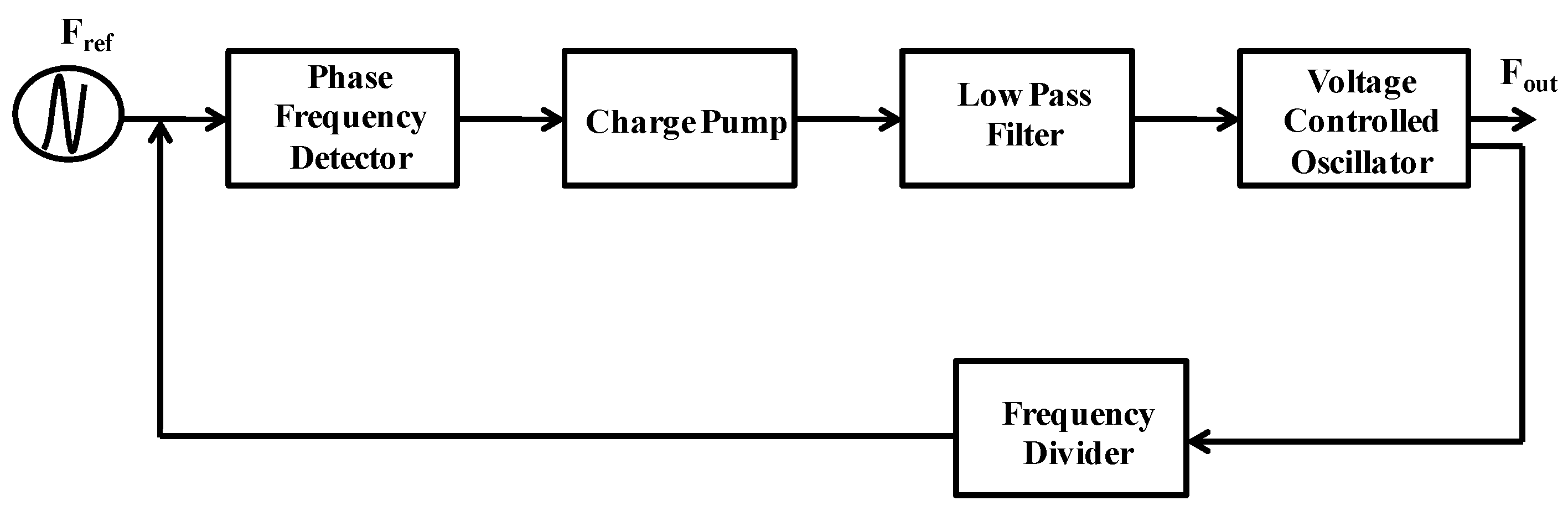
The current era is all about compact battery devices used in electronic devices. A PLL is used in all SOC devices where circuitry generates a system clock signal. Basically, a PLL has a feedback loop that controls the phase of the output signal with the input signal along with phase error.
2. Methodology
Previously, a multiplier was used as an analog phase detector, but it had a limited blocking range with a phase error of more than 90° where the output voltage is reduced. A digital phase detector was implemented where the mean value is proportional to the phase error [2]. The X-OR gate was used as a phase detector, which is linear, but if it were in phase and the error was greater than 180°, it would lose its linearity. Consequently, the phase-frequency detectors are designed to detect phase and frequency differences, which increases the speed of PLL. For the LPF design, first order filter could be used, but it would introduce ripples as the control voltage jumps high when current is injected from the charge pump. To solve this problem, a second-order low-pass filter was designed to suppress the generated ripple. Firstly, VCOs (Voltage Controlled Oscillators) were designed using LC oscillators or ring oscillators [3]. However, ring oscillators are not stable as they let the switching characteristics of logic gates fluctuate by +/−20% and the disadvantage of LC oscillators has more matrix area. Therefore, the current starved VCOs are realized in our proposed design.
The PLL works in three states: Free Running state, Capture state, and Phase Lock state. As the name suggests, the free-running state refers to the phase in which no input voltage is present. As soon as the input frequency is applied, the VCO starts switching and starts producing an output frequency to be compared, and this stage is called the capture state [4].
The frequency comparison stops as soon as the output frequency equals the input frequency. This phase is known as the phase-locked state. PLL is a convenient circuit block widely used in wireless applications and electronics, from cell phones to radios, televisions, Wi-Fi routers, areas like FM demodulators, AM demodulators, frequency synthesizers, and more recovery, etc. [5].
3. Design and Implementation
The proposed design of 90 nm PLL was composed using cadence virtuoso and consisted of all the blocks of a Basic PLL. In this design, the number of transistors is reduced when compared to the existing designs in [6]. Due to this, the area is reduced. The reduced transistors also lead to a decreased usage of the power consumption and cost. The design of blocks of the proposed PLL are shown and discussed below.
3.1. Phase Frequency Detector
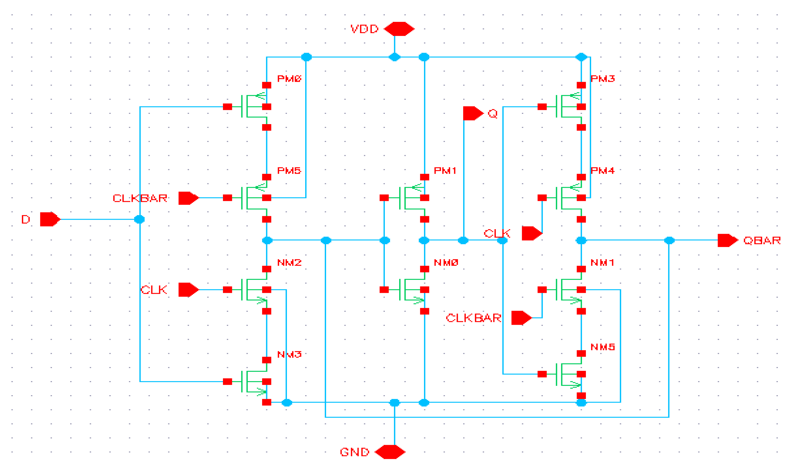
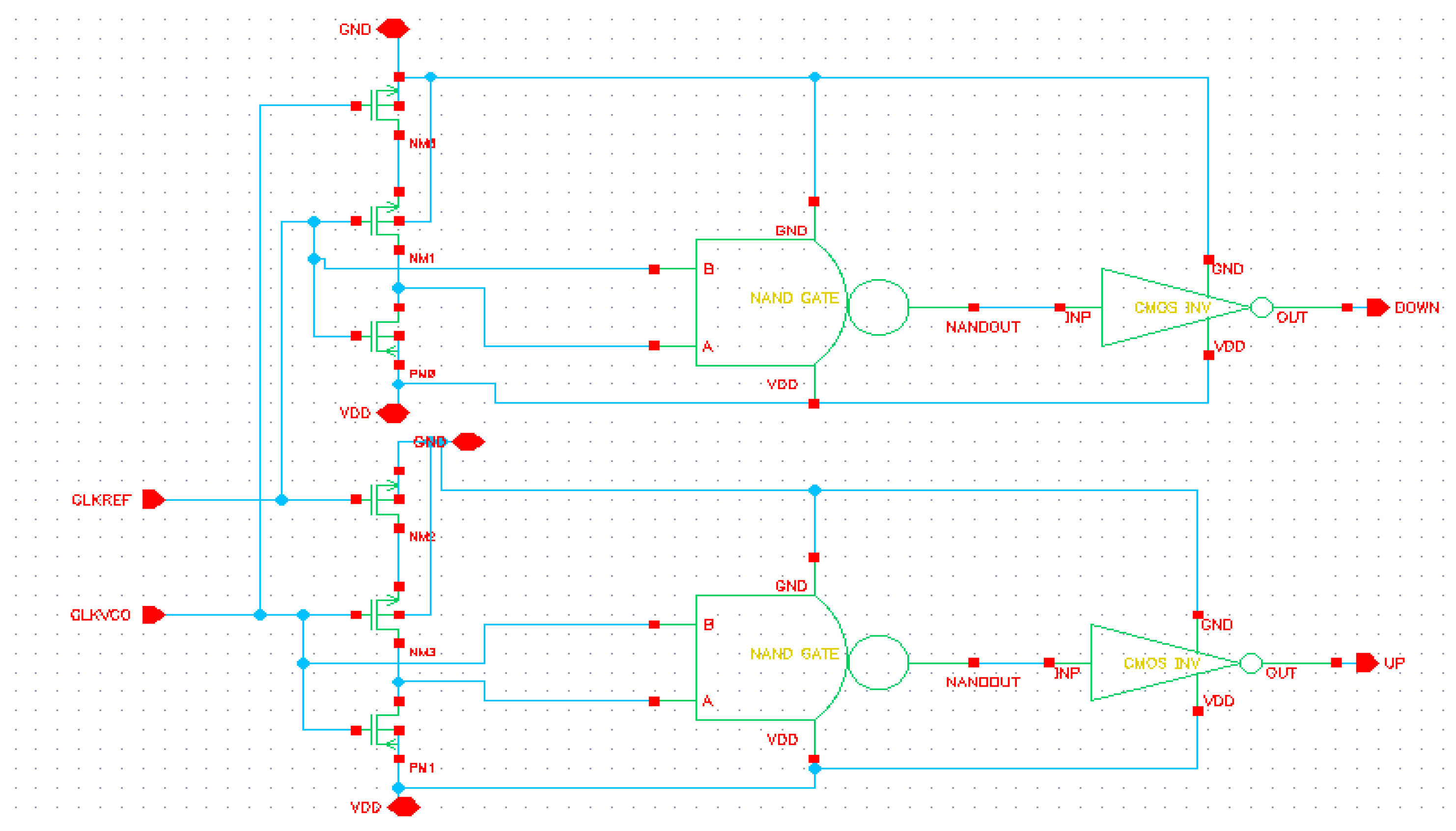
The Phase Frequency Detector (PFD) mainly consists of two D-flip flops and NAND gates. The block diagram of the PFD is shown below in Figure 2. The main purpose of a PFD is to compare the phase and frequency of the input signal with the feedback signal. It has two output signals, UP and DOWN [7].
The design of the low power edge triggered D-Flip flop with 1.8 V is designed with a reduced number of transistors, and the respective output waveforms are shown in Figure 2. This D flipflop has been used in designing the PFD [8].
Figure 3 shows PFD with two input signals, reference signal CLKREF and the feedback signal which is the output of VCO, CLKVCO each as an input to the two D-flipflops. Output of the first D-flipflop enables the positive current source and another the negative current source of the charge pump. Assuming UP=DOWN=0, when CLKREF is high, UP rises thereby CLKVCO rises. When DOWN also is high, NAND gate resets both the D-flipflops. UP and DOWN are high at the same time for a short while, at this point the difference between their average values gives us the phase or frequency difference between both the input signals [9].
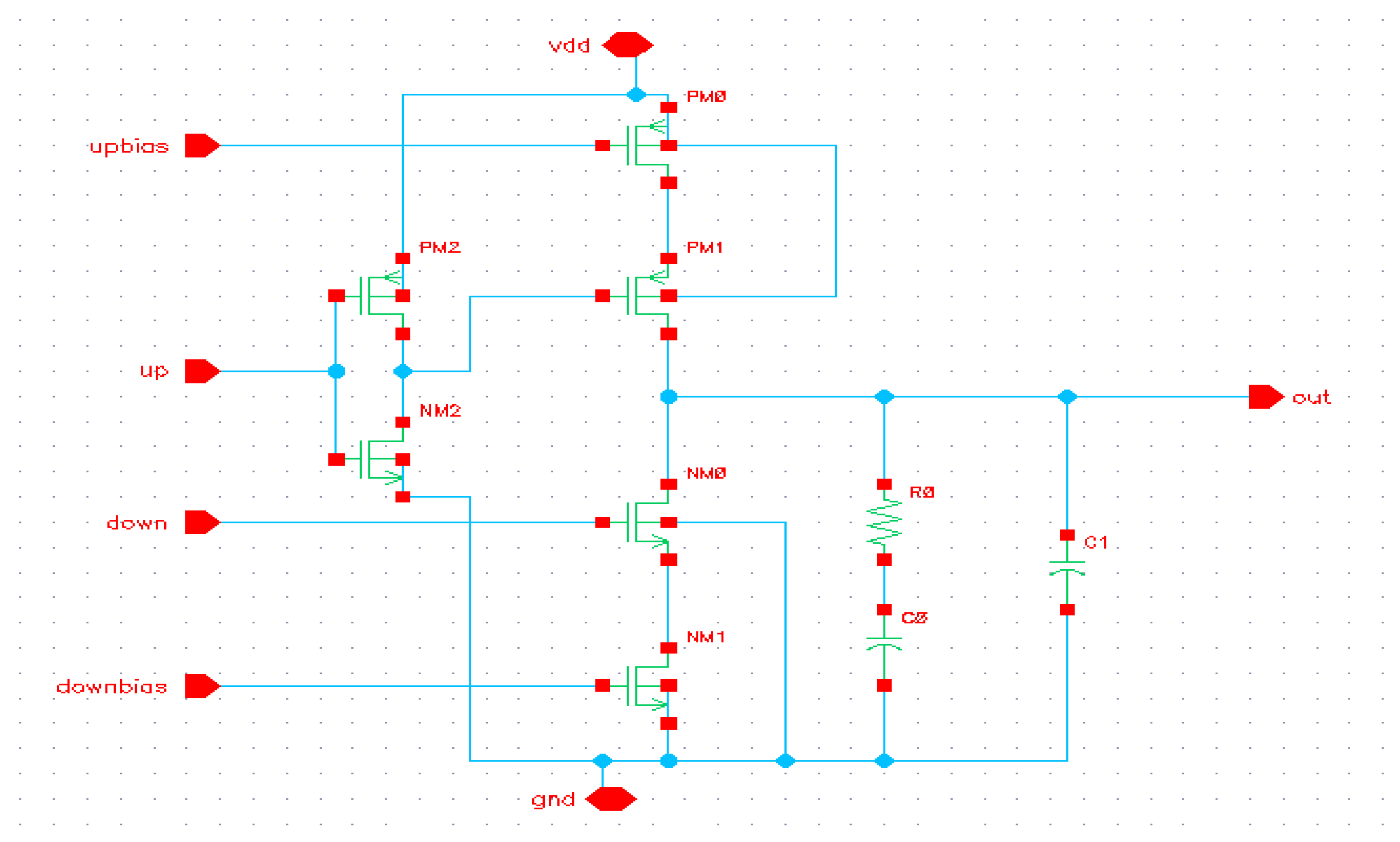
3.2. Charge Pump and Low Pass Filter
The charge pump block in Figure 4 converts the output signals of PFD block i.e., UP and DOWN signals into a voltage that controls the VCO or Vcontrol. This block also gives a constant voltage to hold the VCO at as the loop locks in at a particular frequency. When the UP signal is high, the positive current IPDI flows through the circuit and increases the control voltage, When the downstream signal goes high, a negative IPDI current flows through the circuit, which reduces the control voltage [10]. The output current of the charge pump is given below Equation (1):
where,
The control voltage of VCO is given in Equation (2):
The Low Pass Filter converts the charge pump current into voltage and the frequency of the VCO depends on the output of the LPF. When the charge pump current is positive, the oscillation frequency increases, otherwise it decreases [11]. Figure 4 shows the implementation of Charge Pump along with Low Pass Filter. Low Pass Filter here is important because it filters out higher frequencies and influences the speed of the circuit [12].
3.3. Voltage Controlled Oscillator
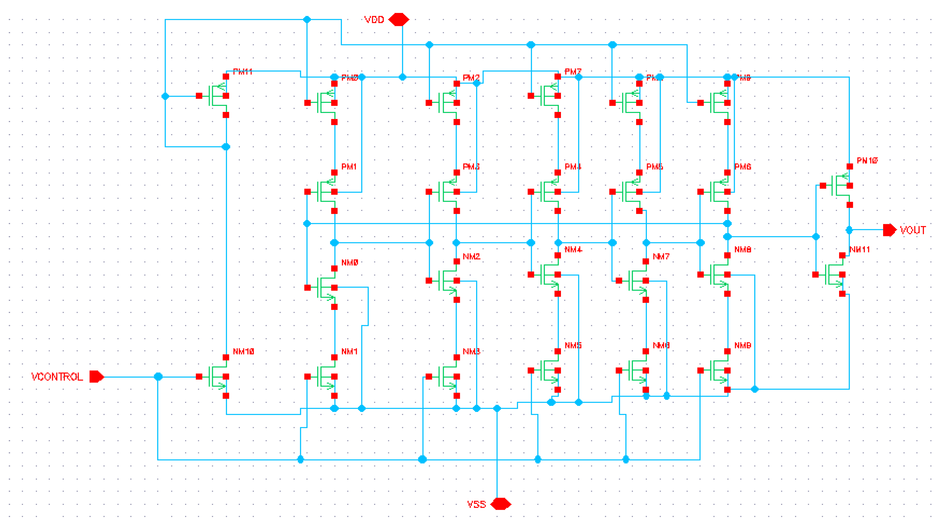
The implementation of a low current VCO circuit that is like a simple ring oscillator with an PMOS and NMOS transistor is done [13]. This limits the current that passes through each inverter, and is thus named a low current VCO. The transistors act as current source sand limit the current to the inverter and the inverter in the next stage is even more starved. This reduced the frequency due to reducing available current and increasing their time to charge and recharge [14]. The schematic of CSVCO is shown in Figure 5.
3.4. Frequency Divider
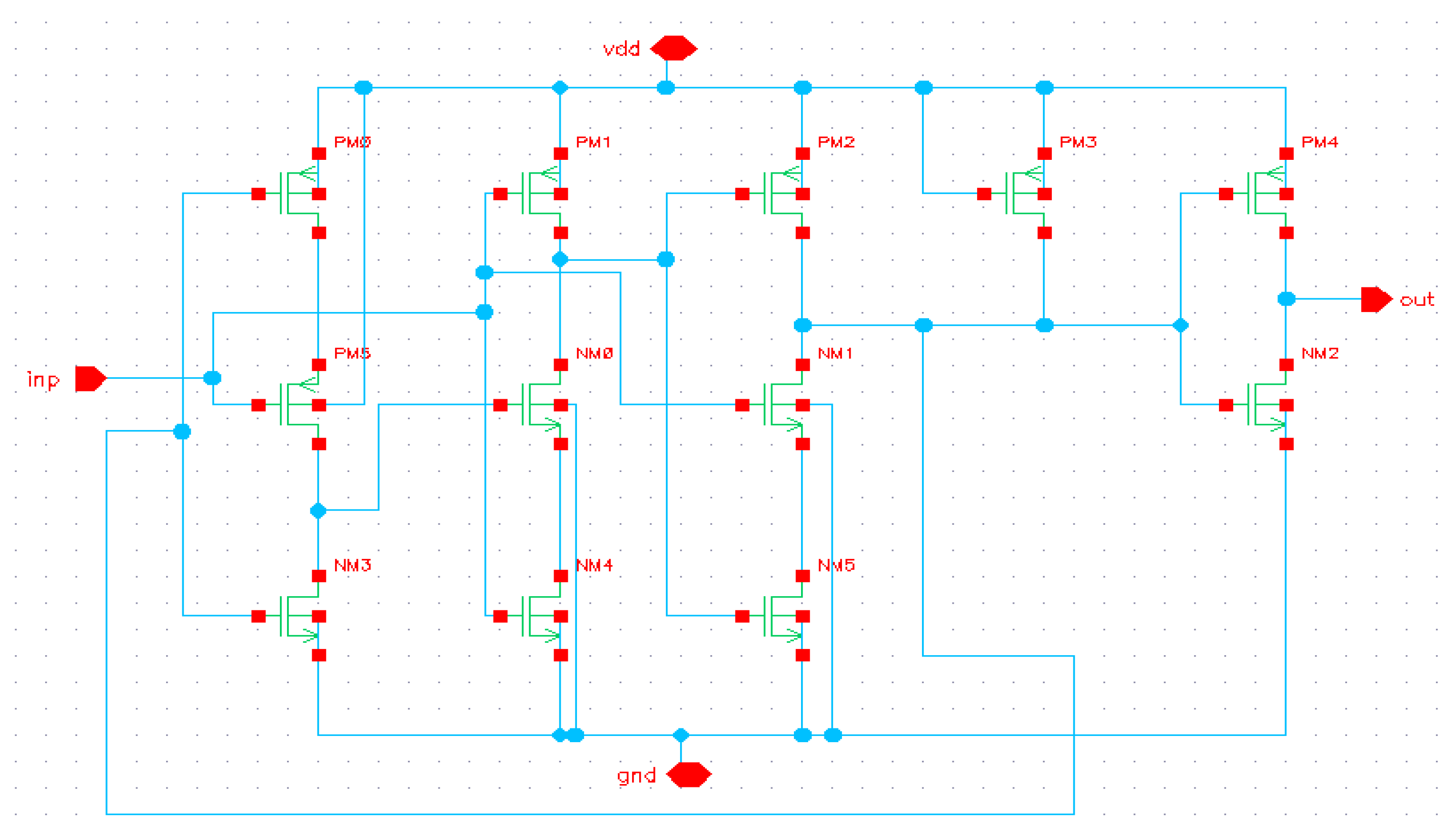
The output of the VCO is provided to the PFD via the frequency divider circuit. The frequency of the VCO output signal is divided by two by this frequency divider block [15]. Two D flipflops constructed using 5 NMOS and 5 PMOS transistors are used to implement the divider circuit, as shown in Figure 6.
4. Results and Observations
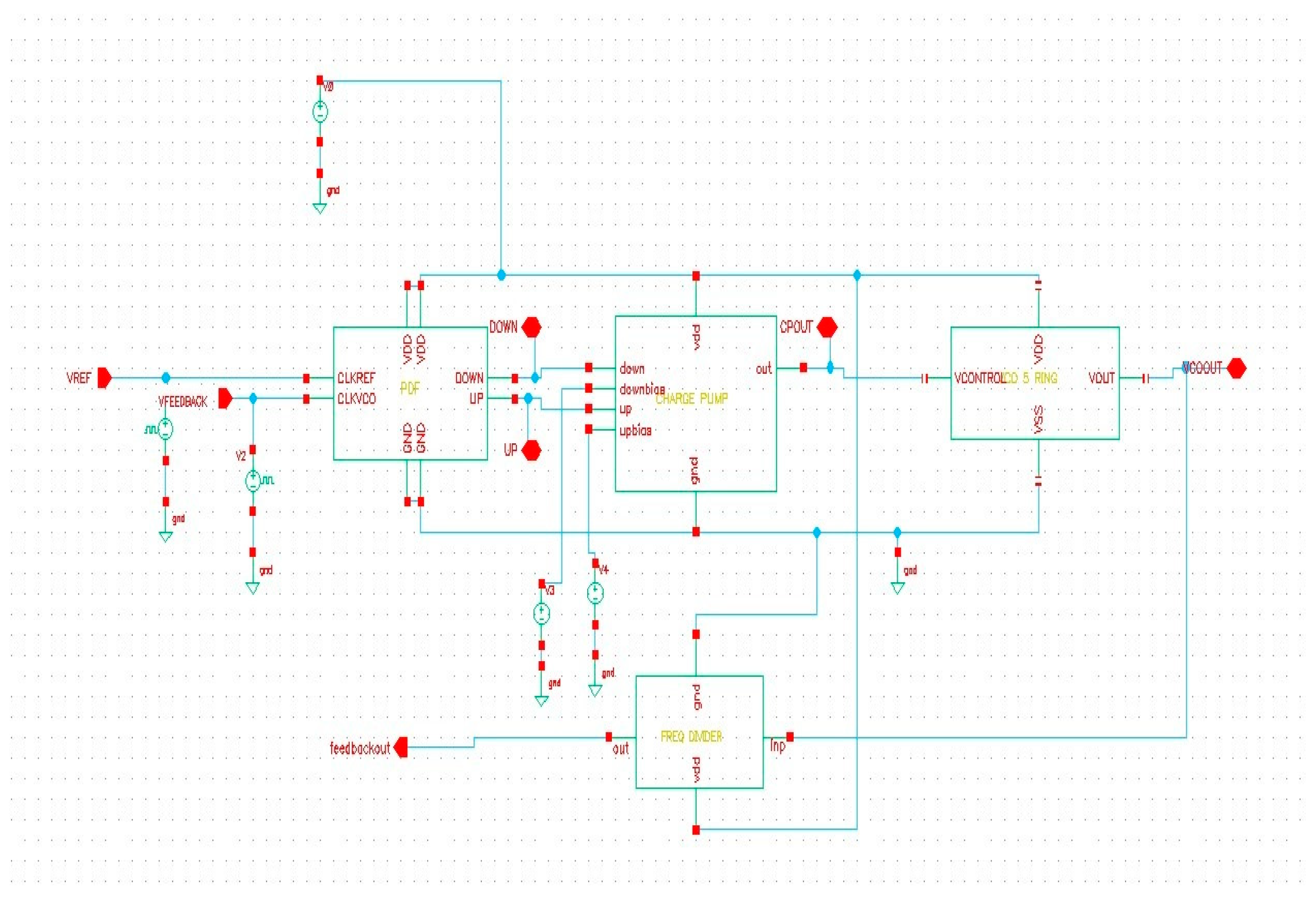
The design of a PLL is done in cadence virtuoso tool by Analog design environment using 90nm node. Here, the transient and DC analysis of proposed PLL and its blocks are discussed. A reference signal and a clock feedback signal are given as input to the PFD with output as UP and DOWN Signals. The output of the charge pump is given to the VCO, which acts as a Voltage control signal, and the output of VCO is given to a Frequency Divider where the output frequency is N/2, which is the feedback signal given back to PFD. Figure 7 shows the entire design of PLL schematic while Figure 8 shows the transient and DC analysis of the same.
Here, in Figure 7 the use of a novel design for PFD and a charge pump is used for reducing the power usage of whole system and it also shows how they are incorporated in the entire PLL.
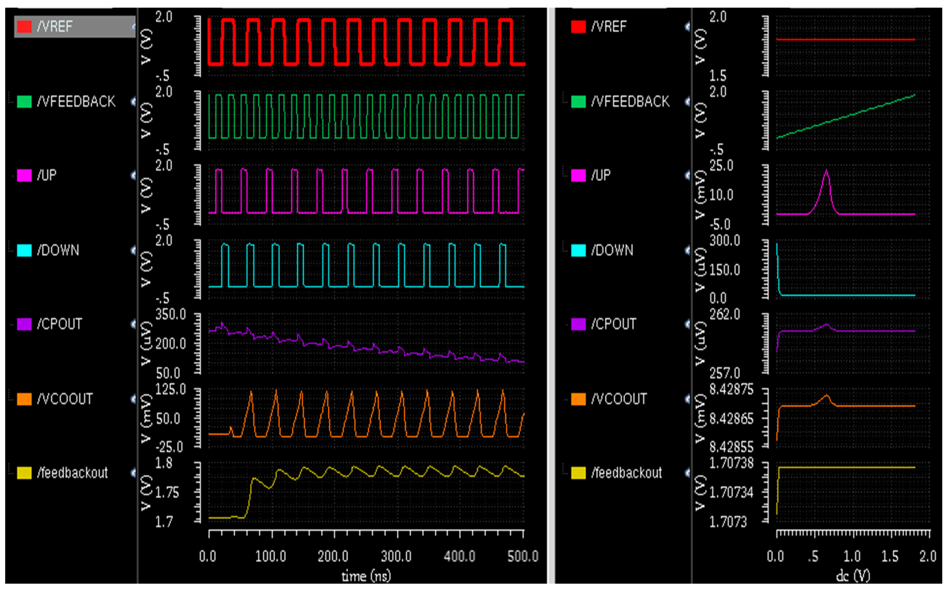
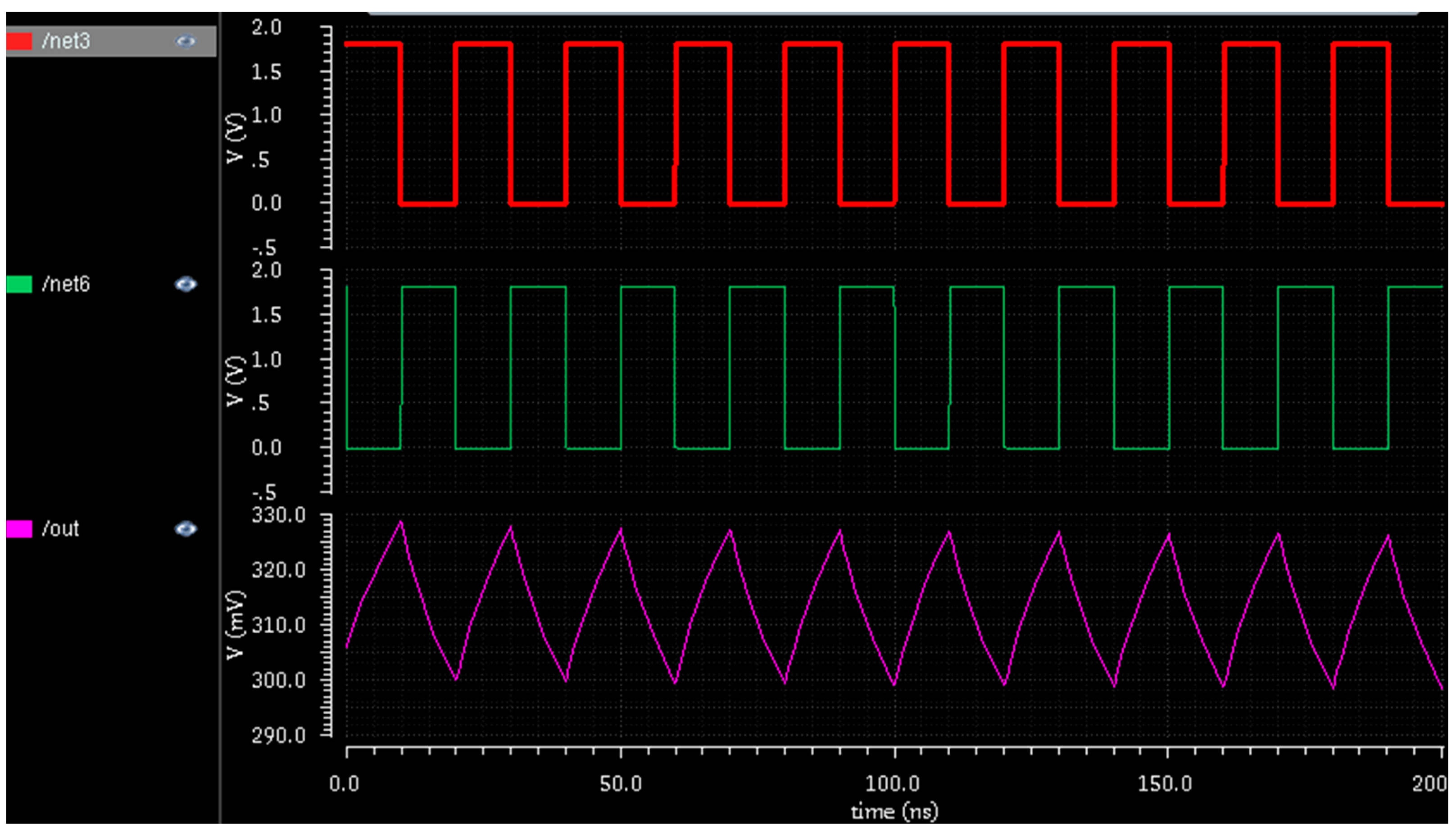
Figure 8 shows transient and DC analysis of the proposed PLL that verifies the working of the PLL in an effective way. This not only shows the output PFD, i.e., UP and DOWN signals that act according to the clock signal but also show the output waveforms of the charge pump which varies according to the input signals. When both the input signals i.e., REF and FEEDBACK are high, the output of the charge pump is high; when both the input signals are low, there is a drop at the output signal of the charge pump, which is given as input to the VCO.
Figure 9 shows the two input signals to Charge Pump, UP and DOWN signals red and green respectively which are observed to be inverse of each other. The output signal of Charge Pump is in purple as OUT signal which is given as the input to the VCO as control signal.
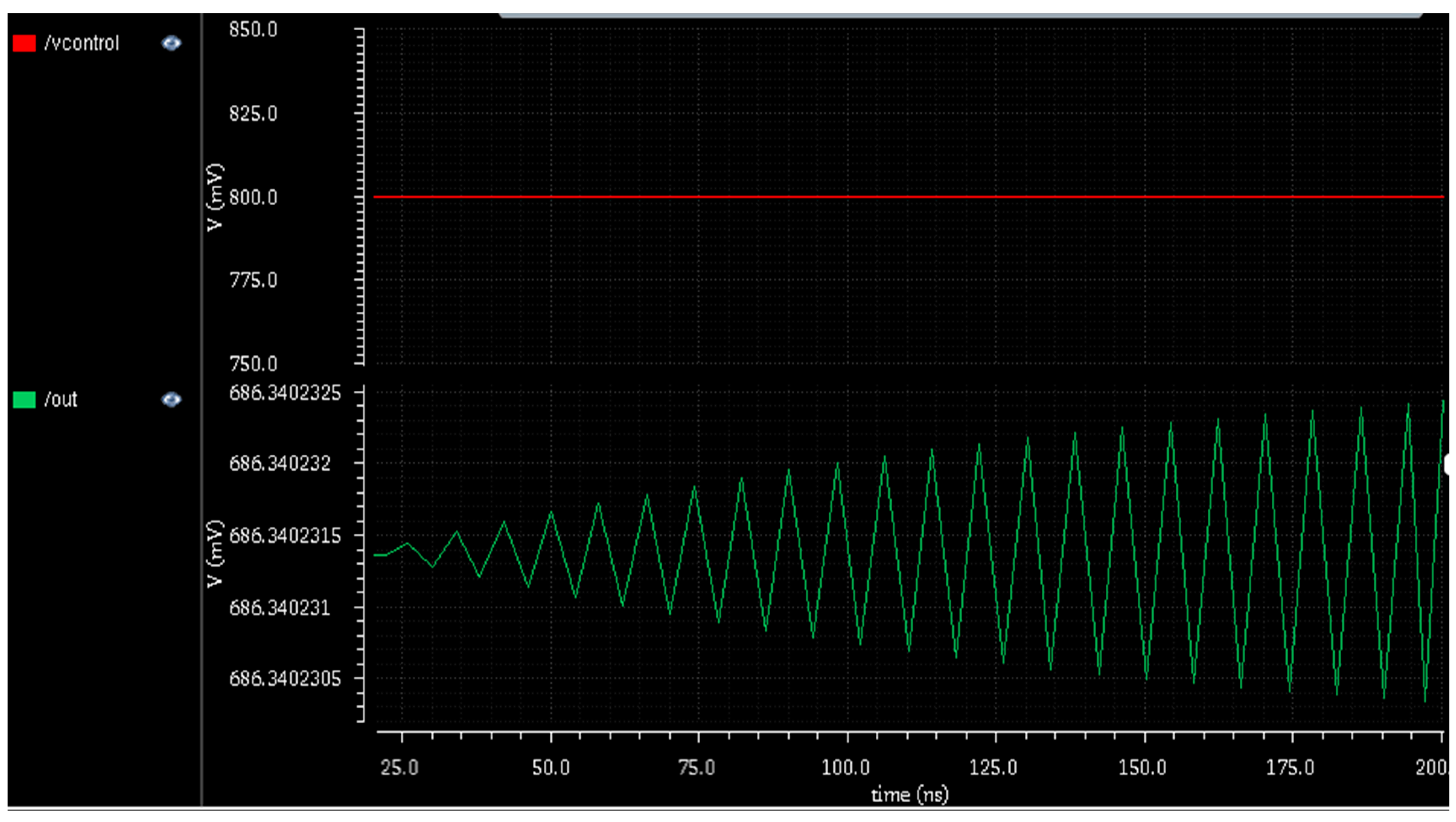
The output waveforms of VCO are shown in Figure 10 with respect to the input control signal. It shows the frequency of the signal produced by VCO at a constant voltage of Vcontrol = 800 mV.
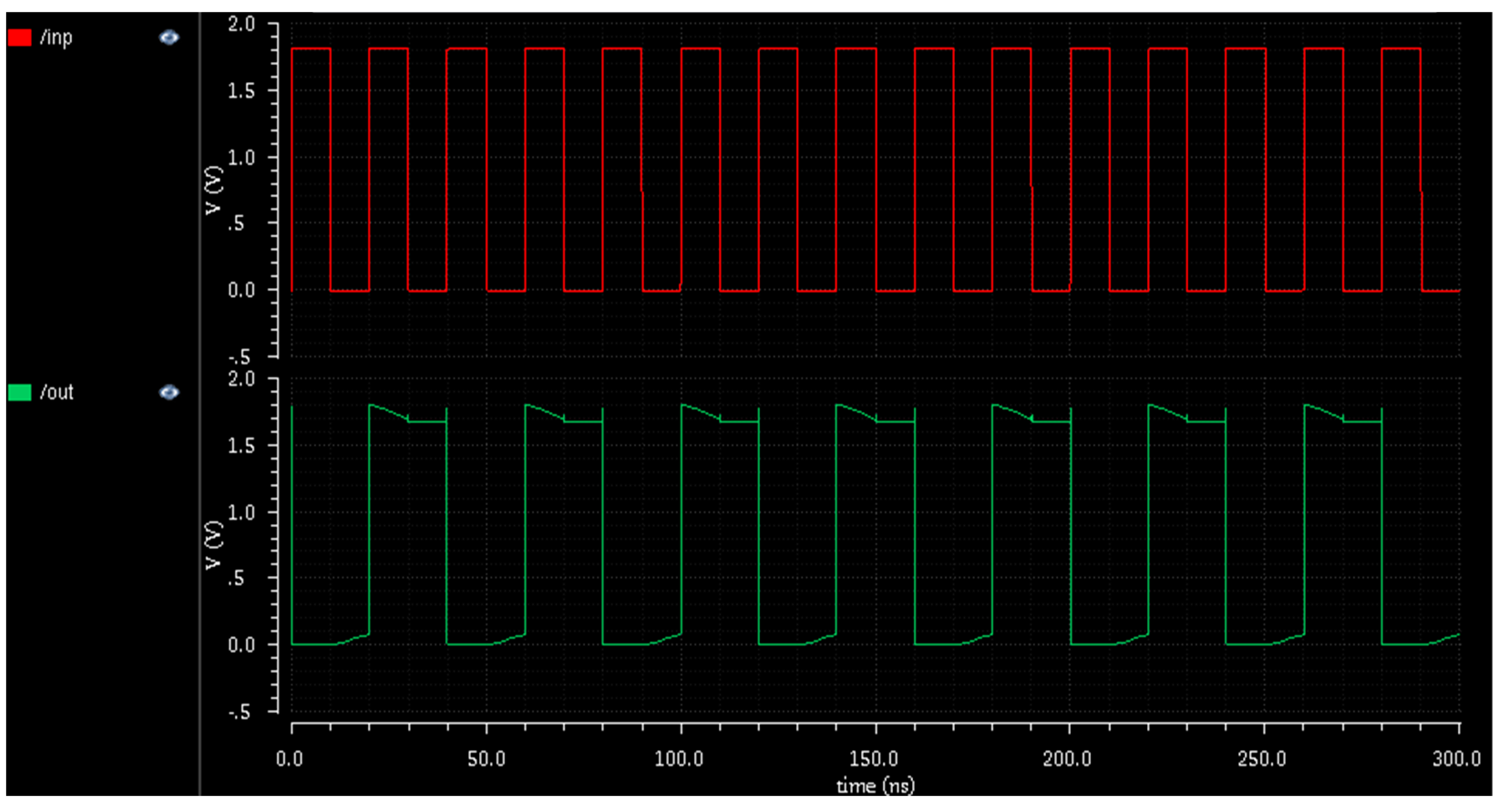
Figure 11 shows input and output of the frequency divider. Visibly, the output pulses have half the frequency of the input pulses. In other words, the input frequency is divided by the frequency divider by a factor of 2.
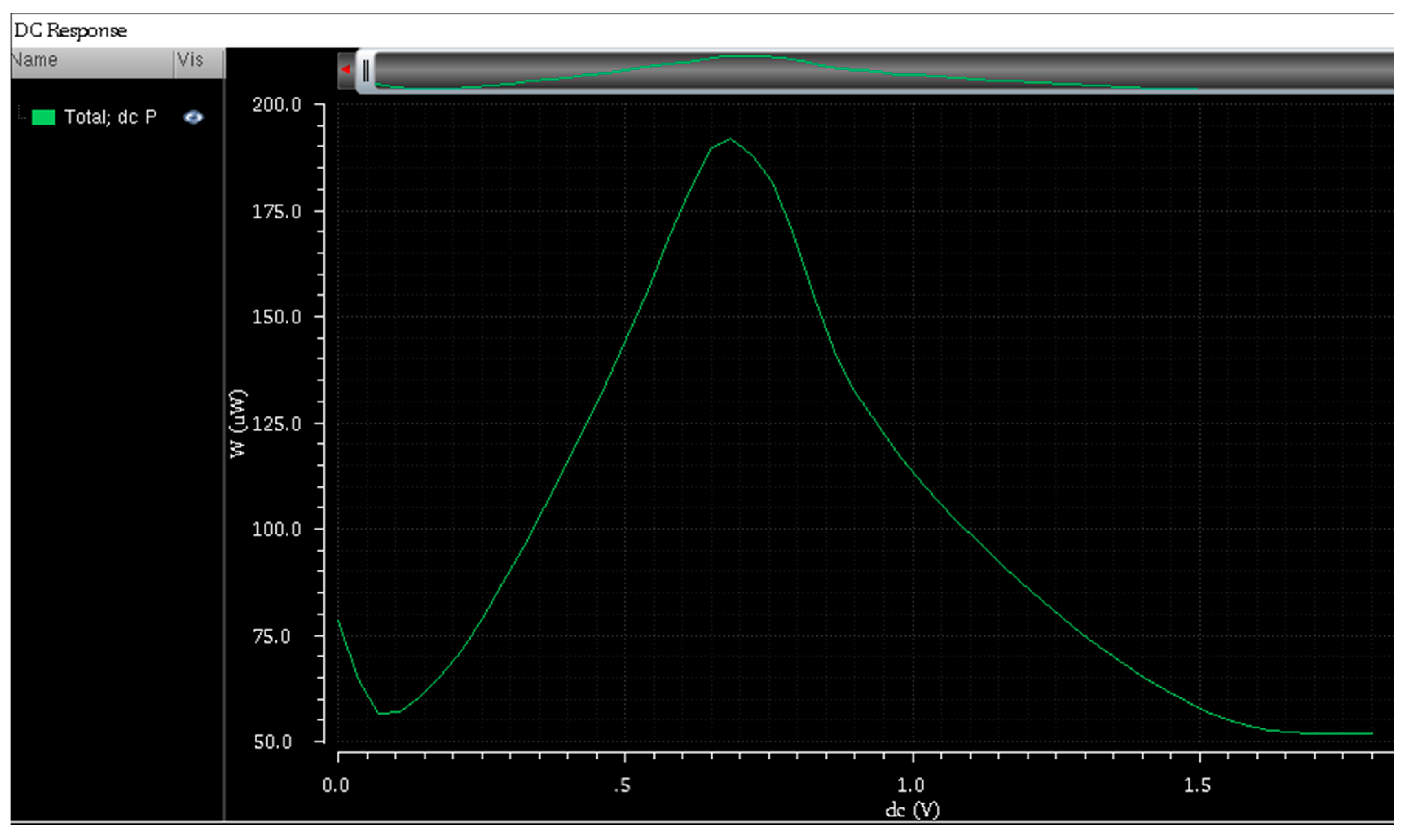
The DC total power analysis plot of the PLL is shown below Figure 12. The graph peaks at 194.24 µW which shows the total power consumption of the PLL circuit.
The results of the proposed work are better than the results of conventional state-of-the-art PLL design in terms of power consumption and the number of transistors used to design PLL, where power consumption is many times less than that of the conventional PLL. The comparative analysis of various parameters is presented in Table 1.
Here, the comparative analysis of different parameters is shown. The parameters such as the number of transistors used in design of PLL, supply voltage, and operating frequency power consumed are used to implement PLL, and are analyzed above. From the analysis, the proposed PLL design has a 14% decrease in the number of transistors with a reduced area and 1000 times less power consumption. So, the proposed PLL can be effectively used in low power digital electronic applications and compact devices.
5. Conclusions
A design of PLL using a cadence virtuoso tool in an analog design environment by using GPDK 90nm technology with 1.8 V DC supply is performed. The simulation work presents a reduced number of transistors with a reduced area in proposed design with very low power consumed at DC voltage of 1.8 V. The Total Power Consumed by the proposed PLL design is 194.24micro-Watts. We know that the power consumed, the sizing of the transistors, and the selection of the power supply voltage at different levels may vary with the total power consumed, respectively. This not only allows the working of PLL at high speed, but also supports working at low power, which makes it very effective for low power applications.
Author Contributions
Conceptualization, C.K.P. and C.S.; methodology, N.P.S.; software, C.K.P.; validation, C.S. and M.R.K.; data curation, J.L.P.; writing—original draft preparation, C.K.P.; writing—review and editing, C.K.P., N.P.S., J.L.P., C.S. and M.R.K.; visualization, N.P.S.; supervision, C.S.; project administration, M.R.K. All authors have read and agreed to the published version of the manuscript.
Funding
This research received no external funding.
Institutional Review Board Statement
Not applicable.
Informed Consent Statement
Not applicable.
Data Availability Statement
Data can be shared on request.
Conflicts of Interest
The authors declare no conflict of interest.
References
- Wang, H.; Momeni, O. A charge pump current mismatch compensation design for sub-sampling PLL. IEEE Trans. Circuits Syst. II Express Briefs 2021, 68, 1852–1856. [Google Scholar] [CrossRef]
- Tsai, T.-H.; Sheen, R.-B.; Chang, C.-H.; Hsieh, K.C.-H.; Staszewski, R.B. A Hybrid-PLL (ADPLL/Charge-Pump PLL) Using Phase Realignment With 0.6-us Settling, 0.619-ps Integrated Jitter, and −240.5-dB FoM in 7-nm FinFET. IEEE Solid-State Circuits Lett. 2020, 3, 174–177. [Google Scholar] [CrossRef]
- Chae, U.; Park, J.; Kim, J.-G.; Yu, H.-Y.; Cho, I.-J. CMOS voltage-controlled oscillator with high-performance MEMS tunable inductor. Micro Nano Syst. Lett. 2021, 9, 13. [Google Scholar] [CrossRef]
- Bamigbade, A.; Khadkikar, V.; Hosani, M.A. A Type-3 PLL for Single-Phase Applications. IEEE Trans. Ind. Appl. 2020, 56, 5533–5542. [Google Scholar] [CrossRef]
- Sánchez-Herrera, R.; Andújar, J.M.; Márquez, M.; Mejías, A.; Gómez-Ruiz, G. Self-Tuning PLL: A New, Easy, Fast and Highly Efficient Phase-Locked Loop Algorithm. IEEE Trans. Energy Convers. 2022, 37, 1164–1175. [Google Scholar] [CrossRef]
- Patil, P.; Ingale, V. Design of a Low Power PLL in 90 nm CMOS Technology. In Proceedings of the IEEE 5th International Conference for Convergence in Technology, Bombay, India, 29–31 March 2019. [Google Scholar]
- Mazza, G.; Panati, S. A Compact, Low Jitter, CMOS 65 nm 4.8–6 GHz Phase-Locked Loop for Applications in HEP Experiments Front-End Electronics. IEEE Trans. Nucl. Sci. 2018, 65, 1212–1217. [Google Scholar] [CrossRef]
- Ghasemian, M.S.P.H. A straightforward quadrature signal generator for single-phase SOGI-PLL with low susceptibility to grid harmonics. IEEE Trans. Ind. Electron. 2021, 69, 6997–7007. [Google Scholar]
- Razavi, B. Jitter-power trade-offs in PLLs. IEEE Trans. Circuits Syst. I Regul. Pap. 2021, 68, 1381–1387. [Google Scholar] [CrossRef]
- Gong, H.; Wang, X.; Harnefors, L. Rethinking current controller design for PLL-synchronized VSCs in weak grids. IEEE Trans. Power Electron. 2021, 37, 1369–1381. [Google Scholar] [CrossRef]
- Hoseinizadeh, S.M.; Ouni, S.; Karimi, H. Comparison of PLL-based and PLL-less vector current controllers. IEEE J. Emerg. Sel. Top. Power Electron. 2021, 10, 436–445. [Google Scholar] [CrossRef]
- Achlerkar, P.D.; Panigrahi, B.K. New perspectives on stability of decoupled double synchronous reference frame PLL. IEEE Trans. Power Electron. 2021, 37, 285–302. [Google Scholar] [CrossRef]
- Lai, W.-C. Performance Improved Voltage Controlled Oscillator and Double Balanced Mixer Chip Design. In Proceedings of the 2021 International Applied Computational Electromagnetics Society (ACES-China) Symposium, Chengdu, China, 28–31 July 2021; pp. 1–3. [Google Scholar]
- Shettar, H.G.; Kotabagi, S.; Shanbhag, N.; Naik, S.; Bagali, R.; Nandavar, S. Frequency Multiplier using Phase-Locked Loop. In Proceedings of the IEEE 17th India Council International Conference (INDICON), New Delhi, India, 10–13 December 2020; pp. 1–5. [Google Scholar]
- Adesina, N.O.; Srivastava, A.; Khan, A.U.; Xu, J. An Ultra-Low Power MOS2 Tunnel Field Effect Transistor PLL Design for IoT Applications. In Proceedings of the Electronics and Mechatronics Conference (IEMTRONICS), Toronto, ON, Canada, 21–24 April 2021; pp. 1–6. [Google Scholar]
Figure 1.
Block diagram of PLL.

Figure 2.
Schematic of D flip flop.

Figure 3.
Schematic of Phase frequency detector.

Figure 4.
Schematic of charge pump with Low Pass Filter.

Figure 5.
Schematic of Voltage controlled oscillator.

Figure 6.
Schematic of the frequency divider.

Figure 7.
Architecture of Proposed PLL.

Figure 8.
Transient analysis and DC analysis of proposed PLL.

Figure 9.
Output Waveforms of Charge Pump.

Figure 10.
Output waveforms of VCO with Vcontrol signal.

Figure 11.
Output wave forms of Frequency Divider.

Figure 12.
The plot of DC total power analysis.


Table 1.
Parametric Analysis.
| Parameters | Traditional PLL | Existing PLL | Proposed PLL |
|---|---|---|---|
| Number of transistors | 112 | 56 | 48 |
| V dd | - | 1.8 V | 1.8 V |
| Operating frequency | - | 1 GHz | 1 GHz |
| Power Consumption | - | 4.2 mW | 194.24 µW |
| Total Power Consumed | High | Medium | low |
| Technology | 180 nm | 90 nm | 90 nm |
Disclaimer/Publisher’s Note: The statements, opinions and data contained in all publications are solely those of the individual author(s) and contributor(s) and not of MDPI and/or the editor(s). MDPI and/or the editor(s) disclaim responsibility for any injury to people or property resulting from any ideas, methods, instructions or products referred to in the content. |
© 2023 by the authors. Licensee MDPI, Basel, Switzerland. This article is an open access article distributed under the terms and conditions of the Creative Commons Attribution (CC BY) license (https://creativecommons.org/licenses/by/4.0/).
Share and Cite
MDPI and ACS Style
Pothina, C.K.; Singh, N.P.; Prasanna, J.L.; Santhosh, C.; Kumar, M.R. Design of Efficient Phase Locked Loop for Low Power Applications. Eng. Proc. 2023, 34, 14. https://doi.org/10.3390/HMAM2-14157
AMA Style
Pothina CK, Singh NP, Prasanna JL, Santhosh C, Kumar MR. Design of Efficient Phase Locked Loop for Low Power Applications. Engineering Proceedings. 2023; 34(1):14. https://doi.org/10.3390/HMAM2-14157
Chicago/Turabian StylePothina, Chandra Keerthi, Ngangbam Phalguni Singh, Jagupilla Lakshmi Prasanna, Chella Santhosh, and Mokkapati Ravi Kumar. 2023. "Design of Efficient Phase Locked Loop for Low Power Applications" Engineering Proceedings 34, no. 1: 14. https://doi.org/10.3390/HMAM2-14157