Review

Field-Effect Sensors Combined with the Scanned Light Pulse Technique: From Artificial Olfactory Images to Chemical Imaging Technologies

by
Tatsuo Yoshinobu
1,*,
Ko-ichiro Miyamoto
2,
Torsten Wagner
3,4 and
Michael J. Schöning
3,4,*
1
Department of Biomedical Engineering, Tohoku University, Sendai 980-8579, Japan
2
Department of Electronic Engineering, Tohoku University, Sendai 980-8579, Japan
3
Institute of Nano- and Biotechnologies, Aachen University of Applied Sciences, 52428 Jülich, Germany
4
Institute of Biological Information Processing (IBI-3), Forschungszentrum Jülich GmbH, 52425 Jülich, Germany
*
Authors to whom correspondence should be addressed.
Chemosensors 2024, 12(2), 20; https://doi.org/10.3390/chemosensors12020020
Submission received: 28 November 2023 / Revised: 19 January 2024 / Accepted: 24 January 2024 / Published: 28 January 2024

Abstract

:
The artificial olfactory image was proposed by Lundström et al. in 1991 as a new strategy for an electronic nose system which generated a two-dimensional mapping to be interpreted as a fingerprint of the detected gas species. The potential distribution generated by the catalytic metals integrated into a semiconductor field-effect structure was read as a photocurrent signal generated by scanning light pulses. The impact of the proposed technology spread beyond gas sensing, inspiring the development of various imaging modalities based on the light addressing of field-effect structures to obtain spatial maps of pH distribution, ions, molecules, and impedance, and these modalities have been applied in both biological and non-biological systems. These light-addressing technologies have been further developed to realize the position control of a faradaic current on the electrode surface for localized electrochemical reactions and amperometric measurements, as well as the actuation of liquids in microfluidic devices.

1. Introduction

The concept of an artificial olfactory image was proposed by Lundström et al. in 1991 [1]. Following the discovery of the sensitivity of a Pd-gate metal–oxide–semiconductor (MOS) transistor to hydrogen in 1973, Prof. Ingemar Lundström paved the way for the realization and understanding of various gas sensors based on field-effect structures with catalytic metal gates and their applications to sensor arrays, electronic noses, and artificial olfactory images [2,3].
An artificial olfactory image is an image generated by a field-effect sensor device to be classified by pattern recognition to identify the composition of the gas sample under testing. From a technical point of view, it is realized by combining two technologies: a catalytic field-effect device, which generates a potential difference in response to the gas, and the scanned light pulse technique (SLPT) [4], which reads the two-dimensional distribution of the surface potential in the field-effect structure.
In some contexts, the artificial olfactory image is said to be the first example of a two-dimensional extension of the light-addressable potentiometric sensor (LAPS) proposed by Hafeman et al. in 1988 [5], a chemical sensor based on a mechanism of signal generation similar to that of the SLPT. It should be noted, however, that an artificial olfactory image does not carry information on the spatial distribution of the analyte. Unlike other imaging technologies based on a LAPS [6,7,8,9], in which the obtained image represents a map of the spatial distribution of the analyte, an artificial olfactory image is not a spatial map but a fingerprint of the gas. Despite this essential difference, the feasibility of image generation demonstrated in [1] inspired and promoted, directly and indirectly, the development of various chemical imaging technologies based on a semiconductor field-effect structure scanned by a light beam.
In this review, both the ascendants and the descendants of an artificial olfactory image, i.e., the technologies that led to it, and the variety of light-addressing technologies that were inspired by or emerged from it, will be summarized and discussed. Table 1 shows the list of light-addressing technologies to be discussed in this review. The following sections first describe how photocurrent generation in a semiconductor can be applied to spatially resolved measurements of ions and gases. Then, the principles and applications of the two-dimensional imaging of chemical species and impedance based on light-addressing technologies will be addressed. Further developments of light-addressing technologies beyond potentiometry—those applied to electrochemistry and actuation—will also be discussed.

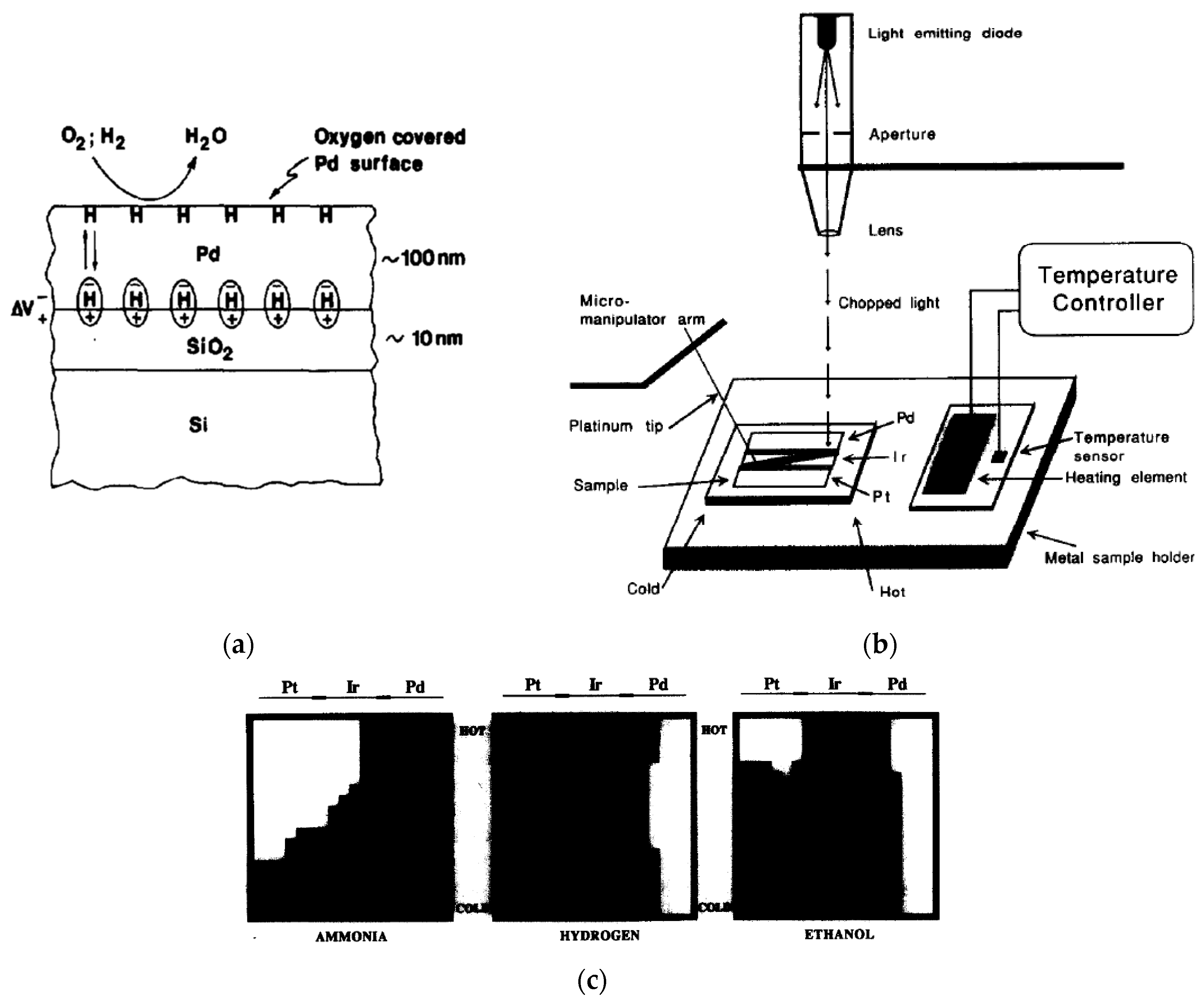
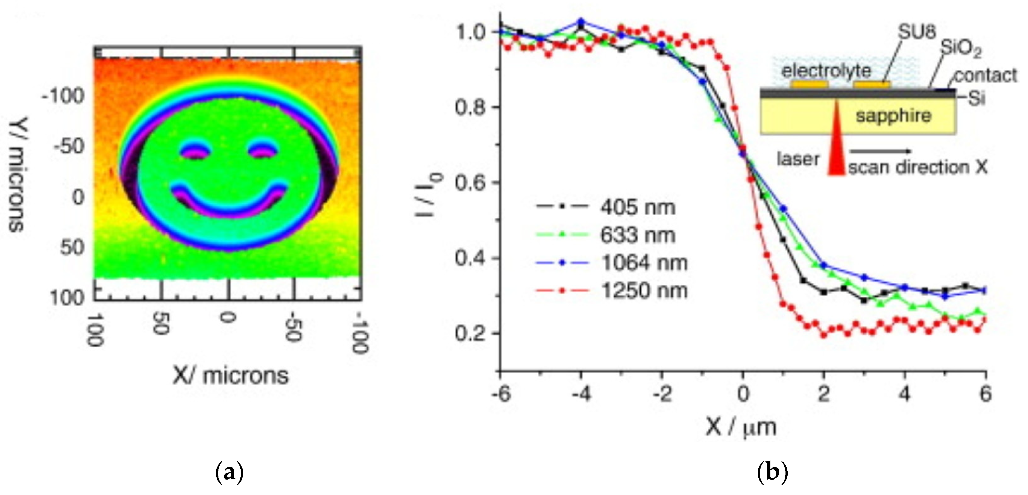
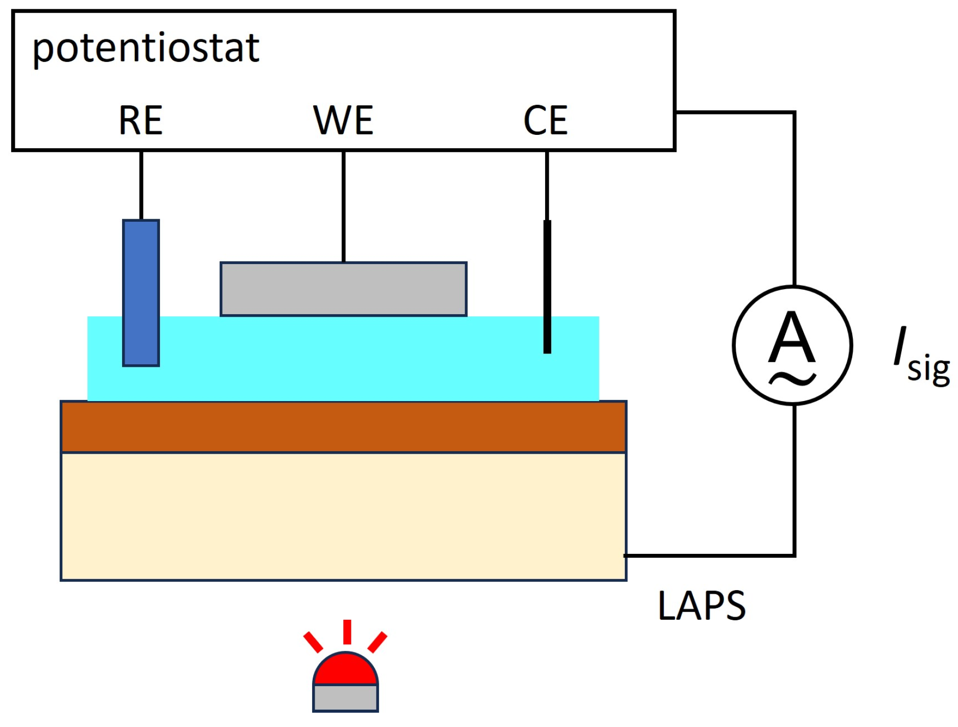
2. From SLPT to LAPS and Artificial Olfactory Images—How It Started

The SLPT is a method to visualize two-dimensional distributions of interface properties, such as the flat-band voltage and the interface state density in a metal–insulator–semiconductor (MIS) structure, as shown in Figure 1a [4]. A bias voltage Vbias is applied to the MIS structure so that the majority carriers in the semiconductor layer are driven away from the insulator–semiconductor interface to form a space charge layer (SCL). Under this situation, the semiconductor layer is illuminated with a chopped light beam with a photon energy larger than the bandgap of the semiconductor. When the light is switched on, the electrons and holes generated by the internal photoelectric effect in the semiconductor are separated by the electric field inside the SCL and a transient current flows in the external circuit until a steady state is reached. When the light is switched off, a transient current flows in the reverse direction. The amplitude of this alternating current Isig is recorded in the external circuit as a function of Vbias, and a current–voltage (IsigVbias) curve, as shown in Figure 1b, is obtained at each illuminated position. The amplitude of the current increases with the SCL’s thickness until strong inversion is reached. The in-plane distribution of the flat-band voltage in the MIS structure, for example, can be obtained by recording the horizontal shift in the IsigVbias curve at each position, or equivalently, by recording the change in Isig under a fixed value of Vbias chosen within the transition region of the curve.
The operating principle of a LAPS is closely related to that of the SLPT. As shown in Figure 1c, a LAPS consists of a semiconductor plate covered with an insulator, and its surface is in contact with the solution under test, forming an electrolyte–insulator–semiconductor (EIS) structure, which is common to the gate region of an ion-sensitive field-effect transistor (ISFET) [24]. The surface of the insulator layer serves as the sensing surface, typically by selectively capturing the target ions, which builds up a potential difference Vchem between the solution and the sensing surface, as shown in Figure 1c, depending on the activity of the target species. Since Vchem is in series with the externally applied Vbias, their sum will be the effective bias voltage applied to the EIS structure. The measurement process hereafter is identical to that of the SLPT. The semiconductor layer is illuminated by a chopped light beam and the amplitude of the alternating current Isig is measured as a function of Vbias. The horizontal shift in the IsigVbias curve represents the change in Vchem, which can be translated into the activity or the concentration of the target ion in the solution. Figure 1d shows an example of a shift in the IsigVbias curve of a LAPS that responds to pH changes. As a member of the family of semiconductor-based chemical sensors with a field-effect structure, the LAPS shares many features in common with other such sensors such as the ISFET and capacitive EIS sensor [6]. They have essentially the same response in the surface potential to the activity of target analytes, and the surface modification technologies and materials developed for one can easily be applied to others. In this way, various ions have been measured by a LAPS furnished with ion-selective membranes, and the application of a LAPS to biosensing has also been extensively studied [25,26,27]. For example, enzymes immobilized on a LAPS surface can catalyze a reaction involving the substrate, enabling detection of a pH change. In an affinity-type of biosensing LAPS, the variation in the surface potential due to selective bindings, such as those between antibodies and antigens or even cells, between aptamers and proteins, or between complementary single-stranded DNAs, has been detected successfully.
Artificial olfactory images were realized by applying the SLPT to a gas sensor comprising an MOS structure with a catalytic metal gate [1,2,3]. The history of the development of catalytic field-effect devices, from a hydrogen sensor based on a Pd-gate MOS transistor [28] to electronic noses [29] and artificial olfactory images [1], is described in [3]. In a catalytic field-effect device, the top metal layer in the MOS structure is composed of a catalytic metal, which catalyzes the reaction of the target gas, like hydrogen, on the surface. As a result, a potential difference due to atomic hydrogen is produced at the metal–oxide interface, as shown in Figure 2a [3]. A variation in this potential difference is observed as a change in the flat-band voltage, which can be read by the SLPT. To obtain an artificial olfactory image as a fingerprint of the gas species, different catalytic metals (Pd, Ir, and Pt) were deposited on the surface, and a temperature gradient was formed along one direction of the sensor plate, as shown in Figure 2b [2]. In this way, measurements at different positions on the sensing surface can be carried out under different conditions, and therefore, each pixel on the sensing surface can be regarded as an independent sensor that constitutes a large virtual array of sensors, whose output forms the input to the electronic nose system. Figure 2c shows examples of artificial olfactory images for different gases in air: 100 ppm of ammonia (left), hydrogen (middle), and ethanol (right) [2]. These images can be fed as inputs to an electronic nose system or used to train a machine learning system, such as an artificial neural network (ANN), which will be able to recognize and identify unknown gas samples. In [1], the authors also point out the similarity between the proposed method and the olfactory recognition mechanism in our brain, where the signals from olfactory receptor neurons are once encoded into a two-dimensional image.
Whereas a conventional electronic nose system relying on an array of discrete gas sensors can be bulky, an artificial olfactory image can be recorded with a single sensor chip. In addition, as the sensor chip has a temperature gradient in one direction, the response of each catalytic metal at different temperatures is embedded in an artificial olfactory image. The richness of information to be fed into machine learning is an additional benefit of artificial olfactory images.
Kanai et al. [12] applied the same concept to generate taste images. In this electronic tongue system, five different lipid membranes (oleic acid, lecithin, cholesterol, phosphatidyl-ethanolamine, and dioctyl phosphate) were deposited on the sensing surface, which was brought into contact with the sample solution. Photocurrent images were obtained as fingerprints of taste substances such as NaCl for saltiness, HCl for sourness, quinine-HCl for bitterness, saccharose for sweetness, and sodium glutamate monohydrate for umami, as well as several beverages such as coffee, black tea, and beer. Furthermore, Shimizu et al. [13] applied the same technique to biosensing, integrating photopolymer membranes containing enzymes such as urease and glucose oxidase on the sensing surface. Their response was acquired in the form of photocurrent images, which demonstrated the feasibility of monolithically integrated biosensors with a plurality of enzymes.

3. Further Development of Gas Sensors

Following the successful application of the SLPT to gas sensing in [1], different device structures and materials were tested to explore further possibilities of gas sensors based on a field-effect structure scanned by a light beam. Ito et al. [10] deposited four different gate metals (Pt, Ag, Au, and Ti) on the insulator (SiN and SiO2) surface, and the entire surface was covered by an agarose gel containing KOH and a gas-permeable membrane, as shown in Figure 3a. This structure allowed the use of a reference electrode (RE) to contact the gel, whereas the catalytic metal gates in Figure 2b, which were directly exposed to the gas, required wiring to the external circuit. Sato et al. [30] proposed yet another device structure, as shown in Figure 3b. A planar electrode is placed above the sensing surface with an air gap of about 1 μm in thickness. The gas sample is introduced into this gap, and the alternating current signal flows through the capacitance between the sensing surface and the planar electrode. With this suspended-gate structure, wiring to individual gate metals on the insulator surface is no longer necessary.
Different materials have also been examined for gas sensing. Pecora et al. [11] tested an amorphous silicon-based LAPS for hydrogen sensing. They deposited hydrogenated amorphous silicon (a-Si:H) as a semiconductor layer, hydrogenated amorphous silicon nitride (a-SiN1.6:H) as an insulator layer, and Pd as a catalytic metal gate to construct a gas-sensitive LAPS on a glass substrate and demonstrated its response to hydrogen concentrations down to 10 ppm. Sato et al. [30] demonstrated oxygen gas sensing by depositing LaF3 and Pt on the insulator surface in the suspended-gate structure described above. Absorption of oxygen by LaF3 resulted in a positive surface potential, and a clear response was observed for the partial pressure of oxygen in the range of 0.25–0.75 atm, whereas no response was observed for CO2 or Ar. Yamada et al. [31] reported on gas sensing with an MIS structure of Au/cubic-like mesoporous silica/Si3N4/SiO2/Si and demonstrated its response to 100 ppm NO gas.
The application of artificial olfactory images to the detection of respiratory acetone as a marker of diabetes was proposed by Zhang et al. [32]. They deposited three different metals (Pt, Ag, and NiTi) on a 90 nm thick thermal oxide on Si, formed a temperature gradient in one direction on the sensing surface, and obtained artificial olfactory images in response to 400 ppm of gaseous acetone in a gas flow of nitrogen blown onto the sensing surface.

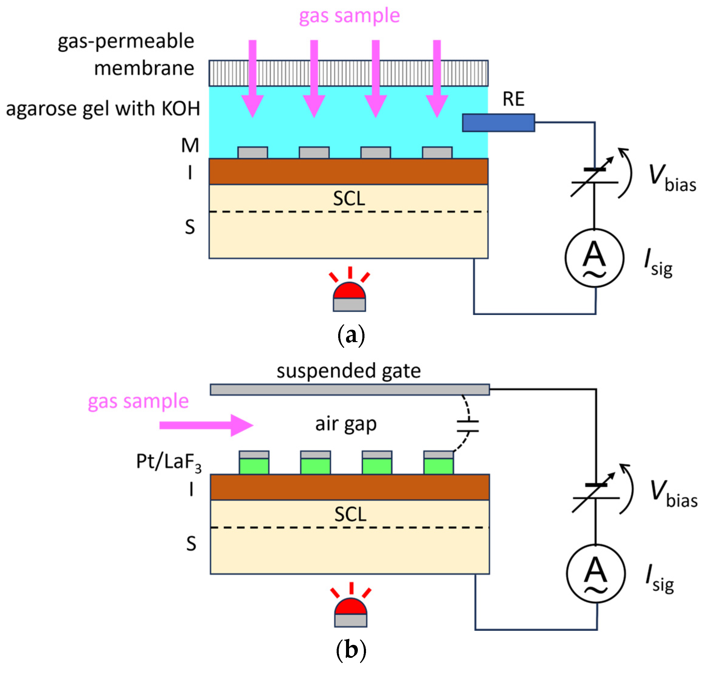
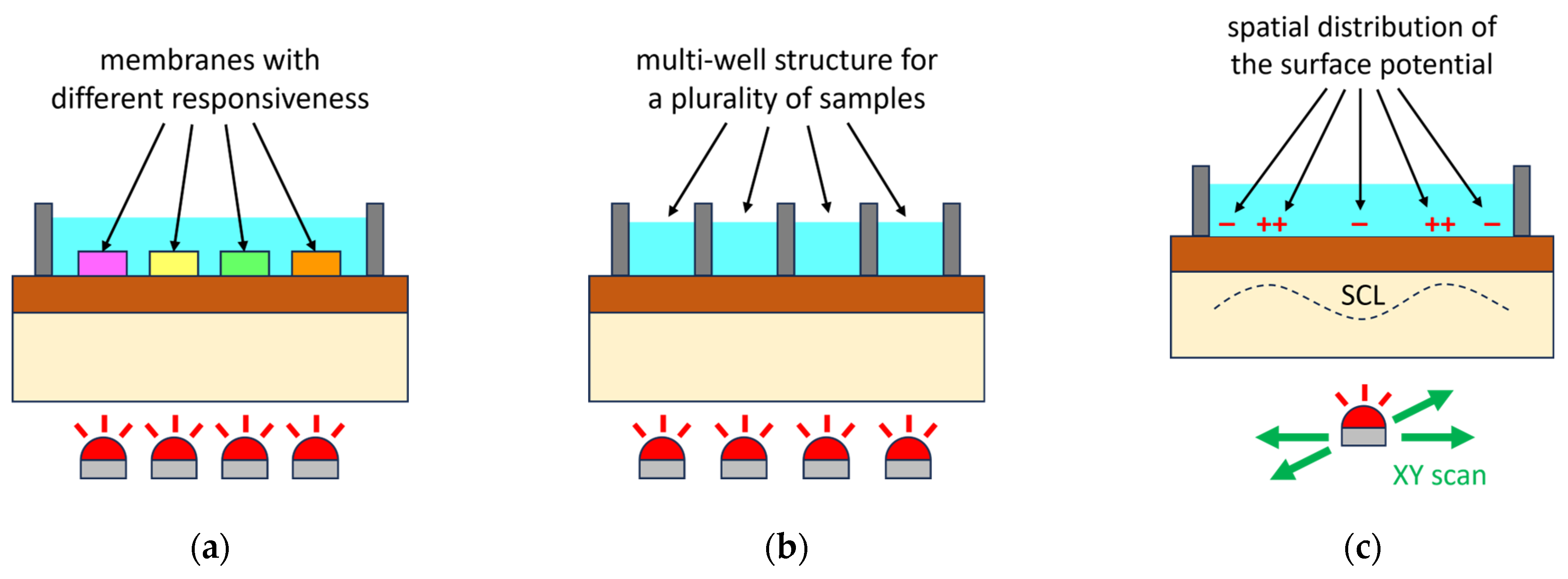
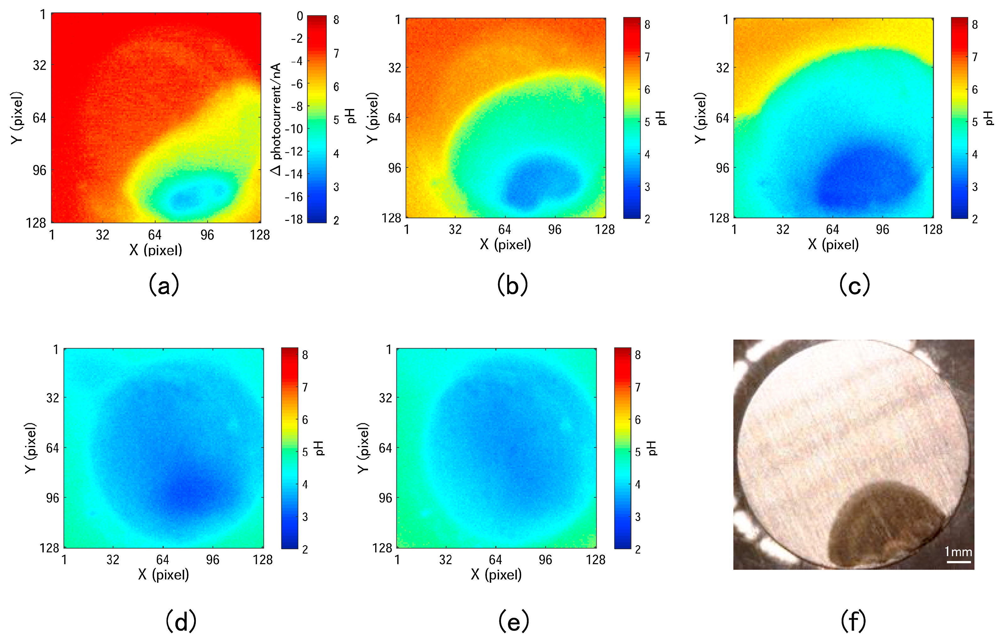
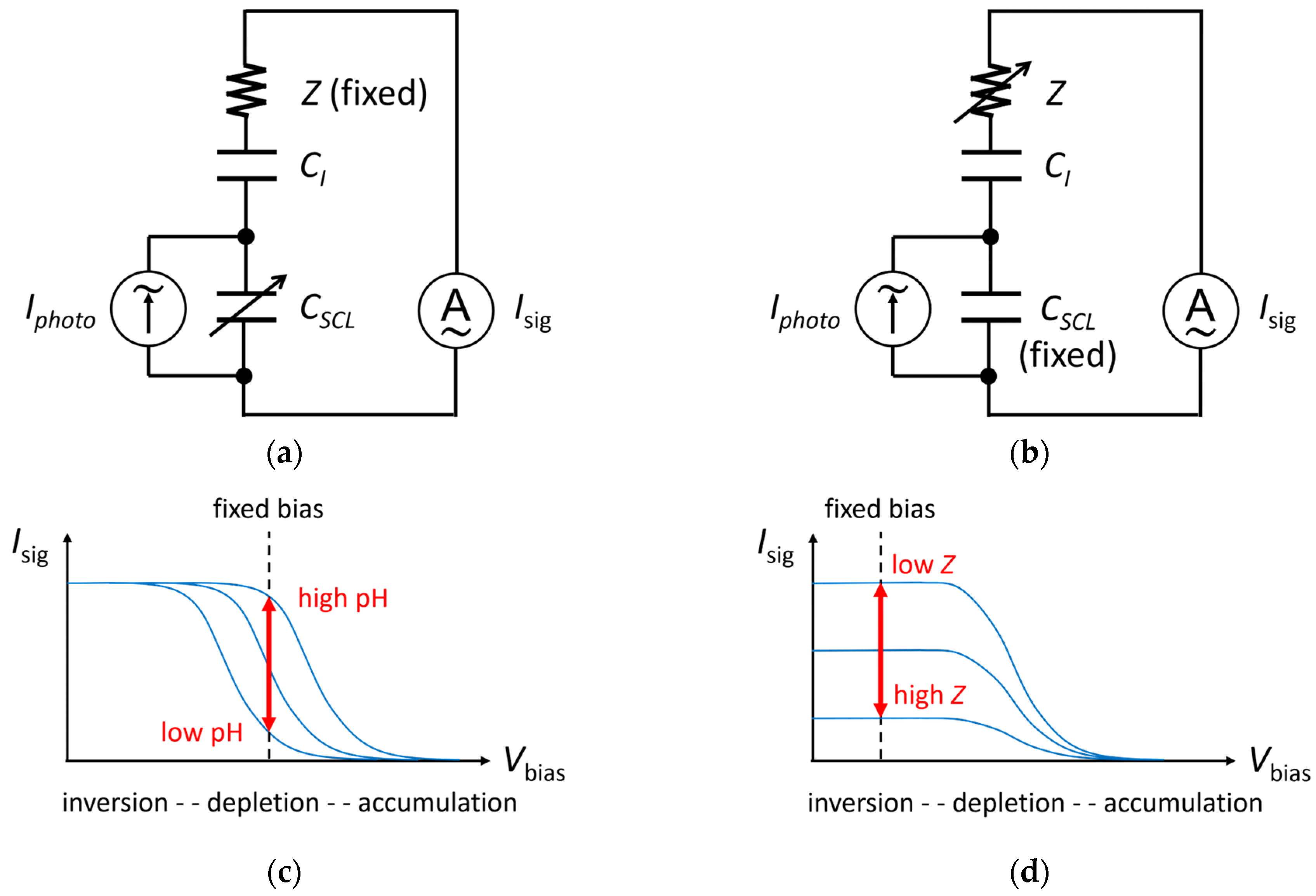
4. Two-Dimensional Maps of Ion Concentration and Impedance

When the LAPS was first introduced [5], its main target was multi-analyte sensing, in which different sensing elements integrated on a single sensor platform, as shown in Figure 4a, were individually accessed by a light beam. A multi-ion LAPS with a plurality of ion-selective membranes (ISM) is a typical example of such a system [33,34].
Among different types of ISMs such as glass membranes, crystalline membranes, and ion-exchange polymer membranes, which were originally developed for ion-selective electrodes for potentiometry, ion-exchange polymer membranes have often been used in multi-ion LAPS systems. This is due to the variety of available ionophores for many cations and anions, as well as the possibility of patterning polymers such as polyvinyl chloride or photocurable resins containing ionophores on the sensing surface. The strategy of the artificial olfactory image [1] also falls into the category of multi-analyte sensing in the sense that different locations on the sensing surface possess different responsiveness.
The second possible form using light-addressability is a multi-well, multi-chamber, or multi-channel structure that can accommodate multiple sample solutions, as shown in Figure 4b [35]. In this configuration, the sensing surface of a single sensor plate can be divided into many sensing areas that function as independent sensors, which is advantageous for handling various samples at high throughput. For example, by replacing the bottom of a 96-well plate with the sensing surface of a LAPS, temporal changes in each well, such as those caused by metabolic activities of cells, can be monitored in parallel.
The third form of measurement utilizing light-addressability is the chemical imaging sensor in which the two-dimensional distribution of the target ions in the vicinity of the sensing surface is visualized. As illustrated in Figure 4c, the surface potential is distributed in response to the local activity of the target ions, which is then reflected in the local thickness of the SCL. By scanning the sensor plate with a chopped light beam and recording Isig at each pixel under a fixed bias condition, as shown in Figure 1d, a photocurrent map is obtained, which can be translated into a spatial map of the activity or the concentration of the target ions. Nakao et al. reported on a pH-imaging sensor system based on this principle [14] and demonstrated that it could visualize acidification due to metabolic activities of microbial colonies [36].
Figure 5 shows an example in which a chemical imaging sensor was applied to the study of corrosion of a metal surface [37].
Stainless steel is a corrosion-resistant material but it is known to corrode rapidly when the surface is confined in a narrow space on the micrometer scale. To study the mechanism of this phenomenon, known as crevice corrosion, a method of probing in such a narrow space is necessary. The surface of a test piece of stainless steel was brought into proximity to the sensing surface, and the spatiotemporal change in pH due to the elution of metal ions and subsequent hydrolysis was recorded by the chemical imaging sensor. Figure 5a–e shows the initiation and development of corrosion accompanied by a pH drop to 2 in the gap. The corroded area observed in the optical image, Figure 5f, of the test piece after the experiment corresponds to the area where the pH value dropped to 2.
Figure 6 presents another example in which a chemical imaging sensor was applied to the quantitative measurement of the metabolic activity of bacteria [38]. Four incubation chambers were formed on the sensing surface, in which different concentrations of bacteria were incubated for 20 min, both with and without glucose. The obtained photocurrent images show the degree of acidification due to the metabolic activities. In this study, the dependence of acidification on the glucose concentration was also measured. Furthermore, the same setup was applied to the measurement of Chinese hamster ovary (CHO) cells, demonstrating that metabolic activities of both bacteria and eukaryotic cells can be quantitatively measured by the proposed method.
Figure 7 highlights an example of a biological application of in vivo pH imaging based on a LAPS [39]. A tiny LAPS chip was attached at the end of an optical fiber bundle (including an integrated Ag/AgCl pseudo reference electrode), which delivered light beams to different locations on the backside of the LAPS chip to acquire the local pH values at the respective locations. The assembly was implanted into the brain of a rat to acquire pH images at a spatial resolution of 250 μm and a temporal resolution of 30 Hz.
Krause et al. [19,40] proposed yet another modality of measurement, scanning photo-induced impedance microscopy (SPIM), based on essentially the same device structure as that of a LAPS. Whereas the LAPS and the chemical imaging sensor respond to the variation in the surface potential, which is a function of the activity of the target species, SPIM responds to the impedance on the sensing surface and generates a spatial map of impedance. Figure 8 compares the simplified circuit models for alternating currents and the IsigVbias characteristics of the LAPS (Figure 8a,c) and SPIM (Figure 8b,d).
In the LAPS-mode operation, the bias voltage is fixed within the transition region of the IsigVbias curve, as shown in Figure 8c. This region corresponds to the state of depletion, where CSCL changes in response to the variation in Vchem, which is a function of the local concentration of the target ions. The photocurrent map obtained in this mode, therefore, represents the spatial distribution of the target ions.
In contrast, the bias voltage in the SPIM-mode operation is fixed in the saturation region of the IsigVbias curve, as shown in Figure 8d, which corresponds to the state of inversion. In this region, the SCL’s thickness no longer changes and CSCL is a constant. As the height of the IsigVbias curve varies depending on Z, the photocurrent map obtained in this mode represents the spatial distribution of the impedance on the sensing surface.
Various efforts have been made to enhance the spatial resolution of the LAPS and SPIM [6]. To obtain a high spatial resolution, the generation of photocarriers by light absorption must be confined in a small area, and the diffusion of photocarriers must be suppressed. Chen et al. [41] reported a submicrometer resolution of LAPS and SPIM using a two-photon effect in Si. They employed a laser beam with a wavelength of 1250 nm to illuminate the backside of a silicon-on-sapphire (SOS) substrate with a thin anodic oxide. The photon energy of the laser beam was smaller than the energy bandgap of Si but more than half of it, and only two-photon absorption occurred. As the rate of two-photon absorption is quadratically dependent on the light intensity, the generation of photocarriers is confined within a sharp focus. Figure 9 shows an example with a high spatial resolution of 0.8 μm realized by the two-photon effect in LAPS and SPIM.

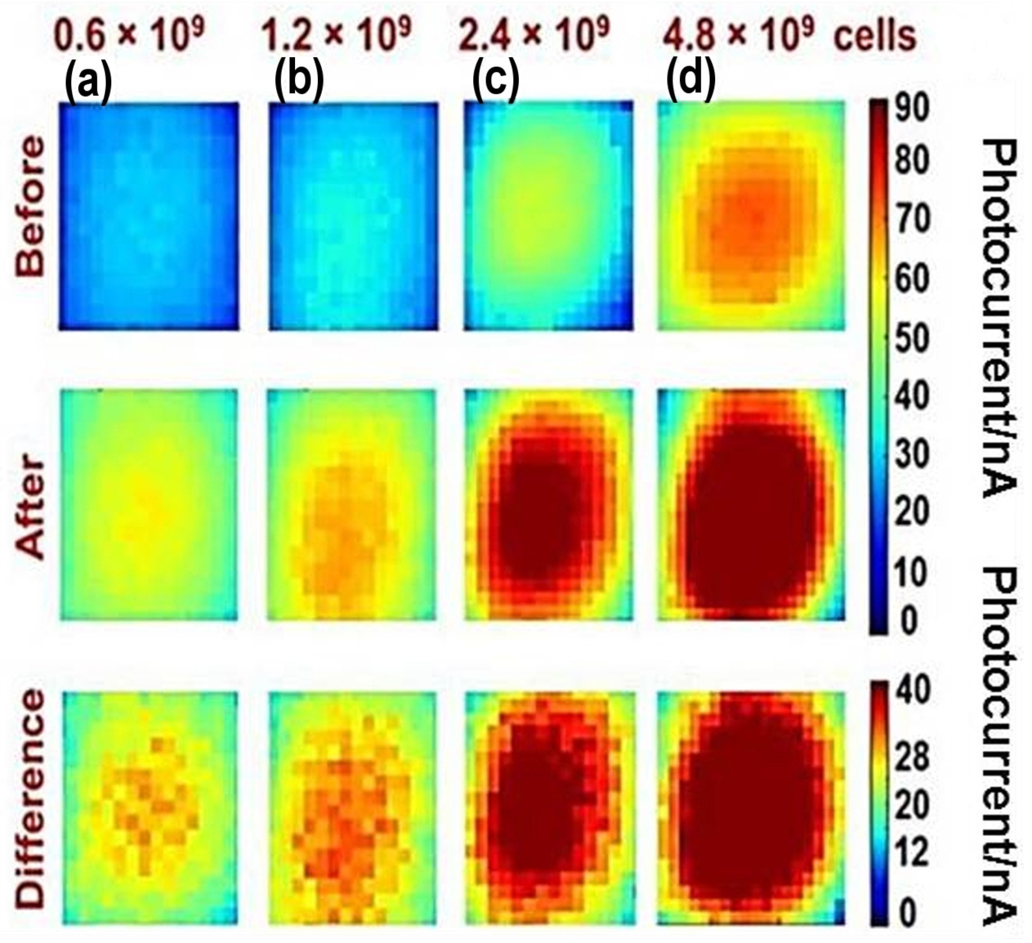
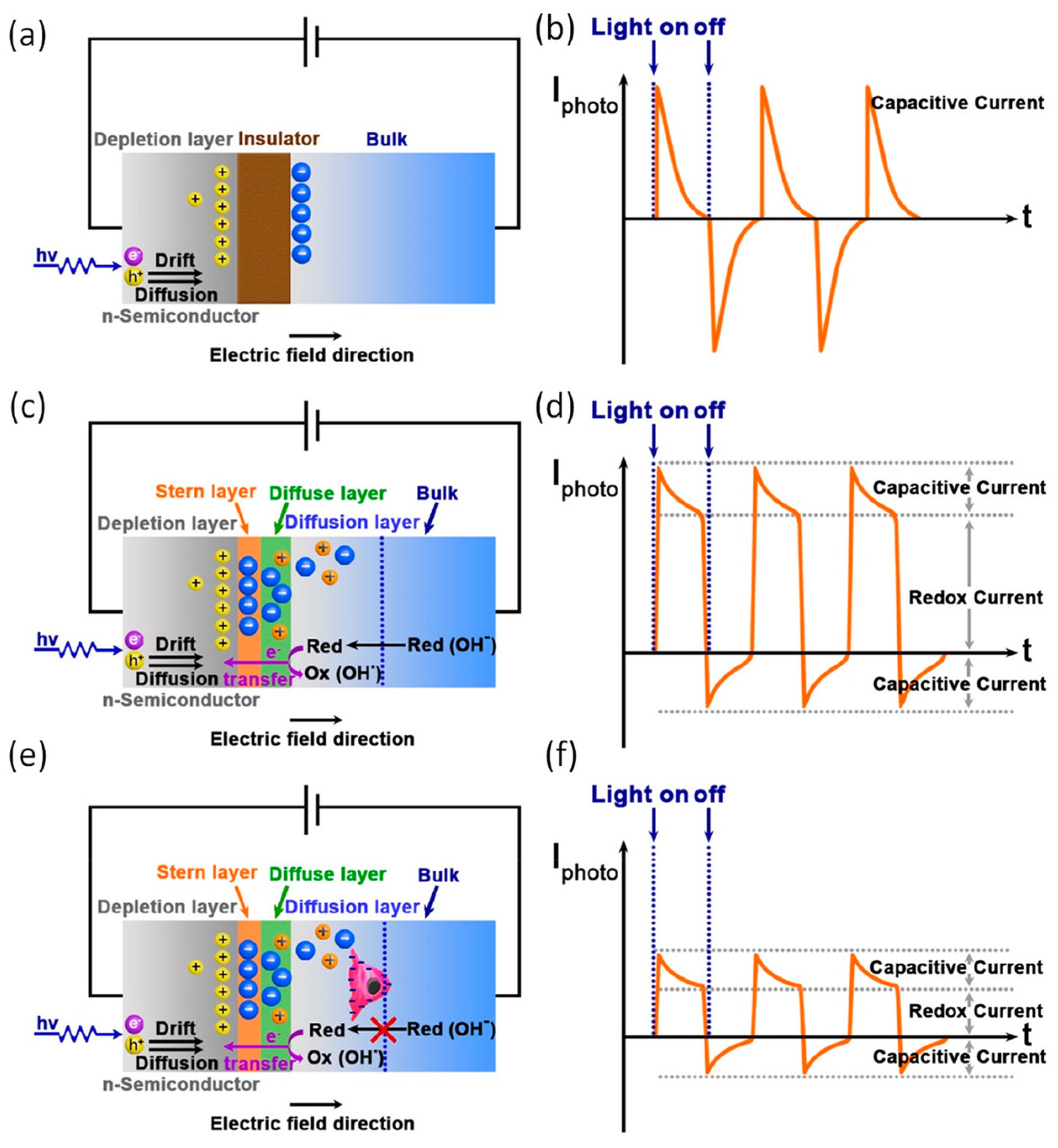
5. From Equilibrium to Non-Equilibrium Systems

Although the output signal of a LAPS is the amplitude of an alternating current, Isig, as measured by an ammeter, a LAPS is a potentiometric sensor because no direct current flows through its EIS structure as the direct current is blocked by the insulator layer. Therefore, a LAPS measurement is not associated with any electrochemical reaction, and the system stays at equilibrium. On one hand, the absence of a direct current guarantees that it is a non-destructive method, meaning that the solution under test is not affected by the measurement. On the other hand, being a potentiometric method can also be a limitation, especially in its application to biosensing based on amperometric principles.
A straightforward way of combining an electrochemical system and a LAPS measurement is illustrated in Figure 10, where an electrochemical reaction takes place on the working electrode (WE) under polarization in a three-electrode system, and a LAPS attached as an additional electrode monitors the reaction. This configuration was used in the study of a corroding surface [37], in which the pH change in the vicinity of this corroding surface under polarization was monitored by a LAPS, as shown in Figure 5.
In the configuration in Figure 10, the measurement on the LAPS surface is light-addressable, but the position on the WE surface where the electrochemical reaction takes place is not addressable. There are several approaches to specify the location of an electrochemical reaction. Well-known examples include the mechanical scanning by an ultramicroelectrode (UME) in scanning electrochemical microscopy (SECM) [42] and the individual access to one of the electrodes in a microelectrode array (MEA) [43,44] used in neurophysiology. Inoue et al. [45] developed a large-scale integrated circuit device called Bio-LSI, which consisted of 400 microelectrodes with peripheral circuits and functioned as an array of amperometric sensors that could visualize electrochemical reactions.
As an alternative to an MEA, a light-addressable electrode (LAE) [15,46] was developed and was mainly aimed at stimulating and probing cultured neurons in a spatially resolved manner. Compared with an MEA, in which the size of electrodes and their positions are pre-defined, an arbitrary area on the LAE surface can be activated by illumination. The basic concept of such a system can be found, for example, in the patent application filed in 1995 by Sugihara et al. [47], but various implementations have been proposed to date. In most LAEs, photocarriers are excited by illuminating a semiconductor layer, and an electrical pathway is created to access the particular neuron on the surface. Bucher et al. [16] inserted an underlying a-Si:H layer beneath an MEA and utilized the photoconductivity of a-Si:H to select individual electrodes in the array. Colicos et al. [17] cultured neurons on a Si surface, and only the neuronal cell body of interest was illuminated under the microscope to enhance the conductivity of Si directly under the selected neuron. An electrical pulse was then exclusively applied to the selected neuron through the region of enhanced conductivity, which functioned as a virtual probe. Starovoytov et al. [18] also cultured neurons on a Si surface, and extracellular stimulation was realized by generating an electrical current near the neuron via a pulsed illumination under a constant bias condition. Suzurikawa et al. [15] cultured neurons on a layered structure, as shown in Figure 11, which consisted of a passivation layer of zinc antimonate sol and bisphenol-F epoxy resin, a photoconductive layer of a-Si:H, and a conductive layer of SnO2 deposited on a glass substrate. Neurons were cultured on the passivation layer, and a highly conductive region in the a-Si:H layer, defined by illumination, was employed as a virtual probe to electrically stimulate the neurons only inside the illuminated region.
Whereas many LAEs have been mainly targeted at spatially resolved interrogation of neurons, Choudhury et al. [22] proposed a more versatile method that has potential applications in a wide range of electrochemistry. This method, which was named light-activated electrochemistry (also abbreviated as LAE) [48,49,50], allows a direct current to flow from the Si electrode into the solution only at the illuminated site and thereby activates localized faradaic electrochemistry on the surface. As shown in Figure 12a, a monolayer of 1,8-nonadiyne (to prevent oxidation) is formed on the Si surface, and a redox mediator (ferrocene) is attached to the distal end. A bias voltage is applied between the solution and the Si to form a SCL at the Si surface, where the internal electric field separates electrons and holes generated by illumination, as shown in Figure 12b. When holes gather at the surface, electron transfer from ferrocene to Si is possible [51], allowing a localized direct current to flow. The size of the active site on the surface can be reduced by using a focused light beam so that it can function like a UME in SECM. Light-activated electrochemistry has been applied to two-dimensional interrogation (“electrochemical reading”) [48,50] as well as electrochemical deposition on the surface (“electrochemical writing”) [50]. When combined with an amperometric sensing principle, it can potentially be applied to a device that should be called a light-addressable amperometric sensor (LAAS) [20,21,52,53,54,55] or a light-addressable electrochemical sensor (LAE sensor) [8,56,57,58,59].
Wu et al. [23] proposed yet another modality, the photoelectrochemical imaging system (PEIS), which is a hybrid of light-activated electrochemistry and LAPS [60]. An ITO-coated glass was used as a substrate, which allowed electron transfer from the solution to the ITO under illumination without the help of a redox mediator. A direct current flows, therefore, at the illuminated site in a way comparable to that in light-activated electrochemistry, and in addition, the illumination is modulated in a way similar to that in a LAPS, resulting in a transient current. Figure 13a,b shows the layer structure of the LAPS and the waveform of the signal current. As the surface is insulated, no direct current flows, and only a transient current charging and discharging the capacitance (capacitive current) flows when the light is switched on and off. Figure 13c illustrates the layer structure of a PEIS, where the semiconductor ITO is in contact with the solution without insulation. As displayed in Figure 13d, a direct current (redox current) flows while the light is on, and in addition, a transient current (capacitive current) flows when the light is switched on and off. They found that the redox current was sensitive to the negative surface charges of a cell in the vicinity of the surface, as shown in Figure 13e,f. They successfully applied this imaging modality to visualize the distribution of surface charges on the basal side of a single living cell cultured on the surface [23].
Furthermore, Zhou et al. [61] improved the performance of a PEIS by replacing ITO with α-Fe2O3 (hematite) and employing analog micromirrors for high-speed scanning. The experiment enabled visualization of the permeabilization process of cellular membranes by a surfactant, i.e., Triton X-100, at a temporal resolution of eight frames per second. They also applied hematite nanorods for photoelectrochemical sensing of calcium ions [62]. Welden et al. [63] reported on the dependence of the photogenerated faradaic current on pH when a layer structure of glass/SnO2:F/TiO2/solution was periodically illuminated. The pH sensitivity of the faradaic current was applied to detect the pH change due to an enzymatic reaction catalyzed by penicillinase and to determine the penicillin concentration.

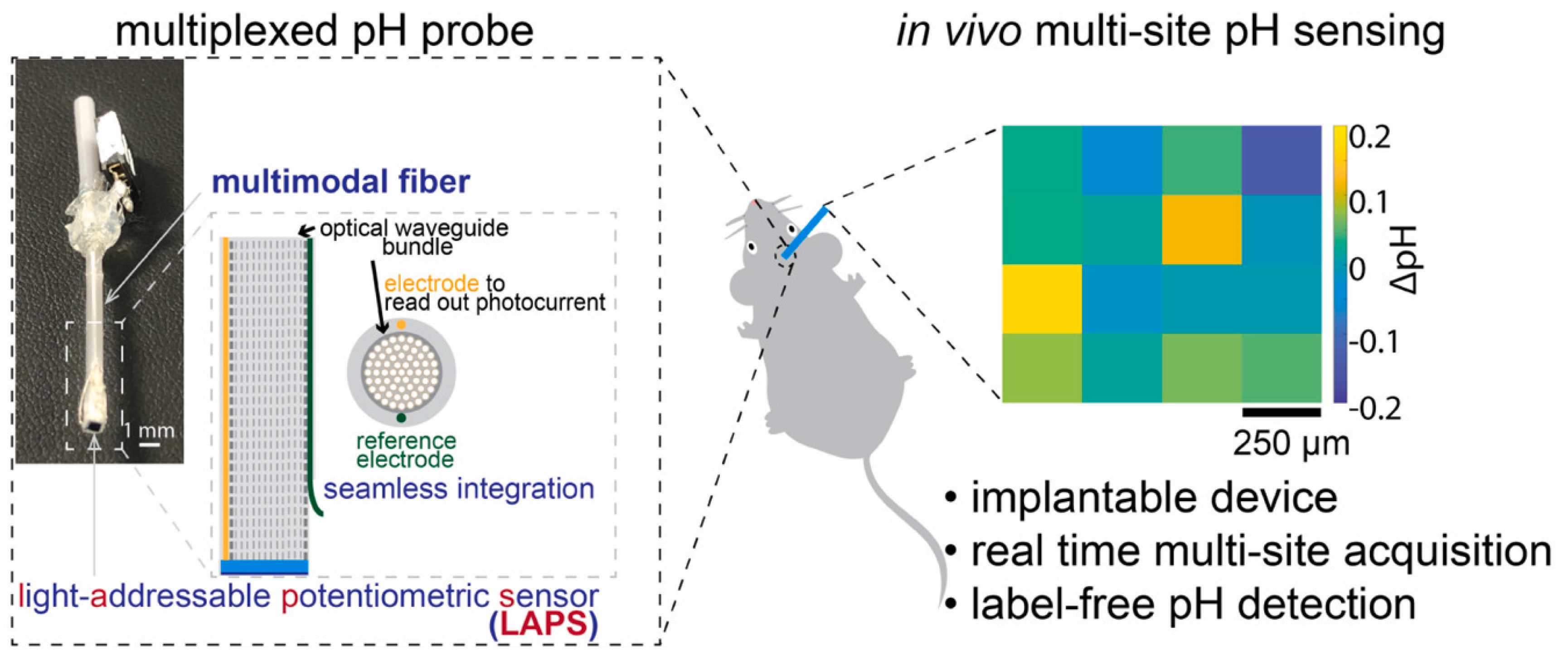
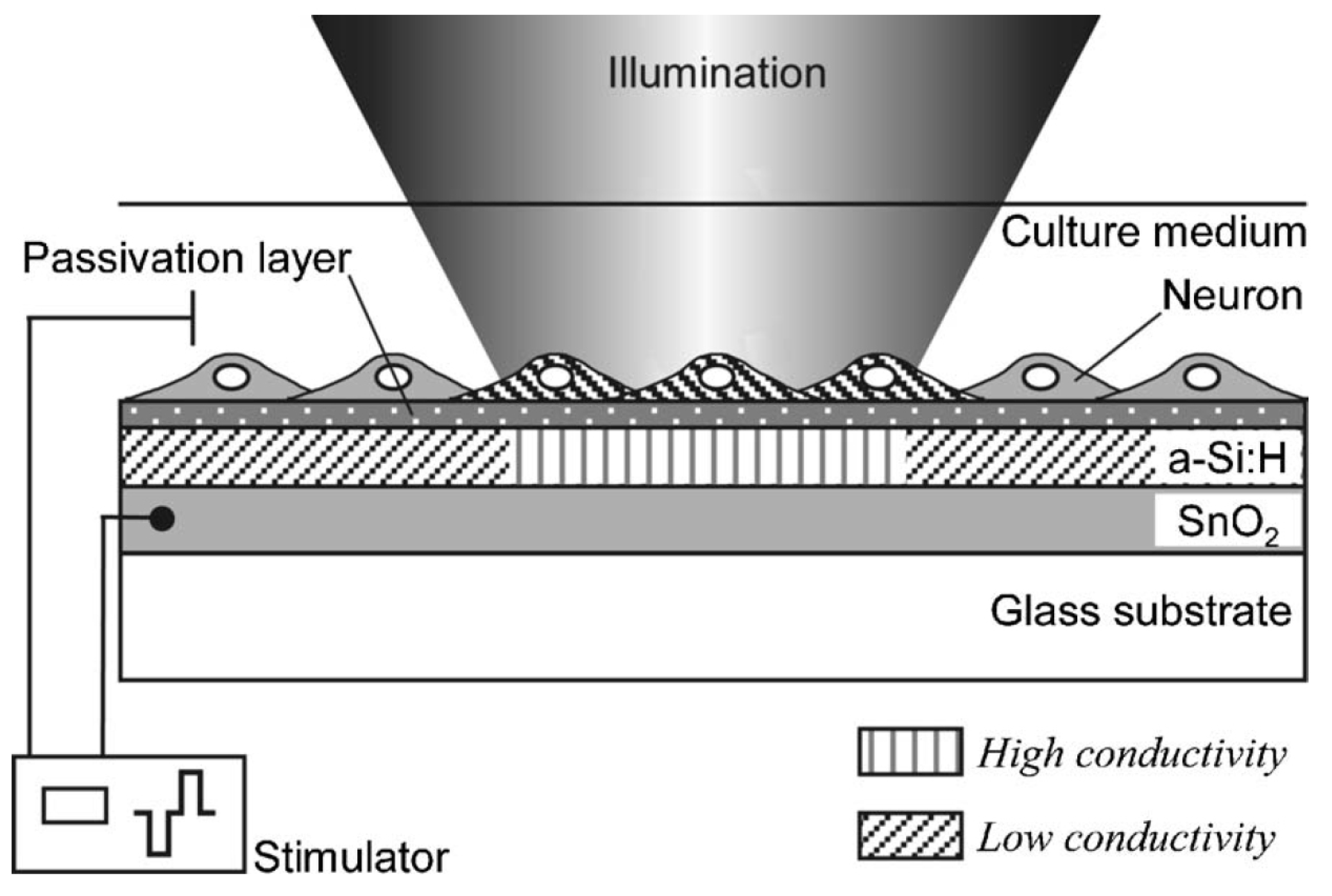
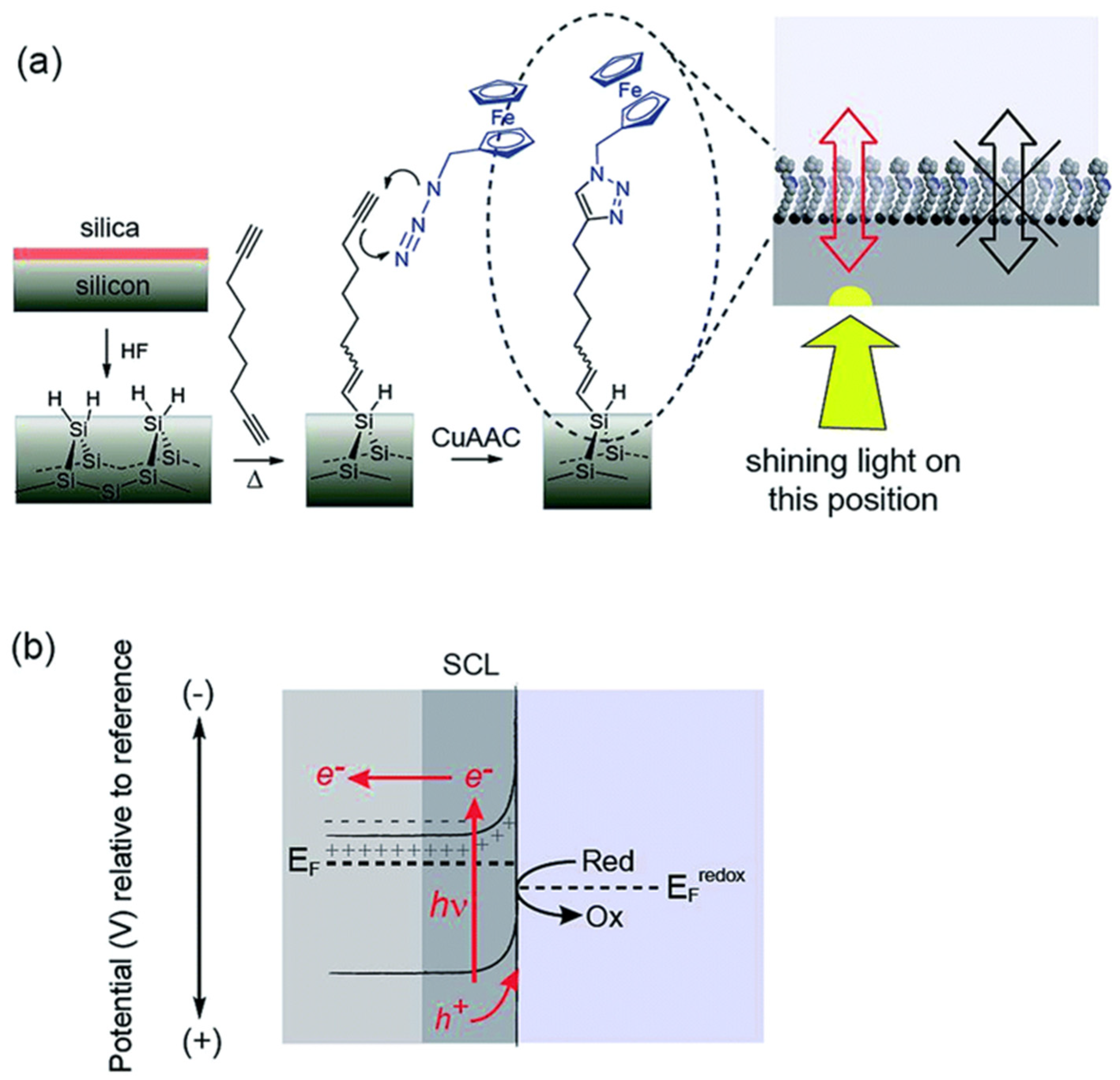
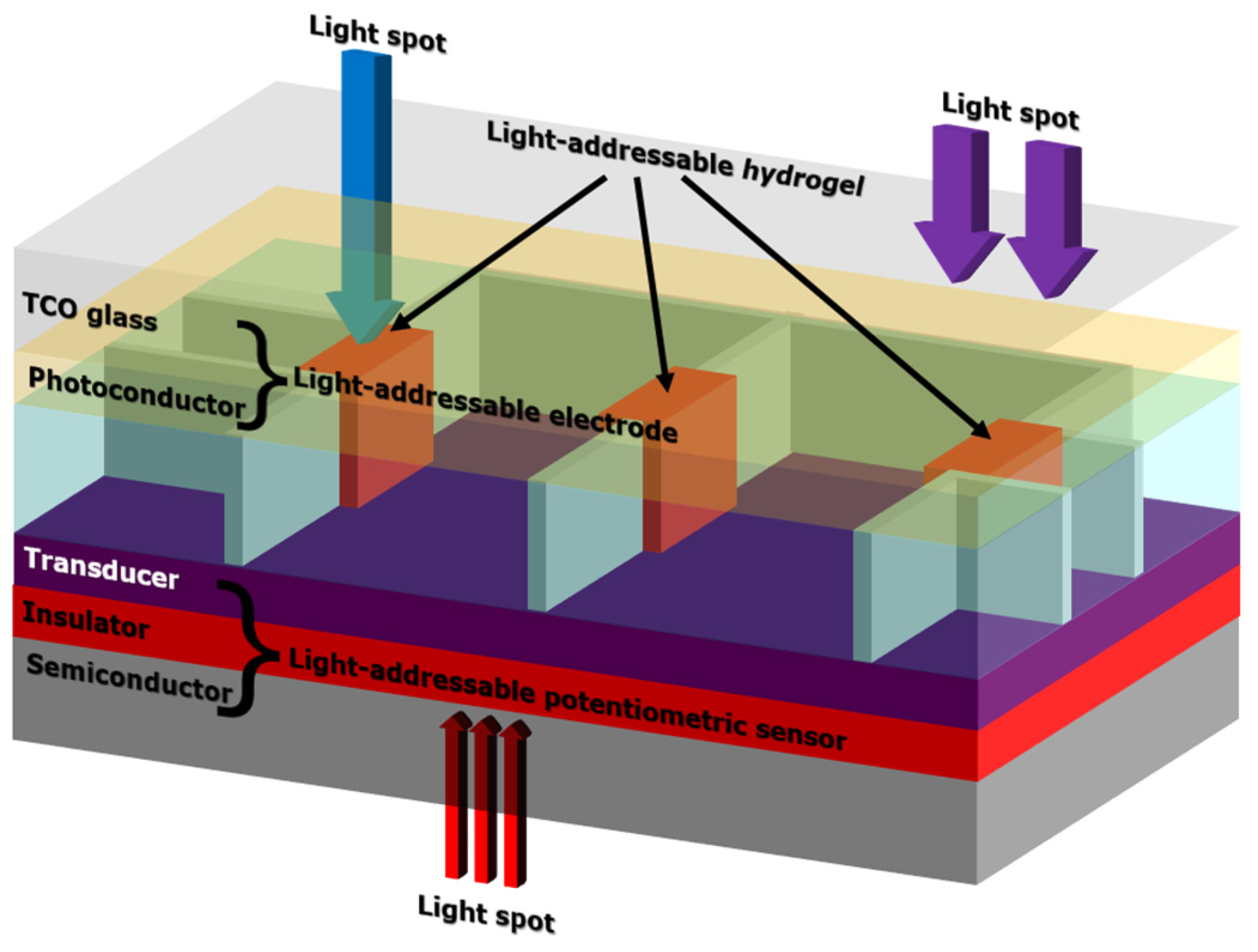
6. Combination of Light-Addressing Technologies and Light-Addressed Actuation

A careful choice of a suitable light source, including the spatial dimensions and profile of the light beam, its wavelength, as well as the modulation of light intensity, is crucial for the design of SLPT and LAPS systems. Furthermore, these technologies ensure the unhindered access of the light beam to the sensor plate. To meet these demands, the design and placement of the light system, sophisticated beam guiding, and the use of transparent materials are key factors. The light source systems wield the potential for synergistic alliances with related technologies reliant on similar light sources. The obstacle might be the seamless integration of diverse spectroscopy methods. Even when not tethered to identical light sources, the presence of optical windows and waveguides within SLPT or LAPS configurations enables a rather effortless combination [64].
Recently, LAPS systems have found their niche in microfluidic setups, addressing the needs of lab-on-a-chip or micro-total-analysis systems [65,66,67,68]. A common concept in these systems is the combination of sensors and actuator functionalities within a spatially confined space. Leveraging light to activate actuators for manipulating liquid flows or altering liquid properties is emerging as a promising method to reduce system complexity and costs. As described in the previous section, one promising application in combination with LAPS involves the deployment of LAEs. Owing to the limited liquid volumes within microfluidic channels, the utilization of LAE allows the chemical modification of liquid properties. Consequently, this facilitates precise control over chemical reactions within specified regions on a lab-on-a-chip system. Illuminating a defined area renders it highly conductive, while non-illuminated regions remain nearly non-conductive. Applying a bias voltage empowers users to address specific locations on an actuator plate where high direct currents can flow. These direct currents find diverse applications, e.g., for water splitting to locally alternating the pH value within a microfluidic channel [69,70].
A second approach relies on harnessing a light beam as an energy source to locally induce heat in a lab-on-a-chip system. This necessitates the use of materials boasting a high photon absorption coefficient. The resulting localized thermal gradients within microfluidic channels can be utilized for multiple purposes. An exemplary application was reported in tandem with thermo-sensitive hydrogels, which undergo distinct states below and above the lower critical solution temperature. The incorporation of graphene oxide into these hydrogels allows precise control of their states using the modified light source of a LAPS system. It was demonstrated recently that this enables the design of microfluidic devices in which valve functions controlled by a light beam and a LAPS setups for electrochemical readouts are embedded [71]. Figure 14 shows a schematic which depicts the integration of a LAPS, a LAE, and a light-addressable hydrogel to establish a lab-on-a-chip system controlled by light.
Numerous light-assisted technologies which are reported in the literature can be potentially combined with the SLPT or LAPS technique. Synergies with technologies, like optogenetics [72], photonic crystals [73,74], or further methods to control microfluidic setups [75,76] hold promise for further miniaturizing and simplifying lab-on-a-chip setups as well as contributing to novel applications in the future.

7. Summary

The artificial olfactory image was proposed by Lundström et al. in 1991 as a new approach to realize an electronic nose system. In this approach, for the first time, a photocurrent image was introduced as a fingerprint of the gas by applying the SLPT to an MOS structure with catalytic metal gates such as Pt, Ir, and Pd. Whereas the preceding research on the SLPT mainly focused on interrogation of the MOS structure itself, the artificial olfactory image (for gases) and the LAPS (for ions) successfully demonstrated the possibility of applying the SLPT to chemical sensors. From a historical point of view, in the following decades, this essentially stimulated scientists from different fields and drove the development of various modalities of chemical imaging sensors based on light-addressed field-effect structures. The target analytes investigated so far include not only gases, pH, and different cations and anions (e.g., Na+, K+, Li+, Ca2+, Mg2+, Cd2+, Pb2+, Cl, NO3, and SO42−) with the help of ion-selective membranes, but also various reactions of enzymes with their counteracting substrate molecules. (The enzymes utilized include penicillinase, urease, glucose oxidase, alcohol dehydrogenase, and cholinesterase.) In addition, the detection of charged macromolecules such as DNA has received considerable interest, as well as the study of the metabolic activity of living organisms (e.g., E. coli, L. brevis, Chinese hamster ovary cells, and cancer cells), with the help of biosensing principles combined with the field-effect structure. The progress in light scanning technology and data processing has realized a high spatial resolution down to the submicrometer range and a high video frame rate of up to 200 fps. Recently, light-addressing technology was further employed in position-specified activation of the electrode surface in light-addressable electrodes and light-activated chemistry, as well as for the actuation of liquids in microfluidic devices. As presented in the literature, the incorporation of light-activated hydrogel valves in microfluidic channels demonstrates that light can serve for chemical sensing and modification, and also facilitate physical interactions, such as the control of flow directions and speed.
The most essential feature that the light-addressing technologies share is that they can define an arbitrary size and shape of active area on a sensing surface or on an electrode surface; only the locally illuminated area serves as a sensing surface for potentiometry or amperometry, or as an electrode for electrochemistry and neural stimulation. The surface of a single chip can be divided into a huge number of virtual sensors or electrodes, which can be sequentially addressed by a scanning light beam so that they are functionally equivalent to a huge array of discrete sensors or electrodes. In contrast to a physical array of sensors or electrodes, the light-addressing technology offers the following merits: First, the layout of pixels can be flexibly changed at the time of use. This attribute can be exploited to realize a zoom-in function by changing the field of view and the magnification. Second, wiring to individual pixels is not required [22], which offers a great benefit in terms of the fabrication cost as well as the reliability of the device. On the other hand, one drawback might be a lower temporal resolution, which is inherent to a scanning method.
Studies on the development and improvement of light-addressing technologies as well as their applications are accelerating fast and have extended into diverse directions in recent years. Various materials, such as InGaN [77], SnOx [78], indium gallium zinc oxide (IGZO) [79,80], fullerene (C60) [81], layer-by-layer assembly of carbon dots and liquid exfoliated graphene [82], benzodithiophene-based polymer PTB7-Th/fullerene PC71BM [83], and nitrogen-doped graphene quantum dots [84], have been tested as a photosensitive active layer to replace silicon, as well as fluorographene [85] as a sensing membrane. Optimization of the sensor structure has also been studied to obtain a higher spatial resolution [86,87,88,89,90]. As for the applications, many studies are directed to biosensing applications, including the detection of DNA hybridization [56,91], determination of glucose [92,93] and okadaic acid [94], as well as immunoassays of antigens [95]. Many studies are especially oriented to the detection of clinical biomarkers such as circulating tumor cells [96], alpha-fetoprotein [97], 1,5-anhydroglucitol [98], glypican-3 [99], and low-density lipoprotein [100]. The light-addressing technologies are also applied to cells, including the detection of extracellular acidification due to metabolism [67,101], light absorption of live cells [102], action potentials of cardiomyocytes [103], and apoptosis [104]. Finally, new measurement modalities have also been explored, including the combination of square-wave voltammetry and light-addressing technology [105], as well as the use of a scanning electron beam instead of a light beam for excitation of carriers in a semiconductor [106,107].

Author Contributions

Conceptualization, T.Y. and M.J.S.; writing—original draft preparation, T.Y., M.J.S. and T.W.; writing—review and editing, T.Y., K.-i.M., T.W. and M.J.S. All authors have read and agreed to the published version of the manuscript.

Funding

This research received no external funding.

Conflicts of Interest

The authors declare no conflicts of interest.

References

  1. Lundström, I.; Erlandsson, R.; Frykman, U.; Hedborg, E.; Spetz, A.; Sundgren, H.; Welin, S.; Winquist, F. Artificial ‘olfactory’ images from a chemical sensor using a light pulse technique. Nature 1991, 352, 47–50. [Google Scholar] [CrossRef]
  2. Winquist, F.; Sundgren, H.; Hedborg, E.; Spetz, A.; Lundström, I. Visual images of gas mixtures produced with field-effect structures. Sens. Actuators B 1992, 6, 157–161. [Google Scholar] [CrossRef]
  3. Lundström, I.; Svensson, C.; Spetz, A.; Sundgren, H.; Winquist, F. From hydrogen sensors to olfactory images—Twenty years with catalytic field-effect devices. Sens. Actuators B 1993, 13, 16–23. [Google Scholar] [CrossRef]
  4. Engström, O.; Carlsson, A. Scanned light pulse technique for the investigation of insulator–semiconductor interfaces. J. Appl. Phys. 1983, 54, 5245–5251. [Google Scholar] [CrossRef]
  5. Hafeman, D.G.; Parce, J.W.; McConnell, H.M. Light-addressable potentiometric sensor for biochemical systems. Science 1988, 240, 1182–1185. [Google Scholar] [CrossRef] [PubMed]
  6. Yoshinobu, T.; Miyamoto, K.; Werner, C.F.; Poghossian, A.; Wagner, T.; Schöning, M.J. Light-addressable potentiometric sensors for quantitative spatial imaging of chemical species. Annu. Rev. Anal. Chem. 2017, 10, 225–246. [Google Scholar] [CrossRef] [PubMed]
  7. Liu, Y.; Zhu, P.; Liu, S.; Chen, Y.; Liang, D.; Wang, M.; Du, L.; Wu, C. The Light-addressable potentiometric sensor and its application in biomedicine towards chemical and biological sensing. Chemosensors 2022, 10, 156. [Google Scholar] [CrossRef]
  8. Meng, Y.; Chen, F.; Wu, C.; Krause, S.; Wang, J.; Zhang, D.-W. Light-addressable electrochemical sensors toward spatially resolved biosensing and imaging applications. ACS Sens. 2022, 7, 1791–1807. [Google Scholar] [CrossRef]
  9. Luo, J.; Liu, S.; Chen, Y.; Tan, J.; Zhao, W.; Zhang, Y.; Li, G.; Du, Y.; Zheng, Y.; Li, X.; et al. Light addressable potentiometric sensors for biochemical imaging on microscale: A review on optimization of imaging speed and spatial resolution. ACS Omega 2023, 8, 42028–42044. [Google Scholar] [CrossRef]
  10. Ito, Y.; Morimoto, K.; Tsunoda, Y. Light-addressable potentiometric (LAP) gas sensor. Sens. Actuators B 1993, 13, 348–350. [Google Scholar] [CrossRef]
  11. Pecora, A.; Fortunato, G.; Carluccio, R.; Sacco, S. Hydrogenated amorphous silicon based light-addressable potentiometric sensor (LAPS) for hydrogen detection. J. Non-Cryst. 1993, 164–166, 793–796. [Google Scholar] [CrossRef]
  12. Kanai, Y.; Shimizu, M.; Uchida, H.; Nakahara, H.; Zhou, C.G.; Maekawa, H.; Katsube, T. Integrated taste sensor using surface photovoltage technique. Sens. Actuators B 1994, 20, 175–179. [Google Scholar] [CrossRef]
  13. Shimizu, M.; Kanai, Y.; Uchida, H.; Katsube, T. Integrated biosensor employing a surface photovoltage technique. Sens. Actuators B 1994, 20, 187–192. [Google Scholar] [CrossRef]
  14. Nakao, M.; Yoshinobu, T.; Iwasaki, H. Scanning-laser-beam semiconductor pH-imaging sensor. Sens. Actuators B 1994, 20, 119–123. [Google Scholar] [CrossRef]
  15. Suzurikawa, J.; Takahashi, H.; Kanzaki, R.; Nakao, M.; Takayama, Y.; Jimbo, Y. Light-addressable electrode with hydrogenated amorphous silicon and low-conductive passivation layer for stimulation of cultured neurons. Appl. Phys. Lett. 2007, 90, 093901. [Google Scholar] [CrossRef]
  16. Bucher, V.; Brunner, B.; Leibrock, C.; Schubert, M.; Nisch, W. Electrical properties of a light-addressable microelectrode chip with high electrode density for extracellular stimulation and recording of excitable cells. Biosens. Bioelectron. 2001, 16, 205–210. [Google Scholar] [CrossRef]
  17. Colicos, M.A.; Collins, B.E.; Sailor, M.J.; Goda, Y. Remodeling of synaptic actin induced by photoconductive stimulation. Cell 2001, 107, 605–616. [Google Scholar] [CrossRef] [PubMed]
  18. Starovoytov, A.; Choi, J.; Seung, H.S. Light-directed electrical stimulation of neurons cultured on silicon wafers. J. Neurophysiol. 2005, 93, 1090–1098. [Google Scholar] [CrossRef] [PubMed]
  19. Krause, S.; Talabani, H.; Xu, M.; Moritz, W.; Griffiths, J. Scanning photo-induced impedance microscopy—An impedance based imaging technique. Electrochim. Acta 2002, 47, 2143–2148. [Google Scholar] [CrossRef]
  20. Hagiwara, T.; Takazawa, M.; Uchida, H.; Hasegawa, Y.; Yaji, T. An amperometric sensor for chemical imaging using photoconductive organic film. IEICE Trans. Electron. 2008, E91.C, 1863–1868. [Google Scholar] [CrossRef]
  21. Arai, H.; Goto, D.; Hasegawa, Y.; Uchida, H. Study on the two-dimensional chemical sensor using a photoconductive polymer film. IEEJ Trans. Sens. Micromachines 2013, 133, 290–296. [Google Scholar] [CrossRef]
  22. Choudhury, M.H.; Ciampi, S.; Yang, Y.; Tavallaie, R.; Zhu, Y.; Zarei, L.; Gonçalesa, V.R.; Gooding, J.J. Connecting electrodes with light: One wire, many electrodes. Chem. Sci. 2015, 6, 6769–6776. [Google Scholar] [CrossRef]
  23. Wu, F.; Zhou, B.; Wang, J.; Zhong, M.; Das, A.; Watkinson, M.; Hing, K.; Zhang, D.W.; Krause, S. Photoelectrochemical imaging system for the mapping of cell surface charges. Anal. Chem. 2019, 91, 5896–5903. [Google Scholar] [CrossRef]
  24. Bergveld, P. Development of an ion-sensitive solid-state device for neurophysiological measurements. IEEE Trans. Biomed. Eng. 1970, 17, 70–71. [Google Scholar] [CrossRef] [PubMed]
  25. Wagner, T.; Schöning, M.J. Light-addressable potentiometric sensors (LAPS): Recent trends and applications. In Electrochemical Sensor Analysis; Alegret, S., Merkoçi, A., Eds.; Elsevier: Amsterdam, The Netherlands, 2007; pp. 87–128. [Google Scholar]
  26. Liang, T.; Qiu, Y.; Gan, Y.; Sun, J.; Zhou, S.; Wan, H.; Wang, P. Recent developments of high-resolution chemical imaging systems based on light-addressable potentiometric sensors (LAPSs). Sensors 2019, 19, 4294. [Google Scholar] [CrossRef] [PubMed]
  27. Yoshinobu, T.; Schöning, M.J. Light-addressable potentiometric sensors for cell monitoring and biosensing. Curr. Opin. Electrochem. 2021, 28, 100727. [Google Scholar] [CrossRef]
  28. Lundström, I.; Shivaraman, M.S.; Svensson, C.M. A hydrogen-sensitive Pd-gate MOS transistor. J. Appl. Phys. 1975, 6, 3876–3881. [Google Scholar] [CrossRef]
  29. Sundgren, H.; Lundström, I.; Winquist, F.; Lukkari, I.; Carlsson, R.; Wold, S. Evaluation of multiple gas mixture with a simple MOSFET gas sensor array and pattern recognition. Sens. Actuators B 1990, 2, 115–123. [Google Scholar] [CrossRef]
  30. Sato, T.; Shimizu, M.; Uchida, H.; Katsube, T. Light-addressable suspended-gate gas sensor. Sens. Actuators B 1994, 20, 213–216. [Google Scholar] [CrossRef]
  31. Yamada, T.; Zhou, H.S.; Uchida, H.; Tomita, M.; Ueno, Y.; Honma, I.; Asai, K.; Katsube, T. Application of a cubic-like mesoporous silica film to a surface photovoltage gas sensing system. Microporous Mesoporous Mater. 2002, 54, 269–276. [Google Scholar] [CrossRef]
  32. Zhang, Q.; Wang, P.; Li, J.; Gao, X. Diagnosis of diabetes by image detection of breath using gas-sensitive LAPS. Biosens. Bioelectron. 2000, 15, 249–256. [Google Scholar] [CrossRef]
  33. Ermolenko, Y.; Yoshinobu, T.; Mourzina, Y.; Levichev, S.; Furuichi, K.; Vlasov, Y.; Schöning, M.J.; Iwasaki, H. Photocurable membranes for ion-selective light-addressable potentiometric sensor. Sens. Actuators B 2002, 85, 79–85. [Google Scholar] [CrossRef]
  34. Wu, Y.; Wang, P.; Ye, X.; Zhang, Q.; Li, R.; Yan, W.; Zheng, X. A novel microphysiometer based on MLAPS for drugs screening. Biosens. Bioelectron. 2001, 16, 277–286. [Google Scholar] [CrossRef]
  35. Bousse, L.; McReynolds, R.J.; Kirk, G.; Dawes, T.; Lam, P.; Bemiss, W.R.; Parce, J.W. Micromachined multichannel systems for the measurement of cellular metabolism. Sens. Actuators B 1994, 20, 145–150. [Google Scholar] [CrossRef]
  36. Nakao, M.; Inoue, S.; Oishi, R.; Yoshinobu, T.; Iwasaki, H. Observation of microorganism colonies using a scanning-laser-beam pH-sensing microscope. J. Ferment. Bioeng. 1995, 79, 163–166. [Google Scholar] [CrossRef]
  37. Miyamoto, K.; Sakakita, S.; Wagner, T.; Schöning, M.J.; Yoshinobu, T. Application of chemical imaging sensor to in-situ pH imaging in the vicinity of a corroding metal surface. Electrochim. Acta 2015, 183, 137–142. [Google Scholar] [CrossRef]
  38. Dantism, S.; Takenaga, S.; Wagner, T.; Wagner, P.; Schöning, M.J. Differential imaging of the metabolism of bacteria and eukaryotic cells based on light-addressable potentiometric sensors. Electrochim. Acta 2017, 246, 234–241. [Google Scholar] [CrossRef]
  39. Guo, Y.; Werner, C.F.; Handa, S.; Wang, M.; Ohshiro, T.; Mushiake, H.; Yoshinobu, T. Miniature multiplexed label-free pH probe in vivo. Biosens. Bioelectron. 2021, 174, 112870. [Google Scholar] [CrossRef] [PubMed]
  40. Wu, F.; Campos, I.; Zhang, D.W.; Krause, S. Biological imaging using light-addressable potentiometric sensors and scanning photo-induced impedance microscopy. Proc. R. Soc. A 2017, 473, 20170130. [Google Scholar] [CrossRef] [PubMed]
  41. Chen, L.; Zhou, Y.; Jiang, S.; Kunze, J.; Schmuki, P.; Krause, S. High resolution LAPS and SPIM. Electrochem. Commun. 2010, 12, 758–760. [Google Scholar] [CrossRef]
  42. Bard, A.J.; Fan, F.R.K.; Kwak, J.; Lev, O. Scanning electrochemical microscopy. Introduction and principles. Anal. Chem. 1989, 61, 132–138. [Google Scholar] [CrossRef]
  43. Thomas, C.A., Jr.; Springer, P.A.; Loeb, G.E.; Berwald-Netter, Y.; Okun, L.M. A miniature microelectrode array to monitor the bioelectric activity of cultured cells. Exp. Cell Res. 1972, 74, 61–66. [Google Scholar] [CrossRef] [PubMed]
  44. Spira, M.E.; Hai, A. Multi-electrode array technologies for neuroscience and cardiology. Nat. Nanotechnol. 2013, 8, 83–94. [Google Scholar] [CrossRef] [PubMed]
  45. Inoue, K.Y.; Matsudaira, M.; Kubo, R.; Nakano, M.; Yoshida, S.; Matsuzaki, S.; Suda, A.; Kunikata, R.; Kimura, T.; Tsurumi, R.; et al. LSI-based amperometric sensor for bio-imaging and multi-point biosensing. Lab Chip 2012, 12, 3481–3490. [Google Scholar] [CrossRef] [PubMed]
  46. Welden, R.; Schöning, M.J.; Wagner, P.H.; Wagner, T. Light-addressable electrodes for dynamic and flexible addressing of biological systems and electrochemical reactions. Sensors 2020, 20, 1680. [Google Scholar] [CrossRef] [PubMed]
  47. Sugihara, H.; Taketani, M.; Kamei, A.; Iwasaki, H. Two-Dimensional Sensor for Measuring Nerve Cell Activity and Measurement Device Using It. Japanese Patent 2,930,182, 3 August 1999. [Google Scholar]
  48. Yang, Y.; Ciampi, S.; Zhu, Y.; Gooding, J.J. Light-activated electrochemistry for the two-dimensional interrogation of electroactive regions on a monolithic surface with dramatically improved spatial resolution. J. Phys. Chem. C 2016, 120, 13032–13038. [Google Scholar] [CrossRef]
  49. Kashi, M.B.; Silva, S.M.; Yang, Y.; Gonçales, V.R.; Parker, S.G.; Barfidokht, A.; Ciampi, S.; Gooding, J.J. Light-activated electrochemistry without surface-bound redox species. Electrochim. Acta 2017, 251, 250–255. [Google Scholar] [CrossRef]
  50. Vogel, Y.B.; Gonçales, V.R.; Gooding, J.J.; Ciampi, S. Electrochemical microscopy based on spatial light modulators: A projection system to spatially address electrochemical reactions at semiconductors. J. Electrochem. Soc. 2018, 165, H3085–H3092. [Google Scholar] [CrossRef]
  51. Gerischer, H. Electrochemical behavior of semiconductors under illumination. J. Electrochem. Soc. 1966, 113, 1174–1182. [Google Scholar] [CrossRef]
  52. Shichijo, M.; Hasegawa, Y.; Uchida, H. Study of detection method for collagenase enzyme reaction using two dimensional electrochemical sensor. Electron. Commun. Jpn. 2020, 103, 90–96. [Google Scholar] [CrossRef]
  53. Kosugi, K.; Uchida, H. Study of LAAS sensitivity using back surface electric field. IEEJ Trans. Sens. Micromachines 2021, 141, 14–20. [Google Scholar] [CrossRef]
  54. Kosugi, K.; Hasegawa, Y.; Uchida, H. Light-addressable amperometric sensor with counter and working electrodes of the same material. IEEJ Trans. Electr. Electron. Eng. 2021, 16, 478–485. [Google Scholar] [CrossRef]
  55. Miyairi, A.; Hasegawa, Y.; Uchida, H. Measurement of acetylcholinesterase using a two-dimensional electrochemical sensor LAAS. Electron. Commun. Jpn. 2023, 106, e12425. [Google Scholar] [CrossRef]
  56. Zarei, L.; Tavallaie, R.; Choudhury, M.H.; Parker, S.G.; Bakthavathsalam, P.; Ciampi, S.; Gonçales, V.R.; Gooding, J.J. DNA hybridization detection on Si(100) surfaces using light-activated electrochemistry: A comparative study between bovine serum albumin and hexaethylene glycol as antifouling layers. Langmuir 2018, 34, 14817–14824. [Google Scholar] [CrossRef] [PubMed]
  57. Terrero Rodríguez, I.M.; Borrill, A.J.; Schaffer, K.J.; Hernandez, J.B.; O’Neil, G.D. Light-addressable electrochemical sensing with electrodeposited n-silicon/gold nanoparticle Schottky junctions. Anal. Chem. 2020, 92, 11444–11452. [Google Scholar] [CrossRef] [PubMed]
  58. Hernandez, J.B.; Epright, Z.D.; Terrero Rodríguez, I.M.; O’Neil, G.D. Electrodeposition parameters dramatically influence the morphology, stability, and performance of n-Si/Pt light-addressable electrochemical sensors. ChemElectroChem 2023, 10, e202300400. [Google Scholar] [CrossRef]
  59. Arthur, E.G.; Ali, H.; Hussain, A.; O’Neil, G.D. Square-wave voltammetry enables measurement of light-activated oxidations and reductions on n-type semiconductor/metal junction light-addressable electrochemical sensors. Anal. Chem. 2023, 95, 9219–9226. [Google Scholar] [CrossRef]
  60. Wang, J.; Yang, Z.; Chen, W.; Du, L.; Jiao, B.; Krause, S.; Wang, P.; Wei, Q.; Zhang, D.-W.; Wu, C. Modulated light-activated electrochemistry at silicon functionalized with metal-organic frameworks towards addressable DNA chips. Biosens. Bioelectron. 2019, 146, 111750. [Google Scholar] [CrossRef]
  61. Zhou, B.; Das, A.; Zhong, M.; Guo, Q.; Zhang, D.W.; Hing, K.A.; Sobrido, A.J.; Titirici, M.M.; Krause, S. Photoelectrochemical imaging system with high spatiotemporal resolution for visualizing dynamic cellular responses. Biosens. Bioelectron. 2021, 180, 113121. [Google Scholar] [CrossRef]
  62. Zhou, B.; Jiang, Y.; Guo, Q.; Das, A.; Sobrido, A.B.J.; Hing, K.A.; Zayats, A.V.; Krause, S. Photoelectrochemical detection of calcium ions based on hematite nanorod sensors. ACS Appl. Nano Mater. 2022, 5, 17087–17094. [Google Scholar] [CrossRef]
  63. Welden, R.; Komesu Nagamine, C.A.; Wagner, P.H.; Schöning, M.J.; Wagner, T. Photoelectrochemical enzymatic penicillin biosensor: A proof-of-concept experiment. Electrochem. Sci. Adv. 2021, 2, e2100131. [Google Scholar] [CrossRef]
  64. Jia, Y.; Li, F.; Jia, T.; Wang, Z. Meso-tetra(4-carboxyphenyl)porphine-enhanced DNA methylation sensing interface on a light-addressable potentiometric sensor. ACS Omega 2019, 4, 12567–12574. [Google Scholar] [CrossRef] [PubMed]
  65. Wagner, T.; Werner, C.F.; Miyamoto, K.; Schöning, M.J.; Yoshinobu, T. Development and characterisation of a compact light-addressable potentiometric sensor (LAPS) based on the digital light processing (DLP) technology for flexible chemical imaging. Sens. Actuators B 2012, 170, 34–39. [Google Scholar] [CrossRef]
  66. Miyamoto, K.; Sato, T.; Abe, M.; Wagner, T.; Schöning, M.J.; Yoshinobu, T. Light-addressable potentiometric sensor as a sensing element in plug-based microfluidic devices. Micromachines 2016, 7, 111. [Google Scholar] [CrossRef] [PubMed]
  67. Liang, T.; Gu, C.; Gan, Y.; Wu, Q.; He, C.; Tu, J.; Pan, Y.; Qiu, Y.; Kong, L.B.; Wan, H.; et al. Microfluidic chip system integrated with light addressable potentiometric sensor (LAPS) for real-time extracellular acidification detection. Sens. Actuators B 2019, 301, 127004. [Google Scholar] [CrossRef]
  68. Li, X.; Liu, S.; Tan, J.; Wu, C. Light-addressable potentiometric sensors in microfluidics. Front. Bioeng. Biotechnol. 2022, 10, 833481. [Google Scholar] [CrossRef]
  69. Welden, R.; Gottschalk, C.; Madarevic, I.; Van Bael, M.; Iken, H.; Schubert, J.; Schöning, M.J.; Wagner, P.H.; Wagner, T. Formation of controllable pH gradients inside microchannels by using light-addressable electrodes. Sens. Actuators B 2021, 346, 130422. [Google Scholar] [CrossRef]
  70. Welden, R.; Jablonski, M.; Wege, K.; Severins, R.; Keusgen, M.; Wege, C.; Wagner, P.H.; Wagner, T.; Schöning, M.J. Light-addressable actuator-sensor platform for monitoring and manipulation of pH gradients in microfluidics: A case study with the enzyme penicillinase. Biosensors 2021, 11, 171. [Google Scholar] [CrossRef]
  71. Breuer, L.; Pilas, J.; Guthmann, E.; Schöning, M.J.; Thoelen, R.; Wagner, T. Towards light-addressable flow control: Responsive hydrogels with incorporated graphene oxide as laser-driven actuator structures within microfluidic channels. Sens. Actuators B 2019, 288, 579–585. [Google Scholar] [CrossRef]
  72. Emiliani, V.; Entcheva, E.; Hedrich, R.; Hegemann, P.; Konrad, K.R.; Lüscher, C.; Mahn, M.; Pan, Z.-H.; Sims, R.R.; Vierock, J.; et al. Optogenetics for light control of biological systems. Nat. Rev. Methods Prim. 2022, 2, 55. [Google Scholar] [CrossRef]
  73. Zhong, K.; Khorshid, M.; Li, J.; Markey, K.; Wagner, P.H.; Song, K.; Van Cleuvenbergen, S.; Clays, K. Fabrication of optomicrofluidics for real-time bioassays based on hollow sphere colloidal photonic crystals with wettability patterns. J. Mater. Chem. C 2016, 4, 7853–7858. [Google Scholar] [CrossRef]
  74. Klaus, D.; Klawinski, D.; Amrehn, S.; Tiemann, M.; Wagner, T. Light-activated resistive ozone sensing at room temperature utilizing nanoporous In2O3 particles: Influence of particle size. Sens. Actuators B 2015, 217, 181–185. [Google Scholar] [CrossRef]
  75. Liu, G.L.; Kim, J.; Lu, Y.; Lee, L.P. Optofluidic control using photothermal nanoparticles. Nat. Mater. 2006, 5, 27–32. [Google Scholar] [CrossRef]
  76. Peng, H.-Y.; Yang, C.-M.; Chen, Y.-P.; Liu, H.-L.; Chen, T.-C.; Pijanowska, D.G.; Chu, P.-Y.; Hsieh, C.-H.; Wu, M.-H. An integrated actuating and sensing system for light-addressable potentiometric sensor (LAPS) and light-actuated AC electroosmosis (LACE) operation. Biomicrofluidics 2021, 15, 024109. [Google Scholar] [CrossRef]
  77. Zhou, B.; Das, A.; Kappers, M.J.; Oliver, R.A.; Humphreys, C.J.; Krause, S. InGaN as a substrate for AC photoelectrochemical imaging. Sensors 2019, 19, 4386. [Google Scholar] [CrossRef]
  78. Yang, C.-M.; Yang, Y.-C.; Chen, C.-H. Thin-film light-addressable potentiometric sensor with SnOx as a photosensitive semiconductor. Vacuum 2019, 168, 108809. [Google Scholar] [CrossRef]
  79. Chen, C.-H.; Yang, C.-M. A IGZO-based light-addressable potentiometric sensor on a PET susbtrate. In Proceedings of the 2019 IEEE International Conference on Flexible and Printable Sensors and Systems (FLEPS), Glasgow, UK, 8–10 July 2019. [Google Scholar] [CrossRef]
  80. Chen, C.-H.; Akuli, N.; Lu, Y.-J.; Yang, C.-M. Laser illumination adjustments for signal-to-noise ratio and spatial resolution enhancement in static 2d chemical images of NbOx/IGZO /ITO/glass light-addressable potentiometric sensors. Chemosensors 2021, 9, 313. [Google Scholar] [CrossRef]
  81. Li, Y.-C.; Jiao, B.; Zhang, Y.-J.; Wang, J.; Ren, W.; Zhang, D.-W.; Hou, X.; Wu, Z.-X. Bipolar light-addressable potentiometric sensor based on fullerene photosensitive layer. Adv. Mater. Technol. 2021, 6, 2001221. [Google Scholar] [CrossRef]
  82. Li, F.; Zhang, J.; Hu, S.; Jia, Y. Possibility of combining carbon dots and liquid exfoliated graphene as a carbon-based light addressable potentiometric sensor. ACS Sens. 2021, 6, 1218–1227. [Google Scholar] [CrossRef] [PubMed]
  83. Yang, C.-M.; Yang, Y.-C.; Jiang, B.-H.; Yen, J.-H.; Su, X.-M.; Chen, C.-P. An organic semiconductor obtained with a low-temperature process for light-addressable potentiometric sensors. Sens. Actuators B 2023, 381, 133449. [Google Scholar] [CrossRef]
  84. Li, G.; Wu, G.; Yan, R.; Li, X.; Liang, J.; Tan, M.; Zhou, Z. Carbon-based light addressable potential sensor based on nitrogen-doped graphene quantum dots for detection of low-density lipoprotein. Microchem. J. 2024, 196, 109556. [Google Scholar] [CrossRef]
  85. Wei, C.-K.; Peng, H.-Y.; Tsai, Y.-C.; Chen, T.-C.; Yang, C.-M. Fluorographene sensing membrane in a light-addressable potentiometric sensor. Ceram. Int. 2019, 45, 9074–9081. [Google Scholar] [CrossRef]
  86. Tan, J.; Liu, S.; Luo, J.; Li, H. Well-ordered polystyrene colloidal spheres for light addressable potentiometric sensor. Thin Solid Films 2020, 716, 138417. [Google Scholar] [CrossRef]
  87. Tan, J.; Liu, S.; Luo, J.; Li, H.; Chen, Y.; Du, Y.; Li, X. Honeycomb meshed working electrodes based on microsphere lithography for high-resolution chemical image sensor. Anal. Chim. Acta 2021, 1178, 338798. [Google Scholar] [CrossRef]
  88. Tan, J.; Liu, S.; Luo, J.; Chen, Y.; Zhao, W.; Li, H.; Li, G.; Li, X. Light addressable potentiometric sensor with well-ordered pyramidal pits-patterned silicon. Anal. Chim. Acta 2023, 1238, 340599. [Google Scholar] [CrossRef]
  89. Chen, D.; Hao, Z.; Li, X.; Liang, J.; Tong, X. Trench bottom optical isolation for suppressing lateral diffusion of photocarriers in LAPS. IEEE Sens. J. 2023, 23, 10538–10545. [Google Scholar] [CrossRef]
  90. Chen, Y.; Liu, S.; Luo, J.; Zhao, W.; Li, G.; Du, Y.; Tan, J.; Tan, Y.; Zhang, Y. Self-assembly crack metallic network applied on light-addressable potentiometric sensor for optimizing photoelectric conversion efficiency. J. Electroanal. Chem. 2023, 948, 117792. [Google Scholar] [CrossRef]
  91. Tian, Y.; Liang, T.; Zhu, P.; Chen, Y.; Chen, W.; Du, L.; Wu, C.; Wang, P. Label-free detection of E. coli O157:H7 DNA using light-addressable potentiometric sensors with highly oriented ZnO nanorod arrays. Sensors 2019, 19, 5473. [Google Scholar] [CrossRef]
  92. Zhang, W.; Liu, C.; Zou, X.; Zhang, H.; Xu, X. Micrometer-scale light-addressable potentiometric sensor on an optical fiber for biological glucose determination. Anal. Chem. 2020, 1123, 36–43. [Google Scholar] [CrossRef]
  93. Liang, J.; Huang, Q.; Wu, L.; Wang, L.; Sun, L.; Zhou, Z.; Li, G. Silicon-based field-effect glucose biosensor based on reduced graphene oxide-carboxymethyl chitosan-platinum nanocomposite material modified LAPS. Sens. Actuators A 2024, 366, 114937. [Google Scholar] [CrossRef]
  94. Tian, Y.; Liu, S.; Liu, Y.; Chen, Y.; Noureen, B.; Du, L.; Jing, D.; Wu, C. Triple-helix molecular switch-based light-addressable potentiometric aptasensor for the multi-channel highly sensitive label-free detection and spatiotemporal imaging of okadaic acid. Sens. Actuators B 2023, 389, 133892. [Google Scholar] [CrossRef]
  95. Wang, J.; Chen, F.; Yang, Q.; Meng, Y.; Jiang, M.; Wang, Y.; Zhang, D.-W.; Du, L. Light-addressable electrochemical immunoassay for multiplexed detection of antigen. Sens. Actuators B 2023, 374, 132821. [Google Scholar] [CrossRef]
  96. Li, F.; Hu, S.; Zhang, R.; Gu, Y.; Li, Y.; Jia, Y. Porous graphene oxide enhanced aptamer specific circulating-tumor-cell sensing interface on light addressable potentiometric sensor: Clinical application and simulation. ACS Appl. Mater. Interfaces 2019, 11, 8704–8709. [Google Scholar] [CrossRef] [PubMed]
  97. Li, G.; Li, W.; Li, S.; Shi, X.; Liang, J.; Lai, J.; Zhou, Z. A novel aptasensor based on light-addressable potentiometric sensor for the determination of alpha-fetoprotein. Biochem. Eng. J. 2020, 164, 107780. [Google Scholar] [CrossRef]
  98. Liang, J.; Shi, X.; Feng, H.; Chen, M.; Li, W.; Lai, J.; Hu, W.; Li, G. 1,5-anhydroglucitol biosensor based on light-addressable potentiometric sensor with RGO-CS-Fc/Au NPs nanohybrids. Bioelectrochemistry 2021, 142, 107938. [Google Scholar] [CrossRef] [PubMed]
  99. Li, G.; Wang, B.; Zhao, L.; Shi, X.; Wu, G.; Chen, W.; Sun, L.; Liang, J.; Zhou, Z. Label-free detection of glypican-3 using reduced graphene oxide/polyetherimide/gold nanoparticles enhanced aptamer specific sensing interface on light-addressable potentiometric sensor. Electrochim. Acta 2022, 426, 140808. [Google Scholar] [CrossRef]
  100. Li, G.; Li, S.; Huang, Q.; Li, X.; Zhang, Z.; Liang, J.; Zhou, Z. Rapid and specific detection of LDL based on light addressable potentiometric sensor decorated with reduced graphene oxide-polyaniline-hemin nanocomposites. Microchem. J. 2023, 194, 109314. [Google Scholar] [CrossRef]
  101. Jiang, N.; Liang, T.; Qin, C.; Yuan, Q.; Liu, M.; Zhuang, L.; Wang, P. A microphysiometric system based on LAPS for real-time monitoring of microbial metabolism. Chemosensors 2022, 10, 177. [Google Scholar] [CrossRef]
  102. Wang, J.; Tian, Y.; Chen, F.; Chen, W.; Du, L.; He, Z.; Wu, C.; Zhang, D.-W. Scanning electrochemical photometric sensors for label-free single-cell imaging and quantitative absorption analysis. Anal. Chem. 2020, 92, 9739–9744. [Google Scholar] [CrossRef]
  103. Jacques, R.; Zhou, B.; Marhuenda, E.; Gorecki, J.; Das, A.; Iskratsch, T.; Krause, S. Photoelectrochemical imaging of single cardiomyocytes and monitoring of their action potentials through contact force manipulation of organoids. Biosens. Bioelectron. 2023, 223, 115024. [Google Scholar] [CrossRef]
  104. Chen, F.; Guo, Q.; Yang, Q.; Meng, Y.; Jiang, M.; Wang, J.; Zhang, D.-W. Label-free imaging of cell apoptosis by a light-addressable electrochemical sensor. Anal. Chem. 2023, 95, 8898–8905. [Google Scholar] [CrossRef] [PubMed]
  105. Wang, J.; Chen, F.; Guo, Q.; Meng, Y.; Jiang, M.; Wu, C.; Zhuang, J.; Zhang, D.-W. Light-addressable square wave voltammetry (LASWV) based on a field-effect structure for electrochemical sensing and imaging. ACS Sens. 2021, 6, 1636–1642. [Google Scholar] [CrossRef] [PubMed]
  106. Shibano, S.; Kawata, Y.; Inami, W. Evaluation of pH measurement using electron-beam-induced current detection. Phys. Status Solidi A 2021, 218, 2100147. [Google Scholar] [CrossRef]
  107. Nii, K.; Inami, W.; Kawata, Y. High spatial resolution ion imaging by focused electron-beam excitation with nanometric thin sensor substrate. Sensors 2022, 22, 1112. [Google Scholar] [CrossRef]
Figure 1. Comparison of SLPT [4] (top) and LAPS [5] (bottom) principles. (a) In SLPT, a chopped light beam illuminates an MIS structure under a bias voltage Vbias, and the amplitude of the photocurrent Isig is recorded. (b) The IsigVbias curve of SLPT shifts horizontally depending on the flat-band voltage of the MIS structure. Under a fixed value of Vbias, the current signal Isig varies depending on the local value of the flat-band voltage. (c) The sensing surface of a LAPS is the surface of the insulator, which is in contact with the solution under test, forming an electrolyte–insulator–semiconductor (EIS) structure. A potential difference Vchem is built up between the solution and the sensing surface, depending on the activity of the target analyte. The semiconductor layer is illuminated with a chopped light beam to generate the current signal Isig. (d) The IsigVbias curve of a LAPS shifts horizontally depending on the activity of the target analyte. Under a fixed value of Vbias, the current signal Isig varies depending on the local value of the activity of the target analyte.
Chemosensors 12 00020 g001
Figure 2. Generation of artificial olfactory images by a field-effect structure. (a) Variation in the potential difference at the metal–insulator interface caused by the catalytic reaction of hydrogen on the Pd surface [3]. Reproduced with permission from [3]. Copyright 1993, Elsevier. (b) Field-effect structure that generated artificial olfactory images. Three different catalytic metals (Pt, Ir, and Pd) were deposited on the oxide layer on silicon, a temperature gradient was formed in one direction, and the surface was exposed to the gas. A chopped light beam scanned the surface from the top and the resulting photocurrent was recorded [2]. Reproduced with permission from [2]. Copyright 1992, Elsevier. (c) Artificial olfactory images obtained in response to 100 ppm of ammonia (left), hydrogen (middle), and ethanol (right) in air. A temperature gradient was formed in the vertical direction. The brightness of each pixel represents the horizontal shift in the IsigVbias curve caused by exposure to the gas [2]. Reproduced with permission from [2]. Copyright 1992, Elsevier.
Chemosensors 12 00020 g002
Figure 3. Variation in the gate structures in light-addressed field-effect sensors for gas sensing. (a) The metal gates (M: Pt, Ag, Au, and Ti) on the insulator (I: SiN and SiO2) surface are covered with an agarose gel containing KOH, which is contacted by the reference electrode (RE). The agarose gel is covered with a gas-permeable membrane, through which the gas sample is introduced [10]. The illustration was redrawn with permission based on the figure in [10]. (b) A gas-sensitive film (LaF3) and a thin film (10–100 nm) of catalytic metal (Pt) are sputtered and patterned on the SiO2 on Si, and a suspended gate (Pt) is placed above the surface with an air gap of about 1 μm, into which the gas sample is introduced. The alternating current signal flows through the capacitive coupling across the air gap, thereby eliminating the necessity of wiring to each pattern on the surface [30]. The illustration was redrawn with permission based on the figure in [30].
Chemosensors 12 00020 g003
Figure 4. Three different ways of making use of light-addressability in a field-effect sensor. (a) Multi-analyte sensor: Multiple membranes with sensitivities to different species are integrated on the sensing surface to be addressed individually by the light beam. In this setup, a plurality of sensing functionalities can be integrated on a single sensor plate. (b) Multi-well sensor: The sensing surface is partitioned into an array of smaller regions, each of which functions as an independent sensor to be addressed by a light beam. This structure is useful for high-throughput analysis of many samples on a single sensor plate. In the case of measuring cells, each well can also serve as an incubation chamber, in which the metabolic activities of cells are monitored. (c) Chemical imaging sensor: The two-dimensional distribution of the analyte species on the sensing surface is reflected in the distribution of the SCL’s thickness. A photocurrent map that corresponds to the distribution of the SCL is obtained by recording the amplitude of the alternating current generated by a scanning light beam at each pixel. The photocurrent map can be translated into a map of the analyte species in a calibration step.
Chemosensors 12 00020 g004
Figure 5. Application of a chemical imaging sensor to the analysis of crevice corrosion of stainless steel [37]. A narrow micrometer-scale gap was formed between the surface of a test piece of stainless steel and the sensing surface. The gap was filled with artificial seawater and the test piece was anodically polarized. (a) The pH image after 3 min of polarization shows that the elution of metal ions started at a point near the lower right perimeter of the test piece. (bd) The development of corrosion with a pH drop down to 2 is observed in pH images at 20, 40, and 60 min after polarization started. (e) The pH image after storing the sample for an additional 30 min. The distribution of pH became uniform at around 4 due to diffusion of ions. (f) The corroded area observed in the optical image corresponds to the area where the pH value dropped down to 2. Reproduced with permission from [37]. Copyright 1991, Elsevier.
Chemosensors 12 00020 g005
Figure 6. Quantitative measurement of the metabolic activities of E. coli K12 bacteria [38]. Different concentrations, (a) 0.6 × 10⁹, (b) 1.2 × 10⁹, (c) 2.4 × 10⁹, and (d) 4.8 × 10⁹ cells/mL of bacteria were accommodated in four incubation chambers formed on the sensing surface. The photocurrent images in the top and middle rows show the acidification caused by the metabolic activity of bacteria during 20 min of incubation without glucose and with 1.67 mM glucose, respectively. The images in the bottom row, which are the differences between them, clearly show the dependence of acidification on the concentration of bacteria. Adapted with permission from [38]. Copyright 2017, Elsevier.
Chemosensors 12 00020 g006
Figure 7. A miniaturized probe to be inserted into the brain for in vivo pH imaging [39]. A tiny LAPS chip with dimensions of 1 × 1 mm2 is attached at the end of an optical fiber bundle fabricated by a thermal drawing process. A Cu wire to contact the backside electrode of the LAPS chip and an Ag wire to be used in an Ag/AgCl pseudo reference electrode are also integrated into the bundle. The backside of the LAPS chip is illuminated by a plurality of light beams that are modulated at different frequencies and delivered by the optical fiber bundle. These light beams illuminate different locations of the LAPS chip and generate photocurrents depending on the local pH values. The measured photocurrent signal is the sum of these components, which can be separated in the frequency domain to generate a two-dimensional pH map. Reproduced with permission from [39]. Copyright 2021, Elsevier.
Chemosensors 12 00020 g007
Figure 8. Comparison of LAPS [5] (left) and SPIM [19] (right) principles. (a,b) Simplified circuit models for the alternating currents in LAPS and SPIM. Iphoto is the alternating current generated by the separation of electrons and holes by the electric field in the SCL. CI and CSCL are the capacitances of the insulator layer and the SCL, respectively. Z is the impedance on the sensing surface. The variation in Z is not considered in the LAPS. Isig is the alternating current signal measured in the external circuit. (c,d) IsigVbias characteristics of LAPS and SPIM.
Chemosensors 12 00020 g008
Figure 9. Realization of a submicrometer resolution in LAPS and SPIM using a two-photon effect in silicon [41]. (a) A photocurrent image of a test pattern of SU8 formed on a SOS substrate with an anodic oxide. The backside of the SOS substrate was scanned by a femtosecond Cr–Forsterite laser with a wavelength of 1250 nm. (b) Line profiles of the normalized photocurrent signals generated by various wavelengths of laser beams scanning the edge of the test pattern. A submicrometer resolution of 0.8 μm was obtained with a wavelength of 1250 nm, which causes a two-photon absorption. Reproduced with permission from [41]. Copyright 2010, Elsevier.
Chemosensors 12 00020 g009
Figure 10. Combination of an electrochemical system and a LAPS. The spatiotemporal change in the distribution of the target ion in the course of an electrochemical reaction is monitored by the LAPS placed in front of the WE. This configuration was used for the visualization of pH changes during crevice corrosion in the gap shown in Figure 5 [37].
Chemosensors 12 00020 g010
Figure 11. Spatially resolved stimulation of neurons cultured on a LAE [15]. A conductive layer of SnO2, a photoconductive layer of a-Si:H, and a passivation layer of zinc antimonate sol and bisphenol-F epoxy resin were deposited on the glass substrate, and neurons were cultured on this structure. A region of high conductivity in the a-Si:H layer was defined by illumination, which served as a conductive path for electrically stimulating the neurons in the selected area. The neuronal activation in the illuminated area was verified by calcium imaging based on a fluorescent dye. Reproduced with permission from [15]. Copyright 2007, AIP Publishing.
Chemosensors 12 00020 g011
Figure 12. Schematic representation of the surface structure and the mechanism of light-activated electrochemistry [22]. (a) The Si surface is covered by a monolayer of 1,8-nonadiyne, which prevents oxidation of Si. Ferrocene is attached to the distal end as a redox mediator. (b) A bias voltage is applied to form a SCL, where the photogenerated electrons and holes are separated by the electric field. Within the illuminated region only, where holes are gathering at the surface, electron transfer from ferrocene to Si occurs and a faradaic current flows. In this way, an electrochemical reaction can be activated at arbitrary positions on the surface specified by the light. Reproduced from [22] with permission from the Royal Society of Chemistry under the CC-BY license. Copyright 2015, The Royal Society of Chemistry.
Chemosensors 12 00020 g012
Figure 13. Comparison of layer structures and current components in a LAPS and a PEIS [23]. (a) Layer structure of a LAPS that consists of a solution (blue), an insulator (brown), and a semiconductor (gray), forming an EIS structure. (b) In a LAPS, a direct current is blocked by the insulator and only transient currents flow when the light is switched on and off to charge and discharge the capacitance. (c) Layer structure of a PEIS in which the semiconductor ITO (gray) is in contact with the solution (blue), forming an ES structure with a Stern layer (orange) and a diffuse layer (green) in between. This structure allows electron transfer at the illuminated position. (d) The output current has two components. During the period in which the light is on, a redox current flows at the illuminated position. In addition, transient currents flow when the light is switched on and off. (e,f) When a cell is in proximity to the surface, the redox current is influenced by the negative cell surface charges, a map of which is obtained by using a scanning light beam. Reproduced from [23] with permission from American Chemical Society under the CC-BY license. Copyright 2019, American Chemical Society.
Chemosensors 12 00020 g013
Figure 14. Visual representation of a synergistic integration featuring a LAPS system positioned at the base of a microfluidic setup. The channels are compartmentalized using light-activated hydrogel valves. The liquid within these compartments can undergo modifications facilitated by a LAE situated atop the microfluidic channel.
Chemosensors 12 00020 g014
Table 1. Light-addressing technologies discussed in this review.
YearTechnologyFunctionReferences
1983Scanned light pulse technique (SLPT)Investigation of insulator–semiconductor interface[4]
1988Light-addressable potentiometric sensor (LAPS)Potentiometric sensing of an analyte at a specified location on the sensing surface[5]
1991Artificial olfactory imageGeneration of a gas-specific pattern to be classified and recognized by machine learning[1]
1993LAPS-based gas sensorSensing of gases such as oxygen and hydrogen by a LAPS[10,11]
1994Integrated surface photovoltage (SPV) sensorMultianalyte sensing on a single sensor chip[12,13]
1994Chemical imaging sensorVisualization of the spatial distribution of pH or the concentration of a specific analyte on the sensing surface[14]
2001Light-addressable electrode (LAE)Delivery of an electric current to a specified location on the electrode surface, mainly used for stimulating neurons[15,16,17,18]
2002Scanning photo-induced impedance microscopy (SPIM)Visualization of the spatial distribution of impedance on the sensing surface[19]
2008Light-addressable amperometric sensor (LAAS)Amperometric sensing of an analyte at a specified location on the sensing surface[20,21]
2015Light-activated electrochemistry (LAE)Local activation of an electrochemical reaction at a specified location on the electrode surface[22]
2019Photoelectrochemical imaging system (PEIS)Hybrid of light-activated electrochemistry and LAPS[23]
Disclaimer/Publisher’s Note: The statements, opinions and data contained in all publications are solely those of the individual author(s) and contributor(s) and not of MDPI and/or the editor(s). MDPI and/or the editor(s) disclaim responsibility for any injury to people or property resulting from any ideas, methods, instructions or products referred to in the content.

