A V-Band Phase-Locked Loop with a Novel Phase-Frequency Detector in 65 nm CMOS


Department of Electrical and Computer Engineering, Sungkyunkwan University, Suwon 16419, Korea
*
Author to whom correspondence should be addressed.
Electronics 2020, 9(9), 1502; https://doi.org/10.3390/electronics9091502
Submission received: 31 July 2020
/
Revised: 5 September 2020
/
Accepted: 7 September 2020
/
Published: 13 September 2020
(This article belongs to the Special Issue Microwave Integrated Circuits Design and Application)
Abstract
:A 65–67 GHz phase-locked loop (PLL) with a novel low power phase-frequency detector (PFD) in 65 nm LP CMOS is presented. The PLL consists of a V-band voltage-controlled oscillator (VCO), a divide-by-two injection-locked frequency divider (ILFD), and a current-mode logic (CML) divider chain. A charge pump (CP) and a 2nd-order loop filter are used with PFD for VCO tuning. The PFD is implemented with 16 transistors with dead-zone-free capability. The measured locking range of the PLL is from 65.15 to 67.4 GHz, with −11.5 dBm measured output power at 66.05 GHz while consuming 88 mW. The measured phase noise at 1 MHz offset is −84.43 dBc/Hz. The chip area of the PLL is 0.84 mm including probing pads. The proposed PLL can be utilized as a frequency synthesizer for carrier signal generation in IEEE 802.11ad standard high data rate transceiver circuits.
1. Introduction
Phase-locked signal sources are a critical building block for millimeter-wave radio systems, since they provide a stable frequency and phase reference as a local oscillator (LO) [1,2,3,4,5]. A recent advance in CMOS technologies has enabled the implementation of low-power, low phase-noise integrated phase-locked loops (PLL) operating at millimeter-wave frequencies [6,7]. In [8], a V-band PLL was developed in 65 nm CMOS. In [9], a 40, 60, and 80 GHz bands PLL, using multi-mode LC-based injection-locked frequency divider (ILFD), is designed in 90-nm CMOS. A 64 GHz PLL for 16-QAM modulation is presented in [10]. An 81–86 GHz frequency synthesizer is demonstrated in [11]. In [12], a 60 GHz low power PLL is demonstrated in 65 nm CMOS.
The phase and frequency detection play a key role in the locking of the PLL. The two different circuits for phase and frequency detection consume more power as compared to a single phase-frequency detector (PFD), which operates for both phase and frequency detection.
A high-frequency synthesizer having a pure output signal with less output phase noise is required in wireless communication applications, specifically transceivers. The proposed V-Band PLL can be utilized for IEEE 802.11ad standard high data rate transceivers for carrier signal generation with low power consumption and less phase noise.
In this paper, we present a 65–67 GHz PLL based on a V-band voltage-controlled oscillator (VCO), a V-band injection-locked frequency divider (ILFD), and a novel phase-frequency detector (PFD), which is simpler and consumes less power than conventional ones. Section 2 describes the PLL architecture. The design details of the proposed PLL are explained in Section 3. The measured results are shown in Section 4.
2. PLL Architecture
Figure 1 shows the block diagram of the proposed PLL. The VCO is in cross-coupled configuration and provides dual outputs: a V-band fundamental output at f and an optional output at 2nd-order harmonic, 2f. The divider chain consists of a V-band divide-by-two ILFD and six-stage current-mode logic (CML) dividers. The overall division ratio of the PLL is, thus, 1/128. Details of the PLL building blocks are described in the following section.
3. Design Details
3.1. Voltage-Controlled Oscillator (VCO)
Figure 2a shows the schematic of the dual-output V-band VCO that was used in this work. M are biased at V = V = 1.2 V, forming a cross-coupled pair with g = 4.8 mS. The oscillation frequency is determined by the symmetrical inductor L = 80 pH, the total capacitance at the drain of M (25 fF) and the varactors C and C. The quality factor of L is 18 at 70 GHz according to electromagnetic (EM) simulation. One of the differential outputs of the cross-coupled core drives the divide-by-two ILFD, and the other output is connected to probe pads for off-chip testing. The differential outputs at f drive M in push-push configuration, generating an optional VCO output at 2f. L and C are optimized for the highest output power at 2f. All of the transistors in Figure 2a have 1 of unit finger width. In the simulation, the VCO can be tuned from 69.5 GHz to 76 GHz, as seen in Figure 2b, while providing −5 dBm and −18 dBm of output power at f and 2f, respectively, while dissipating 28 mW.
3.2. Injection-Locked Frequency Divider (ILFD)
Figure 3a shows the schematic of the divide-by-two ILFD. M, together with the symmetric inductor L and varactors C and C, form a cross-coupled pair where its oscillation frequency is centered at 1/2 f. The VCO output at f is injected to the cross-coupled pair through M. According to the simulation, the ILFD achieves locking across the entire VCO tuning range from 69.5 GHz to 76 GHz, by properly biasing the varactor tuning voltage V, as shown in Figure 3b. Specifically, the locking range of the ILFD is 3.6 GHz and 7 GHz, when the injected power at f is −12 dBm and 0 dBm, respectively. The designed ILFD consumes 24 mW.
3.3. CML Frequency Divider Chain
The frequency of the ILFD output is approximately 35 GHz, which is sufficiently low to drive static frequency dividers. The ILFD output is followed by a six-stage CML frequency divider chain, where the frequency of the final output is 500 MHz for phase comparison. Figure 4 shows the schematic of a single-stage CML frequency divider. To minimize the power consumption, the bias current and drain resistors are properly scaled for each stage. The designed CML frequency divider chain consumes 36 mW.
3.4. Phase-Frequency Detector (PFD)
Figure 5 shows the different architectures of PFDs. The block diagram of conventional PFD is shown in Figure 5a, which is commonly used for phase and frequency error detection. The conventional PFD is comparing a low-frequency reference signal with divided VCO’s output and controls the tuning voltage while sub-sampling PD, as shown in Figure 5b, samples the VCO’s output directly with a high-frequency reference signal and detects only the phase error. If the reference is on rising edges, it yields a rising edge on . Similarly, if the VCO output is on rising edges, it yields a rising edge on . If both outputs are high, both D-FFs are reset. Circuit schematic of D flip-flop (D-FF) in conventional PFD is shown in Figure 6, where high-speed CML D-FF is used for fast switching, low noise, and low power consumption [13,14]. In one such D-FF, 14 transistors are used. In an AND-gate as shown in Figure 7, five transistors are employed [15].
Figure 8 shows the schematic of the proposed PFD in this paper. The circuits in Figure 8a and Figure 8b each create V and V, respectively. In Figure 8a, M is operating on negative edges of V, M on positive edges of V and M on positive edges of V. After the M inverter, M is operating on the positive edges of V. The M inverter finally converts the output into V due to its high input impedance. The V generator in Figure 8b works similarly. The switches M and M are controlled by the input signals to pass or block the pulses, thus achieving dead-zone free condition. Figure 9 shows the difference between dead-zone free and dead-zone exist state. In Figure 9a, the ideal PFD works for all phase errors and controls the output voltages accordingly. The dead-zone exists state, as shown in Figure 9b, is clearly depicted that PFD is non-operative for a wide range of phase errors. The behavior of proposed PFD is shown in Figure 9c which shows the PFD is dead-zone free except for a phase error of 2/15. To minimize glitches when both input signals are in the same state, feedback from V to drain of M and V to drain of M are utilized, because, when both inputs are in-phase, then it directly grounds the output.
The proposed PFD uses 16 transistors, thus more area-efficient than the conventional one, where 33 transistors are necessary. The proposed PFD is potentially low-power, too, due to the lack of CML gates. In the simulation, the proposed PFD consumes 2.3 W at a 500 MHz reference clock. Simulation confirms the functionality of the proposed PFD as a phase and frequency detector. In Figure 10, both input signals V and V are in-phase. It is seen that the proposed PFD exhibits smaller glitches than the conventional one due to feedback from V to drain of M and, similarly, for V to drain of M. The active chip area, including PFD, CP, and LPF is 0.171 .
3.5. Charge Pump (CP) and Loop Filter (LF)
The schematics of the charge pump (CP) and loop filter (LF) used for the presented PLL are shown in Figure 11. M and M switch the current formed by M and M. The LF is 2nd-order low-pass filter with 25.5 MHz of the loop bandwidth.
3.6. Layout Designing
The layout is designed using 65nm LP CMOS PDK. All of the transistors are used with a configuration of M2, M3, and M4 metals for the gate, source and drain respectively. The capacitors used for DC block and bypass are metal-insulator-metal (MIM) capacitor designed with OA metal layer for high-quality factor as compared to other PDK VNCAP, and NCAP capacitors. The inductors are designed for VCO and ILFD using the OA metal layer with 3 μm thickness and highest conductivity of 5.3 × 10 Siemens/m as compared to all other metal layers used in substrate configuration. The probing pads are designed while using the LB layer for signal line and metal M1 for the ground path not only for pads, but also for the whole layout ground. Figure 12 shows the stack information of substrate configuration.
4. Measured Results
The designed PLL is fabricated in 65 nm LP CMOS process. Figure 13 shows the chip photograph of the PLL. Its active die area is 0.37 excluding pads.
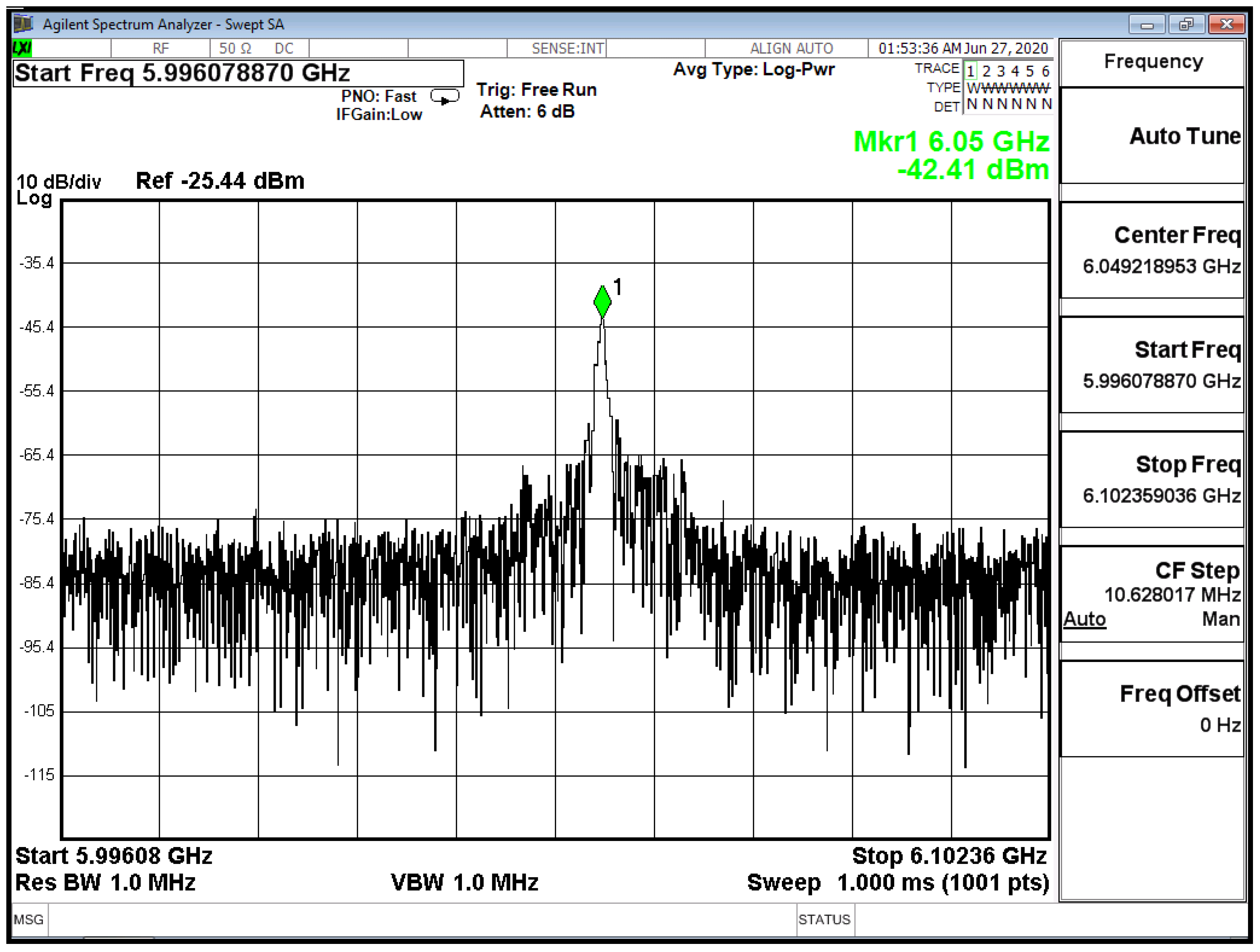
The fabricated PLL chip is tested using an on-wafer test setup. The PLL reference clock is provided by Keysight J-BERT N4903B. The PLL output is down-converted by a V-band sub-harmonic mixer, VDI WR15SHM, with a 30 GHz LO input. Figure 14 shows a close-in spectrum of the PLL output at f = 66.05 GHz with 515 MHz of the reference clock. The measured phase noise of the PLL is −84.43 dBc/Hz and −100 dBc/Hz, at 1 MHz and 10 MHz offset frequencies, respectively, as shown in Figure 15.
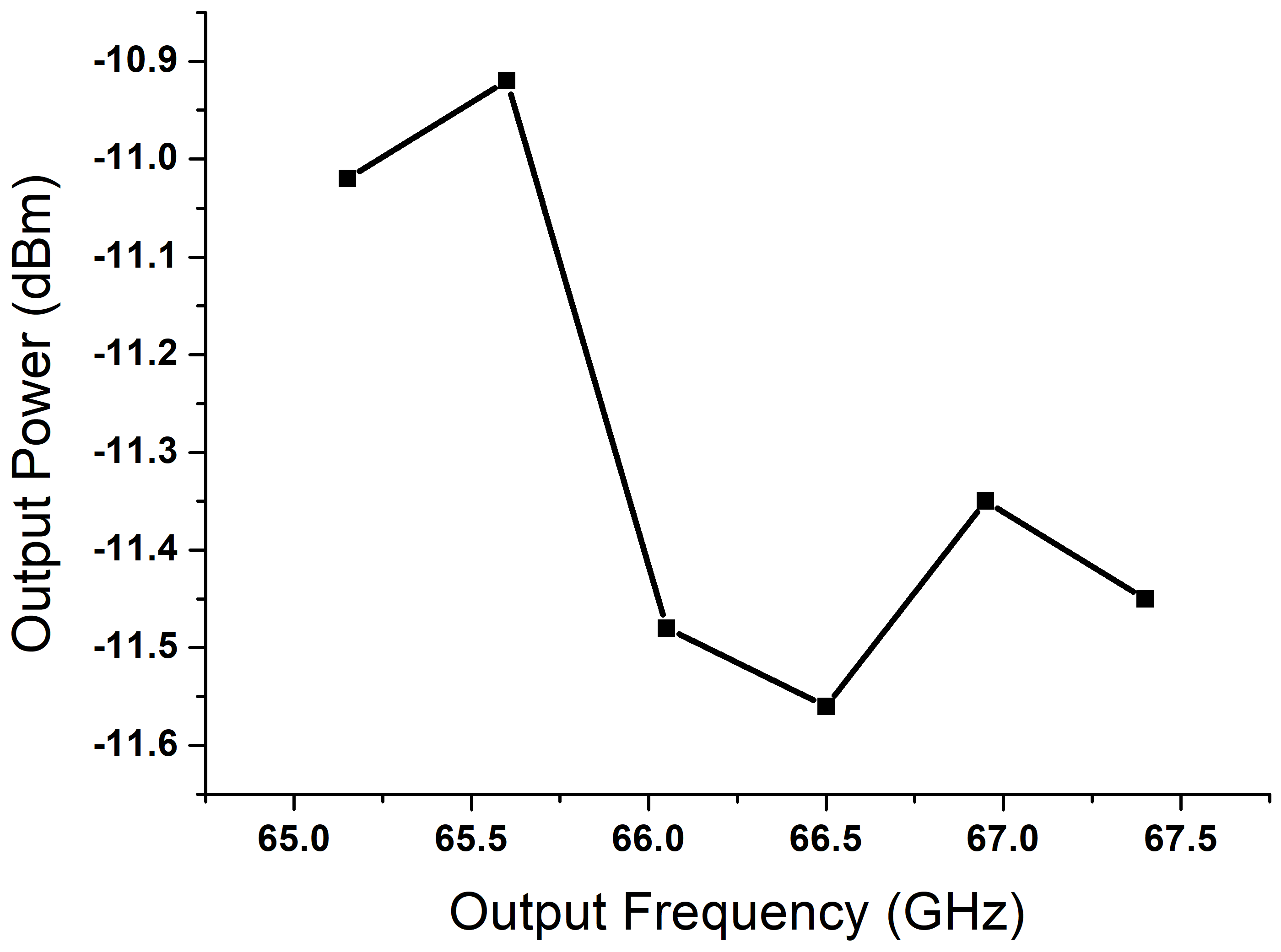
The output power of the PLL is measured using a V-band power sensor, Keysight N8488A, and a power meter, Keysight N1914A. The PLL achieves locking from 65.15 GHz to 67.4 GHz with the output power greater than −11.6 dBm, as shown in Figure 16. The measured PLL output frequency is lower than the simulation by 6–7 GHz, and the discrepancy is attributed to inaccuracies in EM modeling of layout parasitics and process variations. The PLL chip consumes 88 mW from a single 1.4 V supply. The optional PLL output at 2f was not tested due to the lack of spectrum and power testing capability at around 130 GHz. Table 1 compares the presented PLL with prior work. The PLL achieves an FoM 132.58 dBc/Hz. The locking range of the PLL can be improved with a capacitor bank based tuning network for a wider tuning range VCO and ILFD for better FoM. Table 2 compares the proposed PFD with prior work, where it is seen that the proposed PFD consumes relatively low power.
5. Conclusions
This paper presents a V-band PLL with a novel PFD circuit. A cross-coupled VCO has been used as an RF signal generator with dual-frequency outputs. The fundamental frequency output has been injected to ILFD for 2nd order division and to the RF output probing PAD. The ILFD has been implemented using cross-coupled topology in order to yield similar parasitic effects as VCO. A novel PFD was employed for its simplicity and low-power consumption. The PFD has been implemented with only four logic NOT gates in a combination of two controlled switches. This controlled switched technique reduces the glitches which improve the tuning voltage efficiency. The PLL is fabricated in a 65-nm LP CMOS process, and it achieves an FoM 132.58 dBc/Hz. The PLL measured output power is −11.6 dBm with a locking range of 65.15 GHz to 67.4 GHz and phase noise of −84.43 dBc/Hz at 1 MHz offset while consuming 88 mW DC power. The proposed PLL can be utilized as a frequency synthesizer for carrier signal generation in high frequency transceiver circuits.
Author Contributions
Circuit idea, W.A. and M.S.; circuit design/layout, W.A. and Z.M.; on-wafer testing, W.A. and Z.M.; writing—original draft preparation, W.A. and M.S.; writing—review and editing, W.A. and M.S.; All authors have read and agreed to the published version of the manuscript.
Funding
This research was funded by the Korea government(MSIT) (No. 2020-0-00960).
Acknowledgments
This work was supported by Institute of Information & communications Technology Planning & Evaluation (IITP) grant funded by the Korea government(MSIT) (No.2020-0-00960,Development of THz 3-dimensional beam-forming systems using distributed feeding of meta antenna for 6G mobile communication.)
Conflicts of Interest
The authors declare no conflict of interest.
References
- Kim, N.; Song, K.; Yun, J.; Yoo, J.; Rieh, J. Two 122-GHz Phase-Locked Loops in 65-nm CMOS Technology. IEEE Trans. Microw. Theory Tech. 2016, 64, 2623–2630. [Google Scholar] [CrossRef]
- Jain, S.; Zhang, N.; Belostotski, L. Millimeter-wave CMOS PLL using a push-push oscillator. In Proceedings of the IEEE 30th Canadian Conference on Electrical and Computer Engineering (CCECE), Windsor, ON, Canada, 30 April–3 May 2017; pp. 1–4. [Google Scholar]
- Tsai, K.; Liu, S. A 104-GHz Phase-Locked Loop Using a VCO at Second Pole Frequency. IEEE Trans. Very Large Scale Integr. VLSI Syst. 2012, 20, 80–88. [Google Scholar] [CrossRef]
- Shahramian, S.; Hart, A.; Tomkins, A.; Carusone, C.A.; Garcia, P.; Chevalier, P.; Voinigescu, S.P. Design of a Dual W- and D-Band PLL. IEEE J. Solid State Circuits 2011, 46, 1011–1022. [Google Scholar] [CrossRef]
- Chiang, P.; Wang, Z.; Momeni, O.; Heydari, P. A 300GHz frequency synthesizer with 7.9% locking range in 90nm SiGe BiCMOS. In Proceedings of the 2014 IEEE International Solid-State Circuits Conference Digest of Technical Papers (ISSCC), San Francisco, CA, USA, 9–13 February 2014; pp. 260–261. [Google Scholar]
- Zhao, Y.; Chen, Z.Z.; Du, Y.; Li, Y.; Hadi, R.A.; Virbila, G.; Xu, Y.; Kim, Y.; Tang, A.; Reck, T.J.; et al. A 0.56 THz Phase-Locked Frequency Synthesizer in 65 nm CMOS Technology. IEEE J. Solid State Circuits 2016, 51, 3005–3019. [Google Scholar] [CrossRef]
- He, J.; Xiong, Y.Z.; Li, J.; Hou, D.; Hu, S.; Yan, D.L.; Arasu, M.A.; Zhang, Y.P. A fully integrated 166-GHz frequency synthesizer in 0.13-μm SiGe BiCMOS for D-band applications. In Proceedings of the 2014 International Symposium on Integrated Circuits (ISIC), Singapore, 10–12 December 2014; pp. 156–159. [Google Scholar]
- Yeh, Y.; Lin, X.; Chang, H.; Chen, K. A V-band 65 nm CMOS low DC power low phase noise PLL using divide-by-three injection-locked frequency divider. In Proceedings of the 2016 IEEE International Symposium on Radio-Frequency Integration Technology (RFIT), Taipei, Taiwan, 24–26 August 2016; pp. 1–3. [Google Scholar]
- Chen, H.; Wang, T.; Lu, S. A Millimeter-Wave CMOS Triple-Band Phase-Locked Loop with A Multimode LC-Based ILFD. IEEE Trans. Microw. Theory Tech. 2011, 59, 1327–1338. [Google Scholar] [CrossRef]
- Parvais, B.; Scheir, K.; Vidojkovic, V.; Vandebriel, R.; Vandersteen, G.; Soens, C.; Wambacq, P. A 40 nm LP CMOS PLL for high-speed mm-wave communication. In Proceedings of the 2010 ESSCIRC, Seville, Spain, 13–17 September 2010; pp. 254–257. [Google Scholar]
- Xu, Z.; Gu, Q.J.; Wu, Y.; Jian, H.; Wang, F.; Chang, M.F. An integrated frequency synthesizer for 81–86GHz satellite communications in 65nm CMOS. In Proceedings of the 2010 IEEE Radio Frequency Integrated Circuits Symposium, Anaheim, CA, USA, 23–25 May 2010; pp. 57–60. [Google Scholar]
- Abedi, R.; Kananizadeh, R.; Esmaili, A.; Momeni, O.; Heydari, P. A 53–61GHz Low-Power PLL With Harmonic Positive Feedback VCO in 65nm CMOS. In Proceedings of the 2018 IEEE International Symposium on Circuits and Systems (ISCAS), Florence, Italy, 27–30 May 2018; pp. 1–5. [Google Scholar]
- Garg, S.K.; Singh, B. A novel design of an efficient Low Power Phase Frequency Detector for Delay Locked Loop. In Proceedings of the 2016 IEEE 1st International Conference on Power Electronics, Intelligent Control and Energy Systems (ICPEICES), Delhi, India, 4–6 July 2016; pp. 1–4. [Google Scholar]
- Ali, I.; Oh, S.J.; Abbasizadeh, H.; Rikan, B.H.; Rehman, M.R.U.; Lee, D.S.; Lee, K.Y. An ultra-low power fully synthesizable digital phase and frequency detector for ADPLL applications in 55 nm CMOS technology. In Proceedings of the 2017 13th International Conference on Emerging Technologies (ICET), Islamabad, Pakistan, 27–28 December 2017; pp. 1–6. [Google Scholar]
- Huang, Q.; Zhan, C.; Burm, J. A low-complexity fast-locking digital PLL with multi-output bang-bang phase detector. In Proceedings of the 2016 IEEE Asia Pacific Conference on Circuits and Systems (APCCAS), Jeju, Korea, 25–28 October 2016; pp. 418–420. [Google Scholar]
- Nasrollahpour, M.; Agrawal, P.; Sreekumar, R.; Yen, C.H.; Aldacher, M.; Ye, S.; Hamedi- Hagh, S. Design of a 65-69 GHz 1000:1 FMCW PLL in 65nm CMOS Technology. In Proceedings of the 2019 IEEE Texas Symposium on Wireless and Microwave Circuits and Systems (WMCS), Waco, TX, USA, 28–29 March 2019; pp. 1–5. [Google Scholar]
- Abdulaziz, M.; Forsberg, T.; Tormanen, M.; Sjoland, H. A 10-mW mm-Wave Phase-Locked Loop with Improved Lock Time in 28-nm FD-SOI CMOS. IEEE Trans. Microw. Theory Tech. 2019, 67, 1588–1600. [Google Scholar] [CrossRef] [Green Version]
- Kuncham, S.S.; Gadiyar, M.; Sushmitha, D.K.; Lad, K.K.; Laxminidhi, T. A Novel Zero Blind Zone Phase Frequency Detector for Fast Acquisition in Phase Locked Loops. In Proceedings of the 2018 31st International Conference on VLSI Design and 2018 17th International Conference on Embedded Systems (VLSID), Pune, India, 6–10 January 2018; pp. 167–170. [Google Scholar]
- Ahmad, A.A.; Ali, S.H.M.; Kamal, N.; Abdul Rahman, S.R.; Othman, M. Design of Phase Frequency Detector (PFD), Charge Pump (CP) and Programmable Frequency Divider for PLL in 0.18um CMOS Technology. In Proceedings of the 2018 IEEE International Conference on Semiconductor Electronics (ICSE), Kuala Lumpur, Malaysia, 15–17 August 2018; pp. 242–245. [Google Scholar]
- Jandhyala, S.; Tapse, S. A power efficient phase frequency detector and low mismatch charge pump in on-chip clock generator. In Proceedings of the 2016 IEEE Distributed Computing, VLSI, Electrical Circuits and Robotics (DISCOVER), Mangalore, India, 13–14 August 2016; pp. 57–61. [Google Scholar]
- Kumar, N.; Kumar, M. Design of low power and high-speed phase detector. In Proceedings of the 2016 2nd International Conference on Contemporary Computing and Informatics (IC3I), Noida, India, 14–17 December 2016; pp. 676–680. [Google Scholar]
Figure 1.
Block diagram of Proposed phase-locked loop (PLL).

Figure 2.
(a) Schematic of proposed voltage-controlled oscillator (VCO), (b) Simulated tuning range w.r.t tuning voltage.
Figure 2.
(a) Schematic of proposed voltage-controlled oscillator (VCO), (b) Simulated tuning range w.r.t tuning voltage.

Figure 3.
(a) Schematic of injection-locked frequency divider (ILFD), (b) Sensitivity curves of ILFD.
Figure 3.
(a) Schematic of injection-locked frequency divider (ILFD), (b) Sensitivity curves of ILFD.

Figure 4.
Schematic of current-mode logic (CML) Divider.

Figure 5.
Phase-frequency detector (PFD) Architecture: (a) Conventional PFD and (b) Sub-sampling PD.
Figure 5.
Phase-frequency detector (PFD) Architecture: (a) Conventional PFD and (b) Sub-sampling PD.

Figure 6.
D flip-flop (D-FF) circuit schematic.

Figure 7.
AND-gate schematic.

Figure 8.
Schematic of the proposed PFD: (a) up-pulse and (b) down-pulse generator.

Figure 9.
PFD Operating Characteristics: (a) dead-zone free (ideal), (b) dead-zone exists and (c) dead-zone free (proposed).
Figure 9.
PFD Operating Characteristics: (a) dead-zone free (ideal), (b) dead-zone exists and (c) dead-zone free (proposed).

Figure 10.
Comparison of the conventional and proposed PFD.

Figure 11.
Schematic of CP and LF.

Figure 12.
Stack information of Substrate configuration.

Figure 13.
Chip Photograph of the PLL (chip area without pads estimated from chip photo) (active chip size: 0.68 × 0.54 mm).
Figure 13.
Chip Photograph of the PLL (chip area without pads estimated from chip photo) (active chip size: 0.68 × 0.54 mm).

Figure 14.
Measured output spectrum of the PLL at = 66.05 GHz (uncalibrated).

Figure 15.
Measured phase noise of the PLL at f = 66.05 GHz.

Figure 16.
Measured output power of the PLL.


Table 1.
Comparison of recently published millimeter-wave PLL.
| Parameter | [8] | [9] | [10] | [11] | [12] | [16] | [17] | Our Work |
|---|---|---|---|---|---|---|---|---|
| Technology (nm) | 65 | 90 | 40 LP | 65 | 65 | 65 | 28 | 65 LP |
| Frequency (GHz) | 58.5–58.9 | 60.2–62.4 | 63–70 | 70–78 | 53–61 | 65–69 | 54.1–57 | 65.15–67.4 |
| Supply Voltage (V) | 1.2 | 1.5 | 1.1 | 1 | 0.8 | 1.2 | - | 1.4 |
| PN@1MHz (dBc/Hz) | −83.5 | −69.92 | −85 | −83 | −88 | −98.5 ** | −93 | −84.43 |
| Ref. Frequency (MHz) | 150 | 78 | - | - | 56 | 67 | 2280 | 515 |
| Power Consumption (mW) | 43 | 106.6 | 79.2 | 65 | 48 | 72.44 | 10 | 88 |
| Active Chip Area (excluding pads) () | 1 * | 1.12 * | 0.192 | 0.31 | 0.32 | 3.24 * | 0.19 | 0.37 |
| Output Power (dBm) | −14 | −9.5 | - | - | - | - | - | −11.6 |
| FOM (dBc/Hz) | 119.16 | 116.5 | 142.9 | 142.9 | 148.6 | 152.58 | 152.24 | 132.58 |
*: with Probing Pads. **: From Simulations
© 2020 by the authors. Licensee MDPI, Basel, Switzerland. This article is an open access article distributed under the terms and conditions of the Creative Commons Attribution (CC BY) license (http://creativecommons.org/licenses/by/4.0/).
Share and Cite
MDPI and ACS Style
Abbas, W.; Mehmood, Z.; Seo, M. A V-Band Phase-Locked Loop with a Novel Phase-Frequency Detector in 65 nm CMOS. Electronics 2020, 9, 1502. https://doi.org/10.3390/electronics9091502
AMA Style
Abbas W, Mehmood Z, Seo M. A V-Band Phase-Locked Loop with a Novel Phase-Frequency Detector in 65 nm CMOS. Electronics. 2020; 9(9):1502. https://doi.org/10.3390/electronics9091502
Chicago/Turabian StyleAbbas, Waseem, Zubair Mehmood, and Munkyo Seo. 2020. "A V-Band Phase-Locked Loop with a Novel Phase-Frequency Detector in 65 nm CMOS" Electronics 9, no. 9: 1502. https://doi.org/10.3390/electronics9091502
Note that from the first issue of 2016, this journal uses article numbers instead of page numbers. See further details here.