
Designing a Twin Frequency Control DC-DC Buck Converter Using Accurate Load Current Sensing Technique


1
College of Engineering, Science and Environment, University of Newcastle, Callaghan, NSW 2308, Australia
2
School of Electrical and Electronic Engineering, Nanyang Technological University, Singapore 639798, Singapore
*
Authors to whom correspondence should be addressed.
Electronics 2024, 13(1), 45; https://doi.org/10.3390/electronics13010045
Submission received: 1 December 2023
/
Revised: 18 December 2023
/
Accepted: 19 December 2023
/
Published: 20 December 2023
(This article belongs to the Special Issue Advances in SoCs and Embedded Systems)
Abstract
:In this paper, a buck DC-DC converter with the proposed twin frequency control scheme (TFCS) and accurate load current sensing (ALCS) was designed and implemented with 0.18 µm CMOS technology for a supply voltage ranging from 2.0 to 3.0 V, which is compatible with state-of-the-art batteries (NiCd/NiMH: 1.1–2 V, Li-Ion: 2.5–4.2 V). The proposed converter yields a peak efficiency of about 92.7% with a load current of 30 mA. Furthermore, it only occupies a silicon area of 1.3 mm2. The proposed buck converter is dedicated for smartphone applications whereby it spends most of its time in idle, low load conditions.
1. Introduction
Modern 4G smartphones are embedded with a high-speed multi-core processor, gigabytes of flash memory, high-resolution color display, 3G/4G and Bluetooth wireless communication devices [1]. Therefore, the quiescent power consumption of a smartphone is comparable to a laptop or a handheld tablet. Furthermore, new modern applications such as live video streaming require a constant utilization of an LED backlight display or cloud computing services, which will no doubt increase the total power consumption drastically [2]. All of the above enhanced functionalities of a 4G smartphone will heighten the pressure on the battery lifetime and escalate the urgency for a more efficient power management system [3]. However, the NiCd/NiMH and Li-ion batteries, which are widely used to provide a source of power, are very limited in supplying the energy and power demands for the wide variety of applications found in a smartphone. This is supported by a recent research study which has shown that its energy density has only doubled over the past decade from 300 to 600 Whr/liter [4]. Hence, the viable solution is to reduce the overall battery power consumption by improving the power efficiency of the power management unit (PMU) in a smartphone.
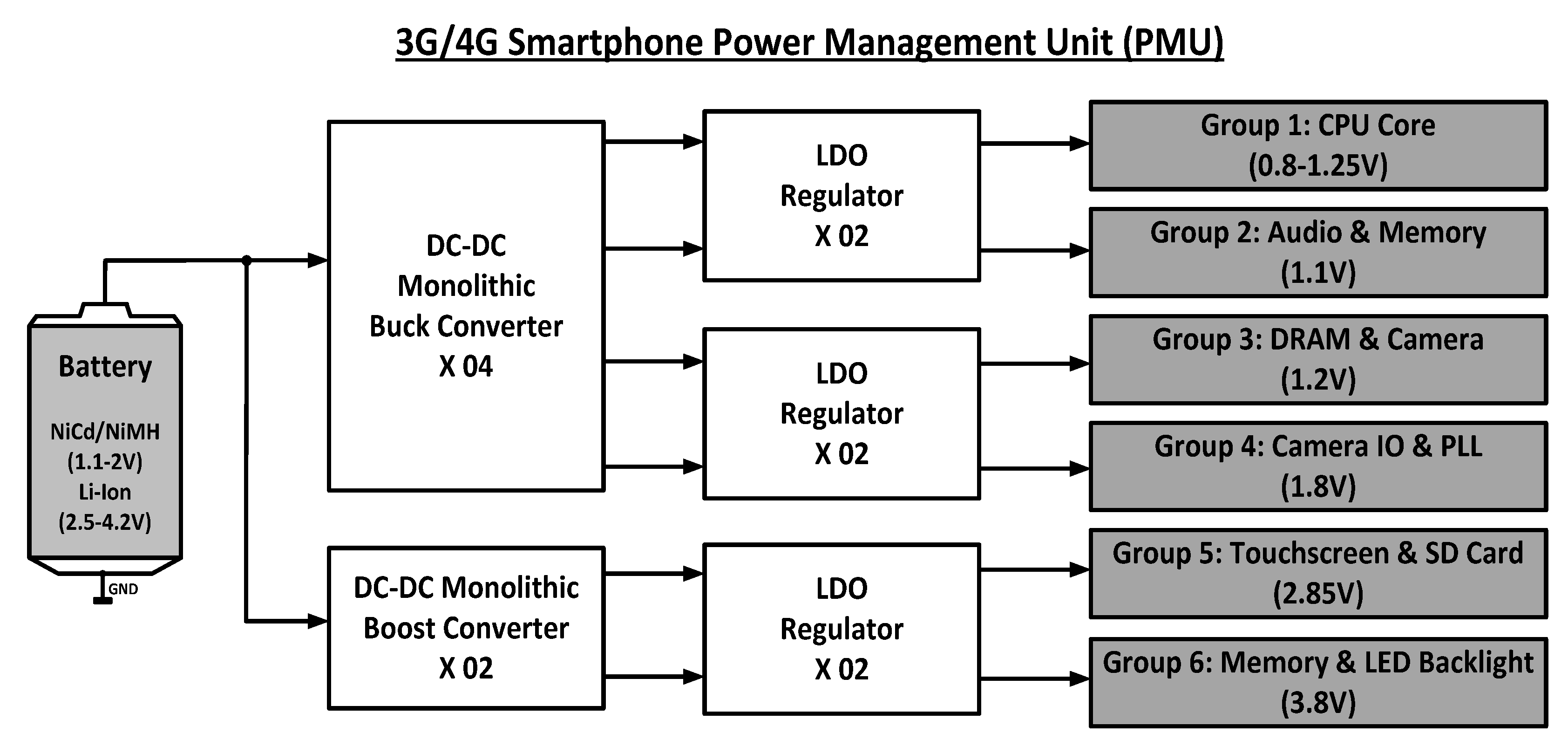
For the past few years, there have been numerous interesting research works [5,6] which have presented various power consumption usage models for 3G/4G smartphones. Modern power management systems in smartphones [7] are used to generate a constant or variable output voltage supply from battery sources which have a wide input range variation, e.g., NiCd/NiMH, 1.1–2 V, or Li-Ion, 2.5–4.2 V [8,9]. Power converters (buck/boost) are indispensable building blocks found in a part of the power management unit (PMU) of a smartphone, as shown in Figure 1. Their objectives are to supply a well-regulated supply voltage to the different group core modules [1] found in a smartphone. A full illustration of the PMU of a smartphone can be found here [10].
The key to prolonging the battery lifetime is to improve the power efficiency of the DC-DC converter. Since a smartphone spends most of its time in the low load condition [2], numerous research works [11,12,13,14] have already aimed to improve the light-load efficiency as the core priority. Though the new circuit implementation is novel, improvements in power efficiency are minimal, and the proposed circuit techniques are relatively complex. One of the more interesting works proposed [15] a width-switching scheme whereby the width of the respective power transistors can be altered according to the load current demand. However, the light-load efficiency falls below 80% for <20 mW of load power. In another study [16], pulse-skipping modulation (PSM) was added in between PWM and PFM to ensure a seamless transition of the power efficiency curve from a low to high load current. This technique is well known as the tri-hybrid mode converter, which can deliver high efficiency for a wide load range. On the other hand, it has drawbacks, too. Whenever it transits to PSM mode, load regulation is always sacrificed, and the power conversion efficiency is only maximized in several load conditions. Lastly, tri-hybrid mode control requires several modulators with complex-mode switching circuits, which may lead to stability issues, e.g., inductor runaway.
Hence, in this current research work, a twin frequency control scheme (TFCS), together with an accurate load current sensing block (ALCS), are proposed to achieve high efficiency under a low load condition (<50 mW) regardless of the process/power transistor variation as well as the source voltage or load current variation. This is compatible with the fact that smartphones drive these ranges of power load levels during their idle conditions. For proof of concept, a monolithic buck converter with the proposed TFCS and ALCS are implemented and tested. Furthermore, a conventional PWM/PFM buck controller is implemented to provide a good comparison with our proposed work. The design and measurement details are presented in this paper in the following structure: Section 2 discusses the operation of the system and block level design. Section 3 presents the experimental results, followed by a discussion and comparison with the state-of-the-art works, as summarized in Table 1. Finally, the conclusion will be shown in Section 4.
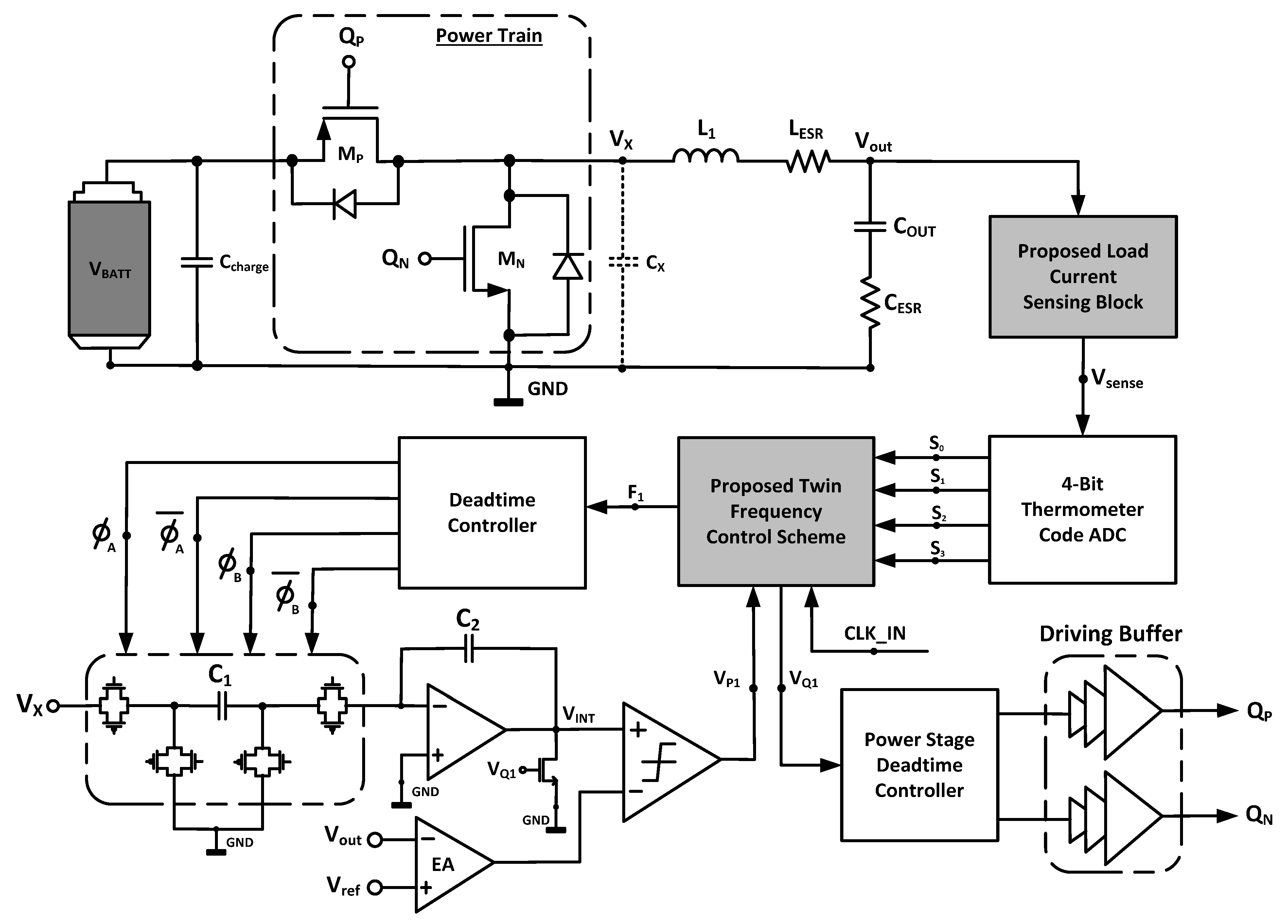
2. Proposed Twin Frequency Control DC-DC Buck Converter
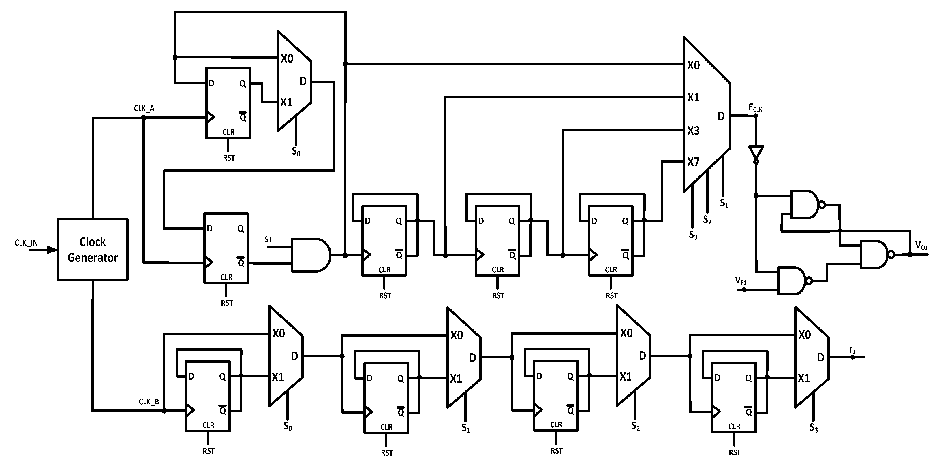
Our proposed work, shown in Figure 2, consists of a twin frequency control scheme (TFCS), an accurate load current sensing (ALCS) block, a switched capacitor (SC) integrator, two deadtime controllers and the power train stage. In general, the output voltage, Vout, gives important information about the load current, and this will be sensed by the proposed load current sensing block to produce a sensing voltage, Vsense. Furthermore, this voltage, in turn, is compared with a 4-bit thermometer code ADC to produce a 4-bit signal (S0, S1, S2 and S3). This gives an accurate indication of the load current level drawn by the output of the DC-DC converter. The 4-bit signal goes through the TFCS, which yields two non-overlapping clocks to control the switches in the switched-capacitor integrator and also a clock frequency to reset the integration cycle. In other words, it is meant to define the switching period of the buck converter. The integrated voltage, Vint, monitors Vx, which gives an indication of the output load current and its corresponding voltage level. The integrated voltage, Vint, can be derived as follows:
where Vint is the integrated voltage and the output of the SC integrator. is the frequency of the switches in the SC integrator, and is the ratio of the capacitor, which gives the gain of the amplifier. refers to the input voltage of the DC-DC buck converter. and Ts refer to the integration and switching period of the converter, respectively.
With reference to Equation (3), it is evident that the ratios of capacitors are constant under any circumstances such as heavy or light load. The remaining parameters, except , are variables which will change according to the DC load power drawn by the output of the converter. Specifically, in a light load condition, the above-mentioned 4-bit signal (S0, S1, S2 and S3) will activate the proposed TFCS. This will alter the switching frequency of the DC-DC converter and the corresponding switches in the SC integrator. Hence, the switching losses of the buck converter will be significantly reduced in a low current load condition. This will improve the power efficiency for the load range (<50 mW) where the smartphone is idling.
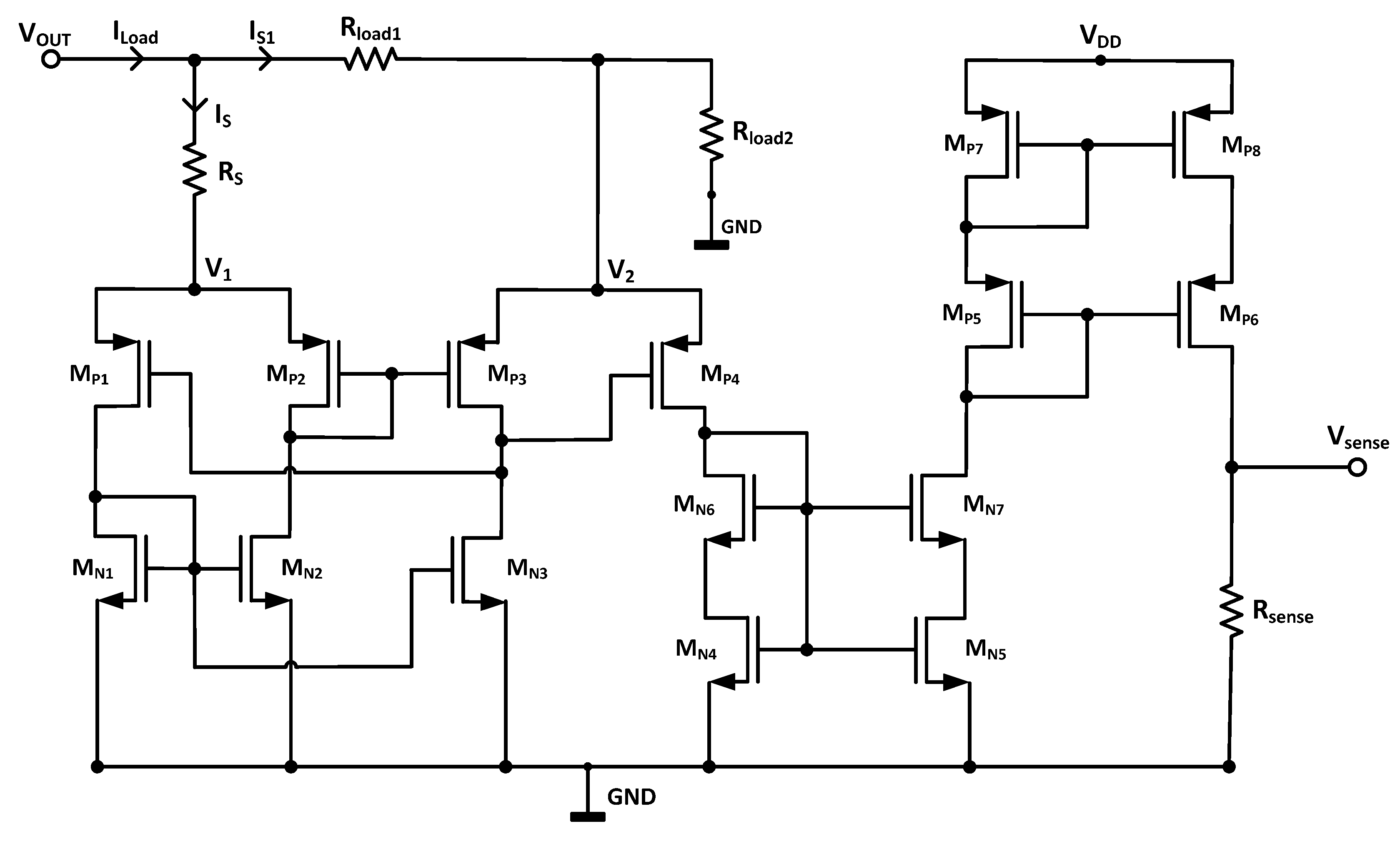
2.1. Proposed Accurate Load Current Sensing (ALCS) Block
The proposed ALCS, shown in Figure 3, is an extension and improvement to a prior work [20]. A more in-depth analysis with regard to the prior work of current sensing techniques will be presented in Appendix A. It is used to sense the load current and gives an output sense voltage, Vsense, via the sensing resistor, Rsense. This voltage level is proportional to the load current level. Transistors MP1–MP4 and MN1–MN3 form a current conveyor structure where negative feedback is employed, which forces the node voltage V1 to be equal to V2 at a balanced state equilibrium. If the V2 node increases, the drain voltage of the MP3/the gate voltage of MP1 will increase since the transistor MN1 will force the mirrored current going through MN3 to be the same. This action allows for a larger net current to go through MP2, which becomes mirrored over to MP3. Hence, the gate voltage of MP3 decreases, which pulls node voltage V3 down. This constitutes negative feedback and forces V2 to be equal to V1. At the same time, the cascode pair, MP5 and MP6, is included to increase the output impedance of the current mirror formed by MP7 and MP8. This will ensure a more accurate mirroring of the current, behaving more like an ideal current source. Thus, transistors MN6–MN7 are stacked on top of MN4–MN5 to form a diode-connected configuration. This is at the expense of MN4–MN5 being biased in the linear triode region, with a larger transistor length value.
Assume V1 to be equal to V2:
Substitute Equation (6) into (7) to obtain
The output voltage, Vout, can be derived as follows:
If the ratio of the resistance Rload1/RS << 1, Equation (8) becomes
At the same time, Equation (9) is simplified as
whereby Rload,total = Rload1 + Rload2.
The above derivation proves that the two passive resistors, Rload1 and Rload2, contribute to the total load resistance without excessive power dissipation, which will degrade the power efficiency of the overall DC-DC buck converter. Furthermore, the current, Is, going through Rs is negligible, having minimal impact on the overall power efficiency. Hence, the sense voltage, Vsense, can be derived to be
Substituting Equation (6) into (12) obtains the following:
If the ratio of the resistance Rload1/RS = ,
where is a constant.
The above derivation of the sense voltage, Vsense, can be used to provide a voltage that is proportional to the load current. The power dissipation across the passive sensing resistor, Rsense, is negligible as the current, Is, going through it is minimal. However, this sensing technique may have some drawbacks.
The above derivation and working operation assume that the output voltage, Vout, is a constant value. But, in fact, there are some AC ripples riding on it. This is caused by the product of the inductor current ripple and the ESR of the output filtering capacitor. Thus, to ensure a more accurate load current sensing capability, the inductor value is made relatively larger to reduce the ripples riding on the output voltage. Furthermore, trimming techniques are employed for the resistor, Rsense, as its value may differ by ±20% after the process of die fabrication. Therefore, careful consideration has to be taken into account when designing the next block as the resistor’s value due to the process, and the voltage supply and temperature (PVT) variation should never exceed the 1-bit resolution of the ADC stage. The W/L sizing of each transistor is shown in Table 2.
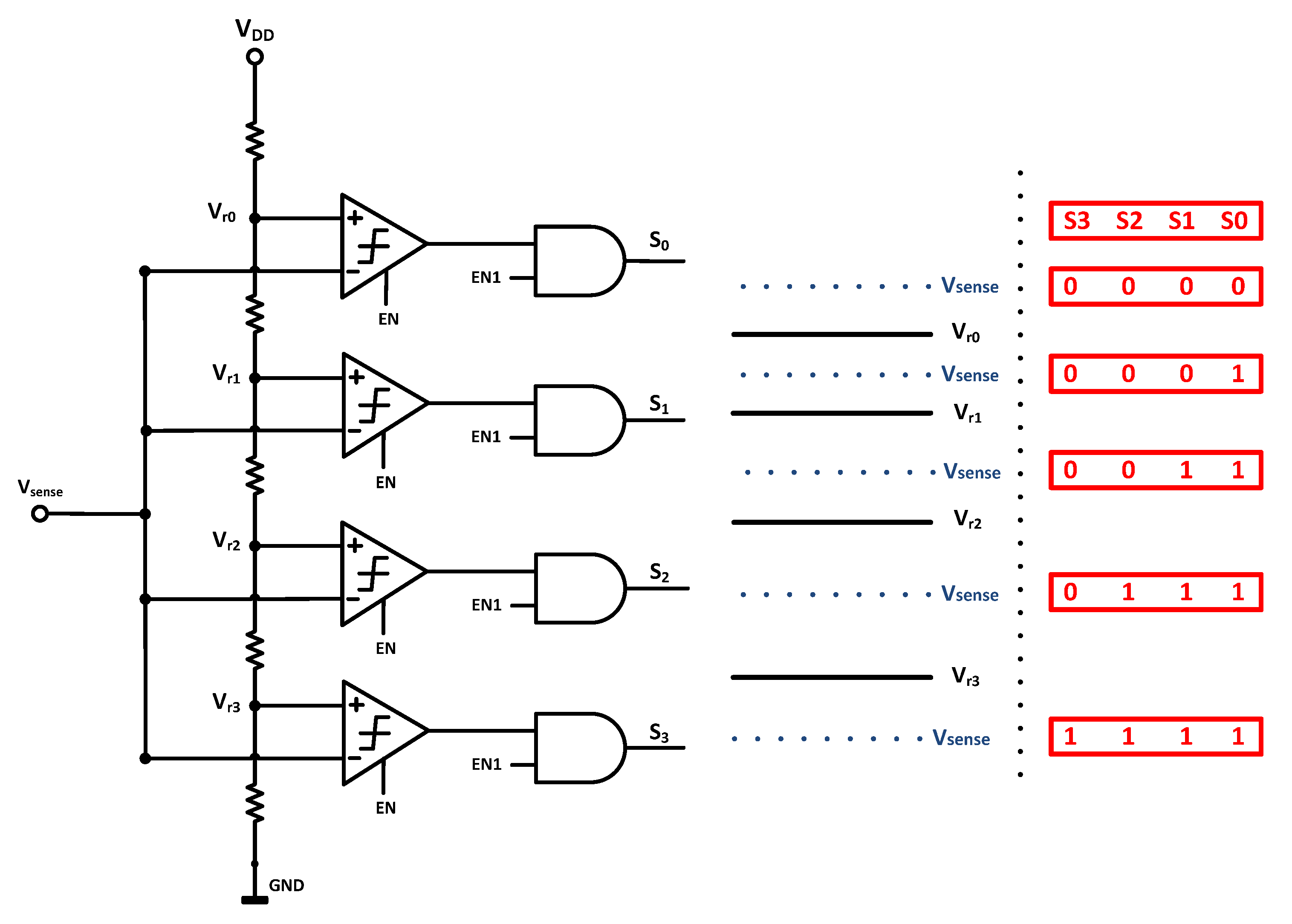
2.2. Four-Bit Thermometer Code ADC
The 4-bit thermometer code ADC, shown in Figure 4, is employed to compare the sense voltage, Vsense, with four voltage levels (Vr0, Vr1, Vr2 and Vr3) to generate a 4-bit thermometer code signal (S0, S1, S2 and S3). This gives vital information about the current load level. There are basically four different levels (0001, 0011, 0111 and 1111) which correspond to four different light load conditions. The resolution of the load current level can be improved at the expense of increasing the no. of comparators in the ADC, which will increase conduction and switching losses that may degrade the power efficiency. Hence, there exists a tradeoff between better resolution and power efficiency.
2.3. Proposed Twin Frequency Control Scheme (TFCS)
The proposed TFCS, shown in Figure 5, is used to progressively alter the switching frequency of the buck controller and the integration cycle according to the load current, which is embedded in the 4-bit signal level (S0, S1, S2 and S3). There are only four possible signal levels (0001, 0011, 0111 and 1111) which correspond to four different load current levels in the light, idle condition of a smartphone (<40 mA). As mentioned, the resolution of the load current level can be improved further, but at the expense of increased power consumption. Hence, there exists an optimum value for the no. of levels of load current associated with the signal generated by the thermometer code ADC.
2.4. Power Train
The power train consists of one PMOS (MP) and NMOS (MN) device, as shown in Figure 2. Both are 3.3 V transistors, which have a thicker gate oxide and occupy a much larger area than a regular transistor. Considering the power NMOS transistor, MN, the total power loss comprises the sum of the switching and conduction loss as follows:
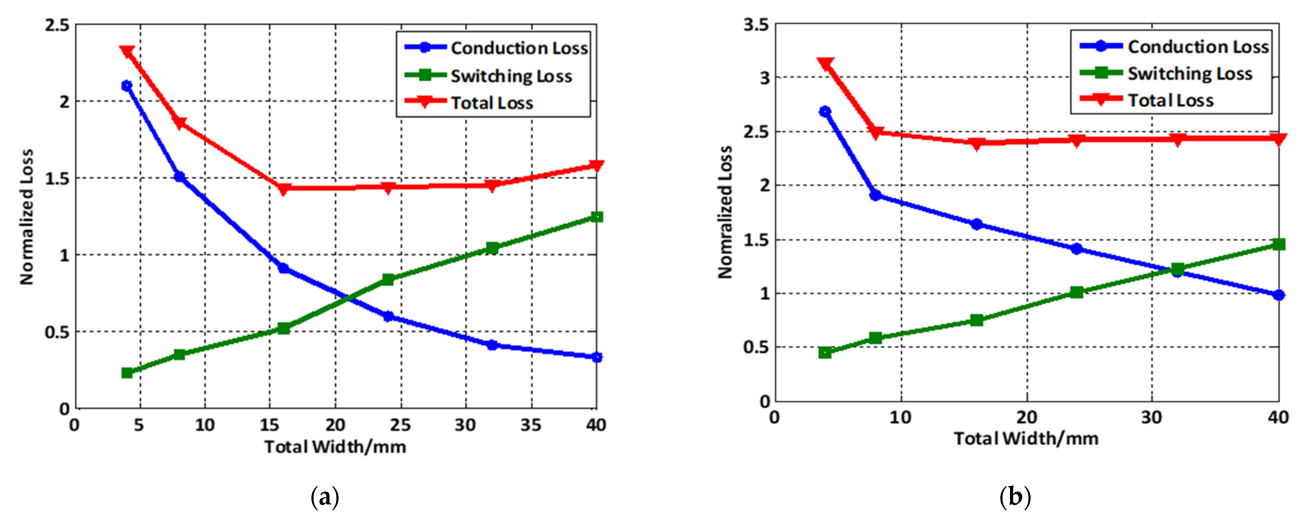
whereby Cgdn, Cgsn and Cdbn refer to the respective parasitic capacitance per unit width of the device, VBATT is the input voltage to the buck converter, fs refers to the switching frequency of the power train, Ron,N/WN is the on-resistance per unit width, IN refers to its RMS current and VN is the gate voltage of the power NMOS transistor. Thus, the optimum width, Wopt,N, can be calculated when the switching loss is equal to the conduction loss, given by
The optimized width for both the power NMOS and PMOS is shown in Figure 6, where the graph of the switching loss intersects the conduction loss. The graph plot is based on the highest load current of 40 mA and a switching frequency of 1 MHz. The aspect ratio and the on-resistance of the power transistors are shown in Table 1. In addition, the on-resistance and input parasitic capacitance required to calculate the conduction and switching loss, respectively, are the sum of the simulation results and a theoretical calculation of the resistance/capacitance of metal routing/contact/via and the silicon area occupied by the layout of the power train. Since the optimized width was finalized, it is now vital to find the best layout structure of the power train for our research application.
The efficiency of the power train is vital and depends largely on the layout structure, which is a compromise between the total gate charge (Qg) and the on-resistance (Ron) of the power transistors [21]. This is because the area (W·L) of the power transistor is proportional to the total gate capacitance but inversely proportional to the on-resistance of the power transistor. Recent research [22] proves that power transistors, which do not take into account the resistance and parasitic capacitance of metal routing, will have an error variation of more than 50% in the calculation of Qg and Ron. This is because the impact of the parasitic capacitance and resistance from layers of metal interconnection is extremely dependent upon the layout style of the power transistors and the positioning of its external source/drain connections. At the same time, the Ron value is greatly affected by the distributed parasitic resistance associated with metal interconnects to the source and drain terminals. Many past research efforts [23,24,25] aimed at improving and optimizing the layout of the power transistor to minimize the parasitic resistance and capacitance.
Traditionally, power transistors were designed with a multi-finger layout structure to maximize the channel width per unit area, which increases the current handling capability. On the other hand, a regular waffle layout structure was introduced [24] to further optimize the width per area ratio by having four neighboring transistors, enclosing a centralized localized one. However, the above-mentioned layout structure does not yield the best optimum tradeoff between the total gate capacitance (Qg) and the on-resistance (Ron). Thus, in a recent research work, there was an interesting proposal for a hybrid waffle layout structure [26,27], which proves that it can best optimize the tradeoff between the area, total gate charge and on-resistance.
However, in this research work, the above-mentioned hybrid waffle layout may not be suitable, as this buck converter is not operating at an extremely high frequency (>100 MHz). Hence, our proposed layout is a tapered/matrix structure, as shown in Figure 7, as it can provide a more uniform distribution of the DC current among the fingers of the transistor. In addition, the fingers of the power transistor are designed in a diagonal way, which will reduce the on-resistance and equalize the flow of current on the opposite side of the device. Furthermore, the nos. of fingers and multipliers for each power transistor are optimized, as shown in Table 1, so as to balance the tradeoff between the total gate charge and parasitic interconnection resistance. One of the drawbacks is that there is a “hotspot” at the corner, furthest away from the center of the power train. During measurement testing, this “hotspot” may increase the on-resistance of the power transistor, leading to an increase in the heat dissipation and ultimately degrading the power efficiency. Therefore, the die package must be thermally enhanced to avoid the overheating of the silicon die chip or create other reliability issues. However, for our work, it focuses on a smartphone idling state (low load power); hence, the above-mentioned drawback may not be significant.
3. Experimental Results
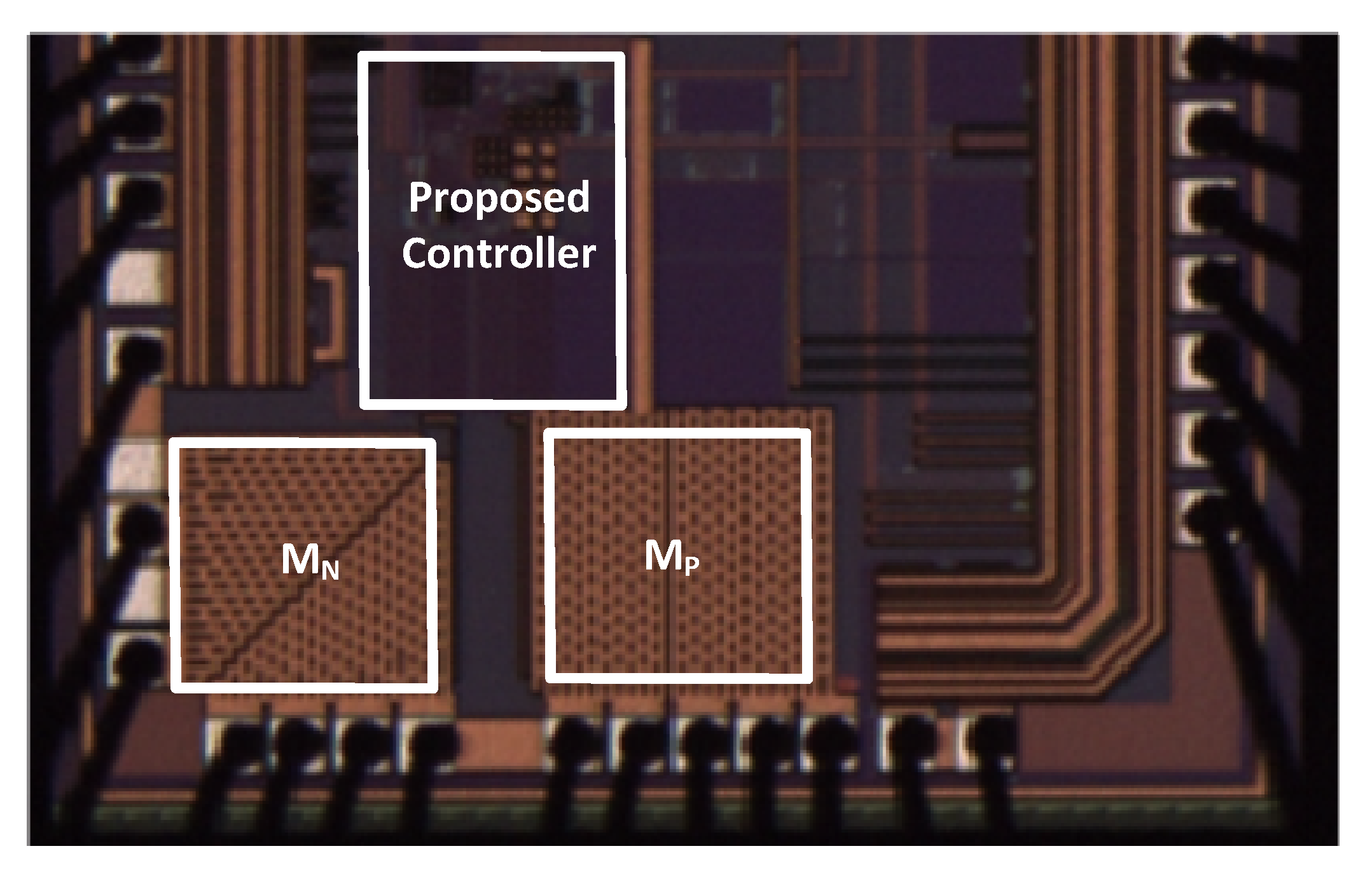
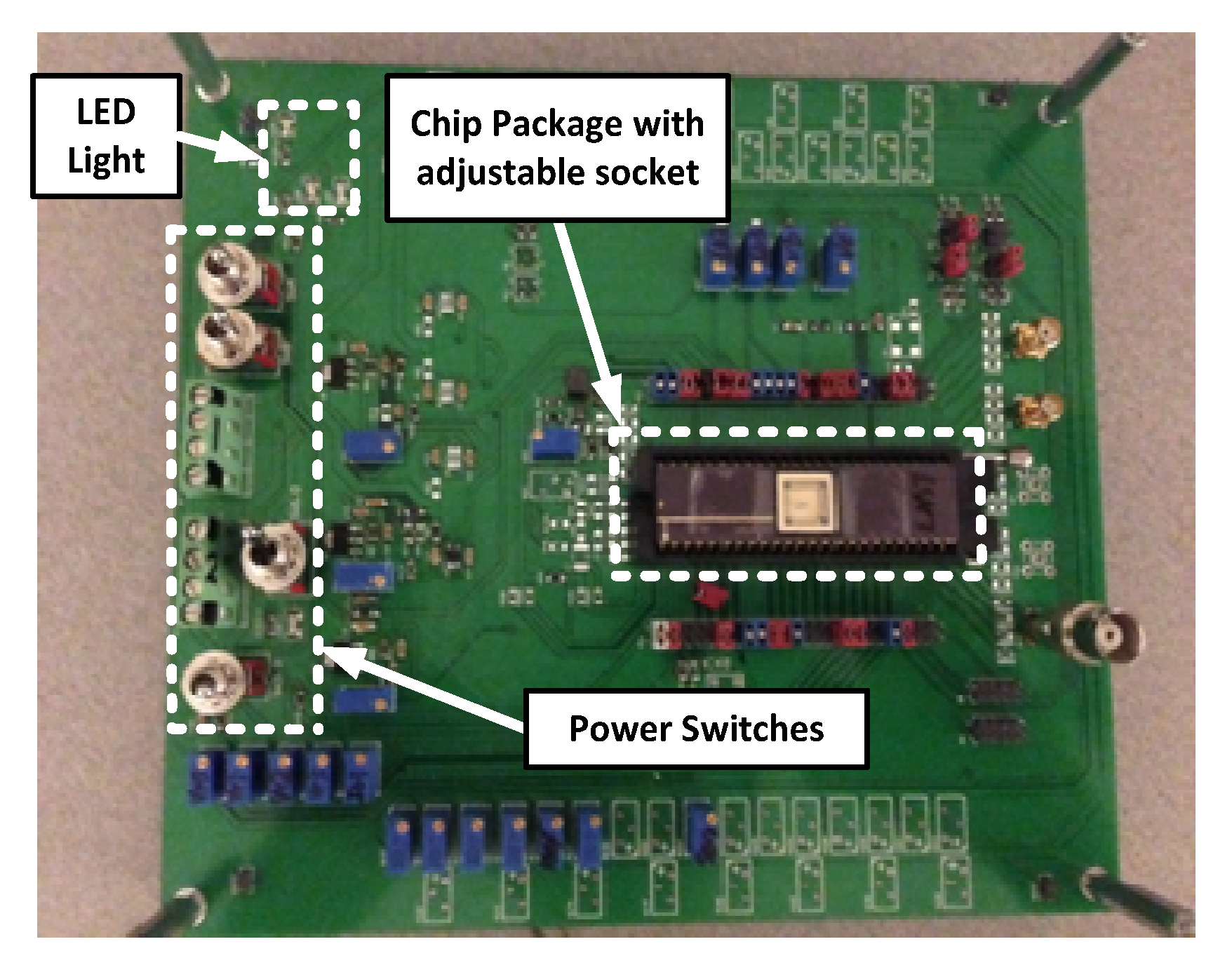
A buck DC-DC converter with the proposed TFCS and ALCS was implemented with 0.18 µm 1P6M CMOS technology with an area of 1.3 mm2. The micrograph of the chip is shown in Figure 7. The 2~3 V input and 1.25 V output buck converter utilizes an off-chip SMD 47 µH inductor (Coilcraft Shielded 1812PS Series) with a DCR of <1.0 Ω and a self-resonant frequency (SRF) of 17 MHz. A relatively larger value of an inductor value is selected to reduce the inductor ripple to <50% of the maximum load current. Furthermore, an output off-chip SMD ceramic 10 µF filtering capacitor (AVX Hi-Cap MLCC) has an estimated ESR of ~0.5 Ω. The capacitor type is chosen to be an SMD ceramic capacitor since it is the most inexpensive type compared to tantalum or aluminum electrolytic ones. However, the tradeoff comes with the relative larger value of ESR, which will lead to a larger peak-to-peak ripple riding on the output voltage of the buck converter. Thus, relatively larger values of the inductor and capacitor are chosen so as to mitigate the ripple problem. Furthermore, this helps to yield a more accurate sensing of the load current, as previously mentioned. Take note that the choice for the type of capacitor varies, depending on the application specification. A prototype of the buck converter with the TFCS and ALCS chip is also presented in Figure 8. It can be observed that our proposed work uses the DIP package with 48 leads. During testing, this is held tightly by the adjustable socket shown in Figure 8.
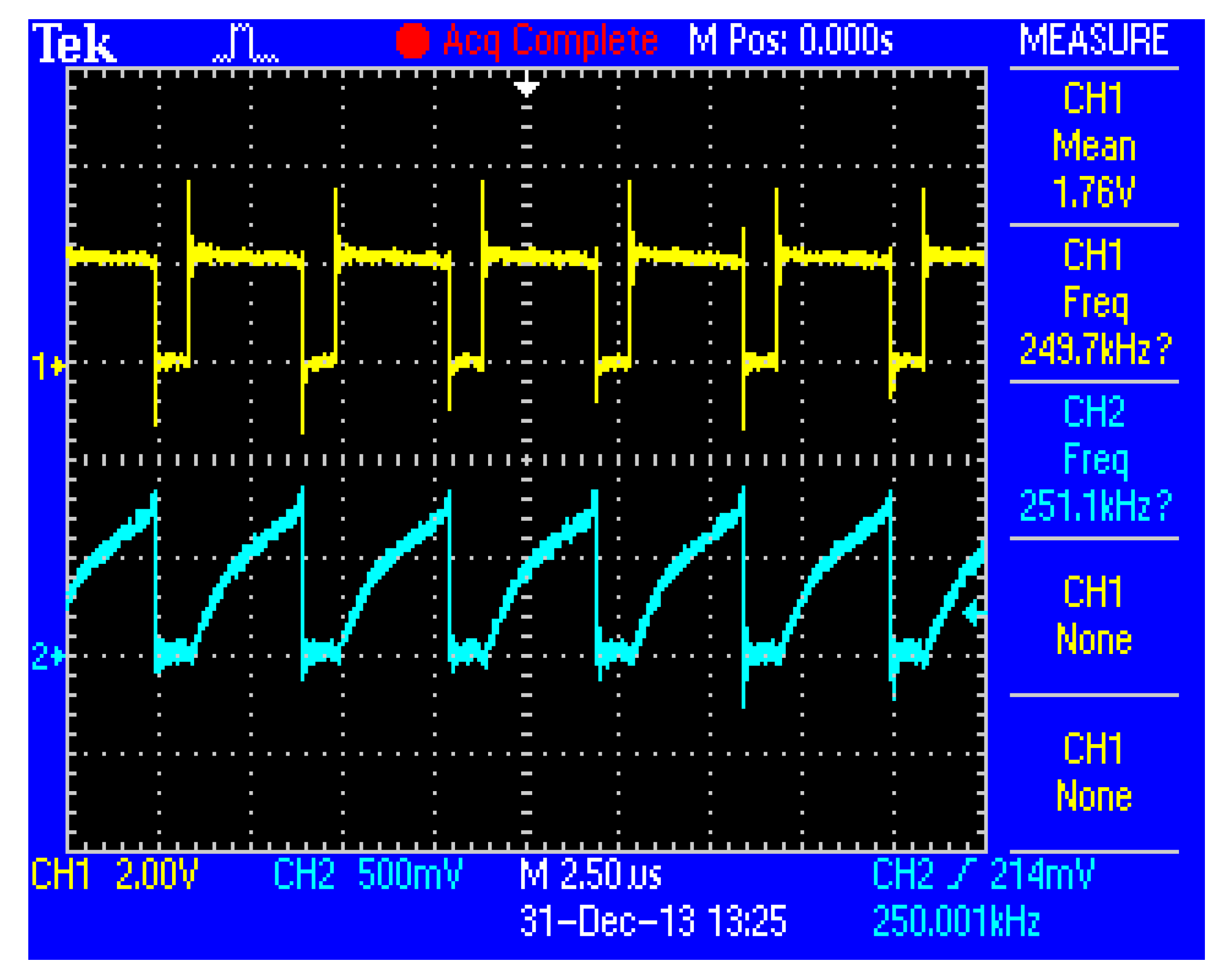
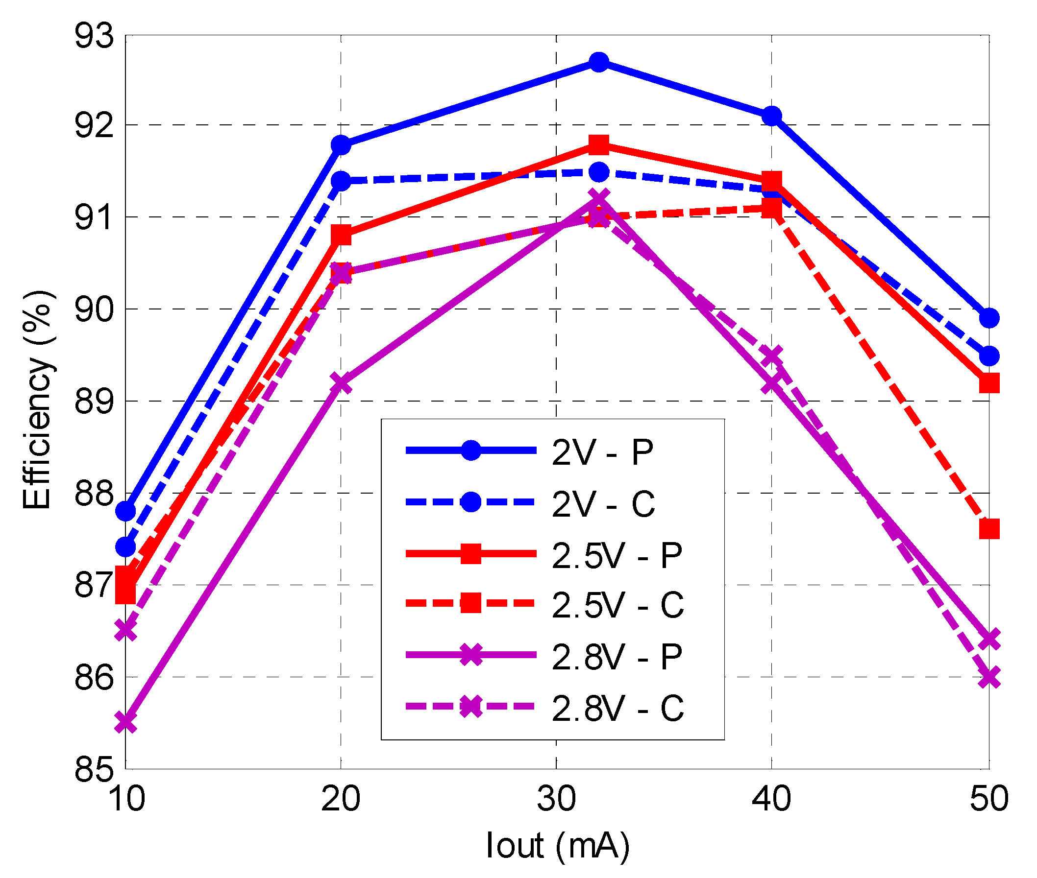
The performance evaluation is carried out in three general steps: (1) the performance of our proposed TFCS and ALCS is examined in light loading conditions, (2) a comparison of the power efficiency is made between our proposed work and the conventional PWM/PFM controller and (3) the design specification and performance comparison are summarized in Table 1. The proposed TFCS and ALCS allow the frequency to be reduced under different low load conditions. It achieves a peak efficiency of 92.7%, operating at 250 kHz with VBATT = 2 V, VOUT = 1.25 V and ILOAD = 30 mA, as shown in Figure 9. The top waveform is the voltage Vx, while the bottom one shows the integrated voltage Vint. This proves that our proposed TFCS and ALCS buck converter is stable and achieved high efficiency under the low load condition. However, taking a closer look at the Vx waveform, there is a significant interval whereby there are body diode conduction losses which degrade the power efficiency. This is because our proposed buck converter uses a fixed deadtime controller. One of our current and future works has therefore included a novel deadtime controller. Furthermore, from Figure 9, it is evident that our proposed controller does not enter DCM operation in a light load condition. The rationale is that for DCM operation, the node, Vx, will oscillate when both the power transistors are idling. This is due to the existence of the LC tank formed by the inductor and the parasitic capacitance at that node. Thus, this will incur additional power losses. Recent research efforts have included another free-wheeling switch [9,28,29] to dampen the sub-harmonic oscillation. However, this will incur an additional silicon area, as the aspect ratio of the additional switch is comparable to the size of a power transistor. Furthermore, it adds complexity to the circuit design, as another control signal has to be included to determine the turning on/off of this free-wheeling switch. Therefore, our proposed work uses a relatively larger inductor value to reduce the ripple at the output voltage of the buck converter while operating in CCM mode. This will allow the proposed ALCS to work ideally, as any undesirable voltage ripple will cause inaccuracies in the sense voltage, Vsense. This can be considered a minimal tradeoff for our proposed TFCS and ALCS buck converter compared to other research studies in the literature.
Figure 10 shows the power efficiency between our proposed TFCS and ALCS converter and a conventional PWM/PFM controller under varying load conditions. A peak efficiency of about 92.7% can be achieved when our proposed buck converter is operating at 250 kHz with a 2.0 V input voltage and a 30 mA load current. It can be observed that the efficiency degrades when the input voltage is higher. This is because the buck converter has to dissipate more energy to bring it down to the same output voltage.
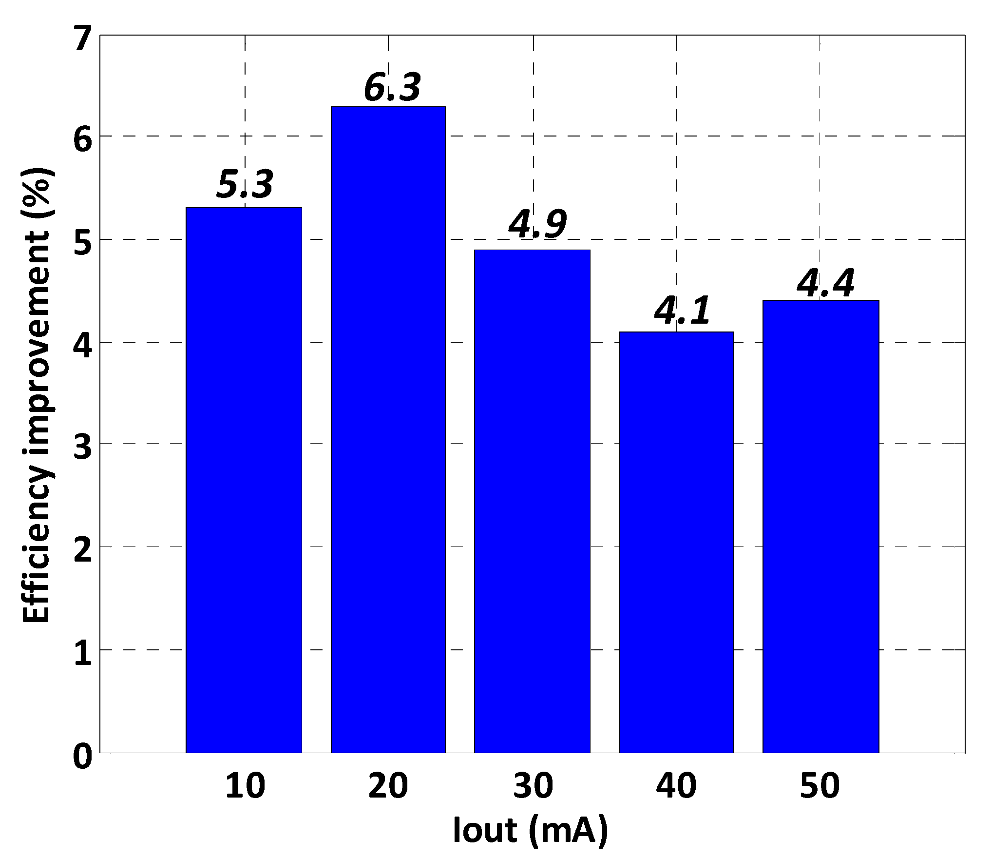
The efficiency improvement graph, shown in Figure 11, compares our proposed work with the latest state-of-the-art work [28]. This shows that our improvement in power efficiency ranges approximately from 4 to 6% across a 10~50 mA load current. Our proposed specification and performance are summarized in Table 1. It clearly shows that the proposed TFCS and ALCS technique yields an improvement in the power efficiency (4~6%) compared to some of the latest state-of-the-art research work [17,18,19]. However, one drawback is the fact that the external inductor and capacitor are relatively larger in our proposed work so as to achieve a smaller peak-to-peak output voltage ripple for a more accurate sensing of the load current. The measured line and load regulation for our proposed work are about 21 mV/V and 0.53 mV/mA, respectively. The output voltage recovery time subjected to a sudden load change from no load to full load is <20 µs.
4. Discussion and Conclusions
One area of improvement is to use the MOSFET segmentation technique proposed in [30,31,32], which can help to further improve the power conversion efficiency. At the same time, our proposed work is not optimized for deadtime control; hence, there is ongoing current research into designing a deadtime controller to minimize body diode conduction loss, which will improve efficiency. This ongoing work into deadtime control is a continuation of this proposed work. In addition, the simulation results for the power efficiency of our proposed work are about 2~3% better than our testing results. The rationale for this margin is due to the power loss in the resistance of the Au (Gold) wire bonding, the DIP package leads and the resistance in the traces of the PCB board. Careful consideration, recommended by [33], has been taken into account when designing the PCB board so that important power/ground lines have as short but as wide a trace as possible to minimize unnecessary power losses. Overall, our proposed TFCS and ALCS indeed yield an efficiency improvement over some of the latest research works, though with a relatively larger external inductor and filtering capacitor. At last, a buck DC-DC converter with the proposed TFCS and ALCS has been designed and implemented with 0.18 µm 1P6M CMOS technology, occupying an area of 1.3 mm2. It yields a peak efficiency of about 92.7% when the buck converter is operating at 250 kHz with a 2.0 V input voltage and a 1.25 V output voltage with a load current of 30 mA. The proposed buck converter is implemented and dedicated for smartphone application, whereby it spends most of its time under idle, low load conditions.
5. Future Work
One aspect of future work is to design and implement envelope tracking, which is important for smartphone applications, whereby it uses 3G/4G technology. For the proposed work in this thesis, it focuses more towards achieving higher power efficiency by optimizing body diode conduction, reverse inductor current and better delivery for a wide range of load currents. The next aspect of future work includes working on the circuit block of the battery charger, which comprises the detection mechanism for a low battery shelf life. Another aspect of future work will focus on the safety aspect of the DC-DC converter, which consists of over-current and over-voltage protection circuits. In addition, since the power transistors are drawing a huge amount of current and causes the overheating of the PCB board, thermal management has to be employed to ensure long-term reliability. This also includes employing on-chip temperature sensors to detect hot-spots during chip measurement. The final aspect of future work is to design on-chip LDO regulators, which can be used for silicon-on-chip (SoC) integration and yet be able to yield high PSR values at frequencies above 10 MHz.
Author Contributions
Conceptualization, C.L.K.; Supervision, L.S. All authors have read and agreed to the published version of the manuscript.
Funding
This research received no external funding.
Data Availability Statement
Data are contained within the article.
Acknowledgments
Our team would like to express our deepest gratitude to Global Foundries and the Singapore Economic Development Board (EDB) for supporting our research work.
Conflicts of Interest
The authors declare no conflict of interest.
Appendix A
Sensing the inductor current in a buck converter is an important function of the DC-DC controller. Its current-sensing circuit should be easy to implement without increasing the form factor. Furthermore, the current sensor has to be fast for a high-switching frequency DC-DC converter in order to reduce the inductor size. Past research works yielded many interesting current sensing techniques. One of them is to sense the on-resistance of the power transistor directly [34], but the drawback lies in the fact that the resistance value may change significantly by ±30% due to the PVT variation during the fabrication of the die. Hence, this technique is unreliable. Another work [35] instead proposed a novel self-learning technique to sense the instantaneous induct current via the parasitic resistance (DCR) of the inductor. One of the benefits include minimal power losses and thus makes it applicable to varying loading conditions. In addition, it completely eliminates unnecessary losses by not introducing any additional passive components in the power line. However, it requires a very complex circuit implementation, which occupies a large silicon area overhead. At the same time, the more widely used approach is based on the sensing of the current [36,37,38] that passes through the power transistor. It employs the use of matched current mirrors and a high gain amplifier to mirror a fraction of the current going through the respective power transistor to the sensing transistor. However, one of its disadvantages is that its accuracy is poor, as it depends heavily on the matching performance of the current mirror in the ohmic region. Furthermore, channel-length modulation and process mismatch will induce an error of >15% [39]. On the other hand, there is a proposed use of a current offset cancellation technique [40] to further improve the accuracy of current sensing. However, one of its minor drawbacks is the relatively larger quiescent current required to provide the driving capability, which leads to a degradation in the power efficiency. Hence, it suffers an imminent tradeoff between speed and accuracy. Some other techniques employ the advantage of the availability of a bipolar transistor in the BiCMOS process [41] to enhance the accuracy of its current sensing capability. This, however, proves to be too costly to implement. There is also a filter approach, which senses the current in a continuous mode [42] by applying an inductor voltage across a tuned low-pass filter and by sensing the filter current. One of its advantages is that it has minimal switching noise, but its inherent accuracy is highly dependent on the DCR of the inductor and the tuning accuracy of the filter, which may lead to a variation of >±20%. One of the more recent works [19] uses a tri-mode operation (PFM, PWM and DGM) to handle a 100,000× load range. It works on the fact that by reducing the comparator current, a delay-based hysteresis window adaptive to the load current is generated, thereby reducing the total switching power loss. However, this converter is implemented in 0.18 um BCD technology, which is too costly for us to handle, and the power efficiency seems to degrade drastically under very light load conditions (<100 µA). At the same time, there are other converters which are capable of providing a wide load range with good efficiency and consuming a very low quiescent current, which will no doubt be the major power consumption in sensing or low load mode [17,18,43,44,45,46,47,48].
However, in our proposed TFCS and ALCS DC-DC buck converter, it employs a very accurate ALCS circuit, which is an extension and improvement to the prior work [20]. It is able to achieve high accuracy in the current sensing at the tradeoff of a slightly higher quiescent power consumption and a larger inductor value so as to minimize the output voltage ripple, which will lead to inaccuracies in the sensing voltage, Vsense.
References
- Lee, W.; Wang, Y.; Shin, D.; Chang, N.; Pedram, M. Power conversion efficiency characterization and optimization for smartphones. In Proceedings of the ISLPED’12: International Symposium on Low Power Electronics and Design, Redondo Beach, CA, USA, 30 July–1 August 2012; pp. 103–108. [Google Scholar]
- Carrol, A.; Heiser, G. An Analysis of Power Consumption in a Smartphone. In Proceedings of the USENIX Annual Technical Conference, Boston, MA, USA, 22–25 June 2010; pp. 271–284. [Google Scholar]
- Huh, Y. Future direction of power management in mobile devices. In Proceedings of the 2011 IEEE Asian Solid-State Circuits Conference (A-SSCC), Jeju, Republic of Korea, 14–16 November 2011; pp. 1–4. [Google Scholar]
- Kim, H. Trends of R&D on Lithium Secondary Batteries for Electricial Vehicles. In Proceedings of the Smart Battery/Cell Forum, Seoul, Republic of Korea, 22 June 2011. [Google Scholar]
- Dong, M.; Zhong, L. Self-constructive high-rate system energy modeling for battery-powered mobile systems. In Proceedings of the MobiSys’11: The 9th International Conference on Mobile Systems, Applications, and Services, Bethesda, MD, USA, 28 June–1 July 2011; pp. 335–348. [Google Scholar]
- Lide, Z.; Tiwana, B.; Dick, R.P.; Zhiyun, Q.; Mao, Z.M.; Zhaoguang, W.; Lei, Y. Accurate online power estimation and automatic battery behavior based power model generation for smartphones. In Proceedings of the IEEE International Conference on Hardware/Software Codesign and System Synthesis, Scottsdale, AZ, USA, 24–29 October 2010; pp. 105–114. [Google Scholar]
- Ma, D.; Bondade, R. Enabling Power-Efficient DVFS Operations on Silicon. IEEE Circuits Syst. Mag. 2010, 10, 14–30. [Google Scholar] [CrossRef]
- Chester, S. Characteristics of Rechargeable Batteries; Appl. Rep. no. “SNVA533”; Texas Instruments: Dallas, TX, USA, 2011. [Google Scholar]
- Sahu, B.; Rincon-Mora, G. A high-efficiency, dual-mode, dynamic, buck-boost power supply IC for portable applications. In Proceedings of the 18th International Conference on VLSI Design, Kolkata, India, 3–7 January 2005; pp. 858–861. [Google Scholar]
- Instruments, T. Handset: Smartphone. Available online: http://www.ti.com/solution/handset_smartphone (accessed on 14 July 2023).
- Sahu, B.; Rincon-Mora, G.A. An Accurate, Low-Voltage, CMOS Switching Power Supply with Adaptive On-Time Pulse-Frequency Modulation (PFM) Control. IEEE Trans. Circuits Syst. I Regul. Pap. 2007, 54, 312–321. [Google Scholar] [CrossRef]
- Mulligan; Broach, B.; Lee, T. A constant-frequency method for improving light-load efficiency in synchronous buck converters. IEEE Power Electron. Lett. 2005, 3, 24–29. [Google Scholar] [CrossRef]
- Lee, H.; Ryu, S.-R. An Efficiency-Enhanced DCM Buck Regulator with Improved Switching Timing of Power Transistors. IEEE Trans. Circuits Syst. II Express Briefs 2010, 57, 238–242. [Google Scholar] [CrossRef]
- Sun, Z.; Siek, L. A novel ripple controlled modulation for high efficiency DC-DC converters. In Proceedings of the 2011 International Symposium on Integrated Circuits (ISIC), Singapore, 12–14 December 2011; pp. 238–241. [Google Scholar]
- Musunuri, S.; Chapman, P. Improvement of light-load efficiency using width-switching scheme for CMOS transistors. IEEE Power Electron. Lett. 2005, 3, 105–110. [Google Scholar] [CrossRef]
- Huang, H.-W.; Chen, K.-H.; Kuo, S.-Y. Dithering Skip Modulation, Width and Dead Time Controllers in Highly Efficient DC-DC Converters for System-On-Chip Applications. IEEE J. Solid-State Circuits 2007, 42, 2451–2465. [Google Scholar] [CrossRef]
- Park, Y.-J.; Park, J.-H.; Kim, H.-J.; Ryu, H.; Kim, S.; Pu, Y.; Hwang, K.C.; Yang, Y.; Lee, M.; Lee, K.-Y. A design of a 92.4% efficiency triple mode control DC–DC buck converter with low power retention mode and adaptive zero current detector for IoT/wearable applications. IEEE Trans. Power Electron. 2017, 32, 6946–6960. [Google Scholar] [CrossRef]
- Santoro, F.; Kuhn, R.; Gibson, N.; Rasera, N.; Tost, T.; Graeb, H.; Wicht, B.; Brederlow, R. A hysteretic buck converter with 92.1% maximum efficiency designed for ultra-low power and fast wake-up SoC applications. IEEE J. Solid-State Circuits 2018, 53, 1856–1868. [Google Scholar] [CrossRef]
- Zhao, M.; Li, M.; Song, S.; Hu, Y.; Yao, Y.; Bai, X.; Hu, R.; Wu, X.; Tan, Z. An Ultra-Low Quiescent Current Tri-Mode DC-DC Buck Converter with 92.1% Peak Efficiency for IoT Applications. IEEE Trans. Circuits Syst. I Regul. Pap. 2022, 69, 428–439. [Google Scholar] [CrossRef]
- Lam, Y.-H.; Ki, W.-H.; Tsui, C.-Y.; Ma, D. Integrated 0.9 V charge-control switching converter with self-biased current sensor. In Proceedings of the 2004 47th Midwest Symposium on Circuits and Systems, Hiroshima, Japan, 25–28 July 2004; pp. 305–308. [Google Scholar]
- Stratakos, A.; Sanders, S.; Brodersen, R. A low-voltage CMOS DC-DC converter for a portable battery-operated system. In Proceedings of the 1994 Power Electronics Specialist Conference—PESC’94, Taipei, Taiwan, 20–25 June 1994; pp. 619–626. [Google Scholar]
- Katayama, Y.; Edo, M.; Denta, T.; Kawashima, T.; Ninomiya, T. Optimum design method of CMOS IC for DC-DC converter that integrates power stage MOSFETs. In Proceedings of the 2004 IEEE 35th Annual Power Electronics Specialists Conference, Aachen, Germany, 20–25 June 2004; pp. 4486–4491. [Google Scholar]
- Chen, Y.; Fu, Y.; Cheng, X.; Wu, T.X.; Shen, Z.J. Modeling and Analysis of Metal Interconnect Resistance of Power IC’s. In Proceedings of the 19th International Symposium on Power Semiconductor Devices and IC’s, Jeju, Republic of Korea, 27–31 May 2007; pp. 253–256. [Google Scholar]
- Baker, L.; Currences, R.; Law, S.; Le, M.; Lee, C.; Lin, S.T.; Teene, M. A ‘waffle’ layout technique strengthens the ESD hardness of the NMOS output transistor. In Electrical Overstress/Electrostatic Discharge Symposium Proceedings; EOS/ESD Association, Inc.: Rome, NY, USA, 1989; pp. 175–181. [Google Scholar]
- Bosch, A.V.D.; Steyaert, M.; Sansen, W. A high density matched hexagonal transistor structure in standard CMOS technology for high speed applications. In Proceedings of the International Conference on Microelectronic Test Structures, Gothenburg, Sweden, 15–18 March 1999; pp. 212–215. [Google Scholar]
- Yoo, A.; Chang, M.; Trescases, O.; Ng, W.T. High Performance Low-Voltage Power MOSFETs with Hybrid Waffle Layout Structure in a 0.25 µm Standard CMOS Process. In Proceedings of the 2008 20th International Symposium on Power Semiconductor Devices and IC’s, Orlando, FL, USA, 18–22 May 2008; pp. 95–98. [Google Scholar]
- Yoo, A. Design, Implementation, Modeling, and Optimization of Next Generation Low-Voltage Power MOSFETs. Ph.D. Thesis, Department of Materials Science and Engineering, University of Toronto, Toronto, ON, Canada, 2010. [Google Scholar]
- Sun, Z.; Chew, K.W.R.; Tang, H.; Siek, L. Adaptive Gate Switching Control for Discontinuous Conduction Mode DC–DC Converter. IEEE Trans. Power Electron. 2014, 29, 1311–1320. [Google Scholar] [CrossRef]
- Kong, T.-H.; Woo, Y.-J.; Wang, S.-W.; Hong, S.-W.; Cho, G.-H. Zero-order control of boost DC-DC converter with transient enhancement using residual current. In Proceedings of the 2011 IEEE International Solid-State Circuits Conference, San Francisco, CA, USA, 20–24 February 2011; pp. 390–392. [Google Scholar]
- Man, T.Y.; Mok, P.K.T.; Chan, M.J. A 0.9-V Input Discontinuous-Conduction-Mode Boost Converter with CMOS-Control Rectifier. IEEE J. Solid-State Circuits 2008, 43, 2036–2046. [Google Scholar] [CrossRef]
- Yan, W.; Li, W.; Liu, R. A Noise-Shaped Buck DC–DC Converter with Improved Light-Load Efficiency and Fast Transient Response. IEEE Trans. Power Electron. 2011, 26, 3908–3924. [Google Scholar] [CrossRef]
- Trescases, O.; Wei, G.; Prodic, A.; Ng, W.T. Predictive Efficiency Optimization for DC–DC Converters with Highly Dynamic Digital Loads. IEEE Trans. Power Electron. 2008, 23, 1859–1869. [Google Scholar] [CrossRef]
- Wong, K. Parasitics Can Hinder Switching Regulator and LDO Designs; Appl. Rep. no. “SNVA689”; Texas Instruments: Dallas, TX, USA, 2013. [Google Scholar]
- Smith, T.; Dimitrijev, S.; Harrison, H. Controlling a DC-DC converter by using the power MOSFET as a voltage controlled resistor. IEEE Trans. Circuits Syst. I Regul. Pap. 2000, 47, 357–362. [Google Scholar] [CrossRef]
- Forghani-Zadeh, H.P.; Rincon-Mora, G.A. An Accurate, Continuous, and Lossless Self-Learning CMOS Current-Sensing Scheme for Inductor-Based DC-DC Converters. IEEE J. Solid-State Circuits 2007, 42, 665–679. [Google Scholar] [CrossRef]
- Leung, C.Y.; Mok, P.; Leung, K.N.; Chan, M. An integrated CMOS current-sensing circuit for low-Voltage current-mode buck regulator. IEEE Trans. Circuits Syst. II Analog. Digit. Signal Process. 2005, 52, 394–397. [Google Scholar] [CrossRef]
- Leung, C.Y.; Mok, P.K.T.; Leung, K.N. A 1-V integrated current-mode boost converter in standard 3.3/5-V CMOS technologies. IEEE J. Solid-State Circuits 2005, 40, 2265–2274. [Google Scholar] [CrossRef]
- Lee, C.F.; Mok, P. A monolithic current-mode CMOS DC–DC converter with on-chip current-sensing technique. IEEE J. Solid-State Circuits 2004, 39, 3–14. [Google Scholar] [CrossRef]
- Drennan, P.; McAndrew, C. Understanding MOSFET mismatch for analog design. IEEE J. Solid-State Circuits 2003, 38, 450–456. [Google Scholar] [CrossRef]
- Lam, H.; Ki, W.-H.; Ma, D. Loop gain analysis and development of high-speed high-accuracy current sensors for switching converters. In Proceedings of the 2004 IEEE International Symposium on Circuits and Systems, Vancouver, BC, Canada, 23–26 May 2004; pp. 828–831. [Google Scholar]
- Corsi, M. Current sensing schemes for use in BiCMOS integrated circuits. In Proceedings of the Bipolar/Bicmos Circuits and Technology Meeting, Minneapolis, MN, USA, 2–3 October 1995; pp. 55–57. [Google Scholar]
- Sassone, G.; Passoni, M.; Dallago, E. Lossless current sensing in low-voltage high-current DC/DC modular supplies. IEEE Trans. Ind. Electron. 2000, 47, 1249–1252. [Google Scholar] [CrossRef]
- Zhang, S.; Zhao, M.; Wu, X.; Zhang, H. Dual-phase DC–DC buck converter with light-load performance enhance-ment for portable applications. IET Power Electron. 2018, 11, 719–726. [Google Scholar] [CrossRef]
- Hong, W.; Lee, M. A 7.4-MHz tri-mode DC-DC buck converter with load current prediction scheme and seamless mode transition for IoT applications. IEEE Trans. Circuits Syst. I Regul. Pap. 2020, 67, 4544–4555. [Google Scholar] [CrossRef]
- Cheng, L.; Lai, X.; Shi, L. Low-quiescent-current flexible mode buck–boost converter. IET Power Electron. 2015, 8, 2520–2528. [Google Scholar] [CrossRef]
- Chen, P.-H.; Wu, C.-S.; Lin, K.-C. A 50 nW-to-10 mW output power tri-mode digital buck converter with self-tracking zero current detection for photovoltaic energy harvesting. IEEE J. Solid-State Circuits 2016, 51, 523–532. [Google Scholar]
- Zeng, W.-L.; Ren, Y.; Lam, C.-S.; Sin, S.-W.; Che, W.-K.; Ding, R.; Martins, R.P. A 470-nA quiescent current and 92.7%/94.7% efficiency DCT/PWM control buck converter with seamless mode selection for IoT application. IEEE Trans. Circuits Syst. I Regul. Pap. 2020, 67, 4085–4098. [Google Scholar] [CrossRef]
- Chen, P.-H.; Cheng, H.-C.; Ai, Y.-A.; Chung, W.-T. Automatic mode-selected energy harvesting interface with >80% power efficiency over 200 nW to 10 mW. IEEE Trans. Very Large Scale Integr. (VLSI) Syst. 2018, 26, 2898–2906. [Google Scholar] [CrossRef]
Figure 1.
A vital part of the 3G/4G smartphone power management unit (PMU).

Figure 2.
Proposed twin frequency control DC-DC buck converter using accurate load current sensing technique.
Figure 2.
Proposed twin frequency control DC-DC buck converter using accurate load current sensing technique.

Figure 3.
Accurate load current sensing (ALCS) block.

Figure 4.
Four-bit thermometer code ADC.

Figure 5.
Proposed twin frequency control scheme (TFCS).

Figure 6.
Optimized sizing of (a) NMOS power transistor; (b) PMOS power transistor.

Figure 7.
Die photo of the buck converter with proposed TFCS and ALCS.

Figure 8.
Prototype of a buck converter with proposed TFCS and ALCS.

Figure 9.
Peak efficiency achieved—waveform of Vx and Vint (VBATT = 2 V, Vout = 1.25 V, Freq = 250 kHz and Iload = 30 mA).
Figure 9.
Peak efficiency achieved—waveform of Vx and Vint (VBATT = 2 V, Vout = 1.25 V, Freq = 250 kHz and Iload = 30 mA).

Figure 10.
Power efficiency of the proposed TFCS and ALCS buck converter and the conventional PWM/PFM controller under different loading conditions (P—Proposed Work; C—Conventional Work).
Figure 10.
Power efficiency of the proposed TFCS and ALCS buck converter and the conventional PWM/PFM controller under different loading conditions (P—Proposed Work; C—Conventional Work).

Figure 11.
Efficiency improvement of the proposed TFCS and ALCS buck converter compared to the latest state-of-the-art work [28].
Figure 11.
Efficiency improvement of the proposed TFCS and ALCS buck converter compared to the latest state-of-the-art work [28].


Table 1.
Performance summary and comparison.
| Unit | TPEL [17] | JSSC [18] | TCAS I [19] | This Work | |
|---|---|---|---|---|---|
| Year | - | 2017 | 2018 | 2022 | 2023 |
| Technology | µm | 0.13 (CMOS) | 0.13 | 0.18 (BCD) | 0.18 (CMOS) |
| Input Voltage | V | 2.2~3.3 | 1.8~3.3 | 2.7~4.7 | 2.0~3.0 |
| Output Voltage | V | 1.7 | 1.2 | 1.6 | 1.25 |
| Peak Efficiency@Load Current | % | 90.4@10 mA | 84.0@100 µA | 92.1@10 mA | 92.7@30 mA |
| External Inductor | µH | 3.0 | 18 | 4.7 | 47.0 |
| External Capacitor | µF | 3.0 | 0.056 | 4.7 | 10.0 |
| Frequency | kHz | 2500 | 3000–5500 | 4000 | 250 |
| Chip Silicon Area | mm2 | 0.656 | 0.2576 | 0.55 | 1.3 |
| Power Transistors Implemented in This Work: | |||||
| Size | Unit | MN | MP | ||
| Finger Width | µm | 19.6 | - | 19.6 | - |
| No. of Fingers | - | 60 | - | 91 | - |
| Multiplier | - | 18 | - | 20 | - |
| Channel Resistance | mΩ | Ron,n | 80 | Ron,p | 95 |
| Bonding Wire Resistance 1 | mΩ | Rbond,n | 200 | Rbond,p | 200 |
| Total Resistance 2 | mΩ | Roverall,n | 280 | Roverall,p | 295 |
| Total Gate Capacitance 3 | pF | Cgn | 477.8 | Cgp | 574.3 |
1 Wire bonding performed using A*STAR IME—Au (Gold) Wire (1 mil diameter and 650 mA/cm). 2 Impedance and inductance for a bonding wire per unit cm are 1 Ω and 10 nH, respectively. 3 Post layout extraction, including bond pads (performed using Calibre). Other remarks: process has 6 metal layers (EMI: M1–M5 → 1 mA/µm, M6 → 5.34 mA/µm at 30 °C).
Table 2.
Transistor Sizing (W/L) Ratio.
| Transistor No | W/L Sizing |
|---|---|
| MP1 to MP4 | 4 µm/10 µm |
| MN1, MN2, MN3 | 2 µm/10 µm |
| MN4, MN5, MN7 | 1 µm/5 µm |
| MN6 | 1 µm/20 µm |
| MP5 to MP8 | 2 µm/10 µm |
Disclaimer/Publisher’s Note: The statements, opinions and data contained in all publications are solely those of the individual author(s) and contributor(s) and not of MDPI and/or the editor(s). MDPI and/or the editor(s) disclaim responsibility for any injury to people or property resulting from any ideas, methods, instructions or products referred to in the content. |
© 2023 by the authors. Licensee MDPI, Basel, Switzerland. This article is an open access article distributed under the terms and conditions of the Creative Commons Attribution (CC BY) license (https://creativecommons.org/licenses/by/4.0/).
Share and Cite
MDPI and ACS Style
Kok, C.L.; Siek, L. Designing a Twin Frequency Control DC-DC Buck Converter Using Accurate Load Current Sensing Technique. Electronics 2024, 13, 45. https://doi.org/10.3390/electronics13010045
AMA Style
Kok CL, Siek L. Designing a Twin Frequency Control DC-DC Buck Converter Using Accurate Load Current Sensing Technique. Electronics. 2024; 13(1):45. https://doi.org/10.3390/electronics13010045
Chicago/Turabian StyleKok, Chiang Liang, and Liter Siek. 2024. "Designing a Twin Frequency Control DC-DC Buck Converter Using Accurate Load Current Sensing Technique" Electronics 13, no. 1: 45. https://doi.org/10.3390/electronics13010045
Note that from the first issue of 2016, this journal uses article numbers instead of page numbers. See further details here.