
Circuit Models of Power MOSFETs Leading the Way of GaN HEMT Modelling—A Review


Department of Electrical Electronic and Computer Engineering, University of Catania, 95125 Catania, Italy
*
Author to whom correspondence should be addressed.
Energies 2022, 15(9), 3415; https://doi.org/10.3390/en15093415
Submission received: 2 March 2022
/
Revised: 22 April 2022
/
Accepted: 29 April 2022
/
Published: 7 May 2022
(This article belongs to the Section F3: Power Electronics)
Abstract
:Gallium nitride high-electron-mobility transistor (GaN HEMT) is a key enabling technology for obtaining high-efficient and compact power electronic systems. At the design stage of a power converter, the proper modelling of the GaN HEMT is essential to benefit from their good features and to account for the limits of the current technology. Circuit models of power MOSFETs have been deeply investigated by academia and industry for a long time. These models are able to emulate the datasheet information, and they are usually provided by device manufacturers as netlists that can be simulated in any kind of SPICE-like software. This paper firstly highlights the similarities and differences between MOSFETs and GaN HEMTs at the datasheet level. According to this analysis, the features of MOSFET circuit models that can be adopted for GaN HEMT modelling are discussed. This task has been accomplished by overviewing the literature on MOSFETs circuit models as well as analysing manufacturers netlists, thus highlighting the models MOSFETs valid or adaptable to GaN HEMTs. The study has revealed show that some models can be adapted for the GaN HEMT devices to emulate static characteristics at room temperature while the MOSFET models of dynamic characteristics can be used for GaN HEMT devices. This study enables the devices modellers to speed up the GaN HEMT modelling thanks to the use of some well-established MOSFET models. In this perspective, some suggestions to develop accurate GaN HEMT models are also provided.
1. Introduction
The worldwide growth of environmental awareness has pushed toward the diffusion of green power sources and high-efficiency power components and systems [1,2,3]. In such a contest, the devices based on wide-bandgap (WBG) materials, in particular, silicon carbide (SiC) [4,5] and gallium nitride (GaN) [6,7], have a key role in developing high-efficiency converters. GaN high-electron-mobility transistors (HEMTs) also enable the design of highly compact power converters [8], which are very attractive in many industrial and commercial sectors [9]. More specifically, the encumbrance and weight lowering are achieved thanks to the reduction in the device size in comparison with previous technologies and, above all, thanks to the reduction in the size of passive components which is due to the ability at operating at a higher switching frequency [10,11]. Figure 1 shows the application areas of the three different device technologies. SiC devices are a candidate in substituting Si IGBT devices in applications such as traction inverters and industrial manufacturing sectors [12], while GaN devices are better than Si MOSFETs for the on-board converters and switch-mode power supply used in data centres and IoT applications [13].
The design stage of converters including GaN HEMTs is very critical due to the combination of their fast switching with the parasitic inductances of the packaging and board [14,15,16] that, in turn, interact with the parasitic capacitances of the device as well [17]. Overvoltages and oscillations are some of the main related phenomena that could lead to many issues, e.g., exceeding the device breakdown voltage, electromagnetic interference, multiple false device trigger and so on [18,19,20]. These issues can be partially faced by innovative driving techniques [21] provided that an optimal design of the converter is performed.
The computer-aided design (CAD) of a GaN-based power converter needs an accurate model of the device to foresee, by means of simulations, the efficiency and waveforms related to different design choices [22,23]. The use of enhanced models for the evaluation of efficiency is a common practice in many sectors [24,25].
The first modelling approaches date back to the 1970s with technology CAD (TCAD) software [26]. In this case, the model accounts for the device physics, and the modelling can support the device development, that is, the design of the device only (computer-aided manufacturing). On the other hand, these models can be useful at the converter design stage, since the knowledge of the physical relationships that govern the device, embedded into the converter, enable them to accurately foresee its behaviour [27]. However, when these device models are used for converter design, the simulation time could be unacceptable in the industrial sector [28]. Another problem is that device models themselves could require a great development effort and time. Moreover, they require information about the technology which is not available to the users. Hence, only the manufacturers can develop this kind of model. In this case, probably, the model is provided as a black box (since manufacturers usually do not want to provide technology information) developed for simulation in specific tools.
Behavioural models consist of a set of equations that do have not any relation to the device physics [29]. The parameters of the equations are set to emulate the device behaviour at the terminals, and they can be easily implemented in SPICE-like simulation tools, largely adopted both in industrial and academic contexts [30,31]. This black-box approach can be used also in the modelling of power converters [32]. The major issue of the behavioural model is the identification of the value of the parameters to obtain simulations results that fit with measurements [33]. To perform this task, the use of stochastic optimization algorithms is the best way to find the optimal value of the fitting parameters, that is, the value involving a better approximation of the actual waveforms [34]. Finally, semi-physical models are behavioural models partially based on device physics. Semi-physical and behavioural models, referred to as “circuit models” in the following, are only considered in this paper.
The target of circuit modelling is fitting quantities and waveforms obtained by simulation with the datasheet and laboratory measurements. In other words, the model must emulate the device behaviour in static and dynamic conditions. In this perspective, the circuit model must be accurate to properly support the design stage. On the other hand, as said before, the time necessary for the development of the model and the computational effort the model requires during a simulation are important aspects to be considered. The development of models of new devices must consider these crucial aspects. Therefore, if a new device presents some features similar to those of another well-established device satisfying these conflicting targets, the new device can be modelled readapting the approach used in the (good) model of the latter to account for these features.
In this context, the main contribution of the paper is the analysis of the literature related to MOSFET models as well as the analysis of manufactures netlists that have been performed to highlight the features of MOSFET models that can be adopted for GaN HEMT modelling. The study has revealed that some models can be adapted for the GaN HEMT devices to emulate the static characteristics at room temperature, while the MOSFET models of dynamic characteristics can be used for GaN HEMT devices. This study enables the devices modellers to speed up the GaN HEMT modelling, thanks to the use of some well-established MOSFET models.
With this in mind, in Section 2, the main similarities and differences between power MOSFETs and GaN HEMT datasheets are analysed. The results of this comparison are combined, in Section 3, with an overview of power MOSFETs modelling approaches to highlight the ones that can be useful to develop circuit models of GaN HEMTs. Finally, the conclusion of the study has been reported.
2. Comparison between MOSFET and GaN HEMT
This section analyses the main similarities and differences between MOSFET (Si and SiC technologies) and GaN HEMT devices. The results of the comparison aim at highlighting the modelling approaches that can be transferred to GaN HEMTs. The comparison considers datasheet information and, more in general, the common data used to build circuit models of MOSFETs. More specifically the pieces of information usually considered for MOSFET modelling are:
- Output characteristic;
- Transfer characteristic;
- Threshold voltage;
- Conduction resistance;
- Third quadrant and reverse recovery current;
- Parasitic capacitances.
In the following, various datasheets of Si MOSFET, SiC and GaN HEMT devices from different manufacturers have been considered for each point in the previous list, since the curves for a given technology and analogous breakdown voltage are similar regardless of the product family or manufacturer.
The devices analysed have breakdown voltages of 600 V or 650 V. Most of the analyses focus on GaN HEMTs with 650 V breakdown, though many basic considerations apply to 100 V GaN HEMT characteristics as well.
The following sub-section shows some comparisons among the three technologies: Si MOSFETs, SiC MOSFETs and GaN HEMTs. For each comparison, different devices are chosen to confirm the similarity among the devices of the same technology.
Therefore, for all these devices, the same circuit modelling strategy can be adopted to emulate the characteristic (e.g., the same formula could be adopted).
2.1. Output Characteristic
The output characteristic is one of the most important features of any device. It reports the drain current (ID) vs. the drain-source voltage (VDS). Various curves at different gate-source voltages, at room temperature, are typically reported (see Figure 2a,c,e). The output characteristic is also evaluated at a different temperature above the room temperature. Typical values are 125 °C or 150 °C for Si MOSFETs and GaN HEMTs and 175 °C for SiC MOSFET only (see Figure 2b,d,f). The recommended range of gate-source voltage (VGS) is usually between 4 V and 15 V for Si MOSFET, between 6 V and 20 V for SiC MOSFET, and between 2 V and 6 V for GaN HEMT.
In the MOSFET characteristics, three different regions are identified: the cut-off, the linear-ohmic and the saturation region. The cut-off region is situated at the bottom of the output characteristic. In this region, devices are considered open switches. The linear-ohmic region concerns the low VDS values with increasing current. The almost-flat zones are those where the MOSFET operates in the saturation region. The trend of the curves in the output characteristic of GaN HEMTs is similar to the MOSFET one. Figure 2 also highlights the dependence of the drain current on the temperature.
Considering Si and SiC MOSFET curves, when the temperature increases, the drain current increases for VGS values up to approximately 6 V for Si MOSFETs (12 V for SiC MOSFETs), and it decreases for higher VGS values. Instead, in GaN HEMT devices, as the temperature increases, the drain current decreases for any VGS. The temperature behaviour just described is highlighted in Section 2.2.
2.2. Transfer Characteristic
The transfer characteristic relates the drain current to the gate-source voltage (VGS). This characteristic is usually evaluated at different temperatures. The typical range of gate-source voltage (VGS) is usually between 0 V and 20 ÷ 25 V for Si and SiC MOSFET, while it is between 0 V and 5 V for GaN HEMT. Figure 3 shows typical curves of the transfer characteristic.
Figure 3 confirms the aforementioned variation of the drain current as the temperature increases at the various VGS shown in Figure 2. More specifically, the intersection between the curves in Figure 3a (Si MOSFET) and Figure 3b (SiC MOSFET) confirms that, at low VGS, the drain current increases as the temperature increases, while at high VGS, the drain current decrease as the temperature increases. The intersection point in Figure 3a,b is called zero temperature coefficient (ZTC). It corresponds to a gate voltage at which the device’s DC electrical performance remains constant with temperature. The temperature coefficient defined as ΔID/ΔTJ is positive below ZTC since the drain current increases as the temperature increases. While it is negative above ZTC, [41]. For VGS values below the ZTC point, the device could suffer from thermal problems because the local hot spots lead to more current, and due to this phenomenon, local power dissipation rises that, in turn, increases the current, and a possible thermal runaway situation can occur. The lack of such an intersection in Figure 3c confirms that this phenomenon is absent in GaN HEMT devices, since the drain current always decreases as the temperature increases.
2.3. Threshold Voltage Characteristic
The threshold voltage (VTH or VGS,TH) is the minimum voltage to apply between the gate and source pin to create the conductive channel and start flowing current in the device [42]. The threshold voltage characteristic relates the VTH to the temperature variation. This characteristic is very important because it affects the static characteristics (as output and transfer characteristics) when the device is simulated at a temperature different from the ambient one. The decrease in VTH causes an early switch-on of the device. This behaviour can be seen at the bottom of Figure 3a,b because the current starts to flow at a lower voltage VGS than the ambient temperature. The VTH characteristic, for specified values of drain current and drain-source voltage, is commonly given in the datasheets, in the range from −50 °C to approximately 175 °C. For both Si and SiC MOSFETs, it decreases when the temperature increases; therefore, it has a negative temperature coefficient [43] (see Figure 4).
Instead, in GaN HEMTs, since they have a different physical structure, the threshold voltage is almost temperature-independent, and usually, the VTH-temperature curve is not shown in the device datasheets.
Figure 5 shows the threshold voltage vs. temperature in a GaN HEMT cascode device. In this case, the VTH variation is due to the low-voltage Si MOSFET embedded in the cascode with a GaN depletion mode device.
2.4. Static On-Resistance (RDS,on) Characteristic
The static on-resistance, RDS,on, is the drain-source resistance at a specified drain current and gate-source voltage in the linear-ohmic region of the output characteristic. The on-resistance characteristic is evaluated when temperature varies in the range approximately from −50 °C to 175 °C for Si and SiC MOSFETs, while between −50 °C and 150 °C for GaN HEMT. The on-resistance of the device is usually normalized to its value at 25 °C. This characteristic is useful to foresee the device conduction losses and is one of the most important in the evaluation of power efficiency. Figure 6 shows typical trends for Si, SiC MOSFET, and GaN HEMT Si MOSFET and GaN HEMT present an increasing on-resistance with increasing temperature (positive temperature coefficient), while in SiC MOSFET, RDS,on has a negative temperature coefficient (the on-resistance decreases as temperature increases) below 25 °C. On the other hand, above room temperature, the on-resistance increases, thus obtaining a typical U-shape characteristic. As shown in Figure 6, the trend of the 3 curves is similar to the room temperature.
2.5. Third Quadrant and Reverse Recovery Current Characteristics
Third quadrant datasheets (Figure 7) refer to the device reverse conduction: negative drain current ID vs. negative drain-source voltage VDS. Curves for different gate-source voltage VGS at T = 25 °C are given, in the typical range of drain-source voltage (VDS) between −1 V and 0 V for Si MOSFET, and between −7 V and 0 V for SiC MOSFET and GaN HEMT. A MOSFET has an intrinsic body diode in its structure. This parasitic diode enables the third quadrant conduction, but it introduces the well-known problem of the reverse recovery current, which leads to much higher switching losses. Indeed, the value of also affects the third quadrant conduction, since it can reduce the voltage drop due to the current flowing into the channel. As shown in Figure 7a, at high VGS, the current flows simultaneously in the MOSFET channel and the diode, but when the VGS voltage becomes close to a negative value, the current starts to flow in the diode only [49]. As shown in Figure 7b, for a given current, the negative source-drain voltage drop increases as VGS decreases. Finally, when VGS becomes negative causes a change in the knee and the slope of curves (see Figure 7b).
GaN HEMT has not an intrinsic body diode. When it operates in third quadrant conduction the current flows into the 2DEG channel and it is affected by VGS [53,54]. For high VGS (higher than VTH), the first and third quadrants have similar curves. When VGS decreases, towards negative values, the current curve has the characteristic shape of a diode (see Figure 7c). The lack of a parasitic body diode avoids the presence of the reverse-recovery current phenomenon. On the other hand, in GaN HEMT cascode devices, the presence of the low-voltage Si MOSFET causes the reverse recovery current.
2.6. Capacitance Characteristic
The capacitance characteristic shows the relationship between the capacitances and the drain-source voltage across the device. These capacitances evaluated in the MOSFET and GaN HEMT devices are CISS (input small-signal capacitance), CRSS (reverse small-signal capacitance) and COSS (output small-signal capacitance). The equations of parasitic capacitances are shown in the following:
They are non-linear and “small signal” capacitances that influence the dynamic behaviour of a device. These capacitances are provided in the datasheet as curves depending on VDS in the range 0 ÷ 500 V (see Figure 8). The capacitances also depend on the size of the device, the capacitance values of the MOSFETs are about double those of the GaN HEMTs with the same VDS. The Si MOSFET based on Super-Junction technology presents a constant CISS and a strong variation of COSS and CRSS, at low VDS. A similar trend occurs in SiC MOSFETs, although the capacitance values, as well as their sweep, are less than in Si MOSFETs. Analogous considerations can be applied, in turn, to GaN HEMT, even if it presents lower capacitance values and lower capacitance sweep. In conclusion, although the capacitance values are different among the three technologies, the trend is quite similar.
Figure 9 shows the capacitances of the GaN HEMT cascode device and shows that, compared to other GaN HEMT devices, they have higher values due to the embedded Si MOSFET.
3. Circuit Model
Circuit models are widely used in academia and industry to design power converters and foresee their performance. The models use mathematical expressions to emulate the behaviour of the device. Some circuit models do not present any relation with the device physics (behavioural models), others include some device physical parameters in the mathematical expressions (semi-physics and physics models). Behavioural models use mathematical expressions whose fitting parameters (i.e., coefficients, exponents and so on) are appropriately set to emulate the datasheet quantities described in Section 2. Semi-physics models use physics quantities related to the device in combination with the aforesaid parameters. Finally, physics models adopt only equations and quantities strictly related to device physics. Behavioural and semi-physics models are quite accurate and enable fast simulations and development times. These two important features make them the most diffused ones. Therefore, only these kinds of the model are analysed in the following, and thus the considered circuit models are behavioural or semi-physics ones. Furthermore, in the semi-physical models of MOSFETs when they are adapted to GaN HEMTs, the semi-physical parameters become fitting parameters for GaN HEMTs. This is because the physical structure between MOSFET and GaN HEMT is different, so there is no correspondence for the semi-physical parameters. Any circuit model includes various blocks to emulate the static and dynamic behaviour of a device. Figure 10 shows the different blocks usually present in the circuit models of MOSFETs (Figure 10a,b) and GaN HEMTs (Figure 10c,d).
The GMOS block enables us to emulate the output and transfer characteristics that represent the static behaviour of the device. In the MOSFET model, block Vth emulates the dependence of the voltage threshold from the temperature, and it is used in combination with the GMOS block. When RVAR is considered (Figure 10a,c), it usually emulates the variation of the conduction resistance with the temperature, and it also affects the static behaviour of the model. Another static characteristic, the third quadrant curves related to the parasitic diode conduction, is emulated by the body diode and GMOS blocks in MOSFET, and a similar block is employed in GaN HEMT. Moreover, in the MOSFET, the reverse recovery diode block emulates the reverse recovery current of this parasitic diode, thus affecting the dynamic behaviour of the device.
In the same way, the blocks CGD (gate-drain capacitance), CDS (drain-source capacitance) and CGS (gate-source capacitance) model the capacitance characteristics both in MOSFET and GaN HEMT devices, thus enabling to account for the dynamic behaviour, such as the gate charge and the switching waveforms.
Finally, as mentioned in Section 2, the Vth and the reverse recovery diode blocks, existing only in the MOSFET model, must be considered in the cascade GaN HEMTs.
Many approaches can be used to implement each block. Therefore, in the following, these approaches are analysed to highlight those useful for the GaN HEMT modelling, taking into account the comparison reported in Section 2. For each block, the equations proposed in the literature (the papers have been collected by Scopus) and the ones developed by some semiconductor manufacturers are reported [58].
In the following equations, physical quantities are explained the first time they appear. Moreover, all quantities are listed in Abbreviation.
3.1. GMOS
The GMOS block is implemented through a controlled current source that sets the drain current of the device in the first-quadrant operation, by implementing non-linear equations that impose the shape of the drain current. These equations include some parameters whose value must be determined appropriately to fit the simulation curves that emulate the output and transfer characteristics.
As said in the introduction of this section, some models include physical quantities in the equations and are identified as semi-physics models. Among the best known for the GMOS block are the Shichman–Hodges model, the Enz–Krummenacher–Vittoz (EKV) model, the Angelov model and the Curtice–Etterberg model, which are discussed in the following.
In 1968, the Shichman–Hodges equation was developed [59,60]. This MOSFET model is usually known as MOSFET LEVEL 1 [61], which includes the channel length modulation:
where is the transconductance coefficient, W is the channel width, L is the channel length, VTH is the threshold voltage (see Section 3.2) and λ is the channel length modulation coefficient. The equation is implemented into a current source that emulates the three operational regions (cut-off, linear and saturation) by the three distinct equations that appear in Equation (2). In [61], Equation (2) is used for modelling the output characteristic of GaN HEMT.
MOSFET LEVEL 3 is a more complex model that describes the MOSFET behaviour more accurately than the standard MOSFET LEVEL 1 [62]:
where is the mobility modulation constant, Rs is the source resistance, Rd is the drain resistance, is the surface potential in strong inversion, is the body-effect parameter. Furthermore, these equations are adaptable to GaN HEMT device models as proved in the following. These equations have been used to emulate the behaviour of two GaN HEMTs devices developed by GaNSystem (GS66504B and GS66506T).
In Figure 11, the simulation results obtained by using the parameters values of the MOSFET LEVEL 3, in [62], are almost good. The comparison highlights a discrete ability of the MOSFET LEVEL 3 to be used for the behavioural models of GaN HEMT devices.
Some quantities depend on the temperature, but such dependence is not accounted for in the previous models. For this reason, in [58], a new model that accounts for the dependence of the current ID on the temperature variation has been proposed. Indeed, the model is based on MOSFET LEVEL 1:
where two temperature-dependent coefficients Vlin and KPsat are added to improve Equation (2); Vlin values are tabled, while KPsat is expressed as functions of the junction temperature Tj:
where KPsat0 and Ksat are fitting parameters.
At room temperature, the accuracy increases with increasing VGS. High accuracy is achieved at high temperatures for all VGS [65].
Another ID-temperature dependence of Equation (2) (MOSFET LEVEL 1) has been created in [66]:
where
and
where A-I are fitting parameters. In [66], W and L have been set equal to 1. When these fitting parameters are added, the model is not semi-physical but becomes behaviour. Excellent results are achieved both at room temperature and varying temperatures.
The need for temperature-dependent models is not the only necessity. Another request is to have a unique equation concerning the Shichman–Hodges model. In [67], the three operation regions can be described utilizing a single equation (based on the Shichman–Hodges equation):
where n and α are fitting parameters, that modify the transition between the linear and saturation region. At low VDS the hyperbolic tangent function looks like a linear function, thus emulating the linear-ohmic region. At high VDS, the hyperbolic tangent tends to be one; thus, the drain current depends only on the first term.
As early as 1995, there was a need for models with a single equation dependent on temperature. Indeed, the EKV model is based on two logarithmic functions. The original EKV model [68] is reported in the following equation:
where ϕt is the thermal voltage.
The aim of high accuracy has led to various models based on the EKV one. As in [69], the resulting model includes curve-fitting parameters to match the static characteristics and the effect of channel length modulation in the saturation region:
where kS is the sub-threshold slope, n and α are fitting parameters for the linear region. Equation (8) is valid for both first and third quadrant conduction currents and it is implemented with two opposite current sources in the GMOS block. The model accuracy increases when VGS increases. In [69], simulations carried out at different temperatures are reported and they are very accurate.
The Angelov model and Curtice–Etterberg models were developed for GaAs HEMT devices between the 1980s and 1990s. Since then, these models have been used for MOSFET devices. The Angelov model proposed a hyperbolic tangent function for emulating the static behaviour of the device [70].
where is the saturation voltage parameter and the argument is:
where Vpk is the value of VGS at which the transconductance reaches its maximum value. In [71,72], the Angelov model has been implemented in the MOSFET device. However, as this model does not emulate the temperature behaviour of the device, Equation (10) has been implemented to include temperature dependence.
where T25 is the room temperature, XT is a generic parameter temperature-dependent. Moreover, to improve the accuracy of the model, some parameters vary with VGS: , and .
The demand for ever more accurate models has led to the creation of new complex equations, based on the Angelov model. The one, proposed in [73], aims at improving the model in the High Voltage High Current region:
where
and
In the previous equations, A, B, C1, C2, C3, D, E, F, G1, G2, H1, H2, J, K, L, and M are fitting parameters. The presence of many fitting parameters allows the high level of accuracy of the model, but the evaluation of their optimal value is complicated and time-consuming. Hence, the use of an automatic tool for the optimal setting of these parameters is recommended [34].
Instead, the equation of the original Curtice–Etterberg FET model [74] is reported in the following:
where
where is a fitting parameter that allows the modify the output curves in the ohmic region, β is the fitting parameter for pinch-off, is the output voltage at which A0, A1, A2 and A3 are evaluated, and τ is the internal time delay of FET.
In [75], a model based on the Curtice one for SiC MOSFET:
where λ, λ’, VT, a and b are fitting parameters.
Another model based on the Curtice–Etterberg FET model is reported in [76], where accurate characteristics are obtained over a wide temperature range by using the following new equation, depending on VDS and VGS:
where
In the previous equations, C, kd, Bt, B0, H0, αB, αH, αA1, αA2, αk1, αk2, Ag0 and kg0 are fitting parameters and VDS,tr is the VDS voltage at which the transfer is measured in the datasheet. In Equation (14), a product of three terms appears. The first term is inspired by the model of the C3M device developed by Cree [58]. The second and third terms are based on the Curtice–Etterberg model. In the original Curtice–Etterberg model, the temperature dependence is not present, but this model includes temperature dependence using the two second-degree polynomial functions Ag and kg. In [76], the validation of the model has been carried out for different SiC MOSFETs from various manufacturers at different temperatures (25 °C and 150 °C), and the results are very accurate for all tested devices.
In [58], another temperature-dependent model based on the Curtice–Etterberg model is proposed. The GMOS equation proposed:
where , , a, b, c, d are fitting parameters, and are temperature-dependent fitting parameters. The model accuracy improves with increasing VGS [65].
Moreover, a new GMOS equation based on EKV and Curtice-Ettenberg model is proposed in [58].
where
where B1, B2, C1, CT, G1, gt, g1, g2 and g3 are fitting parameters. The results at 25 °C and 125 °C show that the model accuracy increases when the gate-source voltage decreases [65].
In more recent years, the need for behavioural models has arisen. This is in order not to have a dependence on the physical parameters of the device and for curves that can be modified in all their parts. The simplest behavioural models to emulate the output characteristic as in [77]:
where K1, K2, C0 and b are parameters to be optimally set to emulate the characteristic accurately. This equation allows the simulation of the linear-ohmic and saturation regions. The results show an excellent accuracy of the output characteristic at low VDS while the accuracy tends to decrease at high VDS values.
Another behavioural temperature-independent model is proposed in [78]:
where AC, SS, B, C, D and TH are fitting parameters. Equation (18) is used for modelling GaN HEMT in [79]. In Figure 12, the output and transfer characteristics simulated with Equation (18) in a SiC MOSFET and a GaN HEMT are reported. Figure 12 highlights that Equation (18) can be valid for the GaN HEMT model with almost excellent results.
The need for a temperature-dependent equation, earlier pointed out, is satisfied in [80]. The modelling approach considers the product of two mathematical equations. One equation account for the output characteristic while the other is for the transfer one. The final equation (Equation (19)) is implemented into the GMOS block:
where
The hyperbolic tangent function is used to fit the transfer characteristic. In the equation, k, a, b, c, and d are fitting parameters. While p and q are fitting parameters, but they are of the output characteristic function. VGS and VDS values are obtained using a quadratic function of temperature where is the junction temperature, and m1, m2, m3, m4, n1, n2, n3 and n4 are the fitting parameters.
The temperature dependence can also be implemented by means of an auxiliary current source placed in parallel with a current source, that models the drain current at 25 °C. Then, the GMOS block of Figure 10 is made of two current sources in parallel [81], and the current vs. temperature dependence is emulated by the following equation:
where IGMOS,25 is the drain current at 25 °C emulated by the other current source, and TCI1 and TCI12 are fitting parameters. To emulate the behaviour of the SiC MOSFET current as the temperature increases, TCI1 must assume a positive value and TCI2 must be less than TCI1.
Another similar approach is proposed in [82]. In this case, the drain current at room temperature is multiplied by a different factor that depends on the temperature.
where K is a negative fitting parameter.
Equations (20) and (21) can be used only when the models consider the range of VGS below ZTC. Nevertheless, these equations can be used for GaN HEMT. In Equation (20), TCI1 must be set at a negative value and TCI2 < TCI1. Instead, in Equation (21), K must have a positive value.
In conclusion, the GMOS block mainly accounts for the output and transfer characteristics, and as mentioned above (Section 2.1 and Section 2.2), the shape of these characteristics is quite similar for the three technologies. Therefore, the temperature-independent equations proposed for the GMOS in the circuit models of MOSFETs are valid also for GaN HEMTs by properly setting the parameters of the equation. The semi-physics models are suitable for GaN HEMT devices too. The same physical parameters used in the MOSFET model are used as fitting parameters in GaN HEMT [62]. However, when the temperature increases, the behaviour of the drain current in MOSFET and GaN HEMT is different. In GaN HEMT the drain current decreases with increasing temperature regardless of the value of VGS, while MOSFETs present this behaviour only at high VGS values. Hence, the temperature-dependent equations used for the GMOS of the MOSFETs must be adapted for GaN HEMTs. Instead, in Equations (20) and (21), it is sufficient to change the coefficients to emulate the variation of the current as the temperature varies in the GaN HEMT. Despite that, it is possible to simplify the equations for GaN HEMT, since its temperature behaviour does not depend on VGS values.
3.2. Vth-Threshold Voltage
This block implements the threshold voltage Vth variation with increasing temperature. The threshold voltage variation is very important because it affects the output and transfer characteristic: the term Vth is included in several equations of the GMOS block in Section 3.1.
In [82], the threshold voltage variation with temperature is modelled as a linear law:
where is a fitting parameter. This simple implementation allows fast simulation but at the cost of inaccurate results.
Another linear equation is proposed in [83]:
where VTH,25 is the threshold voltage at 25 °C, and is a fitting parameter. The results show that this equation provides a good fitting between the datasheet and target curves.
Better accuracy is achieved by implementing a third-degree polynomial function [81]:
where VT3, VT2 and VT1 are fitting parameters.
Nevertheless, the threshold voltage of GaN HEMT devices is temperature independent, therefore the previous equations implemented for MOSFETs are useless for GaN HEMT devices. However, in the case of GaN HEMT cascode devices, the equations implemented in the MOSFET for modelling the VTH variation with the temperature can be used.
3.3. RVAR
This block allows emulating the RDS,on (see Section 2.4) variation with the temperature. It is not always present in circuit models (see Figure 10). When it is used, it could interact with the GMOS block and, consequently, both of them could concur in emulating the output and transfer characteristics.
The RVAR block of Figure 10 can be implemented either with a current-controlled voltage source (CCVS) or with a voltage-controlled current source (VCCS).
The typical trend of the RDS,on vs. temperature curve, observed in SiC MOSFET between −50 °C and 175 °C (see Figure 6b), is called “U-shape”.
This trend can be perfectly reproduced by a second-degree polynomial function as the following [81]:
where is the typical RDS,on value at 25 °C, and TC1 and TC2 are fitting parameters.
Another second-degree polynomial equation, in this case implemented in a VCCS, is analysed in [58]:
where A1, A2 and A3 are fitting parameters.
Other implementations of the RVAR block also include the dependence on electrical variables in addition to the temperature dependence. As in [47,83] with the following equation:
where RD0, RD1, V1, V2, r, r0 and r1 are fitting parameters.
Additionally, in [58], the following exponential equation, implemented in a CCVS, is analysed:
where D1, D2, d1, d2, d3 and k are fitting parameters, while ID is the drain current. Equations (24) and (25) allow us to achieve satisfactory results but with a higher mathematical complexity [65]. If only the operating temperature range between 25 °C and 175 °C is considered to model the RVAR block for the SiC MOSFET, equations can be simplified, because in this temperature range, the trend of the curve is an increasing monotone function. For example, in [84], the following equation is proposed:
where kr is a fitting parameter.
This approach is useful for modelling the same block for the GaN HEMTs since a monotonous increase in RDS,on with increasing temperature is observed (see Figure 6c).
Some circuit models are able to account for RDS,on temperature curve without using the RVAR block (as in Figure 10b,d). In this case, the curve emulation is obtained through the GMOS equation [72]. The polynomial equations, developed for the GMOS block, consider the variation of on-state resistance with temperature.
In conclusion, the previous equations have been developed to reproduce the “U-shape” curve of SiC MOSFET in a temperature range between −50 °C and 175 °C. As highlighted in Section 2.4, the on-resistance curve above 25 °C is similar for the Si, SiC MOSFETs and GaN HEMT. Therefore, the RVAR equations for SiC MOSFET can be used for Si MOSFET and GaN HEMT only in a temperature range between 25 °C and 175 °C. However, Equation (29) can be used for the GaN HEMT in the temperature range between −50 °C and 150 °C because it is an increasing monotone function.
3.4. Third Quadrant Conduction
The third quadrant characteristic is enabled when the VDS, across the device, is negative. As explained in Section 2.5, the third quadrant current is simulated at negative and positive VGS. In several cases, the GMOS and body diode blocks cooperate to emulate the current in the third quadrant.
A first implementation of the body diode block in the MOSFET model could be achieved by means of the Shockley diode equation [85]:
where VDiode is the voltage across the diode, and Isb and ktb are fitting parameters. The previous equation has been tested for a MOSFET device and a GaN HEMT. The simulations are shown in Figure 13.
The results, shown in Figure 13, confirm that the models used for the MOSFET devices are adaptable to the GaN HEMT models with almost satisfying results.
However, the lack of dependence on the temperature is the main limit of this equation. To overcome this limitation a new equation has been proposed equation in [66]:
where IS,25 is the saturation current at 25 °C, q is the electron charge, k is the Boltzmann’s constant. This equation is implemented in the body diode block, which is placed in parallel with the CDS block, and they are in series with the diode resistance (see Figure 14a).
To improve the accuracy of the temperature-dependent models, in [80], the resistance of the diode is also modelled:
where
and N is the emission coefficient, Is the saturation current, Rdiode is the parasitic resistance of the diode, Rdiode,25 is the parasitic resistance of the diode at 25 °C, VEG is the bandgap voltage, XTI is a fitting parameter temperature-dependent, TRS1 and TRS2 are fitting parameters temperature independent. The model provides accurate results at −40 °C, 25 °C and 150 °C.
In recent years, the need has arisen to have behavioural models of the body diode. These models are temperature dependent, and they include the resistance of the diode too. In the following, these models are reported in order of complexity of their equations.
The body diode behavioural temperature-dependent model can be obtained also employing two voltage-controlled current sources (VCCS) that represent the diode resistance and diode current behaviours, as G2 and G3 in Figure 14b. In [58], the following equations are given for the two VCCSs (see Figure 14b):
where a1, a2 and B1 are fitting parameters and:
and A, B2, C and D are fitting parameters. The results show that the model is very accurate at negative VGS [65], if used together with a model of the GMOS block that also includes the third quadrant static characteristic of the drain-source current.
Another behavioural model with the equation for both the resistance of the body diode and the body diode is the following reported in [58]:
where a–c are temperature-dependent fitting parameters and:
and fkbb and fkaa are functions of the gate-source voltage and temperature. VSD is the source-drain voltage. With this model, good results are achieved for all VGS values [65].
The block of the body diode is always in parallel to the block of the CDS capacitance (see Figure 10), for this reason, it might be more effective to have a single block for both the body diode and CDS as in [58]:
where A1, A2, A3, B1, B2, B3, a1, b1, b2, b3, b4, c1, c2 and c3 are fitting parameters. The voltage derivative term in Equation (35) allows modelling the parasitic CDS capacitance by including it into the body diode VCCS (G11 in Figure 14c). In this case, the resistance of the diode is modelled by a current-controlled voltage source (E11 in Figure 14c), whose equation is:
where A, B and C are fitting parameters.
In the semi-physics EKV model of the GMOS block defined by Equation (8) (see Section 3.1), the emulation of the third quadrant current for positive VGS is included, through the combination of G1 and G2 (see Figure 14d). In this case, the body diode is modelled through a SPICE diode with custom parameters to match the SiC MOSFET device [69].
The behaviour in the third quadrant is similar for all three technologies. Therefore, all the previous models, regardless of whether they use the Shockley diode equation or its modifications, are useful for modelling the third quadrant operations of GaN HEMTs. Reverse recovery current is a feature only of MOSFET; thus, its modelling is not useful for GaN HEMT circuit models, except for GaN HEMT cascode devices where there is a Si MOSFET.
3.5. Parasitic Capacitances
As shown in Section 2.6, the capacitances of a device vary with the drain-source voltage variation. The values CGD, CDS strongly varies at varying this voltage, while the variation of CGS is usually negligible. Hence, when the CGS is not mentioned, it is implemented as a fixed capacitance. An accurate capacitance model is necessary to obtain proper dynamic simulations. More models propose a behavioural approach rather than the semi-physics or physical ones.
The standard approach for modelling the capacitance consists of the use of the junction capacitance equations. In [62,66,72,88] and [89], CDS is described through Equation (37) as described in the MOSFET LEVEL 1 and LEVEL3 [60,62].
where CDS(0) is the zero-bias drain-source capacitance, Vbi is the built-in junction potential and M is the p-n gradient factor, and it can be used as a fitting parameter. The previous equation can be adapted to the GaN HEMT model. To demonstrate this, in paper [62], Equation (37) has been used to model the CDS capacitance. As shown in Figure 15, the results are satisfactory at higher voltages. At low voltages, the model could be improved by adding a flat zone to simulate CDS. This means that the LEVEL 1 MOSFET model does not perform well for GaN HEMTs without changes.
Additionally, in [61], the capacitance behaviours of a GaN HEMT have been emulated through the MOSFET LEVEL 1. However, the MOSFET LEVEL 1 model does not present a satisfactory result for modelling GaN HEMTs.
To increase the accuracy of the model, other fitting parameters can be added as in [69]:
In this case, CJ0 and are fitting parameters.
The previous equation usually modelled the CDS capacitance, but they can lead the way for modelling CGD. Indeed, in [66], a function based on the junction equation is used to model the CGD capacitance. The equation has been modified to increase its accuracy:
where k1, k2 are fitting parameters and VGD is the gate-drain voltage. The results have been evaluated by simulating the CISS, COSS and CRSS capacitance and they show high accuracy results.
Another approach using the junction capacitance equations is reported in [90]. Equation (40) is the evolution of the equation of Equation (37). It arises from the need to improve the dynamic behaviour of an already known model (Shichman–Hodges or MOSFET LEVEL 1). For this reason, a modification of the Shichman–Hodges model is proposed:
where FC1, PBCGS, MGS, FC2, PBCGD, MGD are a new set of model parameters. The improvement in the results achieved with the modification of the Shichman–Hodges model with respect to the original model is remarkable.
Differently from those above, the following models use a behavioural approach with physical parameters that have been devised to improve the accuracy of capacitance. These models are classified as semi-physics models.
An innovative equation that describes CGD and CDS variations is reported [91]:
where CGD(0) is the capacitance at VGD > 0, for VGD < 0 the CGD decreases to a minimum value CGDMIN. The equation for CDS is valid for VDS > 0, while for VDS < 0 CDS is constant. and are fitting parameters. The result reported in the dynamic test validation is good. To obtain more accurate models, other fitting parameters are added to Equation (41) [89]. The CGD and CDS equations are modelled with a hyperbolic tangent term and fitting parameters:
where k1, ka, kb, kc are fitting parameters. The CGD equation is implemented in a VCCS in series with a small resistance
In the previous models, the CGS is almost always considered constant because it shows a small variation with the variation of the VDS (see Section 2.6) and therefore it is modelled with a fixed capacitance. Instead, in [88], the small variation of CGS is modelled with a hyperbolic-tangent-based function:
where Cgsmin is the gate-source capacitance when the gate drive is positive and Cgsm is the gate-source capacitance increment when the gate voltage is negative. Modelling CGS with Equation (43) allows for achieving higher accuracies than considering it constant.
Finally, the behavioural models without any connection to the physics of the device are reported. They present an excellent alternative to the previously described models. These models can use already known mathematical equations such as the Sigmoid function or other equations built ad hoc to emulate the desired characteristics.
In [85] the CGD and CDS models described through the Sigmoid function are proposed:
where a1, b1, c1, d1, a2, b2, c2, and d2 are fitting parameters. This approach provides satisfactory results.
Instead, [89] proposes equations ad hoc by means of the tanh function to emulate the behaviour of CGD and CDS capacitances.
where
where
where k2, a1–a3, b1–b3, c1–c3, d1, d2, e1–e4 are fitting parameters. CGS and CDS equations are implemented in a VCCSs.
Another behavioural model for CDS and CGD is given in [92]. A composed function with the sum of a hyperbolic tangent term and an exponential one is proposed:
where
and ai−ei are fitting parameters. The comparison between simulated and target curves shows the high accuracy of this capacitance implementation.
Previous models can be implemented in current/voltage sources or variable capacitance. Instead, the following model can be implemented in current or voltage sources, but they depend on an external circuit for improving the model accuracy. In [80], CGD is modelled by one voltage source and one reference capacitance (see Figure 16a).
where
Assume that:
where s1 to s7 are fitting parameters of the CGD-VGD characteristic. EGD is used to compute the derivative of the gate-drain voltage, which is equal to the current, Iref, flowing through the 1F reference capacitance, Cref is used to realize the VGD derivative of CGD. The comparison between simulated and target curves has highlighted the good accuracy of this modelling approach.
A similar approach is proposed in [88] whose SPICE implementation is reported in Figure 16b. To diminish the risk of convergence problems in SPICE simulations, due to the presence of a non-linear equation, this model implements the CGD capacitance starting from the well-known capacitor’s branch equation written as:
where Vint is the voltage on the 1F capacitance (see Figure 16b), and Vctrl is given by the following empirical formula:
where is a fitting parameter while A, B, C and D are constant parameters calculated depending on the CGD min and CGD max experimental values extracted by switching waveforms measured during a turn-on process in the half-bridge test circuit. The excellent result of CGS fitting is achieved at drain-source voltages higher than 300 V.
A simpler and more accurate approach to modelling the behaviour of capacitances is that of look-up tables [58]. This approach provides excellent results because it implements a capacitance vs. VDS correspondence extrapolated from the datasheet data. The CGD and CDS models consist of the following equation:
The derivative is implemented through an auxiliary circuit composed of one voltage source and one capacitance, and the approach is the same for the CGD and CDS capacitances. (or ) is implemented with the look-up table.
As can be seen from Section 2.6, the capacitance curves are similar for both MOSFETs and GaN HEMTs, the only difference is in the values of the capacitances. This means that the MOSFET models are valid for GaN HEMT devices too.
3.6. Summary Table
Most of the circuit models present in the literature have been analysed. Table 1 lists the MOSFET models described, specifying, for each of them, which blocks are suitable to be adapted for modelling GaN HEMTs. Table 1 provides an overview of the models previously reported and analysed. For each model of MOSFETs, it is indicated whether it is valid, adaptable, or useless to GaN HEMTs (when - appears in Table 1, it means that the paper does not model and has not reported that block). An equation used in the MOSFET model is “valid” for the GaN HEMT model when the equation can be also used in this model by setting only the values of the fitting parameters. While an equation used in the MOSFET model is “adaptable” when it needs some changes to be used for the GaN HEMT models, otherwise it is “useless”. Most of the models that emulate the static characteristics (GMOS block) of the MOSFET device are valid or adaptable for modelling the GaN HEMT. The Vth block is never useful for GaN HEMT modelling, as highlighted in Section 3.2. RVAR and third quadrant blocks are valid and adaptable to GaN HEMTs in very few cases. Instead, the proposed capacitance models for MOSFETs are all valid for GaN HEMTs. As can be seen from Table 1, no model proposed for MOSFET is useful for modelling the GaN HEMT in all its blocks.
4. Conclusions
In this paper, an overview of circuit models of the MOSFETs has been proposed. The comparison of each characteristic between the Si, SiC MOSFET and GaN HEMT datasheets has been carried out. This comparison has been fundamental to understanding if a MOSFET model is adaptable for the GaN HEMTs. The models have been commented to be used or adapted to develop the GaN HEMTs models. The comparison between the output and transfer characteristics of MOSFETs and GaN HEMT has highlighted that the behaviour of MOSFETs and GaN is similar (positive temperature coefficient) at low temperatures, while it is dissimilar (negative temperature coefficient for MOSFETs and positive temperature coefficient for GaN) at high temperature. Consequently, the equations that model this specific behaviour in the GMOS block of the MOSFETs are valid for GaN HEMT at room temperature only. The VTH equations are useless for GaN HEMT modelling. RVAR equations proposed for SiC SMOFET can be useful for the modelling of Si MOSFET and GaN HEMT only in the temperature range between 25 °C and 150 °C. The equations proposed for the body diode and third quadrant of MOSFET can be valid for GaN HEMT. Additionally, the trend of the capacitance characteristic is similar between MOSFET and GaN HEMT devices. For this reason, the equations, and implementations for the capacitances of MOSFETs are valid for GaN HEMTs although they present lower parasitic capacitances. The use of stochastic optimization algorithms to find the values of the fitting parameters is the best approach, since it enables us to reach a good result in an automatic manner. The effectiveness of this approach strongly increases as the equation complexity and the number of fitting parameters increase. The result of this paper provides a starting point for the modelling of GaN HEMT devices.
Author Contributions
Conceptualization, S.A.R.; methodology, S.A.R. and N.S.; software, E.B.; validation, E.B.; investigation, E.B. and N.S.; data curation, E.B. and N.S.; writing—original draft preparation, E.B. and S.A.R.; writing—review and editing, E.B.; supervision, S.A.R. and N.S.; funding acquisition, S.A.R. All authors have read and agreed to the published version of the manuscript.
Funding
This research was partially funded by “Ministero dell’Istruzione dell’Università e della Ricerca” under the call PRIN 2017 grant number 2017MS9F49—Project “Advanced power-trains and systems for full electric aircrafts”.
Institutional Review Board Statement
Not applicable.
Informed Consent Statement
Not applicable.
Conflicts of Interest
The authors declare no conflict of interest.
Abbreviation
| WGB | Wide bandgap |
| Si | Silicon |
| SiC | Silicon carbide |
| GaN | Gallium nitride |
| MOSFET | Metal oxide semiconductor field effect transistor |
| HEMT | High-electron-mobility transistor |
| CAD | Computer-aided design |
| TCAD | Technology computer-aided design |
| ID | Drain current |
| VDS | Drain-source voltage |
| VGS | Gate-source voltage |
| VGD | Gate-drain voltage |
| VSD | Source-drain voltage |
| IGMOS | GMOS current |
| IGMOS,25 | GMOS current at 25 °C |
| VGMOS | GMOS voltage |
| Idiode | Diode current |
| Vdiode | Diode voltage |
| Rdiode | Parasitic resistance diode |
| Rdiode,25 | Parasitic resistance diode at 25 °C |
| RVAR,25 | Typical RDS,on value at 25 °C |
| VTH | Threshold voltage |
| VTH,25 | Threshold voltage at 25 °C |
| T25, Tj | Room, junction temperature |
| IS,25 | Saturation current |
| CDS | Drain-source capacitance |
| CGS | Gate-source capacitance |
| CDG | Drain-gate capacitance |
| CISS | Input small signal capacitance |
| COSS | Output small signal capacitance |
| CRSS | Reverse small signal capacitance |
| q | Electron charge |
| k | Boltzmann’s constant |
| N | Emission coefficient |
| VEG | Bandgap voltage |
| Mobility modulation constant | |
| W | Channel width |
| L | Channel length |
| Rs | Source resistance |
| Rd | Drain resistance |
| Surface potential in strong inversion | |
| Body-effect parameter | |
| λ | Channel modulation |
| Ks | Sub-threshold slope |
| Transconductance coefficient | |
| ϕt | Thermal voltage |
| M | P-n gradient factor |
| Vbi | Built-in junction potential |
| CGD(0) | Zero-bias gate-drain capacitance |
| CDS(0) | Zero-bias drain-source capacitance |
References
- Lee, I.-O.; Kim, J.; Lee, W. A High-Efficient Low-Cost Converter for Capacitive Wireless Power Transfer Systems. Energies 2017, 10, 1437. [Google Scholar] [CrossRef] [Green Version]
- Pham, C.; Kerekes, T.; Teodorescu, R. High efficient bidirectional battery converter for residential PV systems. In Proceedings of the 2012 3rd IEEE International Symposium on Power Electronics for Distributed Generation Systems (PEDG), Aalborg, Denmark, 25–28 June 2012; pp. 890–894. [Google Scholar]
- Lee, S.-H.; Cho, Y.-W.; Cha, W.-J.; Kim, K.-T.; Kwon, B.-H. High efficient series resonant converter using direct power conversion. IET Power Electron. 2014, 7, 3045–3051. [Google Scholar] [CrossRef]
- Zhang, Z.; Tu, H.; She, X.; Sadilek, T.; Ramabhadran, R.; Hu, H.; Earls, W. High-Efficiency Silicon Carbide-Based Buck-Boost Converter in an Energy Storage System: Minimizing Complexity and Maximizing Efficiency. IEEE Ind. Appl. Mag. 2021, 27, 51–62. [Google Scholar] [CrossRef]
- Shi, C.; Wang, H.; Dusmez, S.; Khaligh, A. A SiC-Based High-Efficiency Isolated Onboard PEV Charger with Ultrawide DC-Link Voltage Range. IEEE Trans. Ind. Appl. 2017, 53, 501–511. [Google Scholar] [CrossRef]
- Ramachandran, R.; Nymand, M. Experimental Demonstration of a 98.8% Efficient Isolated DC–DC GaN Converter. IEEE Trans. Ind. Electron. 2017, 64, 9104–9113. [Google Scholar] [CrossRef]
- Lee, W.; Han, D.; Morris, C.T.; Sarlioglu, B. High-Frequency GaN HEMTs Based Point-of-Load Synchronous Buck Converter with Zero-Voltage Switching. J. Power Electron. 2017, 17, 601–609. [Google Scholar] [CrossRef]
- Kasper, M.; Deboy, G. GaN HEMTs Enabling Ultra-Compact and Highly Efficient 3 kW 12 V Server Power Supplies. In Proceedings of the 2018 IEEE International Power Electronics and Application Conference and Exposition (PEAC), Shenzhen, China, 4–7 November 2018; pp. 1–6. [Google Scholar]
- Hayashi, Y. Approach for highly efficient and ultra compact converters in next generation 380 V DC distribution system. In Proceedings of the 2012 IEEE Energy Conversion Congress and Exposition (ECCE), Raleigh, NC, USA, 15–20 September 2012; pp. 3803–3810. [Google Scholar]
- Gutierrez, A.; Marcault, E.; Alonso, C.; Tremouilles, D. Experimental comparison of discrete cascode gan-gan and single e-gan in high-frequency power converter. In Proceedings of the PCIM Europe Conference Proceedings, 1, Nuremburg, Germany, 7–8 July 2020; pp. 1655–1661. [Google Scholar]
- Delaine, J.; Jeannin, P.; Frey, D.; Guepratte, K. High frequency DC-DC converter using GaN device. In Proceedings of the 2012 Twenty-Seventh Annual IEEE Applied Power Electronics Conference and Exposition (APEC), Orlando, FL, USA, 5–9 February 2012; pp. 1754–1761. [Google Scholar]
- Foti, S.; De Caro, S.; Scelba, G.; Scimone, T.; Testa, A.; Cacciato, M.; Scarcella, G. An Optimal Current Control Strategy for Asymmetrical Hybrid Multilevel Inverters. IEEE Trans. Ind. Appl. 2018, 54, 4425–4436. [Google Scholar] [CrossRef]
- Faraci, G.; Grasso, C.; Schembra, G. Fog in the Clouds: UAVs to Provide Edge Computing to IoT Devices. ACM Trans. Internet Technol. 2020, 20, 1–26. [Google Scholar] [CrossRef]
- Klein, K.; Hoene, E.; Lang, K.-D. Packages for fast switching HV GaN power devices. In Proceedings of the PCIM Europe Conference Proceedings, Nuremberg, Germany, 20–22 May 2014; pp. 594–601. [Google Scholar]
- Wang, Z.; Honea, J.; Shi, Y.; Li, H. Investigation of driver circuits for GaN HEMTs in leaded packages. In Proceedings of the 2014 IEEE Workshop on Wide Bandgap Power Devices and Applications, Knoxville, TN, USA, 13–15 October 2014; pp. 81–87. [Google Scholar]
- Pace, L.; Idir, N.; Duquesne, T.; De Jaeger, J.-C. Parasitic Loop Inductances Reduction in the PCB Layout in GaN-Based Power Converters Using S-Parameters and EM Simulations. Energies 2021, 14, 1495. [Google Scholar] [CrossRef]
- Efthymiou, L.; Camuso, G.; Longobardi, G.; Chien, T.; Chen, M.; Udrea, F. On the Source of Oscillatory Behaviour during Switching of Power Enhancement Mode GaN HEMTs. Energies 2017, 10, 407. [Google Scholar] [CrossRef]
- Zhao, F.; Li, Y.; Tang, Q.; Wang, L. Analysis of oscillation in bridge structure based on GaN devices and ferrite bead suppression method. In Proceedings of the 2017 IEEE Energy Conversion Congress and Exposition (ECCE), Cincinnati, OH, USA, 1–5 October 2017; pp. 391–398. [Google Scholar]
- Li, R.; Zhu, Q.; Xie, M. A New Analytical Model for Predicting dv/dt-Induced Low-Side MOSFET False Turn-ON in Synchronous Buck Converters. IEEE Trans. Power Electron. 2019, 34, 5500–5512. [Google Scholar] [CrossRef]
- Chen, J.; Luo, Q.; Huang, J.; He, Q.; Sun, P.; Du, X. Analysis and Design of an RC Snubber Circuit to Suppress False Triggering Oscillation for GaN Devices in Half-Bridge Circuits. IEEE Trans. Power Electron. 2020, 35, 2690–2704. [Google Scholar] [CrossRef]
- Dymond, H.C.P.; Liu, D.; Wang, J.; Dalton, J.J.O.; McNeill, N.; Pamunuwa, D.; Hollis, S.J.; Stark, B.H. Reduction of oscillations in a GaN bridge leg using active gate driving with sub-ns resolution, arbitrary gate-resistance patterns. In Proceedings of the 2016 IEEE Energy Conversion Congress and Exposition (ECCE), Milwaukee, WI, USA, 18–22 September 2016; pp. 1–6. [Google Scholar]
- Versèle, C.; Deblecker, O.; Lobry, J. A computer-aided design tool dedicated to isolated DC-DC converters based on multiobjective optimization using genetic algorithms. COMPEL-Int. J. Comput. Math. Electr. Electron. Eng. 2012, 31, 583–603. [Google Scholar] [CrossRef]
- Yu, R.; Ho, G.K.Y.; Pong, B.M.H.; Ling, B.W.; Lam, J. Computer-Aided Design and Optimization of High-Efficiency LLC Series Resonant Converter. IEEE Trans. Power Electron. 2012, 27, 3243–3256. [Google Scholar] [CrossRef] [Green Version]
- Ventura, C.; Tina, G.M.; Gagliano, A.; Aneli, S. Enhanced models for the evaluation of electrical efficiency of PV/T modules. Sol. Energy 2021, 224, 531–544. [Google Scholar] [CrossRef]
- Pagano, R.; Abedinpour, S.; Raciti, A.; Musumeci, S. Modeling of planar coils for wireless power transfer systems including substrate effects. In Proceedings of the IECON 2016-42nd Annual Conference of the IEEE Industrial Electronics Society, Florence, Italy, 23–26 October 2016; pp. 1129–1136. [Google Scholar]
- DeMan, H.J.; Mertens, R. SITCAP—A simulator of bipolar transistors for computer-aided circuit analysis programs. In Proceedings of the International Solid-State Circuits Conference (ISSCC), Technical Digest, Philadelphia, PA, USA, 14–16 February 1973; pp. 104–105. [Google Scholar]
- Lee, J.-H.; Lee, H.-J. Circuit model parameter generation with TCAD simulation. In Proceedings of the International Conference on Solid-State and Integrated Circuits Technology Proceedings, ICSICT, 2, Beijing, China, 18–21 October 2004; pp. 1084–1087. [Google Scholar]
- Kloes, A. Multiscale Simulation: Can Compact Models be More Than a One-Way Bridge between TCAD and Circuit Simulation? In Proceedings of the 2021 IEEE Latin America Electron Devices Conference (LAEDC), Mexico, Mexico, 19–21 April 2021; pp. 1–4. [Google Scholar]
- Wang, J.; Zhao, T.; Li, J.; Huang, A.Q.; Callanan, R.; Husna, F.; Agarwal, A. Characterization, Modeling, and Application of 10-kV SiC MOSFET. IEEE Trans. Electron Devices 2008, 55, 1798–1806. [Google Scholar] [CrossRef]
- Purschel, M. PSpice simulation of the power stage for DC brush motors using state of the art power MOSFETs. In Proceedings of the 2009 IEEE Vehicle Power and Propulsion Conference, Dearborn, MI, USA, 7–10 September 2009; pp. 1567–1572. [Google Scholar]
- Xiao, Y.; Victory, J.; Pearson, S.; Sarkar, T.; Challa, A.; Dagan, M.; Collanton, P.; Andreev, C. Corner and Statistical SPICE Model Generation for Shielded-Gate Trench Power MOSFETs Based on Backward Propagation of Variance. In Proceedings of the IEEE Applied Power Electronics Conference and Exposition, Anaheim, CA, USA, 17–21 March 2019; pp. 508–515. [Google Scholar]
- Raciti, A.; Rizzo, S.A.; Susinni, G. Parametric PSpice Circuit of Energy Saving Lamp Emulating Current Waveform. Appl. Sci. 2019, 9, 152. [Google Scholar] [CrossRef] [Green Version]
- Mudholkar, M.; Ahmed, S.; Ericson, M.N.; Frank, S.S.; Britton, C.L.; Mantooth, H.A. Datasheet driven silicon carbide power MOSFET model. IEEE Trans. Power Electron. 2014, 29, 2220–2228. [Google Scholar] [CrossRef]
- Rizzo, S.A.; Salerno, N.; Raciti, A.; Bazzano, G.; Raffa, A.; Veneziano, P. Parameters optimization of a behavioural SPICE model of an automotive grade SiC MOSFET using Particle Swarm Optimization algorithm. In Proceedings of the 2020 International Symposium on Power Electronics, Electrical Drives, Automation and Motion (SPEEDAM), Sorrento, Italy, 24–26 June 2020; pp. 381–386. [Google Scholar]
- Datasheet Vishay SiHA15N80AEF. Available online: https://www.vishay.com/docs/92411/siha15n80aef.pdf (accessed on 18 March 2022).
- Datasheet STMicroelectronics SCTL35N65G2V. Available online: https://www.st.com/resource/en/datasheet/sctl35n65g2v.pdf (accessed on 18 March 2022).
- Datasheet GaNSystem GS66508B. Available online: https://gansystems.com/wp-content/uploads/2020/04/GS66508B-DS-Rev-200402.pdf (accessed on 18 March 2022).
- Datasheet Vishay SiNB22N65E. Available online: https://www.vishay.com/docs/91538/sihb22n65e.pdf (accessed on 18 March 2022).
- Datasheet Infineon IMZA65R107M1H. Available online: https://www.infineon.com/dgdl/Infineon-IMZA65R107M1H-DataSheet-v02_00-EN.pdf?fileId=5546d4626f229553016f859930890460 (accessed on 18 March 2022).
- Datasheet GANPOWER GPI65008DF56. Available online: http://iganpower.com/wp-content/uploads/2020/08/GPI65008DF56_V2.0.pdf (accessed on 18 March 2022).
- Practical Considerations of Trench MOSFET Stability When Operating in Linear Mode. Available online: https://www.onsemi.com/pub/collateral/an-4161.pdf (accessed on 18 November 2021).
- Sedra, A.S.; Smith, K.C. Microelectronic Circuits; Holt, Rinehart and Winston: New York, NY, USA, 1982. [Google Scholar]
- Wang, G.; Mookken, J.; Rice, J.; Schupbach, M. Dynamic and static behavior of packaged silicon carbide MOSFETs in paralleled applications. In Proceedings of the 2014 IEEE Applied Power Electronics Conference and Exposition-APEC 2014, Fort Worth, TX, USA, 16–20 March 2014; pp. 1478–1483. [Google Scholar] [CrossRef]
- Datasheet Toshiba TK22V65X5. Available online: https://toshiba.semicon-storage.com/info/docget.jsp?did=54459&prodName=TK22V65X5 (accessed on 18 March 2022).
- Datasheet Microsemi MSC015SMA070B. Available online: https://www.microsemi.com/document-portal/doc_download/1244454-msc015sma070b-datasheet (accessed on 18 March 2022).
- Datasheet Nexperia GAN041-650WSB. Available online: https://assets.nexperia.com/documents/data-sheet/GAN041-650WSB.pdf (accessed on 18 March 2022).
- Datasheet Onsemi NTB1070N65S3. Available online: https://www.onsemi.cn/pdf/datasheet/ntbl070n65s3-d.pdf (accessed on 18 March 2022).
- Datasheet GaNSystem GS-065-004-1-L-DS. Available online: https://gansystems.com/wp-content/uploads/2021/04/GS-065-004-1-L-DS-Rev-210322.pdf (accessed on 18 March 2022).
- Callanan, R.; Rice, J.; Palmour, J. Third quadrant behavior of SiC MOSFETs. In Proceedings of the 2013 Twenty-Eighth Annual IEEE Applied Power Electronics Conference and Exposition (APEC), Long Beach, CA, USA, 17–21 March 2013; pp. 1250–1253. [Google Scholar] [CrossRef]
- Elferich, R.; Lopez, T. Impact of gate voltage bias on reverse recovery losses of power MOSFETs. In Proceedings of the Twenty-First Annual IEEE Applied Power Electronics Conference and Exposition, 2006. APEC’06, Dallas, TX, USA, 19–23 March 2006; p. 6. [Google Scholar] [CrossRef]
- Datasheet STMicroelectronics SCTH35N65G2V. Available online: https://www.st.com/resource/en/datasheet/scth35n65g2v-7.pdf (accessed on 18 March 2022).
- Datasheet Infineon IGO60R070D1. Available online: https://www.infineon.com/dgdl/Infineon-IGO60R070D1-DataSheet-v02_11-EN.pdf?fileId=5546d46265f064ff016685f053216514 (accessed on 18 March 2022).
- Sørensen, C.; Fogsgaard, M.L.; Christiansen, M.N.; Graungaard, M.K.; Nørgaard, J.B.; Uhrenfeldt, C.; Trintis, I. Conduction, reverse conduction and switching characteristics of GaN E-HEMT. In Proceedings of the 2015 IEEE 6th International Symposium on Power Electronics for Distributed Generation Systems (PEDG), Aachen, Germany, 22–25 June 2015; pp. 1–7. [Google Scholar] [CrossRef]
- Reiner, R.; Waltereit, P.; Weiss, B.; Quay, R.; Ambacher, O. Investigation of GaN-HEMTs in Reverse Conduction. In Proceedings of the PCIM Europe 2017; International Exhibition and Conference for Power Electronics, Intelligent Motion, Renewable Energy and Energy Management, Nuremberg, Germany, 16–18 May 2017; pp. 1–8. [Google Scholar]
- Datasheet Toshiba TK14G65W. Available online: https://toshiba.semicon-storage.com/info/docget.jsp?did=14506&prodName=TK14G65W (accessed on 18 March 2022).
- Datasheet GANPOWER GPI65060DFN. Available online: http://iganpower.com/wp-content/uploads/2019/11/GPI65060DFN.pdf (accessed on 18 March 2022).
- Datasheet Transphormusa TP65H035WS. Available online: https://www.transphormusa.com/en/document/datasheet-tp65h035ws-650v-gan-fet/ (accessed on 18 March 2022).
- Stefanskyi, A.; Starzak, Ł.; Napieralski, A. Review of commercial SiC MOSFET models: Topologies and equations. In Proceedings of the 2017 MIXDES-24th International Conference Mixed Design of Integrated Circuits and Systems, Bydgoszcz, Poland, 22–24 June 2017; pp. 484–487. [Google Scholar] [CrossRef]
- Shichman, H.; Hodges, D.A. Modeling and simulation of insulated-gate field-effect transistor switching circuits. IEEE J. Solid-State Circuits 1968, 3, 285–289. [Google Scholar] [CrossRef] [Green Version]
- Pspice A/D Reference Guide, version 16.5; Cadence Design System: Portland, OR, USA, 2011.
- Shah, K.; Shenai, K. Simple and Accurate Circuit Simulation Model for Gallium Nitride Power Transistors. IEEE Trans. Electron Devices 2012, 59, 2735–2741. [Google Scholar] [CrossRef]
- Jadli, U.; Mohd-Yasin, F.; Moghadam, H.A.; Pande, P.; Chaturvedi, M.; Dimitrijev, S. Modeling Power GaN-HEMTs Using Standard MOSFET Equations and Parameters in SPICE. Electronics 2021, 10, 130. [Google Scholar] [CrossRef]
- Datasheet GaNSystem GS66504B. Available online: https://gansystems.com/wp-content/uploads/2020/04/GS66504B-DS-Rev-200402.pdf (accessed on 21 March 2022).
- Datasheet GaNSystem GS66506T. Available online: https://gansystems.com/wp-content/uploads/2020/04/GS66506T-DS-Rev-200402.pdf (accessed on 21 March 2022).
- Stefanskyi, A.; Starzak, Ł.; Napieralski, A. Review of commercial SiC MOSFET models: Validity and accuracy. In Proceedings of the 2017 MIXDES-24th International Conference Mixed Design of Integrated Circuits and Systems, Bydgoszcz, Poland, 22–24 June 2017; pp. 488–493. [Google Scholar] [CrossRef]
- Yang, P.; Ming, W.; Liang, J. A Step-by-step Modelling Approach for SiC Half-bridge Modules Considering Temperature Characteristics. In Proceedings of the 2020 IEEE Energy Conversion Congress and Exposition (ECCE), Detroit, MI, USA, 11–15 October 2020; pp. 2827–2834. [Google Scholar] [CrossRef]
- Lima, A.A.; Torres, L.M.; Cheralathan, M.; Blawid, S. A modified Shichman-Hodges model for OTFTs usable in the Quite Universal Circuit Simulator. ICCEEg 2016, 1, 44–48. [Google Scholar]
- Enz, C.C.; Krummenacher, F.; Vittoz, E.A. (1995) An Analytical MOS Transistor Model Valid in All Regions of Operation and Dedicated to Low-Voltage and Low-Current Applications. Analog. Integr. Circuits Signal Processing 1995, 8, 83–114. [Google Scholar] [CrossRef]
- Pushpakaran, B.N.; Bayne, S.B.; Wang, G.; Mookken, J. Fast and accurate electro-thermal behavioral model of a commercial SiC 1200V, 80 mΩ power MOSFET. In Proceedings of the 2015 IEEE Pulsed Power Conference (PPC), Austin, TX, USA, 31 May–4 June 2015; pp. 1–5. [Google Scholar] [CrossRef]
- Angelov, I.; Zirath, H.; Rosman, N. A new empirical nonlinear model for HEMT and MESFET devices. IEEE Trans. Microw. Theory Tech. 1992, 40, 2258–2266. [Google Scholar] [CrossRef] [Green Version]
- Hsu, F.-J.; Hung, C.-C.; Chu, K.-T.; Lee, L.-S.; Lee, C.-Y. A Dynamic Switching Response Improved SPICE Model for SiC MOSFET with Non-linear Parasitic Capacitance. In Proceedings of the 2020 IEEE Workshop on Wide Bandgap Power Devices and Applications in Asia (WiPDA Asia), Suita, Japan, 23–25 September 2020; pp. 1–4. [Google Scholar] [CrossRef]
- Hsu, F.J.; Yen, C.T.; Hung, C.C.; Lee, C.Y.; Lee, L.S.; Chu, K.T.; Li, Y.F. High accuracy large-signal SPICE model for silicon carbide MOSFET. In Proceedings of the 2018 IEEE 30th International Symposium on Power Semiconductor Devices and ICs (ISPSD), Chicago, IL, USA, 13–17 May 2018; pp. 403–406. [Google Scholar] [CrossRef]
- Sakairi, H.; Yanagi, T.; Otake, H.; Kuroda, N.; Tanigawa, H. Measurement Methodology for Accurate Modeling of SiC MOSFET Switching Behavior Over Wide Voltage and Current Ranges. IEEE Trans. Power Electron. 2018, 33, 7314–7325. [Google Scholar] [CrossRef]
- Curtice, W.R.; Ettenberg, M. A Nonlinear GaAs FET Model for Use in the Design of Output Circuits for Power Amplifiers. IEEE Trans. Microw. Theory Tech. 1985, 33, 1383–1394. [Google Scholar] [CrossRef]
- Endruschat, A.; Novak, C.; Gerstner, H.; Heckel, T.; Joffe, C.; März, M. A Universal SPICE Field-Effect Transistor Model Applied on SiC and GaN Transistors. IEEE Trans. Power Electron. 2019, 34, 9131–9145. [Google Scholar] [CrossRef]
- Stefanskyi, A.; Starzak, L.; Napieralski, A. Universal Behavioural Model for SiC Power MOSFETs under Forward Bias. In Proceedings of the 2018 25th International Conference Mixed Design of Integrated Circuits and System (MIXDES), Gdynia, Poland, 21–23 June 2018; pp. 343–348. [Google Scholar] [CrossRef]
- Mukunoki, Y.; Konno, K.; Matsuo, T.; Horiguchi, T.; Nishizawa, A.; Kuzumoto, M.; Hagiwara, M.; Akagi, H. An Improved Compact Model for a Silicon-Carbide MOSFET and Its Application to Accurate Circuit Simulation. IEEE Trans. Power Electron. 2018, 33, 9834–9842. [Google Scholar] [CrossRef]
- Bottaro, E.; del Pizzo, A.; di Noia, L.P.; Nardo, D.; Rizzo, S.A.; Scuto, A. High Frequency Model of a SiC based DC-DC converter for on Board Electric Systems. In Proceedings of the 2021 AEIT International Conference on Electrical and Electronic Technologies for Automotive (AEIT AUTOMOTIVE), Torino, Italy, 17–19 November 2021; pp. 1–6. [Google Scholar] [CrossRef]
- Bottaro, E.; Cacciato, M.; Raffa, A.; Rizzo, S.A.; Salerno, N.; Veneziano, P.P. Development of a SPICE modelling strategy for power devices in GaN technology. In Proceedings of the IECON 2021-47th Annual Conference of the IEEE Industrial Electronics Society, Toronto, ON, Canada, 13–16 October 2021; pp. 1–6. [Google Scholar] [CrossRef]
- Li, H.; Zhao, X.; Sun, K.; Zhao, Z.; Cao, G.; Zheng, T.Q. A Non-Segmented PSpice Model of SiC mosfet With Temperature-Dependent Parameters. IEEE Trans. Power Electron. 2019, 34, 4603–4612. [Google Scholar] [CrossRef]
- Sun, K.; Wu, H.; Lu, J.; Xing, Y.; Huang, L. Improved Modeling of Medium Voltage SiC MOSFET Within Wide Temperature Range. IEEE Trans. Power Electron. 2014, 29, 2229–2237. [Google Scholar] [CrossRef]
- Pratap, R.; Singh, R.K.; Agarwal, V. SPICE model development for SiC power MOSFET. In Proceedings of the 2012 IEEE International Conference on Power Electronics, Drives and Energy Systems (PEDES), Bengaluru, India, 16–19 December 2012; pp. 1–5. [Google Scholar] [CrossRef]
- D’Alessandro, V.; Magnani, A.; Riccio, M.; Breglio, G.; Irace, A.; Rinaldi, N.; Castellazzi, A. SPICE modeling and dynamic electrothermal simulation of SiC power MOSFETs. In Proceedings of the 2014 IEEE 26th International Symposium on Power Semiconductor Devices & IC’s (ISPSD), Waikoloa, HI, USA, 15–19 June 2014; pp. 285–288. [Google Scholar] [CrossRef]
- Xu, Y.; Ho, C.N.M.; Ghosh, A.; Muthumuni, D. A Datasheet-Based Behavioral Model of SiC MOSFET for Power Loss Prediction in Electromagnetic Transient Simulation. In Proceedings of the 2019 IEEE Applied Power Electronics Conference and Exposition (APEC), Anaheim, CA, USA, 17–21 March 2019; pp. 521–526. [Google Scholar] [CrossRef]
- Yeo, H.L.; Tseng, K.J. Modelling technique utilizing modified sigmoid functions for describing power transistor device capacitances applied on GaN HEMT and silicon MOSFET. In Proceedings of the 2016 IEEE Applied Power Electronics Conference and Exposition (APEC), Long Beach, CA, USA, 20–24 March 2016; pp. 3107–3114. [Google Scholar] [CrossRef]
- Datasheet Infineon IPP60R099C6. Available online: https://www.infineon.com/dgdl/Infineon-IPP60R099C6-DS-v02_03-EN.pdf?fileId=db3a30432313ff5e012394c84a4c068e (accessed on 21 March 2022).
- Datasheet EPC EPC2021. Available online: https://epc-co.com/epc/Portals/0/epc/documents/datasheets/EPC2001_datasheet.pdf (accessed on 21 March 2022).
- Duan, Z.; Fan, T.; Wen, X.; Zhang, D. Improved SiC Power MOSFET Model Considering Nonlinear Junction Capacitances. IEEE Trans. Power Electron. 2018, 33, 2509–2517. [Google Scholar] [CrossRef]
- Alhoussein, A.; Alawieh, H.; Riah, Z.; Azzouz, Y. A New SiC Power MOSFET Model with a Parameter Optimization Procedure. In Proceedings of the 2019 21st European Conference on Power Electronics and Applications (EPE’19 ECCE Europe), Genova, Italy, 3–5 September 2019; pp. P.1–P.11. [Google Scholar] [CrossRef]
- Bargieł, K.; Bisewski, D.; Zarębski, J. Modelling of Dynamic Properties of Silicon Carbide Junction Field-Effect Transistors (JFETs). Energies 2020, 13, 187. [Google Scholar] [CrossRef] [Green Version]
- Riccio, M.; d’Alessandro, V.; Romano, G.; Maresca, L.; Breglio, G.; Irace, A. A Temperature-Dependent SPICE Model of SiC Power MOSFETs for Within and Out-of-SOA Simulations. IEEE Trans. Power Electron. 2018, 33, 8020–8029. [Google Scholar] [CrossRef]
- Sochor, P.; Huerner, A.; Elpelt, R. A Fast and Accurate SiC MOSFET Compact Model for Virtual Prototyping of Power Electronic Circuits. In Proceedings of the PCIM Europe 2019; International Exhibition and Conference for Power Electronics, Intelligent Motion, Renewable Energy and Energy Management, Nuremberg, Germany, 7–9 May 2019; pp. 1–8. [Google Scholar]
Figure 1.
Main application fields of Si, SiC MOSFETs and GaN HEMT devices.

Figure 2.
Output characteristics at 25 °C (a,c,e), 150 °C (b,f), and 175 °C (d). (a,b) Si MOSFET (Vishay SiHA15N80AEF) [35]; (b,c) SiC MOSFET (STMicroelectronics SCTL35N65G2V) [36]; (e,f) GaN HEMT (GaN System GS66508B) [37].

Figure 3.
Typical transfer characteristics at different temperatures: (a) Si MOSFET (Vishay SiHB22N65E) [38]; (b) SiC MOSFET (Infineon IMZA65R107M1H) [39]; (c) GaN HEMT (GaNPower GPI65008DF56) [40].

Figure 4.
Threshold voltage: (a) Si MOSFET (Toshiba TK22V65X5) [44]; (b) SiC MOSFET (Microsemi MSC015SMA070B) [45].

Figure 5.
The threshold voltage of GaN HEMT cascode (NEXPERIA−GAN041650WSB) [46].
Figure 5.
The threshold voltage of GaN HEMT cascode (NEXPERIA−GAN041650WSB) [46].

Figure 6.
On-resistance versus temperature (a) Si MOSFET (ON Semiconductors NTBL070N65S3-D) [47]; (b) SiC MOSFET (STMicroelectronics SCTL35N65G2V) [36]; (c) GaN HEMT (GaNSystem GS−065−004−1−L) [48].

Figure 7.
Third quadrant conduction of (a) Si MOSFET: total drain current (black curves) is the sum of the body diode current (blue curve) and the channel current (red curves) [50]; (b) SiC MOSFET (STMicroelectronics SCTH35N65G2V7) [51]; (c) GaN HEMT (Infineon IGO60R070D1) [52].

Figure 8.
The Capacitance variations: (a) Si MOSFET (Toshiba TK14G65W) [55]; (b) SiC MOSFET (STMicroelectronics SCTL35N65G2V) [36]; (c) GaN HEMT (GaNPower GPI65060DFN) [56].

Figure 9.
The capacitance of GaN HEMT cascode (Transphorm TP65H035WS) [57].
Figure 9.
The capacitance of GaN HEMT cascode (Transphorm TP65H035WS) [57].

Figure 10.
Generic behavioural models of power devices where, usually, the GMOS block mainly emulates the output and transfer characteristics; the Vth and the RVAR block emulate the variation of, respectively, the threshold voltage and the conduction resistance with temperature; the third quadrant block emulates the reverse conduction; the reverse recovery diode block emulates the reverse recovery current; CGS, CGD and CDS emulate the parasitic capacitances: (a) MOSFET with RVAR; (b) MOSFET without RVAR; (c) GaN HEMT with RVAR; (d) GaN HEMT without RVAR.

Figure 11.
Comparison between target curves (solid lines) and simulated curves (dashed lines): (a) output characteristic of GS66504B [63]; (b) transfer characteristic of GS66504B [63]; (c) output characteristic of GS66506T [64]; (d) transfer characteristic of GS66506T [64].

Figure 12.
Comparison between target curves (solid lines) and simulated curves (dashed lines): (a) output characteristic of SiC MOSFET [78]; (b) transfer characteristic of SiC MOSFET [78]; (c) output characteristic of GaN HEMT [79]; (d) transfer characteristic of GaN HEMT [79].

Figure 13.
Comparison of third quadrant behaviour between target curves (solid lines) and simulated curves (dashed lines): (a) Si MOSFET (Infineon IPP60R099C6) [86]; (b) GaN HEMT (EPC EPC2001) [87].

Figure 14.
Various body diode and third quadrant implementations: (a) body diode; (b) STMicroelectronics and Cree “C3M” series; (c) ROHM; (d) Cree “C2M” series.
Figure 14.
Various body diode and third quadrant implementations: (a) body diode; (b) STMicroelectronics and Cree “C3M” series; (c) ROHM; (d) Cree “C2M” series.

Figure 15.
Comparison between target curves (solid lines) and simulated curves (dashed lines): (a) capacitance characteristic of GS66504B; (b) capacitance characteristic of GS66504B.
Figure 15.
Comparison between target curves (solid lines) and simulated curves (dashed lines): (a) capacitance characteristic of GS66504B; (b) capacitance characteristic of GS66504B.


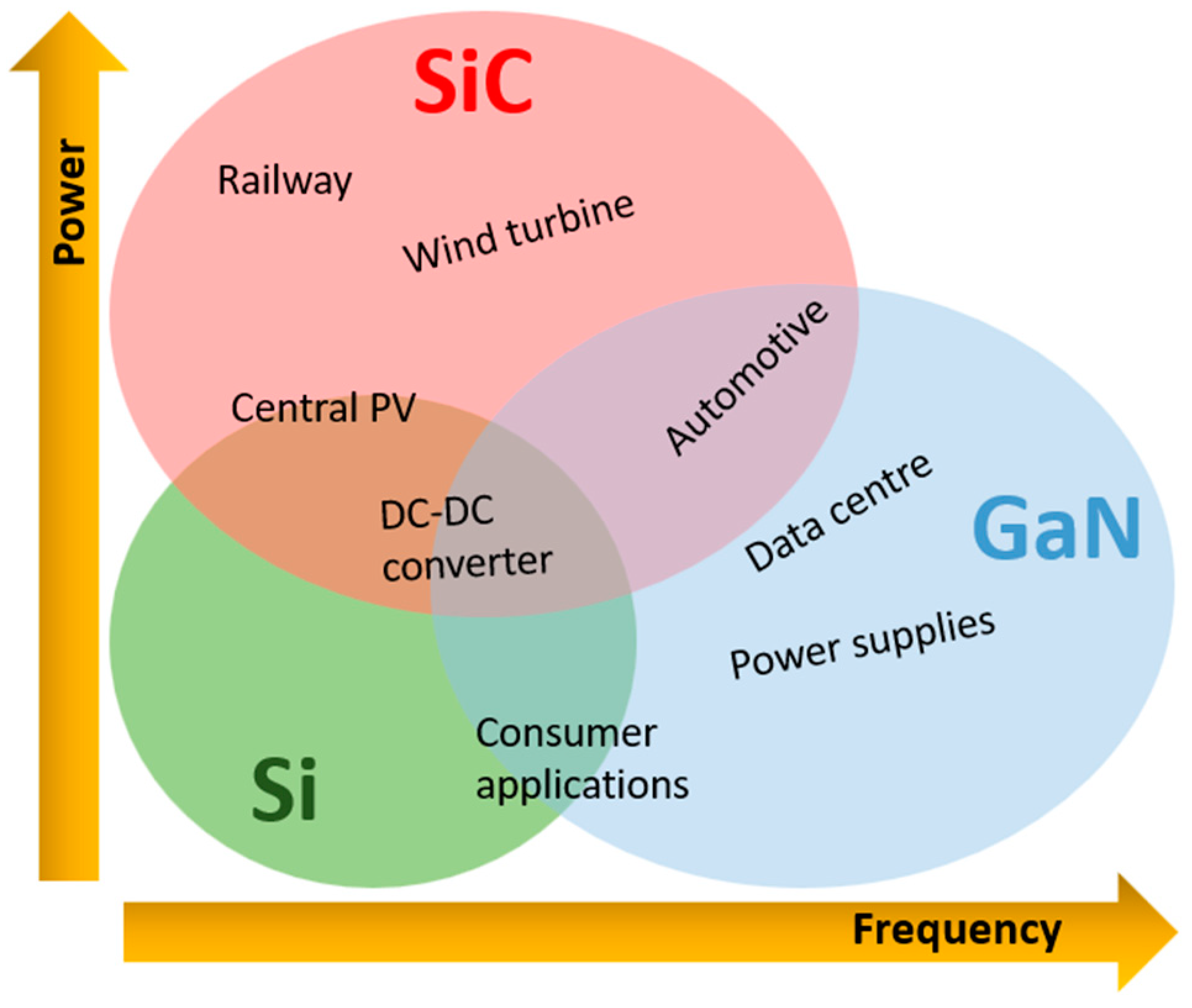
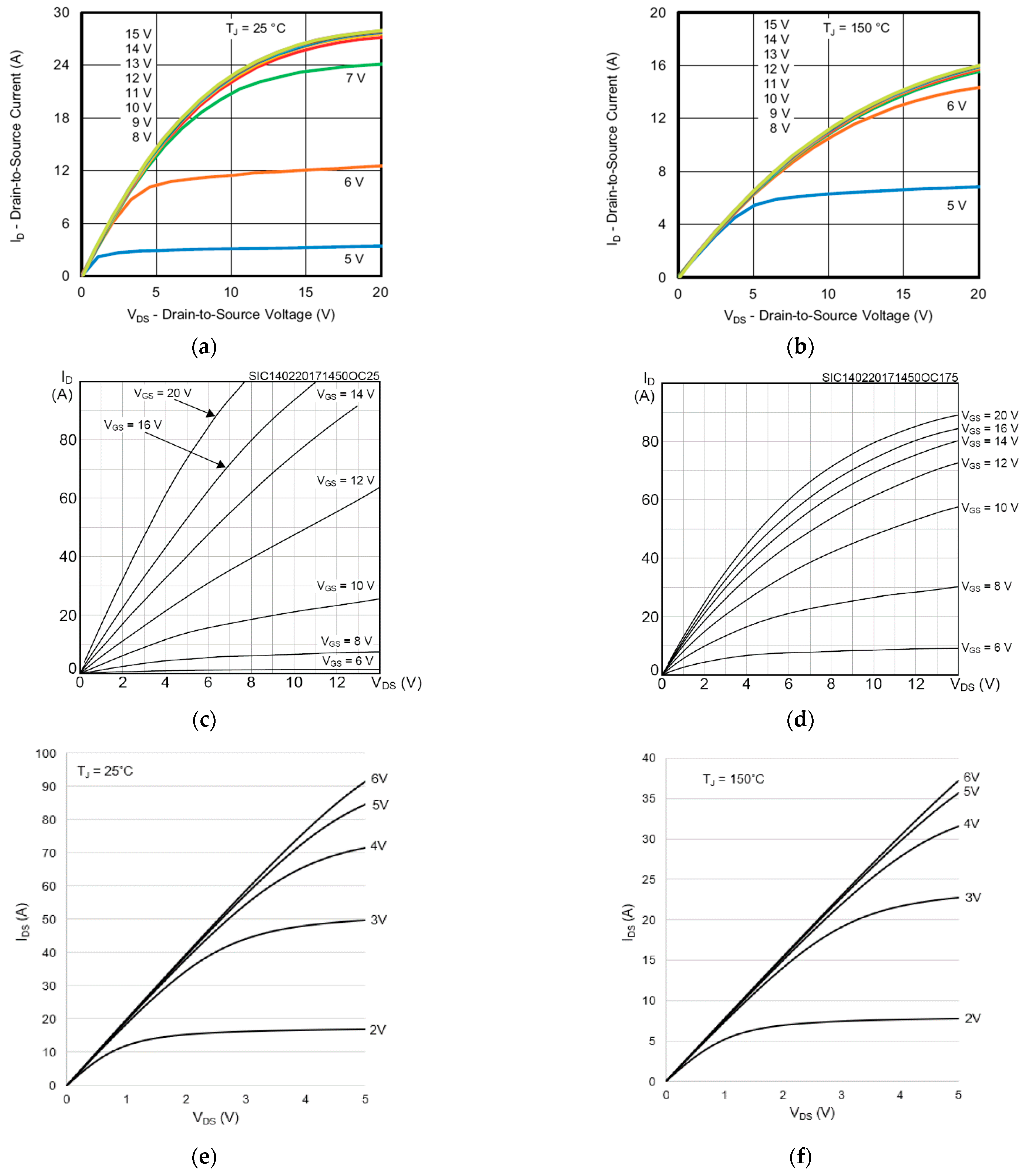
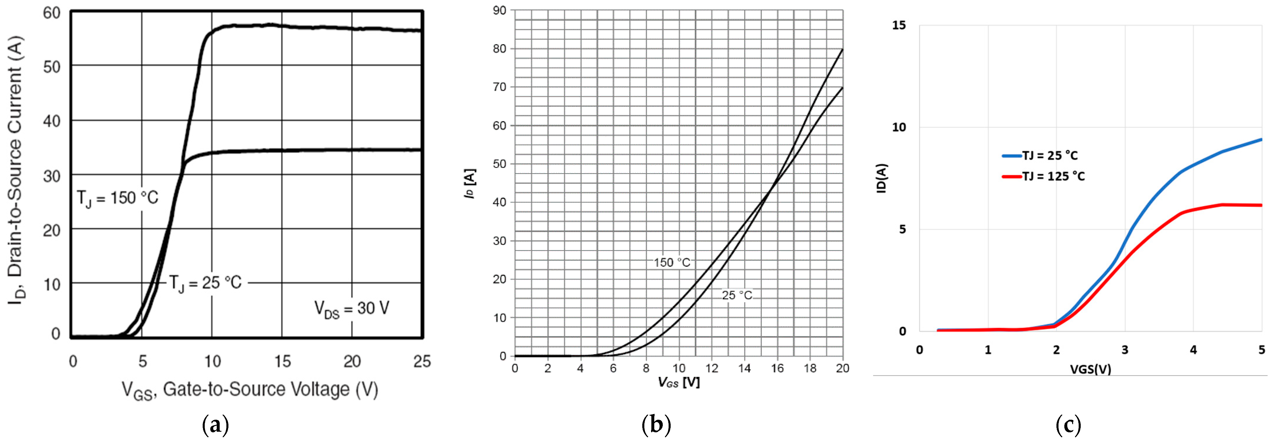
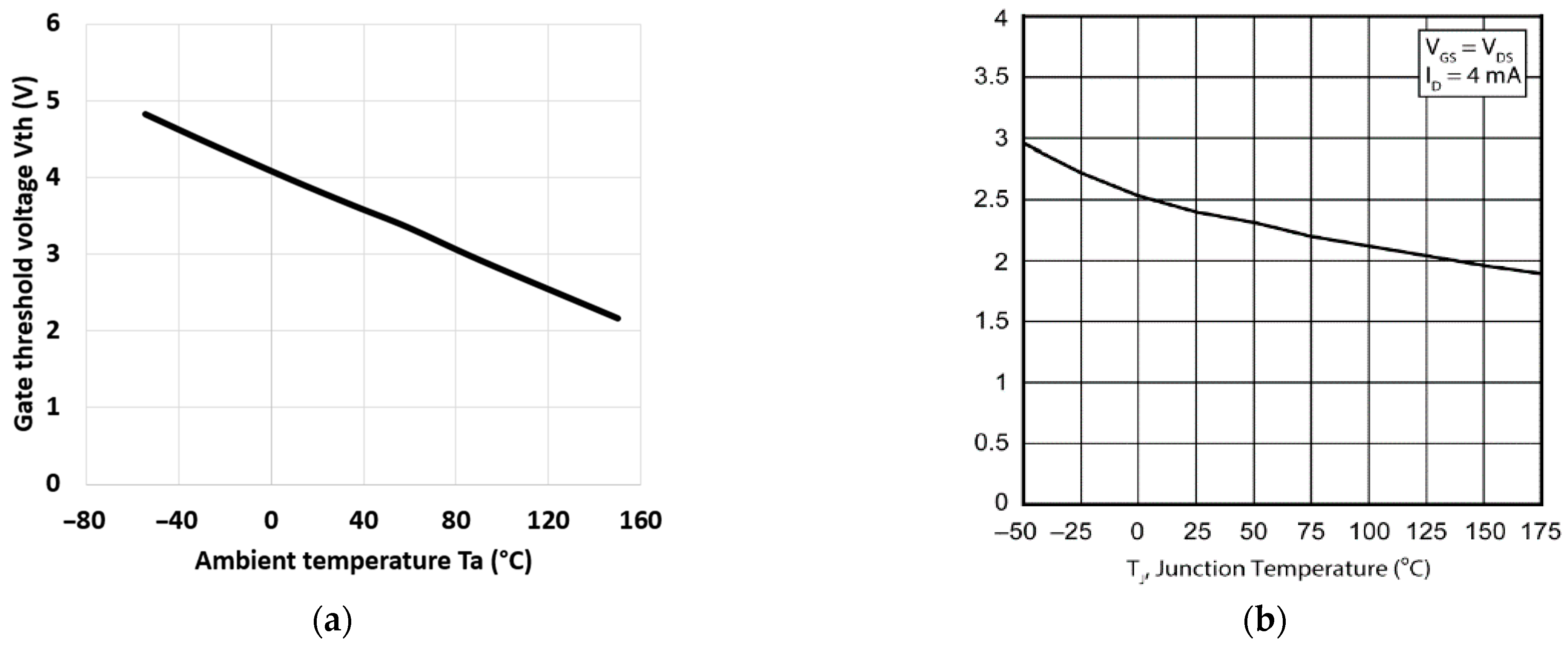
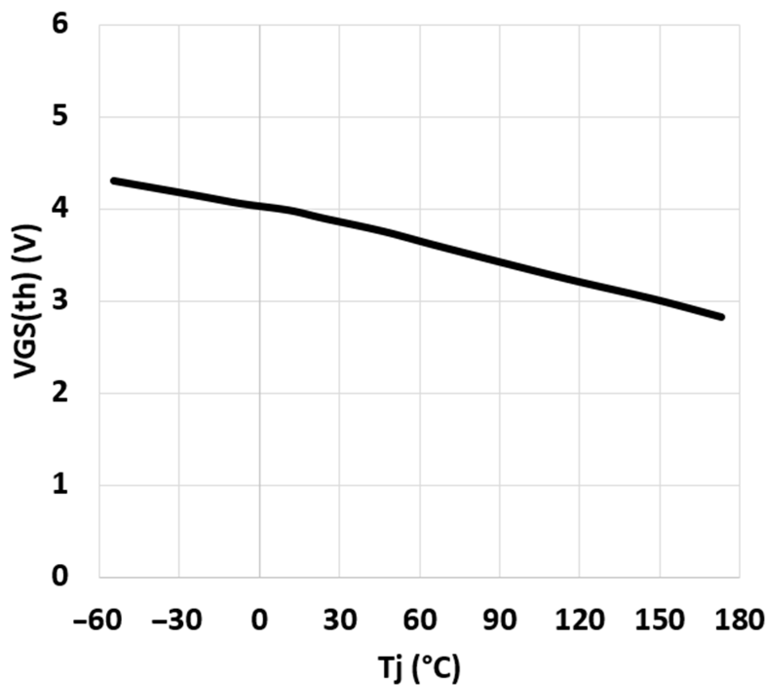
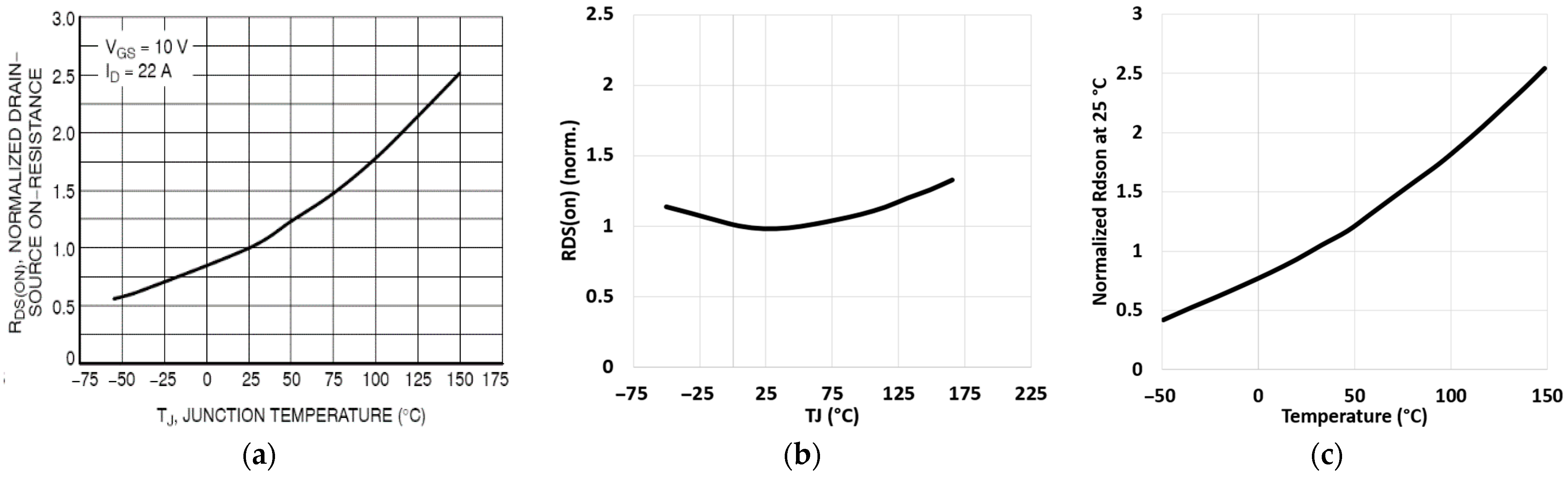
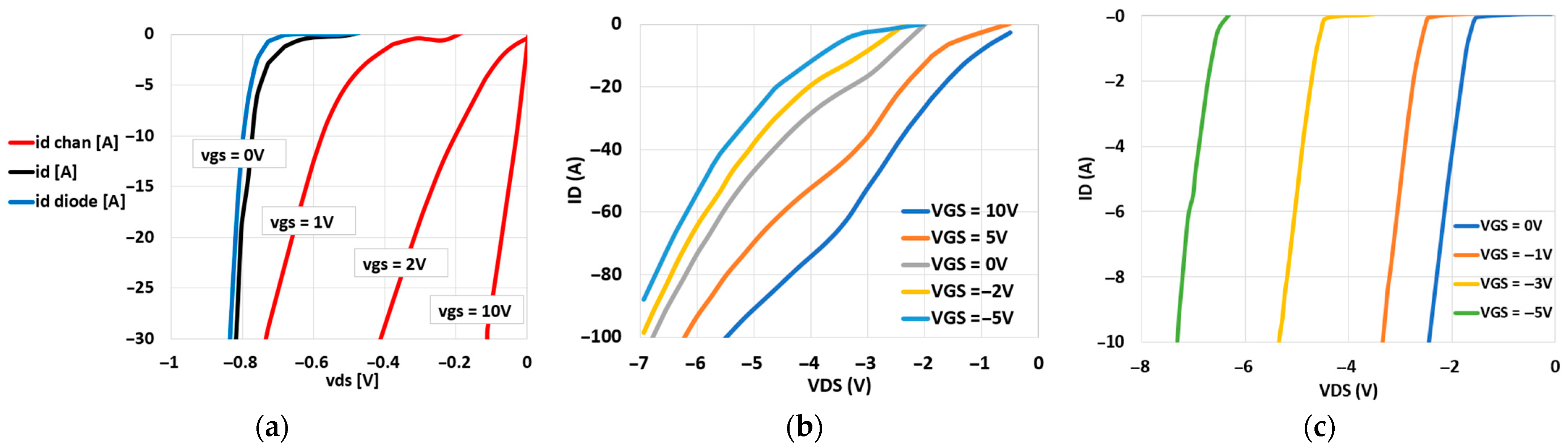
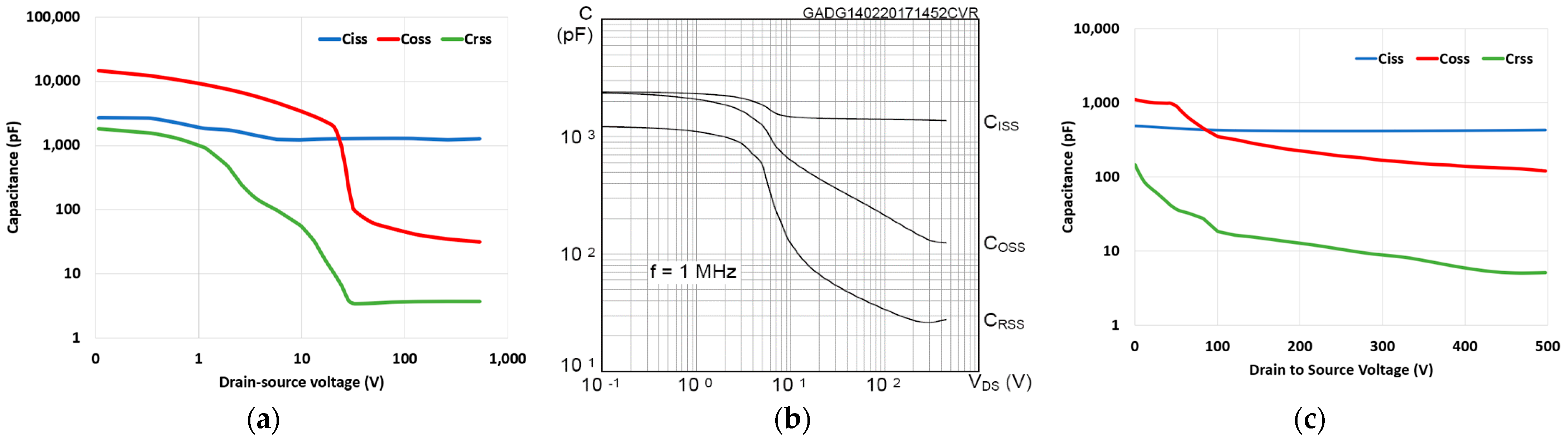
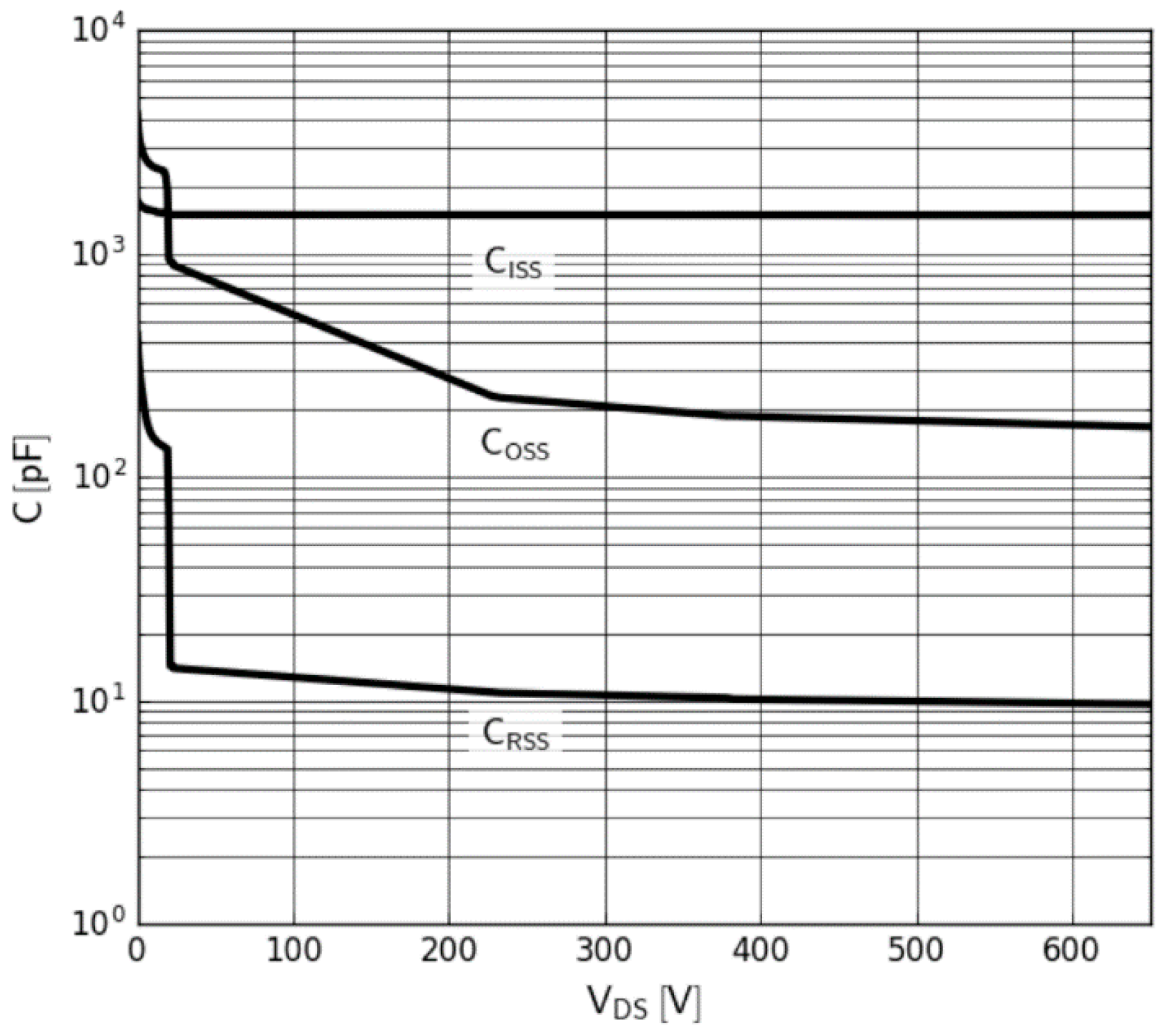
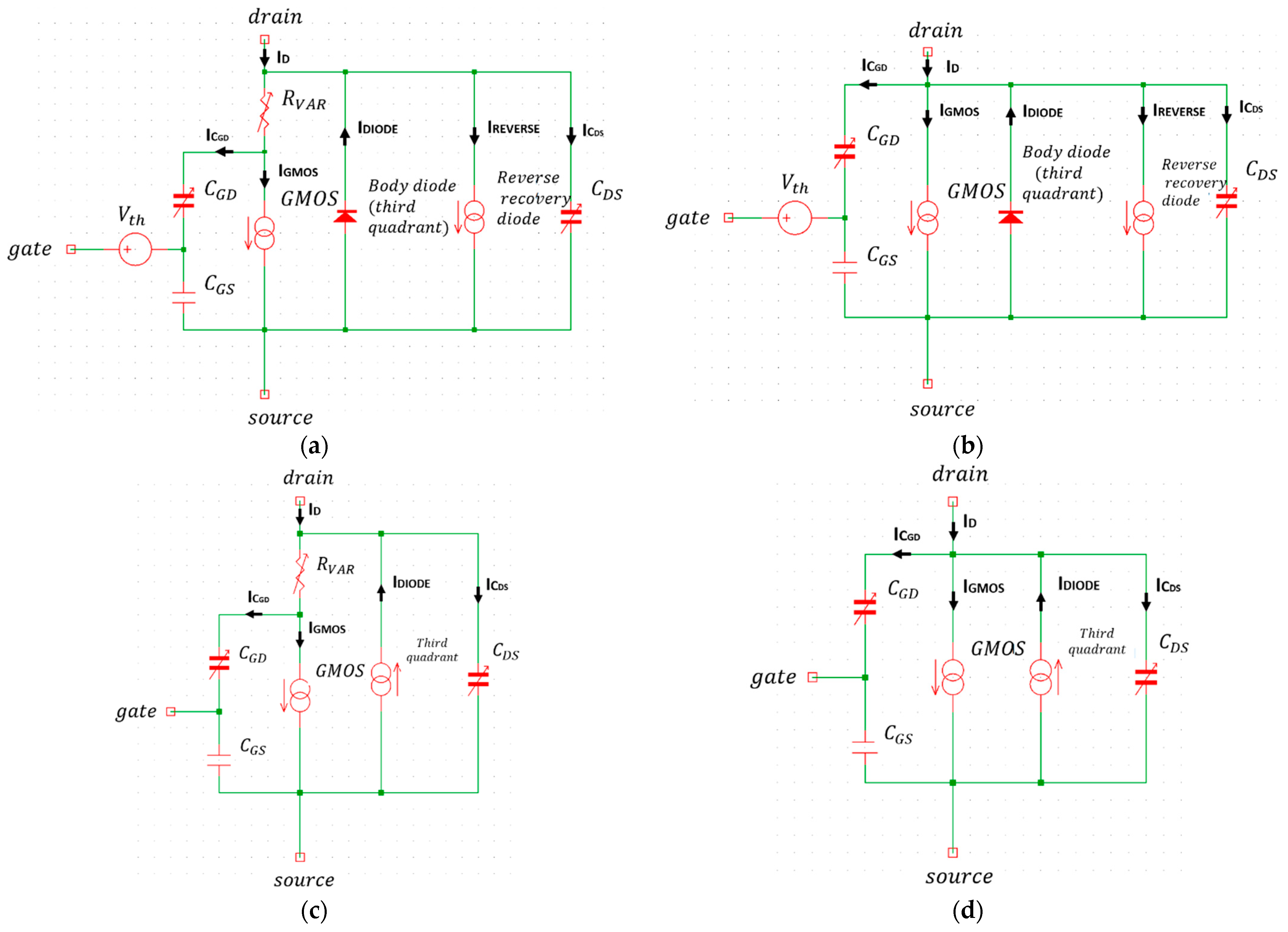
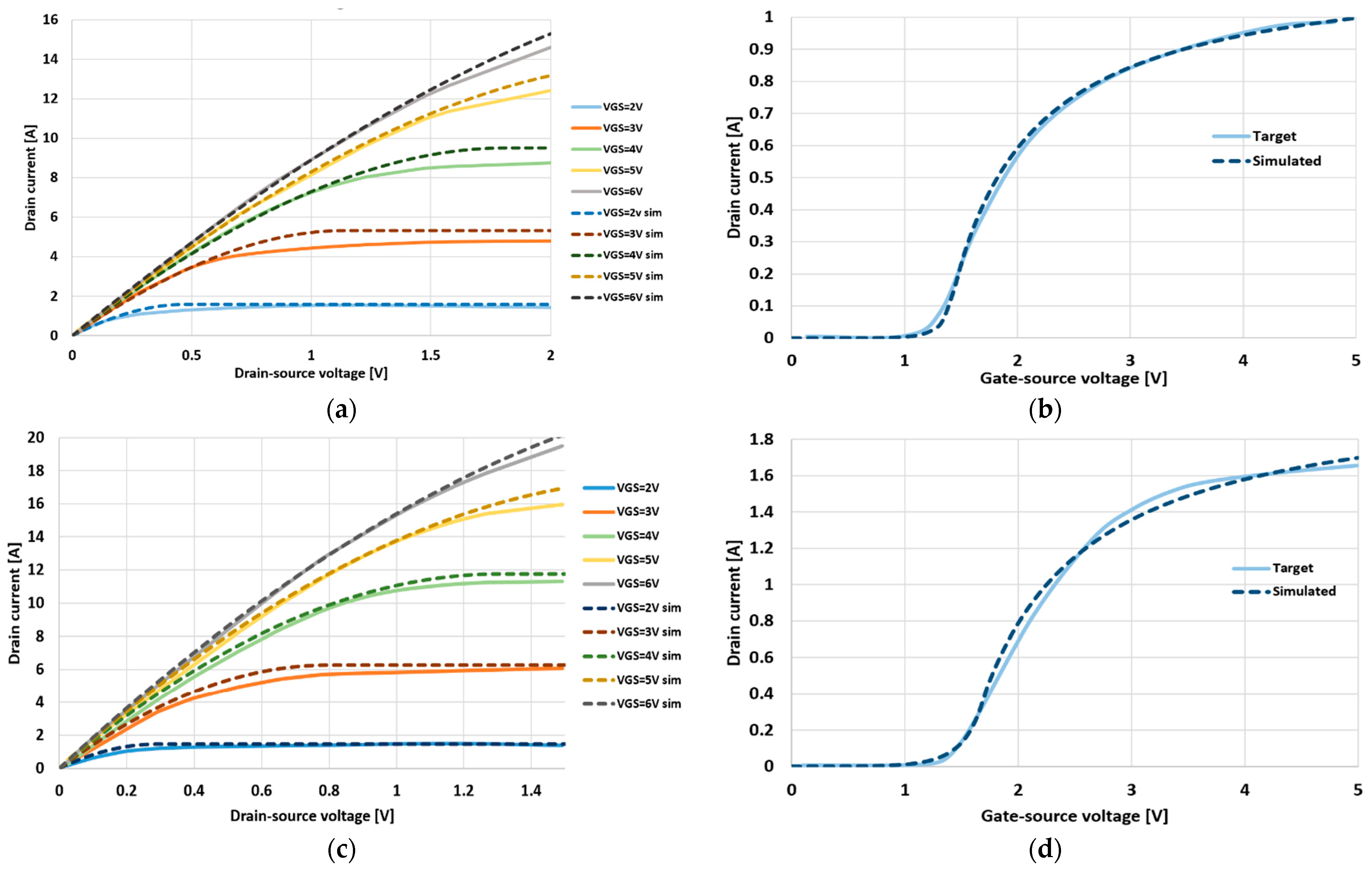
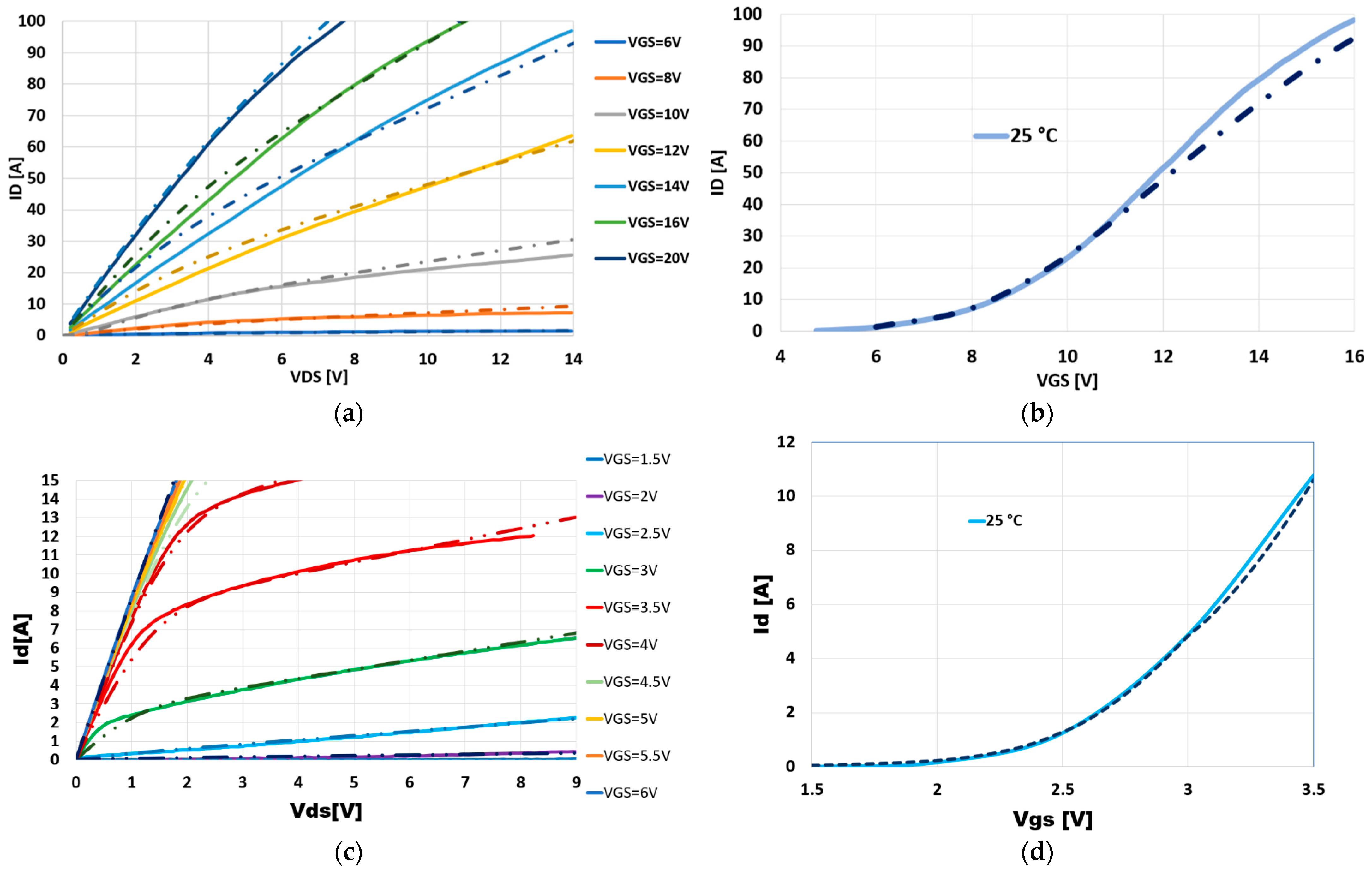
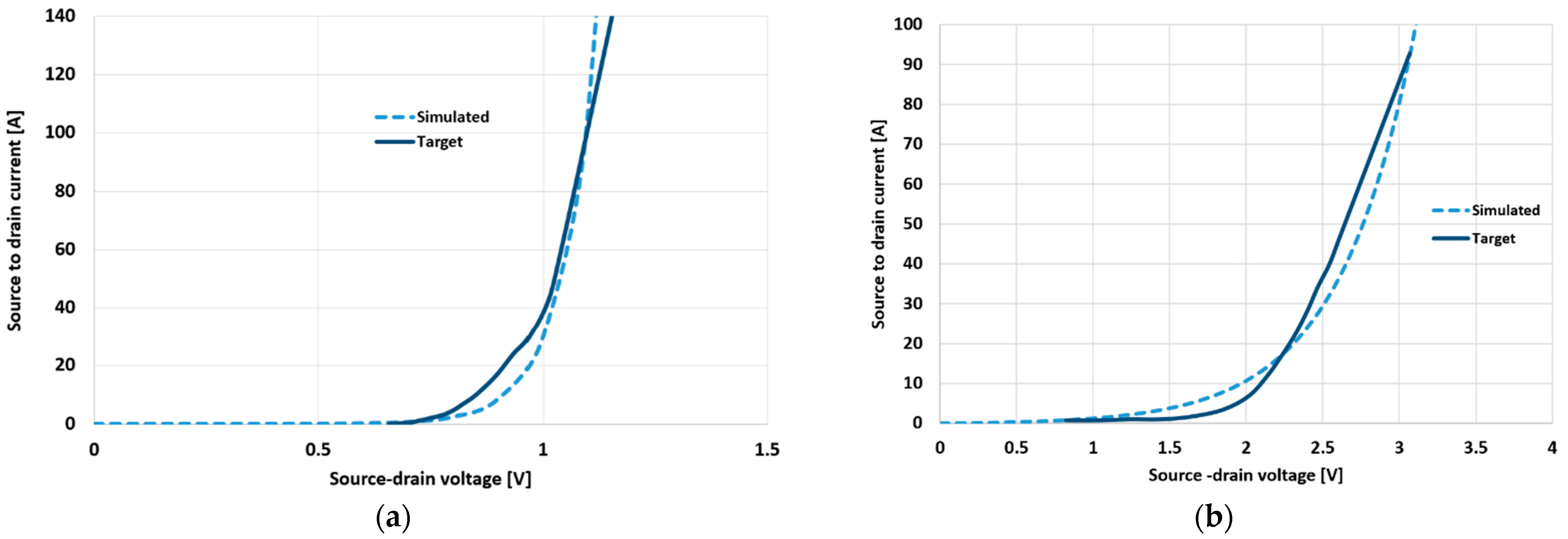
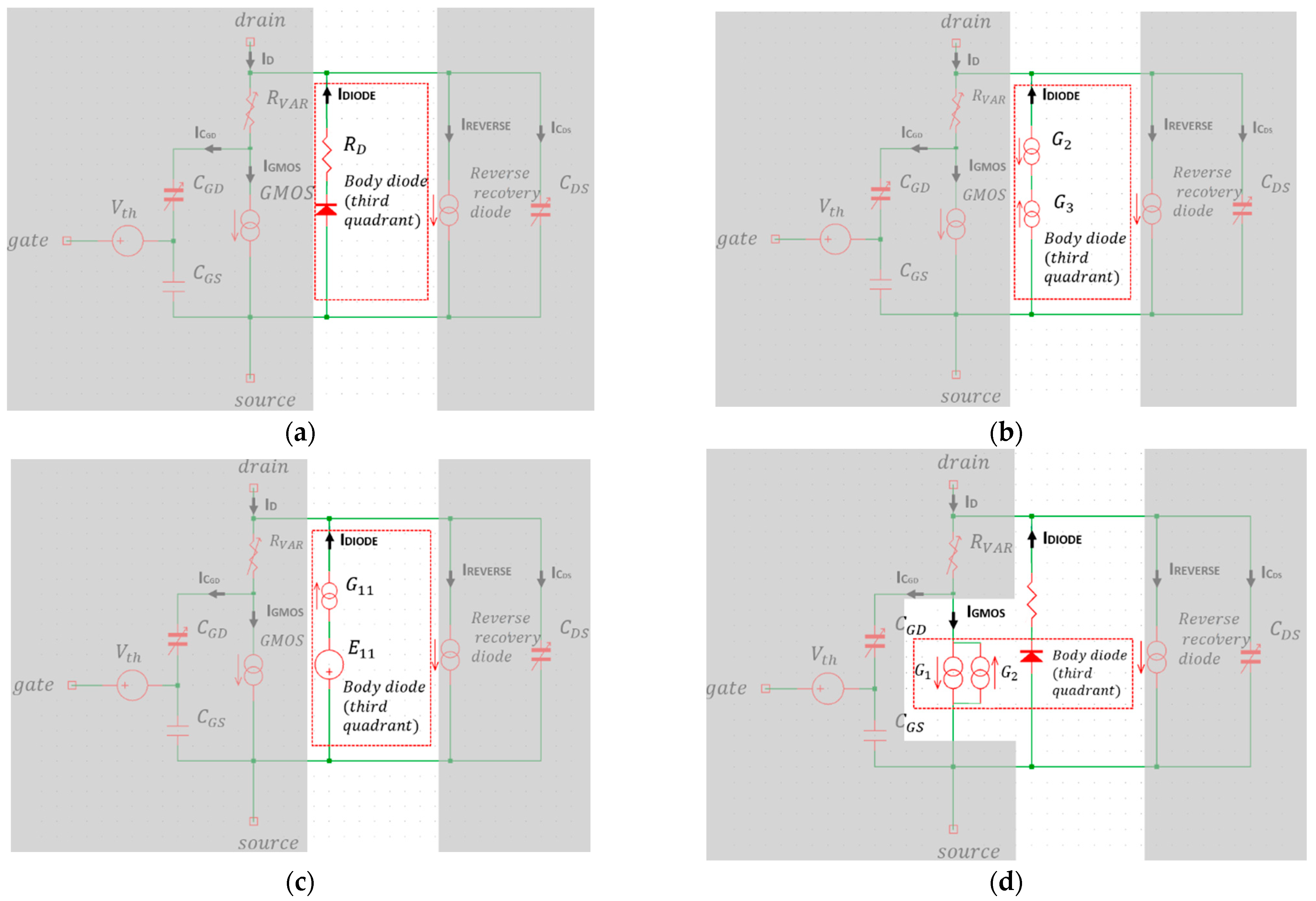
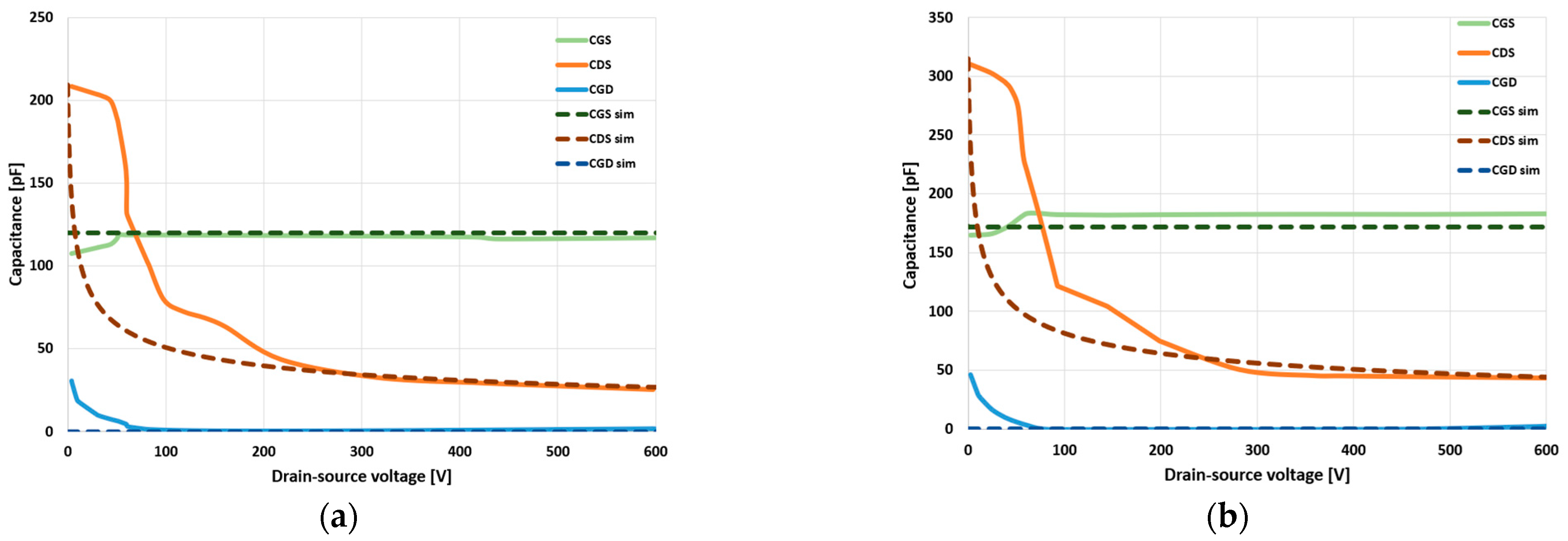
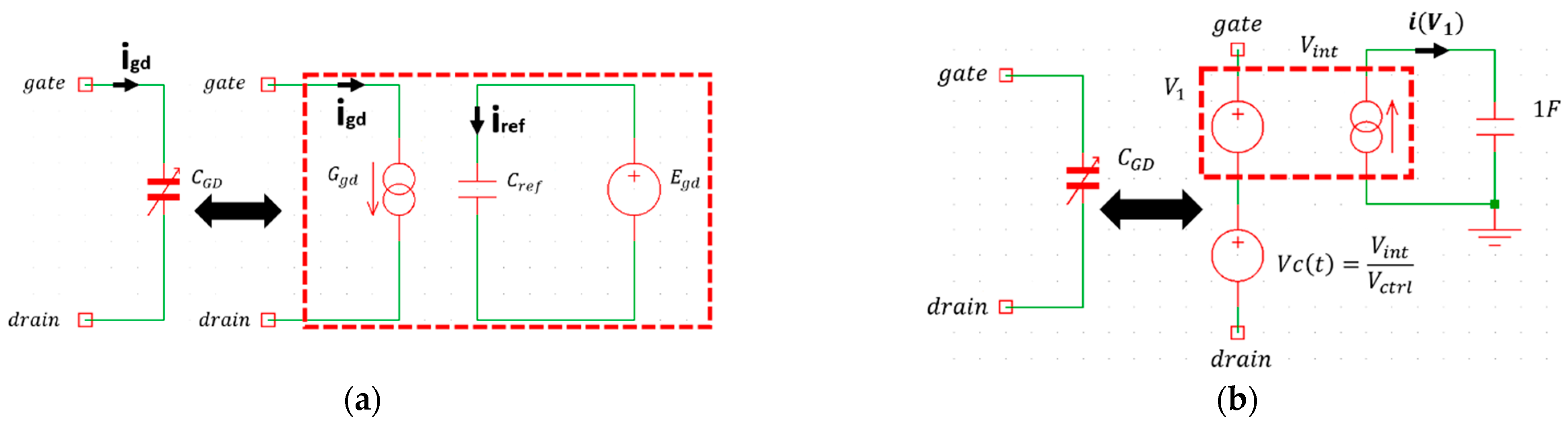
Table 1.
GaN modelling: usability of equations adopted in MOSFET models. Legend: ✓ valid; ● adaptable; x useless; - not reported.
Table 1.
GaN modelling: usability of equations adopted in MOSFET models. Legend: ✓ valid; ● adaptable; x useless; - not reported.
| Model | GMOS | VTH | RVAR | Third Quadrant | Capacitance |
|---|---|---|---|---|---|
| [58] | ● | - | x | ● | ✓ |
| [62] | ✓ | - | - | - | ● |
| [66] | ● | - | - | ✓ | ● |
| [67] | ✓ | - | - | - | - |
| [69] | ● | - | - | ● | ✓ |
| [71] | ✓ | - | - | - | - |
| [72] | ✓ | - | ● | - | ● |
| [73] | ✓ | - | - | - | - |
| [75] | ✓ | - | - | - | - |
| [76] | ● | - | - | - | - |
| [77] | ✓ | - | - | - | - |
| [78] | ✓ | - | - | - | - |
| [80] | ● | - | - | ● | - |
| [81] | ✓ | x | x | - | - |
| [82] | ✓ | x | - | - | - |
| [83] | - | x | x | - | - |
| [84] | - | - | ✓ | - | - |
| [85] | - | - | - | ✓ | ✓ |
| [88] | - | - | - | - | ● |
| [89] | - | - | - | - | ● |
| [90] | - | - | - | - | ✓ |
| [91] | - | - | - | - | ✓ |
| [92] | - | - | - | - | ✓ |
Publisher’s Note: MDPI stays neutral with regard to jurisdictional claims in published maps and institutional affiliations. |
© 2022 by the authors. Licensee MDPI, Basel, Switzerland. This article is an open access article distributed under the terms and conditions of the Creative Commons Attribution (CC BY) license (https://creativecommons.org/licenses/by/4.0/).
Share and Cite
MDPI and ACS Style
Bottaro, E.; Rizzo, S.A.; Salerno, N. Circuit Models of Power MOSFETs Leading the Way of GaN HEMT Modelling—A Review. Energies 2022, 15, 3415. https://doi.org/10.3390/en15093415
AMA Style
Bottaro E, Rizzo SA, Salerno N. Circuit Models of Power MOSFETs Leading the Way of GaN HEMT Modelling—A Review. Energies. 2022; 15(9):3415. https://doi.org/10.3390/en15093415
Chicago/Turabian StyleBottaro, Enrico, Santi Agatino Rizzo, and Nunzio Salerno. 2022. "Circuit Models of Power MOSFETs Leading the Way of GaN HEMT Modelling—A Review" Energies 15, no. 9: 3415. https://doi.org/10.3390/en15093415
Note that from the first issue of 2016, this journal uses article numbers instead of page numbers. See further details here.