A Survey on Bidirectional DC/DC Power Converter Topologies for the Future Hybrid and All Electric Aircrafts

 , and
, and
Abstract
:1. Introduction
- Study of a wide set of relevant topologies for HVDC/LVDC application.
- Efficiency optimization in a wide voltage input and output operation range defined by specific aeronautic standards, as well a as wide load range.
- Losses break down analysis.
- Estimation of passives weight.
- Filters are included in all topologies to achieve similar versatile control features, and comparable filtering features.
- Switching frequencies considered in this study are oriented to high power density designs.
2. Analisys
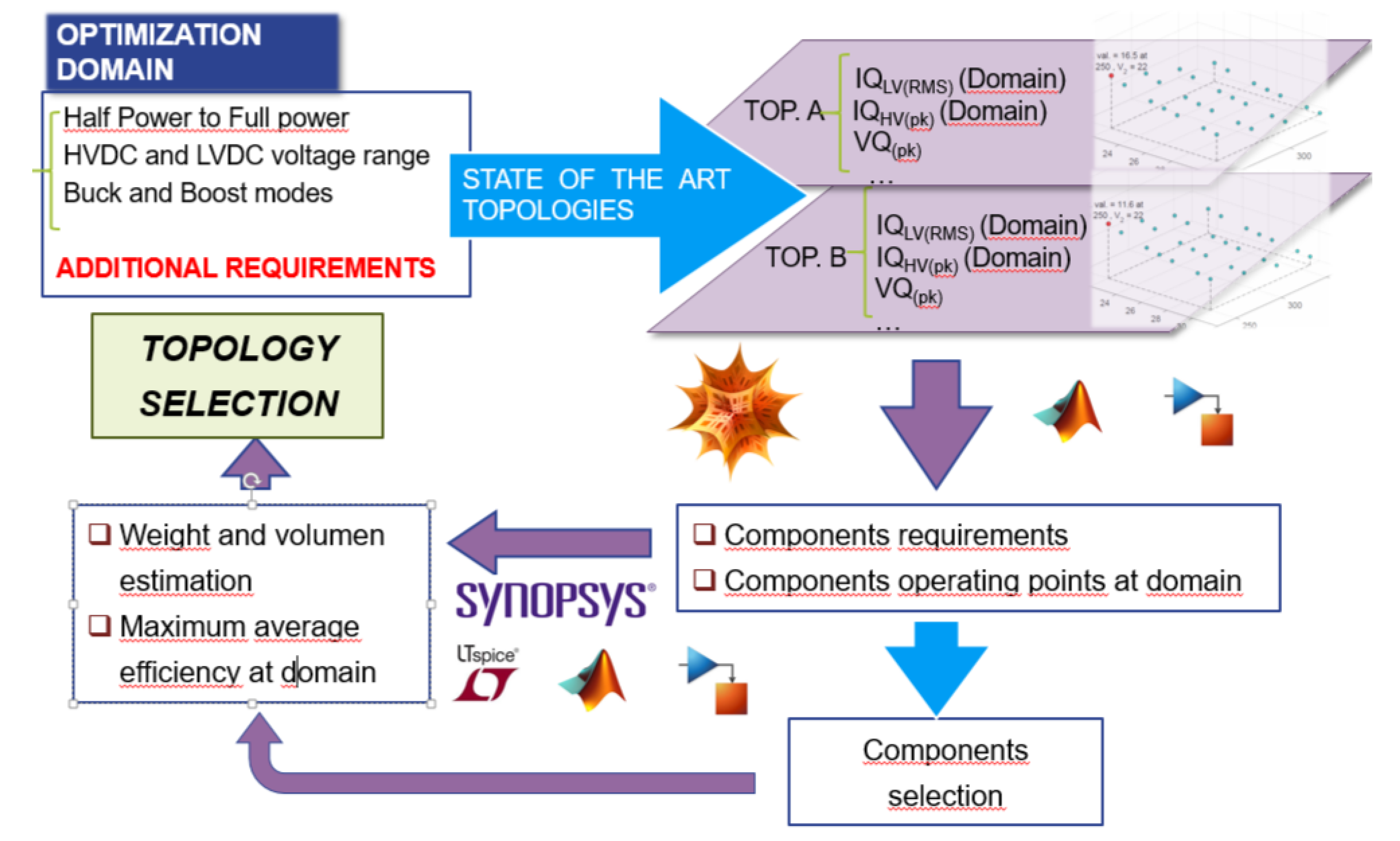
2.1. Methodology
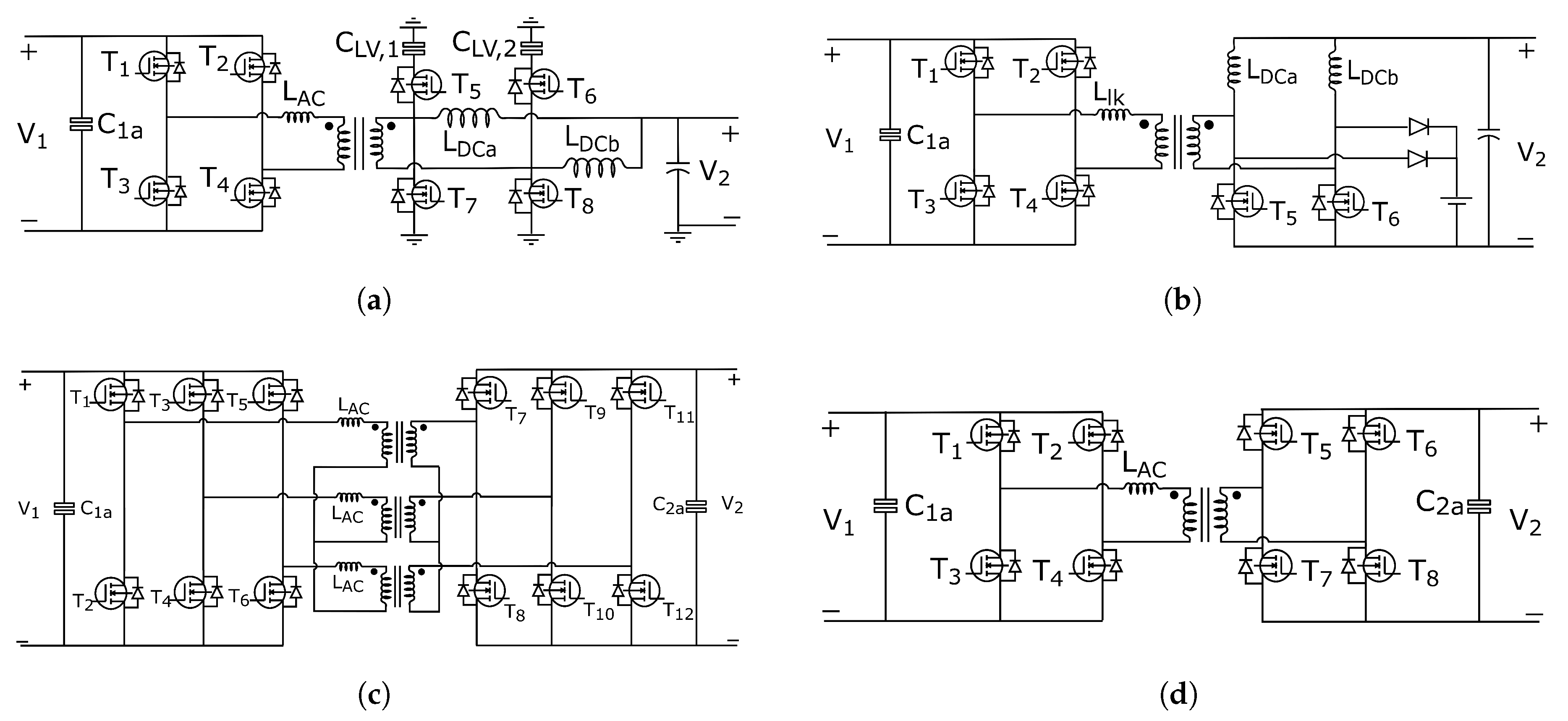
2.2. Topologies Design Considerations
- Transformer turns ratio is typically a half of that for DAB.
- LV components currents change between buck and boost modes.
- Voltage sourced half bridges are floating, instead of a full bridge connected to the LV bus.
- LV floating buses voltage is twice the LV bus voltage.
- A DC inductor is connected to the output of each LV half bridge.
- C1a: RMS current ripple in HV bridges bus due to converter switching operation must be lower than 1% nominal HVDC voltage. Capacitance must be greater than 10 uF (6.6 uF in case of 3p-DAB) due to control aspects.
- C2a: RMS current ripple in LV bridges of DAB topologies bus due to converter switching operation must be lower than 1% of nominal LVDC voltage. Capacitance must be greater than 1 mF (6.6 mF in case of 3p-DAB) due to control aspects.
- CLV,1, CLV,2 in ABAC: Ripple in the worse case must be lower than 5% of RMS LVDC bus nominal voltage.
- LDCa, LDCb in CD. See Figure 2b). Minimum inductance value to ensure that peak to peak current ripple of the sum of inductors currents is less than 40% of LV output current in all considered operating voltages, at nominal power.
- LDCa, LDCb in ABAC: See Figure 2a). Minimum inductance value to ensure that peak to peak current ripple of each inductor current is less than 80% of a half of LV output current, in all considered operating voltages, at nominal power.
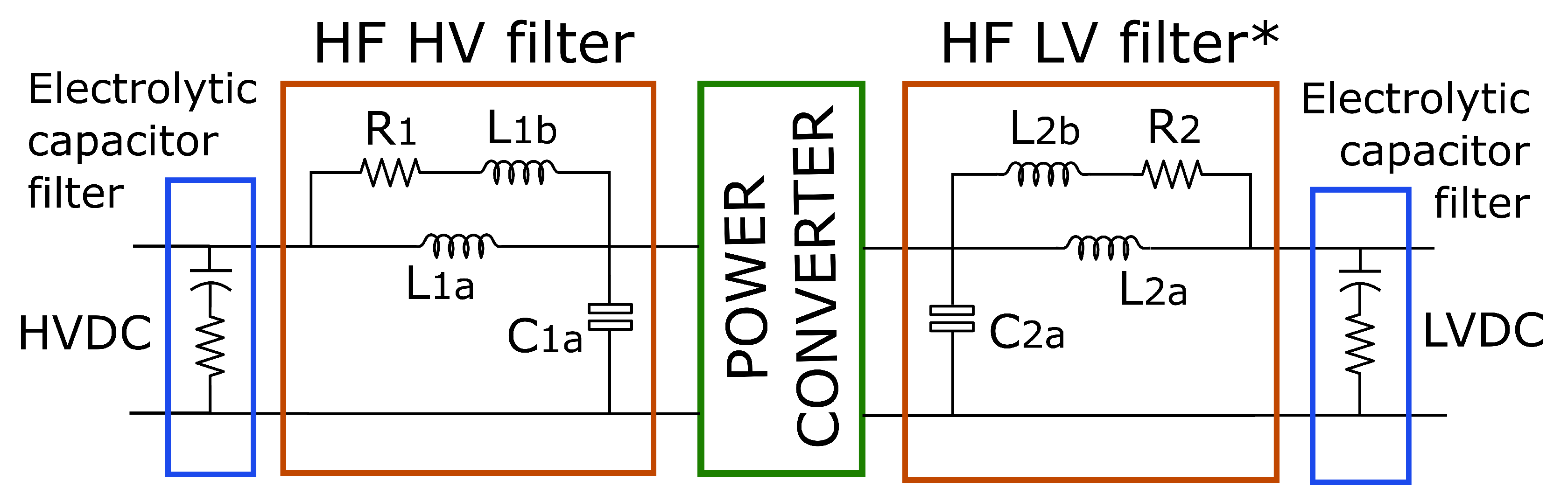
- L1a,L1b, R1: Damped inductor network present in all topologies. Included for current control and short circuit control capabilities (Figure 3). Resonance with is set to 15 kHz (23 kHz for 3p-DAB). = 2 . = 3 , where is the undamped resonator characteristic impedance.
- L2a,L2b, R2: Damped inductor network present in all DAB topologies. Included for current control and short circuit control capabilities (Figure 3). Resonance with is set to 15 kHz (23 kHz for 3p-DAB). = 2 . = 3 , where is the undamped resonator characteristic impedance.
- Limiting ripple of half bridges floating capacitors is desirable for modulation purposes. Therefore, capacitor banks are required.
- Ripple fundamental component of each half bridge occurs at the switching frequency, whereas for other topologies it is twice the switching frequency (6 times for DAB-3p DC links).
- AC excitation of DC inductors is very large. This, along with the fact that fundamental frequency is the swiching frequency, make significant the required size of the inductors.
2.3. Components Models
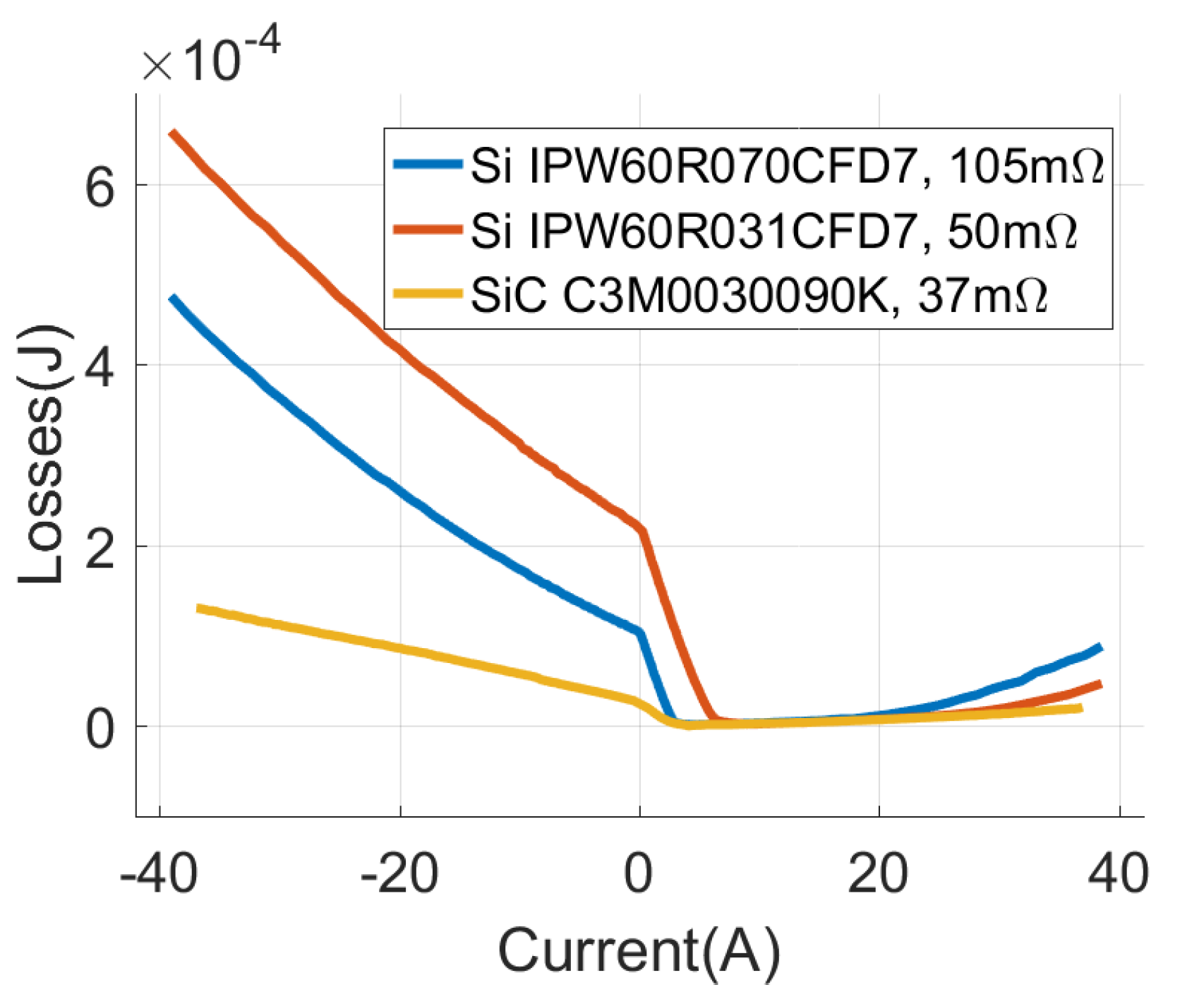
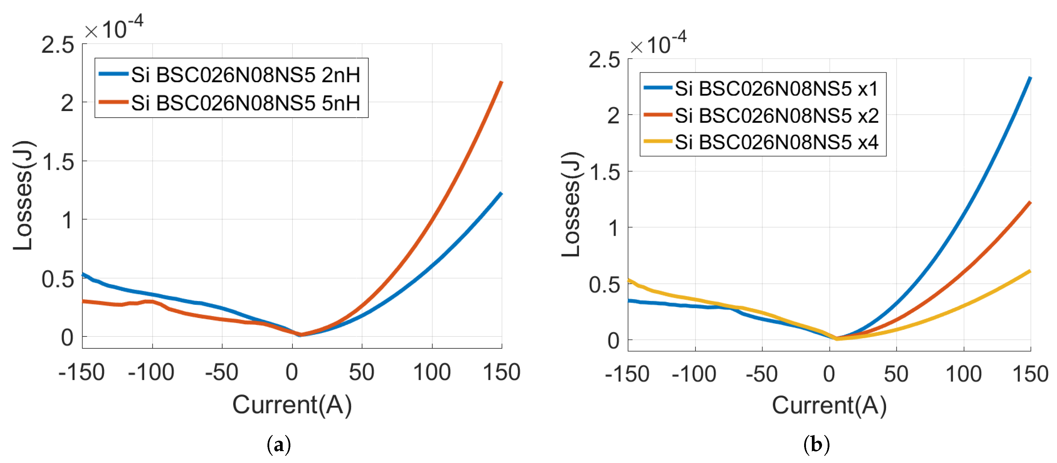
2.3.1. HV MOSFETS
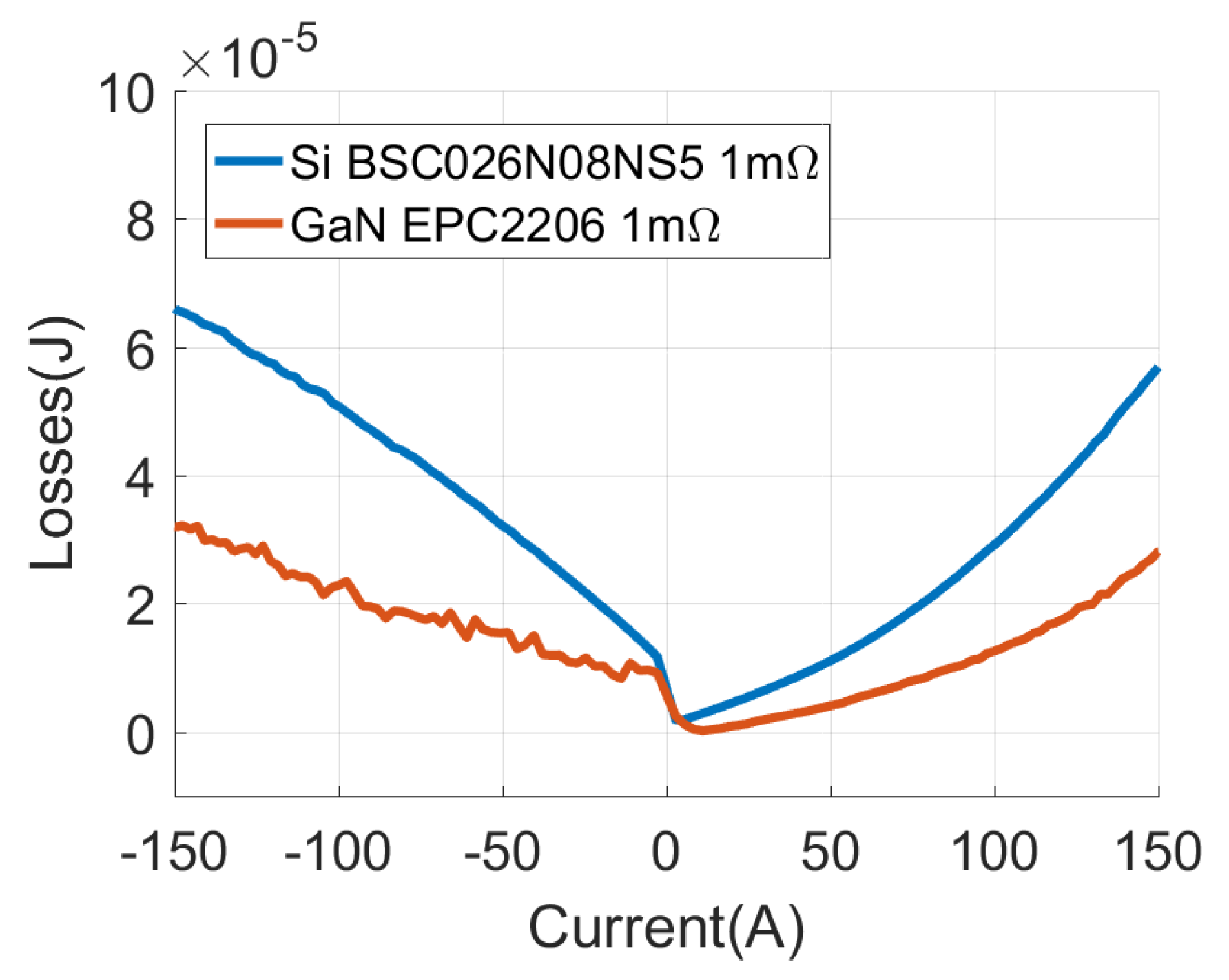
2.3.2. LV MOSFETS
2.3.3. Passives
3. Results
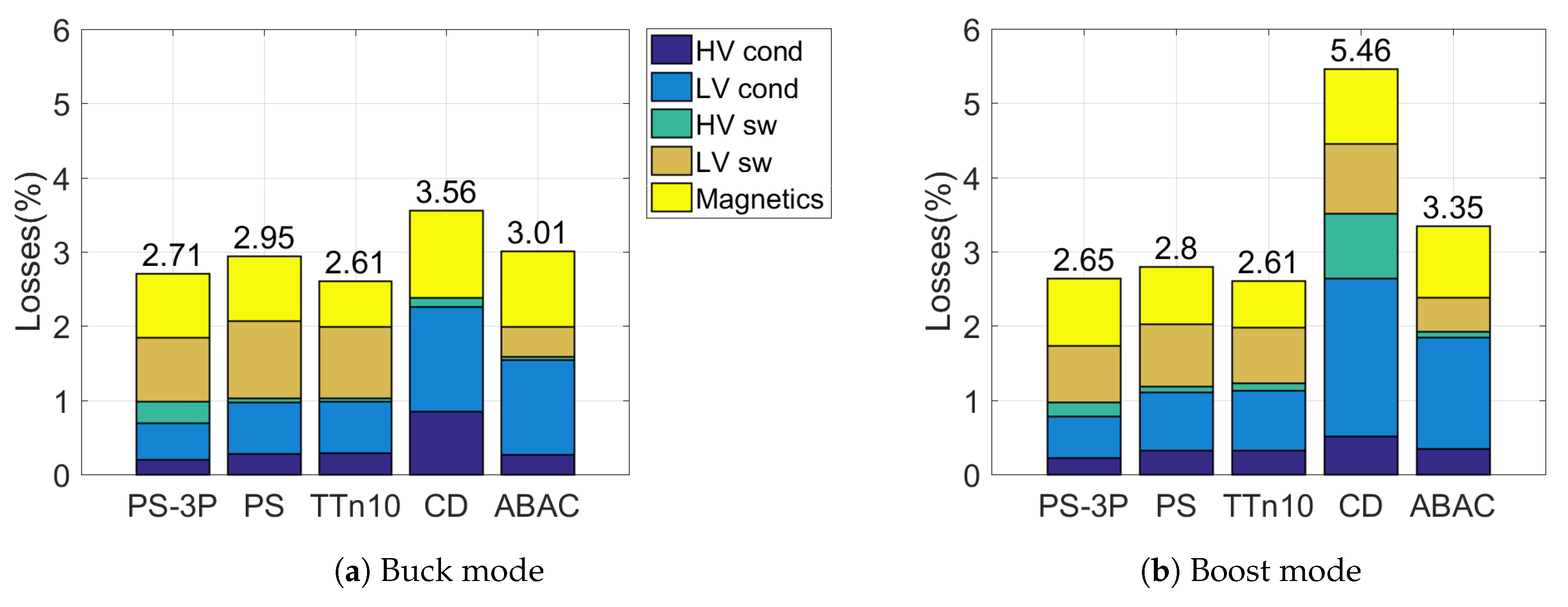
3.1. Efficiency Comparison
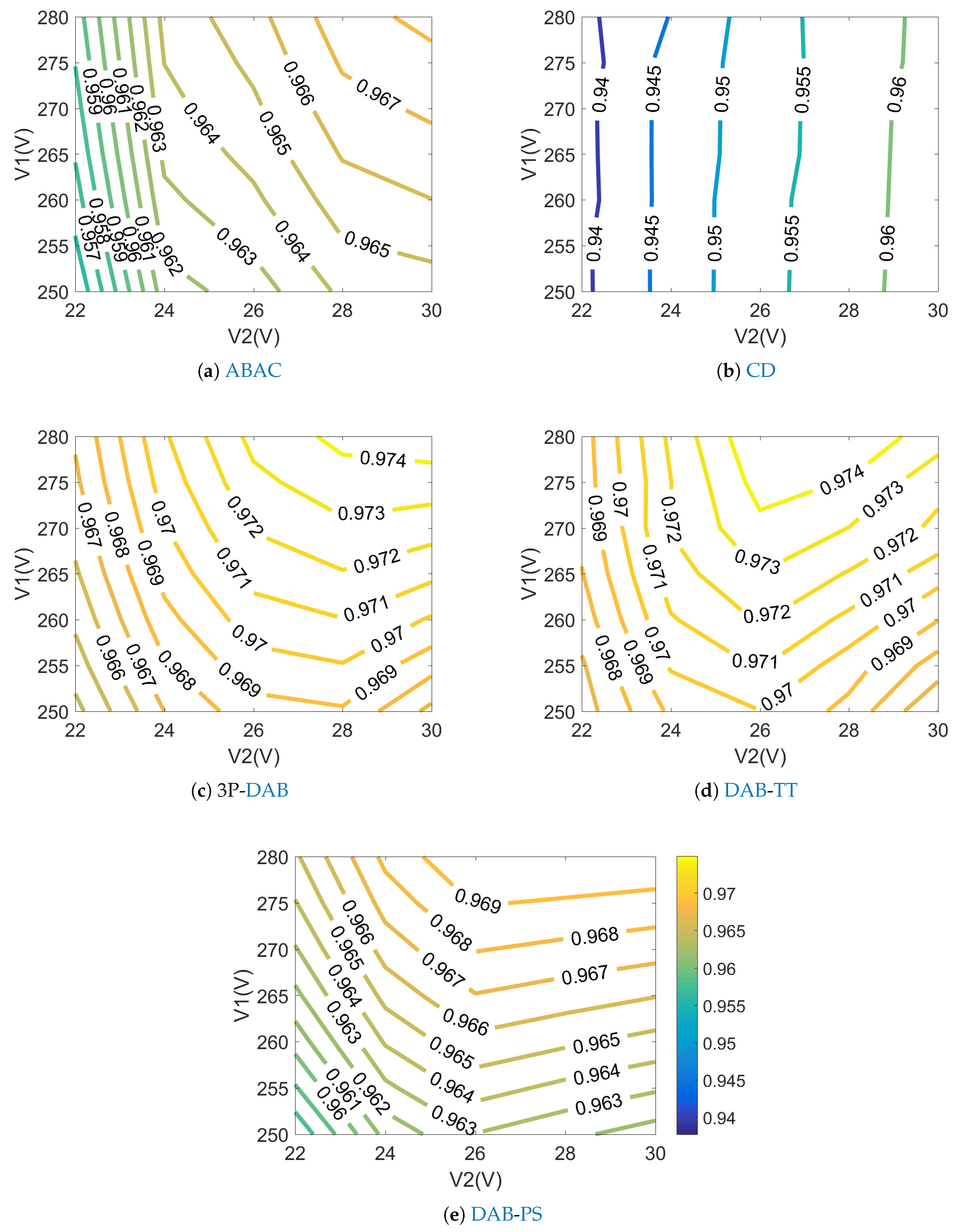
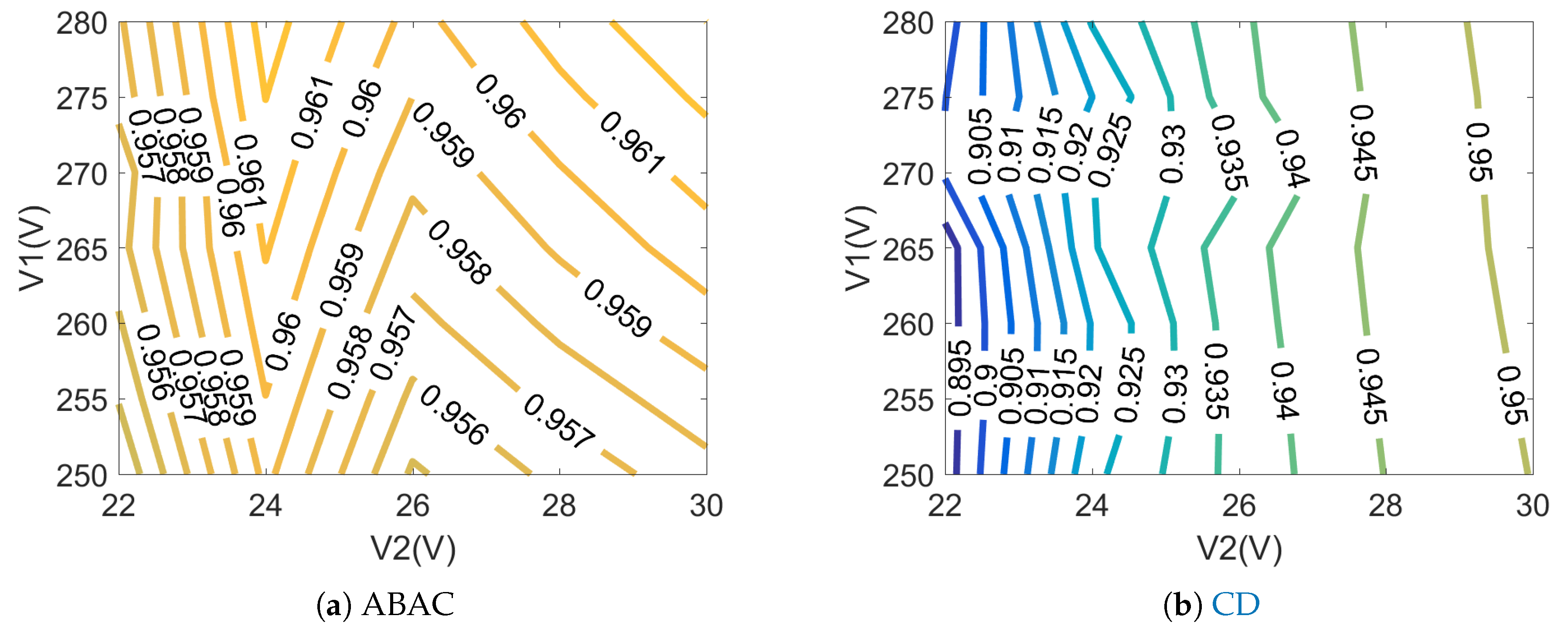
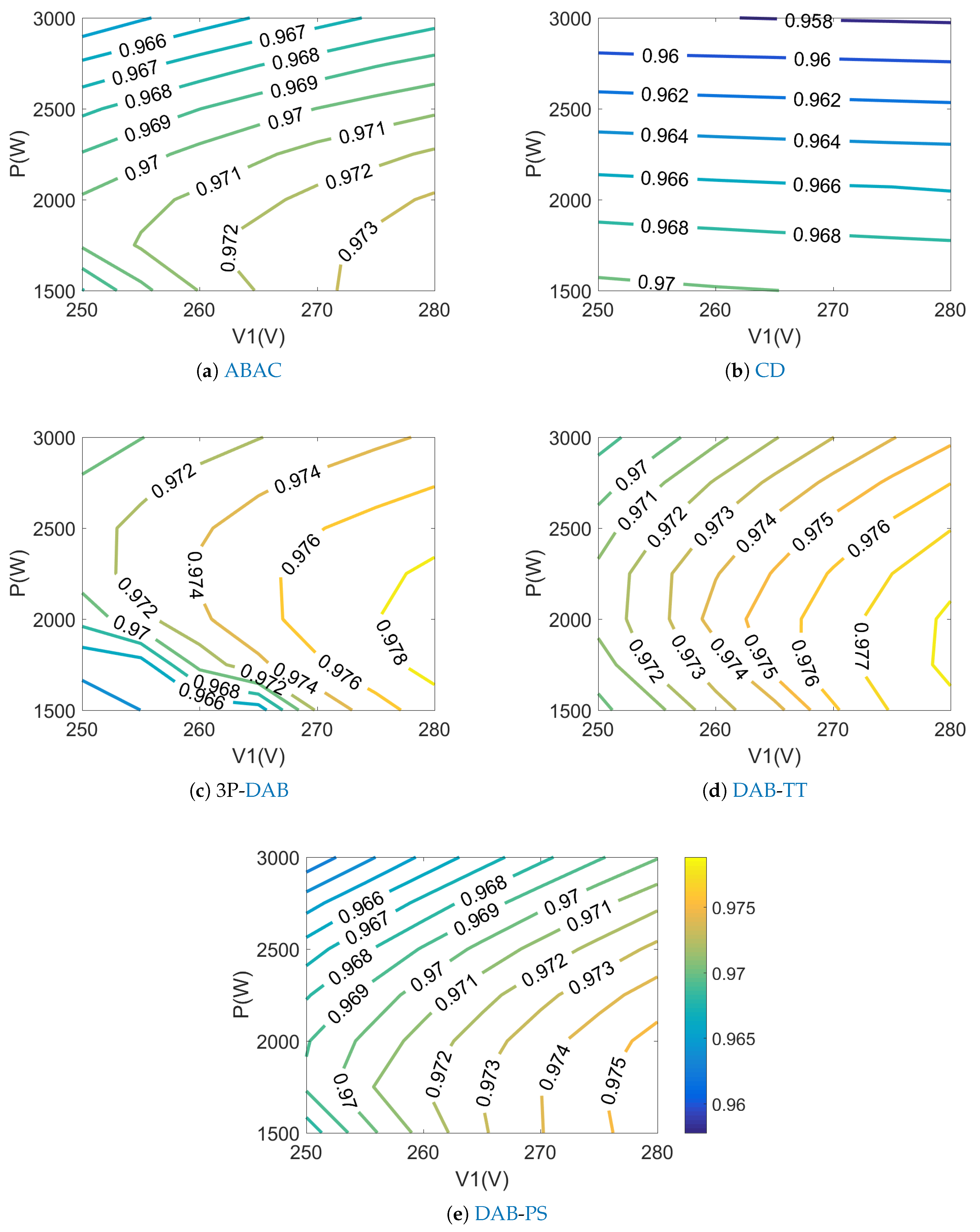
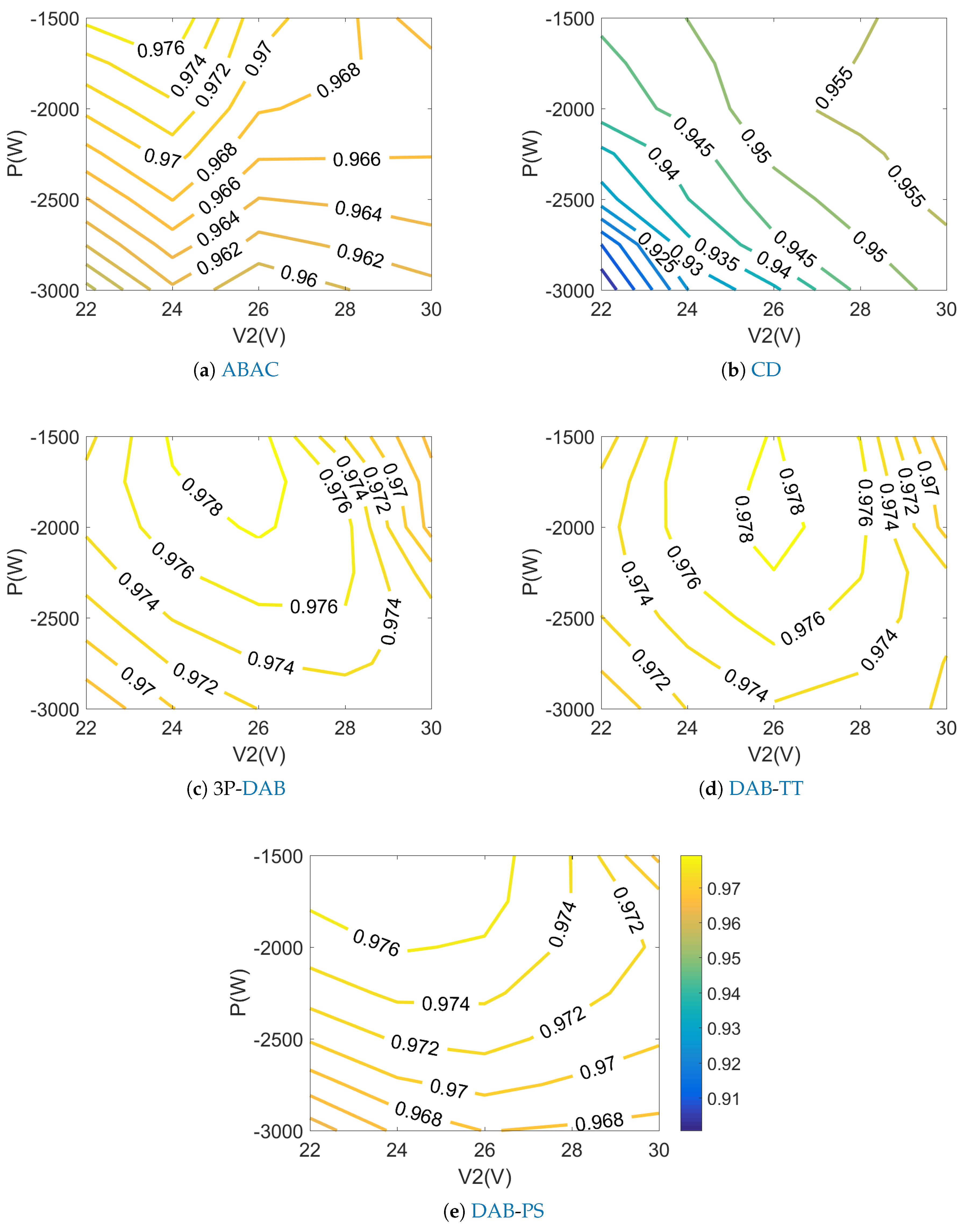
3.1.1. Full Power Efficiency Maps
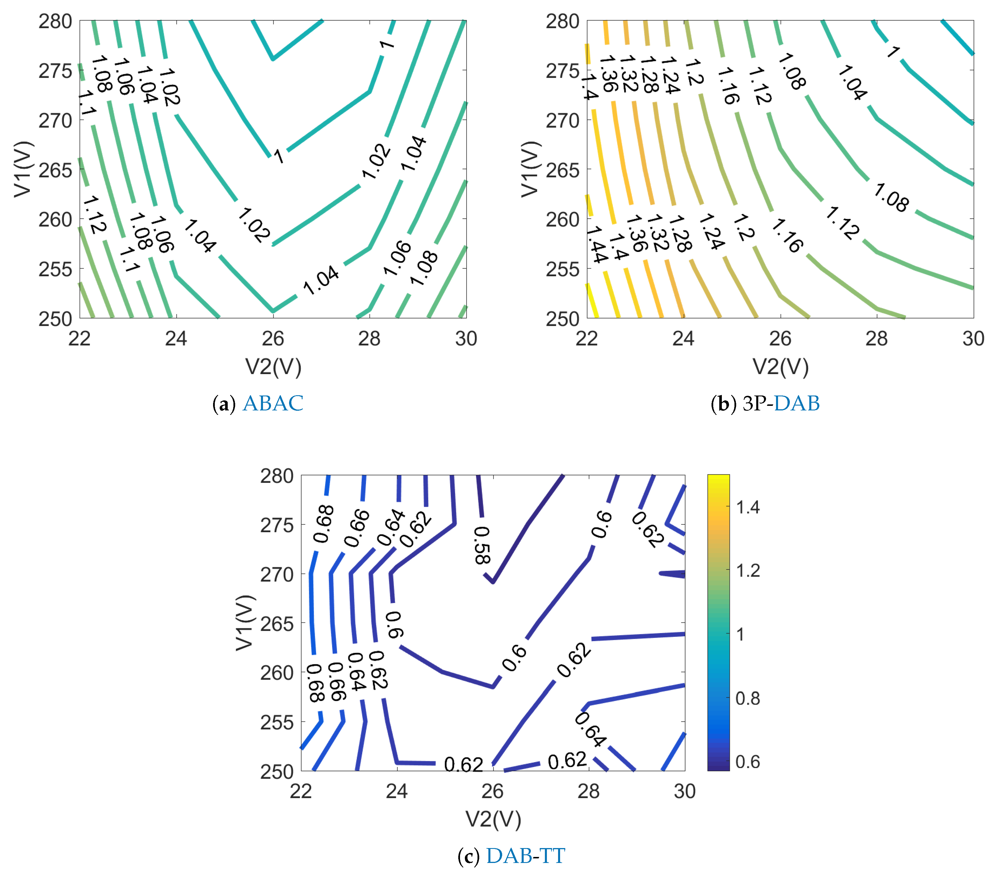
3.1.2. Nominal Output Voltage Efficiency Maps
3.1.3. Average Efficiency Comparison
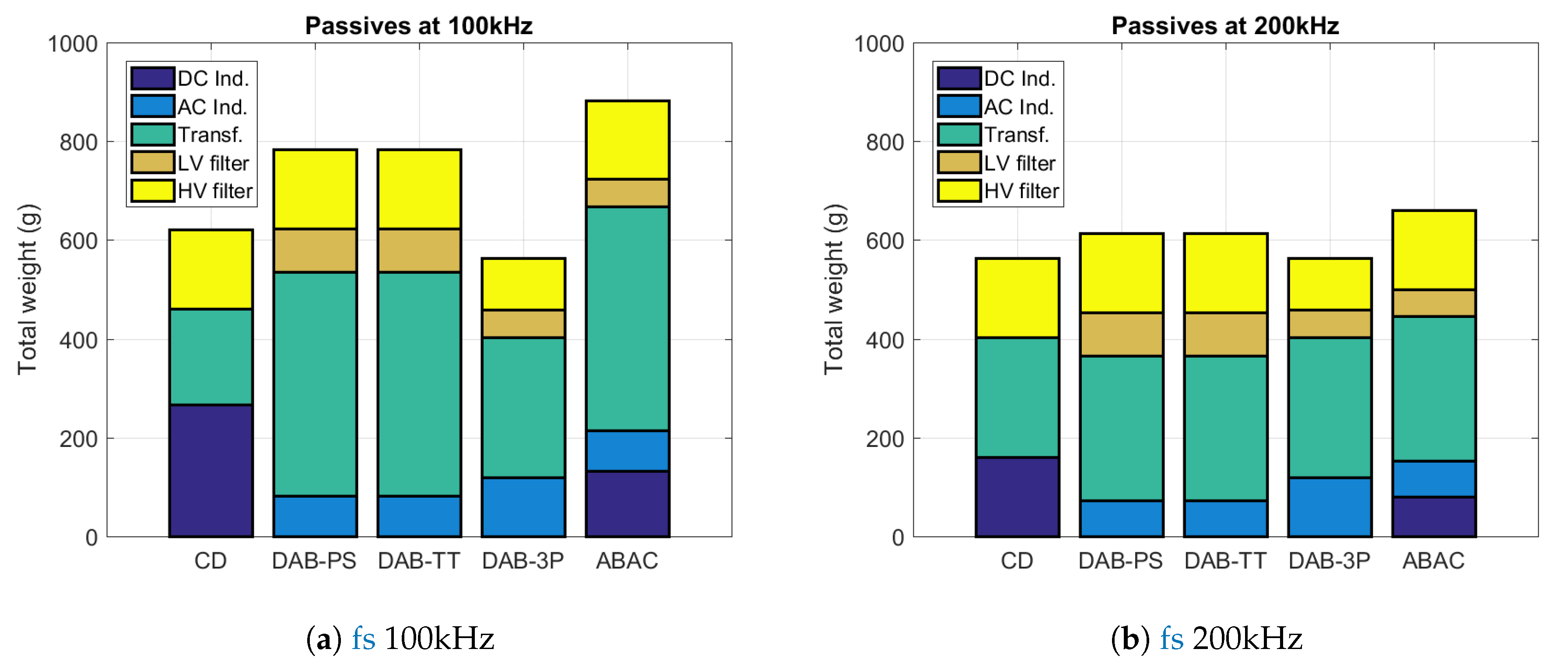
3.2. Weight Estimation
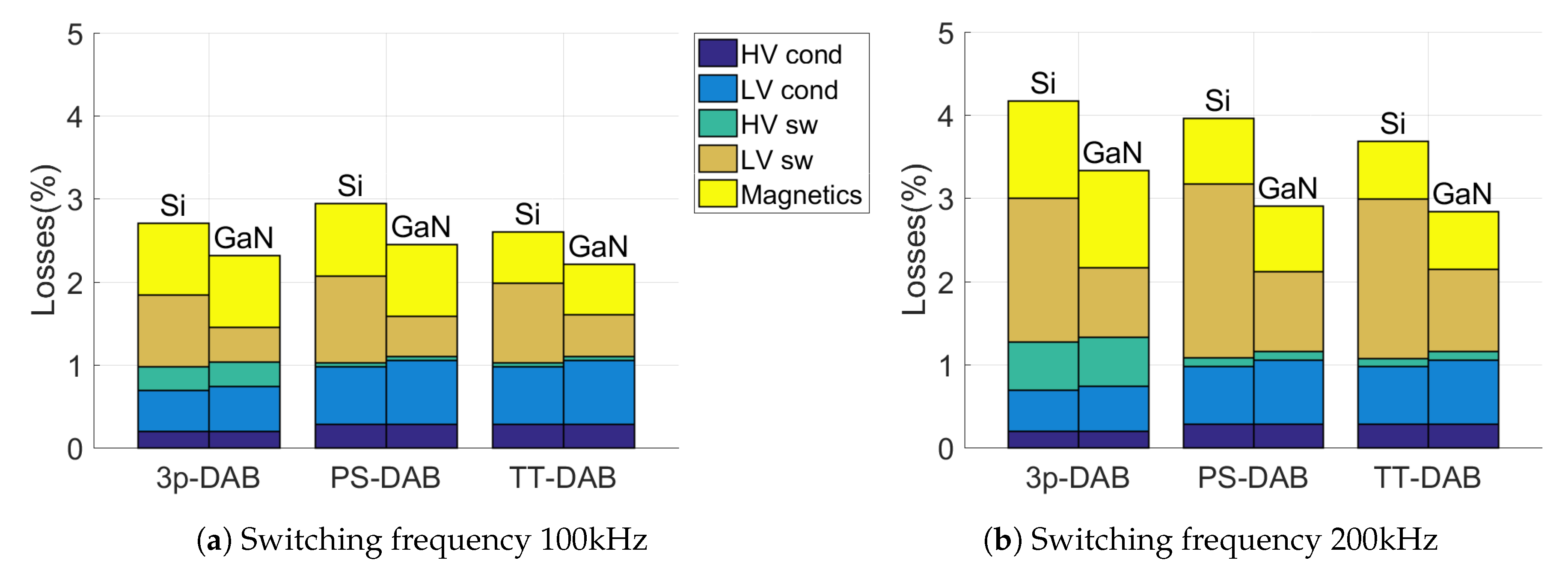
3.3. Efficiencies at 200 kHz and Use of GaN Switches
4. Conclusions
Author Contributions
Funding
Conflicts of Interest
References
- ACARE. Aeronautics and Air Transport: Beyond Vision 2020 (Towards 2050); Technical Report; ACARE (Advisory Council for Aeronautics Research in Europe): Brussels, Belgium, 2010. [Google Scholar]
- Rosero, J.; Ortega, J.; Aldabas, E.; Romeral, L. Moving towards a more electric aircraft. IEEE A E Syst. Mag. 2007, 22, 3–9. [Google Scholar] [CrossRef] [Green Version]
- Roboam, X.; Sareni, B.; De Andrade, A. More Electricity in the air. IEEE Ind. Electron. Mag. 2012, 233–259. [Google Scholar] [CrossRef]
- Sarlioglu, B.; Morris, C.T. More Electric Aircraft: Review, Challenges, and Opportunities for Commercial Transport Aircraft. IEEE Trans. Transp. Electrif. 2015, 1, 54–64. [Google Scholar] [CrossRef]
- Tariq, M.; Maswood, A.I.; Gajanayake, C.J.; Gupta, A.K. Aircraft batteries: Current trend towards more electric aircraft. IET Electr. Syst. Transp. 2017, 7, 93–103. [Google Scholar] [CrossRef]
- Wheeler, P.; Bozhko, S. The more electric aircraft: Technology and challenges. IEEE Electrif. Mag. 2014, 2, 6–12. [Google Scholar] [CrossRef]
- Hartmann, M. Ultra-compact and ultra-efficient Three-phase PWM Rectifier Systems for More Electric Aircraft. Ph.D. Thesis, ETH Zurich, Zurich, Switzerland, 2011. [Google Scholar]
- Chen, J.; Wang, C.; Chen, J. Investigation on the selection of electric power system architecture for future more electric aircraft. IEEE Trans. Transp. Electrif. 2018, 4, 563–576. [Google Scholar] [CrossRef]
- Emadi, A.; Ehsani, M. Aircraft power systems: Technology, state of the art, and future trends. IEEE Aerosp. Electron. Syst. Mag. 2000, 15, 28–32. [Google Scholar] [CrossRef]
- Gao, F.; Bozhko, S.; Costabeber, A.; Asher, G.; Wheeler, P. Control Design and Voltage Stability Analysis of a Droop-Controlled Electrical Power System for More Electric Aircraft. IEEE Trans. Ind. Electron. 2017, 64, 9271–9281. [Google Scholar] [CrossRef]
- Buticchi, G.; Costa, L.F.; Barater, D.; Liserre, M.; Amarillo, E.D. A Quadruple Active Bridge Converter for the Storage Integration on the More Electric Aircraft. IEEE Trans. Power Electron. 2018, 33, 8174–8186. [Google Scholar] [CrossRef] [Green Version]
- Krismer, F. Modeling and Optimization of Bidirectional Dual Active Bridge DC DC Converter Topologies. Ph.D. Thesis, ETH Zurich, Zurich, Switzerland, 2010. [Google Scholar] [CrossRef]
- Kheraluwala, M.N.; Gascoigne, R.W.; Divan, D.M.; Baumann, E.D. Performance Characterization of a High-Power Dual Active Bridge dc-to-dc Converter. IEEE Trans. Ind. Appl. 1992, 28, 1294–1301. [Google Scholar] [CrossRef]
- Bai, H.; Mi, C. Eliminate reactive power and increase system efficiency of isolated bidirectional dual-active-bridge dc-dc converters using novel dual-phase-shift control. IEEE Trans. Power Electron. 2008, 23, 2905–2914. [Google Scholar] [CrossRef]
- Zhao, B.; Song, Q.; Liu, W. Power characterization of isolated bidirectional dual-active-bridge dc-dc converter with dual-phase-shift control. IEEE Trans. Power Electron. 2012, 27, 4172–4176. [Google Scholar] [CrossRef]
- Krismer, F.; Kolar, J.W. Efficiency-optimized high-current dual active bridge converter for automotive applications. IEEE Trans. Ind. Electron. 2012, 59, 2745–2760. [Google Scholar] [CrossRef]
- Flores, L.A.; García, O.; Oliver, J.A.; Cobos, J.A. High-frequency Bi-directional DC/DC converter using two inductor rectifier. IECON Proc. (Ind. Electron. Conf.) 2006, 2793–2798. [Google Scholar] [CrossRef]
- De Doncker, R.W.; Divan, D.M.; Kheraluwala, M. A three-phase soft-switched high power density dc/dc converter for high power applications. IEEE Trans. Ind. Appl. 1991, 27, 63–73. [Google Scholar] [CrossRef]
- Bhat, A.K.S.; Member, S. Fixed-Frequency PWM Series-Parallel Resonant Converter. IEEE Trans. Ind. Appl. 1992, 28, 1002–1009. [Google Scholar] [CrossRef]
- Pan, X.; Li, H.; Liu, Y.; Tianyang, Z.; Ju, C.; Rathore GAE, A.K. An Overview and Comprehensive Comparative Evaluation of Current-Fed Isolated Bidirectional DC/DC Converter. IEEE Trans. Power Electron. 2019, 35, 2737–2763. [Google Scholar] [CrossRef]
- De, D.; Castellazzi, A.; Lamantia, A. 1.2 kW dual-active bridge converter using SiC power MOSFETs and planar magnetics. In Proceedings of the 2014 International Power Electronics Conference, IPEC-Hiroshima—ECCE Asia 2014, Hiroshima, Japan, 18–21 May 2014; pp. 2503–2510. [Google Scholar] [CrossRef]
- Buticchi, G.; Costa, L.; Liserre, M. Improving System Efficiency for the More Electric Aircraft: A Look at dc\/dc Converters for the Avionic Onboard dc Microgrid. IEEE Ind. Electron. Mag. 2017, 11, 26–36. [Google Scholar] [CrossRef]
- Brandelero, J.C. Conception et Réalisation d ’ un Convertisseur Multicellulaire DC/DC Isolé Pour Application Aéronautique. Ph.D. Thesis, INP de Toulouse, Toulouse, France, 2015. [Google Scholar]
- Asfaux, P.; Bourdon, J. Development of a 12 kW isolated and bidirectional DC-DC Converter dedicated to the More Electrical Aircraft: The Buck Boost Converter Unit (BBCU). In Proceedings of the PCIM Europe 2016, International Exhibition and Conference for Power Electronics, Intelligent Motion, Renewable Energy and Energy Management, Nuremberg, Germany, 10–12 May 2016; pp. 1814–1821. [Google Scholar]
- Tarisciotti, L.; Costabeber, A.; Chen, L.; Walker, A.; Galea, M. Current-Fed Isolated DC/DC Converter for Future Aerospace Microgrids. In IEEE Transactions on Industry Applications; Institute of Electrical and Electronics Engineers Inc.: Piscataway, NJ, USA, 2019; Volume 55, pp. 2823–2832. [Google Scholar] [CrossRef]
- Department of Defense USA. MIL-STD-704F Aircraft Electric Power Characteristics. 2004. Available online: http://everyspec.com/MIL-STD/MIL-STD-0700-0799/MIL-STD-704F_1083/#:~:text=12%20MAR%202004)-,MIL%2DSTD%2D704F%2C%20DEPARTMENT%20OF%20DEFENSE%20INTERFACE%20STANDARD%3A,terminals%20of%20electric%20utilization%20equipment (accessed on 17 September 2020).
- Canciello, G.; Cavallo, A.; Lo Schiavo, A.; Russo, A. Multi-objective adaptive sliding manifold control for More Electric Aircraft. ISA Trans. 2020. [Google Scholar] [CrossRef]
- Cavallo, A.; Canciello, G.; Guida, B. Supervisory control of DC-DC bidirectional converter for advanced aeronautic applications. Int. J. Robust Nonlinear Control 2018, 28, 1–15. [Google Scholar] [CrossRef]
- Cavallo, A.; Canciello, G.; Russo, A. Integrated supervised adaptive control for the more Electric Aircraft. Automatica 2020, 117. [Google Scholar] [CrossRef] [Green Version]
- Cavallo, A.; Canciello, G.; Guida, B.; Kulsangcharoen, P.; Yeoh, S.S.; Rashed, M.; Bozhko, S. Multi-objective supervisory control for DC/DC converters in advanced aeronautic applications. Energies 2018, 11, 3216. [Google Scholar] [CrossRef] [Green Version]
- Sabate, J.a.; Vlatkovic, V.; Ridley, R.B.; Lee, F.; Cho, B.H. Design considerations for high voltage high power full bridge zero voltage switched pwm converter. In Proceedings of the Fifth Annual Proceedings on Applied Power Electronics Conference and Exposition, Los Angeles, CA, USA, 11–16 March 1990; pp. 275–284. [Google Scholar]
- Xuewei, P.; Rathore, A.K. Novel bidirectional snubberless naturally commutated soft-switching current-fed full-bridge isolated DC/DC converter for fuel cell vehicles. IEEE Trans. Ind. Electron. 2014, 61, 2307–2315. [Google Scholar] [CrossRef]
- Yamamoto, K.; Hiraki, E.; Tanaka, T.; Nakaoka, M.; Mishima, T. Bidirectional DC-DC converter with full-bridge/push-pull circuit for automobile electric power systems. In Proceedings of the PESC Record—IEEE Annual Power Electronics Specialists Conference, Montreal, QC, Canada, 3–10 January 2006. [Google Scholar] [CrossRef] [Green Version]
- Zhang, B.; Yang, J. Effect and utilization of common source inductance in synchronous rectification. In Proceedings of the Twentieth Annual IEEE Applied Power Electronics Conference and Exposition (APEC 2005), Austin, TX, USA, 6–10 March 2005; Volume 3, pp. 1407–1411. [Google Scholar]
- Wang, J.; Chung, H.S.H.; Li, R.T.H. Characterization and experimental assessment of the effects of parasitic elements on the MOSFET switching performance. IEEE Trans. Power Electron. 2013, 28, 573–590. [Google Scholar] [CrossRef]
- Chen, Z.; Boroyevich, D.; Burgos, R. Experimental parametric study of the parasitic inductance influence on MOSFET switching characteristics. In Proceedings of the 2010 International Power Electronics Conference—ECCE Asia (IPEC 2010), Sapporo, Japan, 21–24 June 2010; pp. 164–169. [Google Scholar] [CrossRef]
- Reusch, D.; Strydom, J. Effectively paralleling gallium nitride transistors for high current and high frequency applications. In Proceedings of the Conference Proceedings—IEEE Applied Power Electronics Conference and Exposition—APEC 2015, Charlotte, NC, USA, 15–19 March 2015; pp. 745–751. [Google Scholar] [CrossRef]


| Mosfet Ratings | Bus Voltage | Parallel Operation | ||||
|---|---|---|---|---|---|---|
| Part Number | Voltage Rating (V) | Continuous Drain Current (A) | Technology | Bus Nominal Voltage (V) | n Parallel | Rdson @ 100 C |
| IPW60R031CFD7 | 600 | 40 | Si | HVDC, 270 | 1 | 50 m |
| IPW60R070CFD7 | 600 | 20 | Si | HVDC, 270 | 1 | 105 m |
| C3M0030090K | 900 | 40 | SiC | HVDC, 270 | 1 | 37 m |
| Mosfet Ratings | Bus Voltage | Parallel Operation | ||||
|---|---|---|---|---|---|---|
| Part Number | Voltage Rating (V) | Continuous Drain Current (A) | Technology | Max. Switching Voltage (V) | n Parallel | Rdson @ 100 C |
| BSC026N08NS5 | 80 | 100 | Si | LVDC, 28 | 4 | 1 m |
| IPB200N25N3 | 250 | 46 | Si | Clamp, 150 | 8 | 5 m |
| IPB044N15N5 | 150 | 123 | Si | 2xLVDC, 56 | 4 | 1.75 m |
| EPC2206 | 80 | 90 | GaN | LVDC, 28 | 4 | 1 m |
| V1nom (V) | V2nom (V) | Pnom (W) | V1min (V) | V1max (V) | V2min (V) | V2max (V) |
|---|---|---|---|---|---|---|
| 270 | 28 | 3000 | 250 | 280 | 22 | 30 |
| Topology | Maximum Efficiency | Minimum Efficiency | Variation [%] | ||||
|---|---|---|---|---|---|---|---|
| V1 [V] | V2 [V] | Eff [%] | V1 [V] | V2 [V] | Eff [%] | ||
| ABAC | 280 | 30 | 96.8 | 250 | 22 | 95.5 | 1.3 |
| CD | 250 | 30 | 96.3 | 275 | 22 | 93.8 | 2.5 |
| 3P-DAB | 280 | 30 | 97.5 | 250 | 22 | 96.4 | 1.1 |
| DAB-TT | 280 | 26 | 97.5 | 250 | 30 | 96.6 | 0.9 |
| DAB-PS | 280 | 26 | 97.0 | 250 | 22 | 95.7 | 1.3 |
| Topology | Maximum Efficiency | Minimum Efficiency | Variation [%] | ||||
|---|---|---|---|---|---|---|---|
| V1 [V] | V2 [V] | Eff [%] | V1 [V] | V2 [V] | Eff [%] | ||
| ABAC | 280 | 30 | 96.3 | 250 | 22 | 95.3 | 1 |
| CD | 280 | 30 | 95.3 | 265 | 22 | 89.2 | 6.1 |
| Topology | V1(V) | V2(V) | P(kW) | eff | Loss (W) |
|---|---|---|---|---|---|
| ABAC | 250 | 22 | –3 | 95.31 | 140.7 |
| CD | 265 | 22 | –3 | 89.22 | 323.4 |
| 3p-DAB | 250 | 22 | ±3 | 96.36 | 109.1 |
| DAB-TT | 250 | 30 | ±3 | 96.60 | 102.1 |
| DAB-PS | 250 | 22 | ±3 | 95.72 | 128.5 |
| Topology | Maximum Efficiency | Minimum Efficiency | Variation [%] | ||||
|---|---|---|---|---|---|---|---|
| V1 [V] | P [W] | Eff [%] | V1 [V] | P [W] | Eff [%] | ||
| ABAC | 280 | 1500 | 97.4 | 250 | 3000 | 96.4 | 1.0 |
| CD | 250 | 1500 | 97 | 280 | 3000 | 95.8 | 1.2 |
| 3P-DAB | 280 | 2000 | 97.9 | 250 | 1500 | 96.3 | 1.6 |
| DAB-TT | 280 | 1750 | 97.8 | 250 | 3000 | 96.9 | 0.9 |
| DAB-PS | 280 | 1750 | 97.6 | 250 | 3000 | 96.2 | 1.4 |
| Topology | Maximum Efficiency | Minimum Efficiency | Variation [%] | ||||
|---|---|---|---|---|---|---|---|
| V2 [V] | P [W] | Eff [%] | V2 [V] | P [W] | Eff [%] | ||
| ABAC | 24 | 1500 | 97.8 | 22 | 3000 | 95.5 | 2.3 |
| CD | 30 | 2000 | 95.8 | 22 | 3000 | 90.1 | 5.7 |
| 3P-DAB | 26 | 1750 | 97.9 | 30 | 1500 | 96.5 | 1.4 |
| DAB-TT | 26 | 2000 | 97.9 | 30 | 1500 | 96.6 | 1.3 |
| DAB-PS | 24 | 1500 | 97.8 | 22 | 3000 | 96.3 | 1.5 |
| Topology | Average Efficiency—Buck Mode | Average Efficiency—Boost Mode | ||||||
|---|---|---|---|---|---|---|---|---|
| HV/LV | HV/LV | HV/LV | HV/LV | HV/LV | HV/LV | HV/LV | HV/LV | |
| SiC/Si | Si1/Si | Si2/Si | SiC/GaN | SiC/Si | Si1/Si | Si2/Si | SiC/GaN | |
| ABAC | 96.7 | 96.4 | 96.5 | - | 96.7 | 96.2 | 96.0 | - |
| CD | 96.4 | 96.1 | 94.8 | - | 94.5 | 90.0 | 91.6 | - |
| 3P-DAB | 97.3 | 93.8 | 96.5 | 97.7 | 97.4 | 95.2 | 96.6 | 97.7 |
| DAB-TT | 97.4 | 96.1 | 96.9 | 97.8 | 97.4 | 96.0 | 96.7 | 97.7 |
| DAB-PS | 97.1 | 96.5 | 96.5 | 97.6 | 97.2 | 96.7 | 96.6 | 97.6 |
© 2020 by the authors. Licensee MDPI, Basel, Switzerland. This article is an open access article distributed under the terms and conditions of the Creative Commons Attribution (CC BY) license (http://creativecommons.org/licenses/by/4.0/).
Share and Cite
Ojeda-Rodríguez, Á.; González-Vizuete, P.; Bernal-Méndez, J.; Martín-Prats, M.A. A Survey on Bidirectional DC/DC Power Converter Topologies for the Future Hybrid and All Electric Aircrafts. Energies 2020, 13, 4883. https://doi.org/10.3390/en13184883
Ojeda-Rodríguez Á, González-Vizuete P, Bernal-Méndez J, Martín-Prats MA. A Survey on Bidirectional DC/DC Power Converter Topologies for the Future Hybrid and All Electric Aircrafts. Energies. 2020; 13(18):4883. https://doi.org/10.3390/en13184883
Chicago/Turabian StyleOjeda-Rodríguez, Álvaro, Pablo González-Vizuete, Joaquín Bernal-Méndez, and María A. Martín-Prats. 2020. "A Survey on Bidirectional DC/DC Power Converter Topologies for the Future Hybrid and All Electric Aircrafts" Energies 13, no. 18: 4883. https://doi.org/10.3390/en13184883