
Design and Development of a Diagnostic System for a Non-Intercepting Direct Measure of the SPIDER Ion Source Beamlet Current
 , ,
, ,  ,
,
Abstract
:1. Introduction
2. SPIDER
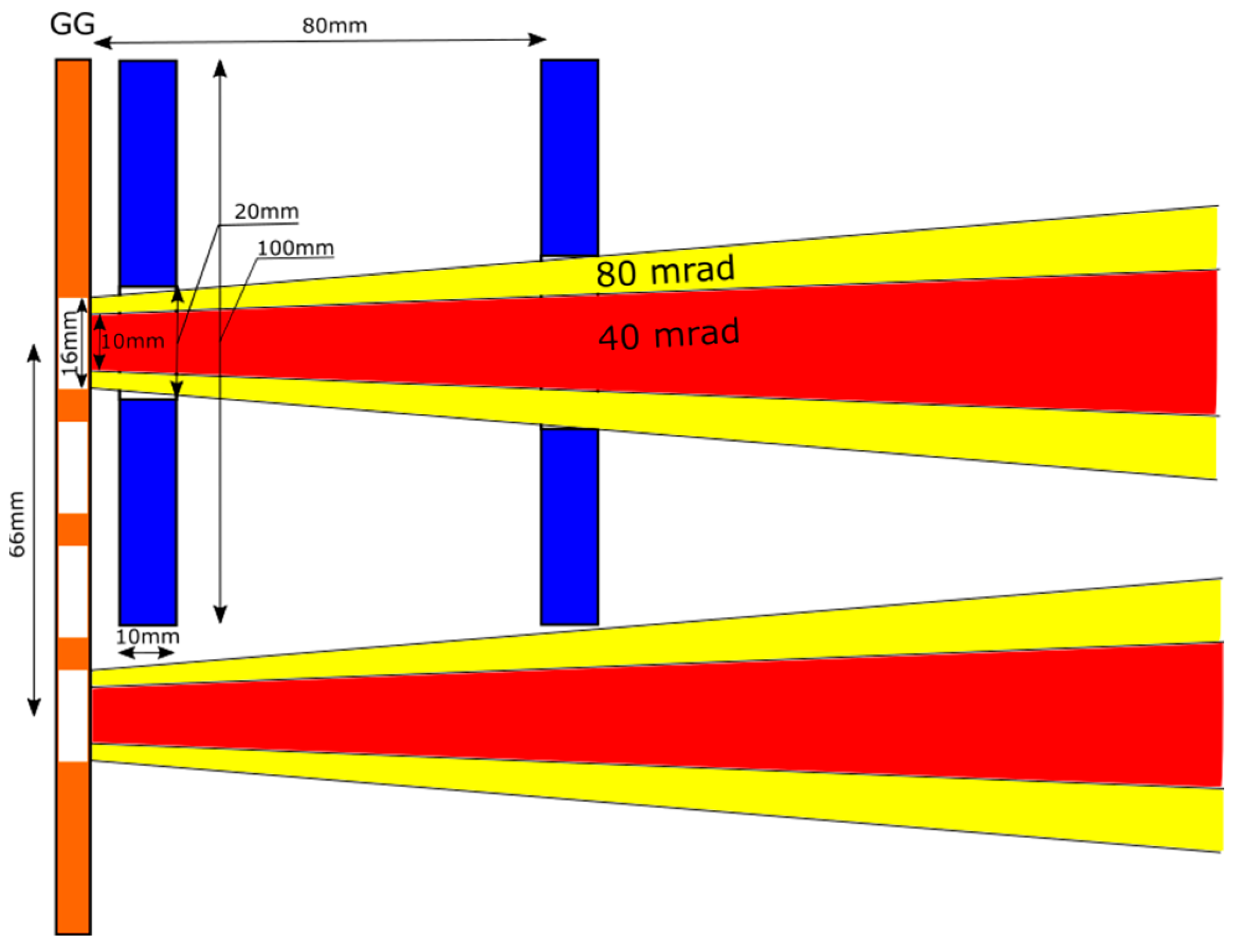
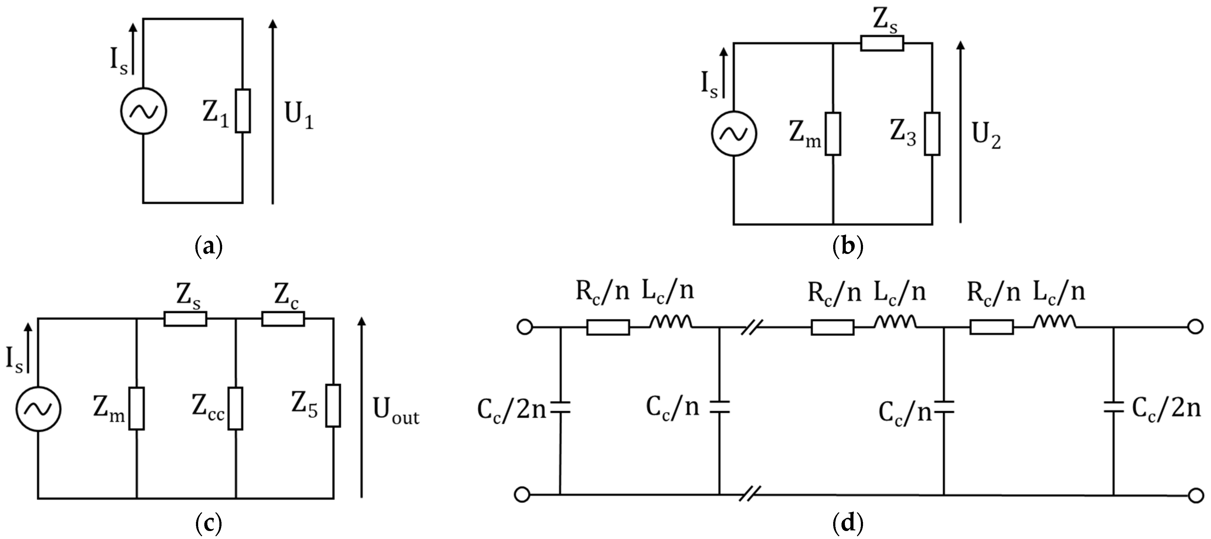
3. BCM Concept Design
4. Sensor R&D
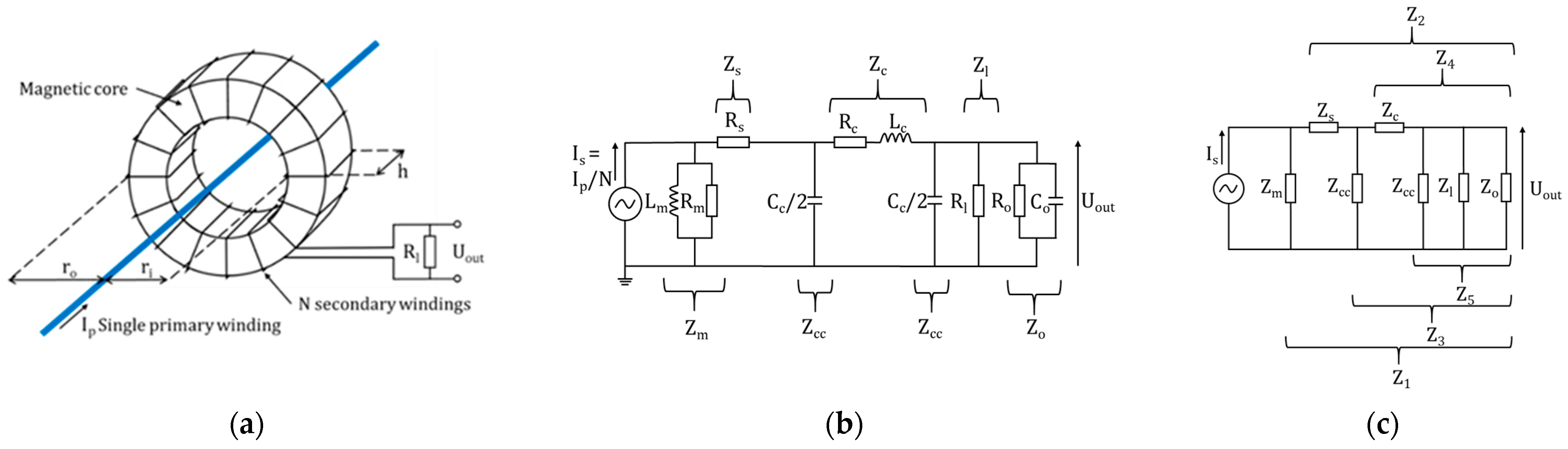
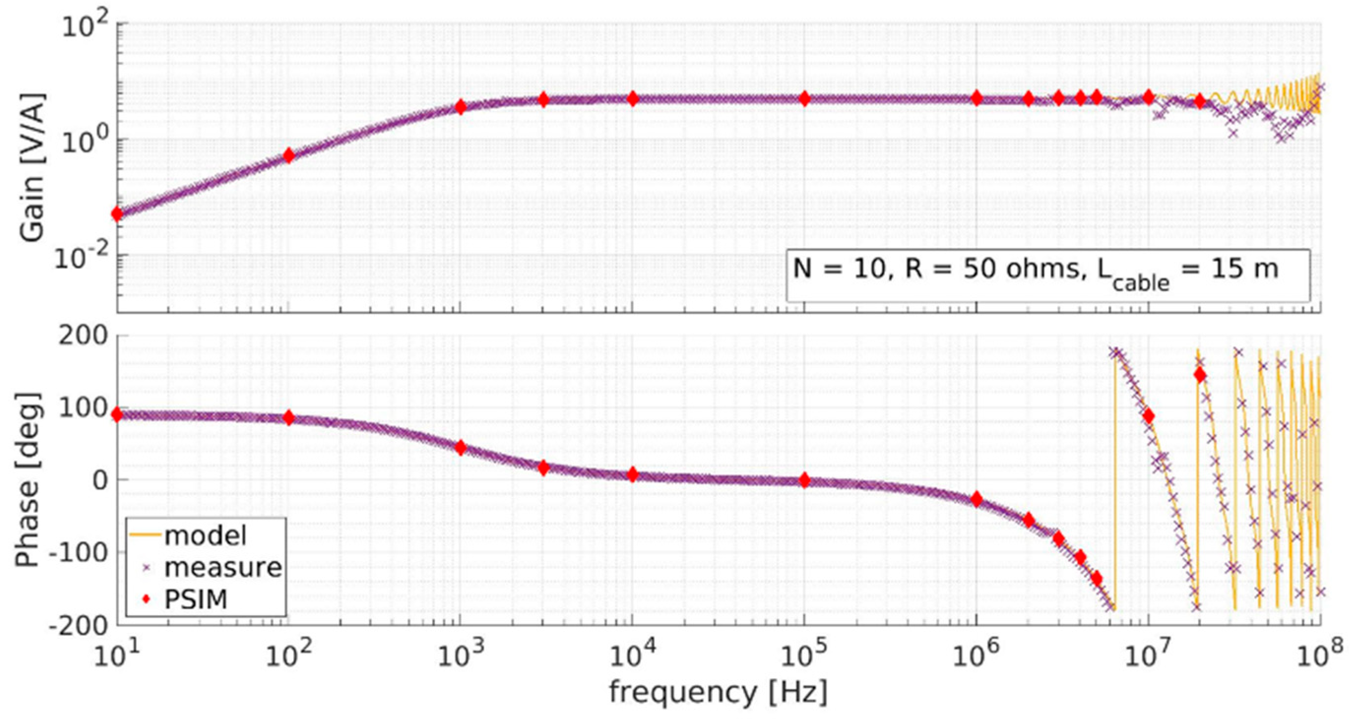
4.1. AC Sensors
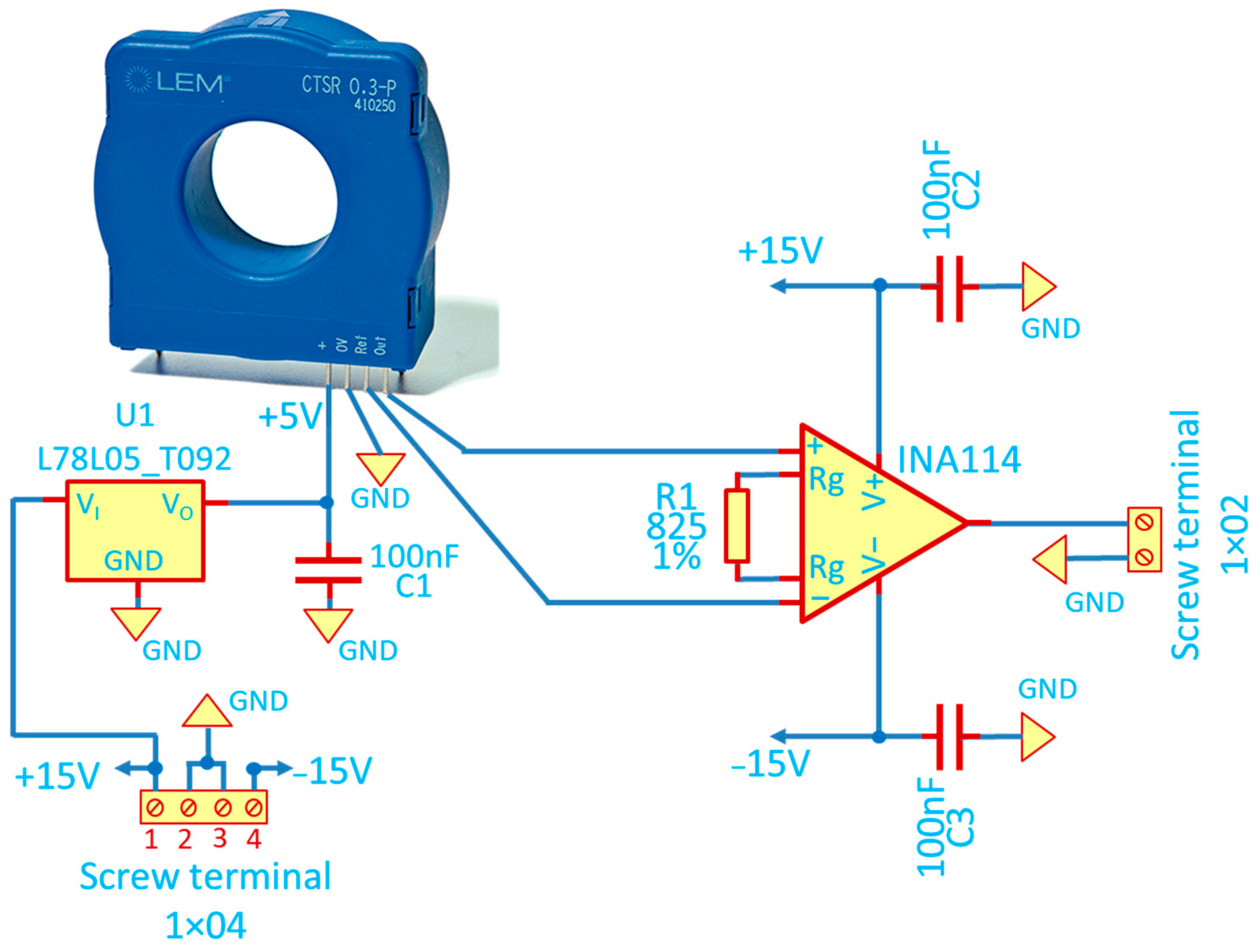
4.2. DC Sensors
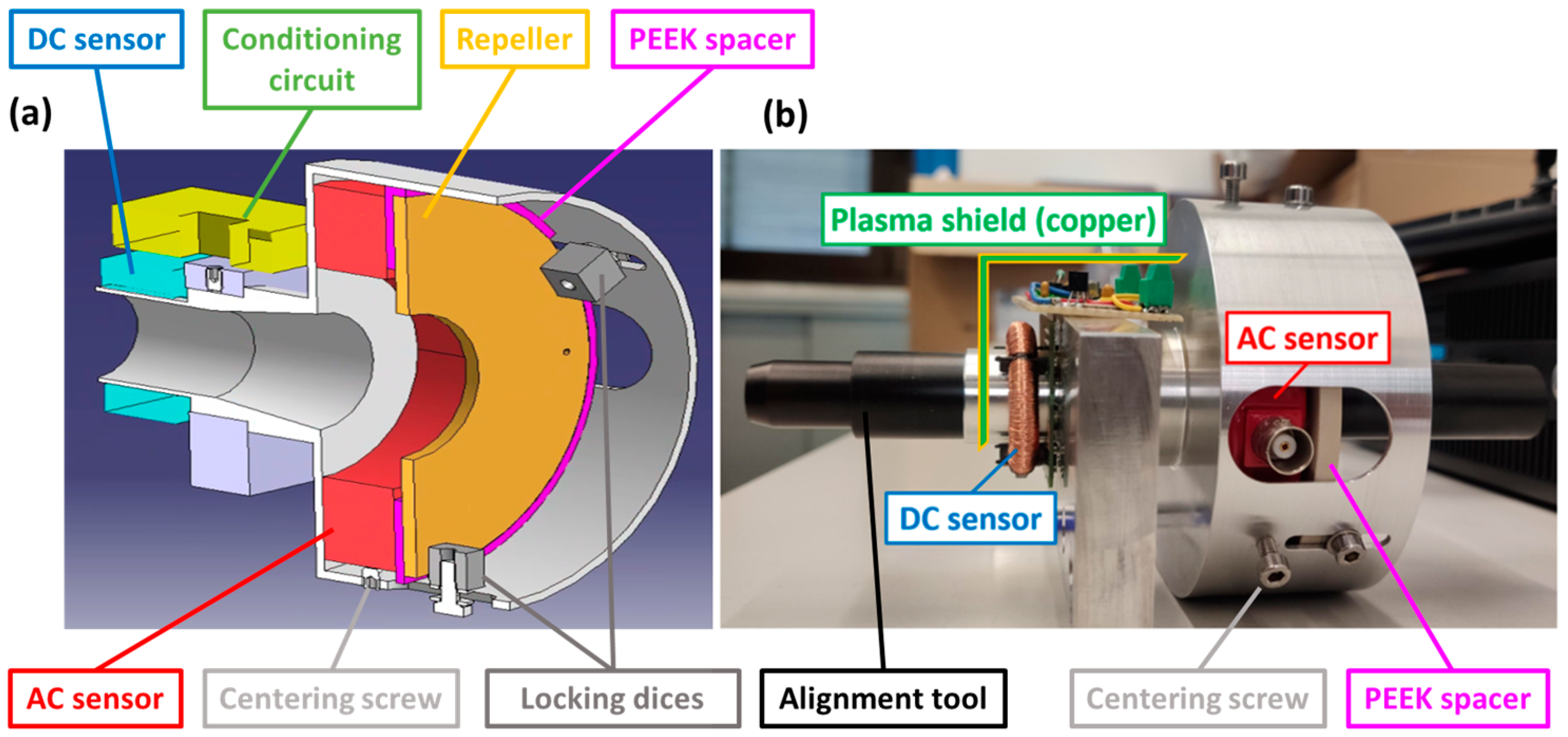
4.3. Mounting Structure
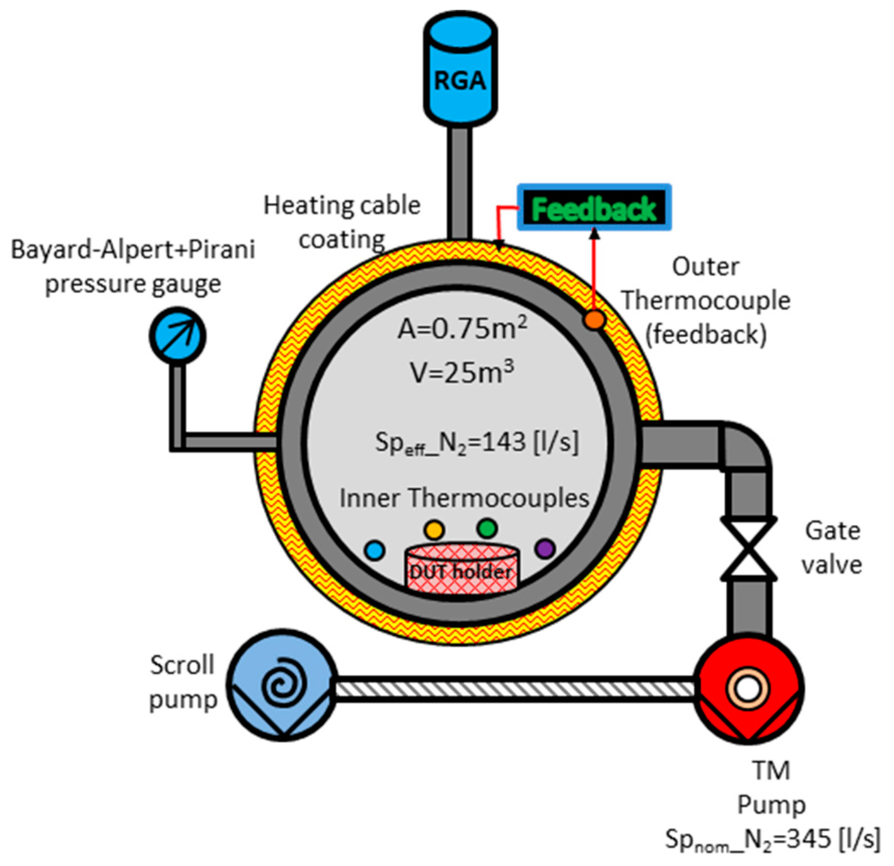
4.4. Vacuum Testing
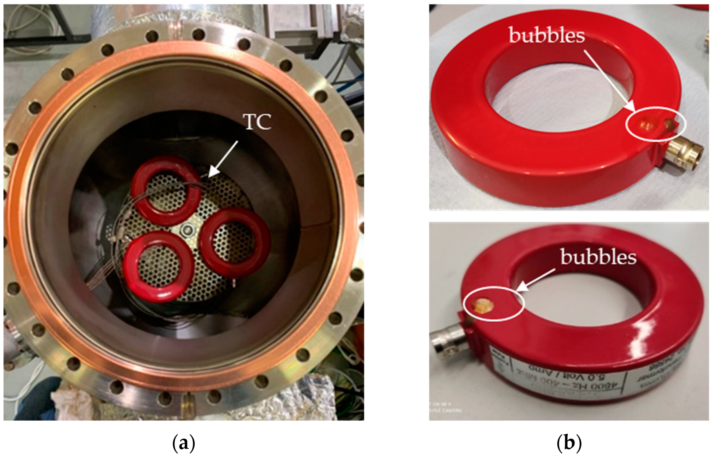
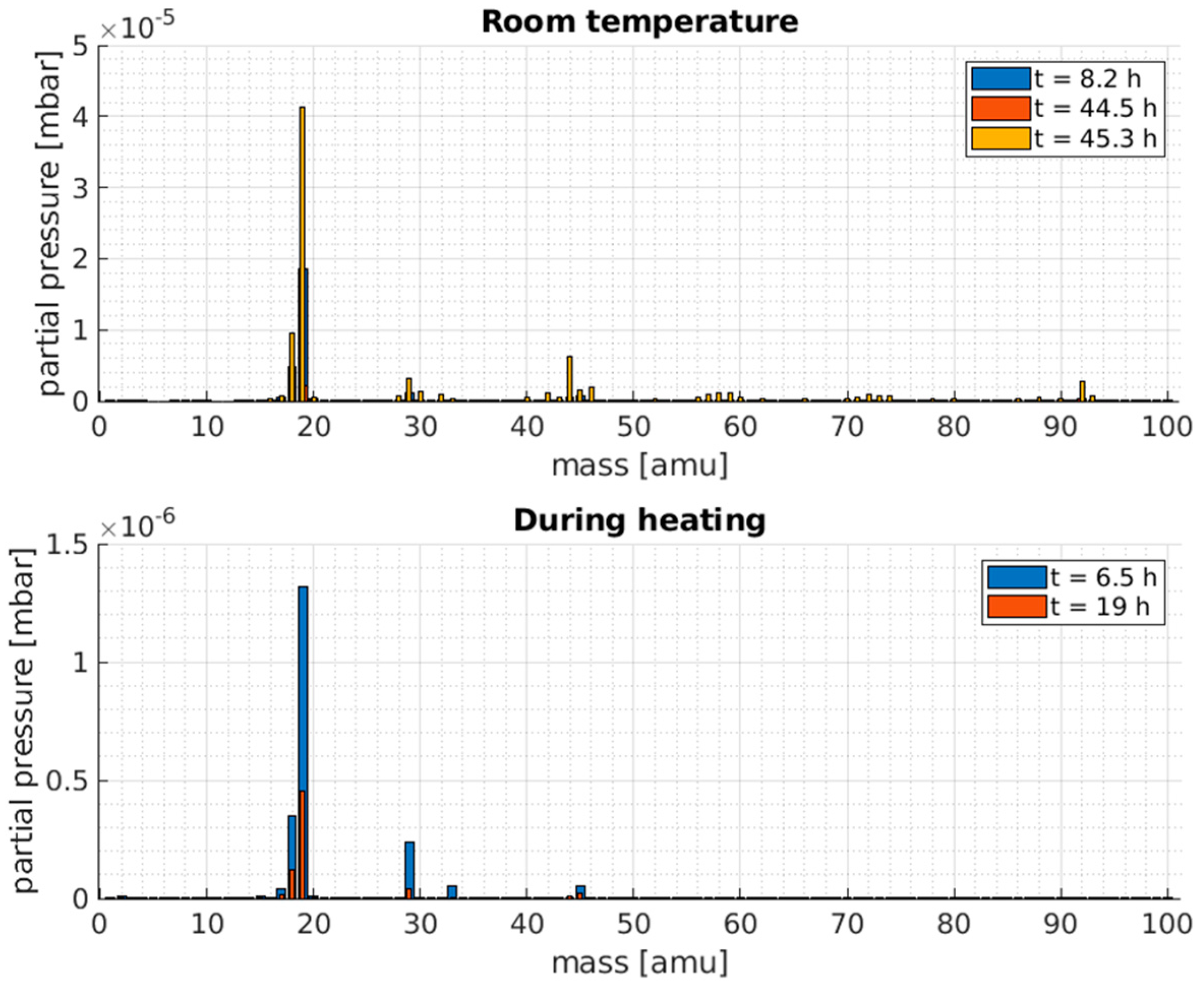
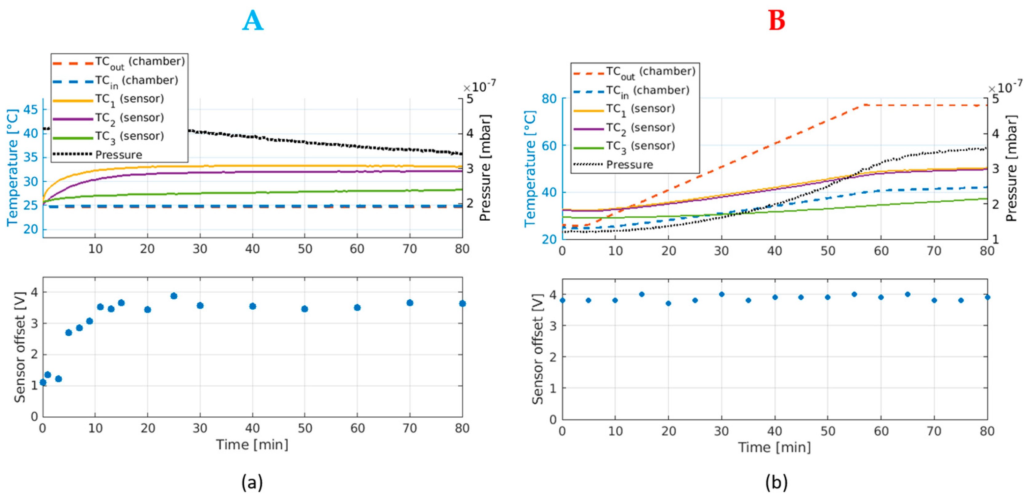
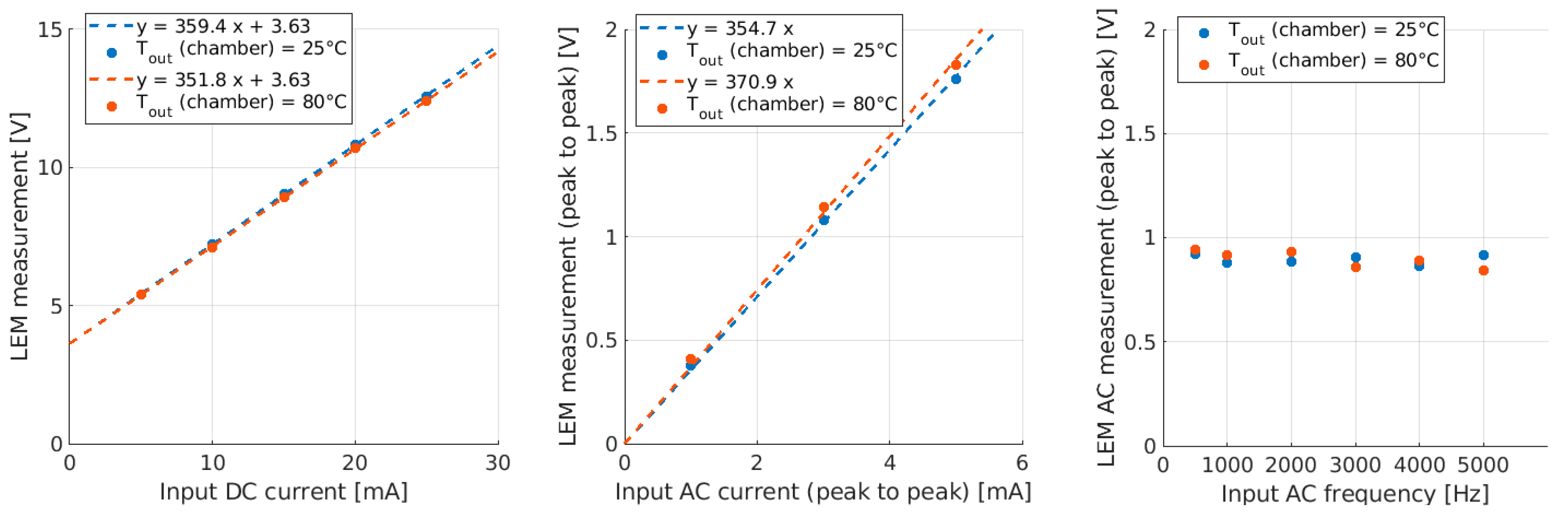
4.4.1. AC Sensor Outgassing Tests
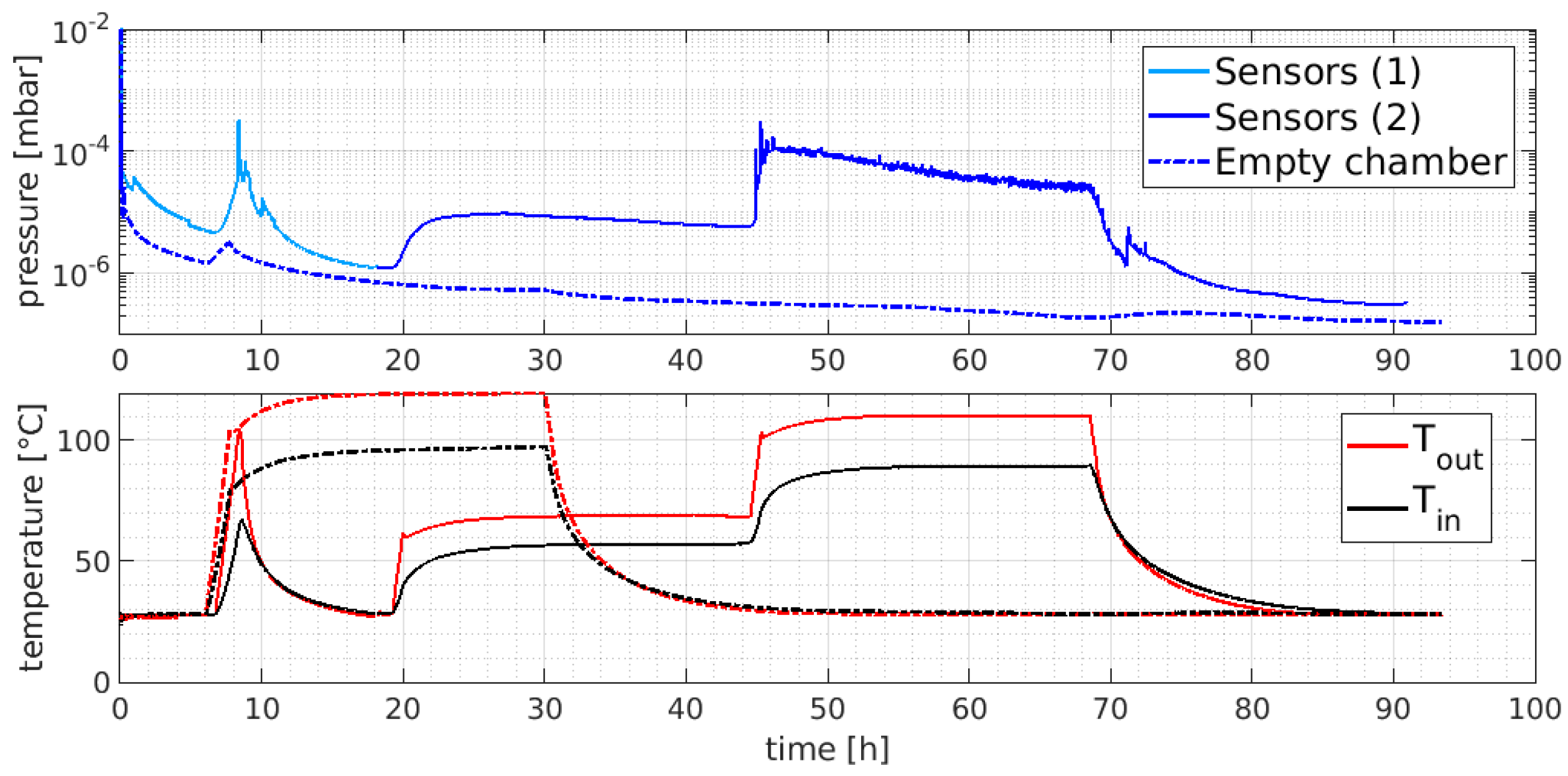
4.4.2. DC Sensor Vacuum Tests
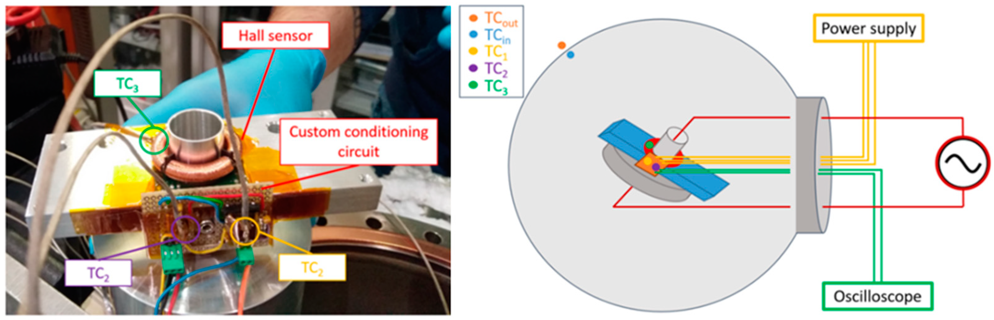
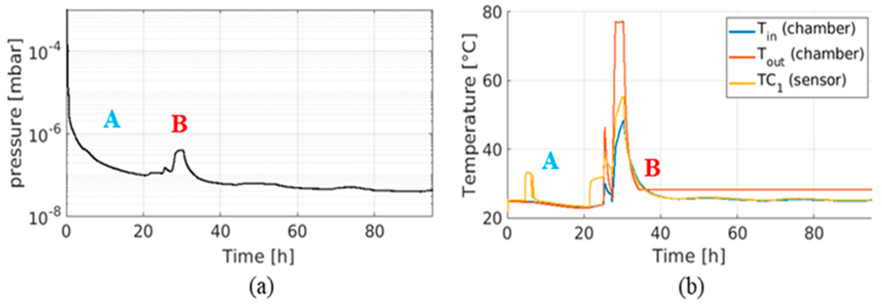
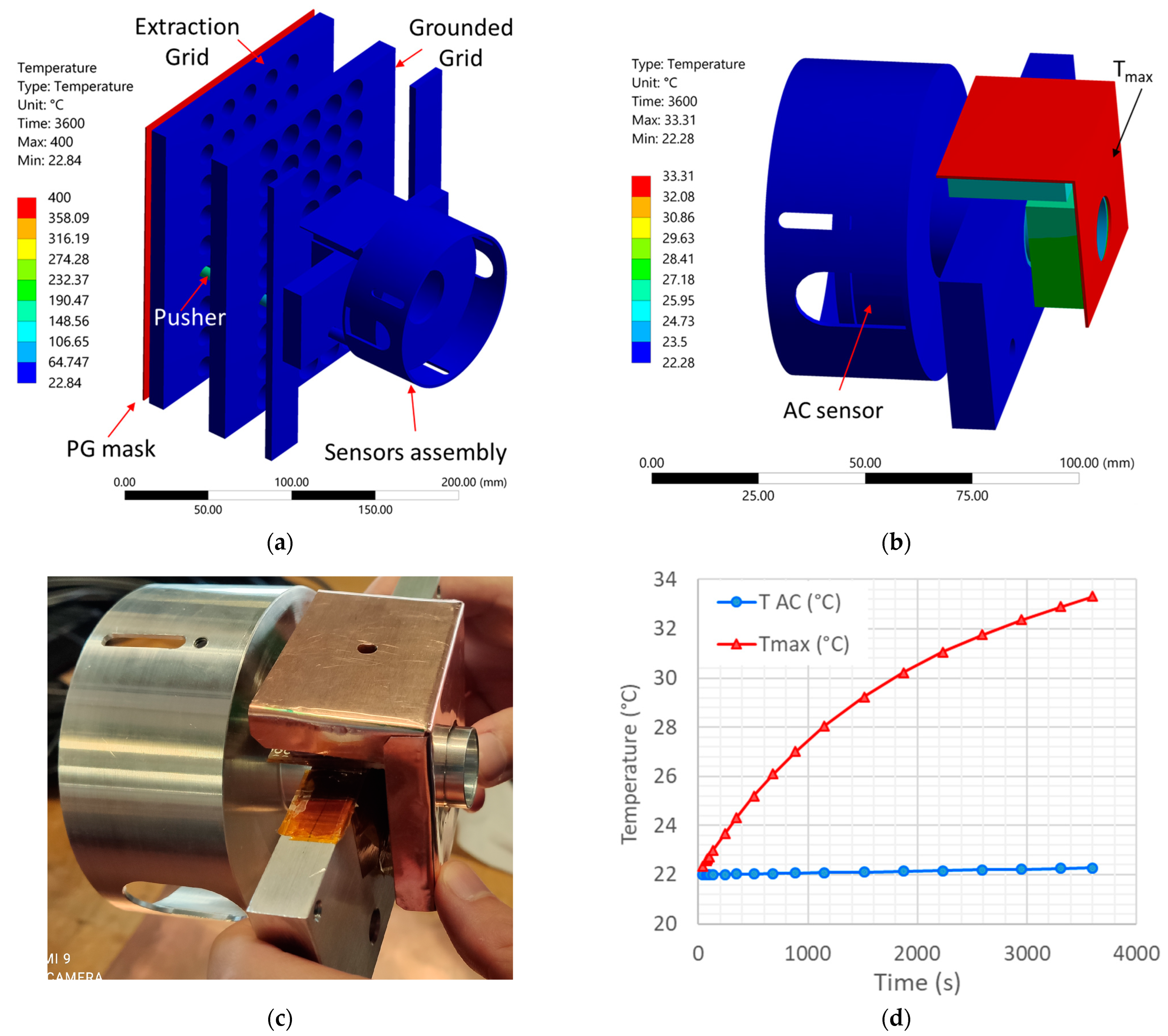
4.4.3. Thermal Simulations
- PG mask temperature set to 400 °C with emissivity equal to 1, representing the worst-case scenario (black body emitter, including a safety margin in the PG temperature);
- EG temperature set to 30 °C since it is actively cooled, and the emissivity of EG and GG set equal to 0.2 (slightly oxidized copper, the grids were exposed to air and humidity in the past [26]);
- Emissivity of pushers equal to 0.85 (pyrex glass [27]);
- Emissivity of the DC sensor and conditioning circuit equal to 0.75 (fiberglass of the electric circuit board [28]);
- Emissivity of plasma shield equal to 0.2 (slightly oxidized copper, the plate was exposed to air and humidity in the past [26]);
- Emissivity of sensors support structure equal to 0.1 (aluminum [27]);
- Emissivity of AC sensor equal to 0.03 (polished copper, the sensor surface was covered by copper tape to prevent plasma etching and to reduce the absorbed power by radiation [26]);
- Constant ambient temperature equal to 22 °C representing the vacuum vessel’s inner surface which is at room temperature.
5. Overview of the System
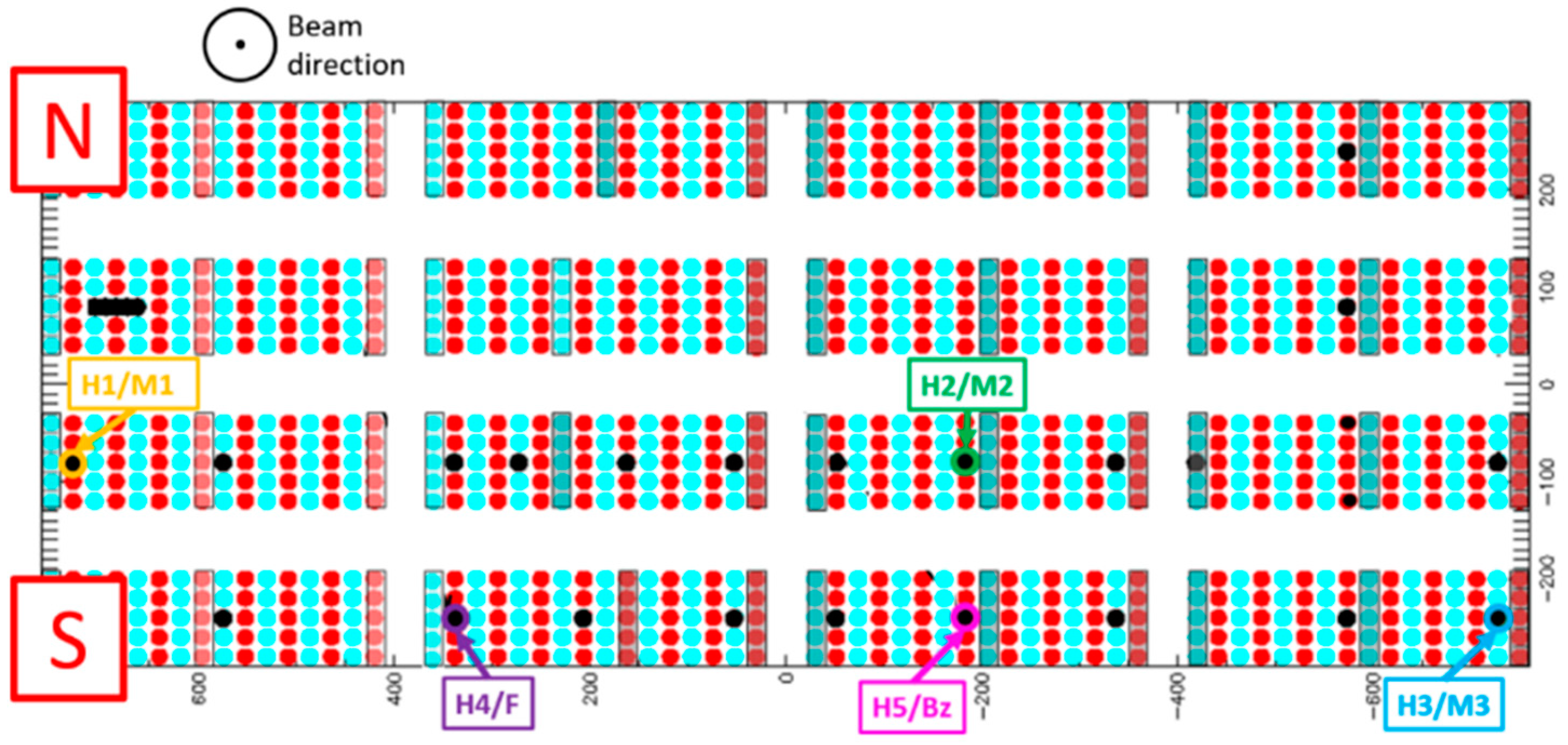
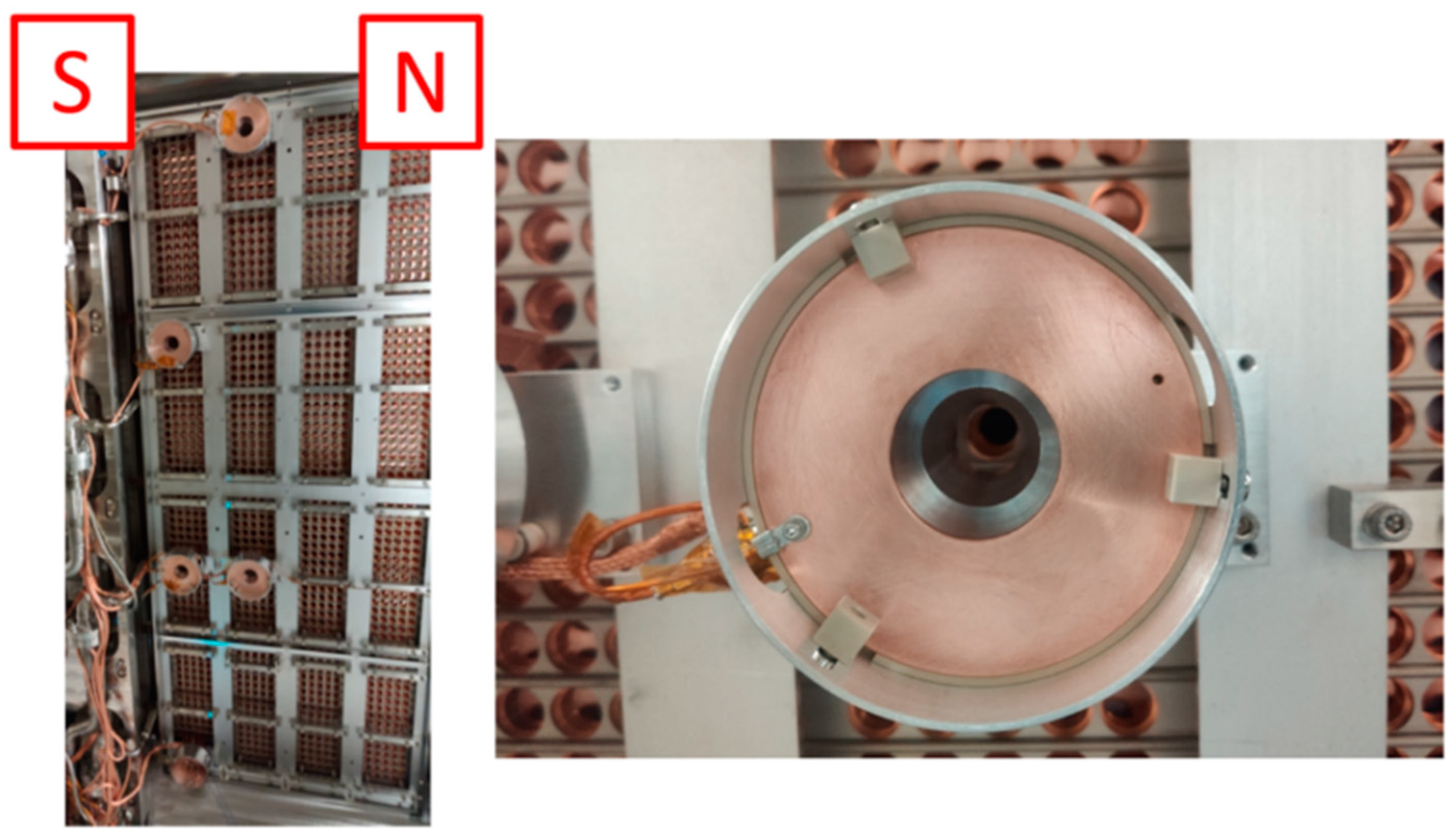
5.1. Sensor Installation
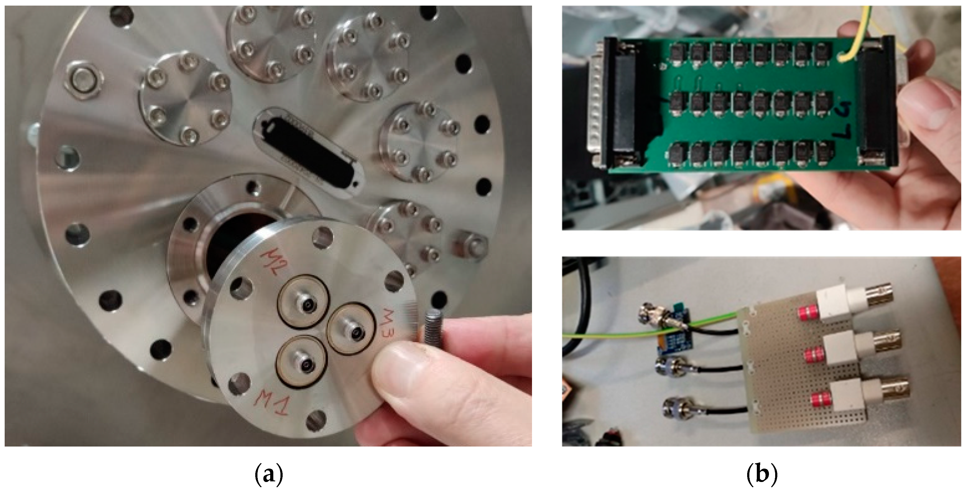
5.2. Feedthroughs and Surge Arresters
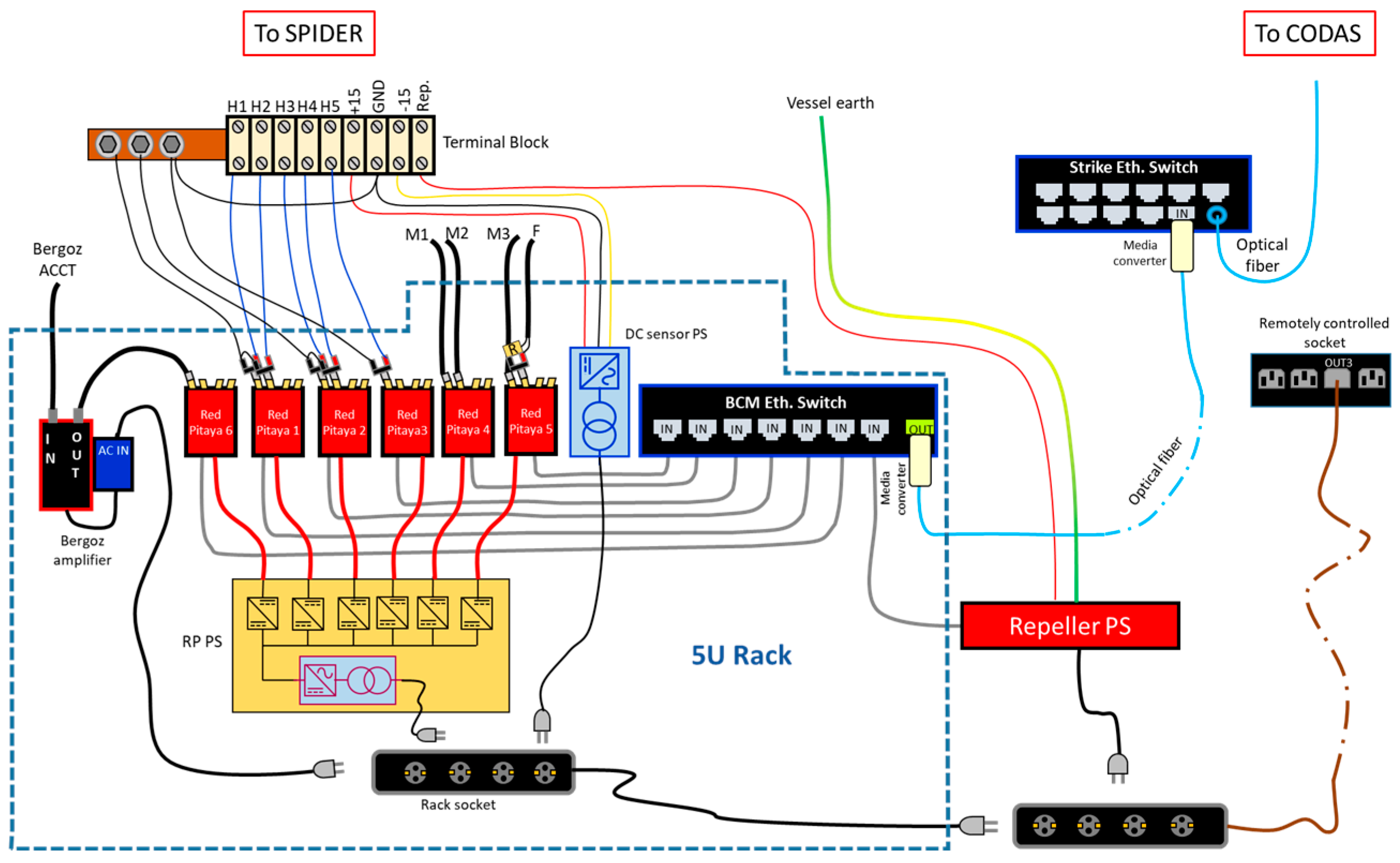
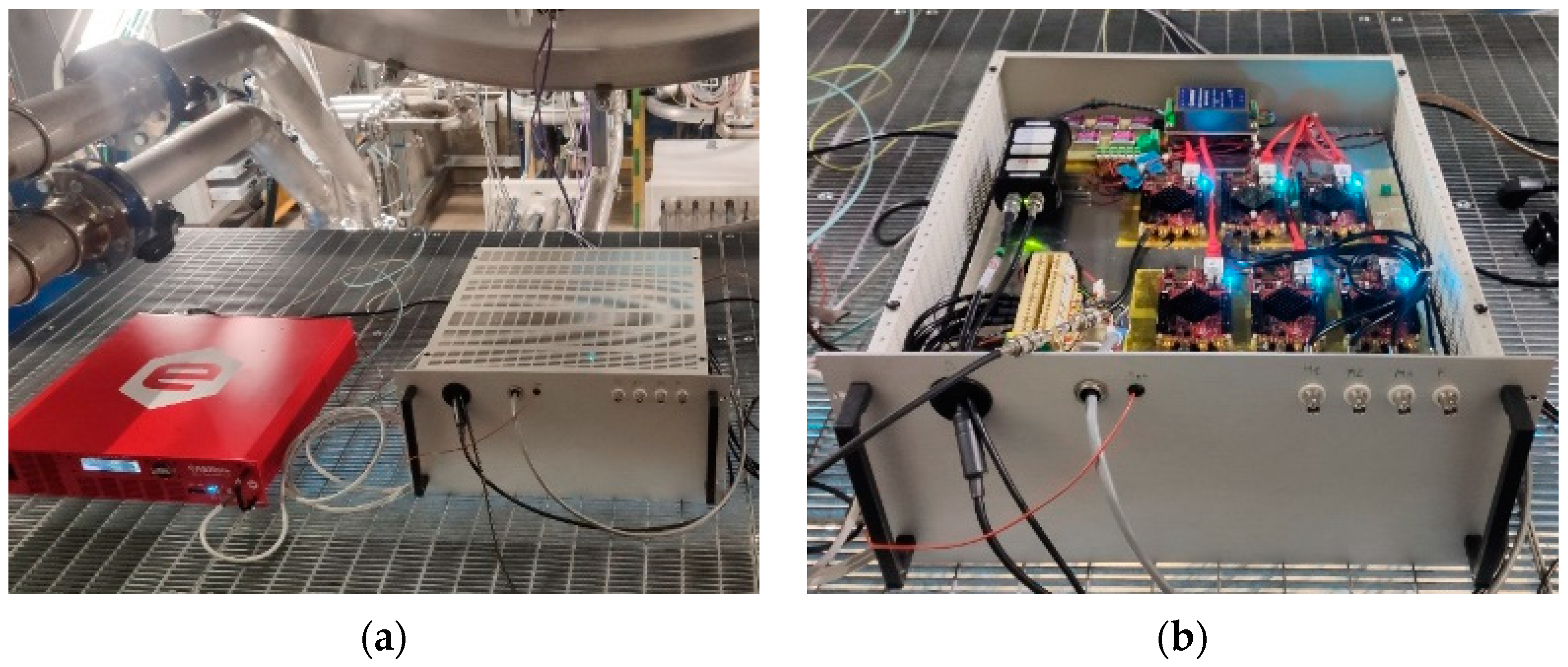
5.3. Data Acquisition and Power Supply System
5.4. CODAS
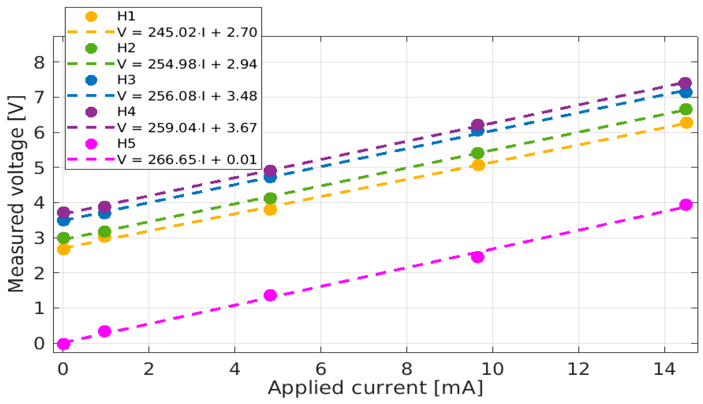
5.5. Calibration
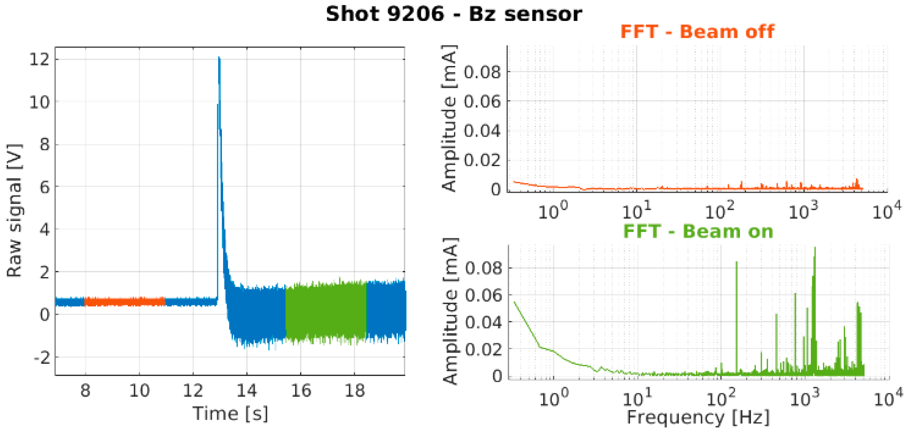
6. Experimental Results
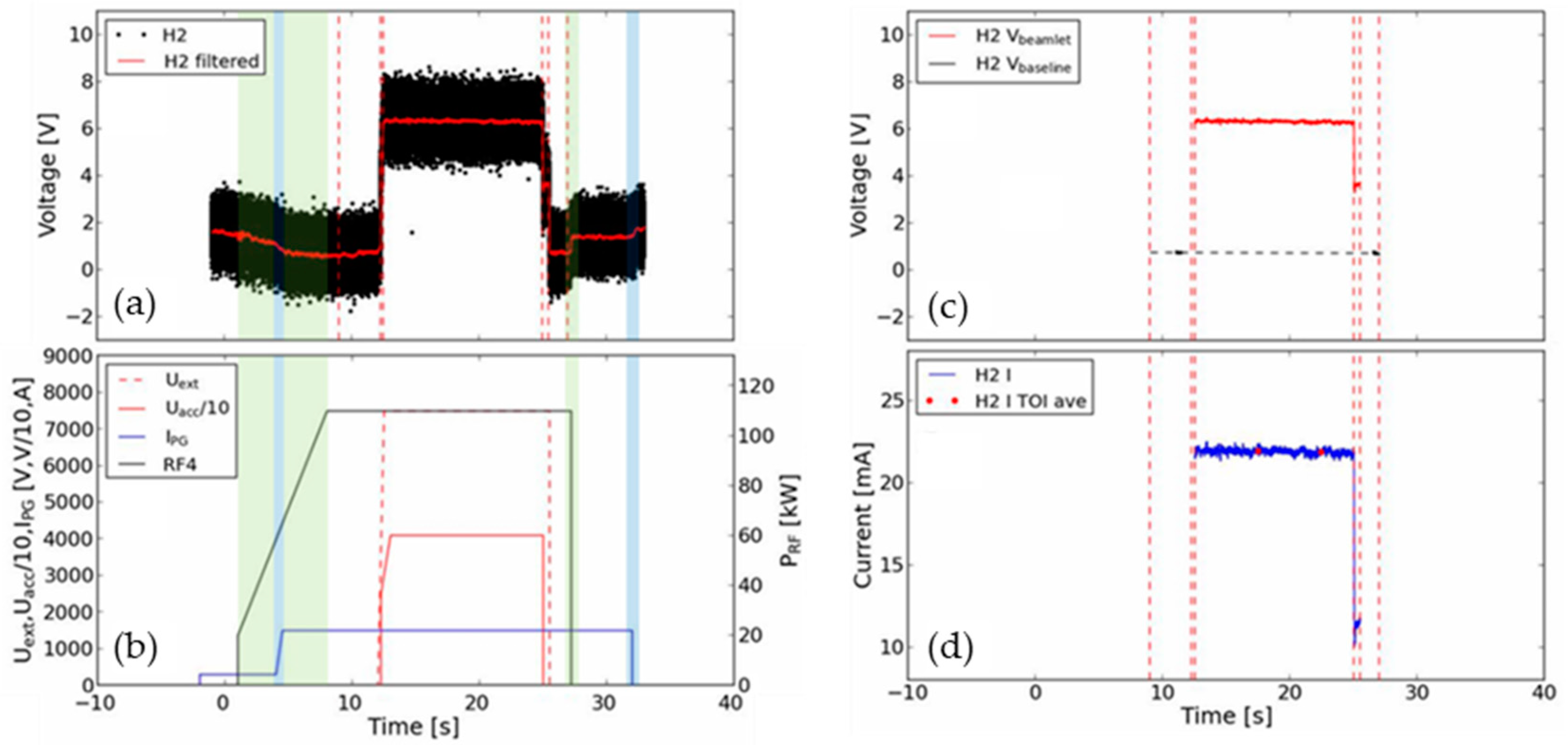
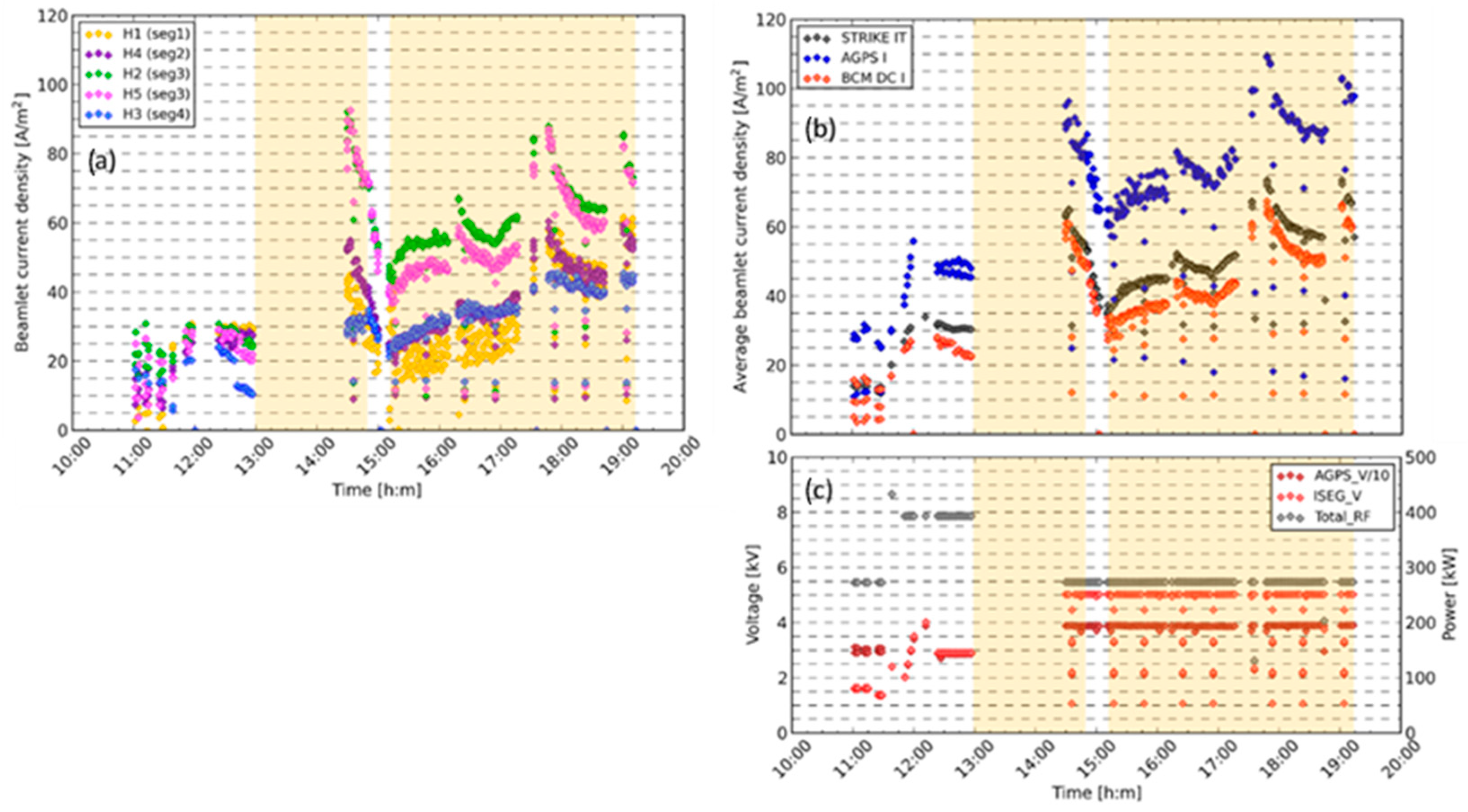
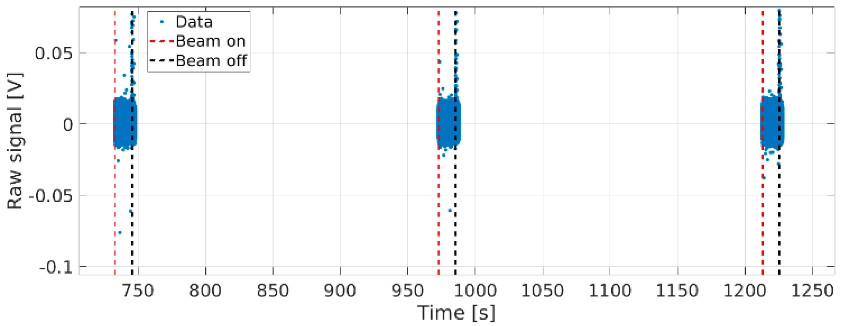
6.1. DC Results
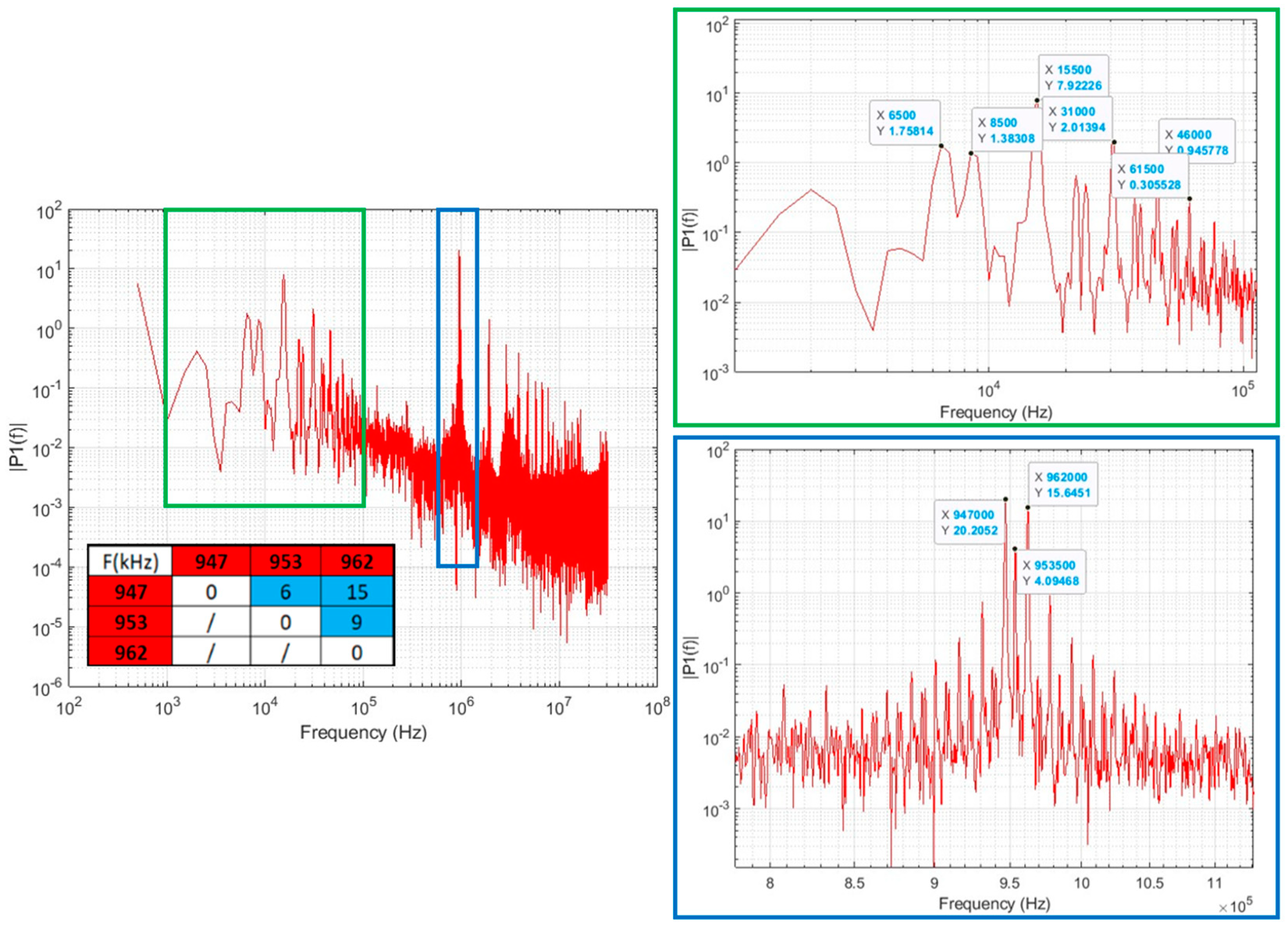
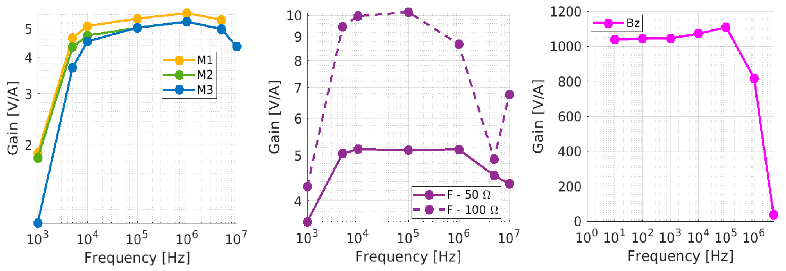
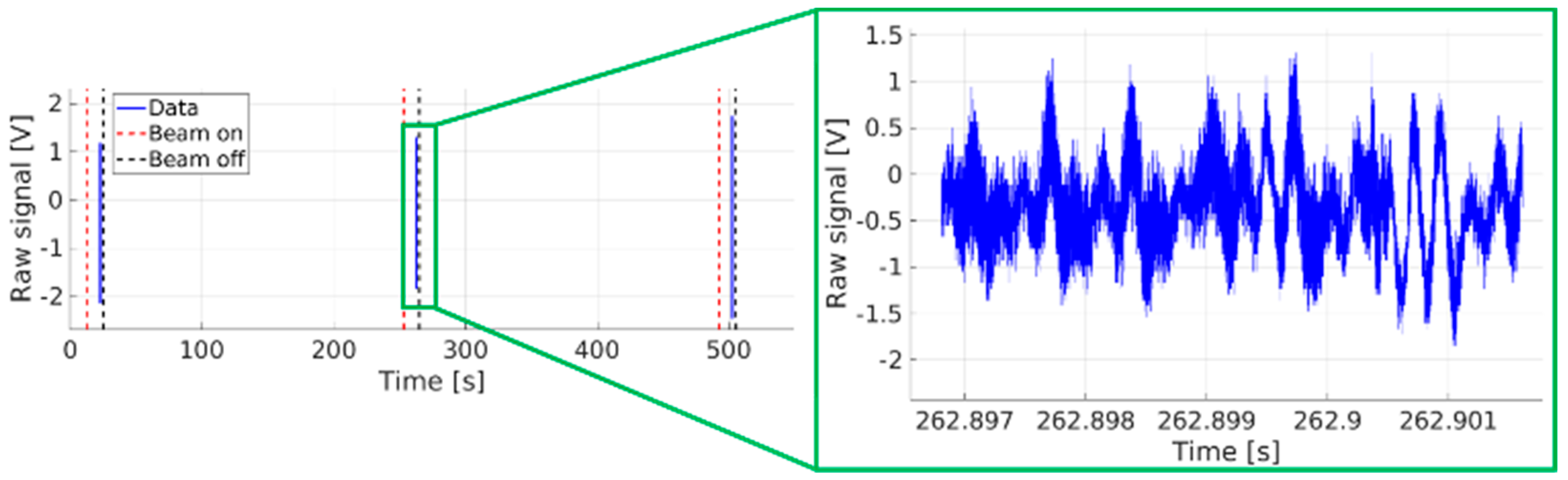
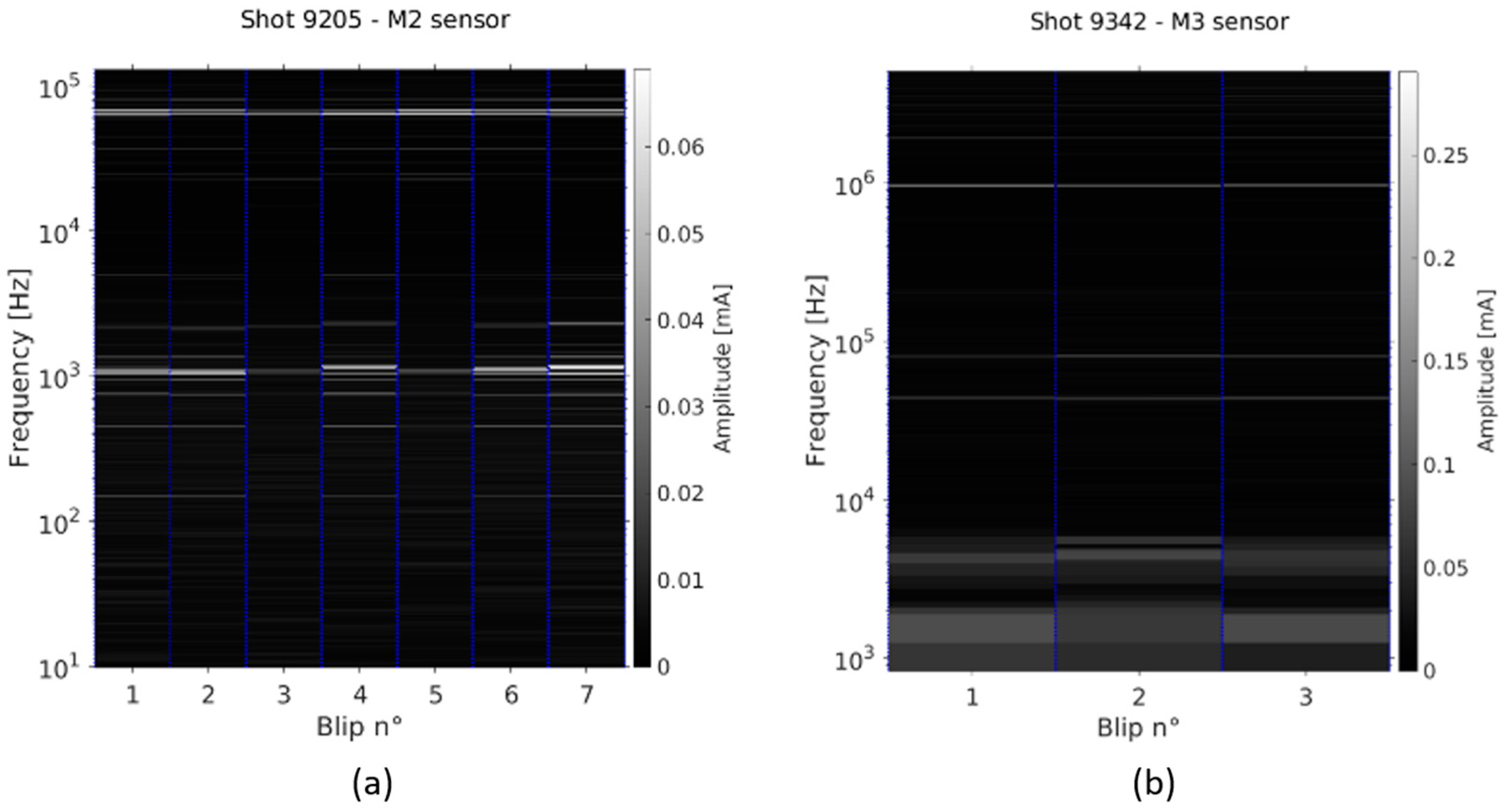
6.2. AC Results
7. Conclusions
Author Contributions
Funding
Institutional Review Board Statement
Informed Consent Statement
Data Availability Statement
Acknowledgments
Conflicts of Interest
Appendix A

References
- Serianni, G.; Toigo, V.; Bigi, M.; Boldrin, M.; Chitarin, G.; Del Bello, S.; Grando, L.; Luchetta, A.; Marcuzzi, D.; Pasqualotto, R. SPIDER in the roadmap of the ITER neutral beams. Fusion Eng. Des. 2019, 146, 2539. [Google Scholar] [CrossRef]
- Pimazzoni, A.; Brombin, M.; Canocchi, G.; Delogu, R.S.; Fasolo, D.; Franchin, L.; Laterza, B.; Pasqualotto, R.; Serianni, G.; Tollin, M. Assessment of the SPIDER beam features by diagnostic calorimetry and thermography. Rev. Sci. Instrum. 2020, 91, 033301. [Google Scholar] [CrossRef]
- Brown, I.G. The Physics and Technology of Ion Sources; Wiley: New York, NY, USA, 2004. [Google Scholar]
- Campbell, D.J. Preface to special topic: ITER. Phys. Plasmas 2015, 22, 021701. [Google Scholar] [CrossRef]
- Kuriyama, M.; Akino, N.; Ebisawa, N.; Grisham, L.; Liquen, H.; Honda, A.; Itoh, T.; Kawai, M.; Kazawa, M.; Mogaki, K.; et al. Development of negative-ion based NBI system for JT-60. J. Nucl. Sci. Technol. 1998, 35, 739–749. [Google Scholar] [CrossRef]
- Fantz, U.; Bonomo, F.; Fröschle, M.; Heinemann, B.; Hurlbatt, A.; Kraus, W.; Schiesko, L.; Nocentini, R.; Riedl, R.; Wimmer, C. Advanced NBI beam characterization capabilities at the recently improved test facility BATMAN Upgrade. Fusion Eng. Des. 2019, 146, 212–215. [Google Scholar] [CrossRef] [Green Version]
- Heinemann, B.; Fantz, U.; Franzen, P.; Froeschle, M.; Kircher, M.; Kraus, W.; Martens, C.; Nocentini, R.; Riedl, R.; Ruf, B.; et al. Negative ion test facility ELISE—Status and first results. Fusion Eng. Des. 2013, 88, 512–516. [Google Scholar] [CrossRef]
- Gasparini, F.; Recchia, M.; Bigi, M.; Patton, T.; Zamengo, A.; Gaio, E. Investigation on stable operational regions for SPIDER RF oscillators. Fusion Eng. Des. 2019, 146, 2172–2175. [Google Scholar] [CrossRef]
- Belchenko, Y.; Dimov, G.; Dudnikov, V. Powerful injector of neutrals with a surface-plasma source of negative ions. Nucl. Fusion 1974, 14, 113. [Google Scholar] [CrossRef]
- Serianni, G.; Toigo, V.; Bigi, M.; Boldrin, M.; Chitarin, G.; Bello, S.D.; Grando, L.; Luchetta, A.; Marcuzzi, D.; Tobari, H.; et al. First operation in SPIDER and the path to complete MITICA. Rev. Sci. Instrum. 2020, 91, 023510. [Google Scholar] [CrossRef] [PubMed] [Green Version]
- Pavei, M.; Bello, S.D.; Gambetta, G.; Maistrello, A.; Marcuzzi, D.; Pimazzoni, A.; Sartori, E.; Serianni, F.D.A.G.; Franchin, L.; Tollin, M. SPIDER plasma grid masking for reducing gas conductance and pressure in the vacuum vessel. Fusion Eng. Des. 2020, 161, 112036. [Google Scholar] [CrossRef]
- Candeloro, V.; Serianni, G.; Fadone, M.; Laterza, B.; Sartori, E. Development of a triple Langmuir probe for plasma characterization in SPIDER. IEEE Trans. Plasma Sci. 2022, 50, 3871–3876. [Google Scholar] [CrossRef]
- Shinto, K.; Shibata, T.; Miura, A.; Miyao, T.; Wada, M. Observation of beam current fluctuation extracted from an RF-driven H-ion source. AIP Conf. Proc. 2018, 2011, 080016. [Google Scholar]
- Wada, M.; Shinto, K.; Shibata, T.; Sasao, M. Measurement of a time dependent spatial beam profile of an RF-driven H− ion source. Rev. Sci. Instrum. 2020, 91, 013330. [Google Scholar] [CrossRef]
- Veltri, P.; Cavenago, M.; Serianni, G. Spatial characterization of the space charge compensation of negative ion beams. AIP Conf. Proc. 2013, 1515, 541–548. [Google Scholar]
- Bergoz Instrumentation Products Website. Available online: https://www.bergoz.com/products/acct/ (accessed on 22 June 2023).
- MagneLab CT Current Transformer Webpage. Available online: https://gmw.com/product/ct/ (accessed on 22 June 2023).
- Unser, K.B. Toroidal AC and DC current transformers for beam intensity measurements. Atomkernenerg. Kerntech. 1985, 47, 48–52. [Google Scholar]
- Webber, R.C. Charged particle beam current monitoring tutorial. In Proceedings of the Beam Instrumentation Workshop, Vancouver, BC, Canada, 3–6 October 1994. [Google Scholar]
- Zachariades, C.; Shuttleworth, R.; Giussani, R.; MacKinlay, R. Optimization of a high-frequency current transformer sensor for partial discharge detection using finite-element analysis. IEEE Sens. J. 2016, 16, 7526–7533. [Google Scholar] [CrossRef] [Green Version]
- Fuzernova, J.; Fuzer, J.; Kollar, P.; Bures, R.; Faberova, M.J. Complex permeability and core loss of soft magnetic Fe-based nanocrystalline powder cores. J. Magn. Magn. Mater. 2013, 345, 77–81. [Google Scholar] [CrossRef]
- Nanocrystalline VITROPERM ECM Products. Available online: https://www.mouser.com/pdfdocs/VACChokesandCoresDatasheet.pdf (accessed on 22 June 2023).
- Vacuumshmelze Nanocrystalline VITROPERM. Available online: https://vacuumschmelze.com/products/soft-magnetic-materials-and-stamped-parts/nanocrystalline-material-vitroperm (accessed on 22 June 2023).
- LEM CTSR 0.3-P Webpage. Available online: https://www.lem.com/en/ctsr-03p (accessed on 23 June 2023).
- Tumanski, S. Modern Magnetic Field Sensors—A Review. Organ 2013, 10, 1–12. [Google Scholar]
- Fluke Process Instruments–Metal Emissivities. Available online: https://www.flukeprocessinstruments.com/en-us/service-and-support/knowledge-center/infrared-technology/emissivity-metals (accessed on 22 June 2023).
- The Engineering Toolbox–Surface Emissivity Coefficients. Available online: https://www.engineeringtoolbox.com/emissivity-coefficients-d_447.html (accessed on 26 June 2023).
- Thermoworks–Infrared Emissivity Table. Available online: https://www.thermoworks.com/emissivity-table/ (accessed on 26 June 2023).
- Luchetta, A.; Manduchi, G.; Taliercio, C. SPIDER CODAS Evolution toward the ITER compliant neutral beam injector CODAS. IEEE Trans. Nucl. Sci. 2017, 64, 2765–2769. [Google Scholar] [CrossRef]
- Ardley, T. First Principles of a Gas Discharge Tube (GDT) Primary Protector—Rev 2; Bourns: Altadena, CA, USA, 2008. [Google Scholar]
- Garola, A.R.; Manduchi, G.; Gottardo, M.; Cavazzana, R.; Recchia, M.; Taliercio, C.; Luchetta, A. A Zynq-Based Flexible ADC Architecture Combining Real-Time Data Streaming and Transient Recording. IEEE Trans. Nucl. Sci. 2020, 68, 245–249. [Google Scholar] [CrossRef]
- Shepherd, A.; Duteil, B.P.; Patton, T.; Pimazzoni, A.; Garola, A.R.; Sartori, E.; Serianni, G. Initial results from the SPIDER beamlet current diagnostic. IEEE Trans. Plasma Sci. 2022, 50, 3906–3912. [Google Scholar] [CrossRef]
- Shepherd, A.; Patton, T.; Duteil, B.P.; Pimazzoni, A.; Garola, A.R.; Sartori, E. Beam homogeneity of caesium seeded SPIDER using a direct beamlet current measurement. Fusion Eng. Des. 2023, 192, 113599. [Google Scholar] [CrossRef]
- Shepherd, A.; Patton, T.; Duteil, B.P.A.P.; Garola, A.R.; Sartori, E.; Ugoletti, M.; Serianni, G. Direct current measurements of the SPIDER beam: A comparison to existing beam diagnostics. arXiv 2023, arXiv:2305.18001. [Google Scholar]
- Duteil, B.P.; Shepherd, A.; Patton, T.; Garola, A.R.; Casagrande, R. First characterization of the SPIDER beam AC component with the Beamlet Current Monitor. Fusion Eng. Des. 2023, 190, 113529. [Google Scholar] [CrossRef]


| Requirements | Value | Note |
|---|---|---|
| Current full-scale | ≥40 mA | Max beamlet current Ib for the nominal accelerated D-current of 50 A |
| Current resolution | ≤1 mA | Max allowed beam non-uniformity for Ib = 10 mA (early phase of surface production operation) |
| Sensitivity | ≥5 mV/mA | Typical ADC sensitivity considering noise |
| Bandwidth | DC-10 MHz | Beatings in the kHz range and MHz harmonics due to RF |
| Clearance | ≥20 mm | Beamlet cross-section at GG, divergence and deflection |
| External diameter | 100 mm | Minimum distance between adjacent beamlets, divergence |
| Repeller voltage | ≥100 V | STRIKE potential |
| CT Parameter | Value |
|---|---|
| ri [m] | 0.03 |
| ro [m] | 0.045 |
| h [m] | 0.02 |
| N | 10 |
| μr | 50,000 |
| Rs [Ω] | 0.22 |
| Rc [Ω/m] | 0.048 |
| Lc [nH/m] | 250 |
| Cc [pF/m] | 100 |
| Lc [m] | 15 |
| Rl [Ω] | 50 |
| Ro [MΩ] | 1 |
| Co [pF] | 50 |
| K [V/A] | 4.9 |
| flow (−3 dB) [Hz] | 1000 |
Disclaimer/Publisher’s Note: The statements, opinions and data contained in all publications are solely those of the individual author(s) and contributor(s) and not of MDPI and/or the editor(s). MDPI and/or the editor(s) disclaim responsibility for any injury to people or property resulting from any ideas, methods, instructions or products referred to in the content. |
© 2023 by the authors. Licensee MDPI, Basel, Switzerland. This article is an open access article distributed under the terms and conditions of the Creative Commons Attribution (CC BY) license (https://creativecommons.org/licenses/by/4.0/).
Share and Cite
Patton, T.; Shepherd, A.; Pouradier Duteil, B.; Rigoni Garola, A.; Brombin, M.; Candeloro, V.; Manduchi, G.; Pavei, M.; Pasqualotto, R.; Pimazzoni, A.; et al. Design and Development of a Diagnostic System for a Non-Intercepting Direct Measure of the SPIDER Ion Source Beamlet Current. Sensors 2023, 23, 6211. https://doi.org/10.3390/s23136211
Patton T, Shepherd A, Pouradier Duteil B, Rigoni Garola A, Brombin M, Candeloro V, Manduchi G, Pavei M, Pasqualotto R, Pimazzoni A, et al. Design and Development of a Diagnostic System for a Non-Intercepting Direct Measure of the SPIDER Ion Source Beamlet Current. Sensors. 2023; 23(13):6211. https://doi.org/10.3390/s23136211
Chicago/Turabian StylePatton, Tommaso, Alastair Shepherd, Basile Pouradier Duteil, Andrea Rigoni Garola, Matteo Brombin, Valeria Candeloro, Gabriele Manduchi, Mauro Pavei, Roberto Pasqualotto, Antonio Pimazzoni, and et al. 2023. "Design and Development of a Diagnostic System for a Non-Intercepting Direct Measure of the SPIDER Ion Source Beamlet Current" Sensors 23, no. 13: 6211. https://doi.org/10.3390/s23136211