PCI Express Primer #1: Overview and Physical Layer
Simon Southwell
Semi-retired logic, software and systems designer. Technical writer, mentor, educator and presenter.
Introduction
This is the first in a set of articles giving an overview of the PCI Express (PCIe) protocol. This is quite a large subject and, I think, has the need to be split over a number of separate, more manageable documents and, even so, it is just a brief introduction to the subject. The main intended audience for these articles is anyone wishing to understand PCIe more if, say, they are working on a system which includes this protocol, or needs a primer before diving more deeply into the specifications themselves.
In this, the first article, an overview will be given of the PCIe architecture and an introduction to the first of three layers that make up the PCIe protocol. The Transaction and Data Link Layer details protocols will wait for future articles, and just the Physical Layer will be focused on here, after the overview.
To accompanying these articles a behavioural PCIe simulation model (pcievhost) written for Verilog is available. This runs a C model of the PCIe protocol on a simulation virtual processor (VProc) that interfaces this model to the Verilog environment. The model’s documentation explains how this is set up, and the API of the model for generating PCIe traffic. In these articles I will be making reference to the output of this model for many of the examples, but the model is also intended to allow readers the chance to explore the protocol for themselves. An example test environment is included which contains generating most traffic that the model is capable of producing and the reader is encouraged to get the model and make changes to the driving code to explore the PCIe space.
So, let’s start at the beginning.
Beginnings
Back when the PCI Express (PCIe) protocol was first published (at version 1.0a), it was decided that the HPC systems we were designing would upgrade from PCI to this new protocol so that we had a future path of bandwidth capability. There were a few 3rd party IP options at that time but, on inspection, these did not meet certain requirements for our designs, such as low latency through the interface. Therefore, I was tasked, amongst other things, to design a 16-lane endpoint interface to the PCIe specification that also met the other requirements. So, I got hold of the specification and started to look though it—all 500 plus pages of it. This was, of course, quite intimidating. I also went to a PCIe convention in London and spoke to one of the keynote speakers who lead a team that had implemented a PCIe interface. I asked her how long it took and how big a team she had. She replied that it took about a year, with a team of 4 engineers—oh, and she had 20 contractors doing various things, particularly on the verification side. I had 18 months and it was just me. One deep breath later I started breaking down the specification into the areas I would need to cover, optional things I could (at least at first) drop and slowly a pattern emerged that was a set of manageable concepts. In the end a working endpoint was implemented that covered the 1.1 specification with 16 lanes, or the 2.0 specification a with 8 lanes.
In these articles I want to introduce the concepts I learnt in that endpoint implementation exercise in the same manageable chunks. Since then, the 2.0 endpoint the specification has moved forward and, as at the time of writing, is at version 6.0. None-the-less, the article will start at the beginning before reviewing the changes that have taken place since the initial specification. Often systems can seem too complicated to understand because there have been a multitude of incremental changes and improvements to produce something of complexity. By starting at the beginning and then tracking the changes the problem becomes easier to follow, so that’s what I will do here.
PCIe Overview
Unlike its predecessor, PCI, PCIe is not a bus. It is a point-to-point protocol, more like AXI for example. The structure of the PCIe system consists of a number of point-to-point interfaces, with multiple peripherals and modules connected through an infrastructure, or fabric. An example fabric topology is shown below:

Unlike some other point-to-point architectures, there is a definite directional hierarchy with PCIe. The main CPU (or processor sub-system) sits at the top and is connected to a ‘root complex’ (RC) using whatever appropriate user interface. This root complex is the top level PCIe interconnect component and would typically be connected to main memory through which the CPU system would access it. The root complex will have a number of PCIe interfaces included, but to a limited degree. To expand the number of supported peripherals ‘switches’ may be attached to a root complex PCIe interface to expand the number of connections. Indeed, a switch may have one or more of its interfaces connected to other switches to allow even more expansion. Eventually an ‘endpoint’ (EP) is connected to an interface, which would be on a peripheral device, such as a graphics card or ethernet network card etc.
At each link, then, there is a definite ‘downstream’ link (from an upstream component e.g., RC to a switch or EP) and a ‘upstream’ link (from a downstream component e.g., EP to switch/RC). For each link the specification defines three layers built on top of each other
- Physical Layer
- Data Link Layer
- Transaction Layer
The physical layer is concerned with the electrical connections, the serialisation, encoding of bytes, the link initialisation and training and moving between power states. The data link layer sits on top of the physical layer and is involved in data flow control, ACK and NAK replies for transactions and power management. The transaction layer sits on top of the data link layer and is involved with sending data packet reads and writes for memory or I/O and returning read completions. The transaction layer also has a configuration space—a set of control and status registers separate to the main address map—and the transaction layer protocol has read and write packets to access this space.
Physical Layer
Lanes
The PCIe protocol communicates data through a set of serial ‘lanes’. Electrically, these are a pair of AC coupled differential wires. The number of lanes for an interface can be of differing widths, with x1, x2, x4, x8, x12, x16 and x32 supported. Obviously the higher the number of lanes the greater the data bandwidth that can be supported. Graphics cards, for instance, might be x16, whilst a serial interface might be x1. However, an interface need not be connected to another interface of the same size. During initialisation, active lanes are detected, and a negotiated width is agreed (to the largest of the mutually supported widths). The interface will then operate as if both ends are of the negotiated width. The diagram below shows the motherboard PCIe connectors of my PC supporting 3 different lane widths: x16 at the top, x1 (two connectors), and x4.

Note that the x4 connector at the bottom has an open end on the right. This allows a larger width card (e.g., x16) to plug into this slot and operate at a x4 lane configuration. The signals are arranged so that the lower lane signals are on the left (with respect to the above diagram). It is outside the scope of this article to go into physical and electrical details for PCIe as we are concentrating on the protocol but signals other than the lane data pairs include power and ground, hot plug detects, JTAG, reference clocks, an SMBus interface, a wake signal, and a reset.
Scrambling
The basic data unit of PCIe is a byte which will be encoded prior to serialisation. Before this encoding, though, the data bytes are scrambled on a per lane basis. This is done with a 16-bit linear feedback shift register or an equivalent. The polynomial used for PCIe 2.0 and earlier is G(x) = x16+x5+x4+x3+1, whilst for 3.0 it is G(x) = x23+x21+x16+x8+x5+x2+1. The scrambling can be disabled during initialisation, but this is normally for test and debug purposes.
To keep the scrambling synchronised across multiple lanes the LSFR is reset to 0xffff when a COM symbol is processed (see below). Also, it is not advanced when a SKP symbol is encountered since these may be deleted in some lanes for alignment (more later). The K symbols are not scrambled and also data symbols within a training sequence.
Serial Encoding
I said earlier that the serial lines were AC coupled. The first layer of protocol that we will look at is the encoding of bytes. Data is serialised from bytes, but the bytes are encoded into DC free signals using one of two encoding schemes:
- 8b/10b encoding (version 2.1 and earlier)
- 128b/130b encoding (version 3.0 onwards)
Both of these encodings allow three things. Firstly, they allow a minimal localized DC components with the average signal DC free. Secondly, they allow clock recovery from the data with a guaranteed transition rate. Thirdly they allow differentiation between control information and data. We will not look at the details of the two encodings here. The aforementioned model has an 8b/10b encoder and decoder included, which may be inspected, and there are good articles on this particular encoding. The 128b/130b is based on 64b/66b and simply doubles the payload size.
Having encoded the bytes for each lane, the SERDES (serialiser-deserialiser) will turn this into a bit stream and send out least-significant bit first. Other than when the lane is off there will always be a code transmitted, with one of the codes being IDLE if there is nothing to send. At the receiving end, the SERDES will decode the encoded values and produce a stream of bytes.
Within the 8b/10b encoding are control symbols, as mentioned before, called K symbols, and for PCIe these are encoded to have the following meanings.

For 128b/130b encoding of the two control bits determine whether the following 16 bytes are an ordered set (10b) or data (01b), rather than a K symbol. When an ordered set, the first symbol determines the type of ordered set. Thus, the 10b control bits act like a COM symbol, and the next symbol gives the value, whereas 01b control bits have symbol 0 encode the various other token types. More details are given in the next section.
Ordered Sets
So now we know how to send bytes out over the lanes, some of which are scrambled, all of which are encoded, and some of the encoded symbols are control symbols. Using these encodings, the protocol can encode blocks of data either within a lane, or frame packets across the available lanes. Within the lanes are ‘ordered sets’ which are used during initialisation and link training. (We will deal with the link training in a separate section as it is a large subject.) The diagram below shows the ordered sets for PCIe versions up to 2.1:

The training sequence OS, as we shall see in a following section, are sent between connected lanes advertising the PCIe versions supported and link and lane numbers. The training will start at the 1.x speeds and then, at the appropriate point switch to the highest rate supported by both ends. The link number is used to allow for possible splitting of a link. For example, if a downstream link is x8, and connected to two x4 upstream links, the link numbers will be N and N+1. The lane number is used to allow the reversal of lanes in a link when lane 0 connects to a lane N-1, and lane N-1 connects to 0. This can be reversed, meaning the internal logic design still sends the same data out on its original, unreversed, lane numbers. By sending the lane number, the receiving link knows that this has happened. This may seem a strange feature, but this may occur due to, say, layout constraints on a PCB and reassigning lane electrically helps in this regard. In addition, the training will also detect lanes that have their differential pairs wired up incorrectly when a receiver may see inverted TSX symbols in the training sequences on one or more lanes and will, at the appropriate point in the initialisation, invert the data.
The Electrical idle OS is sent on active lines by a transmitter immediately before entering and electrical idle state (which is also the normal initial state).
The Fast Training OS is sent when moving from a particular power saving state (L0s) back to L0 (normal operation) to allow a quick bit and symbol lock procedure without a full link recovery and training. The number of fast training OS blocks sent was configured during link initialisation with the N_FTS value in the training sequence OSs.
The Skip OS is used for lane-to-lane deskew. The delays through the serial links via connectors traces and difference in electrical properties of the SERDES will skew data on the lanes and the bit rates may vary by some amount between transmitter and receiver. Allowance for this made via the skip OS. At the transmitter these are sent at regular intervals; for PCIe 2.1 and below this is between 1180 and 1538 symbols, and for PCIe 3.0 this is 370 to 375 blocks. Deskew logic is used to detect the arrival of skip OSs and will align across the lanes by adding and subtracting one or more SKP symbols from the stream to keep the lanes aligned to within tight constraints to minimize the amount of compensation buffering required.
PCIe 3.0+ Ordered Sets
For specifications beyond 2.1 a training sequence consists of a 130-bit code with 2 bits of control and 16 bytes. The leading control determines which type of data follows, with 01b a data block (across lanes) and 10b an ordered set. This takes the place of a comma for the ordered sets. The following 16 bytes define which ordered set is present
- Training Sequence Ordered Set: First symbol of 1Eh (TS1) or2Dh (TS2), followed by the same information fields as above (though PAD is encoded as F7h). Symbols 6 to 9 replace TSX values with addition configuration values such as equalization and other electrical settings.
- Electrical Idle Ordered Set: All symbols 66h
- Fast Training Ordered Set: a sequence of: 55h, 47h, 4Eh, C7h, CCh, C6h, C9h, 25h, 6Eh, ECh, 88h, 7Fh, 80h, 8Dh, 8Bh, 8Eh
- Skip Ordered Set: 12 symbols of AAh, a skip end symbol of E1h, last 3 symbols status and LSFR values. Not that the first 12 symbols can vary in length since symbols may be added or deleted for lane-to-lane deskew.
Link Initialisation and Training
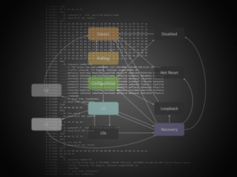
The state of the link is defined by a Link Training and Status State Machine (LTSSM). From an initial state, the state machine goes through various major states (Detect, Polling, Configuration) to train and configure the link before being fully in a link-up state (L0). The initialisation states also have sub-state which we will discuss shortly.
In addition, there are various powered-down states of varying degrees from L0s to L1 and L2, with L2 being all but powered off. The link can also be put into a loopback mode for test and debug, or a ‘hot reset’ state to send the link back to its initial state. The disabled state is for configured links where communications are suspended. Many of these ancillary states can be entered from the recovery state, but the main purpose of this state is to allow a configured link to change data rates, establishing lock and deskew for the new rate. Note that many of these states can be entered if directed from a higher layer, or if the link receives a particular TS ordered set where the control symbol has a particular bit set. For example, if a receiver receives two consecutive TS1 ordered sets with the Disable Link Bit asserted in the control symbol (see diagram above), the state will be forced to the Disabled state.
The diagram below shows these main states and the paths between them:

From power-up, then, the main flow is from the Detect state which checks what’s connected electrically and that it’s electrically idle. After this it enters the polling state where both ends start transmitting TS ordered sets and waits to receive a certain number of ordered sets from the other link. Polarity inversion is done in this state. After this, the Configuration state does a multitude of things with both ends sending ordered sets moving through assigning a link number (or numbers if splitting) and the lane numbers, with lane reversal if supported. In the configuration state the received TS ordered sets may direct the next state to be Disabled or Loopback and, in addition, scrambling may be disabled. Deskewing will be completed by the end of this state and the link will now be ’up’ and the state enters L0, the normal link-up state (assuming not directed to Loopback or Disabled).
As mentioned before, the initialisation states have sub-states, and the diagram below lists these states, what’s transmitted on those states and the condition to move to the next state.

In the Detect.Quiet state the link waits for Electrical Idle to be broken. Electrical Idle (or not) is done with analogue circuitry, though it may be inferred with the absence of received packets or TS OSs, depending on the current state. When broken, Detect.Active performs a Receiver Detect by measuring for a DC impedance (40 Ω – 60Ω for PCIe 2.0) on the line. Moving into Polling.Active both ends start transmitting TS1 ordered sets with the lane and link numbers set to the PAD symbol. The wait to have sent at least 1024 TSs and received 8 (or their inverse), before moving to Polling.Config. Here they start transmitting TS2 ordered sets with link and lane set to PAD, having inverted the RX lanes as necessary. The state then waits for transmitting at least 16 TS2s (after receiving one) and receives at least 8.
Now we move to Config.LinkWidth.Start. It is this, and the next state, that the viable link width or split is configured using different link numbers for each viable group of lanes. Here the upstream link (e.g., the endpoint) starts transmitting TS1s again with link and lane set to PAD. The downstream link (e.g., from root complex) start transmitting TS1s with a chosen link number and the lane number set to PAD. The upstream link responds to the receiving a minimum of two TS1s with a link number by sending back the TS1 with that link value and moves to Config.LinkWidth.Accept. The downstream will move to the same state when it has received to TS1s with a non-PAD link number. At this point the downstream link will transmit TS1s with assigned lane numbers whilst the upstream will initially continue to transmit TS1s with the lanes at PAD but will respond by matching the lane numbers on its TS1 transmissions (or possibly lane reversed) and then move to Config.Lanenum.Wait. The downstream link will move to this state on receiving TS1s with non-PAD lanes. This state is to allow for up to 1ms of time to settle errors or deskew that could give false link width configuration. The downstream will start transmitting TS2s when it has seen two consecutive TS1s, and the upstream lanes will respond when it has received two consecutive TS2s. At this point the state is Config.Complete and will move to Config.Idle after receiving eight consecutive TS2s whilst sending them. The lanes start sending IDL symbols and will move to state L0 (LinkUp=1) after receiving eight IDL symbols and have sent at least sixteen after seeing the first IDL.
The diagram below summarises these described steps for a normal non-split link initialisation.

To summarise these steps each link sends training sequences of a certain type and with certain values for link and lane values. When a certain number of TSs are seen, and on which lanes, the state is advanced, and configurations are set. There is a slight asymmetry in that a downstream link will switch type first to lead the upstream link into the next state. By the end of the process the link is configured for width, link number and lane assignment, with link reversal, lane inversion, and disabled scrambling where indicated. There are many variations of possible flow, such as being directed to Disabled or Loopback, or timeouts forcing the link back to Detect from Configuration states etc., which we want to describe in detail here.
A fragment of the output from the start of the link initialisation of the pcievhost model is shown below:

You can try this out for yourselves by retrieving the pcievhost repository, along with the virtual processor (VProc), and running the default test.
Compliance Pattern
The is an additional Polling state, Polling.Compliance, that is entered if, at Detect, if at least a single lane never exited Electrical Idle during Polling.Active. This implies that some passive test equipment is attached to measure transmitter electrical compliance. The transmitter must then output the compliance pattern, which is, for 8b/10b K28.5, D21.5, K28.5 and D10.2, repeated. For multiple lane devices, a two-symbol delay is introduced on every eighth lane, and then scrolled around in one lane steps at the end of the sequence.
Since this is a test mode, we will not detail this any further here, but it must be available in an implementation.
SERDES Interface and PIPE
The PCIe protocol runs serial lanes at high speed. As of version 6.0 this is 64GT/s (that is, raw bits). The SERDES that drives these serial lines at these high rates are complex and vary between manufactures and ASIC processes. The ‘Phy Interface for PCI Express’ (PIPE) was developed, by Intel, to standardize the interface between the logical protocol that we have been discussing, and the PHY sub-layer. It is not strictly part of the PCIe specification but is used so ubiquitously that I have included an overview here.
The PIPE specification conceptually splits the Physical layer into a media access layer (MAC) which includes the link training and status state machine (LTSSM), with the ordered sets and lane to lane deskew logic, a Physical Coding Sub-layer (PCS) with 8b/10b or 128b/130b codecs, RX detection and elastic buffering, and a Physical Media Attachment (PMA) with the analogue buffers and SERDES etc. The PIPE then standardizes the interface between the MAC and the PCS. The diagram below shows an overview of the PIPE signalling between the MAC and PCS:

The transmit data (TxData) carries the bytes for transmission. This could be wider than a byte, with 16- and 32-bit inputs allowed. The TxDataK signal indicates wither the byte is control symbol (K symbol in 8b/10b parlance). If the data interface is wider than a byte then this signal will have one wire per byte. The command signals are made up of various control signal inputs that we will discuss shortly. The data receive side mirrors the data transmit side with RxData and RxDataK signals. A set of Status signals are returned from the receiver, discussed shortly. The CLK input is implementation dependent on its specification but provides a reference for TX and RX bit-rate clock. The PCLK is the parallel data clock that all data transfers are referenced from.
The transmit command signals are summarised in the following table for PIPE version 2.00.

The receive status signals are summarised in the following table for PIPE version 2.00.

Hopefully from the tables it is easy to see how, via the PIPE interface signaling, MAC logic can control PHY state in a simple way and receive PHY status to indicate how it may transition through the LTSSM for initialisation and power down states.
The use of the PIPE standard makes development and verification much easier and allows Physical layer logic to be more easily migrated to different SERDES solutions. Usually, ASIC or IP vendors will provide IP that has this PIPE standard interface and will implement the PCS and PMA functions themselves. The vendor specific MAC logic, then, becomes more generic.
Conclusions
In this article we have looked at how PCIe is organized, with Root Complex, Switches and Endpoints, in a definite flow from upstream to downstream. We have seen that a PCIe link can be from 1 to 32 differential serial ‘lanes’. Bytes are scrambled (if data) and then encoded into DC free symbols (8b/10b or 128b/130b). Ordered Sets are defined for waking up a link from idle, link bit and symbol lock and lane-to-lane deskew. Training sequence Ordered sets are used to bring up a link from electrically idle to configured and initialized, configuring parameters as it does so or, optionally, forcing to non-standard states. Additional states are used for powered down modes of varying degrees, and a recovery state to update to higher link speed if supported. We also looked at the complementary PIPE specification for virtualizing away SERDES and PHY details to a standard interface.
We dwelt on the LTSSM at some length as this is the more complex aspect of the physical layer protocol, and the only remaining aspects of this layer are how the physical layer carries the higher data link layer and transaction layer packets. These, I think, are more suitably discussed alongside the descriptions of those layers, so this must wait for the next article.
Staff TLM Electrical Validation at Aurora
2movery impressive! Thanks so much for your time to putting this together. It save so much time for us to dig into original PCIe specification doc and get an idea how it works.
Freely Sharing Embedded Systems Programming Course (For details WhatsApp: +91 97908 73099))
3moThanks for sharing the critical information. Very useful.
Embedded software | Microprocessors | C++ Engineer
4moThat was really helpful , thanks for sharing .
Senior Hardware Design Engineer at Samsung semiconductor US
7mopdf version has been deleted could you update, please?
Graphics Hardware Engineer at Intel Corporation
1yThanks for making this valuable summary on PCIe!