HPC
NVIDIA Debuts Ampere Architecture with NVIDIA A100 & DGX A100 – A Game Changer for AI & HPC Workloads
9 min read

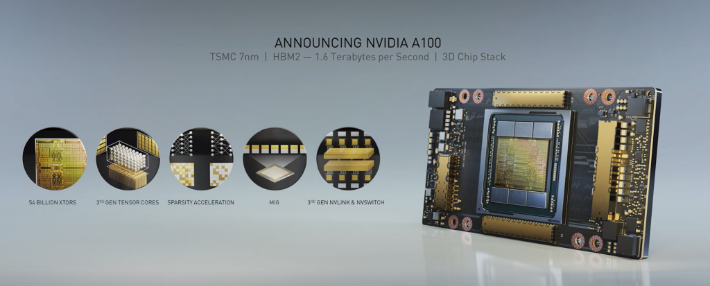
Due to the COVID-19 outbreak, GTC 2020 was shifted to an all virtual conference, and the long anticipated next generation NVIDIA GPU architecture announcement was subsequently delayed. However today, NVIDIA CEO Jensen Huang’s keynote took the virtual stage to announce NVIDIA’s all new GPU architecture, Ampere, and the first products that will be using it. At the center of this is a new GPU, the NVIDIA A100, and a new system, the NVIDIA DGX™ A100.
The NVIDIA A100 GPU is a technical design breakthrough fueled by five key innovations:
The NVIDIA A100 Tensor Core GPU delivers the next giant leap in NVIDIA’s accelerated data center platform, providing unmatched acceleration at every scale and enabling these innovators to do their life’s work within their lifetime. A100 powers numerous application areas including HPC, genomics, 5G, rendering, deep learning, data analytics, data science, and robotics.
NVIDIA today set out a vision for the next generation of computing that shifts the focus of the global information economy from servers to a new class of powerful, flexible data centers.

| Product Architecture | Pascal P100 | Volta V100 | NVIDIA A100 |
|---|---|---|---|
| GPU Codename | GP100 | GV100 | GA100 |
| GPU Architecture | NVIDIA Pascal | NVIDIA Volta | NVIDIA Ampere |
| GPU Board Form Factor | SXM2 | SXM2 | SXM4 |
| SMs | 56 | 80 | 108 |
| TPCs | 28 | 40 | 54 |
| FP32 Cores / SM | 64 | 64 | 64 |
| FP32 Cores / GPU | 3584 | 5120 | 6912 |
| FP64 Cores / SM | 32 | 32 | 32 |
| FP64 Cores / GPU | 1792 | 2560 | 3456 |
| INT32 Cores / SM | NA | 64 | 64 |
| INT32 Cores / GPU | NA | 5120 | 6912 |
| Tensor Cores / SM | NA | 8 | 42 |
| Tensor Cores / GPU | NA | 640 | 432 |
| GPU Boost Clock | 1480 MHz | 1530 MHz | 1410 MHz |
| Peak FP16 Tensor TFLOPS with FP16 Accumulate1 | NA | 125 | 312/6243 |
| Peak FP16 Tensor TFLOPS with FP32 Accumulate1 | NA | 125 | 312/6243 |
| Peak BF16 Tensor TFLOPS with FP32 Accumulate1 | NA | NA | 312/6243 |
| Peak TF32 Tensor TFLOPS1 | NA | NA | 156/3123 |
| Peak FP64 Tensor TFLOPS1 | NA | NA | 19.5 |
| Peak INT8 Tensor TOPS1 | NA | NA | 624/12483 |
| Peak INT4 Tensor TOPS1 | NA | NA | 1248/24963 |
| Peak FP16 TFLOPS1 | 21.2 | 31.4 | 78 |
| Peak BF16 TFLOPS1 | NA | NA | 39 |
| Peak FP32 TFLOPS1 | 10.6 | 15.7 | 19.5 |
| Peak FP64 TFLOPS1 | 5.3 | 7.8 | 9.7 |
| Peak INT32 TOPS1 | NA | 15.7 | 19.5 |
| Texture Units | 224 | 320 | 432 |
| Memory Interface | 4096-bit HBM2 | 4096-bit HBM2 | 5120-bit HBM2 |
| Memory Size | 16 GB | 32 GB / 16 GB | 40 GB |
| Memory Data Rate | 703 MHz DDR | 877.5 MHz DDR | 1215 MHz DDR |
| Memory Bandwidth | 720 GB/sec | 900 GB/sec | 1.6 TB/sec |
| L2 Cache Size | 4096 KB | 6144 KB | 40960 KB |
| Shared Memory Size / SM | 64 KB | Configurable up to 96 KB | Configurable up to 164 KB |
| Register File Size / SM | 256 KB | 256 KB | 256 KB |
| Register File Size / GPU | 14336 KB | 20480 KB | 27648 KB |
| TDP | 300 Watts | 300 Watts | 400 Watts |
| Transistors | 15.3 billion | 21.1 billion | 54.2 billion |
| GPU Die Size | 610 mm² | 815 mm² | 826 mm2 |
| TSMC Manufacturing Process | 16 nm FinFET+ | 12 nm FFN | 7 nm N7 |
1) Peak rates are based on the GPU boost clock.
2) Four Tensor Cores in an A100 SM have 2x the raw FMA computational power of eight Tensor Cores in a GV100 SM.
3) Effective TOPS / TFLOPS using the new Sparsity feature.
source: https://devblogs.nvidia.com/nv...

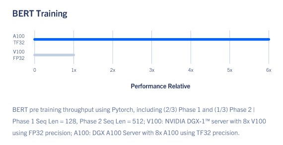
AI models are exploding in complexity as they take on next-level challenges such as accurate conversational AI and deep recommender systems. Training them requires massive compute power and scalability.
NVIDIA A100’s third-generation Tensor Cores with Tensor Float (TF32) precision provide up to 20x higher performance over the prior generation with zero code changes and an additional 2x boost with automatic mixed precision and FP16. When combined with third-generation NVIDIA® NVLink®, NVIDIA NVSwitch™, PCI Gen4, NVIDIA Mellanox InfiniBand, and the NVIDIA Magnum IO™ software SDK, it’s possible to scale to thousands of A100 GPUs. This means that large AI models like BERT can be trained in just 37 minutes on a cluster of 1,024 A100s, offering unprecedented performance and scalability.
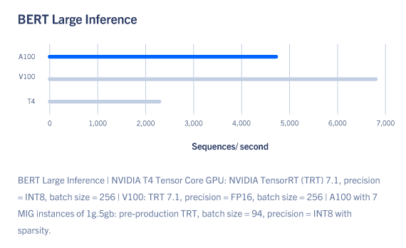
A100 introduces groundbreaking new features to optimize inference workloads. It brings unprecedented versatility by accelerating a full range of precisions, from FP32 to FP16 to INT8 and all the way down to INT4. Multi-Instance GPU (MIG) technology allows multiple networks to operate simultaneously on a single A100 GPU for optimal utilization of compute resources. And structural sparsity support delivers up to 2x more performance on top of A100’s other inference performance gains.
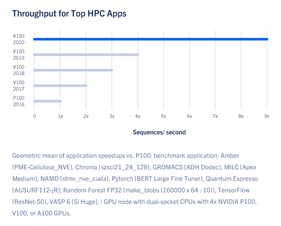
To unlock next-generation discoveries, scientists look to simulations to better understand complex molecules for drug discovery, physics for potential new sources of energy, and atmospheric data to better predict and prepare for extreme weather patterns.
A100 introduces double-precision Tensor Cores, providing the biggest milestone since the introduction of double-precision computing in GPUs for HPC. This enables researchers to reduce a 10-hour, double-precision simulation running on NVIDIA V100 Tensor Core GPUs to just four hours on A100. HPC applications can also leverage TF32 precision in A100’s Tensor Cores to achieve up to 10x higher throughput for single-precision dense matrix multiply operations.

Due to the COVID-19 outbreak, GTC 2020 was shifted to an all virtual conference, and the long anticipated next generation NVIDIA GPU architecture announcement was subsequently delayed. However today, NVIDIA CEO Jensen Huang’s keynote took the virtual stage to announce NVIDIA’s all new GPU architecture, Ampere, and the first products that will be using it. At the center of this is a new GPU, the NVIDIA A100, and a new system, the NVIDIA DGX™ A100.
The NVIDIA A100 GPU is a technical design breakthrough fueled by five key innovations:
The NVIDIA A100 Tensor Core GPU delivers the next giant leap in NVIDIA’s accelerated data center platform, providing unmatched acceleration at every scale and enabling these innovators to do their life’s work within their lifetime. A100 powers numerous application areas including HPC, genomics, 5G, rendering, deep learning, data analytics, data science, and robotics.
NVIDIA today set out a vision for the next generation of computing that shifts the focus of the global information economy from servers to a new class of powerful, flexible data centers.
| Product Architecture | Pascal P100 | Volta V100 | NVIDIA A100 |
|---|---|---|---|
| GPU Codename | GP100 | GV100 | GA100 |
| GPU Architecture | NVIDIA Pascal | NVIDIA Volta | NVIDIA Ampere |
| GPU Board Form Factor | SXM2 | SXM2 | SXM4 |
| SMs | 56 | 80 | 108 |
| TPCs | 28 | 40 | 54 |
| FP32 Cores / SM | 64 | 64 | 64 |
| FP32 Cores / GPU | 3584 | 5120 | 6912 |
| FP64 Cores / SM | 32 | 32 | 32 |
| FP64 Cores / GPU | 1792 | 2560 | 3456 |
| INT32 Cores / SM | NA | 64 | 64 |
| INT32 Cores / GPU | NA | 5120 | 6912 |
| Tensor Cores / SM | NA | 8 | 42 |
| Tensor Cores / GPU | NA | 640 | 432 |
| GPU Boost Clock | 1480 MHz | 1530 MHz | 1410 MHz |
| Peak FP16 Tensor TFLOPS with FP16 Accumulate1 | NA | 125 | 312/6243 |
| Peak FP16 Tensor TFLOPS with FP32 Accumulate1 | NA | 125 | 312/6243 |
| Peak BF16 Tensor TFLOPS with FP32 Accumulate1 | NA | NA | 312/6243 |
| Peak TF32 Tensor TFLOPS1 | NA | NA | 156/3123 |
| Peak FP64 Tensor TFLOPS1 | NA | NA | 19.5 |
| Peak INT8 Tensor TOPS1 | NA | NA | 624/12483 |
| Peak INT4 Tensor TOPS1 | NA | NA | 1248/24963 |
| Peak FP16 TFLOPS1 | 21.2 | 31.4 | 78 |
| Peak BF16 TFLOPS1 | NA | NA | 39 |
| Peak FP32 TFLOPS1 | 10.6 | 15.7 | 19.5 |
| Peak FP64 TFLOPS1 | 5.3 | 7.8 | 9.7 |
| Peak INT32 TOPS1 | NA | 15.7 | 19.5 |
| Texture Units | 224 | 320 | 432 |
| Memory Interface | 4096-bit HBM2 | 4096-bit HBM2 | 5120-bit HBM2 |
| Memory Size | 16 GB | 32 GB / 16 GB | 40 GB |
| Memory Data Rate | 703 MHz DDR | 877.5 MHz DDR | 1215 MHz DDR |
| Memory Bandwidth | 720 GB/sec | 900 GB/sec | 1.6 TB/sec |
| L2 Cache Size | 4096 KB | 6144 KB | 40960 KB |
| Shared Memory Size / SM | 64 KB | Configurable up to 96 KB | Configurable up to 164 KB |
| Register File Size / SM | 256 KB | 256 KB | 256 KB |
| Register File Size / GPU | 14336 KB | 20480 KB | 27648 KB |
| TDP | 300 Watts | 300 Watts | 400 Watts |
| Transistors | 15.3 billion | 21.1 billion | 54.2 billion |
| GPU Die Size | 610 mm² | 815 mm² | 826 mm2 |
| TSMC Manufacturing Process | 16 nm FinFET+ | 12 nm FFN | 7 nm N7 |
1) Peak rates are based on the GPU boost clock.
2) Four Tensor Cores in an A100 SM have 2x the raw FMA computational power of eight Tensor Cores in a GV100 SM.
3) Effective TOPS / TFLOPS using the new Sparsity feature.
source: https://devblogs.nvidia.com/nv...
AI models are exploding in complexity as they take on next-level challenges such as accurate conversational AI and deep recommender systems. Training them requires massive compute power and scalability.
NVIDIA A100’s third-generation Tensor Cores with Tensor Float (TF32) precision provide up to 20x higher performance over the prior generation with zero code changes and an additional 2x boost with automatic mixed precision and FP16. When combined with third-generation NVIDIA® NVLink®, NVIDIA NVSwitch™, PCI Gen4, NVIDIA Mellanox InfiniBand, and the NVIDIA Magnum IO™ software SDK, it’s possible to scale to thousands of A100 GPUs. This means that large AI models like BERT can be trained in just 37 minutes on a cluster of 1,024 A100s, offering unprecedented performance and scalability.
A100 introduces groundbreaking new features to optimize inference workloads. It brings unprecedented versatility by accelerating a full range of precisions, from FP32 to FP16 to INT8 and all the way down to INT4. Multi-Instance GPU (MIG) technology allows multiple networks to operate simultaneously on a single A100 GPU for optimal utilization of compute resources. And structural sparsity support delivers up to 2x more performance on top of A100’s other inference performance gains.
To unlock next-generation discoveries, scientists look to simulations to better understand complex molecules for drug discovery, physics for potential new sources of energy, and atmospheric data to better predict and prepare for extreme weather patterns.
A100 introduces double-precision Tensor Cores, providing the biggest milestone since the introduction of double-precision computing in GPUs for HPC. This enables researchers to reduce a 10-hour, double-precision simulation running on NVIDIA V100 Tensor Core GPUs to just four hours on A100. HPC applications can also leverage TF32 precision in A100’s Tensor Cores to achieve up to 10x higher throughput for single-precision dense matrix multiply operations.